EP3259796B1 - Battery cell for a battery of a motor vehicle, battery, and motor vehicle - Google Patents
Battery cell for a battery of a motor vehicle, battery, and motor vehicle Download PDFInfo
- Publication number
- EP3259796B1 EP3259796B1 EP16704025.2A EP16704025A EP3259796B1 EP 3259796 B1 EP3259796 B1 EP 3259796B1 EP 16704025 A EP16704025 A EP 16704025A EP 3259796 B1 EP3259796 B1 EP 3259796B1
- Authority
- EP
- European Patent Office
- Prior art keywords
- battery cell
- battery
- housing
- carrier
- microelectronic
- Prior art date
- Legal status (The legal status is an assumption and is not a legal conclusion. Google has not performed a legal analysis and makes no representation as to the accuracy of the status listed.)
- Active
Links
Images


Classifications
-
- H—ELECTRICITY
- H01—ELECTRIC ELEMENTS
- H01M—PROCESSES OR MEANS, e.g. BATTERIES, FOR THE DIRECT CONVERSION OF CHEMICAL ENERGY INTO ELECTRICAL ENERGY
- H01M10/00—Secondary cells; Manufacture thereof
- H01M10/42—Methods or arrangements for servicing or maintenance of secondary cells or secondary half-cells
- H01M10/425—Structural combination with electronic components, e.g. electronic circuits integrated to the outside of the casing
- H01M10/4257—Smart batteries, e.g. electronic circuits inside the housing of the cells or batteries
-
- G—PHYSICS
- G01—MEASURING; TESTING
- G01R—MEASURING ELECTRIC VARIABLES; MEASURING MAGNETIC VARIABLES
- G01R31/00—Arrangements for testing electric properties; Arrangements for locating electric faults; Arrangements for electrical testing characterised by what is being tested not provided for elsewhere
- G01R31/36—Arrangements for testing, measuring or monitoring the electrical condition of accumulators or electric batteries, e.g. capacity or state of charge [SoC]
- G01R31/3644—Constructional arrangements
- G01R31/3648—Constructional arrangements comprising digital calculation means, e.g. for performing an algorithm
-
- G—PHYSICS
- G01—MEASURING; TESTING
- G01R—MEASURING ELECTRIC VARIABLES; MEASURING MAGNETIC VARIABLES
- G01R31/00—Arrangements for testing electric properties; Arrangements for locating electric faults; Arrangements for electrical testing characterised by what is being tested not provided for elsewhere
- G01R31/36—Arrangements for testing, measuring or monitoring the electrical condition of accumulators or electric batteries, e.g. capacity or state of charge [SoC]
- G01R31/396—Acquisition or processing of data for testing or for monitoring individual cells or groups of cells within a battery
-
- G—PHYSICS
- G01—MEASURING; TESTING
- G01R—MEASURING ELECTRIC VARIABLES; MEASURING MAGNETIC VARIABLES
- G01R31/00—Arrangements for testing electric properties; Arrangements for locating electric faults; Arrangements for electrical testing characterised by what is being tested not provided for elsewhere
- G01R31/44—Testing lamps
-
- H—ELECTRICITY
- H01—ELECTRIC ELEMENTS
- H01M—PROCESSES OR MEANS, e.g. BATTERIES, FOR THE DIRECT CONVERSION OF CHEMICAL ENERGY INTO ELECTRICAL ENERGY
- H01M10/00—Secondary cells; Manufacture thereof
- H01M10/42—Methods or arrangements for servicing or maintenance of secondary cells or secondary half-cells
- H01M10/48—Accumulators combined with arrangements for measuring, testing or indicating the condition of cells, e.g. the level or density of the electrolyte
-
- H—ELECTRICITY
- H01—ELECTRIC ELEMENTS
- H01M—PROCESSES OR MEANS, e.g. BATTERIES, FOR THE DIRECT CONVERSION OF CHEMICAL ENERGY INTO ELECTRICAL ENERGY
- H01M10/00—Secondary cells; Manufacture thereof
- H01M10/42—Methods or arrangements for servicing or maintenance of secondary cells or secondary half-cells
- H01M10/425—Structural combination with electronic components, e.g. electronic circuits integrated to the outside of the casing
- H01M2010/4271—Battery management systems including electronic circuits, e.g. control of current or voltage to keep battery in healthy state, cell balancing
-
- H—ELECTRICITY
- H01—ELECTRIC ELEMENTS
- H01M—PROCESSES OR MEANS, e.g. BATTERIES, FOR THE DIRECT CONVERSION OF CHEMICAL ENERGY INTO ELECTRICAL ENERGY
- H01M2200/00—Safety devices for primary or secondary batteries
-
- H—ELECTRICITY
- H01—ELECTRIC ELEMENTS
- H01M—PROCESSES OR MEANS, e.g. BATTERIES, FOR THE DIRECT CONVERSION OF CHEMICAL ENERGY INTO ELECTRICAL ENERGY
- H01M2220/00—Batteries for particular applications
- H01M2220/20—Batteries in motive systems, e.g. vehicle, ship, plane
-
- Y—GENERAL TAGGING OF NEW TECHNOLOGICAL DEVELOPMENTS; GENERAL TAGGING OF CROSS-SECTIONAL TECHNOLOGIES SPANNING OVER SEVERAL SECTIONS OF THE IPC; TECHNICAL SUBJECTS COVERED BY FORMER USPC CROSS-REFERENCE ART COLLECTIONS [XRACs] AND DIGESTS
- Y02—TECHNOLOGIES OR APPLICATIONS FOR MITIGATION OR ADAPTATION AGAINST CLIMATE CHANGE
- Y02E—REDUCTION OF GREENHOUSE GAS [GHG] EMISSIONS, RELATED TO ENERGY GENERATION, TRANSMISSION OR DISTRIBUTION
- Y02E60/00—Enabling technologies; Technologies with a potential or indirect contribution to GHG emissions mitigation
- Y02E60/10—Energy storage using batteries
Definitions
- the invention relates to a battery cell for a battery of a motor vehicle with a galvanic element, a battery cell housing for receiving the galvanic element and at least two microelectronic circuits for monitoring the battery cell.
- the invention also relates to a battery and a motor vehicle.
- a galvanic element is usually arranged in each case in a battery cell housing.
- several battery cells can be interconnected to form a battery.
- These batteries are used nowadays in particular as traction batteries in motor vehicles, for example in electric or hybrid vehicles, for driving the motor vehicles.
- the batteries When the batteries are used in motor vehicles, however, they must meet certain requirements.
- the traction batteries can provide a few hundred volts, special safety measures must be taken, for example to avoid endangering people.
- a high availability of the battery must be guaranteed. This availability is particularly dependent on the degree of damage or aging of the battery. Since the battery cells have fluctuations in their capacity and internal resistance due to production, they are usually charged and discharged at different speeds. This can damage the battery if, for example, individual cells are deeply discharged or overcharged.
- the WO 2013/143755 A1 discloses a sensor device for a battery cell of an electrical energy store.
- the battery cell has a housing, the sensor device having a detection device for detecting sensor data, which can be arranged within the housing. Furthermore, the sensor device has an evaluation device for evaluating the sensor data, which can be arranged inside and outside the housing.
- the US 2014/0184165 A1 discloses a secondary battery comprising a sensor that is a measurement unit, a microcontroller unit that is a determination unit, and a memory that is a storage unit.
- the sensor measures the conditions of the secondary battery, such as the remaining battery power, the voltage, the current and the temperature.
- the microcontroller unit carries out arithmetic processing of the measurement results and determines the operating status of the secondary battery.
- the microcontroller unit stores the measurement result in the memory according to the operating status of the secondary battery.
- integration of the batteries and their electronics in the motor vehicle is a major challenge.
- the object of the present invention is to integrate microelectronic circuits for monitoring a battery cell in the most space-saving way possible in order to minimize the space required by the battery cell.
- the battery cell according to the invention for a battery of a motor vehicle comprises a galvanic element, a battery cell housing for receiving of the galvanic element and at least two microelectronic circuits for monitoring the battery cell.
- a first of the at least two microelectronic circuits is applied to a first carrier and a second of the at least two microelectronic circuits is applied to a separate second carrier.
- the two carriers are arranged one above the other and thus form a stack, so that an upper side of the first carrier faces a lower side of the second carrier.
- the stack comprising the two carriers is mechanically and / or thermally coupled to an inside of a wall of the battery cell housing.
- a cuboid battery cell housing for example, and a galvanic cell, for example, arranged therein
- cavities between the galvanic cell and the battery cell housing. These cavities can be used sensibly for receiving the stack.
- the stack is attached to the inner wall of the battery cell housing.
- waste heat which is usually produced by the microelectronic circuits during operation, can be dissipated to the battery cell housing and finally to the environment outside the battery cell housing.
- the stack can be cooled in an advantageous manner.
- the galvanic element is designed in particular as a secondary cell which can be discharged to supply an electrical component and recharged again after the discharge.
- the galvanic element comprises two electrodes and an electrolyte in a manner known per se.
- the galvanic element is arranged in the battery cell housing, which is made of aluminum, for example.
- the galvanic element can be electrically isolated from the battery cell housing.
- an insulating material can be arranged between an inside of a wall of the battery cell housing and the galvanic element.
- the battery cell housing has two particularly exposed battery poles or battery connections, one battery pole each being electrically connected to an electrode of the galvanic element .
- the battery cell has the at least two microelectronic circuits.
- the battery cell provided with microelectronic circuits can also be referred to as an intelligent battery cell.
- Each of the microelectronic circuits can include at least one so-called one-chip system or SoC (system-on-a-chip).
- SoC system-on-a-chip
- various functions of a system for example in the form of an integrated circuit (IC-Integrated Circuit), are integrated or combined or programmed on a common chip or semiconductor substrate.
- the system or the integrated circuit can comprise various elements or components, for example semiconductor components, logic circuits, clock generators, active and passive components, sensors or FPGAs (Field Programmable Gate Arrays), which when connected together provide a specific functionality.
- Several integrated circuits or one-chip systems can be electrically connected to one another via conductor tracks of the microelectronic circuit.
- each of the microelectronic circuits is now arranged on a separate carrier.
- the carriers can for example be designed as printed circuit boards.
- the circuit boards can be equipped with the chips and the conductor tracks of the respective microelectronic circuit on one side as well as on both sides.
- the circuit boards can be designed as flexible circuit boards, so-called PCB foils (PCB printed circuit board).
- PCB foils have a particularly low weight and a particularly small thickness, while at the same time having high mechanical flexural strength and high temperature resistance.
- the circuit boards are designed as so-called injection-molded circuit carriers or MID (Molded Interconnect Devices.
- MID Molded Interconnect Devices.
- Such carriers are usually injection-molded plastic components, also to which metallic conductor tracks are applied using special processes.
- the plastic components can be three-dimensional or plastic components A carrier designed as an MID is therefore particularly flexible.
- These separate carriers are stacked one on top of the other to form a layered structure.
- the first carrier is arranged under the second carrier so that the top of the first carrier is the bottom of the facing the second carrier.
- the upper side of the first carrier and the lower side of the second carrier overlap at least in some areas.
- the carriers and with them the microelectronic circuits can be arranged in the battery cell in a particularly space-saving manner.
- electrical contact can be made with the chips on both circuit boards via particularly short conduction paths.
- the microelectronic circuits can advantageously be supplied with electrical energy by the galvanic element itself. This creates a self-sufficient system.
- the first microelectronic circuit is arranged in a first housing and the second microelectronic circuit is arranged in a second housing.
- the two housed or encased microelectronic circuits are applied to the respective carrier, the two carriers being electrically and / or mechanically coupled to one another.
- a carrier with an electronic circuit which is arranged in a housing is also referred to as a package.
- the stack created by arranging two or more packages on top of one another is also referred to as package-on-package (PoP).
- the packages that is to say the carriers with the microelectronic circuits housed on them, can be manufactured separately and independently of one another. For example, the production of the packages can be transferred to different manufacturers with their respective expertise. The individual packages can then be put together in a particularly flexible and requirement-specific manner to form the stack, i.e. the package-on-package. In other words, this means that a functionality of the stack can be defined and provided in a flexible manner by combining the corresponding packages.
- the packages, in particular the carriers can be soldered together for electrical and mechanical connection. In the event of a defect in a package or a chip in the microelectronic circuit of the package, the corresponding package can also be exchanged in a particularly simple manner. Thanks to the modular manufacture of the package, the packages can also be tested individually and, if necessary, replaced in the event of a defect.
- the first carrier and the second carrier are arranged together in a housing.
- the two carriers are mechanically and / or electrically coupled to one another within the common housing.
- the arrangement of the carriers in a common housing is also referred to as a system-in-package (SiP).
- SiP system-in-package
- electrical contact surfaces can be provided in a bottom surface of the common housing, for example, which are electrically connected to the individual carriers via bonding wires, for example.
- the housing or housings are made from a material that is insensitive to an electrolyte of the galvanic element, in particular a ceramic.
- the housings When the stack is arranged within the battery cell, the housings must not be dissolved or corroded by the liquid, electrolyte or other chemical substances, for example. For example, corrosion can change the chemical composition of the electrolyte and consequently the behavior of the battery cell, in particular of the galvanic element. If the housing is destroyed, the chemical substances can come into contact with the microelectronic circuits and thus destroy them.
- the housings are preferably made of ceramics and / or special plastics or similar corrosion-resistant materials. Thus, protection of the microelectronic circuits can be reliably provided.
- At least one sensor element and / or at least one memory element and / or at least one communication device and / or at least one microprocessor are particularly preferably provided as the elements of the microelectronic circuit.
- the at least one sensor element is used to detect a physical and / or chemical property of the battery cell.
- a physical and / or chemical property can, for example, be a temperature within the battery cell housing, a pressure within the battery cell housing, or an acceleration of the battery cell or a chemical composition of the electrolyte of the galvanic element.
- the data recorded by the at least one sensor element can be stored on the at least one memory element.
- a state of the battery cell can thus be monitored over an entire operating period or service life of the battery cell.
- the at least one microprocessor can be designed, for example, to evaluate the data recorded by the sensor element and / or the data stored in the memory element, for example to detect a change in a physical and / or chemical property over an operating time of the battery cell.
- the at least one communication device can be designed, for example, to communicate with components inside and outside the battery cell.
- a component outside the battery cell can be, for example, a battery management system of the motor vehicle or another battery cell.
- a component within the cell can, for example, be an element on the respective other carrier or also a sensor which is arranged within the battery cell housing at a location different from the location of the stack.
- the communication device can be designed, for example, as a wireless transmission device which, for example, sends and / or receives data via Bluetooth or WLAN, but also, for example, via ultrasound and light waves.
- the invention also includes a battery having a series connection and / or parallel connection of at least two battery cells according to the invention.
- a motor vehicle according to the invention comprises at least one battery according to the invention.
- the motor vehicle can be configured, for example, as a passenger vehicle, in particular as an electric or hybrid vehicle.
- the motor vehicle can, however, also be designed as an electrically operated motorcycle or bicycle.
- the battery in a stationary energy storage system. It can be provided, for example, that the battery, which was provided in a motor vehicle, continues to be used as a so-called second life battery in the stationary energy storage system.
- Fig. 1 shows a battery cell 1 with a galvanic element 2 and a battery cell housing 3.
- the galvanic element 2 is arranged in the battery cell housing 3.
- the battery cell housing 3 can be made of aluminum, for example.
- the battery cell housing 3 here has two exposed or raised connections 4 and 5, via which electrical energy, for example to supply an electrical component, can be tapped and via which the battery cell 1 can be supplied with electrical energy for charging the battery cell 1 or via which the battery cell 1 can be interconnected with other similar battery cells to form a battery.
- a battery can be arranged, for example, in a motor vehicle (not shown here) for driving the motor vehicle.
- Such a battery can, however, also be provided in a stationary energy supply system (not shown here).
- the battery cell 1 has a first microelectronic circuit 6 and a second microelectronic circuit 7.
- the microelectronic circuits 6 and 7 serve to monitor the battery cell 1.
- the battery cell 1 provided with the microelectronic circuits 6 and 7 is referred to as an intelligent battery cell 1.
- Each of the microelectronic circuits 6 and 7 can include at least one so-called one-chip system or system-on-a-chip SoC, which is shown in FIG Fig. 2 is shown.
- the one-chip system SoC various elements 8 are arranged on a chip 9 or a semiconductor substrate and, when connected together, provide a specific functionality.
- the elements 8 can for example be semiconductor components, Be sensors, memory elements, logic circuits, microprocessors or communication devices.
- several such one-chip systems SoC can be connected to one another to form a microelectronic circuit, for example via electrical conductor tracks.
- the first microelectronic circuit 6 is arranged on a first carrier 10 and the second microelectronic circuit is arranged on a second carrier 11.
- the carriers 10 and 11 equipped with the microelectronic circuits 6 and 7 are arranged one above the other and form a stack 12 in which an upper side 13 of the first carrier 10 faces an underside 14 of the second carrier 11.
- the stack 12 is arranged inside the battery cell housing 3 in a cavity 16 which is formed between an inner side 15 of a wall of the battery cell housing 3 and the galvanic element 2.
- the stack 12 is thermally coupled to the inside 15 of the battery cell housing 3. Waste heat which is produced by the microelectronic circuits 6 and 7 during operation can thus be dissipated to the battery cell housing 3 and finally to the surroundings of the battery cell 1.
- energy can also be transferred via such a wireless connection 19.
- a transformer not shown here, can be provided, for example, through which energy is transmitted in the form of magnetic waves.
- the components 18 and / or the elements 8 of the microelectronic circuits 6 and 7 can also be designed as so-called low-power components or as so-called ultra-low-power components thus have a low energy consumption.
- the components 18 and / or the elements 8 of the microelectronic circuits 6 and 7 can be designed as so-called nanogenerators and thus obtain energy from the environment, for example from a temperature gradient within the battery cell housing 3.
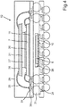
- Fig. 3 shows a schematic representation of the stack 12.
- the first carrier 10, the second carrier 11, a third carrier 20, a fourth carrier 21 and a fifth carrier 22 are stacked on top of one another.
- the carriers 10, 11, 20, 21, 22 each have a microelectronic circuit and are arranged in a common housing 23, which is shown here open in certain areas.
- the common housing 23 has several electrical contact surfaces 24 which are electrically connected to the carriers 10, 11, 20, 21, 22, in particular their microelectronic circuits, via bond connections 25.
- the stack 12, in which the carriers 10, 11, 20, 21, 22 with their microelectronic circuits are arranged in the common housing 23, is also referred to as a system-in-package (SiP).
- SiP system-in-package
- Fig. 4 shows a further stack 12 in a sectional view.
- the first microelectronic circuit 6 is arranged in a first housing 26.
- the first housing 26 is arranged on the first carrier 10.
- the first housing 26 with the first microelectronic circuit 6 and the first carrier 10 form a so-called first package.
- the second carrier 11 with the second microelectronic circuit 7, the third carrier 20 with a third microelectronic circuit 27 and the fourth carrier 21 with a fourth microelectronic circuit 28 are arranged in a second housing 29 and thus form a second package.
- the microelectronic circuits 7, 27, 28 are electrically connected to electrical contact surfaces 24 of a housing bottom 30 of the second housing 29 via soldered connections.
- the second package here is designed as a system-in-package (SiP), as exemplified in FIG Fig. 3 is shown.
- the first and second packages are mechanically and electrically coupled to one another in that the electrical contact surfaces 24 of the housing bottom 30 are connected to electrical contact surfaces 24 of the first carrier 10 via an electrically conductive connection element 31, for example a soldered connection.
- the packages that are stacked on top of one another and contacted with one another form a so-called package-on-package.
- the first, lower package is referred to as the bottom package.
- the bottom package can for example comprise a logic circuit as the first microelectronic circuit 6.
- the second package seated on top of the bottom package is referred to as the top package.
- the top package can include, for example, a memory element or a memory module.
- the package-on-package can also include more than two packages.
- the stacking of the packages has the advantage that the individual microelectronic circuits 6, 7, 27, 28 can be tested separately. If, for example, a chip SoC of one of the microelectronic circuits 6, 7, 27, 28 is defective, this defective chip SoC or the package with the defective chip SoC can be replaced in a simple manner. Furthermore, a specific chip combination or a specific package combination can be specified until shortly before the individual packages are contacted, that is, until shortly before the soldering process. In the case of package-on-package, for example, the memory chip on top, that is to say the upper package which comprises the memory module, can be varied in memory size before the soldering process. Another advantage of the stack 12 according to FIG Fig. 4 consists in the short contact paths between the two packages. In this way, for example, the memory and the connection between two chips can be operated with high clock frequencies.
- the housings 23, 26, 29 are preferably made of a corrosion-resistant material that is not damaged or destroyed by the electrolyte of the galvanic element 2.
Description
Die Erfindung betrifft eine Batteriezelle für eine Batterie eines Kraftfahrzeugs mit einem galvanischen Element, einem Batteriezellengehäuse zum Aufnehmen des galvanischen Elementes und zumindest zwei mikroelektronischen Schaltungen zum Überwachen der Batteriezelle. Die Erfindung betrifft außerdem eine Batterie sowie ein Kraftfahrzeug.The invention relates to a battery cell for a battery of a motor vehicle with a galvanic element, a battery cell housing for receiving the galvanic element and at least two microelectronic circuits for monitoring the battery cell. The invention also relates to a battery and a motor vehicle.
Bei an sich bekannten Batteriezellen ist üblicherweise jeweils ein galvanisches Element in einem Batteriezellengehäuse angeordnet. Zum Bereitstellen einer bestimmten Spannung beziehungsweise eines bestimmen Stromes können mehrere Batteriezellen zu einer Batterie zusammengeschaltet werden. Diese Batterien werden heutzutage insbesondere als Traktionsbatterien in Kraftfahrzeugen, beispielsweise in Elektro- oder Hybridfahrzeugen, zum Antreiben der Kraftfahrzeuge eingesetzt. Beim Einsatz der Batterien in Kraftfahrzeugen müssen diese jedoch gewisse Anforderungen erfüllen. Da die Traktionsbatterien einige hundert Volt bereitstellen können, müssen besondere Sicherheitsmaßnahmen getroffen werden, um beispielsweise eine Gefährdung von Personen zu vermeiden. Außerdem muss eine hohe Verfügbarkeit der Batterie gewährleistet werden. Diese Verfügbarkeit ist insbesondere abhängig von einem Schädigungsgrad beziehungsweise einer Alterung der Batterie. Da die Batteriezellen fertigungsbedingt Schwankungen in ihrer Kapazität sowie in ihrem Innenwiderstand aufweisen, werden sie in der Regel unterschiedlich schnell geladen und entladen. Dabei kann es zu einer Schädigung der Batterie kommen, wenn einzelne Zellen beispielsweise tiefenentladen oder überladen werden.In the case of battery cells known per se, a galvanic element is usually arranged in each case in a battery cell housing. To provide a specific voltage or a specific current, several battery cells can be interconnected to form a battery. These batteries are used nowadays in particular as traction batteries in motor vehicles, for example in electric or hybrid vehicles, for driving the motor vehicles. When the batteries are used in motor vehicles, however, they must meet certain requirements. Since the traction batteries can provide a few hundred volts, special safety measures must be taken, for example to avoid endangering people. In addition, a high availability of the battery must be guaranteed. This availability is particularly dependent on the degree of damage or aging of the battery. Since the battery cells have fluctuations in their capacity and internal resistance due to production, they are usually charged and discharged at different speeds. This can damage the battery if, for example, individual cells are deeply discharged or overcharged.
Um eine Batterie oder einzelne Batteriezellen zu überwachen, sind aus dem Stand der Technik Maßnahmen bekannt. So zeigt die
Die
Die
Da in Kraftfahrzeugen jedoch nur ein begrenzter Bauraum verfügbar ist, ist eine Integration der Batterien sowie deren Elektronik in dem Kraftfahrzeug eine große Herausforderung.The
However, since only a limited installation space is available in motor vehicles, integration of the batteries and their electronics in the motor vehicle is a major challenge.
Es ist Aufgabe der vorliegenden Erfindung, mikroelektronische Schaltungen zur Überwachung einer Batteriezelle möglichst platzsparend zu integrieren, um einen Platzbedarf der Batteriezelle zu minimieren.The object of the present invention is to integrate microelectronic circuits for monitoring a battery cell in the most space-saving way possible in order to minimize the space required by the battery cell.
Diese Aufgabe wird erfindungsgemäß durch eine Batteriezelle, eine Batterie sowie ein Kraftfahrzeug mit den Merkmalen gemäß den unabhängigen Patentansprüchen gelöst. Vorteilhafte Ausführungen der Erfindung sind Gegenstand der abhängigen Patentansprüche, der Beschreibung und der Figuren.According to the invention, this object is achieved by a battery cell, a battery and a motor vehicle having the features according to the independent claims. Advantageous embodiments of the invention are the subject matter of the dependent claims, the description and the figures.
Die erfindungsgemäße Batteriezelle für eine Batterie eines Kraftfahrzeugs umfasst ein galvanisches Element, ein Batteriezellengehäuse zum Aufnehmen des galvanischen Elementes und zumindest zwei mikroelektronische Schaltungen zum Überwachen der Batteriezelle. Darüber hinaus ist eine erste der zumindest zwei mikroelektronischen Schaltungen auf einem ersten Träger aufgebracht und eine zweite der zumindest zwei mikroelektronischen Schaltungen auf einem separaten zweiten Träger. Dabei sind die beiden Träger übereinander angeordnet und bilden somit einen Stapel, sodass eine Oberseite des ersten Trägers einer Unterseite des zweiten Trägers zugewandt ist.The battery cell according to the invention for a battery of a motor vehicle comprises a galvanic element, a battery cell housing for receiving of the galvanic element and at least two microelectronic circuits for monitoring the battery cell. In addition, a first of the at least two microelectronic circuits is applied to a first carrier and a second of the at least two microelectronic circuits is applied to a separate second carrier. The two carriers are arranged one above the other and thus form a stack, so that an upper side of the first carrier faces a lower side of the second carrier.
Es ist vorgesehen, dass der die beiden Träger umfassende Stapel mechanisch und/oder thermisch mit einer Innenseite einer Wand des Batteriezellengehäuses gekoppelt ist. Bei einem beispielsweise quaderförmigen Batteriezellengehäuse und einer darin angeordneten beispielsweise galvanischen Zelle bestehen üblicherweise Hohlräume zwischen der galvanischen Zelle und dem Batteriezellengehäuse. Diese Hohlräume können zum Aufnehmen des Stapels sinnvoll genutzt werden. Zum sicheren Anordnen des Stapels innerhalb des Batteriezellengehäuses wird der Stapel an der Innenwand des Batteriezellengehäuses befestigt. Bei einem aus einem thermisch leitfähigen Material, beispielsweise Aluminium, gefertigten Batteriezellengehäuse kann dadurch Abwärme, welche durch die mikroelektronischen Schaltungen üblicherweise im Betrieb produziert wird, an das Batteriezellengehäuse und schließlich an die Umgebung außerhalb des Batteriezellengehäuses abgeführt werden. Somit kann der Stapel in vorteilhafter Weise gekühlt werden.It is provided that the stack comprising the two carriers is mechanically and / or thermally coupled to an inside of a wall of the battery cell housing. In the case of a cuboid battery cell housing, for example, and a galvanic cell, for example, arranged therein, there are usually cavities between the galvanic cell and the battery cell housing. These cavities can be used sensibly for receiving the stack. To securely arrange the stack within the battery cell housing, the stack is attached to the inner wall of the battery cell housing. In the case of a battery cell housing made of a thermally conductive material, for example aluminum, waste heat, which is usually produced by the microelectronic circuits during operation, can be dissipated to the battery cell housing and finally to the environment outside the battery cell housing. Thus, the stack can be cooled in an advantageous manner.
Das galvanische Element ist insbesondere als eine Sekundärzelle ausgestaltet, welche zum Versorgen einer elektrischen Komponente entladbar und nach der Entladung wieder aufladbar ist. Das galvanische Element umfasst dabei in an sich bekannter Weise zwei Elektroden und einen Elektrolyt. Das galvanische Element ist in dem Batteriezellengehäuse angeordnet, welches beispielsweise aus Aluminium gefertigt ist. Dabei kann das galvanische Element gegenüber dem Batteriezellengehäuse elektrisch isoliert sein. Dazu kann beispielsweise ein isolierendes Material zwischen einer Innenseite einer Wand der Batteriezellengehäuses und dem galvanischen Element angeordnet sein. Zum Versorgen einer elektrischen Komponente mit einer von der Batteriezelle bereitgestellten elektrischen Spannung und/oder zum Verschalten der Batteriezelle mit einer anderen Batteriezelle weist das Batteriezellengehäuse dabei zwei insbesondere exponierte Batteriepole beziehungsweise Batterieanschlüsse auf, wobei jeweils ein Batteriepol mit jeweils einer Elektrode des galvanischen Elementes elektrisch verbunden ist.The galvanic element is designed in particular as a secondary cell which can be discharged to supply an electrical component and recharged again after the discharge. The galvanic element comprises two electrodes and an electrolyte in a manner known per se. The galvanic element is arranged in the battery cell housing, which is made of aluminum, for example. The galvanic element can be electrically isolated from the battery cell housing. For this purpose, for example, an insulating material can be arranged between an inside of a wall of the battery cell housing and the galvanic element. To supply an electrical component with an electrical voltage provided by the battery cell and / or to interconnect the battery cell with another battery cell, the battery cell housing has two particularly exposed battery poles or battery connections, one battery pole each being electrically connected to an electrode of the galvanic element .
Zum Überwachen der Batteriezelle weist die Batteriezelle die zumindest zwei mikroelektronischen Schaltungen auf. Die mit mikroelektronischen Schaltungen versehene Batteriezelle kann auch als intelligente Batteriezelle bezeichnet werden. Jede der mikroelektronischen Schaltungen kann dabei zumindest ein sogenanntes Ein-Chip-System beziehungsweise SoC (System-on-a-Chip) umfassen. Bei einem solchen Ein-Chip-System werden verschiedene Funktionen eines Systems, beispielsweise in Form einer integrierten Schaltung (IC- Integrated Circuit), auf einem gemeinsamen Chip beziehungsweise Halbleitersubstrat integriert beziehungsweise vereint beziehungsweise programmiert. Das System beziehungsweise die integrierte Schaltung kann verschiedene Elemente beziehungsweise Komponenten, beispielsweise Halbleiterbauelemente, logische Schaltungen, Taktgeber, aktive und passiven Bauelemente, Sensoren oder FPGAs (Field Programmable Gate Arrays), umfassen, welche zusammengeschaltet eine bestimmte Funktionalität bereitstellen. Dabei können mehrere integrierte Schaltungen beziehungsweise Ein-Chip-Systeme über Leiterbahnen der mikroelektronischen Schaltung elektrisch miteinander verbunden sein.To monitor the battery cell, the battery cell has the at least two microelectronic circuits. The battery cell provided with microelectronic circuits can also be referred to as an intelligent battery cell. Each of the microelectronic circuits can include at least one so-called one-chip system or SoC (system-on-a-chip). In such a one-chip system, various functions of a system, for example in the form of an integrated circuit (IC-Integrated Circuit), are integrated or combined or programmed on a common chip or semiconductor substrate. The system or the integrated circuit can comprise various elements or components, for example semiconductor components, logic circuits, clock generators, active and passive components, sensors or FPGAs (Field Programmable Gate Arrays), which when connected together provide a specific functionality. Several integrated circuits or one-chip systems can be electrically connected to one another via conductor tracks of the microelectronic circuit.
Erfindungsgemäß ist nun jede der mikroelektronischen Schaltungen auf einem separaten Träger angeordnet. Die Träger können beispielsweise als Leiterplatten ausgeführt sein. Die Leiterplatten können dabei sowohl einseitig als auch beidseitig mit den Chips und den Leiterbahnen der jeweiligen mikroelektronischen Schaltung bestückt sein. Beispielsweise können die Leiterplatten als flexible Leiterplatten, sogenannte PCB-Folien (PCB printed circuit board) ausgestaltet sein. PCB-Folien weisen ein besonders geringes Gewicht und eine besonders geringe Dicke bei gleichzeitig hoher mechanischer Biegebelastbarkeit sowie hoher Temperaturbelastbarkeit auf. Es kann aber auch vorgesehen sein, dass die Leiterplatten als sogenannte Spritzgegossene Schaltungsträger beziehungsweise MID (Molded Interconnect Devices ausgestaltet sind. Solche Träger sind üblicherweise spritzgegossene Kunststoffbauteile, auch welche nach speziellen Verfahren metallische Leiterbahnen aufgebracht werden. Dabei können die Kunststoffbauteile insbesondere als dreidimensionale oder plastische Bauteile ausgestaltet. Ein als MID ausgeführter Träger ist somit besonders flexibel.According to the invention, each of the microelectronic circuits is now arranged on a separate carrier. The carriers can for example be designed as printed circuit boards. The circuit boards can be equipped with the chips and the conductor tracks of the respective microelectronic circuit on one side as well as on both sides. For example, the circuit boards can be designed as flexible circuit boards, so-called PCB foils (PCB printed circuit board). PCB foils have a particularly low weight and a particularly small thickness, while at the same time having high mechanical flexural strength and high temperature resistance. However, it can also be provided that the circuit boards are designed as so-called injection-molded circuit carriers or MID (Molded Interconnect Devices. Such carriers are usually injection-molded plastic components, also to which metallic conductor tracks are applied using special processes. The plastic components can be three-dimensional or plastic components A carrier designed as an MID is therefore particularly flexible.
Diese separaten Träger sind übereinander gestapelt, sodass ein geschichteter Aufbau gebildet ist. Dabei ist der erste Träger unter dem zweiten Träger angeordnet, sodass die Oberseite des ersten Trägers der Unterseite des zweiten Trägers zugewandt ist. Dabei überlappen sich die Oberseite des ersten Trägers und die Unterseite des zweiten Trägers zumindest bereichsweise. Durch diesen geschichteten Aufbau können die Träger und mit diesen die mikroelektronischen Schaltungen besonders platzsparend in der Batteriezelle angeordnet werden. Außerdem können die Chips auf beiden Leiterplatten über besonders kurze Leitungswege elektrisch kontaktiert werden. In vorteilhafter Weise können die mikroelektronischen Schaltungen von dem galvanischen Element selbst mit elektrischer Energie versorgt werden. Somit wird ein autarkes System gebildet.These separate carriers are stacked one on top of the other to form a layered structure. The first carrier is arranged under the second carrier so that the top of the first carrier is the bottom of the facing the second carrier. The upper side of the first carrier and the lower side of the second carrier overlap at least in some areas. As a result of this layered structure, the carriers and with them the microelectronic circuits can be arranged in the battery cell in a particularly space-saving manner. In addition, electrical contact can be made with the chips on both circuit boards via particularly short conduction paths. The microelectronic circuits can advantageously be supplied with electrical energy by the galvanic element itself. This creates a self-sufficient system.
Gemäß einer Ausführungsform der Erfindung ist die erste mikroelektronische Schaltung in einem ersten Gehäuse angeordnet ist und die zweite mikroelektronische Schaltung in einem zweiten Gehäuse angeordnet. Die beiden gehäusten beziehungsweise eingehausten mikroelektronischen Schaltungen sind dabei auf dem jeweiligen Träger aufgebracht, wobei die beiden Träger elektrisch und/oder mechanisch miteinander gekoppelt sind.According to one embodiment of the invention, the first microelectronic circuit is arranged in a first housing and the second microelectronic circuit is arranged in a second housing. The two housed or encased microelectronic circuits are applied to the respective carrier, the two carriers being electrically and / or mechanically coupled to one another.
Ein Träger mit einer elektronischen Schaltung, welche in einem Gehäuse angeordnet ist, wird auch als Package bezeichnet. Der durch das übereinander Anordnen von zwei oder mehr Packages entstehende Stapel wird auch als Package-on-Package (PoP) bezeichnet.A carrier with an electronic circuit which is arranged in a housing is also referred to as a package. The stack created by arranging two or more packages on top of one another is also referred to as package-on-package (PoP).
Dabei können die Packages, also die Träger mit den sich darauf befindlichen gehäusten mikroelektronischen Schaltungen, separat und unabhängig voneinander gefertigt werden. So kann die Fertigung der Packages beispielsweise auf verschiedene Hersteller mit deren jeweiligen Expertisen übertragen werden. Die einzelnen Packages können dann besonders flexibel und anforderungsspezifisch zum dem Stapel, also dem Package-on-Package, zusammengefügt werden. Mit anderen Worten bedeutet dies, dass eine Funktionalität des Stapels definiert und durch Zusammenfügen der entsprechenden Packages flexibel bereitgestellt werden kann. Zum elektrischen und mechanischen Verbinden können die Packages, insbesondere die Träger, zusammengelötet werden. Auch kann bei einem Defekt eines Packages oder eines Chips der mikroelektronischen Schaltung des Packages das entsprechende Package auf besonders einfache Weise ausgetauscht werden. Auch können durch die modulare Fertigung des Packages in vorteilhafter Weise die Packages einzeln getestet und bei einem Defekt gegebenenfalls ausgetauscht werden.The packages, that is to say the carriers with the microelectronic circuits housed on them, can be manufactured separately and independently of one another. For example, the production of the packages can be transferred to different manufacturers with their respective expertise. The individual packages can then be put together in a particularly flexible and requirement-specific manner to form the stack, i.e. the package-on-package. In other words, this means that a functionality of the stack can be defined and provided in a flexible manner by combining the corresponding packages. The packages, in particular the carriers, can be soldered together for electrical and mechanical connection. In the event of a defect in a package or a chip in the microelectronic circuit of the package, the corresponding package can also be exchanged in a particularly simple manner. Thanks to the modular manufacture of the package, the packages can also be tested individually and, if necessary, replaced in the event of a defect.
Gemäß einer weiteren Ausführungsform der Erfindung sind der erste Träger und der zweite Träger gemeinsam in einem Gehäuse angeordnet. Außerdem sind die beiden Träger innerhalb des gemeinsamen Gehäuses mechanisch und/oder elektrisch miteinander gekoppelt. Die Anordnung der Träger in einem gemeinsamen Gehäuse wird auch als System-in-Package (SiP) bezeichnet. Zur Versorgung der einzelnen mikroelektronischen Schaltungen und/oder zum Signalaustausch mit einer jeweils anderen mikroelektronischen Schaltung beziehungsweise mit einer Komponente außerhalb des Stapels können beispielsweise in einer Bodenfläche des gemeinsamen Gehäuses elektrische Kontaktflächen vorgesehen sein, welche beispielsweise über Bonddrähte mit den einzelnen Trägern elektrisch verbunden sind. Durch die Integration aller mikroelektronischen Schaltungen in einem Gehäuse kann der Stapel besonders platzsparend ausgeführt werden, und somit beispielsweise in einem besonders kleinen Hohlraum innerhalb des Batteriezellengehäuses angeordnet werden.According to a further embodiment of the invention, the first carrier and the second carrier are arranged together in a housing. In addition, the two carriers are mechanically and / or electrically coupled to one another within the common housing. The arrangement of the carriers in a common housing is also referred to as a system-in-package (SiP). To supply the individual microelectronic circuits and / or to exchange signals with a respective other microelectronic circuit or with a component outside the stack, electrical contact surfaces can be provided in a bottom surface of the common housing, for example, which are electrically connected to the individual carriers via bonding wires, for example. By integrating all of the microelectronic circuits in one housing, the stack can be designed to be particularly space-saving and thus, for example, be arranged in a particularly small cavity within the battery cell housing.
Es kann vorgesehen sein, dass das oder die Gehäuse aus einer gegenüber einem Elektrolyt des galvanischen Elementes unempfindlichen Material, insbesondere einer Keramik, gefertigt ist oder sind. Bei einer Anordnung des Stapels innerhalb der Batteriezelle dürfen die Gehäuse nicht durch den, beispielsweise flüssigen, Elektrolyt oder andere chemische Substanzen, aufgelöst werden oder korrodieren. Durch eine Korrosion kann sich beispielsweise die chemische Zusammensetzung des Elektrolyt und folglich ein Verhalten der Batteriezelle, insbesondere des galvanischen Elementes, verändern. Auch können bei einer Zerstörung des Gehäuses die chemischen Substanzen mit den mikroelektronischen Schaltungen in Berührung kommen und diese dadurch zerstören. Um dies zu verhindern, sind die Gehäuse bevorzugt aus Keramiken und/oder speziellen Kunststoffen oder dergleichen korrosionsbeständigen Materialen gefertigt. Somit kann ein Schutz der mikroelektronischen Schaltungen zuverlässige Weise bereitgestellt werden.It can be provided that the housing or housings are made from a material that is insensitive to an electrolyte of the galvanic element, in particular a ceramic. When the stack is arranged within the battery cell, the housings must not be dissolved or corroded by the liquid, electrolyte or other chemical substances, for example. For example, corrosion can change the chemical composition of the electrolyte and consequently the behavior of the battery cell, in particular of the galvanic element. If the housing is destroyed, the chemical substances can come into contact with the microelectronic circuits and thus destroy them. To prevent this, the housings are preferably made of ceramics and / or special plastics or similar corrosion-resistant materials. Thus, protection of the microelectronic circuits can be reliably provided.
Besonders bevorzugt sind als die Elemente der mikroelektronischen Schaltung zumindest ein Sensorelement und/oder zumindest ein Speicherelement und/oder zumindest eine Kommunikationseinrichtung und/oder zumindest ein Mikroprozessor bereitgestellt. Das zumindest eine Sensorelement dient zum Erfassen einer physikalischen und/oder chemischen Eigenschaft der Batteriezelle. Eine solche physikalische und/oder chemische Eigenschaft kann beispielsweise eine Temperatur innerhalb des Batteriezellengehäuses, ein Druck innerhalb des Batteriezellengehäuses, eine Beschleunigung der Batteriezelle oder eine chemische Zusammensetzung des Elektrolyts des galvanischen Elementes sein.At least one sensor element and / or at least one memory element and / or at least one communication device and / or at least one microprocessor are particularly preferably provided as the elements of the microelectronic circuit. The at least one sensor element is used to detect a physical and / or chemical property of the battery cell. Such a physical and / or chemical property can, for example, be a temperature within the battery cell housing, a pressure within the battery cell housing, or an acceleration of the battery cell or a chemical composition of the electrolyte of the galvanic element.
Die von dem zumindest einen Sensorelement erfassten Daten können auf dem zumindest einen Speicherelement abgespeichert werden. Somit kann ein Zustand der Batteriezelle über eine gesamte Betriebsdauer beziehungsweise Lebensdauer der Batteriezelle überwacht werden. Der zumindest eine Mikroprozessor kann beispielsweise dazu ausgelegt sein, die von dem Sensorelement erfassten Daten und/oder die in dem Speicherelement abgespeicherten Daten auszuwerten, um beispielsweise eine Änderung einer physikalischen und/oder chemischen Eigenschaft über eine Betriebsdauer der Batteriezelle zu erfassen. Die zumindest eine Kommunikationseinrichtung kann beispielsweise dazu ausgelegt sein, mit Komponenten innerhalb und außerhalb der Batteriezelle zu kommunizieren. Eine Komponente außerhalb der Batteriezelle kann beispielsweise ein Batteriemanagementsystem des Kraftfahrzeugs oder eine andere Batteriezelle sein. Eine Komponente innerhalb der Zelle kann beispielsweise ein Element auf dem jeweils anderen Träger oder auch ein Sensor sein, welcher innerhalb des Batteriezellengehäuses an einem von dem Ort des Stapels unterschiedlichen Ort angeordnet ist. Die Kommunikationseinrichtung kann beispielsweise als eine Drahtlosübertragungseinrichtung ausgeführt sein, welche beispielsweise Daten über Bluetooth oder WLAN, aber auch beispielsweise über Ultraschall und Lichtwellen versendet und/oder empfängt.The data recorded by the at least one sensor element can be stored on the at least one memory element. A state of the battery cell can thus be monitored over an entire operating period or service life of the battery cell. The at least one microprocessor can be designed, for example, to evaluate the data recorded by the sensor element and / or the data stored in the memory element, for example to detect a change in a physical and / or chemical property over an operating time of the battery cell. The at least one communication device can be designed, for example, to communicate with components inside and outside the battery cell. A component outside the battery cell can be, for example, a battery management system of the motor vehicle or another battery cell. A component within the cell can, for example, be an element on the respective other carrier or also a sensor which is arranged within the battery cell housing at a location different from the location of the stack. The communication device can be designed, for example, as a wireless transmission device which, for example, sends and / or receives data via Bluetooth or WLAN, but also, for example, via ultrasound and light waves.
Zur Erfindung gehört außerdem eine Batterie aufweisend eine Reihenschaltung und/oder Parallelschaltung von zumindest zwei erfindungsgemäßen Batteriezellen.The invention also includes a battery having a series connection and / or parallel connection of at least two battery cells according to the invention.
Ein erfindungsgemäßes Kraftfahrzeug umfasst zumindest eine erfindungsgemäße Batterie. Das Kraftfahrzeug kann beispielsweise als Personenkraftwagen, insbesondere als ein Elektro- oder Hybridkraftwagen ausgestaltet sein. Das Kraftfahrzeug kann aber auch als ein elektrisch betriebenes Motorrad oder Fahrrad ausgeführt sein.A motor vehicle according to the invention comprises at least one battery according to the invention. The motor vehicle can be configured, for example, as a passenger vehicle, in particular as an electric or hybrid vehicle. The motor vehicle can, however, also be designed as an electrically operated motorcycle or bicycle.
Es ist aber auch möglich, die Batterie in einem stationären Energiespeichersystem vorzusehen. Dabei kann es beispielsweise vorgesehen sein, dass die Batterie, welche in einem Kraftfahrzeug bereitgestellt war, als sogenannte Second Life Batterie in dem stationären Energiespeichersystem weiterverwendet wird.But it is also possible to provide the battery in a stationary energy storage system. It can be provided, for example, that the battery, which was provided in a motor vehicle, continues to be used as a so-called second life battery in the stationary energy storage system.
Die mit Bezug auf die erfindungsgemäße Batteriezelle vorgestellten bevorzugten Ausführungsformen und deren Vorteile gelten entsprechend für die erfindungsgemäße Batterie sowie das erfindungsgemäße Kraftfahrzeug.The preferred embodiments presented with reference to the battery cell according to the invention and their advantages apply accordingly to the battery according to the invention and the motor vehicle according to the invention.
Im Folgenden wird die Erfindung nun anhand eines bevorzugten Ausführungsbeispiels, wie auch unter Bezugnahme auf die beigefügten Zeichnungen näher erläutert.In the following, the invention will now be explained in more detail using a preferred exemplary embodiment, as well as with reference to the accompanying drawings.
Es zeigen:
- Fig. 1
- eine schematische Darstellung einer Ausführungsform einer Batteriezelle, bei welcher mikroelektronischen Schaltungen auf verschiedenen Trägern angeordnet sind;
- Fig. 2
- eine schematische Darstellung eines mit Bauelementen bestückten Substrates;
- Fig. 3
- eine schematische Darstellung eines Stapels, welcher mikroelektronische Schaltungen aufweist; und
- Fig. 4
- eine schematische Darstellung eines weiteren Stapels, welcher mikroelektronische Schaltungen aufweist.
- Fig. 1
- a schematic representation of an embodiment of a battery cell in which microelectronic circuits are arranged on different carriers;
- Fig. 2
- a schematic representation of a substrate equipped with components;
- Fig. 3
- a schematic representation of a stack, which has microelectronic circuits; and
- Fig. 4
- a schematic representation of a further stack, which has microelectronic circuits.
In den Figuren sind gleiche und funktionsgleiche Elemente mit den gleichen Bezugszeichen versehen.Identical and functionally identical elements are provided with the same reference symbols in the figures.
Bei dem im Folgenden erläuterten Ausführungsbeispiel handelt es sich um bevorzugte Ausführungsformen der Erfindung. Bei den Ausführungsbeispielen stellen aber die beschriebenen Komponenten der Ausführungsformen jeweils einzelne, unabhängig voneinander zu betrachtende Merkmale der Erfindung dar, welche die Erfindung jeweils auch unabhängig voneinander weiterbilden und damit auch einzeln oder in einer anderen als der gezeigten Kombination als Bestandteil der Erfindung anzusehen sind. Des Weiteren sind die beschriebenen Ausführungsformen auch durch weitere der bereits beschriebenen Merkmale der Erfindung ergänzbar.The exemplary embodiment explained in the following are preferred embodiments of the invention. In the exemplary embodiments, however, the described components of the embodiments each represent individual features of the invention that are to be considered independently of one another, which also develop the invention independently of one another and are therefore also to be regarded as part of the invention individually or in a combination other than the one shown. Furthermore, the described embodiments can also be supplemented by further features of the invention already described.
Die Batteriezelle 1 weist eine erste mikroelektronische Schaltung 6 und eine zweite mikroelektronische Schaltung 7 auf. Die mikroelektronischen Schaltungen 6 und 7 dienen zum Überwachen der Batteriezelle 1. Die mit den mikroelektronischen Schaltungen 6 und 7 versehene Batteriezelle 1wird als eine intelligente Batteriezelle 1 bezeichnet.The
Jede der mikroelektronischen Schaltungen 6 und 7 kann dabei zumindest ein sogenanntes Ein-Chip-System beziehungsweise System-on-a-Chip SoC umfassen, welches in
Die erste mikroelektronische Schaltung 6 ist auf einem ersten Träger 10 und die zweite mikroelektronische Schaltung auf einem zweiten Träger 11 angeordnet. Die mit den mikroelektronischen Schaltungen 6 und 7 bestückten Träger 10 und 11 sind übereinander angeordnet und bilden einen Stapel 12, bei welchem eine Oberseite 13 des ersten Trägers 10 einer Unterseite 14 des zweiten Trägers 11 zugewandt ist.
Hier ist der Stapel 12 innerhalb des Batteriezellengehäuses 3 in einem Hohlraum 16 angeordnet, welcher zwischen einer Innenseite 15 einer Wand des Batteriezellengehäuses 3 und dem galvanischen Element 2 ausgebildet ist. Außerdem ist der Stapel 12 mit der Innenseite 15 des Batteriezellengehäuses 3 thermisch gekoppelt. Somit kann Abwärme, welche von den mikroelektronischen Schaltungen 6 und 7 im Betrieb produziert wird, an das Batteriezellengehäuse 3 und schließlich an die Umgebung der Batteriezelle 1 abgeführt werden.The first
Here the
Innerhalb des Batteriezellengehäuses 3 können weitere Komponenten 18, beispielsweise Temperatursensoren und/oder Drucksensoren, vorgesehen sein, welche über eine Drahtlosverbindung 19 mit der ersten mikroelektronischen Schaltung 6 und/oder der zweiten mikroelektronischen Schaltung 7 kommunizieren. Darüber hinaus kann über eine solche Drahtlosverbindung 19 auch Energie transferiert werden. Dazu kann beispielsweise ein hier nicht dargestellter Transformator vorgesehen sein, durch welchen Energie in Form von magnetischen Wellen übertragen wird.
Auch können die Komponenten 18 und/oder die Elemente 8 der mikroelektronischen Schaltungen 6 und 7 als sogenannte Low-Power-Komponenten oder als sogenannte Ultra-Low-Power-Komponenten ausgestaltet sein und somit einen geringen Energieverbrauch aufweisen. Außerdem können die Komponenten 18 und/oder die Elemente 8 der mikroelektronischen Schaltungen 6 und 7 als sogenannte Nanogeneratoren ausgestaltet sein und somit Energie aus der Umgebung, beispielsweise aus einem Temperaturgradienten innerhalb des Batteriezellengehäuses 3, gewinnen.
The
Das erste und das zweite Package sind mechanisch und elektrisch miteinander gekoppelt, indem die elektrischen Kontaktflächen 24 des Gehäusebodens 30 über ein elektrisch leitfähiges Verbindungselement 31, beispielsweise eine Lötverbindung, mit elektrischen Kontaktflächen 24 des ersten Trägers 10 verbunden sind. Die aufeinander gestapelten, miteinander kontaktierten Packages bilden ein sogenanntes Package-on-Package.The first and second packages are mechanically and electrically coupled to one another in that the electrical contact surfaces 24 of the
Das erste, untere Package wird dabei als Bottom-Package bezeichnet. Das Bottom-Package kann beispielsweise als die erste mikroelektronische Schaltung 6 eine logische Schaltung umfassen. Das auf dem Bottom-Package sitzende, aufkontaktierte zweite Package wird als Top-Package bezeichnet. Das Top-Package kann beispielsweise ein Speicherelement beziehungsweise einen Speicherbaustein umfassen. Das Package-on-Package kann auch mehr als zwei Packages umfassen.The first, lower package is referred to as the bottom package. The bottom package can for example comprise a logic circuit as the first
Durch das Stapeln der Packages ergibt sich der Vorteil, dass die einzelnen mikroelektronischen Schaltungen 6, 7, 27, 28 separat getestet werden können. Wenn beispielsweise ein Chip SoC einer der mikroelektronischen Schaltungen 6, 7, 27, 28 defekt ist, kann dieser defekte Chip SoC oder das Package mit dem defekten Chip SoC auf einfache Weise ausgetauscht werden. Des Weiteren ist bis kurz vor der Kontaktierung der einzelnen Packages, also bis kurz vor dem Lötprozess, eine Festlegung einer bestimmten Chip-Kombination beziehungsweise einer bestimmten Package-Kombination möglich. So kann bei Package-on-Package beispielsweise der oben liegende Speicherchip, also das obere Package, welches den Speicherbaustein umfasst, vor dem Lötprozess in der Speichergröße variiert werden. Ein weiterer Vorteil des Stapels 12 gemäß
Weil die Stapel 12, wie sie in den
Claims (7)
- Battery cell (1) for a battery of a motor vehicle having a galvanic element (2), a battery cell housing (3) for accommodating the galvanic element (2), and at least two microelectronic circuits (6, 7, 27, 28) for monitoring the battery cell (1), wherein
a first microelectronic circuit (6) of the at least two microelectronic circuits (6, 7, 27, 28) is attached to a first carrier (10),
wherein a second microelectronic circuit (7) of the at least two microelectronic circuits (6, 7, 27, 28) is attached to a separate second carrier (11), wherein the two carriers (10, 11) are arranged on top of one another and thus form a stack (12), so that a top side (12) of the first carrier (10) is facing toward a bottom side (14) of the second carrier (11),
characterised in that the stack (12) comprising the two carriers (10, 11) is coupled mechanically and/or thermally to an inside (15) of a wall of the battery cell housing (3). - Battery cell (1) according to claim 1,
characterised in that
the first microelectronic circuit (6) is arranged in a first housing (26) and the second microelectronic circuit (7) is arranged in a second housing (29), and the two carriers (10, 11) are mechanically and/or electrically coupled to one another. - Battery cell (1) according to claim 1 or 2,
characterised in that
the first carrier (10) with the first microelectronic circuit (6) and the second carrier (11) with the second microelectronic circuit (7) are arranged together in one housing (23), and the two carriers (10, 11) are mechanically and/or electrically coupled to one another. - Battery cell (1) according to any of claims 2 or 3,
characterised in that
the housing or housings (23, 26, 29) is or are produced from a material that is not sensitive to an electrolyte of the galvanic element (2), in particular a ceramic material. - Battery cell (1) according to any of claims 1 to 4,
characterised in that
the first microelectronic circuit (6) and the second microelectronic circuit (7) has at least one of the following components (8): at least one storage module, at least one sensor element, at least one communication device, at least one microprocessor. - Battery cell having a series circuit and/or parallel circuit of at least two battery cells (1) according to any of claims 1 to 5.
- Motor vehicle having at least one battery according to claim 6.
Applications Claiming Priority (2)
| Application Number | Priority Date | Filing Date | Title |
|---|---|---|---|
| DE102015002076.5A DE102015002076B3 (en) | 2015-02-18 | 2015-02-18 | Battery cell for a battery of a motor vehicle, battery and motor vehicle |
| PCT/EP2016/053072 WO2016131731A1 (en) | 2015-02-18 | 2016-02-12 | Battery cell for a battery of a motor vehicle, battery, and motor vehicle |
Publications (2)
| Publication Number | Publication Date |
|---|---|
| EP3259796A1 EP3259796A1 (en) | 2017-12-27 |
| EP3259796B1 true EP3259796B1 (en) | 2020-09-09 |
Family
ID=55349866
Family Applications (1)
| Application Number | Title | Priority Date | Filing Date |
|---|---|---|---|
| EP16704025.2A Active EP3259796B1 (en) | 2015-02-18 | 2016-02-12 | Battery cell for a battery of a motor vehicle, battery, and motor vehicle |
Country Status (6)
| Country | Link |
|---|---|
| US (1) | US10236539B2 (en) |
| EP (1) | EP3259796B1 (en) |
| KR (1) | KR101966577B1 (en) |
| CN (1) | CN107209230A (en) |
| DE (1) | DE102015002076B3 (en) |
| WO (1) | WO2016131731A1 (en) |
Families Citing this family (2)
| Publication number | Priority date | Publication date | Assignee | Title |
|---|---|---|---|---|
| DE102016225691A1 (en) * | 2016-12-20 | 2018-06-21 | Bayerische Motoren Werke Aktiengesellschaft | High-voltage battery for a motor vehicle, in particular for a motor vehicle |
| EP4073767A4 (en) * | 2019-12-10 | 2024-01-31 | Barnes Group Inc | Wireless sensor with beacon technology |
Citations (1)
| Publication number | Priority date | Publication date | Assignee | Title |
|---|---|---|---|---|
| US20140184165A1 (en) * | 2012-12-28 | 2014-07-03 | Semiconductor Energy Laboratory Co., Ltd. | Power storage device and power storage system |
Family Cites Families (19)
| Publication number | Priority date | Publication date | Assignee | Title |
|---|---|---|---|---|
| AU2003274571A1 (en) | 2002-11-15 | 2004-06-15 | Koninklijke Philips Electronics N.V. | Wireless battery management system |
| CN2826911Y (en) * | 2005-08-17 | 2006-10-11 | 黄义涌 | Minisize mobile memory |
| CN1983702A (en) * | 2005-12-12 | 2007-06-20 | 曹先国 | Package of charging battery and IC chip |
| CA2656343A1 (en) * | 2006-06-30 | 2008-01-10 | Cymbet Corporation | Thin-film battery recharging systems and methods |
| FR2951320B1 (en) * | 2009-10-08 | 2011-12-30 | Vehicules Electr Soc D | ELECTRIC BATTERY COMPRISING A PLURALITY OF ELECTRIC POWER GENERATING ELEMENTS |
| DE102010011740A1 (en) | 2010-03-17 | 2011-09-22 | Borgwarner Beru Systems Gmbh | Battery for electric vehicle |
| EP2614382B1 (en) * | 2010-09-10 | 2022-06-01 | CPS Technology Holdings LLC | Vehicle battery monitoring system |
| JP4929389B2 (en) * | 2010-10-14 | 2012-05-09 | 三菱重工業株式会社 | Battery system |
| DE102010043710A1 (en) | 2010-11-10 | 2012-05-10 | Continental Automotive Gmbh | Battery cell, method for producing a battery cell and use of a battery cell |
| DE102011016373A1 (en) | 2011-04-07 | 2012-10-11 | Intedis Gmbh & Co. Kg | Battery block for use as energy storage in motor car, has contact elements provided at circuit board in sections, and monitoring and balancing circuits in contact with power connector at battery cells on circuit board via contact elements |
| KR101283486B1 (en) * | 2011-08-23 | 2013-07-12 | 주식회사 엘지화학 | Apparatus and method for enhancing of second battery safety |
| DE102012210263B4 (en) * | 2011-11-18 | 2024-01-11 | Robert Bosch Gmbh | Battery cell with a temperature sensor integrated in the battery cell housing |
| DE102012202751A1 (en) * | 2012-02-23 | 2013-08-29 | Robert Bosch Gmbh | Battery sensor data transmission unit and a method for transmitting battery sensor data |
| DE102012203444A1 (en) * | 2012-03-05 | 2013-09-05 | Robert Bosch Gmbh | Sensor device for a battery cell, battery cell for an electrical energy storage and method for monitoring a battery cell |
| DE102012205136A1 (en) | 2012-03-29 | 2013-10-02 | Robert Bosch Gmbh | A sensor device for a battery cell of an electrical energy storage, battery cell, method for producing the same and method for transmitting sensor data within the same |
| CN105378977B (en) * | 2013-07-19 | 2018-04-10 | Itm半导体有限公司 | The encapsulation of battery protecting circuit module is the same as structure that fixed mount is combined and the battery pack for possessing the structure |
| US9601940B2 (en) * | 2013-08-06 | 2017-03-21 | Analog Devices, Inc. | Battery pack with locally controlled disconnect safeguards |
| CN103682482A (en) * | 2013-11-22 | 2014-03-26 | 超威电源有限公司 | Wireless intelligent battery |
| KR101595498B1 (en) * | 2014-04-17 | 2016-02-18 | 주식회사 아이티엠반도체 | Polymer battery cell and electronic device including the same |
-
2015
- 2015-02-18 DE DE102015002076.5A patent/DE102015002076B3/en not_active Expired - Fee Related
-
2016
- 2016-02-12 US US15/551,186 patent/US10236539B2/en active Active
- 2016-02-12 WO PCT/EP2016/053072 patent/WO2016131731A1/en active Application Filing
- 2016-02-12 CN CN201680009642.5A patent/CN107209230A/en active Pending
- 2016-02-12 EP EP16704025.2A patent/EP3259796B1/en active Active
- 2016-02-12 KR KR1020177025658A patent/KR101966577B1/en active IP Right Grant
Patent Citations (1)
| Publication number | Priority date | Publication date | Assignee | Title |
|---|---|---|---|---|
| US20140184165A1 (en) * | 2012-12-28 | 2014-07-03 | Semiconductor Energy Laboratory Co., Ltd. | Power storage device and power storage system |
Also Published As
| Publication number | Publication date |
|---|---|
| US20180048030A1 (en) | 2018-02-15 |
| KR20170117172A (en) | 2017-10-20 |
| EP3259796A1 (en) | 2017-12-27 |
| US10236539B2 (en) | 2019-03-19 |
| CN107209230A (en) | 2017-09-26 |
| WO2016131731A1 (en) | 2016-08-25 |
| KR101966577B1 (en) | 2019-08-13 |
| DE102015002076B3 (en) | 2016-05-19 |
Similar Documents
| Publication | Publication Date | Title |
|---|---|---|
| EP3259797B1 (en) | Battery cell for a battery of a motor vehicle, battery and motor vehicle | |
| DE102006061270B4 (en) | Battery pack and battery module | |
| EP2577790A1 (en) | Battery with temperature detection, and use of a battery such as this | |
| EP2180574A2 (en) | Battery management system for an electric device operating according to galvanic principles, such as a lithium-ion cell | |
| EP2550516B1 (en) | Energy storage system and device to measure the tempertaure and the voltage of an electric/electronic component | |
| DE102014201484A1 (en) | Battery system with a plurality of battery cells and a battery management system | |
| DE112016000352T5 (en) | battery | |
| EP3259796B1 (en) | Battery cell for a battery of a motor vehicle, battery, and motor vehicle | |
| DE102012223708A1 (en) | Lithium-ion battery cell for drive system of motor vehicle, has monitoring circuit designed to record measurement variable of battery cell, where monitoring circuit is directly arranged on top of battery cell housing cover | |
| WO2014095146A1 (en) | Battery cell having a monitoring circuit | |
| DE102014003090B4 (en) | Method for manufacturing a battery module | |
| EP2888773A1 (en) | Battery cell comprising an electronic circuit | |
| DE102016211383A1 (en) | Configuration device, method, arrangement, means of locomotion and control device for the operation of a module of a plurality of identical electric storage cells | |
| DE102014205724A1 (en) | Energy storage device | |
| DE102012223756A1 (en) | Lithium-ion battery cell for drive system of motor vehicle, has monitoring circuit designed to record measurement variable of battery cell, where monitoring circuit is directly arranged on top of battery cell housing cover | |
| EP3632191A1 (en) | Circuit board having power supply, electrical component having circuit board, and method for producing a circuit board | |
| DE102016207334A1 (en) | Measuring device for determining a temperature and battery device | |
| DE102012223704A1 (en) | Battery cell with accelerometer | |
| EP3174755B1 (en) | Modular battery system and electrically driven two-wheeler with such battery system | |
| EP2518814B1 (en) | Lithium-ion battery for an industrial truck | |
| WO2018171955A1 (en) | Measurement circuit for a battery module, method for producing a measurement circuit, and battery module | |
| DE102022000022A1 (en) | Battery system and method of manufacturing a battery system | |
| DE102012113013B4 (en) | A reaction chamber assembly and method of forming a reaction chamber assembly | |
| WO2023052066A1 (en) | Battery having a temperature sensor, and motor vehicle | |
| DE102012223720A1 (en) | Lithium-ion battery cell for drive system of motor vehicle, has monitoring circuit designed to record measurement variable of battery cell, where monitoring circuit is directly arranged on top of battery cell housing cover |
Legal Events
| Date | Code | Title | Description |
|---|---|---|---|
| STAA | Information on the status of an ep patent application or granted ep patent |
Free format text: STATUS: THE INTERNATIONAL PUBLICATION HAS BEEN MADE |
|
| PUAI | Public reference made under article 153(3) epc to a published international application that has entered the european phase |
Free format text: ORIGINAL CODE: 0009012 |
|
| STAA | Information on the status of an ep patent application or granted ep patent |
Free format text: STATUS: REQUEST FOR EXAMINATION WAS MADE |
|
| 17P | Request for examination filed |
Effective date: 20170918 |
|
| AK | Designated contracting states |
Kind code of ref document: A1 Designated state(s): AL AT BE BG CH CY CZ DE DK EE ES FI FR GB GR HR HU IE IS IT LI LT LU LV MC MK MT NL NO PL PT RO RS SE SI SK SM TR |
|
| AX | Request for extension of the european patent |
Extension state: BA ME |
|
| DAV | Request for validation of the european patent (deleted) | ||
| DAX | Request for extension of the european patent (deleted) | ||
| STAA | Information on the status of an ep patent application or granted ep patent |
Free format text: STATUS: EXAMINATION IS IN PROGRESS |
|
| 17Q | First examination report despatched |
Effective date: 20190128 |
|
| GRAP | Despatch of communication of intention to grant a patent |
Free format text: ORIGINAL CODE: EPIDOSNIGR1 |
|
| STAA | Information on the status of an ep patent application or granted ep patent |
Free format text: STATUS: GRANT OF PATENT IS INTENDED |
|
| INTG | Intention to grant announced |
Effective date: 20200428 |
|
| GRAS | Grant fee paid |
Free format text: ORIGINAL CODE: EPIDOSNIGR3 |
|
| GRAA | (expected) grant |
Free format text: ORIGINAL CODE: 0009210 |
|
| STAA | Information on the status of an ep patent application or granted ep patent |
Free format text: STATUS: THE PATENT HAS BEEN GRANTED |
|
| AK | Designated contracting states |
Kind code of ref document: B1 Designated state(s): AL AT BE BG CH CY CZ DE DK EE ES FI FR GB GR HR HU IE IS IT LI LT LU LV MC MK MT NL NO PL PT RO RS SE SI SK SM TR |
|
| REG | Reference to a national code |
Ref country code: GB Ref legal event code: FG4D Free format text: NOT ENGLISH |
|
| REG | Reference to a national code |
Ref country code: AT Ref legal event code: REF Ref document number: 1312698 Country of ref document: AT Kind code of ref document: T Effective date: 20200915 Ref country code: CH Ref legal event code: EP |
|
| REG | Reference to a national code |
Ref country code: IE Ref legal event code: FG4D Free format text: LANGUAGE OF EP DOCUMENT: GERMAN |
|
| REG | Reference to a national code |
Ref country code: DE Ref legal event code: R096 Ref document number: 502016011100 Country of ref document: DE |
|
| REG | Reference to a national code |
Ref country code: LT Ref legal event code: MG4D |
|
| PG25 | Lapsed in a contracting state [announced via postgrant information from national office to epo] |
Ref country code: FI Free format text: LAPSE BECAUSE OF FAILURE TO SUBMIT A TRANSLATION OF THE DESCRIPTION OR TO PAY THE FEE WITHIN THE PRESCRIBED TIME-LIMIT Effective date: 20200909 Ref country code: SE Free format text: LAPSE BECAUSE OF FAILURE TO SUBMIT A TRANSLATION OF THE DESCRIPTION OR TO PAY THE FEE WITHIN THE PRESCRIBED TIME-LIMIT Effective date: 20200909 Ref country code: NO Free format text: LAPSE BECAUSE OF FAILURE TO SUBMIT A TRANSLATION OF THE DESCRIPTION OR TO PAY THE FEE WITHIN THE PRESCRIBED TIME-LIMIT Effective date: 20201209 Ref country code: BG Free format text: LAPSE BECAUSE OF FAILURE TO SUBMIT A TRANSLATION OF THE DESCRIPTION OR TO PAY THE FEE WITHIN THE PRESCRIBED TIME-LIMIT Effective date: 20201209 Ref country code: HR Free format text: LAPSE BECAUSE OF FAILURE TO SUBMIT A TRANSLATION OF THE DESCRIPTION OR TO PAY THE FEE WITHIN THE PRESCRIBED TIME-LIMIT Effective date: 20200909 Ref country code: LT Free format text: LAPSE BECAUSE OF FAILURE TO SUBMIT A TRANSLATION OF THE DESCRIPTION OR TO PAY THE FEE WITHIN THE PRESCRIBED TIME-LIMIT Effective date: 20200909 Ref country code: GR Free format text: LAPSE BECAUSE OF FAILURE TO SUBMIT A TRANSLATION OF THE DESCRIPTION OR TO PAY THE FEE WITHIN THE PRESCRIBED TIME-LIMIT Effective date: 20201210 |
|
| REG | Reference to a national code |
Ref country code: NL Ref legal event code: MP Effective date: 20200909 |
|
| PG25 | Lapsed in a contracting state [announced via postgrant information from national office to epo] |
Ref country code: LV Free format text: LAPSE BECAUSE OF FAILURE TO SUBMIT A TRANSLATION OF THE DESCRIPTION OR TO PAY THE FEE WITHIN THE PRESCRIBED TIME-LIMIT Effective date: 20200909 Ref country code: RS Free format text: LAPSE BECAUSE OF FAILURE TO SUBMIT A TRANSLATION OF THE DESCRIPTION OR TO PAY THE FEE WITHIN THE PRESCRIBED TIME-LIMIT Effective date: 20200909 Ref country code: PL Free format text: LAPSE BECAUSE OF FAILURE TO SUBMIT A TRANSLATION OF THE DESCRIPTION OR TO PAY THE FEE WITHIN THE PRESCRIBED TIME-LIMIT Effective date: 20200909 |
|
| PG25 | Lapsed in a contracting state [announced via postgrant information from national office to epo] |
Ref country code: RO Free format text: LAPSE BECAUSE OF FAILURE TO SUBMIT A TRANSLATION OF THE DESCRIPTION OR TO PAY THE FEE WITHIN THE PRESCRIBED TIME-LIMIT Effective date: 20200909 Ref country code: SM Free format text: LAPSE BECAUSE OF FAILURE TO SUBMIT A TRANSLATION OF THE DESCRIPTION OR TO PAY THE FEE WITHIN THE PRESCRIBED TIME-LIMIT Effective date: 20200909 Ref country code: PT Free format text: LAPSE BECAUSE OF FAILURE TO SUBMIT A TRANSLATION OF THE DESCRIPTION OR TO PAY THE FEE WITHIN THE PRESCRIBED TIME-LIMIT Effective date: 20210111 Ref country code: CZ Free format text: LAPSE BECAUSE OF FAILURE TO SUBMIT A TRANSLATION OF THE DESCRIPTION OR TO PAY THE FEE WITHIN THE PRESCRIBED TIME-LIMIT Effective date: 20200909 Ref country code: EE Free format text: LAPSE BECAUSE OF FAILURE TO SUBMIT A TRANSLATION OF THE DESCRIPTION OR TO PAY THE FEE WITHIN THE PRESCRIBED TIME-LIMIT Effective date: 20200909 |
|
| PG25 | Lapsed in a contracting state [announced via postgrant information from national office to epo] |
Ref country code: AL Free format text: LAPSE BECAUSE OF FAILURE TO SUBMIT A TRANSLATION OF THE DESCRIPTION OR TO PAY THE FEE WITHIN THE PRESCRIBED TIME-LIMIT Effective date: 20200909 Ref country code: ES Free format text: LAPSE BECAUSE OF FAILURE TO SUBMIT A TRANSLATION OF THE DESCRIPTION OR TO PAY THE FEE WITHIN THE PRESCRIBED TIME-LIMIT Effective date: 20200909 Ref country code: IS Free format text: LAPSE BECAUSE OF FAILURE TO SUBMIT A TRANSLATION OF THE DESCRIPTION OR TO PAY THE FEE WITHIN THE PRESCRIBED TIME-LIMIT Effective date: 20210109 |
|
| REG | Reference to a national code |
Ref country code: DE Ref legal event code: R097 Ref document number: 502016011100 Country of ref document: DE |
|
| PG25 | Lapsed in a contracting state [announced via postgrant information from national office to epo] |
Ref country code: SK Free format text: LAPSE BECAUSE OF FAILURE TO SUBMIT A TRANSLATION OF THE DESCRIPTION OR TO PAY THE FEE WITHIN THE PRESCRIBED TIME-LIMIT Effective date: 20200909 |
|
| PLBE | No opposition filed within time limit |
Free format text: ORIGINAL CODE: 0009261 |
|
| STAA | Information on the status of an ep patent application or granted ep patent |
Free format text: STATUS: NO OPPOSITION FILED WITHIN TIME LIMIT |
|
| 26N | No opposition filed |
Effective date: 20210610 |
|
| PG25 | Lapsed in a contracting state [announced via postgrant information from national office to epo] |
Ref country code: DK Free format text: LAPSE BECAUSE OF FAILURE TO SUBMIT A TRANSLATION OF THE DESCRIPTION OR TO PAY THE FEE WITHIN THE PRESCRIBED TIME-LIMIT Effective date: 20200909 Ref country code: SI Free format text: LAPSE BECAUSE OF FAILURE TO SUBMIT A TRANSLATION OF THE DESCRIPTION OR TO PAY THE FEE WITHIN THE PRESCRIBED TIME-LIMIT Effective date: 20200909 |
|
| PG25 | Lapsed in a contracting state [announced via postgrant information from national office to epo] |
Ref country code: MC Free format text: LAPSE BECAUSE OF FAILURE TO SUBMIT A TRANSLATION OF THE DESCRIPTION OR TO PAY THE FEE WITHIN THE PRESCRIBED TIME-LIMIT Effective date: 20200909 |
|
| REG | Reference to a national code |
Ref country code: BE Ref legal event code: MM Effective date: 20210228 |
|
| PG25 | Lapsed in a contracting state [announced via postgrant information from national office to epo] |
Ref country code: IT Free format text: LAPSE BECAUSE OF FAILURE TO SUBMIT A TRANSLATION OF THE DESCRIPTION OR TO PAY THE FEE WITHIN THE PRESCRIBED TIME-LIMIT Effective date: 20200909 Ref country code: CH Free format text: LAPSE BECAUSE OF NON-PAYMENT OF DUE FEES Effective date: 20210228 Ref country code: LI Free format text: LAPSE BECAUSE OF NON-PAYMENT OF DUE FEES Effective date: 20210228 Ref country code: LU Free format text: LAPSE BECAUSE OF NON-PAYMENT OF DUE FEES Effective date: 20210212 |
|
| PG25 | Lapsed in a contracting state [announced via postgrant information from national office to epo] |
Ref country code: IE Free format text: LAPSE BECAUSE OF NON-PAYMENT OF DUE FEES Effective date: 20210212 |
|
| REG | Reference to a national code |
Ref country code: AT Ref legal event code: MM01 Ref document number: 1312698 Country of ref document: AT Kind code of ref document: T Effective date: 20210212 |
|
| PG25 | Lapsed in a contracting state [announced via postgrant information from national office to epo] |
Ref country code: AT Free format text: LAPSE BECAUSE OF NON-PAYMENT OF DUE FEES Effective date: 20210212 |
|
| PG25 | Lapsed in a contracting state [announced via postgrant information from national office to epo] |
Ref country code: BE Free format text: LAPSE BECAUSE OF NON-PAYMENT OF DUE FEES Effective date: 20210228 |
|
| PGFP | Annual fee paid to national office [announced via postgrant information from national office to epo] |
Ref country code: FR Payment date: 20230222 Year of fee payment: 8 |
|
| PGFP | Annual fee paid to national office [announced via postgrant information from national office to epo] |
Ref country code: GB Payment date: 20230220 Year of fee payment: 8 Ref country code: DE Payment date: 20230228 Year of fee payment: 8 |
|
| PG25 | Lapsed in a contracting state [announced via postgrant information from national office to epo] |
Ref country code: NL Free format text: LAPSE BECAUSE OF NON-PAYMENT OF DUE FEES Effective date: 20200923 Ref country code: CY Free format text: LAPSE BECAUSE OF FAILURE TO SUBMIT A TRANSLATION OF THE DESCRIPTION OR TO PAY THE FEE WITHIN THE PRESCRIBED TIME-LIMIT Effective date: 20200909 |
|
| P01 | Opt-out of the competence of the unified patent court (upc) registered |
Effective date: 20230530 |
|
| PG25 | Lapsed in a contracting state [announced via postgrant information from national office to epo] |
Ref country code: HU Free format text: LAPSE BECAUSE OF FAILURE TO SUBMIT A TRANSLATION OF THE DESCRIPTION OR TO PAY THE FEE WITHIN THE PRESCRIBED TIME-LIMIT; INVALID AB INITIO Effective date: 20160212 |