EP3258581B1 - Motor drive with resonance detection and impedance computation - Google Patents
Motor drive with resonance detection and impedance computation Download PDFInfo
- Publication number
- EP3258581B1 EP3258581B1 EP17173409.8A EP17173409A EP3258581B1 EP 3258581 B1 EP3258581 B1 EP 3258581B1 EP 17173409 A EP17173409 A EP 17173409A EP 3258581 B1 EP3258581 B1 EP 3258581B1
- Authority
- EP
- European Patent Office
- Prior art keywords
- rectifier
- power
- resonant frequency
- controller
- current signal
- Prior art date
- Legal status (The legal status is an assumption and is not a legal conclusion. Google has not performed a legal analysis and makes no representation as to the accuracy of the status listed.)
- Active
Links
Images


Classifications
-
- H—ELECTRICITY
- H02—GENERATION; CONVERSION OR DISTRIBUTION OF ELECTRIC POWER
- H02M—APPARATUS FOR CONVERSION BETWEEN AC AND AC, BETWEEN AC AND DC, OR BETWEEN DC AND DC, AND FOR USE WITH MAINS OR SIMILAR POWER SUPPLY SYSTEMS; CONVERSION OF DC OR AC INPUT POWER INTO SURGE OUTPUT POWER; CONTROL OR REGULATION THEREOF
- H02M1/00—Details of apparatus for conversion
- H02M1/32—Means for protecting converters other than automatic disconnection
-
- H—ELECTRICITY
- H02—GENERATION; CONVERSION OR DISTRIBUTION OF ELECTRIC POWER
- H02M—APPARATUS FOR CONVERSION BETWEEN AC AND AC, BETWEEN AC AND DC, OR BETWEEN DC AND DC, AND FOR USE WITH MAINS OR SIMILAR POWER SUPPLY SYSTEMS; CONVERSION OF DC OR AC INPUT POWER INTO SURGE OUTPUT POWER; CONTROL OR REGULATION THEREOF
- H02M7/00—Conversion of ac power input into dc power output; Conversion of dc power input into ac power output
- H02M7/02—Conversion of ac power input into dc power output without possibility of reversal
- H02M7/04—Conversion of ac power input into dc power output without possibility of reversal by static converters
- H02M7/12—Conversion of ac power input into dc power output without possibility of reversal by static converters using discharge tubes with control electrode or semiconductor devices with control electrode
- H02M7/21—Conversion of ac power input into dc power output without possibility of reversal by static converters using discharge tubes with control electrode or semiconductor devices with control electrode using devices of a triode or transistor type requiring continuous application of a control signal
- H02M7/217—Conversion of ac power input into dc power output without possibility of reversal by static converters using discharge tubes with control electrode or semiconductor devices with control electrode using devices of a triode or transistor type requiring continuous application of a control signal using semiconductor devices only
- H02M7/219—Conversion of ac power input into dc power output without possibility of reversal by static converters using discharge tubes with control electrode or semiconductor devices with control electrode using devices of a triode or transistor type requiring continuous application of a control signal using semiconductor devices only in a bridge configuration
-
- H—ELECTRICITY
- H02—GENERATION; CONVERSION OR DISTRIBUTION OF ELECTRIC POWER
- H02P—CONTROL OR REGULATION OF ELECTRIC MOTORS, ELECTRIC GENERATORS OR DYNAMO-ELECTRIC CONVERTERS; CONTROLLING TRANSFORMERS, REACTORS OR CHOKE COILS
- H02P27/00—Arrangements or methods for the control of AC motors characterised by the kind of supply voltage
- H02P27/04—Arrangements or methods for the control of AC motors characterised by the kind of supply voltage using variable-frequency supply voltage, e.g. inverter or converter supply voltage
- H02P27/06—Arrangements or methods for the control of AC motors characterised by the kind of supply voltage using variable-frequency supply voltage, e.g. inverter or converter supply voltage using dc to ac converters or inverters
-
- H—ELECTRICITY
- H02—GENERATION; CONVERSION OR DISTRIBUTION OF ELECTRIC POWER
- H02M—APPARATUS FOR CONVERSION BETWEEN AC AND AC, BETWEEN AC AND DC, OR BETWEEN DC AND DC, AND FOR USE WITH MAINS OR SIMILAR POWER SUPPLY SYSTEMS; CONVERSION OF DC OR AC INPUT POWER INTO SURGE OUTPUT POWER; CONTROL OR REGULATION THEREOF
- H02M1/00—Details of apparatus for conversion
- H02M1/12—Arrangements for reducing harmonics from ac input or output
- H02M1/126—Arrangements for reducing harmonics from ac input or output using passive filters
-
- H—ELECTRICITY
- H02—GENERATION; CONVERSION OR DISTRIBUTION OF ELECTRIC POWER
- H02M—APPARATUS FOR CONVERSION BETWEEN AC AND AC, BETWEEN AC AND DC, OR BETWEEN DC AND DC, AND FOR USE WITH MAINS OR SIMILAR POWER SUPPLY SYSTEMS; CONVERSION OF DC OR AC INPUT POWER INTO SURGE OUTPUT POWER; CONTROL OR REGULATION THEREOF
- H02M7/00—Conversion of ac power input into dc power output; Conversion of dc power input into ac power output
- H02M7/02—Conversion of ac power input into dc power output without possibility of reversal
- H02M7/04—Conversion of ac power input into dc power output without possibility of reversal by static converters
- H02M7/12—Conversion of ac power input into dc power output without possibility of reversal by static converters using discharge tubes with control electrode or semiconductor devices with control electrode
- H02M7/21—Conversion of ac power input into dc power output without possibility of reversal by static converters using discharge tubes with control electrode or semiconductor devices with control electrode using devices of a triode or transistor type requiring continuous application of a control signal
- H02M7/217—Conversion of ac power input into dc power output without possibility of reversal by static converters using discharge tubes with control electrode or semiconductor devices with control electrode using devices of a triode or transistor type requiring continuous application of a control signal using semiconductor devices only
-
- H—ELECTRICITY
- H02—GENERATION; CONVERSION OR DISTRIBUTION OF ELECTRIC POWER
- H02M—APPARATUS FOR CONVERSION BETWEEN AC AND AC, BETWEEN AC AND DC, OR BETWEEN DC AND DC, AND FOR USE WITH MAINS OR SIMILAR POWER SUPPLY SYSTEMS; CONVERSION OF DC OR AC INPUT POWER INTO SURGE OUTPUT POWER; CONTROL OR REGULATION THEREOF
- H02M1/00—Details of apparatus for conversion
- H02M1/0003—Details of control, feedback or regulation circuits
- H02M1/0009—Devices or circuits for detecting current in a converter
-
- H—ELECTRICITY
- H02—GENERATION; CONVERSION OR DISTRIBUTION OF ELECTRIC POWER
- H02M—APPARATUS FOR CONVERSION BETWEEN AC AND AC, BETWEEN AC AND DC, OR BETWEEN DC AND DC, AND FOR USE WITH MAINS OR SIMILAR POWER SUPPLY SYSTEMS; CONVERSION OF DC OR AC INPUT POWER INTO SURGE OUTPUT POWER; CONTROL OR REGULATION THEREOF
- H02M1/00—Details of apparatus for conversion
- H02M1/36—Means for starting or stopping converters
-
- H—ELECTRICITY
- H02—GENERATION; CONVERSION OR DISTRIBUTION OF ELECTRIC POWER
- H02M—APPARATUS FOR CONVERSION BETWEEN AC AND AC, BETWEEN AC AND DC, OR BETWEEN DC AND DC, AND FOR USE WITH MAINS OR SIMILAR POWER SUPPLY SYSTEMS; CONVERSION OF DC OR AC INPUT POWER INTO SURGE OUTPUT POWER; CONTROL OR REGULATION THEREOF
- H02M5/00—Conversion of ac power input into ac power output, e.g. for change of voltage, for change of frequency, for change of number of phases
- H02M5/40—Conversion of ac power input into ac power output, e.g. for change of voltage, for change of frequency, for change of number of phases with intermediate conversion into dc
- H02M5/42—Conversion of ac power input into ac power output, e.g. for change of voltage, for change of frequency, for change of number of phases with intermediate conversion into dc by static converters
- H02M5/44—Conversion of ac power input into ac power output, e.g. for change of voltage, for change of frequency, for change of number of phases with intermediate conversion into dc by static converters using discharge tubes or semiconductor devices to convert the intermediate dc into ac
- H02M5/453—Conversion of ac power input into ac power output, e.g. for change of voltage, for change of frequency, for change of number of phases with intermediate conversion into dc by static converters using discharge tubes or semiconductor devices to convert the intermediate dc into ac using devices of a triode or transistor type requiring continuous application of a control signal
- H02M5/458—Conversion of ac power input into ac power output, e.g. for change of voltage, for change of frequency, for change of number of phases with intermediate conversion into dc by static converters using discharge tubes or semiconductor devices to convert the intermediate dc into ac using devices of a triode or transistor type requiring continuous application of a control signal using semiconductor devices only
- H02M5/4585—Conversion of ac power input into ac power output, e.g. for change of voltage, for change of frequency, for change of number of phases with intermediate conversion into dc by static converters using discharge tubes or semiconductor devices to convert the intermediate dc into ac using devices of a triode or transistor type requiring continuous application of a control signal using semiconductor devices only having a rectifier with controlled elements
-
- Y—GENERAL TAGGING OF NEW TECHNOLOGICAL DEVELOPMENTS; GENERAL TAGGING OF CROSS-SECTIONAL TECHNOLOGIES SPANNING OVER SEVERAL SECTIONS OF THE IPC; TECHNICAL SUBJECTS COVERED BY FORMER USPC CROSS-REFERENCE ART COLLECTIONS [XRACs] AND DIGESTS
- Y02—TECHNOLOGIES OR APPLICATIONS FOR MITIGATION OR ADAPTATION AGAINST CLIMATE CHANGE
- Y02B—CLIMATE CHANGE MITIGATION TECHNOLOGIES RELATED TO BUILDINGS, e.g. HOUSING, HOUSE APPLIANCES OR RELATED END-USER APPLICATIONS
- Y02B70/00—Technologies for an efficient end-user side electric power management and consumption
- Y02B70/10—Technologies improving the efficiency by using switched-mode power supplies [SMPS], i.e. efficient power electronics conversion e.g. power factor correction or reduction of losses in power supplies or efficient standby modes
Definitions
- the subject matter disclosed herein relates to power conversion and more specifically to power converters with automatic impedance and resonance detection systems.
- TAKAHIRO SAEKI ET AL "Robust Active Damping Method for a PWM Converter Operating with an Unknown Inductance on the Power Grid", IEEJ JOURNAL OF INDUSTRY APPLICATIONS, vol. 4, no. 3, pp.277-285 discloses that a PWM converter generally includes a low-pass filter to remove the high-frequency switching currents that flow into the power grid. It is common to suppress the resonance of an LCL filter by feedback control of the capacitor current or voltage. A sensorless active damper, to estimate the capacitor voltage or current of the LCL filter and suppress the high-frequency resonance is proposed.
- a controller operates an active front end (AFE) rectifier in a first mode to turn a single rectifier switching device on and off and measures a filter voltage or current signal while all of the rectifier switches are off.
- the controller determines a resonant frequency based on a transient response of the measured voltage or current signal, and selectively adjusts a rectifier control parameter to mitigate filter resonance based on the resonant frequency.
- AFE active front end
- FIG. 1 shows a power system 100 including a three phase AC power source 102 including a grid connection and associated feeder lines that provide AC input power along phase lines A, B and C to a motor drive power conversion system 110 to drive a motor load 104.
- the power conversion system 110 includes a three phase input filter circuit 112 that delivers AC power along lines U, V and W to the input of a three-phase active front end (AFE) rectifier 114.
- the filter circuit 112 includes active damping circuitry 118, and the drive 110 includes a damping control circuit or controller 120.
- the rectifier 114 has an input to receive AC input power along the lines U, V and W, and an output to provide a DC output signal.
- An intermediate DC circuit or DC bus is connected between the DC output of the rectifier 114 and the input of an output inverter 116.
- the DC intermediate circuit includes a capacitor CDC connected between positive and negative DC bus lines DC+ and DC- as shown in FIG. 1 .
- a current source converter implementation of the motor drive 110 includes one or more DC link chokes or inductors in the intermediate circuit between the output of the rectifier 114 and the inverter input.
- the system 110 includes a single inverter 116 operated by an inverter controller 126 to drive a single motor load 104.
- the AFE rectifier 114 and the filter circuit 112 can be used in a multi-drive configuration to provide DC input power to multiple loads, such as a plurality of inverters 116 individually driving a separate motor load 104.
- Such a system can be provided in a multi-bay enclosure with common DC bus connections to provide power from the rectifier 114 to a plurality of inverters 116.
- the power conversion system 110 can use a variety of different input filter topologies or configurations 112.
- an inductor - capacitor (LC) or inductor - capacitor - inductor (LCL) input filter circuit can be associated with each AC input phase A/U, B/V, C/W to control the harmonic content of a connected power grid.
- LCL or LC filters may be used in voltage source converters, such as the motor drive 110 of FIG. 1
- LC filters can be used with current source converters.
- Such filter circuits are subject to damage or degradation of the filter capacitors, such as by voltage surges or other transients, as well as degradation due to isolation of the filter circuit 112 and resonance.
- the input filter 112 can resonate, particularly at startup of the AFE rectifier 114 where the operation of the rectifier 114 and associated closed loop control loops implemented by the rectifier 114 have bandwidths including resonant frequencies of the input rectifier and the associated grid 102.
- filter resonance can occur when the line impedance of the grid and feeder lines of the source 102 changes, for example, when another system on the grid is powered up or down.
- the illustrated system 110 includes a controller 120 with one or more processors and associated electronic memory with program instructions to mitigate input filter resonance.
- the controller 120 includes a rectifier control component or system 124 providing rectifier switching control signals 125 to IGBTs or other switches of the rectifier 114 to operate the AFE rectifier 114.
- the controller 120 also includes or implements an inverter control component or system 126 to provide inverter switching control signals 127 to operate the inverter 116.
- the controller 120 operates the motor drive 110 in various operational modes. In a first or standby mode, a resonance detection and impedance computation component 122 causes the rectifier controller 124 to actuate individual AFE switches to short circuit pairs of feeder lines for a non-zero time period while the inverter 116 is off.
- the controller 120 obtains measurements of one or more filter voltages or currents via one or more feedback signals or values 119 from a feedback system 118 associated with the input filter 112 to evaluate transient response while all the rectifier and inverter switches are off.
- the controller 120 determines a resonant frequency ⁇ res based on the transient response of the measured voltage or current signal, and selectively adjusts one or more control parameters of the rectifier controller 124 to mitigate filter resonance based on the resonant frequency ⁇ res .
- any combination of feedback signals can be used to determine the resonance frequency ⁇ res and/or to determine line impedance, including without limitation I1abc, I2abc, Vcabc, Ifabc or combinations thereof.
- FIG. 2 shows further details of an example LCL filter circuit 112 in the power converter 110.
- Each phase of the grid and feeder line source 102 provides a line impedance Z LlNE , and the source delivers grid voltages Vga, Vgb and Vgc.
- the LCL filter circuit 112 includes first and second filter inductors L1 and L2 connected between the input of the rectifier 114 and the output of the source 102 for each phase A/U, B/V and C/W.
- the phase A/U of the filter 112 includes a first (rectifier side) inductor represented as an inductance L1a and a corresponding resistance R1a, as well as a second (grid side) inductor represented as an inductance L2a and a resistance R2a.
- the filter phase B/V includes first and second inductors represented by inductances L1b, L2b and corresponding resistances R1b and R2b
- the filter phase C/W includes first and second inductors represented by inductances L1c, L2c and corresponding resistances R1c and R2c as shown in FIG. 2 .
- a filter capacitor Cf is connected from the line joining the corresponding inductors L1 and L2 to a filter neutral N1.
- filter capacitors Cfa, Cfb and Cfc in series with corresponding damping resistances Rds, Rdb and Rdc which can be the equivalent series resistance (ESR) of the corresponding filter capacitor Cf or the combination of this ESR with an added separate damping resistor in the filter circuit 112).
- the filter neutral N1 can, but need not, be connected to the source neutral N.
- the filter capacitors Cf can be connected and a L2 configuration
- the feedback system 118 can include current sensors for sensing currents through the delta-connected filter capacitors or currents flowing into the filter capacitor circuit branches, as well as voltage sensors for sensing the voltages across the delta-connected capacitors or line-line voltages between the filter capacitor circuit branches.
- the feedback circuit or system 118 includes one or more sensors (not shown) to sense or detect one or more electrical conditions in the filter circuit 112.
- the feedback circuit 118 provides one or more feedback signals or values 119 (e.g., analog signals and/or converted digital values) to the controller 120 for use in closed loop feedback control of the motor drive 110 generally, as well as for use by the resonance detection and impedance computation component 122.
- the feedback circuit 118 includes current sensors to provide one or more signals or digital values representing filter input phase currents I2a, I2b and I2c representing the current flowing in the second inductors L2.
- the feedback circuit 118 can also include current sensors (not shown) to provide signals or values representing the filter output phase currents flowing through the first inductor L1 of each phase, including currents I1a, I1b and I1c (I1a,b,c).
- the feedback circuit 118 can also include current sensors (not shown) to provide signals or values representing the filter capacitor currents Ifa, Ifb and Ifc (Ifa,b,c) flowing into the filter capacitors Cf.
- the feedback circuit 118 can provide one or more signals or values 119 representing the filter capacitor voltages Vca, Vcb and Vcc (Vca,b,c).
- the rectifier in one example is a switching rectifier with IGBT type switching devices Q1-Q6 individually coupled between a corresponding one of the AC input terminals U, V or W and one of the first and second DC output terminals DC+ or DC-.
- IGBT type switching devices Q1-Q6 individually coupled between a corresponding one of the AC input terminals U, V or W and one of the first and second DC output terminals DC+ or DC-.
- Other semiconductor-based switching devices can be used, including without limitation field effect transistors (FETs), etc.
- Each switching devices Q1-Q6 is operated by a corresponding rectifier switching control signal 125 from the rectifier controller 124 of the control circuit 120 to selectively connect or disconnect the corresponding AC input terminal to the corresponding DC output terminal.
- the controller 120 and the rectifier controller 124 thereof operate the switching rectifier 114 in various different modes, including a standby mode and a second or normal operating mode. For instance, on power up of the power conversion system 110, the controller 120 operates in a standby mode in order to facilitate precharging of the DC bus capacitance CDC, for example, using a dedicated precharging circuit (not shown). During the standby operation, the inverter ( FIG. 1 ) is turned off.
- the controller 120 also operates the rectifier 114 in a second or normal mode, in which the rectifier controller 124 provides the rectifier switching control signals 125 using pulse width modulation according to any suitable control schemes (e.g., space vector modulation or SVM, selective harmonic elimination or SHE, etc.) in order to cause the rectifier 114 to convert AC input power from the output of the filter circuit 120 to provide DC output power to the intermediate DC bus circuit (CDC) and a connected load (e.g., one or more inverters 116 in FIG. 1 ).
- any suitable control schemes e.g., space vector modulation or SVM, selective harmonic elimination or SHE, etc.
- the controller 120 in one example includes a processor 200 operatively coupled with an associated electronic memory 202.
- the controller 120 and the components thereof may be any suitable hardware, processor-executed software, processor-executed firmware, logic, or combinations thereof that are adapted, programmed, or otherwise configured to implement the functions illustrated and described herein.
- the controller 120 in certain embodiments may be implemented, in whole or in part, as software components executed using one or more processing elements, such as one or more processors 200, and may be implemented as a set of sub-components or objects including computer executable instructions stored in the non-transitory computer readable electronic memory 202 for operation using computer readable data executing on one or more hardware platforms such as one or more computers including one or more processors, data stores, memory, etc.
- the components of the controller 120 may be executed on the same computer processor or in distributed fashion in two or more processing components that are operatively coupled with one another to provide the functionality and operation described herein.
- the controller 120 in one example is configured by execution in the processor 200 of instructions in the memory 202 to implement various motor drive functions as are known, as well as resonance detection and impedance computation functionality via the component 122 provided as a component including processor-executable instructions in the memory 202 in one example.
- the rectifier control functions can be implemented at least in part via processor executable instructions 124 stored in the memory 202 for execution by the processor 200.
- the controller 120 can include various signal conditioning circuits for receiving and converting analog signals into digital signals, and for providing suitable output signals (e.g., rectifier switching control signals 125 and inverter switching control signals 127 ( FIG. 1 ) suitable for operating the various switching devices of the rectifier 114 and the inverter 116.
- the rectifier controller component 124 in one example implements multiple control loops in normal operation to cause the switching rectifier 114 to convert AC input power to provide DC output power.
- the rectifier controller 124 includes a voltage control loop proportional-integral control component (PI controller) 210 operating on one or more voltage feedback signals (e.g., measured or computed DC bus voltage feedback value) and voltage setpoint values (e.g., setpoint or desired DC bus voltage value) that apply a proportional gain value 212 (KP-V) and an integral gain value 214 (KI-V) to a voltage error signal to compute one or more voltage control output signals or values for use in generating the rectifier switching control signals 125.
- PI controller voltage control loop proportional-integral control component
- the rectifier controller 124 implements a current control loop PI controller 220 with a proportional gain value 222 (KP-I) and an integral gain value 224 (KI-I).
- the current PI controller 220 operates on one or more current setpoint values and feedback values in order to compute a current control output signal or value also used in generating the rectifier switching control signals 125.
- the controller 120 also implements the resonance detection and impedance computation component 122 which operates in conjunction with the rectifier controller 124 to perform various functions detailed herein in operation of the controller 120 in a first (e.g., standby or startup) mode and in a second (e.g., normal) mode.
- a method 300 illustrates an example process or method for operating the motor drive power conversion system 110 to mitigate resonance conditions in the filter circuit 112.
- the method 300 is implemented by the controller 120 of FIGs. 1 and 2 .
- the drive is powered up at 302, and operation begins in the first or standby mode with the rectifier 114 and the inverter 116 off (e.g., all switches open).
- the controller 120 operates suitable precharging circuitry (not shown) to precharged the DC bus capacitor or capacitor CDC to a suitable level while the rectifier 114 and inverter 116 remain off.
- the controller 120 While still in the first mode with the inverter switches off, the controller 120 implements the resonance detection and impedance computation component 122 together with the rectifier controller 124 in order to turn on a single selected rectifier switch (e.g., Q1) while keeping the other rectifier switching devices (e.g., Q2-Q6) off at 306. For example, closing the upper switch Q1 when Vgc is greater than Vga causes current to flow from the node W through the upper diode of Q5 and back through the switch Q1.
- the component 122 causes the rectifier controller 124 to turn off the selected rectifier switching device Q1, while still maintaining the other rectifier switching devices Q2-Q6 off.
- the controller 120 provides a pulse signal 125 to the selected rectifier switching device Q1 at 306 and 308 in order to selectively short a pair of feeder lines of the source 102 for a predetermined time.
- the controller 120 assesses one or more feedback signals 119 to measure one or more filter voltages or currents associated with the selected rectifier switch Q1.
- Q1 allows current to flow through the flyback diodes of one or both of rectifier input lines A the and/or W to the upper DC bus line DC+, and back through the switching device Q1. Since a current flow path is provided through the filter circuit 120 and the AC input source 102, the transient pulse created at 306 and 308 will cause the resonant circuit to undergo a transient response. In particular, the circuit will exhibit resonant behavior at a resonant frequency corresponding to the impedances of the line (e.g., source 102 including the grid and any feeder lines) and the components of the filter circuit 112.
- the line e.g., source 102 including the grid and any feeder lines
- FIG. 6 illustrates an equivalent circuit 600 for this circuit configuration following a pull supplied by turning on Q1 in the rectifier 114 of FIG. 2 .
- the DC bus capacitor CDC is connected to the first inductors L1c and L1a, and the corresponding filter capacitors Cfc and Cfa of the filter circuit 112, as well as grid inductances LGc and
- the respective grid inductances L1c and L1a in this case are the sum of the second (grid side) inductors L2c, L2a and the corresponding line inductances L LINEc and L LINEa (of the line impedances Z LINE shown in FIG. 1 ).
- LGc in this example L2c + L LINEc
- LGa L2a + L LINEa .
- the controller 120 determines a resonant frequency ⁇ res based on the transient response of the measured voltage or current signal at 312 in FIG. 3 .
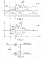
- FIG. 4 illustrates a graph 400 showing curves 402, 404 and 406, respectively corresponding to the Vca, Vcb and Vcc capacitor voltage feedback signals 119.
- a graph 500 and FIG. 5 illustrates filter output current waveforms 502, 504 and 506 corresponding to the first inductor currents I1a, I1b and I1c.
- the controller 120 turns on the single selected rectifier switching device (e.g., Q1) at time T1 (at 306 in FIG.
- the single selected rectifier switching device e.g., Q1
- the controller 120 turns on the selected switch for a non-zero time T1 - T2.
- the controller 120 measures the filter voltage and/or current associated with the selected rectifier switch at 310.
- the controller 120 determines the resonant frequency ⁇ res based on the transient response of the measured voltage or current signal using any suitable techniques.
- the resonance detection and impedance computation component 122 includes program instructions to implement Fast Fourier Transform (FFT), zero crossing, filtering and/or peak detection computations based on digital values corresponding to the measured waveform or waveforms 402, 404, 406, 502, 504 and/or 506 to determine the resonant frequency ⁇ res .
- FFT Fast Fourier Transform
- the resonant frequency ⁇ res is the reciprocal of a discernible period in the oscillations of the associated voltage and/or current signals corresponding to the selected actuated switch Q1.
- the controller 120 Based on the equivalent circuit (e.g., FIG. 6 ) of the system corresponding to the Q1 pulse, the controller 120 computes a line impedance (e.g., line inductance) based on the resonant frequency ⁇ res at 314.
- the controller 120 may repeat the process for one or more of the remaining feeder line pairs by selectively pulsing another selected one of the rectifier switching devices Q2-Q5.
- a determination is made at 316 by the controller 120 as to whether all pairs have been tested. If not (NO at 316), the next switch is selected at 318 and the process 300 returns to 306-314 as previously described.
- the detection and computation component 122 may use any suitable technique for algorithm to determine a single resonant frequency value ⁇ res and corresponding line impedance value or values at 312 and 314 based on multiple iterations.
- ⁇ res L R ′ + L 1 L R ′ L 1 C f
- the capacitance value of the DC bus capacitor CDC is ignored, as the capacitance of the DC bus is typically very large and will not affect the oscillatory operation of the filter and grid during resonance at the resonant frequency ⁇ res .
- the impedance computation component 122 includes values for these components stored in the memory 202, and the computation of equation (2) can be performed for each iteration at 306-314 in FIG. 3 .
- the controller 120 selectively adjusts one or more rectifier control parameters to mitigate filter resonance based on the resonant frequency ⁇ res .
- the resonance detection and impedance computation component 122 selectively updates one or more of the voltage and/or current loop PI controller gain values 212, 214, 222 and/or 224 used by the rectifier controller 124 for normal operation of the motor drive system 110 at 320 in FIG. 3 .
- the controller 120 can be programmed or otherwise configured to perform the above described line impedance determination on power up and/or during any standby mode operation.
- the controller 120 is responsive to user initiated resonance detection/impedance computation commands or signals (e.g., from a user interface or external network-connected control system component (not shown) to enter the standby mode and to perform the processing at 304-314 in order to determine the resonant frequency frequency ⁇ res and optionally to compute the line impedance value L LINE .
- user initiated resonance detection/impedance computation commands or signals e.g., from a user interface or external network-connected control system component (not shown) to enter the standby mode and to perform the processing at 304-314 in order to determine the resonant frequency frequency frequency ⁇ res and optionally to compute the line impedance value L LINE .
- the drive 110 enters normal mode operation with the controller 120 implementing normal rectifier switching operation at 322.
- the controller 120 employs the rectifier controller 124 to implement normal AC/DC conversion operation by selectively providing the switching control signals 125 to cause the rectifier 114 to convert AC input power to provide DC output power at the DC output terminals.
- the resonance detection and impedance computation component 122 is implemented by the controller 120 in order to measure one or more filter voltage or current signals or values 119 at 324 while the rectifier 114 is converting AC input power to provide the DC output power.
- the component 122 determines the resonant frequency ⁇ res based on the measured voltage or current signal.
- the controller 120 does not disturb the normal rectifier switching control signals 125 to create false transients in the system. Instead, the controller 120 performs passive monitoring at 324 and 326, and uses measured values to identify potential resonant conditions in the filter circuit 112. In this regard, certain feedback values 119 may provide higher signal/noise ratios for this resonance detection function at 324, 326 than others. For instance, line currents will typically have relatively high amplitude fundamental signal content, whereas the filter capacitor voltages and/or filter capacitor circuit currents may be preferred for the measurement and assessment at 324 and 326 during online operation of the AFE rectifier 114.
- the controller 120 can selectively adjust rectifier control parameters (e.g., the PI proportional and/or integral gain values 212, 214, 222 and/or 224 above) to combat resonance based on the resonant frequency ⁇ res determined at 326.
- rectifier control parameters e.g., the PI proportional and/or integral gain values 212, 214, 222 and/or 224 above
- the controller 120 provides active damping on demand in a real-time, on-line condition of the drive 110.
- switching in or out of new loads on the grid 102 and/or any other grid side impedance dynamics can be accommodated by adaptive control of the rectifier 114 in order to mitigate or avoid resonance.
- the adjustment at 328 can include selectively reducing one or more of the PI controller gains 212, 214, 222 and/or 224 to mitigate filter resonance based on the resonant frequency ⁇ res while the rectifier 114 is converting AC input power to provide the DC output power.
- the controller 120 also measures the amplitude of any such resonant signal during the monitoring at 324, 326, and the adaptive rectifier control adjustment can be proportional (e.g., more PI controller gain reduction based on higher amplitude detected resonance).
- the bandwidth or bandwidths of one or more control loops implemented by the rectifier controller 124 can be selectively reduced in order to avoid control loop operation at frequencies near a detected resonant frequency ⁇ res determined at 326.
Description
- The subject matter disclosed herein relates to power conversion and more specifically to power converters with automatic impedance and resonance detection systems.
- TAKAHIRO SAEKI ET AL: "Robust Active Damping Method for a PWM Converter Operating with an Unknown Inductance on the Power Grid", IEEJ JOURNAL OF INDUSTRY APPLICATIONS, vol. 4, no. 3, pp.277-285 discloses that a PWM converter generally includes a low-pass filter to remove the high-frequency switching currents that flow into the power grid. It is common to suppress the resonance of an LCL filter by feedback control of the capacitor current or voltage. A sensorless active damper, to estimate the capacitor voltage or current of the LCL filter and suppress the high-frequency resonance is proposed.
- TOYAMA K ET AL: "Transient oscillation suppression of input filter voltage and current for current-source three-phase PWM AC/DC converter", POWER CONVERSION CONFERENCE - NAGAOKA 1997, PROCEEDINGS OF THE NAGAOKA, JAPAN 3-6 AUG. 1997, pages 253-258 discloses that in contrast to the voltage-source converter, the current-source PWM AC/DC converter has the LC filter between the source and the converter, which may cause an LC resonance both in steady and transient states. Two suppression schemes of transient oscillation for the current-source three-phase PWM AC/DC converter are proposed. One suppression method is based on the feedback control of the fluctuation component of the capacitor voltage. The other one is based on the open-loop control with the rate limiter of the input current reference.
- It is therefore the object of the present invention to provide an improved power conversion system for mitigating filter resonance, a corresponding method, and a corresponding computer-readable medium.
- This object is solved by the subject matter of the independent claims.
- Preferred embodiments are defined by the dependent claims.
- Various aspects of the present disclosure are now summarized to facilitate a basic understanding of the disclosure, wherein this summary is not an extensive overview of the disclosure, and is intended neither to identify certain elements of the disclosure, nor to delineate the scope thereof. Rather, the primary purpose of this summary is to present various concepts of the disclosure in a simplified form prior to the more detailed description that is presented hereinafter. The present disclosure provides power conversion systems, computer readable mediums and methods to mitigate input filter resonance. A controller operates an active front end (AFE) rectifier in a first mode to turn a single rectifier switching device on and off and measures a filter voltage or current signal while all of the rectifier switches are off. The controller determines a resonant frequency based on a transient response of the measured voltage or current signal, and selectively adjusts a rectifier control parameter to mitigate filter resonance based on the resonant frequency.
-
-
FIG. 1 is a schematic diagram. -
FIG. 2 is a schematic diagram. -
FIG. 3 is a flow diagram. -
FIG. 4 is a signal waveform diagram. -
FIG. 5 is a signal waveform diagram. -
FIG. 6 is a schematic diagram. - Referring now to the figures, several embodiments or implementations are hereinafter described in conjunction with the drawings, wherein like reference numerals are used to refer to like elements throughout, and wherein the various features are not necessarily drawn to scale.
FIG. 1 shows apower system 100 including a three phaseAC power source 102 including a grid connection and associated feeder lines that provide AC input power along phase lines A, B and C to a motor drivepower conversion system 110 to drive amotor load 104. Thepower conversion system 110 includes a three phaseinput filter circuit 112 that delivers AC power along lines U, V and W to the input of a three-phase active front end (AFE)rectifier 114. Thefilter circuit 112 includesactive damping circuitry 118, and thedrive 110 includes a damping control circuit orcontroller 120. Therectifier 114 has an input to receive AC input power along the lines U, V and W, and an output to provide a DC output signal. An intermediate DC circuit or DC bus is connected between the DC output of therectifier 114 and the input of anoutput inverter 116. In one example, the DC intermediate circuit includes a capacitor CDC connected between positive and negative DC bus lines DC+ and DC- as shown inFIG. 1 . In other examples, a current source converter implementation of themotor drive 110 includes one or more DC link chokes or inductors in the intermediate circuit between the output of therectifier 114 and the inverter input. Theinverter 116 inFIG. 1 includes a DC input coupled to the output of therectifier 114 through the intermediate circuit, and an output coupleable to themotor load 104 to provide an AC output signal. In this example, theinverter 116 provides a three-phase output signal to drive themotor load 104. In other examples, a single phase AC output signal can be provided by the output of theinverter 116 to drive aload 104. TheAFE rectifier 114 can provide DC input power to any suitable load or loads. In the example ofFIG. 1 , thesystem 110 includes asingle inverter 116 operated by aninverter controller 126 to drive asingle motor load 104. In other examples, theAFE rectifier 114 and thefilter circuit 112 can be used in a multi-drive configuration to provide DC input power to multiple loads, such as a plurality ofinverters 116 individually driving aseparate motor load 104. Such a system can be provided in a multi-bay enclosure with common DC bus connections to provide power from therectifier 114 to a plurality ofinverters 116. - The
power conversion system 110 can use a variety of different input filter topologies orconfigurations 112. For example, an inductor - capacitor (LC) or inductor - capacitor - inductor (LCL) input filter circuit can be associated with each AC input phase A/U, B/V, C/W to control the harmonic content of a connected power grid. For example, LCL or LC filters may be used in voltage source converters, such as themotor drive 110 ofFIG. 1 , and LC filters can be used with current source converters. Such filter circuits are subject to damage or degradation of the filter capacitors, such as by voltage surges or other transients, as well as degradation due to isolation of thefilter circuit 112 and resonance. Filter capacitor degradation, in turn, may be costly in terms of replacement component costs, labor for inspection and replacement, as well as downtime for the power conversion system and any associated machinery. Theinput filter 112 can resonate, particularly at startup of theAFE rectifier 114 where the operation of therectifier 114 and associated closed loop control loops implemented by therectifier 114 have bandwidths including resonant frequencies of the input rectifier and the associatedgrid 102. In addition, filter resonance can occur when the line impedance of the grid and feeder lines of thesource 102 changes, for example, when another system on the grid is powered up or down. - The illustrated
system 110 includes acontroller 120 with one or more processors and associated electronic memory with program instructions to mitigate input filter resonance. Thecontroller 120 includes a rectifier control component orsystem 124 providing rectifierswitching control signals 125 to IGBTs or other switches of therectifier 114 to operate theAFE rectifier 114. Thecontroller 120 also includes or implements an inverter control component orsystem 126 to provide inverterswitching control signals 127 to operate theinverter 116. Thecontroller 120 operates themotor drive 110 in various operational modes. In a first or standby mode, a resonance detection andimpedance computation component 122 causes therectifier controller 124 to actuate individual AFE switches to short circuit pairs of feeder lines for a non-zero time period while theinverter 116 is off. This induces a transient reaction by the impedance components of thefilter 112 and thesource 102. Following the pulsed transient event, thecontroller 120 obtains measurements of one or more filter voltages or currents via one or more feedback signals orvalues 119 from afeedback system 118 associated with theinput filter 112 to evaluate transient response while all the rectifier and inverter switches are off. Thecontroller 120 determines a resonant frequency ωres based on the transient response of the measured voltage or current signal, and selectively adjusts one or more control parameters of therectifier controller 124 to mitigate filter resonance based on the resonant frequency ωres. In various implementations, any combination of feedback signals can be used to determine the resonance frequency ωres and/or to determine line impedance, including without limitation I1abc, I2abc, Vcabc, Ifabc or combinations thereof. -
FIG. 2 shows further details of an exampleLCL filter circuit 112 in thepower converter 110. Each phase of the grid andfeeder line source 102 provides a line impedance ZLlNE, and the source delivers grid voltages Vga, Vgb and Vgc. TheLCL filter circuit 112 includes first and second filter inductors L1 and L2 connected between the input of therectifier 114 and the output of thesource 102 for each phase A/U, B/V and C/W. The phase A/U of thefilter 112 includes a first (rectifier side) inductor represented as an inductance L1a and a corresponding resistance R1a, as well as a second (grid side) inductor represented as an inductance L2a and a resistance R2a. Similarly, the filter phase B/V includes first and second inductors represented by inductances L1b, L2b and corresponding resistances R1b and R2b, and the filter phase C/W includes first and second inductors represented by inductances L1c, L2c and corresponding resistances R1c and R2c as shown inFIG. 2 . Between the first and second inductors L1 and L2 of each phase line of thefilter 112, a filter capacitor Cf is connected from the line joining the corresponding inductors L1 and L2 to a filter neutral N1. (Illustrated in the drawing as filter capacitors Cfa, Cfb and Cfc in series with corresponding damping resistances Rds, Rdb and Rdc which can be the equivalent series resistance (ESR) of the corresponding filter capacitor Cf or the combination of this ESR with an added separate damping resistor in the filter circuit 112). The filter neutral N1 can, but need not, be connected to the source neutral N. In other examples, the filter capacitors Cf can be connected and a L2 configuration, and thefeedback system 118 can include current sensors for sensing currents through the delta-connected filter capacitors or currents flowing into the filter capacitor circuit branches, as well as voltage sensors for sensing the voltages across the delta-connected capacitors or line-line voltages between the filter capacitor circuit branches. - The feedback circuit or
system 118 includes one or more sensors (not shown) to sense or detect one or more electrical conditions in thefilter circuit 112. Thefeedback circuit 118 provides one or more feedback signals or values 119 (e.g., analog signals and/or converted digital values) to thecontroller 120 for use in closed loop feedback control of themotor drive 110 generally, as well as for use by the resonance detection andimpedance computation component 122. In one example, thefeedback circuit 118 includes current sensors to provide one or more signals or digital values representing filter input phase currents I2a, I2b and I2c representing the current flowing in the second inductors L2. Thefeedback circuit 118 can also include current sensors (not shown) to provide signals or values representing the filter output phase currents flowing through the first inductor L1 of each phase, including currents I1a, I1b and I1c (I1a,b,c). Thefeedback circuit 118 can also include current sensors (not shown) to provide signals or values representing the filter capacitor currents Ifa, Ifb and Ifc (Ifa,b,c) flowing into the filter capacitors Cf. In certain examples, moreover, thefeedback circuit 118 can provide one or more signals orvalues 119 representing the filter capacitor voltages Vca, Vcb and Vcc (Vca,b,c). - As further shown in
FIG. 2 , the rectifier in one example is a switching rectifier with IGBT type switching devices Q1-Q6 individually coupled between a corresponding one of the AC input terminals U, V or W and one of the first and second DC output terminals DC+ or DC-. Other semiconductor-based switching devices can be used, including without limitation field effect transistors (FETs), etc. Each switching devices Q1-Q6 is operated by a corresponding rectifier switching control signal 125 from therectifier controller 124 of thecontrol circuit 120 to selectively connect or disconnect the corresponding AC input terminal to the corresponding DC output terminal. - The
controller 120 and therectifier controller 124 thereof operate the switchingrectifier 114 in various different modes, including a standby mode and a second or normal operating mode. For instance, on power up of thepower conversion system 110, thecontroller 120 operates in a standby mode in order to facilitate precharging of the DC bus capacitance CDC, for example, using a dedicated precharging circuit (not shown). During the standby operation, the inverter (FIG. 1 ) is turned off. Thecontroller 120 also operates therectifier 114 in a second or normal mode, in which therectifier controller 124 provides the rectifierswitching control signals 125 using pulse width modulation according to any suitable control schemes (e.g., space vector modulation or SVM, selective harmonic elimination or SHE, etc.) in order to cause therectifier 114 to convert AC input power from the output of thefilter circuit 120 to provide DC output power to the intermediate DC bus circuit (CDC) and a connected load (e.g., one ormore inverters 116 inFIG. 1 ). - As further shown in
FIG. 2 , thecontroller 120 in one example includes aprocessor 200 operatively coupled with an associatedelectronic memory 202. Thecontroller 120 and the components thereof may be any suitable hardware, processor-executed software, processor-executed firmware, logic, or combinations thereof that are adapted, programmed, or otherwise configured to implement the functions illustrated and described herein. Thecontroller 120 in certain embodiments may be implemented, in whole or in part, as software components executed using one or more processing elements, such as one ormore processors 200, and may be implemented as a set of sub-components or objects including computer executable instructions stored in the non-transitory computer readableelectronic memory 202 for operation using computer readable data executing on one or more hardware platforms such as one or more computers including one or more processors, data stores, memory, etc. The components of thecontroller 120 may be executed on the same computer processor or in distributed fashion in two or more processing components that are operatively coupled with one another to provide the functionality and operation described herein. - The
controller 120 in one example is configured by execution in theprocessor 200 of instructions in thememory 202 to implement various motor drive functions as are known, as well as resonance detection and impedance computation functionality via thecomponent 122 provided as a component including processor-executable instructions in thememory 202 in one example. Similarly, the rectifier control functions can be implemented at least in part via processorexecutable instructions 124 stored in thememory 202 for execution by theprocessor 200. In addition, thecontroller 120 can include various signal conditioning circuits for receiving and converting analog signals into digital signals, and for providing suitable output signals (e.g., rectifierswitching control signals 125 and inverter switching control signals 127 (FIG. 1 ) suitable for operating the various switching devices of therectifier 114 and theinverter 116. - The
rectifier controller component 124 in one example implements multiple control loops in normal operation to cause the switchingrectifier 114 to convert AC input power to provide DC output power. In the example ofFIG. 2 , therectifier controller 124 includes a voltage control loop proportional-integral control component (PI controller) 210 operating on one or more voltage feedback signals (e.g., measured or computed DC bus voltage feedback value) and voltage setpoint values (e.g., setpoint or desired DC bus voltage value) that apply a proportional gain value 212 (KP-V) and an integral gain value 214 (KI-V) to a voltage error signal to compute one or more voltage control output signals or values for use in generating the rectifier switching control signals 125. In addition, therectifier controller 124 implements a current controlloop PI controller 220 with a proportional gain value 222 (KP-I) and an integral gain value 224 (KI-I). Thecurrent PI controller 220 operates on one or more current setpoint values and feedback values in order to compute a current control output signal or value also used in generating the rectifier switching control signals 125. Thecontroller 120 also implements the resonance detection andimpedance computation component 122 which operates in conjunction with therectifier controller 124 to perform various functions detailed herein in operation of thecontroller 120 in a first (e.g., standby or startup) mode and in a second (e.g., normal) mode. - Referring also to
FIG. 3 , amethod 300 illustrates an example process or method for operating the motor drivepower conversion system 110 to mitigate resonance conditions in thefilter circuit 112. In one example, themethod 300 is implemented by thecontroller 120 ofFIGs. 1 and2 . The drive is powered up at 302, and operation begins in the first or standby mode with therectifier 114 and theinverter 116 off (e.g., all switches open). At 304, thecontroller 120 operates suitable precharging circuitry (not shown) to precharged the DC bus capacitor or capacitor CDC to a suitable level while therectifier 114 andinverter 116 remain off. While still in the first mode with the inverter switches off, thecontroller 120 implements the resonance detection andimpedance computation component 122 together with therectifier controller 124 in order to turn on a single selected rectifier switch (e.g., Q1) while keeping the other rectifier switching devices (e.g., Q2-Q6) off at 306. For example, closing the upper switch Q1 when Vgc is greater than Vga causes current to flow from the node W through the upper diode of Q5 and back through the switch Q1. At 308, thecomponent 122 causes therectifier controller 124 to turn off the selected rectifier switching device Q1, while still maintaining the other rectifier switching devices Q2-Q6 off. In one example, thecontroller 120 provides apulse signal 125 to the selected rectifier switching device Q1 at 306 and 308 in order to selectively short a pair of feeder lines of thesource 102 for a predetermined time. - At 310, following the predetermined time period, the
controller 120 assesses one or more feedback signals 119 to measure one or more filter voltages or currents associated with the selected rectifier switch Q1. In this example, turning on Q1 allows current to flow through the flyback diodes of one or both of rectifier input lines A the and/or W to the upper DC bus line DC+, and back through the switching device Q1. Since a current flow path is provided through thefilter circuit 120 and theAC input source 102, the transient pulse created at 306 and 308 will cause the resonant circuit to undergo a transient response. In particular, the circuit will exhibit resonant behavior at a resonant frequency corresponding to the impedances of the line (e.g.,source 102 including the grid and any feeder lines) and the components of thefilter circuit 112. -
FIG. 6 illustrates anequivalent circuit 600 for this circuit configuration following a pull supplied by turning on Q1 in therectifier 114 ofFIG. 2 . As seen inFIG. 6 , the DC bus capacitor CDC is connected to the first inductors L1c and L1a, and the corresponding filter capacitors Cfc and Cfa of thefilter circuit 112, as well as grid inductances LGc and The respective grid inductances L1c and L1a in this case are the sum of the second (grid side) inductors L2c, L2a and the corresponding line inductances LLINEc and LLINEa (of the line impedances ZLINE shown inFIG. 1 ). For example, LGc in this example = L2c + LLINEc, and LGa = L2a + LLINEa. - Referring also to
FIGs. 4 and 5 , thecontroller 120 determines a resonant frequency ωres based on the transient response of the measured voltage or current signal at 312 inFIG. 3 .FIG. 4 illustrates a graph 400 showingcurves graph 500 andFIG. 5 illustrates filter outputcurrent waveforms graphs 400 and 500, thecontroller 120 turns on the single selected rectifier switching device (e.g., Q1) at time T1 (at 306 inFIG. 3 ), and then turns off the selected switch at time T2 (at 308). As can be seen in the voltage andcurrent graphs 400 and 500, thecontroller 120 turns on the selected switch for a non-zero time T1 - T2. After the selected switch is again turned off at T2, thecontroller 120 measures the filter voltage and/or current associated with the selected rectifier switch at 310. At 312, thecontroller 120 determines the resonant frequency ωres based on the transient response of the measured voltage or current signal using any suitable techniques. In one example, the resonance detection andimpedance computation component 122 includes program instructions to implement Fast Fourier Transform (FFT), zero crossing, filtering and/or peak detection computations based on digital values corresponding to the measured waveform orwaveforms FIGs. 4 and 5 , for example, the resonant frequency ωres is the reciprocal of a discernible period in the oscillations of the associated voltage and/or current signals corresponding to the selected actuated switch Q1. - Based on the equivalent circuit (e.g.,
FIG. 6 ) of the system corresponding to the Q1 pulse, thecontroller 120 computes a line impedance (e.g., line inductance) based on the resonant frequency ωres at 314. Thecontroller 120 may repeat the process for one or more of the remaining feeder line pairs by selectively pulsing another selected one of the rectifier switching devices Q2-Q5. In the example ofFIG. 3 , a determination is made at 316 by thecontroller 120 as to whether all pairs have been tested. If not (NO at 316), the next switch is selected at 318 and theprocess 300 returns to 306-314 as previously described. If more than one iteration is implemented, the detection andcomputation component 122 may use any suitable technique for algorithm to determine a single resonant frequency value ωres and corresponding line impedance value or values at 312 and 314 based on multiple iterations. - The resonant frequency value ωres in one example is given by the following equation (1):

where Lg is the initially unknown grid inductance value including the grid side filter inductor L2 (e.g., Lg = L2 + LLINE ). In this approach, the capacitance value of the DC bus capacitor CDC is ignored, as the capacitance of the DC bus is typically very large and will not affect the oscillatory operation of the filter and grid during resonance at the resonant frequency ωres. Thecontroller 120 in one example computes the line impedance value LLINE at 314 according to the following equation (2):
- Since the inductance and capacitance values of the filter circuit components are known, the
impedance computation component 122 includes values for these components stored in thememory 202, and the computation of equation (2) can be performed for each iteration at 306-314 inFIG. 3 . - At 320, the
controller 120 selectively adjusts one or more rectifier control parameters to mitigate filter resonance based on the resonant frequency ωres. In one example, the resonance detection andimpedance computation component 122 selectively updates one or more of the voltage and/or current loop PI controller gain values 212, 214, 222 and/or 224 used by therectifier controller 124 for normal operation of themotor drive system 110 at 320 inFIG. 3 . In this regard, thecontroller 120 can be programmed or otherwise configured to perform the above described line impedance determination on power up and/or during any standby mode operation. In certain embodiments, moreover, thecontroller 120 is responsive to user initiated resonance detection/impedance computation commands or signals (e.g., from a user interface or external network-connected control system component (not shown) to enter the standby mode and to perform the processing at 304-314 in order to determine the resonant frequency frequency ωres and optionally to compute the line impedance value LLINE. - Returning to
FIG. 3 , thedrive 110 enters normal mode operation with thecontroller 120 implementing normal rectifier switching operation at 322. In this second operating mode, thecontroller 120 employs therectifier controller 124 to implement normal AC/DC conversion operation by selectively providing theswitching control signals 125 to cause therectifier 114 to convert AC input power to provide DC output power at the DC output terminals. During this normal switching operation, the resonance detection andimpedance computation component 122 is implemented by thecontroller 120 in order to measure one or more filter voltage or current signals orvalues 119 at 324 while therectifier 114 is converting AC input power to provide the DC output power. At 326, thecomponent 122 determines the resonant frequency ωres based on the measured voltage or current signal. This is unlike intrusive on-line approaches for resonance detection and/or impedance measurements, since thecontroller 120 does not disturb the normal rectifierswitching control signals 125 to create false transients in the system. Instead, thecontroller 120 performs passive monitoring at 324 and 326, and uses measured values to identify potential resonant conditions in thefilter circuit 112. In this regard, certain feedback values 119 may provide higher signal/noise ratios for this resonance detection function at 324, 326 than others. For instance, line currents will typically have relatively high amplitude fundamental signal content, whereas the filter capacitor voltages and/or filter capacitor circuit currents may be preferred for the measurement and assessment at 324 and 326 during online operation of theAFE rectifier 114. - At 328, the
controller 120 can selectively adjust rectifier control parameters (e.g., the PI proportional and/or integral gain values 212, 214, 222 and/or 224 above) to combat resonance based on the resonant frequency ωres determined at 326. In this manner, thecontroller 120 provides active damping on demand in a real-time, on-line condition of thedrive 110. As a result, switching in or out of new loads on thegrid 102 and/or any other grid side impedance dynamics can be accommodated by adaptive control of therectifier 114 in order to mitigate or avoid resonance. For instance, the adjustment at 328 (and the adjustment at 320 above) can include selectively reducing one or more of the PI controller gains 212, 214, 222 and/or 224 to mitigate filter resonance based on the resonant frequency ωres while therectifier 114 is converting AC input power to provide the DC output power. In one example, thecontroller 120 also measures the amplitude of any such resonant signal during the monitoring at 324, 326, and the adaptive rectifier control adjustment can be proportional (e.g., more PI controller gain reduction based on higher amplitude detected resonance). In this manner, the bandwidth or bandwidths of one or more control loops implemented by the rectifier controller 124 (e.g., voltage and/orcurrent control loops 210, 220) can be selectively reduced in order to avoid control loop operation at frequencies near a detected resonant frequency ωres determined at 326. - In the preceding specification, various embodiments have been described with reference to the accompanying drawings. It will, however, be evident that various modifications and changes may be made thereto, and additional embodiments may be implemented, without departing from the broader scope of the invention as set forth in the claims that follow. The specification and drawings are accordingly to be regarded in an illustrative rather than restrictive sense.
Claims (15)
- A power conversion system (110), comprising:an AC input coupleable to receive AC input power from a power source (102);a rectifier (114), including a plurality of AC input terminals (U, V, W), first and second DC output terminals (DC+, DC-), and a plurality of switching devices (Q1, ..., Q6) individually coupled between a corresponding one of the AC input terminals and one of the first and second DC output terminals;a filter circuit (112) coupled between the AC input and the rectifier; anda controller (120) to provide switching control signals (125) to operate the switching devices of the rectifier, the controller operative in a first mode to:turn (306) a single one (Q1) of the switching devices on for a non-zero time period in order to short a pair of feeder lines (A, C) connected with the power source (102),turn (308) the single one of the switching devices off after the non-zero time period,measure (310) a voltage (Vca,b,c) or current signal (I1a,b,c; Ifa,b,c) associated with the filter circuit while all of the switching devices (Q1, ..., Q6) are off after the non-zero time period,determine (312) a resonant frequency (ωres) based on a transient response of the measured voltage or current signal, andselectively adjust (320) a rectifier control parameter to mitigate filter resonance based on the resonant frequency.
- The power conversion system of claim 1, wherein the controller is further operative to compute a line impedance associated with the power source based on the resonant frequency.
- The power conversion system of claim 1 or 2, wherein the controller is operative in a second mode to:selectively provide the switching control signals to cause the rectifier to convert AC input power to provide DC output power at the DC output terminals;measure (324) the voltage or current signal associated with the filter circuit while the rectifier is converting AC input power to provide the DC output power;determine (326) the resonant frequency based on the measured voltage or current signal; andselectively adjust (328) the rectifier control parameter to mitigate filter resonance based on the resonant frequency while the rectifier is converting AC input power to provide the DC output power.
- The power conversion system of claim 3, wherein the controller is operative in the first and second modes to selectively adjust the rectifier control parameter to reduce a control loop bandwidth based on the resonant frequency.
- The power conversion system of one of claims 1 to 4, wherein the controller is operative in the first mode to selectively adjust the rectifier control parameter to reduce a control loop bandwidth based on the resonant frequency.
- The power conversion system of one of claims 1 to 5, wherein the controller is operative after the power conversion system is initially powered up to precharge a DC bus capacitor (CDC) at the output of the rectifier before turning the single one of the switching devices on for the non-zero time period.
- The power conversion system of one of claims 1 to 6, wherein the controller is operative to:individually turn each of the switching devices on and off and measure the voltage or current signal to determine a corresponding resonant frequency in the first mode;determine a plurality of resonant frequencies based on a transient response of the measured voltage or current signal individually corresponding to the plurality of switching devices; andselectively adjust a rectifier control parameter to mitigate filter resonance based on at least one of the plurality of resonant frequencies.
- The power conversion system of claim 7, wherein the controller is further operative to compute a line impedance associated with the power source based on at least one of the plurality of resonant frequencies.
- The power conversion system of claim 7, wherein the controller is operative in a second mode to:selectively provide the switching control signals to cause the rectifier to convert AC input power to provide DC output power at the DC output terminals;measure the voltage or current signal associated with the filter circuit while the rectifier is converting AC input power to provide the DC output power;determine the resonant frequency based on the measured voltage or current signal; andselectively adjust the rectifier control parameter to mitigate filter resonance based on the resonant frequency while the rectifier is converting AC input power to provide the DC output power; and/orwherein the controller is operative in the first and second modes to selectively adjust the rectifier control parameter to reduce a control loop bandwidth based on the resonant frequency.
- A method (300) to mitigate resonance in a filter (112) for delivering AC power to a rectifier of a power conversion system (110), the method comprising, in a first operating mode:turning (306) a single one (Q1) of a plurality of rectifier switching devices (Q1, ..., Q6) on for a non-zero time period in order to short a pair of feeder lines (A, C) connected with a power source (102);turning (308) the single one of the rectifier switching devices off after the non-zero time period;measuring (310) a voltage (Vca,b,c) or current signal (I1a,b,c; Ifa,b,c) associated with the filter circuit while all of the plurality of switching devices (Q1, ..., Q6) are off after the non-zero time period,determining (312) a resonant frequency (ωres) based on a transient response of the measured voltage or current signal; andselectively adjusting (320) a rectifier control parameter to mitigate filter resonance based on the resonant frequency.
- The method of claim 10, further comprising, in the first operating mode, computing a line impedance associated with the power source based on the resonant frequency.
- The method of claim 10 or 11, further comprising, in a second mode:selectively providing switching control signals to cause a rectifier (114) to convert AC input power to provide DC output power;measuring (324) the voltage or current signal associated with the filter circuit while the rectifier is converting AC input power to DC output power;determining (326) the resonant frequency based on the measured voltage or current signal; andselectively adjusting (328) the rectifier control parameter to mitigate filter resonance based on the resonant frequency while the rectifier is converting AC input power to DC output power; and/orfurther comprising, in the first and second modes, selectively adjusting the rectifier control parameter to reduce a control loop bandwidth based on the resonant frequency.
- The method of one of claims 10 to 12, further comprising, in the first mode, selectively adjusting the rectifier control parameter to reduce a control loop bandwidth based on the resonant frequency; or
further comprising, after the power conversion system is initially powered up, precharging a DC bus capacitor (DCD) at the output of the rectifier before turning the single one of the switching devices on for the non-zero time period; or
further comprising:individually turning each of the switching devices on and off and measure the voltage or current signal to determine a corresponding resonant frequency in the first mode;determining a plurality of resonant frequencies based on a transient response of the measured voltage or current signal individually corresponding to the plurality of switching devices; andselectively adjusting a rectifier control parameter to mitigate filter resonance based on at least one of the plurality of resonant frequencies. - A non-transitory computer readable medium with computer executable instructions for mitigating resonance in a filter (112) for delivering AC power to a rectifier of a power conversion system (110), the computer readable medium comprising computer executable instructions which when executed on a controller of a power conversion system according to claim 1 carry out the method steps according to claim 10.
- The non-transitory computer readable medium of claim 14, further comprising, computer executable instructions for, in a second mode:selectively providing switching control signals to cause a rectifier (114) to convert AC input power to provide DC output power;measuring (324) the voltage or current signal associated with the filter circuit while the rectifier is converting AC input power to DC output power;determining (326) the resonant frequency based on the measured voltage or current signal; andselectively adjusting (328) the rectifier control parameter to mitigate filter resonance based on the resonant frequency while the rectifier is converting AC input power to DC output power; orfurther comprising, computer executable instructions for, in the first mode, selectively adjusting the rectifier control parameter to reduce a control loop bandwidth based on the resonant frequency.
Applications Claiming Priority (1)
| Application Number | Priority Date | Filing Date | Title |
|---|---|---|---|
| US15/173,767 US9960723B2 (en) | 2016-06-06 | 2016-06-06 | Motor drive with resonance detection and impedance computation |
Publications (2)
| Publication Number | Publication Date |
|---|---|
| EP3258581A1 EP3258581A1 (en) | 2017-12-20 |
| EP3258581B1 true EP3258581B1 (en) | 2019-01-23 |
Family
ID=58873661
Family Applications (1)
| Application Number | Title | Priority Date | Filing Date |
|---|---|---|---|
| EP17173409.8A Active EP3258581B1 (en) | 2016-06-06 | 2017-05-30 | Motor drive with resonance detection and impedance computation |
Country Status (3)
| Country | Link |
|---|---|
| US (1) | US9960723B2 (en) |
| EP (1) | EP3258581B1 (en) |
| CN (1) | CN107834877B (en) |
Families Citing this family (13)
| Publication number | Priority date | Publication date | Assignee | Title |
|---|---|---|---|---|
| DE102014219278A1 (en) * | 2014-09-24 | 2016-03-24 | Bombardier Transportation Gmbh | Method and device for monitoring an electrical network in a rail vehicle and rail vehicle |
| DE102016224472A1 (en) * | 2016-12-08 | 2018-06-14 | Audi Ag | Converter device for a motor vehicle and motor vehicle |
| US10158299B1 (en) * | 2018-04-18 | 2018-12-18 | Rockwell Automation Technologies, Inc. | Common voltage reduction for active front end drives |
| US10615705B1 (en) * | 2018-12-27 | 2020-04-07 | Rockwell Automation Technologies, Inc. | Power converter control system observer |
| CN109687754B (en) * | 2019-01-30 | 2020-07-24 | 东北电力大学 | Self-adaptive three-phase L C L grid-connected inverter control method |
| US10686376B1 (en) | 2019-05-06 | 2020-06-16 | Hamilton Sunstrand Corporation | Method and system for control of tunable passive component based power filters |
| US11211879B2 (en) | 2019-09-23 | 2021-12-28 | Rockwell Automation Technologies, Inc. | Capacitor size reduction and lifetime extension for cascaded H-bridge drives |
| CN113933679A (en) * | 2020-06-29 | 2022-01-14 | 株洲中车时代电气股份有限公司 | Parameter monitoring method and device for locomotive converter circuit |
| JP7408500B2 (en) | 2020-07-16 | 2024-01-05 | 東芝エネルギーシステムズ株式会社 | power converter |
| US11336206B2 (en) * | 2020-09-23 | 2022-05-17 | Rockwell Automation Technoligies, Inc. | Switching frequency and PWM control to extend power converter lifetime |
| CN113315443B (en) * | 2021-05-14 | 2023-02-07 | 苏州汇川联合动力系统有限公司 | Three-electric-system resonance point identification method, motor controller and storage medium |
| CN113381592B (en) * | 2021-05-14 | 2023-03-14 | 西安理工大学 | Method for solving capacitive current feedback coefficient of inverter self-adaptive resonance suppression |
| CN113671257B (en) * | 2021-08-12 | 2022-10-04 | 合肥工业大学 | Impedance measurement method for switching disturbance mode |
Family Cites Families (16)
| Publication number | Priority date | Publication date | Assignee | Title |
|---|---|---|---|---|
| US5367448A (en) | 1992-08-07 | 1994-11-22 | Carroll Lawrence B | Three phase AC to DC power converter |
| EP1339153B1 (en) | 2002-02-19 | 2011-10-05 | Fraunhofer-Gesellschaft zur Förderung der angewandten Forschung e.V. | Device for connecting a building or similar to a low voltage electric network |
| US7164275B2 (en) | 2004-09-30 | 2007-01-16 | Rockwell Automation Technologies, Inc. | AC power line impedance monitoring method and system |
| JP4082438B2 (en) | 2006-08-30 | 2008-04-30 | ダイキン工業株式会社 | Current-controlled power converter |
| JP5259077B2 (en) | 2006-12-04 | 2013-08-07 | 株式会社京三製作所 | Instantaneous voltage drop compensation circuit, power converter, instantaneous voltage drop compensation method, and instantaneous voltage drop compensation program |
| JP5504878B2 (en) | 2009-12-24 | 2014-05-28 | 株式会社デンソー | Vehicle generator |
| US8259426B2 (en) | 2010-05-28 | 2012-09-04 | Rockwell Automation Technologies, Inc. | Variable frequency drive and methods for filter capacitor fault detection |
| CN103026572B (en) | 2010-07-23 | 2015-07-01 | Abb技术有限公司 | Method and arrangement for capacitor bank protection |
| RU2563321C2 (en) | 2011-02-16 | 2015-09-20 | Абб Рисерч Лтд | Method and assembly for detection of inner fault in y-y-connected bank of capacitors |
| US8570775B2 (en) * | 2011-02-17 | 2013-10-29 | Rockwell Automation Technologies, Inc. | CMV reduction under bus transient condition |
| US9667128B2 (en) * | 2012-04-30 | 2017-05-30 | Rockwell Automation Technologies, Inc. | Power converter resonance detection apparatus and method |
| CN102710105B (en) * | 2012-05-30 | 2014-09-24 | 电子科技大学 | Active damping control device for LCL filtering PWM current converter |
| JP2015186431A (en) * | 2014-03-26 | 2015-10-22 | 株式会社安川電機 | Power converter, controller for power converter, and control method for power converter |
| JP2015201996A (en) | 2014-04-09 | 2015-11-12 | 株式会社安川電機 | Power conversion device, control device for power conversion device, and control method for power conversion device |
| US9787212B2 (en) * | 2014-05-05 | 2017-10-10 | Rockwell Automation Technologies, Inc. | Motor drive with silicon carbide MOSFET switches |
| CN104836232B (en) * | 2015-05-14 | 2017-02-01 | 电子科技大学 | Frequency wide-range self-adaptive repetition control method of active power filter |
-
2016
- 2016-06-06 US US15/173,767 patent/US9960723B2/en active Active
-
2017
- 2017-05-26 CN CN201710384933.9A patent/CN107834877B/en active Active
- 2017-05-30 EP EP17173409.8A patent/EP3258581B1/en active Active
Non-Patent Citations (1)
| Title |
|---|
| None * |
Also Published As
| Publication number | Publication date |
|---|---|
| EP3258581A1 (en) | 2017-12-20 |
| US9960723B2 (en) | 2018-05-01 |
| US20170353138A1 (en) | 2017-12-07 |
| CN107834877A (en) | 2018-03-23 |
| CN107834877B (en) | 2020-01-10 |
Similar Documents
| Publication | Publication Date | Title |
|---|---|---|
| EP3258581B1 (en) | Motor drive with resonance detection and impedance computation | |
| US10263558B2 (en) | Phase loss detection in active front end converters | |
| US10644614B2 (en) | Conversion device having a control unit for detecting arm short-circuit | |
| EP2166635A1 (en) | Current measurement in an inverter unit and a frequency converter | |
| US10536071B2 (en) | Detecting ground faults on non-isolated DC systems | |
| CN106505840B (en) | A kind of grid-connected photovoltaic inverter harmonic wave management method | |
| EP3637115B1 (en) | Method and apparatus for detecting capacitance value of filter capacitor in inverter | |
| EP3637574B1 (en) | Method for estimating electrical parameters of a grid | |
| EP3588726A1 (en) | Neutral connection detection method for 3/4 -wire active filters | |
| US20180006581A1 (en) | Voltage converting device and wireless power transmitting device | |
| CN109716609B (en) | Method for phase-controlled excitation of a power transformer | |
| JP4849310B2 (en) | AC / AC power converter controller | |
| US9581649B2 (en) | Method and apparatus for load fault detection | |
| EP3096429B1 (en) | Identification of lcl filter parameters | |
| JP2007124816A (en) | Controller for ac/ac power converter | |
| US10972031B2 (en) | Active stabilization of DC link in motor drive systems | |
| JP2009290938A (en) | Inverter apparatus and method of measuring its noise | |
| US10725116B2 (en) | Automatic system grounding condition detection | |
| US20190260311A1 (en) | Uncertainty Based Controller Design for an Inverter | |
| JP2017169417A (en) | Diode rectification switching power supply device, on-vehicle device, and ringing suppression method | |
| US11162988B2 (en) | Load impedance tester and measurement method | |
| KR20180078871A (en) | An automatic method of limiting the output voltage ripple for switching power supply | |
| JPH11341684A (en) | Voltage sensing type active filter | |
| JP2020048400A (en) | Short circuit detection device for filter circuit | |
| Lovell | Time-domain Parameter Estimation for Fault Identification in a Current-source Push-pull Parallel Resonant Inverter |
Legal Events
| Date | Code | Title | Description |
|---|---|---|---|
| PUAI | Public reference made under article 153(3) epc to a published international application that has entered the european phase |
Free format text: ORIGINAL CODE: 0009012 |
|
| STAA | Information on the status of an ep patent application or granted ep patent |
Free format text: STATUS: THE APPLICATION HAS BEEN PUBLISHED |
|
| AK | Designated contracting states |
Kind code of ref document: A1 Designated state(s): AL AT BE BG CH CY CZ DE DK EE ES FI FR GB GR HR HU IE IS IT LI LT LU LV MC MK MT NL NO PL PT RO RS SE SI SK SM TR |
|
| AX | Request for extension of the european patent |
Extension state: BA ME |
|
| STAA | Information on the status of an ep patent application or granted ep patent |
Free format text: STATUS: REQUEST FOR EXAMINATION WAS MADE |
|
| 17P | Request for examination filed |
Effective date: 20180608 |
|
| RBV | Designated contracting states (corrected) |
Designated state(s): AL AT BE BG CH CY CZ DE DK EE ES FI FR GB GR HR HU IE IS IT LI LT LU LV MC MK MT NL NO PL PT RO RS SE SI SK SM TR |
|
| GRAP | Despatch of communication of intention to grant a patent |
Free format text: ORIGINAL CODE: EPIDOSNIGR1 |
|
| STAA | Information on the status of an ep patent application or granted ep patent |
Free format text: STATUS: GRANT OF PATENT IS INTENDED |
|
| RIC1 | Information provided on ipc code assigned before grant |
Ipc: H02M 1/00 20060101ALN20180813BHEP Ipc: H02M 7/219 20060101ALI20180813BHEP Ipc: H02M 5/458 20060101ALN20180813BHEP Ipc: H02M 1/32 20070101ALI20180813BHEP Ipc: H02M 1/36 20070101ALN20180813BHEP Ipc: H02M 1/12 20060101AFI20180813BHEP |
|
| RIC1 | Information provided on ipc code assigned before grant |
Ipc: H02M 1/00 20060101ALN20180817BHEP Ipc: H02M 5/458 20060101ALN20180817BHEP Ipc: H02M 1/12 20060101AFI20180817BHEP Ipc: H02M 1/36 20070101ALN20180817BHEP Ipc: H02M 1/32 20070101ALI20180817BHEP Ipc: H02M 7/219 20060101ALI20180817BHEP |
|
| INTG | Intention to grant announced |
Effective date: 20180917 |
|
| GRAS | Grant fee paid |
Free format text: ORIGINAL CODE: EPIDOSNIGR3 |
|
| GRAA | (expected) grant |
Free format text: ORIGINAL CODE: 0009210 |
|
| STAA | Information on the status of an ep patent application or granted ep patent |
Free format text: STATUS: THE PATENT HAS BEEN GRANTED |
|
| AK | Designated contracting states |
Kind code of ref document: B1 Designated state(s): AL AT BE BG CH CY CZ DE DK EE ES FI FR GB GR HR HU IE IS IT LI LT LU LV MC MK MT NL NO PL PT RO RS SE SI SK SM TR |
|
| REG | Reference to a national code |
Ref country code: GB Ref legal event code: FG4D |
|
| REG | Reference to a national code |
Ref country code: CH Ref legal event code: EP |
|
| REG | Reference to a national code |
Ref country code: AT Ref legal event code: REF Ref document number: 1092235 Country of ref document: AT Kind code of ref document: T Effective date: 20190215 |
|
| REG | Reference to a national code |
Ref country code: IE Ref legal event code: FG4D |
|
| REG | Reference to a national code |
Ref country code: DE Ref legal event code: R096 Ref document number: 602017001876 Country of ref document: DE |
|
| REG | Reference to a national code |
Ref country code: NL Ref legal event code: MP Effective date: 20190123 |
|
| PG25 | Lapsed in a contracting state [announced via postgrant information from national office to epo] |
Ref country code: NL Free format text: LAPSE BECAUSE OF FAILURE TO SUBMIT A TRANSLATION OF THE DESCRIPTION OR TO PAY THE FEE WITHIN THE PRESCRIBED TIME-LIMIT Effective date: 20190123 |
|
| PG25 | Lapsed in a contracting state [announced via postgrant information from national office to epo] |
Ref country code: NO Free format text: LAPSE BECAUSE OF FAILURE TO SUBMIT A TRANSLATION OF THE DESCRIPTION OR TO PAY THE FEE WITHIN THE PRESCRIBED TIME-LIMIT Effective date: 20190423 Ref country code: FI Free format text: LAPSE BECAUSE OF FAILURE TO SUBMIT A TRANSLATION OF THE DESCRIPTION OR TO PAY THE FEE WITHIN THE PRESCRIBED TIME-LIMIT Effective date: 20190123 Ref country code: SE Free format text: LAPSE BECAUSE OF FAILURE TO SUBMIT A TRANSLATION OF THE DESCRIPTION OR TO PAY THE FEE WITHIN THE PRESCRIBED TIME-LIMIT Effective date: 20190123 Ref country code: ES Free format text: LAPSE BECAUSE OF FAILURE TO SUBMIT A TRANSLATION OF THE DESCRIPTION OR TO PAY THE FEE WITHIN THE PRESCRIBED TIME-LIMIT Effective date: 20190123 Ref country code: PT Free format text: LAPSE BECAUSE OF FAILURE TO SUBMIT A TRANSLATION OF THE DESCRIPTION OR TO PAY THE FEE WITHIN THE PRESCRIBED TIME-LIMIT Effective date: 20190523 Ref country code: LT Free format text: LAPSE BECAUSE OF FAILURE TO SUBMIT A TRANSLATION OF THE DESCRIPTION OR TO PAY THE FEE WITHIN THE PRESCRIBED TIME-LIMIT Effective date: 20190123 Ref country code: PL Free format text: LAPSE BECAUSE OF FAILURE TO SUBMIT A TRANSLATION OF THE DESCRIPTION OR TO PAY THE FEE WITHIN THE PRESCRIBED TIME-LIMIT Effective date: 20190123 |
|
| REG | Reference to a national code |
Ref country code: AT Ref legal event code: MK05 Ref document number: 1092235 Country of ref document: AT Kind code of ref document: T Effective date: 20190123 |
|
| PG25 | Lapsed in a contracting state [announced via postgrant information from national office to epo] |
Ref country code: LV Free format text: LAPSE BECAUSE OF FAILURE TO SUBMIT A TRANSLATION OF THE DESCRIPTION OR TO PAY THE FEE WITHIN THE PRESCRIBED TIME-LIMIT Effective date: 20190123 Ref country code: RS Free format text: LAPSE BECAUSE OF FAILURE TO SUBMIT A TRANSLATION OF THE DESCRIPTION OR TO PAY THE FEE WITHIN THE PRESCRIBED TIME-LIMIT Effective date: 20190123 Ref country code: HR Free format text: LAPSE BECAUSE OF FAILURE TO SUBMIT A TRANSLATION OF THE DESCRIPTION OR TO PAY THE FEE WITHIN THE PRESCRIBED TIME-LIMIT Effective date: 20190123 Ref country code: GR Free format text: LAPSE BECAUSE OF FAILURE TO SUBMIT A TRANSLATION OF THE DESCRIPTION OR TO PAY THE FEE WITHIN THE PRESCRIBED TIME-LIMIT Effective date: 20190424 Ref country code: IS Free format text: LAPSE BECAUSE OF FAILURE TO SUBMIT A TRANSLATION OF THE DESCRIPTION OR TO PAY THE FEE WITHIN THE PRESCRIBED TIME-LIMIT Effective date: 20190523 Ref country code: BG Free format text: LAPSE BECAUSE OF FAILURE TO SUBMIT A TRANSLATION OF THE DESCRIPTION OR TO PAY THE FEE WITHIN THE PRESCRIBED TIME-LIMIT Effective date: 20190423 |
|
| REG | Reference to a national code |
Ref country code: DE Ref legal event code: R097 Ref document number: 602017001876 Country of ref document: DE |
|
| PG25 | Lapsed in a contracting state [announced via postgrant information from national office to epo] |
Ref country code: DK Free format text: LAPSE BECAUSE OF FAILURE TO SUBMIT A TRANSLATION OF THE DESCRIPTION OR TO PAY THE FEE WITHIN THE PRESCRIBED TIME-LIMIT Effective date: 20190123 Ref country code: EE Free format text: LAPSE BECAUSE OF FAILURE TO SUBMIT A TRANSLATION OF THE DESCRIPTION OR TO PAY THE FEE WITHIN THE PRESCRIBED TIME-LIMIT Effective date: 20190123 Ref country code: RO Free format text: LAPSE BECAUSE OF FAILURE TO SUBMIT A TRANSLATION OF THE DESCRIPTION OR TO PAY THE FEE WITHIN THE PRESCRIBED TIME-LIMIT Effective date: 20190123 Ref country code: CZ Free format text: LAPSE BECAUSE OF FAILURE TO SUBMIT A TRANSLATION OF THE DESCRIPTION OR TO PAY THE FEE WITHIN THE PRESCRIBED TIME-LIMIT Effective date: 20190123 Ref country code: IT Free format text: LAPSE BECAUSE OF FAILURE TO SUBMIT A TRANSLATION OF THE DESCRIPTION OR TO PAY THE FEE WITHIN THE PRESCRIBED TIME-LIMIT Effective date: 20190123 Ref country code: SK Free format text: LAPSE BECAUSE OF FAILURE TO SUBMIT A TRANSLATION OF THE DESCRIPTION OR TO PAY THE FEE WITHIN THE PRESCRIBED TIME-LIMIT Effective date: 20190123 Ref country code: AL Free format text: LAPSE BECAUSE OF FAILURE TO SUBMIT A TRANSLATION OF THE DESCRIPTION OR TO PAY THE FEE WITHIN THE PRESCRIBED TIME-LIMIT Effective date: 20190123 |
|
| PG25 | Lapsed in a contracting state [announced via postgrant information from national office to epo] |
Ref country code: SM Free format text: LAPSE BECAUSE OF FAILURE TO SUBMIT A TRANSLATION OF THE DESCRIPTION OR TO PAY THE FEE WITHIN THE PRESCRIBED TIME-LIMIT Effective date: 20190123 |
|
| PLBE | No opposition filed within time limit |
Free format text: ORIGINAL CODE: 0009261 |
|
| STAA | Information on the status of an ep patent application or granted ep patent |
Free format text: STATUS: NO OPPOSITION FILED WITHIN TIME LIMIT |
|
| PG25 | Lapsed in a contracting state [announced via postgrant information from national office to epo] |
Ref country code: AT Free format text: LAPSE BECAUSE OF FAILURE TO SUBMIT A TRANSLATION OF THE DESCRIPTION OR TO PAY THE FEE WITHIN THE PRESCRIBED TIME-LIMIT Effective date: 20190123 |
|
| 26N | No opposition filed |
Effective date: 20191024 |
|
| PG25 | Lapsed in a contracting state [announced via postgrant information from national office to epo] |
Ref country code: MC Free format text: LAPSE BECAUSE OF FAILURE TO SUBMIT A TRANSLATION OF THE DESCRIPTION OR TO PAY THE FEE WITHIN THE PRESCRIBED TIME-LIMIT Effective date: 20190123 |
|
| REG | Reference to a national code |
Ref country code: BE Ref legal event code: MM Effective date: 20190531 |
|
| PG25 | Lapsed in a contracting state [announced via postgrant information from national office to epo] |
Ref country code: LU Free format text: LAPSE BECAUSE OF NON-PAYMENT OF DUE FEES Effective date: 20190530 Ref country code: SI Free format text: LAPSE BECAUSE OF FAILURE TO SUBMIT A TRANSLATION OF THE DESCRIPTION OR TO PAY THE FEE WITHIN THE PRESCRIBED TIME-LIMIT Effective date: 20190123 |
|
| PG25 | Lapsed in a contracting state [announced via postgrant information from national office to epo] |
Ref country code: TR Free format text: LAPSE BECAUSE OF FAILURE TO SUBMIT A TRANSLATION OF THE DESCRIPTION OR TO PAY THE FEE WITHIN THE PRESCRIBED TIME-LIMIT Effective date: 20190123 |
|
| PG25 | Lapsed in a contracting state [announced via postgrant information from national office to epo] |
Ref country code: IE Free format text: LAPSE BECAUSE OF NON-PAYMENT OF DUE FEES Effective date: 20190530 |
|
| PG25 | Lapsed in a contracting state [announced via postgrant information from national office to epo] |
Ref country code: BE Free format text: LAPSE BECAUSE OF NON-PAYMENT OF DUE FEES Effective date: 20190531 |
|
| PG25 | Lapsed in a contracting state [announced via postgrant information from national office to epo] |
Ref country code: CH Free format text: LAPSE BECAUSE OF NON-PAYMENT OF DUE FEES Effective date: 20200531 Ref country code: LI Free format text: LAPSE BECAUSE OF NON-PAYMENT OF DUE FEES Effective date: 20200531 |
|
| PG25 | Lapsed in a contracting state [announced via postgrant information from national office to epo] |
Ref country code: CY Free format text: LAPSE BECAUSE OF FAILURE TO SUBMIT A TRANSLATION OF THE DESCRIPTION OR TO PAY THE FEE WITHIN THE PRESCRIBED TIME-LIMIT Effective date: 20190123 |
|
| PG25 | Lapsed in a contracting state [announced via postgrant information from national office to epo] |
Ref country code: MT Free format text: LAPSE BECAUSE OF FAILURE TO SUBMIT A TRANSLATION OF THE DESCRIPTION OR TO PAY THE FEE WITHIN THE PRESCRIBED TIME-LIMIT Effective date: 20190123 Ref country code: HU Free format text: LAPSE BECAUSE OF FAILURE TO SUBMIT A TRANSLATION OF THE DESCRIPTION OR TO PAY THE FEE WITHIN THE PRESCRIBED TIME-LIMIT; INVALID AB INITIO Effective date: 20170530 |
|
| PG25 | Lapsed in a contracting state [announced via postgrant information from national office to epo] |
Ref country code: MK Free format text: LAPSE BECAUSE OF FAILURE TO SUBMIT A TRANSLATION OF THE DESCRIPTION OR TO PAY THE FEE WITHIN THE PRESCRIBED TIME-LIMIT Effective date: 20190123 |
|
| P01 | Opt-out of the competence of the unified patent court (upc) registered |
Effective date: 20230404 |
|
| PGFP | Annual fee paid to national office [announced via postgrant information from national office to epo] |
Ref country code: FR Payment date: 20230420 Year of fee payment: 7 Ref country code: DE Payment date: 20230419 Year of fee payment: 7 |
|
| PGFP | Annual fee paid to national office [announced via postgrant information from national office to epo] |
Ref country code: GB Payment date: 20230420 Year of fee payment: 7 |