EP3258317A1 - Method for performing extreme ultra violet (euv) lithography - Google Patents
Method for performing extreme ultra violet (euv) lithography Download PDFInfo
- Publication number
- EP3258317A1 EP3258317A1 EP16174808.2A EP16174808A EP3258317A1 EP 3258317 A1 EP3258317 A1 EP 3258317A1 EP 16174808 A EP16174808 A EP 16174808A EP 3258317 A1 EP3258317 A1 EP 3258317A1
- Authority
- EP
- European Patent Office
- Prior art keywords
- layer
- euv
- stack
- polymer component
- euv photoresist
- Prior art date
- Legal status (The legal status is an assumption and is not a legal conclusion. Google has not performed a legal analysis and makes no representation as to the accuracy of the status listed.)
- Granted
Links
Images

Classifications
-
- G—PHYSICS
- G03—PHOTOGRAPHY; CINEMATOGRAPHY; ANALOGOUS TECHNIQUES USING WAVES OTHER THAN OPTICAL WAVES; ELECTROGRAPHY; HOLOGRAPHY
- G03F—PHOTOMECHANICAL PRODUCTION OF TEXTURED OR PATTERNED SURFACES, e.g. FOR PRINTING, FOR PROCESSING OF SEMICONDUCTOR DEVICES; MATERIALS THEREFOR; ORIGINALS THEREFOR; APPARATUS SPECIALLY ADAPTED THEREFOR
- G03F7/00—Photomechanical, e.g. photolithographic, production of textured or patterned surfaces, e.g. printing surfaces; Materials therefor, e.g. comprising photoresists; Apparatus specially adapted therefor
- G03F7/004—Photosensitive materials
- G03F7/09—Photosensitive materials characterised by structural details, e.g. supports, auxiliary layers
- G03F7/091—Photosensitive materials characterised by structural details, e.g. supports, auxiliary layers characterised by antireflection means or light filtering or absorbing means, e.g. anti-halation, contrast enhancement
-
- G—PHYSICS
- G03—PHOTOGRAPHY; CINEMATOGRAPHY; ANALOGOUS TECHNIQUES USING WAVES OTHER THAN OPTICAL WAVES; ELECTROGRAPHY; HOLOGRAPHY
- G03F—PHOTOMECHANICAL PRODUCTION OF TEXTURED OR PATTERNED SURFACES, e.g. FOR PRINTING, FOR PROCESSING OF SEMICONDUCTOR DEVICES; MATERIALS THEREFOR; ORIGINALS THEREFOR; APPARATUS SPECIALLY ADAPTED THEREFOR
- G03F7/00—Photomechanical, e.g. photolithographic, production of textured or patterned surfaces, e.g. printing surfaces; Materials therefor, e.g. comprising photoresists; Apparatus specially adapted therefor
- G03F7/0002—Lithographic processes using patterning methods other than those involving the exposure to radiation, e.g. by stamping
-
- G—PHYSICS
- G03—PHOTOGRAPHY; CINEMATOGRAPHY; ANALOGOUS TECHNIQUES USING WAVES OTHER THAN OPTICAL WAVES; ELECTROGRAPHY; HOLOGRAPHY
- G03F—PHOTOMECHANICAL PRODUCTION OF TEXTURED OR PATTERNED SURFACES, e.g. FOR PRINTING, FOR PROCESSING OF SEMICONDUCTOR DEVICES; MATERIALS THEREFOR; ORIGINALS THEREFOR; APPARATUS SPECIALLY ADAPTED THEREFOR
- G03F7/00—Photomechanical, e.g. photolithographic, production of textured or patterned surfaces, e.g. printing surfaces; Materials therefor, e.g. comprising photoresists; Apparatus specially adapted therefor
- G03F7/004—Photosensitive materials
- G03F7/075—Silicon-containing compounds
- G03F7/0752—Silicon-containing compounds in non photosensitive layers or as additives, e.g. for dry lithography
-
- G—PHYSICS
- G03—PHOTOGRAPHY; CINEMATOGRAPHY; ANALOGOUS TECHNIQUES USING WAVES OTHER THAN OPTICAL WAVES; ELECTROGRAPHY; HOLOGRAPHY
- G03F—PHOTOMECHANICAL PRODUCTION OF TEXTURED OR PATTERNED SURFACES, e.g. FOR PRINTING, FOR PROCESSING OF SEMICONDUCTOR DEVICES; MATERIALS THEREFOR; ORIGINALS THEREFOR; APPARATUS SPECIALLY ADAPTED THEREFOR
- G03F7/00—Photomechanical, e.g. photolithographic, production of textured or patterned surfaces, e.g. printing surfaces; Materials therefor, e.g. comprising photoresists; Apparatus specially adapted therefor
- G03F7/004—Photosensitive materials
- G03F7/09—Photosensitive materials characterised by structural details, e.g. supports, auxiliary layers
- G03F7/094—Multilayer resist systems, e.g. planarising layers
Definitions
- the present disclosure is related to the field of extreme ultraviolet lithography (EUVL). More specifically, the present disclosure relates to a method and a structure for performing EUVL with increased resist sensitivity.
- EUVL extreme ultraviolet lithography
- EUVL Extreme Ultraviolet Lithography
- ULSI ultra large scale integration systems
- the small thickness of EUV resist which may typically be in the range of 10 nm to 60 nm, only a small portion, typically about 10-30%, of the EUV radiation that impinges on the wafer is absorbed by the photoresist layer. The remainder of the light passes through the photoresist layer and is absorbed in the substrate.
- Underlayer materials applied under the EUV photoresist have been proposed for the purpose of promoting adhesion as well as reducing pattern collapse. Furthermore, underlayer materials are used to enhance EUV photosensitivity of resist, however none of these layers has been shown to work experimentally so far.
- the use of an underlayer mainly relies on redirecting the energy from the EUV photons back to the EUV photoresist in the form of photons, secondary electrons or photo-acid-generators (PAGs) has been referred to in the work of H. Xu et.al. Proceedings of SPIE V. 7273, 2009 .
- an enhancement in EUV photoresist sensitivity may be provided by using a multi-layer stack since reflected EUV photons will go back into the EUV photoresist layer, thus increasing photon absorption in the EUV photoresist layer.
- LWR line width roughness
- the multi-layer stack may be a Bragg reflector.
- the multi-layer stack is suitable for use as an etch mask to pattern the underlying substrate.
- the multi-layer stack may act as a hard mask layer as well as a layer for enhancing EUV photoresist sensitivity.
- the present disclosure relates to a method for performing an extreme ultraviolet (EUV) lithographic processing.
- the method comprises obtaining a substrate to be patterned. This substrate has an upper main surface.
- An EUV photoresist layer is provided on the upper main surface and at least one opening is formed in the EUV photoresist layer.
- the method further comprises providing a multi-layer stack that is sandwiched between the EUV photoresist layer and the upper main surface of the substrate.
- the multi-layer stack has an upper surface and consists of a first layer of a first material and a second layer of a second material.
- the first material and the second material have different refractive indexes and the first layer and the second layer are stacked alternatingly and repeatedly on one another.
- the at least one opening exposes a part of the upper main surface of the multilayer stack.
- the disclosure originates from the realization by the inventors that the presence of a multi-layer stack, which is present in contact with and in between the EUV photoresist layer and the substrate, leads to the occurrence of more reflections of EUV light from each of the interfaces between the layers of the multi-layer stack that enter back into the EUV photoresist layer.
- the present disclosure takes advantage of redirecting the EUV photons back to the EUV photoresist layer in order to enhance EUV photoresist sensitivity.
- the dose at the scanner level may also be reduced since the dose felt by the EUV photoresist layer will be higher than the dose set at the scanner level thanks to the presence of the multi-layer stack under the EUV photoresist layer.
- Reducing the dose at the scanner level is advantageous because it will lead to an increase in the throughput, where currently low throughput is one of the major drawbacks of the EUV photolithographic processing. Since the absorbed photons in the EUV photoresist layer will be higher, the photon shot noise in the EUV photoresist layer will be reduced for the value of dose set at the scanner level. Consequently, LWR of the features to be patterned in the substrate will be reduced when compared with the features patterned at the identical value of dose set at the scanner in the absence of a multi-layer stack. Typically, when the absorption point of each photon is mapped individually, a noise is obtained compared to a continuous aerial image of light absorption.
- Enhancement of EUV photoresist sensitivity by sending back EUV photons achieved according to embodiments of the present disclosure is advantageous in comparison to sending secondary electrons back to the EUV photoresist layer by using an underlayer. This is due to the fact that only about 5 nm at the bottom of the EUV photoresist layer would take advantage of sensitivity enhancement.
- this short ranged benefit is due to the short thermalization distance of the secondary electrons and this would then likely pose a risk of dissolution at the interface, thereby leading to pattern collapse.
- negative-tone developer photoresists a potential risk is to have large footing at the bottom of the photoresist features.
- the refractive index of the first material may be higher than that of the second material and the first layer of the first material of the multi-layer stack may be in direct contact with the EUV photoresist layer. It is advantageous that the layer of the material having higher refractive index is in contact with the EUV photoresist layer since it leads to the formation of higher amount of reflections from successive layers, thus having a higher chance of enhancing EUV sensitivity.
- the refractive index of the first material may be lower than that of the second material, and the first layer of the first material of the multi-layer stack may be in direct contact with the EUV photoresist layer.
- the EUV photolithographic processing is done at a wavelength in the range of 6 nm to 27 nm. It is advantageous to perform EUV processing at a wavelength in this range since it provides a broad wavelength range that may present more options for tackling EUV lithography related problems.
- the difference in the refractive index of the first layer and the second layer is between 1 % and 15 %. It is advantageous that the refractive indexes of the layers are as far apart as possible from each other so that enough contrast exists in between the refractive indexes and so as to enhance the EUV photoresist sensitivity.
- the multi-layer stack may be a self-organized di-block copolymer. It is advantageous to use the di-block copolymer as the multi-layer stack since it does not require repetitive deposition steps of the first layer and the second layer.
- the first material of the first layer of the self-organized di-block copolymer may be a first polymer component containing silicon or silicon and a metal while the second material of the second layer may be a second polymer component. Having the first polymer component containing silicon or silicon and a metal will increase the refractive index compared to the second polymer component. This will allow for enhancing reflections of the EUV light from each of the interfaces between the first layer and the second layer.
- the multi-layer stack may be a self-organized di-block copolymer.
- the first material of the first layer may be a first polymer component containing a metal or a metal oxide and the second material of the second layer may be a second polymer component. It is advantageous to use the di-block copolymer as the multi-layer stack since it does not require repetitive deposition steps of the first layer and the second layer. Furthermore, it requires an easy process to provide the self-organized di-block copolymer, where the first material of the first layer may be a first polymer component containing a metal or a metal oxide.
- the metal oxide may be a ceramic material.
- the ceramic material may be any material that may be grown by Atomic layer Deposition (ALD) technique such as for example, aluminum oxide, titanium oxide, hafnium oxide, zirconium oxide, zinc oxide, or silicon oxide.
- ALD Atomic layer Deposition
- the multilayer stack may be a self-organized high-chi di-block copolymer.
- the first material of the first layer may be a first polymer component and the second material of the second layer may be a second polymer component.
- providing the self-organized di-block copolymer as the multi-layer stack wherein the first material of the first layer may be a first polymer component containing a metal or a ceramic material comprises depositing a self-organizing di-block copolymer consisting of the first polymer component and the second polymer component, phase separating the self-organizing di-block copolymer and infusing the first polymer component with the metal or the metal oxide. Infusing the first polymer component with metal or metal oxide helps to create sufficient difference in the real part "n" of the refractive indexes such that EUV photosensitivity can be obtained.
- the metal may be aluminum.
- the metal oxide may be aluminum oxide.
- the first material of the first layer and/or the second material of the second layer may be a metal, a semiconductor, a transition metal or a lanthanide. It is advantageous that metals, semiconductors, transition metals or lanthanides offer combinations to be used as a multi-layer stack that can enhance EUV photoresist sensitivity.
- the first material of the first layer and the second material of the second layer may have the their refractive indexes in the range from 0.85 to 1.05 at 13.5 nm wavelength.
- the method may further comprise patterning the multi-layer stack by etching through the at least one opening in the EUV photoresist layer.
- the substrate may be patterned using the patterned multi-layer stack as a hard mask. It is advantageous that the multi-layer stack may also be used as the hard mask since this simplifies the process flow such that the need for having extra hard mask layer is moot.
- the present disclosure relates to an intermediate structure.
- the intermediate structure comprises a substrate having an upper main surface and a multi-layer stack on the main surface.
- the multi-layer stack consists of a first layer of a first material and a second layer of a second material.
- the materials have a different refractive indexes and the layers are stacked alternately and repeatedly in one another.
- the intermediate structure further comprises an EUV photoresist layer, where the multi-layer stack is in contact and is sandwiched between the EUV photoresist layer and the upper main surface of the substrate.
- the refractive index of the first material may be higher than that of the second material, and the first layer of the first material of the multi-layer stack may be in direct contact with the EUV photoresist layer. It is advantageous to have the layer of the material having higher refractive index in contact with the EUV photoresist layer, since it leads to the formation of higher amount of reflections from successive layers, thus having an EUV photoresist layer with enhanced EUV sensitivity.
- the refractive index of the first material may be lower than that of the second material, and the first layer of the first material of the multi-layer stack may be in direct contact with the EUV photoresist layer.
- the difference in the refractive index of the first layer and the second layer may be between 1 % and 15 %. It is advantageous that the refractive indexes of the layers are as far apart as possible from each other so that enough contrast exists in between the refractive indexes and so as to enhance the EUV photoresist sensitivity.
- the first layer and the second layer may have the refractive indexes in the range of 0.85 and 1.05 at 13.5 nm wavelength.
- Fig. 2 and Fig. 7 show corresponding cross-sections of the substrate at different stages of the method. Purely to facilitate understanding, different layers are shown with different filling patterns. This should not be construed in any limiting sense.
- refractive index refers to the real part "n" of the complex refractive index.
- path length difference refers to the optical path length difference, which is determined by the product of the geometric path length of the light and the index of refraction of the medium through which it propagates.
- Geometric path length is a function of the thickness of the layer through which the refracted light passes.
- geometrical path length is approximately equal to twice the film thickness, 2( t ) since refracted light passes through the film thickness ( t ) twice.
- a di-block copolymer refers to a block copolymer having two different homo polymers A and B that are linked via a covalent bond.
- a high-chi block copolymer refers to a di-block copolymer having a high value of Flory-Huggins interaction parameter.
- lamella refers to ordered micro-phase structures that are formed during the micro-phase separation of the block copolymer.
- thermalization distance refers to the distance between a secondary electron and its originating cation where it has lost enough energy and is at equilibrium.
- footing refers to the non-straight profile of any feature, where the width at the bottom region of the feature is wider than the width at the upper region.
- throughput refers to productivity of a process expressed over a unit period.
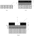
- FIG. 1 showing a flowchart representing a method according to an embodiment of the present disclosure, to be read in combination with Fig. 2 showing a schematic representation of the corresponding cross sections of the substrate after process steps, in order, as used in the embodiments of the present disclosure.
- the method (600) starts with obtaining (25) a substrate (10) to be patterned ( Fig. 2a ).
- the substrate (10) has an upper main surface (5).
- the upper main surface (5) may be in contact with surrounding ambient.
- the substrate may include any underlying material or materials that may be used, or upon which a device may be formed.
- the substrate may be a semiconductor substrate suitable for manufacturing semiconductor devices.
- the semiconductor substrate may be a bulk semiconductor substrate, such as for example, Si, Ge, gallium arsenide (GaAs), a gallium arsenide phosphide (GaAsP), an indium phosphide (InP) or a silicon germanium (SiGe) substrate.
- GaAs gallium arsenide
- GaAsP gallium arsenide phosphide
- InP indium phosphide
- SiGe silicon germanium
- the substrate may comprise different semiconductor layers stacked on top of one another, such as for example silicon germanium (SiGe) vs. germanium (Ge) or silicon (Si) vs. silicon germanium (SiGe).
- SiGe silicon germanium
- SiGe silicon germanium
- SiGe silicon germanium
- the substrate may include for example an insulating layer such as a SiO 2 or a Si 3 N 4 layer in addition to a semiconductor substrate portion.
- the substrate may also be silicon-on-glass, silicon-on sapphire, silicon-on-insulator (SOI) substrate or germanium-on-insulator (GeOI) substrate.
- the substrate may have a main surface of monocrystalline silicon layer.
- fin structures may be patterned in the substrate (10).
- An EUV photoresist layer (40) is provided (200) on the upper main surface (5) by methods known to persons skilled in the art. At least one opening (50) is formed (300) in the EUV photoresist layer (40), thereby forming a patterned EUV photoresist layer (45) ( Fig. 2c ). Formation of the at least one opening (50) is done by the methods known to persons skilled in the art.
- the EUV photolithographic processing may be done at a wavelength in the range of 6 nm to 27 nm. It is advantageous to perform EUV processing at a wavelength in this range since it provides a wavelength range capable of presenting options for tackling EUV lithography related problems. For example, different combinations of elemental atoms may be chosen to be used in the multi-layer stack that have potential to provide enhancement of EUV photoresist sensitivity at wavelengths covered in this range.
- a multi-layer stack (100) is provided (150) sandwiched between and in contact with the EUV photoresist layer (40) and the upper main surface (5) of the substrate (10) ( Fig. 1 and Fig. 2b ).
- the multi-layer stack (100) has an upper surface.
- the at least one opening (50) extends from a top surface (6) of the EUV photoresist layer (40) down to the upper surface of the multi-layer stack (100), thereby exposing a part (7) of the upper main surface of the multi-layer stack ( Fig. 2c ).
- the multi-layer stack (100) consist of a first layer (20) of a first material and a second layer (30) of a second material and the first material and the second material may have different refractive indexes.
- the first layer (20) and the second layer (30) are stacked alternately and repeatedly on one another ( Fig. 2b ).
- Providing the multi-layer stack comprises depositing the first layer (20) and the second layer (30) alternately and repeatedly on one another.
- Chemical vapour deposition (CVD), physical vapour deposition (PVD), spin coating, atomic layer deposition (ALD) or molecular layer deposition (MLD) may be used for the deposition of the first layer (20) and/or the second layer (30) .
- a combination of the first layer (20) and the second layer (30) is called a pair.
- Increasing the numbers of such pairs, thus stacking the first layer (20) and the second layer (30) repeatedly is advantageous since it increases reflectivity due to the reflections occurring at each interface between the first layer (20) and the second layer (30).
- Increasing the refractive index contrast thus stacking the first layer (20) and the second layer (30), which have different refractive indexes, alternatingly leads to an increase both in reflectivity and bandwidth. It is thus advantageous to have the first material and the second material having different refractive indexes. It is thus further advantageous to have as a difference as large as possible in the refractive index of the first material and the second material.
- the difference in the refractive index of the first layer and the second layer may be between 1 % and 15 %. It is advantageous that the refractive indexes of the layers are as far apart as possible from each other in order so that enough contrast exists in between the refractive indexes and so as to enhance the EUV photoresist sensitivity.
- the amount of reflected EUV light, thus the peak reflectance value, entering back into the EUV photoresist layer (40) depends upon the ratio of the refractive index of the first layer (20) and the second layer (30), as well as the number of layer pairs. Thus, the peak reflectance may be increased by adding more layers or by using layers of materials with a higher refractive index ratio.
- optical path length is equal to quarter wavelength of the incident light.
- reflectance is a maximum at the wavelength for which both the high refractive index and the low refractive index layers of the multi-layer stack are exactly one quarter wave thick.
- Optical path length difference ( ⁇ ) in a layer of the multi-layer stack is determined by the product of the geometric path of the light and the index of refraction (n) of the medium through which it propagates.
- the thickness of the layer is also an important factor. Therefore, multi-layer stacks having layers whose product of refractive index and thickness is equal to half the wavelength of EUV wavelength is advantageous in embodiments of the present disclosure.
- the first layer (20) or the second layer (30) of the multi-layer stack (100) may be present in contact with the EUV photoresist layer (40).
- the layer that has the higher refractive index may be in contact with the EUV photoresist layer (40). It is advantageous that the layer of the multi-layer stack having a higher refractive index is in direct contact with the EUV photoresist layer (40) since this allows for more reflections to be created at the interfaces of the first layer (20) and the second layer (30) of the multi-layer stack. More reflections that are coupled constructively leads to improvement of EUV photoresist sensitivity.
- the layer that has the lower refractive index may be in contact with the EUV photoresist layer (40).
- use of more number of pairs in the multi-layer stack (100) or adapting the thickness of each of the layers is the multi-layer stack may allow for creating more reflections at the interfaces of the first layer (20) and the second layer (30) of the multi-layer stack (100).
- the first material and the second material of the multi-layer stack may be elemental materials or compounds.
- the first material and/or the second material of the multi-layer stack may be a metal, a semiconductor, a transition metal or a lanthanide.
- Fig. 3 shows prior art optical properties (refractive index, n)of the first 82 elemental atoms at 13.5 nm wavelength. 13.5 nm is the wavelength currently used for EUV lithographic processing in semiconductor manufacturing.
- Figure 3 permits to identify pairs that are suitable for making the multi-layer stack as disclosed in this disclosure for use in EUV lithographic processing of semiconductor manufacturing carried out in a cleanroom environment.
- the figure presents wide range of elemental atoms that can be combined as a pair and it is advantageous to choose combinations wherein the difference in the refractive index of the first layer and the second layer may be between 1 % and 15 %.
- each elemental atom in such a pair satisfying this condition has extinction coefficients lower than 0.04, preferably lower than 0.02, and yet preferably lower than 0.01.
- Fig. 4 shows, for an embodiment, a PROLITH simulation of the relation between the number of MoSi pairs in a multi-layer stack and the number of photons absorbed by an EUV photoresist layer.
- the simulation region has been taken to be 80x80x40 nm 3 . It is observed that as the number of MoSi pairs increases, the number of absorbed photons increases in the EUV photoresist layer. There exits about 25 % increase in photon absorption when, for example, 20 MoSi pairs are used as a multi-layer stack in comparison to the case when no multi-layer stack consisting of MoSi pairs were used.
- a high reflectance may not be necessary. It may be sufficient to obtain enhancement in reflectance such that a reduction of 10-30 % could be obtained in the dose at the scanner level. From photon absorption point of view, at least 10% increase in absorption in the EUV photoresist layer may be targeted Therefore, fewer number of pairs may be sufficient and the material selection of the first layer (20) and the second layer (30) need not be Mo/Si or limited thereof. The material selection may depend on the trade-off between how easy vs. how cheap it would be to form the multi-layer stack. Besides, the easiness in etching of the multi-layer stack should also be considered. This consideration is important if the multi-layer stack will be used as a hard mask layer.
- the multi-layer stack (100) may be a self-organized di-block copolymer.
- the first material of the first layer of the self-organized di-block copolymer may be a first polymer component containing silicon or silicon and a metal.
- the second material of the second layer of the self-organized di-block copolymer may be a second polymer component.
- the multi-layer stack (100) may be a self-organized di-block copolymer.
- the first material of the first layer of the self-organized di-block copolymer may be a first polymer component containing silicon and the second material of the second layer of the self-organized di-block copolymer may be a second polymer component containing a metal.
- the metal in these embodiments, may for example, be Mo.
- the self-organized di-block copolymer having the first polymer component containing silicon and having the second component containing Mo may possess the desired reflective properties for EUV photoresist sensitivity enhancement.
- the self-organized di-block copolymer may be PS-b-PMMA, where silicon may be contained in PMMA, since typically, PMMA is easy to modify.
- the first polymer component contains silicon or silicon and the metal, since in this way refractive index of the domains originating from the first polymer component will be higher than the refractive index of the domains originating from the second polymer component, which contain mostly carbon atoms.
- the first material of the first layer of the self-organized di-block copolymer may be a first polymer component containing a metal or a metal oxide.
- the second material of the second layer of the self-organized di-block copolymer may be a second polymer component.
- the metal oxide may be a ceramic material.
- the ceramic material may be any ceramic material that may be grown by Atomic layer Deposition (ALD) technique such as for example but not limited to, aluminum oxide, titanium oxide, hafnium oxide, zirconium oxide, zinc oxide, or silicon oxide.
- ALD Atomic layer Deposition
- the self-organized di-block copolymer may be PS-b-PMMA, where metal may be contained in PMMA, since typically, PMMA is easy to modify.
- the self-organized di-block copolymer may be PS-b-PMMA, where metal oxide may be contained in PMMA, since typically, PMMA is easy to modify.
- the first polymer component contains the metal or the metal oxide since in this way refractive index of the domains originating from the first polymer component will be higher than the refractive index of the domains originating from the second polymer component, which contain mostly carbon atoms.
- self-organized di-block copolymer having the first polymer component, which has silicon, silicon and metal, or ceramic material and the second polymer component will be aligned alternatingly and repeatedly. This will create the multi-layer stack of layer of materials having different refractive indexes, thereby helping to enhance EUV photoresist sensitivity due to more reflections of EUV light at each interface between the material layers.
- the multi-layer stack of the self-organized di-block copolymer having the first polymer component containing a metal or a ceramic material and the second polymer component may be provided by depositing a self-organized di-block copolymer on the main surface of the substrate (10).
- the self-organized di-block copolymer may consist of the first polymer component and the second polymer component. Micro phase separation takes place as a result of a thermal annealing process, thus forming the domains.
- SIS sequential infiltration synthesis
- the metal oxide may be a ceramic material, such as for example, Al203.
- the ceramic material may also be any ceramic material that may be grown by Atomic layer Deposition (ALD) technique such as for example, aluminum oxide, titanium oxide, hafnium oxide, zirconium oxide, zinc oxide, or silicon oxide.
- ALD Atomic layer Deposition
- the orientation of the di-block copolymer domains with respect to the substrate is crucial for the application disclosed in the present disclosure. Therefore, in embodiments, lamella lying parallel to the main surface of the substrate (10) may be preferred.
- the di-block copolymer may be designed such that lamella lying parallel to the main surface of the substrate (10) may be obtained.
- the surface effects become less dominant away from the main surface of the substrate and thus, a parallel orientation can only be achieved throughout the film if the film is thin enough.
- the di-block copolymer has preferential wetting with respect to both the main surface of the substrate and the free surface (e.g. air)
- one of the polymer components tends to segregate to both surfaces thus, forming a layer of the first polymer component of thickness of dp/4 at each surface.
- the total film thickness is therefore equal to integer of the lamellar period dp of the copolymer.
- the multi-layer stack may be a self-organized high-chi di-block copolymer.
- the first material of the first layer of the self-organized high-chi di-block copolymer may be a first polymer component.
- the second material of the second layer of the self-organized high-chi di-block copolymer may be a second polymer component. It is advantageous to have a self-organized high-chi di-block copolymer since domains of the high-chi di-block copolymer may provide the required refractive index contrast. It is further advantageous to have a self-organized high-chi di-block copolymer since they have a tendency to spontaneously form parallel oriented lamellae due to preferential wetting of both the main surface of the substrate and the free surface, for example air.
- the multi-layer stack may be a self-organized di-block copolymer since the self-organized di-block copolymer can be easily deposited on the substrate (10) without requiring multiple deposition steps.
- a di-block copolymer may be deposited by spin coating on the substrate (10). After deposition, following a thermal annealing process, the spin-coated di-block copolymer phase separates, thereby forming domains of the first polymer component and the second polymer component.
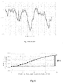
- FIG. 5 shows aerial image of the light intensity in the EUV photoresist layer.
- a refractive index of 1.01 may, for example, correspond to that of silicon or aluminum or a Spin-On Glass, while a refractive index of 0.97 may, for example, correspond to that of a PMMA domain of a di-block copolymer, or a Spin-On Carbon.
- this example may, for example, represent a self-organized di-block copolymer, wherein the first material of the first layer is a first polymer component containing a metal such as Aluminum and the second material of the second layer is a second polymer component, which is PMMA according to one of the embodiments of the present disclosure.
- This example may further represent a multi-layer stack, wherein the first material of the first layer may be a Spin-on-Glass (SOG) and the second material of the second layer may be a Spin-on-Carbon (SOC).
- SOG Spin-on-Glass
- SOC Spin-on-Carbon
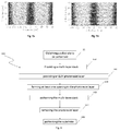
- FIG. 6 showing a flowchart representing a method according to an embodiment of the present disclosure in combination with Fig. 7 showing a schematic representation of the corresponding cross sections of the substrate after process steps, in order, as used in the embodiments of the present disclosure.
- the steps (400), (500) and (600) of the method (610) illustrated in Fig. 6 may be performed subsequent to the step (300) of the method (600) illustrated in Fig. 1 .
- the method (610) may further comprise patterning(400) the multi-layer stack (100) by etching through the at least one opening (50) in the EUV photoresist layer, thereby forming a patterned multi-layer stack (105) having an opening (55).
- the opening (55) exposes at its bottom a part (5') of the main surface (5) of the substrate (10).
- the etching of the multi-layer stack may be performed as known to persons skilled in the art.
- the method (610) further comprises removing the photoresist layer (45) ( Fig. 7b ), thereby obtaining the patterned multi-layer stack (105) on the substrate (10).
- the patterned multi-layers stack (105) may be used as a hard mask layer for further patterning of the substrate (10).
- the substrate (10) is patterned by performing an etch process and etching the substrate through the opening (60) in the patterned multi-layer stack (105) ( Fig. 7c ), thereby forming an opening (65).
- the multi-layer stack may be removed after completing the etching process, thereby forming a patterned substrate (15) having at least an opening (70) ( Fig. 7d ).
- the choice of the layers of the multi-layers stack is, thus, important such that etching characteristics should be considered so that the multi-layer stack has properties suitable for a hard mask and thus can be used as a hard mask.
- the multi-layers stack as a hard mask since this may help to eliminate the problem of EUV photoresist layer consumption.
- EUV photoresist layer consumption As industry is moving to the implementation of EUV lithographic processing due to shrinkage in feature sizes, photoresist thicknesses are being reduced. This in turn results in additional challenges such as the consumption of the EUV photoresist layer especially when patterning high aspect ratio features in the substrate.
- a multi-layer stack as disclosed in the present disclosure, not only EUV photoresist sensitivity is enhanced but at the same time EUV photoresist consumption does not pose a challenge anymore since patterning of the substrate will be facilitated by the presence of the patterned multi-layer stack, which may be used as a hard mask.
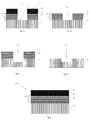
- the intermediate structure (800) comprises a substrate (10) having an upper main surface.
- a multi-layer stack (100) is present directly on and in contact with the upper main surface.
- the multilayer stack (100) consists of a first layer (20) of a first material and a second layer (30) of a second material. The materials have different refractive indexes, and the layers (20, 30) are stacked alternately and repeatedly on one another.
- the multi-layer stack (100) further comprises an EUV photoresist layer (40) directly on and in contact with the multi-layer stack (100).
- the multi-layer stack is, thus, situated sandwiched in between and in contact with the EUV photoresist layer (40) and the upper main surface of the substrate (10).
- the refractive index of the first material may be higher than that of the second material, and the first layer (20) of this first material of the multi-layer stack may be in direct contact with the EUV photoresist layer (40).
- the refractive index of the first material may be higher than that of the second material, however, the second layer (30) of the second material of the multi-layer stack may be in direct contact with the EUV photoresist layer (40). This is also advantageous. Even though there will be little reflectance generated at the interface between the EUV photoresist layer and the second layer of the multi-layer stack, there will be enough reflectance created at all other subsequent interfaces to provide the enhanced EUV photoresist sensitivity.
- the EUV photoresist layer (40) may have a thickness suitable for EUV lithographic processing.
- the difference between the refractive index of the first layer and the second layer may be between 1 % and 15 %. It is advantageous that the refractive indexes of the layers are as far apart as possible from each other in order so that enough contrast exists in between the refractive indexes and so as to enhance the EUV photoresist sensitivity. Although a weak EUV photoresist sensitivity maybe experienced with layers having a refractive index difference of 1 %, it still presents to be advantageous in comparison to cases where no multi-layer stack is used.
- the first material of the first layer (20) and/or the second material of the second layer (30) of the multi-layer stack (100) may be a metal, a semiconductor, a transition metal or a lanthanide. It is advantageous that metals, semiconductors, transition metals or lanthanides offer combinations to be used as a multi-layer stack that can enhance EUV photoresist sensitivity. Within these classes of materials offering combinations to be used as a multi-layer stack, it is advantageous, in embodiments of the disclosure, that candidate materials to be used as the first layer (20) and the second layer (30) may have refractive indexes in the range of 0.85 and 1.05 at 13.5 nm wavelength since EUV lithography is currently performed at 13.5 nm in semiconductor manufacturing.
- the materials possess low values of extinction coefficients may be lower than 0.08, preferably lower than 0.06. In embodiments, the extinction coefficient may yet preferably be lower than 0.04 and even more preferably lower than 0.02.
- the first material of the first layer (20) and the second material of the second layer (30) may be an organic polymer.
- the organic polymer of the first layer (20) and/or the second layer (30) may be doped with a dopant element.
- the dopant element may be chosen from among the ones presented in Fig. 3 .
- the dopant type and/or the dopant concentration may be adjusted such that a refractive index difference in the range of 1 % to 15 % exists between the first layer (20) and the second layer (30).
- the multi-layer stack (100) may be a self-organized di-block copolymer.
- the first material of the first layer of the self-organized di-block copolymer may be a first polymer component containing silicon or silicon and a metal while the second material of the second layer may be a second polymer component. Having the first polymer component containing silicon or silicon and a metal will increase the refractive index compared to the second polymer component. This will allow for enhancing reflections of the EUV light from each of the interfaces between the first layer and the second layer.
- the first polymer component containing silicon or silicon and a metal may be the layer of the multi-layer stack that is in direct contact with the EUV photoresist layer (40).
- the multi-layer stack may be a self-organized di-block copolymer.
- the first material of the first layer may be a first polymer component containing a metal or a metal oxide and the second material of the second layer may be a second polymer component.
- the first polymer component containing a metal or metal oxide may be the layer of the multi-layer stack (100) that is in direct contact with the EUV photoresist layer (40).
- the multi-layer stack may be a self-organized high-chi di-block copolymer.
- the first material of the first layer of the self-organized high-chi di-block copolymer may be a first polymer component.
- the second material of the second layer of the self-organized high-chi di-block copolymer may be a second polymer component.
- the first layer (20) and the second layer (30) of the multi-layer stack (100) make up a pair and the total thickness of the multi-layer stack depends on the total number of these pairs.
- the relative thicknesses of the first layer (20) and the second layer (30) in the multi-layer stack (100) are also critical for having an optimized reflectivity.
- optical path length difference is equal to quarter wavelength of the incident light, which is also equal to the product of the geometric path length of the refracted light and the refractive index of the medium in which it travels. Reflectance is a maximum at the wavelength for which both the high refractive index and the low refractive index layers of the multi-layer stack are exactly one quarter wave thick.
- the peak reflectance that would be observed in the EUV photoresist layer (40) may be increased by adding more layers or more number of pairs or by using layers of materials with a higher refractive index ratio.
Landscapes
- Physics & Mathematics (AREA)
- General Physics & Mathematics (AREA)
- Engineering & Computer Science (AREA)
- Architecture (AREA)
- Structural Engineering (AREA)
- Exposure And Positioning Against Photoresist Photosensitive Materials (AREA)
- Photosensitive Polymer And Photoresist Processing (AREA)
- Exposure Of Semiconductors, Excluding Electron Or Ion Beam Exposure (AREA)
Abstract
Description
- The present disclosure is related to the field of extreme ultraviolet lithography (EUVL). More specifically, the present disclosure relates to a method and a structure for performing EUVL with increased resist sensitivity.
- Extreme Ultraviolet Lithography (EUVL) is targeted to be choice of lithographic patterning technique in the manufacture of ultra large scale integration systems (ULSI) in semiconductor industry, which manufacturing is driven by the motivation of keeping up with Moore's Law. Due to feature size shrinkage following this motivation, photoresist films must be made thinner to keep a reasonable aspect ratio and avoid pattern collapse. However, due to the small thickness of EUV resist, which may typically be in the range of 10 nm to 60 nm, only a small portion, typically about 10-30%, of the EUV radiation that impinges on the wafer is absorbed by the photoresist layer. The remainder of the light passes through the photoresist layer and is absorbed in the substrate. This raises an issue for the performance of the EUV Lithography and presents itself as a challenge to be overcome for a successful integration of EUVL. In this respect, enhancement of EUV photoresist sensitivity becomes an important criteria in order to improve the performance of the EUV lithography.
- Underlayer materials applied under the EUV photoresist have been proposed for the purpose of promoting adhesion as well as reducing pattern collapse. Furthermore, underlayer materials are used to enhance EUV photosensitivity of resist, however none of these layers has been shown to work experimentally so far. The use of an underlayer mainly relies on redirecting the energy from the EUV photons back to the EUV photoresist in the form of photons, secondary electrons or photo-acid-generators (PAGs) has been referred to in the work of H. Xu et.al. Proceedings of SPIE V. 7273, 2009 . The work J.S. Kim et. al, J. Vac. Sci. Technol. B (33)6, 2015 presents simulation results with respect to the use of an underlayer with lower refractive indexes under the photoresist layer leading to increased reflection at the photoresist/underlayer interface that resulted in an increased number of photons in the photoresist layer. They conclude that the difference in refractive index between the underlayer and the photoresist should be maintained below 5% in order to optimize photoresist imaging performance for both the dense and isolated patterns.
- The likelihood of success with redirecting the energy from the EUV photons back to the EUV photoresist in the form of secondary electrons is questionable since the thermalization distance of these electrons, which is typically 1nm to 3nm, is very short compared to the photoresist film thickness, which is typically in the range of 10 nm to 60nm.
- While the use of PAGs, on the other hand, can result in keeping the photoresist profile straight by reducing footing and scumming, uncontrolled photo-acid diffusion can still result in RLS trade-off by compromising LER and resolution as disclosed in the work of H. Xu et. al., Proc. Of SPIE Vol. 7273, 2009.
- Therefore, there is still a need in the art for methods and structures that can improve EUV lithography performance and can provide EUV photoresist sensitivity enhancement without jeopardizing lithographic performance indicators such as, for example, line edge roughness (LER), line width roughness (LWR) and resolution and without imposing limitative remedies.
- It is an object of the present disclosure to provide methods and structures for increasing the performance of the EUV lithography.
- It is an object of the present disclosure to provide methods and structures for performing EUV lithographic processing with increased photon absorption in the EUV photoresist layer, thereby increasing EUV photoresist layer sensitivity.
- It is an object of the present disclosure to provide methods and structures for performing EUV lithographic processing, whereby EUV photoresist layer sensitivity is enhanced.
- It is an advantage of the embodiments of the present disclosure that an enhancement in EUV photoresist sensitivity may be provided by using a multi-layer stack since reflected EUV photons will go back into the EUV photoresist layer, thus increasing photon absorption in the EUV photoresist layer.
- It is, therefore, an advantage of the embodiments of the present disclosure that enhancement in EUV photoresist sensitivity leads to reduce the dose applied at the scanner level, compared to state of the art, during the EUV lithographic processing.
- It is an advantage of the embodiments of the present disclosure that reduction of dose at the scanner level, in turn, increases the throughput of the EUV lithographic processing.
- It is an advantage of the embodiments of the present disclosure that line width roughness (LWR)of patterned structures in the underlying substrate may be reduced.
- It is an advantage of the embodiments of the present disclosure that the multi-layer stack may be a Bragg reflector.
- It is an advantage of the embodiments of the present disclosure that the multi-layer stack is suitable for use as an etch mask to pattern the underlying substrate. In this way, the multi-layer stack may act as a hard mask layer as well as a layer for enhancing EUV photoresist sensitivity.
- The above objective is accomplished by a method and an intermediate structure according to the present disclosure.
- In a first aspect, the present disclosure relates to a method for performing an extreme ultraviolet (EUV) lithographic processing. The method comprises obtaining a substrate to be patterned. This substrate has an upper main surface. An EUV photoresist layer is provided on the upper main surface and at least one opening is formed in the EUV photoresist layer. The method further comprises providing a multi-layer stack that is sandwiched between the EUV photoresist layer and the upper main surface of the substrate. The multi-layer stack has an upper surface and consists of a first layer of a first material and a second layer of a second material. The first material and the second material have different refractive indexes and the first layer and the second layer are stacked alternatingly and repeatedly on one another. The at least one opening exposes a part of the upper main surface of the multilayer stack.
- The disclosure originates from the realization by the inventors that the presence of a multi-layer stack, which is present in contact with and in between the EUV photoresist layer and the substrate, leads to the occurrence of more reflections of EUV light from each of the interfaces between the layers of the multi-layer stack that enter back into the EUV photoresist layer.
- The present disclosure takes advantage of redirecting the EUV photons back to the EUV photoresist layer in order to enhance EUV photoresist sensitivity. In this way, the dose at the scanner level may also be reduced since the dose felt by the EUV photoresist layer will be higher than the dose set at the scanner level thanks to the presence of the multi-layer stack under the EUV photoresist layer.
- Reducing the dose at the scanner level is advantageous because it will lead to an increase in the throughput, where currently low throughput is one of the major drawbacks of the EUV photolithographic processing. Since the absorbed photons in the EUV photoresist layer will be higher, the photon shot noise in the EUV photoresist layer will be reduced for the value of dose set at the scanner level. Consequently, LWR of the features to be patterned in the substrate will be reduced when compared with the features patterned at the identical value of dose set at the scanner in the absence of a multi-layer stack. Typically, when the absorption point of each photon is mapped individually, a noise is obtained compared to a continuous aerial image of light absorption. The more photons there would be, the closer the particle representation will be to the aerial representation. Therefore, it is for this reason that increased photon absorption would reduce photon shot noise. Due to the fact that this photon shot noise is partially responsible for LWR, reducing this noise would imply reduction of the LWR.
- Enhancement of EUV photoresist sensitivity by sending back EUV photons achieved according to embodiments of the present disclosure is advantageous in comparison to sending secondary electrons back to the EUV photoresist layer by using an underlayer. This is due to the fact that only about 5 nm at the bottom of the EUV photoresist layer would take advantage of sensitivity enhancement. Typically, for positive-tone developer photoresists, this short ranged benefit is due to the short thermalization distance of the secondary electrons and this would then likely pose a risk of dissolution at the interface, thereby leading to pattern collapse. On the other hand, for negative-tone developer photoresists, a potential risk is to have large footing at the bottom of the photoresist features. Thus, whether a positive-tone or a negative-tone developer photoresist is used, profile of the photoresist is impacted in either of the cases. Present disclosure is further advantageous in comparison to the use of photo-acid generators due to the fact that it can lead to problems or challenges with respect to LER and/or resolution of patterned features in the substrate.
- In embodiments, the refractive index of the first material may be higher than that of the second material and the first layer of the first material of the multi-layer stack may be in direct contact with the EUV photoresist layer. It is advantageous that the layer of the material having higher refractive index is in contact with the EUV photoresist layer since it leads to the formation of higher amount of reflections from successive layers, thus having a higher chance of enhancing EUV sensitivity.
- In embodiments, the refractive index of the first material may be lower than that of the second material, and the first layer of the first material of the multi-layer stack may be in direct contact with the EUV photoresist layer.
- In embodiments, the EUV photolithographic processing is done at a wavelength in the range of 6 nm to 27 nm. It is advantageous to perform EUV processing at a wavelength in this range since it provides a broad wavelength range that may present more options for tackling EUV lithography related problems.
- In embodiments, the difference in the refractive index of the first layer and the second layer is between 1 % and 15 %. It is advantageous that the refractive indexes of the layers are as far apart as possible from each other so that enough contrast exists in between the refractive indexes and so as to enhance the EUV photoresist sensitivity.
- In embodiments, the multi-layer stack may be a self-organized di-block copolymer. It is advantageous to use the di-block copolymer as the multi-layer stack since it does not require repetitive deposition steps of the first layer and the second layer. The first material of the first layer of the self-organized di-block copolymer may be a first polymer component containing silicon or silicon and a metal while the second material of the second layer may be a second polymer component. Having the first polymer component containing silicon or silicon and a metal will increase the refractive index compared to the second polymer component. This will allow for enhancing reflections of the EUV light from each of the interfaces between the first layer and the second layer.
- In embodiments, the multi-layer stack may be a self-organized di-block copolymer. The first material of the first layer may be a first polymer component containing a metal or a metal oxide and the second material of the second layer may be a second polymer component. It is advantageous to use the di-block copolymer as the multi-layer stack since it does not require repetitive deposition steps of the first layer and the second layer. Furthermore, it requires an easy process to provide the self-organized di-block copolymer, where the first material of the first layer may be a first polymer component containing a metal or a metal oxide.
- In embodiments, the metal oxide may be a ceramic material. In embodiments, the ceramic material may be any material that may be grown by Atomic layer Deposition (ALD) technique such as for example, aluminum oxide, titanium oxide, hafnium oxide, zirconium oxide, zinc oxide, or silicon oxide.
- In embodiments, the multilayer stack may be a self-organized high-chi di-block copolymer. The first material of the first layer may be a first polymer component and the second material of the second layer may be a second polymer component.
- In embodiments, providing the self-organized di-block copolymer as the multi-layer stack wherein the first material of the first layer may be a first polymer component containing a metal or a ceramic material comprises depositing a self-organizing di-block copolymer consisting of the first polymer component and the second polymer component, phase separating the self-organizing di-block copolymer and infusing the first polymer component with the metal or the metal oxide. Infusing the first polymer component with metal or metal oxide helps to create sufficient difference in the real part "n" of the refractive indexes such that EUV photosensitivity can be obtained.
- In preferred embodiments, the metal may be aluminum.
- In preferred embodiments, the metal oxide may be aluminum oxide.
- In embodiments, the first material of the first layer and/or the second material of the second layer may be a metal, a semiconductor, a transition metal or a lanthanide. It is advantageous that metals, semiconductors, transition metals or lanthanides offer combinations to be used as a multi-layer stack that can enhance EUV photoresist sensitivity.
- In embodiments, the first material of the first layer and the second material of the second layer may have the their refractive indexes in the range from 0.85 to 1.05 at 13.5 nm wavelength.
- In embodiments, the method may further comprise patterning the multi-layer stack by etching through the at least one opening in the EUV photoresist layer. After removing the EUV photoresist layer, the substrate may be patterned using the patterned multi-layer stack as a hard mask. It is advantageous that the multi-layer stack may also be used as the hard mask since this simplifies the process flow such that the need for having extra hard mask layer is moot.
- In a second aspect, the present disclosure relates to an intermediate structure. The intermediate structure comprises a substrate having an upper main surface and a multi-layer stack on the main surface. The multi-layer stack consists of a first layer of a first material and a second layer of a second material. The materials have a different refractive indexes and the layers are stacked alternately and repeatedly in one another. The intermediate structure further comprises an EUV photoresist layer, where the multi-layer stack is in contact and is sandwiched between the EUV photoresist layer and the upper main surface of the substrate.
- In embodiments, the refractive index of the first material may be higher than that of the second material, and the first layer of the first material of the multi-layer stack may be in direct contact with the EUV photoresist layer. It is advantageous to have the layer of the material having higher refractive index in contact with the EUV photoresist layer, since it leads to the formation of higher amount of reflections from successive layers, thus having an EUV photoresist layer with enhanced EUV sensitivity.
- In embodiments, the refractive index of the first material may be lower than that of the second material, and the first layer of the first material of the multi-layer stack may be in direct contact with the EUV photoresist layer.
- In embodiments, the difference in the refractive index of the first layer and the second layer may be between 1 % and 15 %. It is advantageous that the refractive indexes of the layers are as far apart as possible from each other so that enough contrast exists in between the refractive indexes and so as to enhance the EUV photoresist sensitivity.
- In embodiments, the first layer and the second layer may have the refractive indexes in the range of 0.85 and 1.05 at 13.5 nm wavelength.
- Particular and preferred aspects of the disclosure are set out in the accompanying independent and dependent claims. Features from the dependent claims may be combined with features of the independent claims and with features of other dependent claims as appropriate and not merely as explicitly set out in the claims.
- Although there has been constant improvement, change and evolution of devices and methods in this field, the present concepts are believed to represent substantial new and novel improvements, including departures from prior practices, resulting in the provision of more efficient, stable and reliable devices or methods of this nature.
- The above and other characteristics, features and advantages of the present disclosure will become apparent from the following detailed description, taken in conjunction with the accompanying drawings, which illustrate, by way of example, the principles of the disclosure. This description is given for the sake of example only, without limiting the scope of the disclosure. The reference figures quoted below refer to the attached drawings.
-
-
Fig. 1 is a flowchart representing a method according to an embodiment of the present disclosure. -
Fig. 2a to Fig. 2c show a schematic representation of process steps, in order, as used in the embodiments of the present disclosure. -
Fig. 3 shows prior art optical properties refraction index, n) of the first 82 elemental atoms at 13.5 nm wavelength. -
Fig. 4 shows PROLITH simulation of the relation between the number of MoSi pair in a multi-layer stack used as underlayer and the number of photon absorbed by an EUV photoresist layer according to an embodiment. -
Fig. 5 shows aerial image of the light intensity in the EUV photoresist layer: (a) resist on a traditional substrate, (b) resist with a multi-layer stack composed of 20 layers of material with n1 =1.01 and n2 = 0.97 according to an embodiment. -
Fig. 6 is a flowchart representing a method according to an embodiment of the present disclosure. -
Fig 7a to Fig. 7d shows a schematic representation of process steps, in order, as used in further embodiments of the present disclosure. -
Fig. 8 shows an intermediate structure obtained according to the embodiments of the present disclosure. - The figures are only schematic and are non-limiting. In the drawings, the size of some of the elements may be exaggerated and not drawn on scale for illustrative purposes. Any reference signs in the claims shall not be construed as limiting the scope. In the different drawings, the same reference signs refer to the same or analogous elements.
-
Fig. 2 andFig. 7 show corresponding cross-sections of the substrate at different stages of the method. Purely to facilitate understanding, different layers are shown with different filling patterns. This should not be construed in any limiting sense. - The present disclosure will be described with respect to particular embodiments and with reference to certain drawings but the disclosure is not limited thereto but only by the claims. The drawings described are only schematic and are non-limiting. In the drawings, the size of some of the elements may be exaggerated and not drawn on scale for illustrative purposes. The dimensions and the relative dimensions do not correspond to actual reductions to practice of the disclosure.
- It is to be noticed that the term "comprising", used in the claims, should not be interpreted as being restricted to the means listed thereafter; it does not exclude other elements or steps. It is thus to be interpreted as specifying the presence of the stated features, integers, steps or components as referred to, but does not preclude the presence or addition of one or more other features, integers, steps or components, or groups thereof.
- Reference throughout the specification to "one embodiment" or "an embodiment" means that a particular feature, structure or characteristic described in connection with the embodiment is included in at least one embodiment of the present disclosure. Thus, appearances of the phrases "in one embodiment" or "in an embodiment" in various places throughout the specification are not necessarily all referring to the same embodiment, but may. Furthermore, the particular features, structures or characteristics may be combined in any suitable manner, as would be apparent to one of ordinary skill in the art from the disclosure, in one or more embodiments.
- Similarly it should be appreciated that in the description of exemplary embodiments of the disclosure, various features of the disclosure are sometimes grouped together in a single embodiment, figure, or description thereof for the purpose of streamlining the disclosure and aiding in the understanding of one or more of the various inventive aspects. The method of disclosure, however, is not to be interpreted as reflecting an intention that the claimed disclosure requires more features than are expressly recited in each claim. Rather, as the following claims reflect, inventive aspects lie in less than all features of a single foregoing disclosed embodiment. Thus, the claims following the detailed description are hereby expressly incorporated into the detailed description, with each claim standing on its own as a separate embodiment of the disclosure.
- Furthermore, while some embodiments described herein include some but not other features included in other embodiments, combinations of features of different embodiments are meant to be within the scope of the disclosure, and form different embodiments, as would be understood by those in the art. For example, in the following claims, any of the claimed embodiments can be used in any combination.
- In the description provided herein, numerous specific details are set forth. However, it is understood that embodiments of the disclosure may be practiced without these specific details. In other instances, well-known methods, structures and techniques have not been shown in detail in order not to obscure an understanding of the description.
- The following terms are provided solely to aid in the understanding of the disclosure.
- As used herein and unless provided otherwise, refractive index refers to the real part "n" of the complex refractive index.
- As used herein and unless provided otherwise, path length difference refers to the optical path length difference, which is determined by the product of the geometric path length of the light and the index of refraction of the medium through which it propagates. Geometric path length is a function of the thickness of the layer through which the refracted light passes. Thus, in case of normal incidence, for example when light is directed normal to the surface of the layer, geometrical path length is approximately equal to twice the film thickness, 2(t) since refracted light passes through the film thickness (t) twice.
- As used herein and unless provided otherwise, a di-block copolymer refers to a block copolymer having two different homo polymers A and B that are linked via a covalent bond.
- As used herein and unless provided otherwise, a high-chi block copolymer refers to a di-block copolymer having a high value of Flory-Huggins interaction parameter.
- As used herein and unless provided otherwise, lamella refers to ordered micro-phase structures that are formed during the micro-phase separation of the block copolymer.
- As used herein and unless provided otherwise, thermalization distance refers to the distance between a secondary electron and its originating cation where it has lost enough energy and is at equilibrium.
- As used herein and unless provided otherwise, footing refers to the non-straight profile of any feature, where the width at the bottom region of the feature is wider than the width at the upper region.
- As used herein and unless provided otherwise, throughput refers to productivity of a process expressed over a unit period.
- The disclosure will now be described by a detailed description of several embodiments of the disclosure. It is clear that other embodiments of the disclosure can be configured according to the knowledge of persons skilled in the art without departing from the technical teaching of the disclosure, the disclosure being limited only by the terms of the appended claims.
- We now refer to
Fig. 1 showing a flowchart representing a method according to an embodiment of the present disclosure, to be read in combination withFig. 2 showing a schematic representation of the corresponding cross sections of the substrate after process steps, in order, as used in the embodiments of the present disclosure. - The method (600) starts with obtaining (25) a substrate (10) to be patterned (
Fig. 2a ). The substrate (10) has an upper main surface (5). The upper main surface (5) may be in contact with surrounding ambient. - In embodiments, the substrate may include any underlying material or materials that may be used, or upon which a device may be formed.
- In embodiments, the substrate may be a semiconductor substrate suitable for manufacturing semiconductor devices. The semiconductor substrate may be a bulk semiconductor substrate, such as for example, Si, Ge, gallium arsenide (GaAs), a gallium arsenide phosphide (GaAsP), an indium phosphide (InP) or a silicon germanium (SiGe) substrate.
- In embodiments, the substrate may comprise different semiconductor layers stacked on top of one another, such as for example silicon germanium (SiGe) vs. germanium (Ge) or silicon (Si) vs. silicon germanium (SiGe).
- In embodiments, the substrate may include for example an insulating layer such as a SiO2 or a Si3N4 layer in addition to a semiconductor substrate portion. Thus, the substrate may also be silicon-on-glass, silicon-on sapphire, silicon-on-insulator (SOI) substrate or germanium-on-insulator (GeOI) substrate.
- In one particular embodiment, the substrate may have a main surface of monocrystalline silicon layer. In this particular embodiment, fin structures may be patterned in the substrate (10).
- An EUV photoresist layer (40) is provided (200) on the upper main surface (5) by methods known to persons skilled in the art. At least one opening (50) is formed (300) in the EUV photoresist layer (40), thereby forming a patterned EUV photoresist layer (45) (
Fig. 2c ). Formation of the at least one opening (50) is done by the methods known to persons skilled in the art. - In embodiments, the EUV photolithographic processing may be done at a wavelength in the range of 6 nm to 27 nm. It is advantageous to perform EUV processing at a wavelength in this range since it provides a wavelength range capable of presenting options for tackling EUV lithography related problems. For example, different combinations of elemental atoms may be chosen to be used in the multi-layer stack that have potential to provide enhancement of EUV photoresist sensitivity at wavelengths covered in this range.
- A multi-layer stack (100) is provided (150) sandwiched between and in contact with the EUV photoresist layer (40) and the upper main surface (5) of the substrate (10) (
Fig. 1 andFig. 2b ). The multi-layer stack (100) has an upper surface. The at least one opening (50) extends from a top surface (6) of the EUV photoresist layer (40) down to the upper surface of the multi-layer stack (100), thereby exposing a part (7) of the upper main surface of the multi-layer stack (Fig. 2c ). - The multi-layer stack (100) consist of a first layer (20) of a first material and a second layer (30) of a second material and the first material and the second material may have different refractive indexes. The first layer (20) and the second layer (30) are stacked alternately and repeatedly on one another (
Fig. 2b ). - Providing the multi-layer stack comprises depositing the first layer (20) and the second layer (30) alternately and repeatedly on one another. Chemical vapour deposition (CVD), physical vapour deposition (PVD), spin coating, atomic layer deposition (ALD) or molecular layer deposition (MLD) may be used for the deposition of the first layer (20) and/or the second layer (30) .
- A combination of the first layer (20) and the second layer (30) is called a pair. Increasing the numbers of such pairs, thus stacking the first layer (20) and the second layer (30) repeatedly is advantageous since it increases reflectivity due to the reflections occurring at each interface between the first layer (20) and the second layer (30). Increasing the refractive index contrast, thus stacking the first layer (20) and the second layer (30), which have different refractive indexes, alternatingly leads to an increase both in reflectivity and bandwidth. It is thus advantageous to have the first material and the second material having different refractive indexes. It is thus further advantageous to have as a difference as large as possible in the refractive index of the first material and the second material.
- In embodiments, the difference in the refractive index of the first layer and the second layer may be between 1 % and 15 %. It is advantageous that the refractive indexes of the layers are as far apart as possible from each other in order so that enough contrast exists in between the refractive indexes and so as to enhance the EUV photoresist sensitivity.
- Consequently, EUV light reflected at each interface between the first layer (20) and the second layer (30) will enter back into the EUV photoresist layer, thereby enhancing its photosensitivity.
- The amount of reflected EUV light, thus the peak reflectance value, entering back into the EUV photoresist layer (40) depends upon the ratio of the refractive index of the first layer (20) and the second layer (30), as well as the number of layer pairs. Thus, the peak reflectance may be increased by adding more layers or by using layers of materials with a higher refractive index ratio.
- For multi-layer stacks consisting of repeated and alternating layers of high and low refractive index materials, optical path length is equal to quarter wavelength of the incident light. Thus, reflectance is a maximum at the wavelength for which both the high refractive index and the low refractive index layers of the multi-layer stack are exactly one quarter wave thick.
- Optical path length difference (Δ) in a layer of the multi-layer stack is determined by the product of the geometric path of the light and the index of refraction (n) of the medium through which it propagates. For EUV light, having a wavelength λ, arriving at normal incidence to the surface, the optical path length difference is approximately equal to twice the film thickness (t) and the following equation would hold for producing constructive interference :

- Thus, the thickness of the layer is also an important factor. Therefore, multi-layer stacks having layers whose product of refractive index and thickness is equal to half the wavelength of EUV wavelength is advantageous in embodiments of the present disclosure.
- When light passes through a medium, some part of it will always be attenuated such that there will be a gradual loss in intensity of any kind of flux through a medium. This is usually taken into account by defining a complex refractive index expressed as :

- In embodiments, the first layer (20) or the second layer (30) of the multi-layer stack (100) may be present in contact with the EUV photoresist layer (40).
- In embodiments, the layer that has the higher refractive index may be in contact with the EUV photoresist layer (40). It is advantageous that the layer of the multi-layer stack having a higher refractive index is in direct contact with the EUV photoresist layer (40) since this allows for more reflections to be created at the interfaces of the first layer (20) and the second layer (30) of the multi-layer stack. More reflections that are coupled constructively leads to improvement of EUV photoresist sensitivity.
- In embodiments, the layer that has the lower refractive index may be in contact with the EUV photoresist layer (40). In this case, use of more number of pairs in the multi-layer stack (100) or adapting the thickness of each of the layers is the multi-layer stack may allow for creating more reflections at the interfaces of the first layer (20) and the second layer (30) of the multi-layer stack (100).
- In embodiments, the first material and the second material of the multi-layer stack may be elemental materials or compounds.
- In embodiments, the first material and/or the second material of the multi-layer stack may be a metal, a semiconductor, a transition metal or a lanthanide.
-
Fig. 3 shows prior art optical properties (refractive index, n)of the first 82 elemental atoms at 13.5 nm wavelength. 13.5 nm is the wavelength currently used for EUV lithographic processing in semiconductor manufacturing.Figure 3 permits to identify pairs that are suitable for making the multi-layer stack as disclosed in this disclosure for use in EUV lithographic processing of semiconductor manufacturing carried out in a cleanroom environment. The figure presents wide range of elemental atoms that can be combined as a pair and it is advantageous to choose combinations wherein the difference in the refractive index of the first layer and the second layer may be between 1 % and 15 %. It is advantageous that the refractive indexes of the layers are as far apart as possible from each other in order so that enough contrast exists in between the refractive indexes and so as to enhance the EUV photoresist sensitivity. It is further of advantage if each elemental atom in such a pair satisfying this condition has extinction coefficients lower than 0.04, preferably lower than 0.02, and yet preferably lower than 0.01. - As an example,
Fig. 4 shows, for an embodiment, a PROLITH simulation of the relation between the number of MoSi pairs in a multi-layer stack and the number of photons absorbed by an EUV photoresist layer. The simulation region has been taken to be 80x80x40 nm3. It is observed that as the number of MoSi pairs increases, the number of absorbed photons increases in the EUV photoresist layer. There exits about 25 % increase in photon absorption when, for example, 20 MoSi pairs are used as a multi-layer stack in comparison to the case when no multi-layer stack consisting of MoSi pairs were used. - To be used as a reflector under an EUV photoresist layer, a high reflectance may not be necessary. It may be sufficient to obtain enhancement in reflectance such that a reduction of 10-30 % could be obtained in the dose at the scanner level. From photon absorption point of view, at least 10% increase in absorption in the EUV photoresist layer may be targeted Therefore, fewer number of pairs may be sufficient and the material selection of the first layer (20) and the second layer (30) need not be Mo/Si or limited thereof. The material selection may depend on the trade-off between how easy vs. how cheap it would be to form the multi-layer stack. Besides, the easiness in etching of the multi-layer stack should also be considered. This consideration is important if the multi-layer stack will be used as a hard mask layer.
- In embodiments, the multi-layer stack (100) may be a self-organized di-block copolymer. The first material of the first layer of the self-organized di-block copolymer may be a first polymer component containing silicon or silicon and a metal. The second material of the second layer of the self-organized di-block copolymer may be a second polymer component.
- In embodiments, the multi-layer stack (100) may be a self-organized di-block copolymer. The first material of the first layer of the self-organized di-block copolymer may be a first polymer component containing silicon and the second material of the second layer of the self-organized di-block copolymer may be a second polymer component containing a metal. The metal, in these embodiments, may for example, be Mo. The self-organized di-block copolymer having the first polymer component containing silicon and having the second component containing Mo may possess the desired reflective properties for EUV photoresist sensitivity enhancement.
- In an example, the self-organized di-block copolymer may be PS-b-PMMA, where silicon may be contained in PMMA, since typically, PMMA is easy to modify.
- It is advantageous that the first polymer component contains silicon or silicon and the metal, since in this way refractive index of the domains originating from the first polymer component will be higher than the refractive index of the domains originating from the second polymer component, which contain mostly carbon atoms.
- In alternative embodiments, the first material of the first layer of the self-organized di-block copolymer may be a first polymer component containing a metal or a metal oxide. The second material of the second layer of the self-organized di-block copolymer may be a second polymer component.
- In embodiments, the metal oxide may be a ceramic material. In embodiments, the ceramic material may be any ceramic material that may be grown by Atomic layer Deposition (ALD) technique such as for example but not limited to, aluminum oxide, titanium oxide, hafnium oxide, zirconium oxide, zinc oxide, or silicon oxide.
- In an example, the self-organized di-block copolymer may be PS-b-PMMA, where metal may be contained in PMMA, since typically, PMMA is easy to modify.
- In an example, the self-organized di-block copolymer may be PS-b-PMMA, where metal oxide may be contained in PMMA, since typically, PMMA is easy to modify.
- It is advantageous that the first polymer component contains the metal or the metal oxide since in this way refractive index of the domains originating from the first polymer component will be higher than the refractive index of the domains originating from the second polymer component, which contain mostly carbon atoms.
- Therefore, self-organized di-block copolymer having the first polymer component, which has silicon, silicon and metal, or ceramic material and the second polymer component will be aligned alternatingly and repeatedly. This will create the multi-layer stack of layer of materials having different refractive indexes, thereby helping to enhance EUV photoresist sensitivity due to more reflections of EUV light at each interface between the material layers.
- The multi-layer stack of the self-organized di-block copolymer having the first polymer component containing a metal or a ceramic material and the second polymer component may be provided by depositing a self-organized di-block copolymer on the main surface of the substrate (10). The self-organized di-block copolymer may consist of the first polymer component and the second polymer component. Micro phase separation takes place as a result of a thermal annealing process, thus forming the domains. Subsequently, sequential infiltration synthesis (SIS) technique may be used, as known to persons skilled in the art, in order to infuse selectively elemental atoms of preference into one of the domains, for example the first polymer component, or to convert one of the domains, for example the first polymer component, into a metal oxide of preference.
- In embodiments, the metal oxide may be a ceramic material, such as for example, Al203. In embodiments, the ceramic material may also be any ceramic material that may be grown by Atomic layer Deposition (ALD) technique such as for example, aluminum oxide, titanium oxide, hafnium oxide, zirconium oxide, zinc oxide, or silicon oxide.
- The orientation of the di-block copolymer domains with respect to the substrate is crucial for the application disclosed in the present disclosure. Therefore, in embodiments, lamella lying parallel to the main surface of the substrate (10) may be preferred. The di-block copolymer may be designed such that lamella lying parallel to the main surface of the substrate (10) may be obtained. Once the self-organized di-block copolymer is provided on the main surface (5) of the substrate (10), it will be confined in between free surface, for example air, and the main surface of the substrate (10). Due to the chemically distinct nature of each polymer block, the different interactions of each block at the surface give rise to a preferential segregation of one of the blocks to the main surface (5) after phase separation. Parallel orientation of the lamellae will be induced due to the enrichment of one of the polymer blocks at the main surface and the parallel orientation will propagate into the film. Typically, when the thickness of the self-organized di-block copolymer is higher than its natural periodicity, typically denoted by Lo, lamella lying parallel to the main surface of the substrate is likely to be obtained after phase separation.
- Typically, the surface effects become less dominant away from the main surface of the substrate and thus, a parallel orientation can only be achieved throughout the film if the film is thin enough. When the di-block copolymer has preferential wetting with respect to both the main surface of the substrate and the free surface (e.g. air), one of the polymer components tends to segregate to both surfaces thus, forming a layer of the first polymer component of thickness of dp/4 at each surface. The total film thickness is therefore equal to integer of the lamellar period dp of the copolymer.
- Additionally, the total thickness (t) of the self-organized di-block copolymer multiplied by its refractive index should satisfy the following equation for an EUV photolithographic process carried out at 13.5 nm wavelength:

- In embodiments, the multi-layer stack may be a self-organized high-chi di-block copolymer. The self-organized high-chi material may be chosen such that its chi parameter is high enough to accomplish L0 = λ/2 , where λ is the wavelength of the EUV photolithographic processing The first material of the first layer of the self-organized high-chi di-block copolymer may be a first polymer component. The second material of the second layer of the self-organized high-chi di-block copolymer may be a second polymer component. It is advantageous to have a self-organized high-chi di-block copolymer since domains of the high-chi di-block copolymer may provide the required refractive index contrast. It is further advantageous to have a self-organized high-chi di-block copolymer since they have a tendency to spontaneously form parallel oriented lamellae due to preferential wetting of both the main surface of the substrate and the free surface, for example air.
- It is advantageous that the multi-layer stack may be a self-organized di-block copolymer since the self-organized di-block copolymer can be easily deposited on the substrate (10) without requiring multiple deposition steps. A di-block copolymer may be deposited by spin coating on the substrate (10). After deposition, following a thermal annealing process, the spin-coated di-block copolymer phase separates, thereby forming domains of the first polymer component and the second polymer component.
-
Fig. 5 shows aerial image of the light intensity in the EUV photoresist layer. A comparison is made between an EUV photoresist layer on a traditional substrate, which is silicon , (FIG. 5a ) and an EUV photoresist having a multi-layer stack underneath that is composed of 20 layers of material with a refractive index of n1 = 1.01 and n2 = 0.97, according to an embodiment. A refractive index of 1.01 may, for example, correspond to that of silicon or aluminum or a Spin-On Glass, while a refractive index of 0.97 may, for example, correspond to that of a PMMA domain of a di-block copolymer, or a Spin-On Carbon. Thus, this example may, for example, represent a self-organized di-block copolymer, wherein the first material of the first layer is a first polymer component containing a metal such as Aluminum and the second material of the second layer is a second polymer component, which is PMMA according to one of the embodiments of the present disclosure. This example, may further represent a multi-layer stack, wherein the first material of the first layer may be a Spin-on-Glass (SOG) and the second material of the second layer may be a Spin-on-Carbon (SOC). The image shows that the intensity of the EUV light in the photoresist layer is higher (Fig. 5b ) in the presence of the reflective multi-layer stack underneath the EUV photoresist layer in comparison to the situation where there is no multi-layer stack underneath (Fig. 5a ). - We now refer to
Fig. 6 showing a flowchart representing a method according to an embodiment of the present disclosure in combination withFig. 7 showing a schematic representation of the corresponding cross sections of the substrate after process steps, in order, as used in the embodiments of the present disclosure. - The steps (400), (500) and (600) of the method (610) illustrated in
Fig. 6 may be performed subsequent to the step (300) of the method (600) illustrated inFig. 1 . - With reference to
Fig. 6 andFig. 7a , the method (610) may further comprise patterning(400) the multi-layer stack (100) by etching through the at least one opening (50) in the EUV photoresist layer, thereby forming a patterned multi-layer stack (105) having an opening (55). The opening (55) exposes at its bottom a part (5') of the main surface (5) of the substrate (10). The etching of the multi-layer stack may be performed as known to persons skilled in the art. The method (610) further comprises removing the photoresist layer (45) (Fig. 7b ), thereby obtaining the patterned multi-layer stack (105) on the substrate (10). The patterned multi-layers stack (105) may be used as a hard mask layer for further patterning of the substrate (10). The substrate (10) is patterned by performing an etch process and etching the substrate through the opening (60) in the patterned multi-layer stack (105) (Fig. 7c ), thereby forming an opening (65). The multi-layer stack may be removed after completing the etching process, thereby forming a patterned substrate (15) having at least an opening (70) (Fig. 7d ). - The choice of the layers of the multi-layers stack is, thus, important such that etching characteristics should be considered so that the multi-layer stack has properties suitable for a hard mask and thus can be used as a hard mask.
- It is advantageous to use the multi-layers stack as a hard mask since this may help to eliminate the problem of EUV photoresist layer consumption. As industry is moving to the implementation of EUV lithographic processing due to shrinkage in feature sizes, photoresist thicknesses are being reduced. This in turn results in additional challenges such as the consumption of the EUV photoresist layer especially when patterning high aspect ratio features in the substrate. By using a multi-layer stack as disclosed in the present disclosure, not only EUV photoresist sensitivity is enhanced but at the same time EUV photoresist consumption does not pose a challenge anymore since patterning of the substrate will be facilitated by the presence of the patterned multi-layer stack, which may be used as a hard mask.
- We now refer to
Fig. 8 showing a cross section of an intermediate structure (800). The intermediate structure (800) comprises a substrate (10) having an upper main surface. A multi-layer stack (100) is present directly on and in contact with the upper main surface. The multilayer stack (100) consists of a first layer (20) of a first material and a second layer (30) of a second material. The materials have different refractive indexes, and the layers (20, 30) are stacked alternately and repeatedly on one another. The multi-layer stack (100) further comprises an EUV photoresist layer (40) directly on and in contact with the multi-layer stack (100). The multi-layer stack is, thus, situated sandwiched in between and in contact with the EUV photoresist layer (40) and the upper main surface of the substrate (10). - In embodiments, the refractive index of the first material may be higher than that of the second material, and the first layer (20) of this first material of the multi-layer stack may be in direct contact with the EUV photoresist layer (40).
- In alternative embodiments, the refractive index of the first material may be higher than that of the second material, however, the second layer (30) of the second material of the multi-layer stack may be in direct contact with the EUV photoresist layer (40). This is also advantageous. Even though there will be little reflectance generated at the interface between the EUV photoresist layer and the second layer of the multi-layer stack, there will be enough reflectance created at all other subsequent interfaces to provide the enhanced EUV photoresist sensitivity.
- The EUV photoresist layer (40) may have a thickness suitable for EUV lithographic processing.
- In embodiments, the difference between the refractive index of the first layer and the second layer may be between 1 % and 15 %. It is advantageous that the refractive indexes of the layers are as far apart as possible from each other in order so that enough contrast exists in between the refractive indexes and so as to enhance the EUV photoresist sensitivity. Although a weak EUV photoresist sensitivity maybe experienced with layers having a refractive index difference of 1 %, it still presents to be advantageous in comparison to cases where no multi-layer stack is used.
- In embodiments, the first material of the first layer (20) and/or the second material of the second layer (30) of the multi-layer stack (100) may be a metal, a semiconductor, a transition metal or a lanthanide. It is advantageous that metals, semiconductors, transition metals or lanthanides offer combinations to be used as a multi-layer stack that can enhance EUV photoresist sensitivity. Within these classes of materials offering combinations to be used as a multi-layer stack, it is advantageous, in embodiments of the disclosure, that candidate materials to be used as the first layer (20) and the second layer (30) may have refractive indexes in the range of 0.85 and 1.05 at 13.5 nm wavelength since EUV lithography is currently performed at 13.5 nm in semiconductor manufacturing. Among these candidate materials having refractive indexes in the range of 0.85 and 1.05 at 13.5 nm wavelength, it is a further advantage if the materials possess low values of extinction coefficients. In embodiments, the extinction coefficient of these candidate materials may be lower than 0.08, preferably lower than 0.06. In embodiments, the extinction coefficient may yet preferably be lower than 0.04 and even more preferably lower than 0.02.
- In embodiments, the first material of the first layer (20) and the second material of the second layer (30) may be an organic polymer. The organic polymer of the first layer (20) and/or the second layer (30) may be doped with a dopant element. The dopant element may be chosen from among the ones presented in
Fig. 3 . The dopant type and/or the dopant concentration may be adjusted such that a refractive index difference in the range of 1 % to 15 % exists between the first layer (20) and the second layer (30). - In embodiments, the multi-layer stack (100) may be a self-organized di-block copolymer. The first material of the first layer of the self-organized di-block copolymer may be a first polymer component containing silicon or silicon and a metal while the second material of the second layer may be a second polymer component. Having the first polymer component containing silicon or silicon and a metal will increase the refractive index compared to the second polymer component. This will allow for enhancing reflections of the EUV light from each of the interfaces between the first layer and the second layer.
- In embodiments, the first polymer component containing silicon or silicon and a metal may be the layer of the multi-layer stack that is in direct contact with the EUV photoresist layer (40).
- In embodiments, the multi-layer stack may be a self-organized di-block copolymer. The first material of the first layer may be a first polymer component containing a metal or a metal oxide and the second material of the second layer may be a second polymer component.
- In embodiments, the first polymer component containing a metal or metal oxide may be the layer of the multi-layer stack (100) that is in direct contact with the EUV photoresist layer (40).
- In embodiments, the multi-layer stack may be a self-organized high-chi di-block copolymer. The first material of the first layer of the self-organized high-chi di-block copolymer may be a first polymer component. The second material of the second layer of the self-organized high-chi di-block copolymer may be a second polymer component.
- The first layer (20) and the second layer (30) of the multi-layer stack (100) make up a pair and the total thickness of the multi-layer stack depends on the total number of these pairs. The relative thicknesses of the first layer (20) and the second layer (30) in the multi-layer stack (100) are also critical for having an optimized reflectivity.
- For multi-layer stacks consisting of repeated and alternating layers of high and low refractive index materials, optical path length difference is equal to quarter wavelength of the incident light, which is also equal to the product of the geometric path length of the refracted light and the refractive index of the medium in which it travels. Reflectance is a maximum at the wavelength for which both the high refractive index and the low refractive index layers of the multi-layer stack are exactly one quarter wave thick.
- Thus, the following would hold :


- The peak reflectance that would be observed in the EUV photoresist layer (40) may be increased by adding more layers or more number of pairs or by using layers of materials with a higher refractive index ratio.
Claims (14)
- A method for performing an extreme ultraviolet (EUV) photolithographic processing, the method comprising:- obtaining a substrate (10) to be patterned having an upper main surface,- providing an EUV photoresist layer on the upper main surface (5), and;- forming at least one opening (50) in the EUV photoresist layer (40),characterized in that;
the method further comprises, providing, sandwiched between the EUV photoresist layer (40) and the upper main surface (5), a multi-layer stack (100) having an upper surface and consisting of a first layer (20) of a first material and a second layer (30) of a second material, wherein the materials have a different refractive indexes, and the layers are stacked alternately and repeatedly on one another, and wherein the at least one opening (50) exposes a part (7) of the upper main surface of the multi-layer stack. - The method according to claim 1, wherein- the refractive index of the first material is higher than that of the second material, and- the first layer (20) of the first material of the multi-layer stack is in direct contact with the EUV photoresist layer (40).
- The method according to claim 1 or 2, wherein the EUV photolithographic processing is done at a wavelength in the range of 6 nm to 27 nm.
- The method according to any of the preceding claims, wherein the difference in the refractive index of the first layer (20) and the second layer (30) is between 1 % and 15 %.
- The method according to any one of the claims 1 to 4, wherein the multi-layer stack (100) is a self-organized di-block copolymer, wherein the first material of the first layer (20) is a first polymer component containing silicon or silicon and a metal and the second material of the second layer (30) is a second polymer component.
- The method according to any one of the claims 1 to 4, wherein the multi-layer stack (100) is a self-organized di-block copolymer, wherein the first material of the first layer (20) is a first polymer component containing a metal or a metal oxide and the second material of the second layer (30) is a second polymer component.
- The method according to claim 6, wherein providing the multi-layer stack (100) comprises:- depositing a self-organizing di-block copolymer consisting of the first polymer component and the second polymer component,- phase separating the self-organizing di-block copolymer, and;- infusing the first polymer component with a metal or a metal oxide.
- The method according to any one of the claims 1 to 4, wherein the first material of the first layer (20) and/or the second material of the second layer (30) is a metal, a semiconductor, a transition metal or a lanthanide.
- The method according to claim 8, wherein the first material of the first layer (20) and the second material of the second layer (30) have refractive indexes in the range from 0.85 to 1.05 at 13.5 nm wavelength.
- The method according to claim 1, wherein the method further comprises:- patterning the multi-layer stack by etching through the at least one opening (50) in the EUV photoresist layer (40),- removing the EUV photoresist layer, and;- patterning the substrate (10) using the patterned multi-layer stack (105) as a hard mask.
- An intermediate structure (800), the intermediate structure comprising:- a substrate (10) having an upper main surface,- a multi-layer stack (100) on the main upper surface, consisting of a first layer (20) of a first material and a second layer (30) of a second material, wherein the materials have different refractive indexes, and the layers are stacked alternately and repeatedly on one another,characterized in that;
the intermediate structure (800) further comprises an EUV photoresist layer (40) and the multi-layer stack (100) is sandwiched between the EUV photoresist layer and the upper main surface of the substrate. - The intermediate structure according to claim 11, wherein;- the refractive index of the first material is higher than that of the second material, and- the first layer of the first material of the multi-layer stack is in direct contact with the EUV photoresist layer.
- The intermediate structure according to claim 11 or 12, wherein the difference in the refractive index of the first layer (20) and the second layer (30) is between 1 % and 15 %.
- The method according to claim 12, wherein the first layer (20) and the second layer (30) have refractive indexes in the range of 0.85 and 1.05 at 13.5 nm wavelength.
Priority Applications (2)
| Application Number | Priority Date | Filing Date | Title |
|---|---|---|---|
| EP16174808.2A EP3258317B1 (en) | 2016-06-16 | 2016-06-16 | Method for performing extreme ultra violet (euv) lithography |
| JP2017115201A JP6929708B2 (en) | 2016-06-16 | 2017-06-12 | How to perform extreme ultraviolet (EUV) lithography |
Applications Claiming Priority (1)
| Application Number | Priority Date | Filing Date | Title |
|---|---|---|---|
| EP16174808.2A EP3258317B1 (en) | 2016-06-16 | 2016-06-16 | Method for performing extreme ultra violet (euv) lithography |
Publications (2)
| Publication Number | Publication Date |
|---|---|
| EP3258317A1 true EP3258317A1 (en) | 2017-12-20 |
| EP3258317B1 EP3258317B1 (en) | 2022-01-19 |
Family
ID=56132864
Family Applications (1)
| Application Number | Title | Priority Date | Filing Date |
|---|---|---|---|
| EP16174808.2A Active EP3258317B1 (en) | 2016-06-16 | 2016-06-16 | Method for performing extreme ultra violet (euv) lithography |
Country Status (2)
| Country | Link |
|---|---|
| EP (1) | EP3258317B1 (en) |
| JP (1) | JP6929708B2 (en) |
Cited By (16)
| Publication number | Priority date | Publication date | Assignee | Title |
|---|---|---|---|---|
| CN113284792A (en) * | 2020-01-31 | 2021-08-20 | 台湾积体电路制造股份有限公司 | Method for forming semiconductor element |
| WO2021173557A1 (en) * | 2020-02-28 | 2021-09-02 | Lam Research Corporation | Multi-layer hardmask for defect reduction in euv patterning |
| CN113359391A (en) * | 2020-06-18 | 2021-09-07 | 台湾积体电路制造股份有限公司 | Photoresist composition and method for forming photoresist pattern |
| US11921427B2 (en) | 2018-11-14 | 2024-03-05 | Lam Research Corporation | Methods for making hard masks useful in next-generation lithography |
| US11988965B2 (en) | 2020-01-15 | 2024-05-21 | Lam Research Corporation | Underlayer for photoresist adhesion and dose reduction |
| US12062538B2 (en) | 2019-04-30 | 2024-08-13 | Lam Research Corporation | Atomic layer etch and selective deposition process for extreme ultraviolet lithography resist improvement |
| US12105422B2 (en) | 2019-06-26 | 2024-10-01 | Lam Research Corporation | Photoresist development with halide chemistries |
| US12125711B2 (en) | 2019-03-18 | 2024-10-22 | Lam Research Corporation | Reducing roughness of extreme ultraviolet lithography resists |
| US12165878B2 (en) | 2019-02-27 | 2024-12-10 | Lam Research Corporation | Semiconductor mask reshaping using a sacrificial layer |
| US12183604B2 (en) | 2020-07-07 | 2024-12-31 | Lam Research Corporation | Integrated dry processes for patterning radiation photoresist patterning |
| US12211691B2 (en) | 2018-12-20 | 2025-01-28 | Lam Research Corporation | Dry development of resists |
| US12315727B2 (en) | 2017-05-16 | 2025-05-27 | Lam Research Corporation | Eliminating yield impact of stochastics in lithography |
| US12346035B2 (en) | 2020-11-13 | 2025-07-01 | Lam Research Corporation | Process tool for dry removal of photoresist |
| EP4600734A1 (en) * | 2024-01-31 | 2025-08-13 | Shin-Etsu Chemical Co., Ltd. | Pattern forming method and laminate |
| US12436464B2 (en) | 2020-04-03 | 2025-10-07 | Lam Research Corporation | Pre-exposure photoresist curing to enhance EUV lithographic performance |
| US12577466B2 (en) | 2020-12-08 | 2026-03-17 | Lam Research Corporation | Photoresist development with organic vapor |
Families Citing this family (4)
| Publication number | Priority date | Publication date | Assignee | Title |
|---|---|---|---|---|
| US10770294B2 (en) * | 2018-06-22 | 2020-09-08 | Tokyo Electron Limited | Selective atomic layer deposition (ALD) of protective caps to enhance extreme ultra-violet (EUV) etch resistance |
| JPWO2022131277A1 (en) | 2020-12-15 | 2022-06-23 | ||
| KR102925520B1 (en) | 2021-08-03 | 2026-02-10 | 삼성전자주식회사 | Printed circuit board and semiconductor package comprising multi-layered photo-sensitive insulating layer, and method of fabricating the same |
| KR20250023518A (en) | 2022-06-14 | 2025-02-18 | 샌트랄 글래스 컴퍼니 리미티드 | Resin composition, method for producing cured film, substrate having multilayer film, method for producing patterned substrate, method for producing patterned cured film and method for producing resin composition |
Citations (4)
| Publication number | Priority date | Publication date | Assignee | Title |
|---|---|---|---|---|
| US20040214113A1 (en) * | 2003-04-24 | 2004-10-28 | Michael Goldstein | Active hardmask for lithographic patterning |
| US6830850B1 (en) * | 2001-03-16 | 2004-12-14 | Advanced Micro Devices, Inc. | Interferometric lithography using reflected light from applied layers |
| US20090269678A1 (en) * | 2005-12-13 | 2009-10-29 | Commissariat A L'energie Atomique | Method for making a reflection lithographic mask and mask obtained by said method |
| US20140239462A1 (en) * | 2013-02-25 | 2014-08-28 | Lam Research Corporation | Pecvd films for euv lithography |
Family Cites Families (1)
| Publication number | Priority date | Publication date | Assignee | Title |
|---|---|---|---|---|
| KR20160003140A (en) * | 2013-05-09 | 2016-01-08 | 가부시키가이샤 니콘 | Optical element, projection optical system, exposure apparatus, and device manufacturing method |
-
2016
- 2016-06-16 EP EP16174808.2A patent/EP3258317B1/en active Active
-
2017
- 2017-06-12 JP JP2017115201A patent/JP6929708B2/en active Active
Patent Citations (4)
| Publication number | Priority date | Publication date | Assignee | Title |
|---|---|---|---|---|
| US6830850B1 (en) * | 2001-03-16 | 2004-12-14 | Advanced Micro Devices, Inc. | Interferometric lithography using reflected light from applied layers |
| US20040214113A1 (en) * | 2003-04-24 | 2004-10-28 | Michael Goldstein | Active hardmask for lithographic patterning |
| US20090269678A1 (en) * | 2005-12-13 | 2009-10-29 | Commissariat A L'energie Atomique | Method for making a reflection lithographic mask and mask obtained by said method |
| US20140239462A1 (en) * | 2013-02-25 | 2014-08-28 | Lam Research Corporation | Pecvd films for euv lithography |
Non-Patent Citations (3)
| Title |
|---|
| H. XU, PROC. OF SPIE, vol. 7273, 2009 |
| H. XU, PROCEEDINGS OF SPIE V, 2009, pages 7273 |
| J.S. KIM, J. VAC. SCI. TECHNOL. B, 2015, pages 6 |
Cited By (22)
| Publication number | Priority date | Publication date | Assignee | Title |
|---|---|---|---|---|
| US12315727B2 (en) | 2017-05-16 | 2025-05-27 | Lam Research Corporation | Eliminating yield impact of stochastics in lithography |
| US11921427B2 (en) | 2018-11-14 | 2024-03-05 | Lam Research Corporation | Methods for making hard masks useful in next-generation lithography |
| US12211691B2 (en) | 2018-12-20 | 2025-01-28 | Lam Research Corporation | Dry development of resists |
| US12165878B2 (en) | 2019-02-27 | 2024-12-10 | Lam Research Corporation | Semiconductor mask reshaping using a sacrificial layer |
| US12125711B2 (en) | 2019-03-18 | 2024-10-22 | Lam Research Corporation | Reducing roughness of extreme ultraviolet lithography resists |
| US12062538B2 (en) | 2019-04-30 | 2024-08-13 | Lam Research Corporation | Atomic layer etch and selective deposition process for extreme ultraviolet lithography resist improvement |
| US12105422B2 (en) | 2019-06-26 | 2024-10-01 | Lam Research Corporation | Photoresist development with halide chemistries |
| US12474638B2 (en) | 2020-01-15 | 2025-11-18 | Lam Research Corporation | Underlayer for photoresist adhesion and dose reduction |
| US11988965B2 (en) | 2020-01-15 | 2024-05-21 | Lam Research Corporation | Underlayer for photoresist adhesion and dose reduction |
| CN113284792A (en) * | 2020-01-31 | 2021-08-20 | 台湾积体电路制造股份有限公司 | Method for forming semiconductor element |
| WO2021173557A1 (en) * | 2020-02-28 | 2021-09-02 | Lam Research Corporation | Multi-layer hardmask for defect reduction in euv patterning |
| US12261044B2 (en) | 2020-02-28 | 2025-03-25 | Lam Research Corporation | Multi-layer hardmask for defect reduction in EUV patterning |
| US12436464B2 (en) | 2020-04-03 | 2025-10-07 | Lam Research Corporation | Pre-exposure photoresist curing to enhance EUV lithographic performance |
| US12189287B2 (en) | 2020-06-18 | 2025-01-07 | Taiwan Semiconductor Manufacturing Company, Ltd. | Photoresist composition and method of forming photoresist pattern |
| CN113359391A (en) * | 2020-06-18 | 2021-09-07 | 台湾积体电路制造股份有限公司 | Photoresist composition and method for forming photoresist pattern |
| US11714355B2 (en) * | 2020-06-18 | 2023-08-01 | Taiwan Semiconductor Manufacturing Co., Ltd. | Photoresist composition and method of forming photoresist pattern |
| US20210397089A1 (en) * | 2020-06-18 | 2021-12-23 | Taiwan Semiconductor Manufacturing Co., Ltd. | Photoresist composition and method of forming photoresist pattern |
| US12183604B2 (en) | 2020-07-07 | 2024-12-31 | Lam Research Corporation | Integrated dry processes for patterning radiation photoresist patterning |
| US12278125B2 (en) | 2020-07-07 | 2025-04-15 | Lam Research Corporation | Integrated dry processes for patterning radiation photoresist patterning |
| US12346035B2 (en) | 2020-11-13 | 2025-07-01 | Lam Research Corporation | Process tool for dry removal of photoresist |
| US12577466B2 (en) | 2020-12-08 | 2026-03-17 | Lam Research Corporation | Photoresist development with organic vapor |
| EP4600734A1 (en) * | 2024-01-31 | 2025-08-13 | Shin-Etsu Chemical Co., Ltd. | Pattern forming method and laminate |
Also Published As
| Publication number | Publication date |
|---|---|
| JP6929708B2 (en) | 2021-09-01 |
| EP3258317B1 (en) | 2022-01-19 |
| JP2017224819A (en) | 2017-12-21 |
Similar Documents
| Publication | Publication Date | Title |
|---|---|---|
| EP3258317B1 (en) | Method for performing extreme ultra violet (euv) lithography | |
| US10254652B2 (en) | Approach to lowering extreme ultraviolet exposure dose for inorganic hardmasks for extreme ultraviolet patterning | |
| TWI775442B (en) | Reflective mask substrate, reflective mask and manufacturing method of semiconductor device | |
| US6699625B2 (en) | Reflection photomasks including buffer layer comprising group VIII metal, and methods of fabricating and using the same | |
| US9988724B2 (en) | Inorganic polarizing plate having trapezoid shaped metal layers and production method thereof | |
| US8895235B2 (en) | Process for production of photoresist pattern | |
| CN102053491B (en) | Ultra-deep subwavelength tunable nano photoetching structure and method based on surface plasma resonant cavity | |
| JP5909046B2 (en) | Near-field exposure method | |
| TW201344371A (en) | Photomask, extreme ultraviolet ray mask and its preparation method | |
| CN1636265A (en) | Method of forming a pattern on a semiconductor wafer using an attenuated phase shifting reflective mask | |
| CN112563123A (en) | Thin film for extreme ultraviolet lithography and method of making the same | |
| CN1869811B (en) | Reflection mask for EUV photolithography and method of fabricating the reflection mask | |
| US7074527B2 (en) | Method for fabricating a mask using a hardmask and method for making a semiconductor device using the same | |
| CN112740106A (en) | Mask blank, transfer mask, and method for manufacturing semiconductor device | |
| CN112740105A (en) | Mask blank, transfer mask, and method for manufacturing semiconductor device | |
| KR20090097493A (en) | Extreme ultraviolet lithography mask and method for forming the same. | |
| US9995999B2 (en) | Lithography mask | |
| KR20110077950A (en) | Extreme UV Blank Mask and Manufacturing Method of Extreme UV Mask Using the Same | |
| CN100470381C (en) | Method for patterning photoresist on wafer using attenuated phase shift mask | |
| CN114815048B (en) | Silicon-based aluminum nitride mixed waveguide and implementation method thereof | |
| US9280046B2 (en) | Method of fabricating mask | |
| CN1596450A (en) | Method of forming a pattern on a semiconductor wafer using an attenuated phase-shifting reflective mask | |
| JP6643142B2 (en) | Mask blank, mask blank with resist film, mask blank with resist pattern, method for producing them, and method for producing transfer mask | |
| KR20020052468A (en) | Manufacturing method for alternating phase shift mask of semiconductor device | |
| JP5568158B2 (en) | Method for manufacturing substrate with multilayer reflective film, method for manufacturing reflective mask blank, and method for manufacturing reflective mask |
Legal Events
| Date | Code | Title | Description |
|---|---|---|---|
| PUAI | Public reference made under article 153(3) epc to a published international application that has entered the european phase |
Free format text: ORIGINAL CODE: 0009012 |
|
| STAA | Information on the status of an ep patent application or granted ep patent |
Free format text: STATUS: THE APPLICATION HAS BEEN PUBLISHED |
|
| AK | Designated contracting states |
Kind code of ref document: A1 Designated state(s): AL AT BE BG CH CY CZ DE DK EE ES FI FR GB GR HR HU IE IS IT LI LT LU LV MC MK MT NL NO PL PT RO RS SE SI SK SM TR |
|
| AX | Request for extension of the european patent |
Extension state: BA ME |
|
| STAA | Information on the status of an ep patent application or granted ep patent |
Free format text: STATUS: REQUEST FOR EXAMINATION WAS MADE |
|
| 17P | Request for examination filed |
Effective date: 20180615 |
|
| RBV | Designated contracting states (corrected) |
Designated state(s): AL AT BE BG CH CY CZ DE DK EE ES FI FR GB GR HR HU IE IS IT LI LT LU LV MC MK MT NL NO PL PT RO RS SE SI SK SM TR |
|
| GRAP | Despatch of communication of intention to grant a patent |
Free format text: ORIGINAL CODE: EPIDOSNIGR1 |
|
| STAA | Information on the status of an ep patent application or granted ep patent |
Free format text: STATUS: GRANT OF PATENT IS INTENDED |
|
| INTG | Intention to grant announced |
Effective date: 20210809 |
|
| GRAS | Grant fee paid |
Free format text: ORIGINAL CODE: EPIDOSNIGR3 |
|
| GRAA | (expected) grant |
Free format text: ORIGINAL CODE: 0009210 |
|
| STAA | Information on the status of an ep patent application or granted ep patent |
Free format text: STATUS: THE PATENT HAS BEEN GRANTED |
|
| AK | Designated contracting states |
Kind code of ref document: B1 Designated state(s): AL AT BE BG CH CY CZ DE DK EE ES FI FR GB GR HR HU IE IS IT LI LT LU LV MC MK MT NL NO PL PT RO RS SE SI SK SM TR |
|
| REG | Reference to a national code |
Ref country code: GB Ref legal event code: FG4D |
|
| REG | Reference to a national code |
Ref country code: CH Ref legal event code: EP |
|
| REG | Reference to a national code |
Ref country code: DE Ref legal event code: R096 Ref document number: 602016068435 Country of ref document: DE |
|
| REG | Reference to a national code |
Ref country code: AT Ref legal event code: REF Ref document number: 1464141 Country of ref document: AT Kind code of ref document: T Effective date: 20220215 |
|
| REG | Reference to a national code |
Ref country code: IE Ref legal event code: FG4D |
|
| REG | Reference to a national code |
Ref country code: LT Ref legal event code: MG9D |
|
| REG | Reference to a national code |
Ref country code: NL Ref legal event code: MP Effective date: 20220119 |
|
| REG | Reference to a national code |
Ref country code: AT Ref legal event code: MK05 Ref document number: 1464141 Country of ref document: AT Kind code of ref document: T Effective date: 20220119 |
|
| PG25 | Lapsed in a contracting state [announced via postgrant information from national office to epo] |
Ref country code: NL Free format text: LAPSE BECAUSE OF FAILURE TO SUBMIT A TRANSLATION OF THE DESCRIPTION OR TO PAY THE FEE WITHIN THE PRESCRIBED TIME-LIMIT Effective date: 20220119 |
|
| PG25 | Lapsed in a contracting state [announced via postgrant information from national office to epo] |
Ref country code: SE Free format text: LAPSE BECAUSE OF FAILURE TO SUBMIT A TRANSLATION OF THE DESCRIPTION OR TO PAY THE FEE WITHIN THE PRESCRIBED TIME-LIMIT Effective date: 20220119 Ref country code: RS Free format text: LAPSE BECAUSE OF FAILURE TO SUBMIT A TRANSLATION OF THE DESCRIPTION OR TO PAY THE FEE WITHIN THE PRESCRIBED TIME-LIMIT Effective date: 20220119 Ref country code: PT Free format text: LAPSE BECAUSE OF FAILURE TO SUBMIT A TRANSLATION OF THE DESCRIPTION OR TO PAY THE FEE WITHIN THE PRESCRIBED TIME-LIMIT Effective date: 20220519 Ref country code: NO Free format text: LAPSE BECAUSE OF FAILURE TO SUBMIT A TRANSLATION OF THE DESCRIPTION OR TO PAY THE FEE WITHIN THE PRESCRIBED TIME-LIMIT Effective date: 20220419 Ref country code: LT Free format text: LAPSE BECAUSE OF FAILURE TO SUBMIT A TRANSLATION OF THE DESCRIPTION OR TO PAY THE FEE WITHIN THE PRESCRIBED TIME-LIMIT Effective date: 20220119 Ref country code: HR Free format text: LAPSE BECAUSE OF FAILURE TO SUBMIT A TRANSLATION OF THE DESCRIPTION OR TO PAY THE FEE WITHIN THE PRESCRIBED TIME-LIMIT Effective date: 20220119 Ref country code: ES Free format text: LAPSE BECAUSE OF FAILURE TO SUBMIT A TRANSLATION OF THE DESCRIPTION OR TO PAY THE FEE WITHIN THE PRESCRIBED TIME-LIMIT Effective date: 20220119 Ref country code: BG Free format text: LAPSE BECAUSE OF FAILURE TO SUBMIT A TRANSLATION OF THE DESCRIPTION OR TO PAY THE FEE WITHIN THE PRESCRIBED TIME-LIMIT Effective date: 20220419 |
|
| PG25 | Lapsed in a contracting state [announced via postgrant information from national office to epo] |
Ref country code: PL Free format text: LAPSE BECAUSE OF FAILURE TO SUBMIT A TRANSLATION OF THE DESCRIPTION OR TO PAY THE FEE WITHIN THE PRESCRIBED TIME-LIMIT Effective date: 20220119 Ref country code: LV Free format text: LAPSE BECAUSE OF FAILURE TO SUBMIT A TRANSLATION OF THE DESCRIPTION OR TO PAY THE FEE WITHIN THE PRESCRIBED TIME-LIMIT Effective date: 20220119 Ref country code: GR Free format text: LAPSE BECAUSE OF FAILURE TO SUBMIT A TRANSLATION OF THE DESCRIPTION OR TO PAY THE FEE WITHIN THE PRESCRIBED TIME-LIMIT Effective date: 20220420 Ref country code: FI Free format text: LAPSE BECAUSE OF FAILURE TO SUBMIT A TRANSLATION OF THE DESCRIPTION OR TO PAY THE FEE WITHIN THE PRESCRIBED TIME-LIMIT Effective date: 20220119 Ref country code: AT Free format text: LAPSE BECAUSE OF FAILURE TO SUBMIT A TRANSLATION OF THE DESCRIPTION OR TO PAY THE FEE WITHIN THE PRESCRIBED TIME-LIMIT Effective date: 20220119 |
|
| PG25 | Lapsed in a contracting state [announced via postgrant information from national office to epo] |
Ref country code: IS Free format text: LAPSE BECAUSE OF FAILURE TO SUBMIT A TRANSLATION OF THE DESCRIPTION OR TO PAY THE FEE WITHIN THE PRESCRIBED TIME-LIMIT Effective date: 20220519 |
|
| REG | Reference to a national code |
Ref country code: DE Ref legal event code: R097 Ref document number: 602016068435 Country of ref document: DE |
|
| PG25 | Lapsed in a contracting state [announced via postgrant information from national office to epo] |
Ref country code: SM Free format text: LAPSE BECAUSE OF FAILURE TO SUBMIT A TRANSLATION OF THE DESCRIPTION OR TO PAY THE FEE WITHIN THE PRESCRIBED TIME-LIMIT Effective date: 20220119 Ref country code: SK Free format text: LAPSE BECAUSE OF FAILURE TO SUBMIT A TRANSLATION OF THE DESCRIPTION OR TO PAY THE FEE WITHIN THE PRESCRIBED TIME-LIMIT Effective date: 20220119 Ref country code: RO Free format text: LAPSE BECAUSE OF FAILURE TO SUBMIT A TRANSLATION OF THE DESCRIPTION OR TO PAY THE FEE WITHIN THE PRESCRIBED TIME-LIMIT Effective date: 20220119 Ref country code: EE Free format text: LAPSE BECAUSE OF FAILURE TO SUBMIT A TRANSLATION OF THE DESCRIPTION OR TO PAY THE FEE WITHIN THE PRESCRIBED TIME-LIMIT Effective date: 20220119 Ref country code: DK Free format text: LAPSE BECAUSE OF FAILURE TO SUBMIT A TRANSLATION OF THE DESCRIPTION OR TO PAY THE FEE WITHIN THE PRESCRIBED TIME-LIMIT Effective date: 20220119 Ref country code: CZ Free format text: LAPSE BECAUSE OF FAILURE TO SUBMIT A TRANSLATION OF THE DESCRIPTION OR TO PAY THE FEE WITHIN THE PRESCRIBED TIME-LIMIT Effective date: 20220119 |
|
| PLBE | No opposition filed within time limit |
Free format text: ORIGINAL CODE: 0009261 |
|
| STAA | Information on the status of an ep patent application or granted ep patent |
Free format text: STATUS: NO OPPOSITION FILED WITHIN TIME LIMIT |
|
| PG25 | Lapsed in a contracting state [announced via postgrant information from national office to epo] |
Ref country code: AL Free format text: LAPSE BECAUSE OF FAILURE TO SUBMIT A TRANSLATION OF THE DESCRIPTION OR TO PAY THE FEE WITHIN THE PRESCRIBED TIME-LIMIT Effective date: 20220119 |
|
| 26N | No opposition filed |
Effective date: 20221020 |
|
| PG25 | Lapsed in a contracting state [announced via postgrant information from national office to epo] |
Ref country code: MC Free format text: LAPSE BECAUSE OF FAILURE TO SUBMIT A TRANSLATION OF THE DESCRIPTION OR TO PAY THE FEE WITHIN THE PRESCRIBED TIME-LIMIT Effective date: 20220119 |
|
| REG | Reference to a national code |
Ref country code: CH Ref legal event code: PL |
|
| REG | Reference to a national code |
Ref country code: BE Ref legal event code: MM Effective date: 20220630 |
|
| PG25 | Lapsed in a contracting state [announced via postgrant information from national office to epo] |
Ref country code: SI Free format text: LAPSE BECAUSE OF FAILURE TO SUBMIT A TRANSLATION OF THE DESCRIPTION OR TO PAY THE FEE WITHIN THE PRESCRIBED TIME-LIMIT Effective date: 20220119 |
|
| GBPC | Gb: european patent ceased through non-payment of renewal fee |
Effective date: 20220616 |
|
| PG25 | Lapsed in a contracting state [announced via postgrant information from national office to epo] |
Ref country code: LU Free format text: LAPSE BECAUSE OF NON-PAYMENT OF DUE FEES Effective date: 20220616 Ref country code: LI Free format text: LAPSE BECAUSE OF NON-PAYMENT OF DUE FEES Effective date: 20220630 Ref country code: IE Free format text: LAPSE BECAUSE OF NON-PAYMENT OF DUE FEES Effective date: 20220616 Ref country code: FR Free format text: LAPSE BECAUSE OF NON-PAYMENT OF DUE FEES Effective date: 20220630 Ref country code: CH Free format text: LAPSE BECAUSE OF NON-PAYMENT OF DUE FEES Effective date: 20220630 |
|
| PG25 | Lapsed in a contracting state [announced via postgrant information from national office to epo] |
Ref country code: GB Free format text: LAPSE BECAUSE OF NON-PAYMENT OF DUE FEES Effective date: 20220616 Ref country code: BE Free format text: LAPSE BECAUSE OF NON-PAYMENT OF DUE FEES Effective date: 20220630 |
|
| P01 | Opt-out of the competence of the unified patent court (upc) registered |
Effective date: 20230513 |
|
| PG25 | Lapsed in a contracting state [announced via postgrant information from national office to epo] |
Ref country code: IT Free format text: LAPSE BECAUSE OF FAILURE TO SUBMIT A TRANSLATION OF THE DESCRIPTION OR TO PAY THE FEE WITHIN THE PRESCRIBED TIME-LIMIT Effective date: 20220119 |
|
| PG25 | Lapsed in a contracting state [announced via postgrant information from national office to epo] |
Ref country code: HU Free format text: LAPSE BECAUSE OF FAILURE TO SUBMIT A TRANSLATION OF THE DESCRIPTION OR TO PAY THE FEE WITHIN THE PRESCRIBED TIME-LIMIT; INVALID AB INITIO Effective date: 20160616 |
|
| PG25 | Lapsed in a contracting state [announced via postgrant information from national office to epo] |
Ref country code: MK Free format text: LAPSE BECAUSE OF FAILURE TO SUBMIT A TRANSLATION OF THE DESCRIPTION OR TO PAY THE FEE WITHIN THE PRESCRIBED TIME-LIMIT Effective date: 20220119 Ref country code: CY Free format text: LAPSE BECAUSE OF FAILURE TO SUBMIT A TRANSLATION OF THE DESCRIPTION OR TO PAY THE FEE WITHIN THE PRESCRIBED TIME-LIMIT Effective date: 20220119 |
|
| PG25 | Lapsed in a contracting state [announced via postgrant information from national office to epo] |
Ref country code: MT Free format text: LAPSE BECAUSE OF FAILURE TO SUBMIT A TRANSLATION OF THE DESCRIPTION OR TO PAY THE FEE WITHIN THE PRESCRIBED TIME-LIMIT Effective date: 20220119 |
|
| PGFP | Annual fee paid to national office [announced via postgrant information from national office to epo] |
Ref country code: DE Payment date: 20250520 Year of fee payment: 10 |
|
| PG25 | Lapsed in a contracting state [announced via postgrant information from national office to epo] |
Ref country code: TR Free format text: LAPSE BECAUSE OF FAILURE TO SUBMIT A TRANSLATION OF THE DESCRIPTION OR TO PAY THE FEE WITHIN THE PRESCRIBED TIME-LIMIT Effective date: 20220119 |