EP3255587A1 - Integrated circuit module with filled contact gaps - Google Patents
Integrated circuit module with filled contact gaps Download PDFInfo
- Publication number
- EP3255587A1 EP3255587A1 EP17153815.0A EP17153815A EP3255587A1 EP 3255587 A1 EP3255587 A1 EP 3255587A1 EP 17153815 A EP17153815 A EP 17153815A EP 3255587 A1 EP3255587 A1 EP 3255587A1
- Authority
- EP
- European Patent Office
- Prior art keywords
- encapsulation
- contact gaps
- module
- gaps
- die
- Prior art date
- Legal status (The legal status is an assumption and is not a legal conclusion. Google has not performed a legal analysis and makes no representation as to the accuracy of the status listed.)
- Granted
Links
Images



Classifications
-
- H—ELECTRICITY
- H10—SEMICONDUCTOR DEVICES; ELECTRIC SOLID-STATE DEVICES NOT OTHERWISE PROVIDED FOR
- H10W—GENERIC PACKAGES, INTERCONNECTIONS, CONNECTORS OR OTHER CONSTRUCTIONAL DETAILS OF DEVICES COVERED BY CLASS H10
- H10W74/00—Encapsulations, e.g. protective coatings
- H10W74/01—Manufacture or treatment
-
- G—PHYSICS
- G06—COMPUTING OR CALCULATING; COUNTING
- G06K—GRAPHICAL DATA READING; PRESENTATION OF DATA; RECORD CARRIERS; HANDLING RECORD CARRIERS
- G06K19/00—Record carriers for use with machines and with at least a part designed to carry digital markings
- G06K19/06—Record carriers for use with machines and with at least a part designed to carry digital markings characterised by the kind of the digital marking, e.g. shape, nature, code
- G06K19/067—Record carriers with conductive marks, printed circuits or semiconductor circuit elements, e.g. credit or identity cards also with resonating or responding marks without active components
- G06K19/07—Record carriers with conductive marks, printed circuits or semiconductor circuit elements, e.g. credit or identity cards also with resonating or responding marks without active components with integrated circuit chips
- G06K19/077—Constructional details, e.g. mounting of circuits in the carrier
- G06K19/0772—Physical layout of the record carrier
-
- G—PHYSICS
- G06—COMPUTING OR CALCULATING; COUNTING
- G06K—GRAPHICAL DATA READING; PRESENTATION OF DATA; RECORD CARRIERS; HANDLING RECORD CARRIERS
- G06K19/00—Record carriers for use with machines and with at least a part designed to carry digital markings
- G06K19/06—Record carriers for use with machines and with at least a part designed to carry digital markings characterised by the kind of the digital marking, e.g. shape, nature, code
- G06K19/067—Record carriers with conductive marks, printed circuits or semiconductor circuit elements, e.g. credit or identity cards also with resonating or responding marks without active components
- G06K19/07—Record carriers with conductive marks, printed circuits or semiconductor circuit elements, e.g. credit or identity cards also with resonating or responding marks without active components with integrated circuit chips
- G06K19/077—Constructional details, e.g. mounting of circuits in the carrier
- G06K19/07745—Mounting details of integrated circuit chips
-
- H—ELECTRICITY
- H10—SEMICONDUCTOR DEVICES; ELECTRIC SOLID-STATE DEVICES NOT OTHERWISE PROVIDED FOR
- H10W—GENERIC PACKAGES, INTERCONNECTIONS, CONNECTORS OR OTHER CONSTRUCTIONAL DETAILS OF DEVICES COVERED BY CLASS H10
- H10W70/00—Package substrates; Interposers; Redistribution layers [RDL]
- H10W70/40—Leadframes
- H10W70/411—Chip-supporting parts, e.g. die pads
- H10W70/417—Bonding materials between chips and die pads
-
- H—ELECTRICITY
- H10—SEMICONDUCTOR DEVICES; ELECTRIC SOLID-STATE DEVICES NOT OTHERWISE PROVIDED FOR
- H10W—GENERIC PACKAGES, INTERCONNECTIONS, CONNECTORS OR OTHER CONSTRUCTIONAL DETAILS OF DEVICES COVERED BY CLASS H10
- H10W70/00—Package substrates; Interposers; Redistribution layers [RDL]
- H10W70/40—Leadframes
- H10W70/421—Shapes or dispositions
- H10W70/424—Cross-sectional shapes
-
- H—ELECTRICITY
- H10—SEMICONDUCTOR DEVICES; ELECTRIC SOLID-STATE DEVICES NOT OTHERWISE PROVIDED FOR
- H10W—GENERIC PACKAGES, INTERCONNECTIONS, CONNECTORS OR OTHER CONSTRUCTIONAL DETAILS OF DEVICES COVERED BY CLASS H10
- H10W70/00—Package substrates; Interposers; Redistribution layers [RDL]
- H10W70/40—Leadframes
- H10W70/456—Materials
-
- H—ELECTRICITY
- H10—SEMICONDUCTOR DEVICES; ELECTRIC SOLID-STATE DEVICES NOT OTHERWISE PROVIDED FOR
- H10W—GENERIC PACKAGES, INTERCONNECTIONS, CONNECTORS OR OTHER CONSTRUCTIONAL DETAILS OF DEVICES COVERED BY CLASS H10
- H10W70/00—Package substrates; Interposers; Redistribution layers [RDL]
- H10W70/40—Leadframes
- H10W70/464—Additional interconnections in combination with leadframes
- H10W70/465—Bumps or wires
-
- H—ELECTRICITY
- H10—SEMICONDUCTOR DEVICES; ELECTRIC SOLID-STATE DEVICES NOT OTHERWISE PROVIDED FOR
- H10W—GENERIC PACKAGES, INTERCONNECTIONS, CONNECTORS OR OTHER CONSTRUCTIONAL DETAILS OF DEVICES COVERED BY CLASS H10
- H10W74/00—Encapsulations, e.g. protective coatings
- H10W74/10—Encapsulations, e.g. protective coatings characterised by their shape or disposition
- H10W74/111—Encapsulations, e.g. protective coatings characterised by their shape or disposition the semiconductor body being completely enclosed
-
- H—ELECTRICITY
- H10—SEMICONDUCTOR DEVICES; ELECTRIC SOLID-STATE DEVICES NOT OTHERWISE PROVIDED FOR
- H10W—GENERIC PACKAGES, INTERCONNECTIONS, CONNECTORS OR OTHER CONSTRUCTIONAL DETAILS OF DEVICES COVERED BY CLASS H10
- H10W74/00—Encapsulations, e.g. protective coatings
- H10W74/10—Encapsulations, e.g. protective coatings characterised by their shape or disposition
- H10W74/111—Encapsulations, e.g. protective coatings characterised by their shape or disposition the semiconductor body being completely enclosed
- H10W74/114—Encapsulations, e.g. protective coatings characterised by their shape or disposition the semiconductor body being completely enclosed by a substrate and the encapsulations
-
- H—ELECTRICITY
- H10—SEMICONDUCTOR DEVICES; ELECTRIC SOLID-STATE DEVICES NOT OTHERWISE PROVIDED FOR
- H10W—GENERIC PACKAGES, INTERCONNECTIONS, CONNECTORS OR OTHER CONSTRUCTIONAL DETAILS OF DEVICES COVERED BY CLASS H10
- H10W72/00—Interconnections or connectors in packages
- H10W72/071—Connecting or disconnecting
- H10W72/073—Connecting or disconnecting of die-attach connectors
-
- H—ELECTRICITY
- H10—SEMICONDUCTOR DEVICES; ELECTRIC SOLID-STATE DEVICES NOT OTHERWISE PROVIDED FOR
- H10W—GENERIC PACKAGES, INTERCONNECTIONS, CONNECTORS OR OTHER CONSTRUCTIONAL DETAILS OF DEVICES COVERED BY CLASS H10
- H10W72/00—Interconnections or connectors in packages
- H10W72/071—Connecting or disconnecting
- H10W72/073—Connecting or disconnecting of die-attach connectors
- H10W72/07302—Connecting or disconnecting of die-attach connectors using an auxiliary member
- H10W72/07304—Connecting or disconnecting of die-attach connectors using an auxiliary member the auxiliary member being temporary, e.g. a sacrificial coating
- H10W72/07307—Connecting or disconnecting of die-attach connectors using an auxiliary member the auxiliary member being temporary, e.g. a sacrificial coating the auxiliary member being a temporary substrate, e.g. a removable substrate
-
- H—ELECTRICITY
- H10—SEMICONDUCTOR DEVICES; ELECTRIC SOLID-STATE DEVICES NOT OTHERWISE PROVIDED FOR
- H10W—GENERIC PACKAGES, INTERCONNECTIONS, CONNECTORS OR OTHER CONSTRUCTIONAL DETAILS OF DEVICES COVERED BY CLASS H10
- H10W72/00—Interconnections or connectors in packages
- H10W72/071—Connecting or disconnecting
- H10W72/075—Connecting or disconnecting of bond wires
-
- H—ELECTRICITY
- H10—SEMICONDUCTOR DEVICES; ELECTRIC SOLID-STATE DEVICES NOT OTHERWISE PROVIDED FOR
- H10W—GENERIC PACKAGES, INTERCONNECTIONS, CONNECTORS OR OTHER CONSTRUCTIONAL DETAILS OF DEVICES COVERED BY CLASS H10
- H10W72/00—Interconnections or connectors in packages
- H10W72/071—Connecting or disconnecting
- H10W72/075—Connecting or disconnecting of bond wires
- H10W72/07502—Connecting or disconnecting of bond wires using an auxiliary member
- H10W72/07504—Connecting or disconnecting of bond wires using an auxiliary member the auxiliary member being temporary, e.g. a sacrificial coating
- H10W72/07507—Connecting or disconnecting of bond wires using an auxiliary member the auxiliary member being temporary, e.g. a sacrificial coating the auxiliary member being a temporary substrate, e.g. a removable substrate
-
- H—ELECTRICITY
- H10—SEMICONDUCTOR DEVICES; ELECTRIC SOLID-STATE DEVICES NOT OTHERWISE PROVIDED FOR
- H10W—GENERIC PACKAGES, INTERCONNECTIONS, CONNECTORS OR OTHER CONSTRUCTIONAL DETAILS OF DEVICES COVERED BY CLASS H10
- H10W72/00—Interconnections or connectors in packages
- H10W72/50—Bond wires
- H10W72/59—Bond pads specially adapted therefor
-
- H—ELECTRICITY
- H10—SEMICONDUCTOR DEVICES; ELECTRIC SOLID-STATE DEVICES NOT OTHERWISE PROVIDED FOR
- H10W—GENERIC PACKAGES, INTERCONNECTIONS, CONNECTORS OR OTHER CONSTRUCTIONAL DETAILS OF DEVICES COVERED BY CLASS H10
- H10W72/00—Interconnections or connectors in packages
- H10W72/851—Dispositions of multiple connectors or interconnections
- H10W72/874—On different surfaces
- H10W72/884—Die-attach connectors and bond wires
-
- H—ELECTRICITY
- H10—SEMICONDUCTOR DEVICES; ELECTRIC SOLID-STATE DEVICES NOT OTHERWISE PROVIDED FOR
- H10W—GENERIC PACKAGES, INTERCONNECTIONS, CONNECTORS OR OTHER CONSTRUCTIONAL DETAILS OF DEVICES COVERED BY CLASS H10
- H10W74/00—Encapsulations, e.g. protective coatings
- H10W74/01—Manufacture or treatment
- H10W74/019—Manufacture or treatment using temporary auxiliary substrates
-
- H—ELECTRICITY
- H10—SEMICONDUCTOR DEVICES; ELECTRIC SOLID-STATE DEVICES NOT OTHERWISE PROVIDED FOR
- H10W—GENERIC PACKAGES, INTERCONNECTIONS, CONNECTORS OR OTHER CONSTRUCTIONAL DETAILS OF DEVICES COVERED BY CLASS H10
- H10W90/00—Package configurations
- H10W90/701—Package configurations characterised by the relative positions of pads or connectors relative to package parts
- H10W90/731—Package configurations characterised by the relative positions of pads or connectors relative to package parts of die-attach connectors
- H10W90/736—Package configurations characterised by the relative positions of pads or connectors relative to package parts of die-attach connectors between a chip and a stacked lead frame, conducting package substrate or heat sink
-
- H—ELECTRICITY
- H10—SEMICONDUCTOR DEVICES; ELECTRIC SOLID-STATE DEVICES NOT OTHERWISE PROVIDED FOR
- H10W—GENERIC PACKAGES, INTERCONNECTIONS, CONNECTORS OR OTHER CONSTRUCTIONAL DETAILS OF DEVICES COVERED BY CLASS H10
- H10W90/00—Package configurations
- H10W90/701—Package configurations characterised by the relative positions of pads or connectors relative to package parts
- H10W90/751—Package configurations characterised by the relative positions of pads or connectors relative to package parts of bond wires
- H10W90/756—Package configurations characterised by the relative positions of pads or connectors relative to package parts of bond wires between a chip and a stacked lead frame, conducting package substrate or heat sink
Definitions
- Embodiments of the invention relate generally to electronic circuits and, more particularly, to integrated circuit (IC) modules with multiple electrical contacts and methods for manufacturing such IC modules.
- IC integrated circuit
- An IC card such as a smart card, includes an IC die with circuits that can be used to store information and perform data processing.
- a portable IC card can be used in financial, transportation, security, healthcare, or other applications to provide identification and authentication.
- the IC die for a smart card is packaged as an IC module, which typically includes the IC die, a substrate and a number of electrical contacts.
- the IC die is attached to one side of the substrate, while the electrical contacts are attached to the other side of the substrate. Since the electrical contacts need to be electrically isolated from each other, there are gaps between the electrical contacts.
- the electrical contacts are electrically connected to the IC die via bonding wires through the substrate.
- the IC die and the bonding wires are encapsulated in an appropriate material to provide structural support and well as protection.
- IC module for a smart card
- hot melt glue which is typically used to attach the IC module to the body of the smart card
- Other considerations in the IC module design include reduction of the IC module thickness and lower cost.
- an IC module includes a substrate with contact gaps on which an IC die is attached with electrical connections between the IC die and the substrate.
- the IC module further include an encapsulation that encloses the IC die and fills first portions of the contact gaps, where the first portions of the contact gaps are located within an area of the substrate defined by the encapsulation. Second portions of the contact gaps, which are located outside of the area of substrate defined by the encapsulation, are filled with a filling material.
- a method for manufacturing an integrated circuit (IC) module includes obtaining a substrate with contact gaps, attaching an IC die to the substrate, making electrical connections between the IC die and the substrate, dispensing an encapsulation material onto the IC die and into first portions of the contact gaps to form an encapsulation, the first portions of the contact gaps being located within an area of the substrate defined by the encapsulation, and dispensing a filling material into second portions of the contact gaps, the second portions of the contact gaps being located outside of the area of substrate defined by the encapsulation.
- IC integrated circuit
- the filling material is the same material as the encapsulation material.
- the filling material is the same material as the encapsulation material.
- dispensing the encapsulation material and dispensing the filling material are performed in a single dispensing process.
- dispensing the encapsulation material and dispensing the filling material are performed so that all the contact gaps are substantially filled with the encapsulation and filling materials.
- the substrate includes a metal leadframe with the contact gaps.
- the metal leadframe is made of Copper, any Copper alloy or stainless steel.
- At least some of the contact gaps of the metal leadframe include structures to anchor the encapsulation to the metal leadframe.
- the structures are contiguous with the contact gaps and include wider gaps than the contact gaps.
- an integrated circuit (IC) module includes a substrate with contact gaps, an IC die attached to the substrate, a plurality of electrical connections between the IC die and the substrate, and an encapsulation that encloses the IC die and fills first portions of the contact gaps, the first portions of the contact gaps being located within an area of the substrate defined by the encapsulation, wherein second portions of the contact gaps are filled with a filling material, the second portions of the contact gaps being located outside of the area of substrate defined by the encapsulation.
- the filling material is the same material as the encapsulation material.
- the filling material include epoxy mold compound.
- all the contact gaps are substantially filled with the encapsulation and filling materials.
- the substrate includes a metal leadframe with the contact gaps.
- At least some of the contact gaps of the metal leadframe include structures to anchor the encapsulation to the metal leadframe.
- the structures are contiguous with the contact gaps and include wider gaps than the contact gaps.
- an integrated circuit (IC) module includes a metal leadframe with contact gaps, an IC die attached to the metal leadframe, a plurality of bond wires connected to the IC die and the metal leadframe, and an encapsulation that encloses the IC die and fills first portions of the contact gaps, the first portions of the contact gaps being located within an area of the metal leadframe defined by the encapsulation, wherein second portions of the contact gaps are filled with a filling material, the second portions of the contact gaps being located outside of the area of metal leadframe defined by the encapsulation.
- the filling material include epoxy mold compound.
- the contact gaps of the metal leadframe include structures to anchor the encapsulation to the metal leadframe, the structures being contiguous with the contact gaps and including wider gaps than the contact gaps.
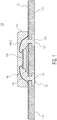
- Fig. 1 is a cross-sectional view of an IC module 100 in accordance with an embodiment of the invention.
- the IC module can be used in a smart card for financial, transportation, security, healthcare, or other applications to store information and perform data processing.
- the IC module has the ability to securely manage, store and provide access to data in the IC module, perform on-module functions, such as encryption, authentication, and authorization, and interact intelligently with a card reader.
- the IC module can communicate with a card reader via electrical contacts.
- the design of the IC module allows the IC module to be made thinner and with lower cost than comparable IC modules.
- the IC module 100 includes a substrate 102, an adhesive material 104, an IC die or chip 106, bond wires 108-1 and 108-2 and an encapsulation 110.
- the IC module is shown in Fig. 1 as including certain components, in other embodiments, the IC module may include fewer components or additional components that are commonly found in conventional IC modules.
- the substrate 102 is a metal leadframe having a first surface 112 on which the IC die is mounted and a second surface 114, which serves as electrical contact areas for signal transmission.
- the metal leadframe is separated into different electrically isolated sections, e.g., sections 116-1 and 116-2, so that the metal leadframe can function as electrical contact pads for the IC module.
- the electrically isolated sections of the metal leadframe will sometime be referred to herein as electrical contact pads.
- electrical contact pads In order to electrically isolate the electrical contact pads, there are spaces or gaps 118 between the electrical contacts.
- the IC module is shown with two contact gaps, which are located below the encapsulation 110 of the IC module. However, the IC module has additional contact gaps, which are not shown in Fig. 1 .
- the contact gaps of the IC module will be further described below with reference to Fig. 2 .
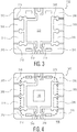
- Fig. 2 is a front side view of the IC module 100 in accordance with an embodiment of the invention.
- the front side of the IC module is the exposed surface of the IC module when the IC module is mounted onto the body of a smart card, which is the second surface 114 depicted in Fig. 1 .
- the IC module includes a number of electrical contact pads 216, which are sections or portions of the metal leadframe 102. These electrical contact pads have gaps 218 between them, which extend throughout the front side of the IC module. In Fig. 2 , all the lines between the contact pads are contact gaps.
- the center region 220 of the IC module is the location of where the IC die 106 is mounted on the other of the metal leadframe and enclosed by the encapsulation 110.
- the contact gaps near the center region will be exposed to the encapsulation.
- the encapsulation will fill these contact gaps when the encapsulation is formed.
- the exposed surfaces of the contact pads may be coated or plated with a non-corrosive conductive material, such as Gold (Au), Silver (Ag), Nickel (Ni), Palladium (Pd) or other appropriate material.
- the metal leadframe 102 is configured or shaped so that at least some of the contact gaps 118 include coining structures 120.
- the coining structures are wider gaps of some of the contact gaps at the second surface 114 of the metal leadframe.
- the coining structures help anchor the encapsulation 110 to the metal leadframe when the encapsulation is formed or solidified in these contact gaps.
- the coining structures can prevent the encapsulation of the IC module 100 from being detached from rest of the IC module.
- the coining structures may be strategically placed so that only portions of the contact gaps that are below or will be filled by the encapsulation will have the coining structures.
- gap width can be designed to be in the range of 1.00 mm to 5.62 mm.
- Coining structure thickness can be in the range of 25% up to 50% of the total thickness of leadframe.
- coining structure width can be over 0.1 mm based on design and coining process technology.
- the metal leadframe 102 can be made of any metal or alloy-based material.
- the metal leadframe may be made of Copper (Cu), Copper-Tin alloy, such as CuSn6, Copper-Iron (CuFe) alloy, Copper Chromium (CuCr) or other appropriate copper alloy or stainless steel.
- the metal leadframe may be formed using stamping technology on reel-to-reel material.
- An example of a stamped metal leadframe 302 that can be used in the IC module 100 in accordance with an embodiment of the invention is shown in Fig. 3 , which is a view of the side on which an IC die is to be mounted on the leadframe.
- the metal leadframe includes a central region 320, where an IC die can be attached.
- the metal leadframe also includes different electrically isolated sections 316, which will be used as contact pads for the resulting IC module. These electrically isolated sections are separated to each other by contact gaps 318.
- the metal leadframe 302 can be made relatively thin.
- a conventional substrate of a smart card module may be 150-170 microns thick, while the metal leadframe may be 60-100 microns thick.
- the overall thickness of the resulting IC module can be significantly reduced when compared to conventional smart card modules.
- the IC die 106 of the IC module 100 is mounted on the metal leadframe 102 using the adhesive material 104.
- the IC die includes circuitry to securely manage, store and provide access to data on the IC module and/or perform on-module functions, such as encryption, authentication, and authorization.
- the IC die is designed to communicate with another device (e.g., a card reader) by electrical contact through the contact pads, which are formed by the sections 116 of the metal leadframes. Thus, electrical connections are required between the IC die and these sections of the metal leadframes.
- the IC die is electrically connected to the sections of the metal leadframes via bond wires 108.
- the bond wires may be made of any suitable metal (e.g., Aluminum or Copper).
- the bond wire 108-1 electrically connects the IC die to the section 116-1 of the metal leadframe
- the bond wire 108-2 electrically connects the IC die to the section 116-2 of the metal leadframe.
- Bond pads may be used to attach the bond wires to the IC die and the metal leadframe.
- the IC module may include additional bond wires.
- the IC module includes a single IC die, which can be access using the contact pads. However, in other embodiments, the IC module may include more than one IC die and may include a contactless interface to access one or more of these IC dies.
- the encapsulation 110 of the IC module 100 is used to protect the bond wires 108 and the IC die 106.
- the encapsulation may be made of any suitable material, such as epoxy mold or molding compound (EMC) or materials used for glob top or dam & fill process.
- EMC epoxy mold or molding compound
- the encapsulation encloses the IC die and the bond wires 108.
- the encapsulation fills in some of the contact gaps 118 with the coining structures 120 around the IC die, as shown in Fig. 1 .
- the remaining contact gaps are also filled with an appropriate filling material, which will prevent adhesive material, e.g., hot melt glue, from seeping through these contact gaps when the IC module is being attached to the body of a smart card.
- the filling material may be the same material used for the encapsulation, such as EMC, or may be a different material.
- the remaining contact gaps that are filled with the filling material are illustrated in Fig. 4 , which is a front side view of the IC module 100 with the metal leadframe 302 depicted in Fig. 3 .
- the front side of the IC module is where the IC die 106 is mounted.
- the encapsulation is shown in phantom so that the underlying components can be seen.
- the contact gaps 318 below the encapsulation, or located within the area of the metal leadframe defined by the encapsulation (i.e., the phantom outline of the encapsulation), will be filled with the encapsulation material when the encapsulation is being formed.
- the contact gaps that are outside of the encapsulation, or located outside of the area of the metal leadframe defined by the encapsulation (i.e., the phantom outline of the encapsulation), will be filled with the filling material, which may be the same material used for the encapsulation.
- all of the contact gaps of the IC module can be substantially filled with the encapsulation material and/or the filling material.
- substantially filled means that more than 90 percent of the contact gaps are filled.
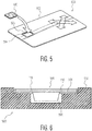
- the IC module 100 can be attached the body 502 of a smart card 500 using an adhesive material 504, e.g., hot melt glue, by placing the adhesive material, in a cavity 506 of the smart card body.
- an adhesive material 504 e.g., hot melt glue
- the adhesive material used to attached the IC module to the smart card body is further illustrated in Fig. 6 , which is a cross-sectional illustration of the IC module attached the smart card body using the adhesive material. If the contact gaps 118 of the IC module are not filled, the adhesive material 504 will seep through the contact gaps, which can cause problems, such as smart cards being glued to other smart cards or to other devices or surfaces.
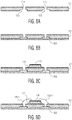
- FIG. 7A A process of manufacturing the IC module 100 in accordance with a first embodiment of the invention is described with reference to Figs. 7A-7D .
- the process of manufacturing the IC module begins by obtaining the metal leadframe 102, which includes contact gaps 118 with coining structures 120 (for at least some of the contact gaps).
- the metal leadframe may be part of a reel-to-reel leadframe.
- the IC die 106 is attached to the metal leadframe using the adhesive material 104.
- the bond wires 108 are attached to the IC die and sections of the metal leadframe to provide electrical connections.
- Fig. 7C the bond wires 108 are attached to the IC die and sections of the metal leadframe to provide electrical connections.
- the material for the encapsulation 100 is dispensed onto the IC die and the bond wires, as well as into all the contact gaps, including the contact gaps that are within and outside of the area defined by the encapsulation. Gaps between contacts are filled by either molding process using epoxy mold compound filling within the mold cavity or dispensing process using thermoplastic materials, such as glob top, along the gap lines. Epoxy mold compound or dispensable thermoplastic material flows into the gaps and fills all over the gap. In the illustrated embodiment, the material is epoxy mold compound (EMC). However, other materials may be used in other embodiments.
- EMC epoxy mold compound
- the encapsulation can be formed, which only fills the contact pads below the encapsulation, i.e., within the area defined by the encapsulation.
- the remaining contact gaps can then be filled in another step using the same or different material with respect to the encapsulation.
- FIG. 8A A process of manufacturing the IC module 100 in accordance with a second embodiment of the invention is described with reference to Figs. 8A-8F .
- the process of manufacturing the IC module begins by obtaining the metal leadframe, which includes contact gaps with coining structures (for at least some of the contact gaps).
- the metal leadframe may be part of a reel-to-reel leadframe.
- a tape 830 is applied to the second surface (or bottom) of the metal leadframe.
- the tape may be a polymide (PI) tape.
- the IC die 106 is attached to the metal leadframe using the adhesive material 104.
- the bond wires 108 are attached to the IC die and sections of the metal leadframe to provide electrical connections.
- the material for the encapsulation 110 is dispensed onto the IC die and the bond wires, as well as into all the contact gaps down to the tape 830 attached to the backside of the metal leadframe.
- the material is epoxy mold compound (EMC).
- EMC epoxy mold compound
- the encapsulation can be formed, which only fills the contact pads below the encapsulation. The remaining contact gaps can then be filled in another step using the same or different material with respect to the encapsulation.
- the tape 830 is removed from the metal leadframe.
- the use of the tape allows the material in the contact pads to have less mold flash on the contact pads or on the front side surface of the metal leadframe. In addition, it prevents or limits contamination from dispensing filled materials in the contact gaps to flow over on other areas on front side surface of the metal leadframe. This results in a reduction of additional cleaning process of the front side of surface to remove unwanted materials.
- Fig. 9 is a process flow diagram of a method for manufacturing an IC module in accordance with an embodiment of the invention.
- a substrate with contact gaps is obtained.
- the substrate may be a metal leadframe with contact gaps.
- an IC die is attached to the substrate.
- electrical connections are made between the IC die and the substrate.
- an encapsulation material is dispensed onto the IC die and into first portions of the contact gaps to form an encapsulation.
- the first portions of the contact gaps are located within an area of the leadframe defined by the encapsulation.
- a filling material is dispensed into second portions of the contact gaps.
- the second portions of the contact gaps are located outside of the area of leadframe defined by the encapsulation.
Landscapes
- Engineering & Computer Science (AREA)
- Microelectronics & Electronic Packaging (AREA)
- Computer Hardware Design (AREA)
- Physics & Mathematics (AREA)
- General Physics & Mathematics (AREA)
- Theoretical Computer Science (AREA)
- Credit Cards Or The Like (AREA)
- Structures Or Materials For Encapsulating Or Coating Semiconductor Devices Or Solid State Devices (AREA)
- Geometry (AREA)
Abstract
Description
- Embodiments of the invention relate generally to electronic circuits and, more particularly, to integrated circuit (IC) modules with multiple electrical contacts and methods for manufacturing such IC modules.
- An IC card, such as a smart card, includes an IC die with circuits that can be used to store information and perform data processing. For example, a portable IC card can be used in financial, transportation, security, healthcare, or other applications to provide identification and authentication.
- The IC die for a smart card is packaged as an IC module, which typically includes the IC die, a substrate and a number of electrical contacts. The IC die is attached to one side of the substrate, while the electrical contacts are attached to the other side of the substrate. Since the electrical contacts need to be electrically isolated from each other, there are gaps between the electrical contacts. The electrical contacts are electrically connected to the IC die via bonding wires through the substrate. The IC die and the bonding wires are encapsulated in an appropriate material to provide structural support and well as protection.
- One consideration in the design of an IC module for a smart card is ensuring that hot melt glue, which is typically used to attach the IC module to the body of the smart card, does not leak through the electrical contact gaps of the IC module, which could cause problems during the manufacturing process of the smart card. Other considerations in the IC module design include reduction of the IC module thickness and lower cost.
- Integrated circuit (IC) modules and methods for manufacturing the IC modules are described. In an embodiment, an IC module includes a substrate with contact gaps on which an IC die is attached with electrical connections between the IC die and the substrate. The IC module further include an encapsulation that encloses the IC die and fills first portions of the contact gaps, where the first portions of the contact gaps are located within an area of the substrate defined by the encapsulation. Second portions of the contact gaps, which are located outside of the area of substrate defined by the encapsulation, are filled with a filling material. In an embodiment, a method for manufacturing an integrated circuit (IC) module includes obtaining a substrate with contact gaps, attaching an IC die to the substrate, making electrical connections between the IC die and the substrate, dispensing an encapsulation material onto the IC die and into first portions of the contact gaps to form an encapsulation, the first portions of the contact gaps being located within an area of the substrate defined by the encapsulation, and dispensing a filling material into second portions of the contact gaps, the second portions of the contact gaps being located outside of the area of substrate defined by the encapsulation.
- In an embodiment, the filling material is the same material as the encapsulation material.
- In an embodiment, the filling material is the same material as the encapsulation material.
- In an embodiment, dispensing the encapsulation material and dispensing the filling material are performed in a single dispensing process.
- In an embodiment, dispensing the encapsulation material and dispensing the filling material are performed so that all the contact gaps are substantially filled with the encapsulation and filling materials.
- In an embodiment, the substrate includes a metal leadframe with the contact gaps. In an embodiment, the metal leadframe is made of Copper, any Copper alloy or stainless steel.
- In an embodiment, at least some of the contact gaps of the metal leadframe include structures to anchor the encapsulation to the metal leadframe.
- In an embodiment, the structures are contiguous with the contact gaps and include wider gaps than the contact gaps.
- In an embodiment, prior to dispensing the encapsulation and filling materials, attaching a tape to a surface of the metal leadframe on the opposite side of the metal leadframe on which the IC die is attached to the metal leadframe.
- In an embodiment, an integrated circuit (IC) module includes a substrate with contact gaps, an IC die attached to the substrate, a plurality of electrical connections between the IC die and the substrate, and an encapsulation that encloses the IC die and fills first portions of the contact gaps, the first portions of the contact gaps being located within an area of the substrate defined by the encapsulation, wherein second portions of the contact gaps are filled with a filling material, the second portions of the contact gaps being located outside of the area of substrate defined by the encapsulation.
- In an embodiment, the filling material is the same material as the encapsulation material.
- In an embodiment, the filling material include epoxy mold compound.
- In an embodiment, all the contact gaps are substantially filled with the encapsulation and filling materials.
- In an embodiment, the substrate includes a metal leadframe with the contact gaps.
- In an embodiment, at least some of the contact gaps of the metal leadframe include structures to anchor the encapsulation to the metal leadframe.
- In an embodiment, the structures are contiguous with the contact gaps and include wider gaps than the contact gaps.
- In an embodiment, an integrated circuit (IC) module includes a metal leadframe with contact gaps, an IC die attached to the metal leadframe, a plurality of bond wires connected to the IC die and the metal leadframe, and an encapsulation that encloses the IC die and fills first portions of the contact gaps, the first portions of the contact gaps being located within an area of the metal leadframe defined by the encapsulation, wherein second portions of the contact gaps are filled with a filling material, the second portions of the contact gaps being located outside of the area of metal leadframe defined by the encapsulation.
- In an embodiment, the filling material include epoxy mold compound.
- In an embodiment, at least some of the contact gaps of the metal leadframe include structures to anchor the encapsulation to the metal leadframe, the structures being contiguous with the contact gaps and including wider gaps than the contact gaps.
- Other aspects and advantages of embodiments of the present invention will become apparent from the following detailed description, taken in conjunction with the accompanying drawings, depicted by way of example of the principles of the invention.
-
Fig. 1 is a cross-sectional view of an IC module in accordance with an embodiment of the invention. -
Fig. 2 is a front side view of the IC module. -
Fig. 3 is a front side view of a metal leadframe of the IC module in accordance with an embodiment of the invention. -
Fig. 4 is a front side view of the IC module with an encapsulation shown in phantom in accordance with an embodiment of the invention. -
Fig. 5 illustrates the IC module being attached to the body of a smart card in accordance with an embodiment of the invention. -
Fig. 6 is a cross-sectional view of the IC module attached to the body of a smart card. -
Figs. 7A-7D illustrate a process of manufacturing the IC module depicted inFig. 1 in accordance with a first embodiment of the invention. -
Figs. 8A-8F illustrate a process of manufacturing the IC module depicted inFig. 1 in accordance with a second embodiment of the invention. -
Fig. 9 is a process flow diagram of a method for manufacturing an IC module in accordance with an embodiment of the invention. - Throughout the description, similar reference numbers may be used to identify similar elements.
- It will be readily understood that the components of the embodiments as generally described herein and illustrated in the appended figures could be arranged and designed in a wide variety of different configurations. Thus, the following detailed description of various embodiments, as represented in the figures, is not intended to limit the scope of the present disclosure, but is merely representative of various embodiments. While the various aspects of the embodiments are presented in drawings, the drawings are not necessarily drawn to scale unless specifically indicated.
- The described embodiments are to be considered in all respects only as illustrative and not restrictive. The scope of the invention is, therefore, indicated by the appended claims rather than by this detailed description. All changes which come within the meaning and range of equivalency of the claims are to be embraced within their scope.
- Reference throughout this specification to features, advantages, or similar language does not imply that all of the features and advantages that may be realized with the present invention should be or are in any single embodiment. Rather, language referring to the features and advantages is understood to mean that a specific feature, advantage, or characteristic described in connection with an embodiment is included in at least one embodiment. Thus, discussions of the features and advantages, and similar language, throughout this specification may, but do not necessarily, refer to the same embodiment.
- Furthermore, the described features, advantages, and characteristics of the invention may be combined in any suitable manner in one or more embodiments. One skilled in the relevant art will recognize, in light of the description herein, that the invention can be practiced without one or more of the specific features or advantages of a particular embodiment. In other instances, additional features and advantages may be recognized in certain embodiments that may not be present in all embodiments of the invention.
- Reference throughout this specification to "one embodiment," "an embodiment," or similar language means that a particular feature, structure, or characteristic described in connection with the indicated embodiment is included in at least one embodiment. Thus, the phrases "in one embodiment," "in an embodiment," and similar language throughout this specification may, but do not necessarily, all refer to the same embodiment.
-
Fig. 1 is a cross-sectional view of anIC module 100 in accordance with an embodiment of the invention. The IC module can be used in a smart card for financial, transportation, security, healthcare, or other applications to store information and perform data processing. In some embodiments, the IC module has the ability to securely manage, store and provide access to data in the IC module, perform on-module functions, such as encryption, authentication, and authorization, and interact intelligently with a card reader. The IC module can communicate with a card reader via electrical contacts. As described in more detail below, the design of the IC module allows the IC module to be made thinner and with lower cost than comparable IC modules. - In the embodiment depicted in
Fig. 1 , theIC module 100 includes asubstrate 102, anadhesive material 104, an IC die orchip 106, bond wires 108-1 and 108-2 and anencapsulation 110. Although the IC module is shown inFig. 1 as including certain components, in other embodiments, the IC module may include fewer components or additional components that are commonly found in conventional IC modules. - In the illustrated embodiment, the
substrate 102 is a metal leadframe having afirst surface 112 on which the IC die is mounted and asecond surface 114, which serves as electrical contact areas for signal transmission. The metal leadframe is separated into different electrically isolated sections, e.g., sections 116-1 and 116-2, so that the metal leadframe can function as electrical contact pads for the IC module. Thus, the electrically isolated sections of the metal leadframe will sometime be referred to herein as electrical contact pads. In order to electrically isolate the electrical contact pads, there are spaces orgaps 118 between the electrical contacts. InFig. 1 , the IC module is shown with two contact gaps, which are located below theencapsulation 110 of the IC module. However, the IC module has additional contact gaps, which are not shown inFig. 1 . The contact gaps of the IC module will be further described below with reference toFig. 2 . -
Fig. 2 is a front side view of theIC module 100 in accordance with an embodiment of the invention. The front side of the IC module is the exposed surface of the IC module when the IC module is mounted onto the body of a smart card, which is thesecond surface 114 depicted inFig. 1 . As shown inFig. 2 , the IC module includes a number ofelectrical contact pads 216, which are sections or portions of themetal leadframe 102. These electrical contact pads havegaps 218 between them, which extend throughout the front side of the IC module. InFig. 2 , all the lines between the contact pads are contact gaps. Thecenter region 220 of the IC module is the location of where the IC die 106 is mounted on the other of the metal leadframe and enclosed by theencapsulation 110. Thus, the contact gaps near the center region will be exposed to the encapsulation. In other words, the encapsulation will fill these contact gaps when the encapsulation is formed. In some embodiments, the exposed surfaces of the contact pads may be coated or plated with a non-corrosive conductive material, such as Gold (Au), Silver (Ag), Nickel (Ni), Palladium (Pd) or other appropriate material. - Turning back to
Fig. 1 , in the illustrated embodiment, themetal leadframe 102 is configured or shaped so that at least some of thecontact gaps 118 include coiningstructures 120. As shown inFig. 1 , the coining structures are wider gaps of some of the contact gaps at thesecond surface 114 of the metal leadframe. The coining structures help anchor theencapsulation 110 to the metal leadframe when the encapsulation is formed or solidified in these contact gaps. Thus, the coining structures can prevent the encapsulation of theIC module 100 from being detached from rest of the IC module. The coining structures may be strategically placed so that only portions of the contact gaps that are below or will be filled by the encapsulation will have the coining structures. With different outlines and sizes of the IC module, gap width can be designed to be in the range of 1.00 mm to 5.62 mm. Coining structure thickness can be in the range of 25% up to 50% of the total thickness of leadframe. In addition, coining structure width can be over 0.1 mm based on design and coining process technology. - The
metal leadframe 102 can be made of any metal or alloy-based material. As an example, the metal leadframe may be made of Copper (Cu), Copper-Tin alloy, such as CuSn6, Copper-Iron (CuFe) alloy, Copper Chromium (CuCr) or other appropriate copper alloy or stainless steel. The metal leadframe may be formed using stamping technology on reel-to-reel material. An example of a stampedmetal leadframe 302 that can be used in theIC module 100 in accordance with an embodiment of the invention is shown inFig. 3 , which is a view of the side on which an IC die is to be mounted on the leadframe. As shown inFig. 3 , the metal leadframe includes acentral region 320, where an IC die can be attached. The metal leadframe also includes different electricallyisolated sections 316, which will be used as contact pads for the resulting IC module. These electrically isolated sections are separated to each other bycontact gaps 318. - Unlike a conventional substrate of a smart card module that includes thick glass-epoxy structure with a metal layer for the contact pads, the
metal leadframe 302 can be made relatively thin. As an example, a conventional substrate of a smart card module may be 150-170 microns thick, while the metal leadframe may be 60-100 microns thick. Thus, the overall thickness of the resulting IC module can be significantly reduced when compared to conventional smart card modules. - Turning back to
Fig. 1 , the IC die 106 of theIC module 100 is mounted on themetal leadframe 102 using theadhesive material 104. The IC die includes circuitry to securely manage, store and provide access to data on the IC module and/or perform on-module functions, such as encryption, authentication, and authorization. The IC die is designed to communicate with another device (e.g., a card reader) by electrical contact through the contact pads, which are formed by thesections 116 of the metal leadframes. Thus, electrical connections are required between the IC die and these sections of the metal leadframes. In the illustrated embodiment, the IC die is electrically connected to the sections of the metal leadframes via bond wires 108. The bond wires may be made of any suitable metal (e.g., Aluminum or Copper). In the embodiment depicted inFig. 1 , the bond wire 108-1 electrically connects the IC die to the section 116-1 of the metal leadframe, while the bond wire 108-2 electrically connects the IC die to the section 116-2 of the metal leadframe. Bond pads may be used to attach the bond wires to the IC die and the metal leadframe. Although only two bond wires are illustrated inFig. 1 , the IC module may include additional bond wires. Also, in the embodiment depicted inFig. 1 , the IC module includes a single IC die, which can be access using the contact pads. However, in other embodiments, the IC module may include more than one IC die and may include a contactless interface to access one or more of these IC dies. - The
encapsulation 110 of theIC module 100 is used to protect the bond wires 108 and the IC die 106. The encapsulation may be made of any suitable material, such as epoxy mold or molding compound (EMC) or materials used for glob top or dam & fill process. The encapsulation encloses the IC die and the bond wires 108. In addition, the encapsulation fills in some of thecontact gaps 118 with the coiningstructures 120 around the IC die, as shown inFig. 1 . The remaining contact gaps are also filled with an appropriate filling material, which will prevent adhesive material, e.g., hot melt glue, from seeping through these contact gaps when the IC module is being attached to the body of a smart card. The filling material may be the same material used for the encapsulation, such as EMC, or may be a different material. The remaining contact gaps that are filled with the filling material are illustrated inFig. 4 , which is a front side view of theIC module 100 with themetal leadframe 302 depicted inFig. 3 . The front side of the IC module is where the IC die 106 is mounted. InFig. 4 , the encapsulation is shown in phantom so that the underlying components can be seen. Thecontact gaps 318 below the encapsulation, or located within the area of the metal leadframe defined by the encapsulation (i.e., the phantom outline of the encapsulation), will be filled with the encapsulation material when the encapsulation is being formed. The contact gaps that are outside of the encapsulation, or located outside of the area of the metal leadframe defined by the encapsulation (i.e., the phantom outline of the encapsulation), will be filled with the filling material, which may be the same material used for the encapsulation. Thus, all of the contact gaps of the IC module can be substantially filled with the encapsulation material and/or the filling material. As used herein, "substantially filled" means that more than 90 percent of the contact gaps are filled. - As illustrated in
Fig. 5 , theIC module 100 can be attached thebody 502 of asmart card 500 using anadhesive material 504, e.g., hot melt glue, by placing the adhesive material, in acavity 506 of the smart card body. The adhesive material used to attached the IC module to the smart card body is further illustrated inFig. 6 , which is a cross-sectional illustration of the IC module attached the smart card body using the adhesive material. If thecontact gaps 118 of the IC module are not filled, theadhesive material 504 will seep through the contact gaps, which can cause problems, such as smart cards being glued to other smart cards or to other devices or surfaces. - A process of manufacturing the
IC module 100 in accordance with a first embodiment of the invention is described with reference toFigs. 7A-7D . As illustrated inFig. 7A , the process of manufacturing the IC module begins by obtaining themetal leadframe 102, which includescontact gaps 118 with coining structures 120 (for at least some of the contact gaps). In some embodiments, the metal leadframe may be part of a reel-to-reel leadframe. Next, as illustrated inFig. 7B , the IC die 106 is attached to the metal leadframe using theadhesive material 104. Next, as illustrated inFig. 7C , the bond wires 108 are attached to the IC die and sections of the metal leadframe to provide electrical connections. Next, as illustrated inFig. 7D , the material for theencapsulation 100 is dispensed onto the IC die and the bond wires, as well as into all the contact gaps, including the contact gaps that are within and outside of the area defined by the encapsulation. Gaps between contacts are filled by either molding process using epoxy mold compound filling within the mold cavity or dispensing process using thermoplastic materials, such as glob top, along the gap lines. Epoxy mold compound or dispensable thermoplastic material flows into the gaps and fills all over the gap. In the illustrated embodiment, the material is epoxy mold compound (EMC). However, other materials may be used in other embodiments. In some alternative embodiments, the encapsulation can be formed, which only fills the contact pads below the encapsulation, i.e., within the area defined by the encapsulation. The remaining contact gaps can then be filled in another step using the same or different material with respect to the encapsulation. - A process of manufacturing the
IC module 100 in accordance with a second embodiment of the invention is described with reference toFigs. 8A-8F . As illustrated inFig. 8A , the process of manufacturing the IC module begins by obtaining the metal leadframe, which includes contact gaps with coining structures (for at least some of the contact gaps). In some embodiments, the metal leadframe may be part of a reel-to-reel leadframe. Next, as illustrated inFig. 8B , atape 830 is applied to the second surface (or bottom) of the metal leadframe. As an example, the tape may be a polymide (PI) tape. Next, as illustrated inFig. 8C , the IC die 106 is attached to the metal leadframe using theadhesive material 104. Next, as illustrated inFig. 8D , the bond wires 108 are attached to the IC die and sections of the metal leadframe to provide electrical connections. Next, as illustrated inFig. 8E , the material for theencapsulation 110 is dispensed onto the IC die and the bond wires, as well as into all the contact gaps down to thetape 830 attached to the backside of the metal leadframe. In the illustrated embodiment, the material is epoxy mold compound (EMC). However, other materials may be used in other embodiments. In some alternative embodiments, the encapsulation can be formed, which only fills the contact pads below the encapsulation. The remaining contact gaps can then be filled in another step using the same or different material with respect to the encapsulation. Next, as illustrated inFig. 8F , thetape 830 is removed from the metal leadframe. The use of the tape allows the material in the contact pads to have less mold flash on the contact pads or on the front side surface of the metal leadframe. In addition, it prevents or limits contamination from dispensing filled materials in the contact gaps to flow over on other areas on front side surface of the metal leadframe. This results in a reduction of additional cleaning process of the front side of surface to remove unwanted materials. -
Fig. 9 is a process flow diagram of a method for manufacturing an IC module in accordance with an embodiment of the invention. Atblock 902, a substrate with contact gaps is obtained. The substrate may be a metal leadframe with contact gaps. Next, atblock 904, an IC die is attached to the substrate. Next, atblock 906, electrical connections are made between the IC die and the substrate. Next, atblock 908, an encapsulation material is dispensed onto the IC die and into first portions of the contact gaps to form an encapsulation. The first portions of the contact gaps are located within an area of the leadframe defined by the encapsulation. Next, atblock 910, a filling material is dispensed into second portions of the contact gaps. The second portions of the contact gaps are located outside of the area of leadframe defined by the encapsulation. - Although the operations of the method herein are shown and described in a particular order, the order of the operations of the method may be altered so that certain operations may be performed in an inverse order or so that certain operations may be performed, at least in part, concurrently with other operations. In another embodiment, instructions or sub-operations of distinct operations may be implemented in an intermittent and/or alternating manner.
- In addition, although specific embodiments of the invention that have been described or depicted include several components described or depicted herein, other embodiments of the invention may include fewer or more components to implement less or more feature.
- Furthermore, although specific embodiments of the invention have been described and depicted, the invention is not to be limited to the specific forms or arrangements of parts so described and depicted. The scope of the invention is to be defined by the claims appended hereto and their equivalents.
Claims (15)
- A method for manufacturing an integrated circuit (IC) module, the method comprising:obtaining a substrate (102) with contact gaps (118, 318);attaching an IC die (106) to the substrate;making electrical connections between the IC die and the substrate;dispensing an encapsulation material onto the IC die and into first portions of the contact gaps to form an encapsulation, the first portions of the contact gaps being located within an area of the substrate defined by the encapsulation; anddispensing a filling material into second portions of the contact gaps, the second portions of the contact gaps being located outside of the area of substrate defined by the encapsulation.
- The method of claim 1, wherein the filling material is the same material as the encapsulation material.
- The method of claim 1 or claim 2, wherein the filling material include epoxy mold compound.
- The method of any one of the claims 1 to 3, wherein dispensing the encapsulation material and dispensing the filling material are performed in a single dispensing process.
- The method of any one of the claims 1 to 4, wherein dispensing the encapsulation material and dispensing the filling material are performed so that all the contact gaps are substantially filled with the encapsulation and filling materials.
- The method of any one of the claims 1 to 5, wherein the substrate includes a metal leadframe with the contact gaps.
- The method of claim 6, wherein at least some of the contact gaps of the metal leadframe include structures to anchor the encapsulation to the metal leadframe, wherein the structures are contiguous with the contact gaps and include wider gaps than the contact gaps.
- The method of claim 6 or claim 7, prior to dispensing the encapsulation and filling materials, attaching a tape to a surface of the metal leadframe on the opposite side of the metal leadframe on which the IC die is attached to the metal leadframe.
- An integrated circuit (IC) module comprising:a substrate with contact gaps;an IC die attached to the substrate;a plurality of electrical connections between the IC die and the substrate; andan encapsulation that encloses the IC die and fills first portions of the contact gaps, the first portions of the contact gaps being located within an area of the substrate defined by the encapsulation,wherein second portions of the contact gaps are filled with a filling material, the second portions of the contact gaps being located outside of the area of substrate defined by the encapsulation.
- The IC module of claim 9, wherein the filling material is the same material as the encapsulation material.
- The IC module of claim 9 or claim 10, wherein the filling material include epoxy mold compound.
- The IC module of any one of the claims 9 to 11, wherein all the contact gaps are substantially filled with the encapsulation and filling materials.
- The IC module of any one of the claims 9 to 12, wherein the substrate includes a metal leadframe with the contact gaps.
- The IC module of claim 13, wherein at least some of the contact gaps of the metal leadframe include structures to anchor the encapsulation to the metal leadframe.
- The IC module of claim 13 or claim 14, wherein the structures are contiguous with the contact gaps and include wider gaps than the contact gaps.
Applications Claiming Priority (1)
| Application Number | Priority Date | Filing Date | Title |
|---|---|---|---|
| US15/178,329 US9595455B1 (en) | 2016-06-09 | 2016-06-09 | Integrated circuit module with filled contact gaps |
Publications (2)
| Publication Number | Publication Date |
|---|---|
| EP3255587A1 true EP3255587A1 (en) | 2017-12-13 |
| EP3255587B1 EP3255587B1 (en) | 2021-03-10 |
Family
ID=58046473
Family Applications (1)
| Application Number | Title | Priority Date | Filing Date |
|---|---|---|---|
| EP17153815.0A Active EP3255587B1 (en) | 2016-06-09 | 2017-01-30 | Integrated circuit module with filled contact gaps |
Country Status (3)
| Country | Link |
|---|---|
| US (1) | US9595455B1 (en) |
| EP (1) | EP3255587B1 (en) |
| CN (1) | CN107492504A (en) |
Cited By (1)
| Publication number | Priority date | Publication date | Assignee | Title |
|---|---|---|---|---|
| EP4002446A4 (en) * | 2019-07-19 | 2023-09-06 | Guangdong Chippacking Technology Co., Ltd. | HIGH DENSITY EXPOSED MULTIFACE PIN ENCAPSULATION STRUCTURE AND PRODUCTION METHOD THEREFOR |
Families Citing this family (2)
| Publication number | Priority date | Publication date | Assignee | Title |
|---|---|---|---|---|
| US10847385B2 (en) * | 2018-10-09 | 2020-11-24 | Nxp B.V. | Glob top encapsulation using molding tape |
| US10763203B1 (en) * | 2019-02-08 | 2020-09-01 | Nxp B.V. | Conductive trace design for smart card |
Citations (3)
| Publication number | Priority date | Publication date | Assignee | Title |
|---|---|---|---|---|
| US6281568B1 (en) * | 1998-10-21 | 2001-08-28 | Amkor Technology, Inc. | Plastic integrated circuit device package and leadframe having partially undercut leads and die pad |
| US20140239471A1 (en) * | 2013-02-28 | 2014-08-28 | Nxp B.V. | Ic package with stainless steel leadframe |
| US20150001698A1 (en) * | 2013-06-28 | 2015-01-01 | Stmicroelectronics, Inc. | Leadless packages and method of manufacturing same |
Family Cites Families (18)
| Publication number | Priority date | Publication date | Assignee | Title |
|---|---|---|---|---|
| FR2659157B2 (en) | 1989-05-26 | 1994-09-30 | Lemaire Gerard | METHOD FOR MANUFACTURING A CARD, SAID CARD, AND CARD OBTAINED BY THIS PROCESS. |
| DE19721281C2 (en) | 1997-05-21 | 1999-04-01 | Ods Landis & Gyr Gmbh & Co Kg | Chip module for a chip card |
| DE19800646C2 (en) | 1998-01-09 | 2000-05-04 | Siemens Ag | Carrier element for a semiconductor chip |
| WO1999059205A1 (en) * | 1998-05-12 | 1999-11-18 | Mitsubishi Gas Chemical Company, Inc. | Semiconductor plastic package and method for producing printed wiring board |
| TW419795B (en) * | 1998-08-20 | 2001-01-21 | Mitsubishi Gas Chemical Co | Semiconductor plastic package and method of producing printed wiring board |
| TW575949B (en) * | 2001-02-06 | 2004-02-11 | Hitachi Ltd | Mixed integrated circuit device, its manufacturing method and electronic apparatus |
| US20020180014A1 (en) * | 2001-06-02 | 2002-12-05 | Philpot Kenneth R. | Enhanced performance surface mount semiconductor package devices and methods |
| US7176582B2 (en) | 2002-04-11 | 2007-02-13 | Nxp B.V. | Semiconductor device and method of manufacturing same |
| US6903449B2 (en) * | 2003-08-01 | 2005-06-07 | Micron Technology, Inc. | Semiconductor component having chip on board leadframe |
| EP1655691A1 (en) | 2004-11-08 | 2006-05-10 | Axalto SA | A smart card micro-electronic module manufacturing method |
| TW200721426A (en) | 2005-07-25 | 2007-06-01 | Koninkl Philips Electronics Nv | Air cavity package for flip-chip |
| JP5407474B2 (en) * | 2009-03-25 | 2014-02-05 | 凸版印刷株式会社 | Manufacturing method of semiconductor element substrate |
| JP5051189B2 (en) * | 2009-07-10 | 2012-10-17 | アイシン・エィ・ダブリュ株式会社 | Electronic circuit equipment |
| TWI429043B (en) * | 2010-04-26 | 2014-03-01 | 聯致科技股份有限公司 | Circuit board structure, packaging structure and method for making the same |
| TWI445103B (en) * | 2010-08-19 | 2014-07-11 | 乾坤科技股份有限公司 | Electronic package structure and packaging method thereof |
| CN103022011B (en) * | 2011-09-23 | 2015-10-07 | 讯芯电子科技(中山)有限公司 | Semiconductor package and manufacture method thereof |
| CN102543937B (en) * | 2011-12-30 | 2014-01-22 | 北京工业大学 | Flip chip on-chip package and manufacturing method thereof |
| US10586771B2 (en) * | 2013-12-16 | 2020-03-10 | Utac Headquarters Pte, Ltd | Conductive shield for semiconductor package |
-
2016
- 2016-06-09 US US15/178,329 patent/US9595455B1/en active Active
-
2017
- 2017-01-22 CN CN201710046800.0A patent/CN107492504A/en active Pending
- 2017-01-30 EP EP17153815.0A patent/EP3255587B1/en active Active
Patent Citations (3)
| Publication number | Priority date | Publication date | Assignee | Title |
|---|---|---|---|---|
| US6281568B1 (en) * | 1998-10-21 | 2001-08-28 | Amkor Technology, Inc. | Plastic integrated circuit device package and leadframe having partially undercut leads and die pad |
| US20140239471A1 (en) * | 2013-02-28 | 2014-08-28 | Nxp B.V. | Ic package with stainless steel leadframe |
| US20150001698A1 (en) * | 2013-06-28 | 2015-01-01 | Stmicroelectronics, Inc. | Leadless packages and method of manufacturing same |
Cited By (1)
| Publication number | Priority date | Publication date | Assignee | Title |
|---|---|---|---|---|
| EP4002446A4 (en) * | 2019-07-19 | 2023-09-06 | Guangdong Chippacking Technology Co., Ltd. | HIGH DENSITY EXPOSED MULTIFACE PIN ENCAPSULATION STRUCTURE AND PRODUCTION METHOD THEREFOR |
Also Published As
| Publication number | Publication date |
|---|---|
| US9595455B1 (en) | 2017-03-14 |
| EP3255587B1 (en) | 2021-03-10 |
| CN107492504A (en) | 2017-12-19 |
Similar Documents
| Publication | Publication Date | Title |
|---|---|---|
| US6861734B2 (en) | Resin-molded semiconductor device | |
| US9287200B2 (en) | Packaged semiconductor device | |
| US10727169B2 (en) | Semiconductor device having lead with back and end surfaces provided with plating layers | |
| US9859197B2 (en) | Integrated circuit package fabrication | |
| US20080197479A1 (en) | Semiconductor package, integrated circuit cards incorporating the semiconductor package, and method of manufacturing the same | |
| US20060151858A1 (en) | Leadframe and semiconductor package made using the leadframe | |
| EP0942392A2 (en) | Chip card | |
| CN101416311B (en) | Clipless and wireless semiconductor die package and method for making the same | |
| US20100314728A1 (en) | Ic package having an inductor etched into a leadframe thereof | |
| US20180122731A1 (en) | Plated ditch pre-mold lead frame, semiconductor package, and method of making same | |
| US20180233438A1 (en) | Leadframe, semiconductor package including a leadframe and method for forming a semiconductor package | |
| EP3255587B1 (en) | Integrated circuit module with filled contact gaps | |
| US9349940B2 (en) | Semiconductor device and method of manufacturing the same | |
| US10763203B1 (en) | Conductive trace design for smart card | |
| US8698288B1 (en) | Flexible substrate with crimping interconnection | |
| US7915739B2 (en) | Method and arrangement for contact-connecting semiconductor chips on a metallic substrate | |
| JP2017038051A (en) | Semiconductor package and manufacturing method of the same | |
| EP0723293B1 (en) | Semiconductor device with a heat sink and method of producing the heat sink | |
| US20060261456A1 (en) | Micromodule, particularly for chip card | |
| JP3842241B2 (en) | Semiconductor device | |
| JP2003168776A (en) | Resin-sealed semiconductor device | |
| JPS61279141A (en) | Direct connection apparatus and method for lead frame with flexible tapered lead and mechanical die support | |
| US20030122224A1 (en) | Lead frame with dual thin film coated on inner lead terminal | |
| CN111341748B (en) | Selectively patterned leadframes | |
| US20090026630A1 (en) | Semiconductor device and method for manufacturing same |
Legal Events
| Date | Code | Title | Description |
|---|---|---|---|
| PUAI | Public reference made under article 153(3) epc to a published international application that has entered the european phase |
Free format text: ORIGINAL CODE: 0009012 |
|
| STAA | Information on the status of an ep patent application or granted ep patent |
Free format text: STATUS: THE APPLICATION HAS BEEN PUBLISHED |
|
| AK | Designated contracting states |
Kind code of ref document: A1 Designated state(s): AL AT BE BG CH CY CZ DE DK EE ES FI FR GB GR HR HU IE IS IT LI LT LU LV MC MK MT NL NO PL PT RO RS SE SI SK SM TR |
|
| AX | Request for extension of the european patent |
Extension state: BA ME |
|
| STAA | Information on the status of an ep patent application or granted ep patent |
Free format text: STATUS: REQUEST FOR EXAMINATION WAS MADE |
|
| 17P | Request for examination filed |
Effective date: 20180613 |
|
| RBV | Designated contracting states (corrected) |
Designated state(s): AL AT BE BG CH CY CZ DE DK EE ES FI FR GB GR HR HU IE IS IT LI LT LU LV MC MK MT NL NO PL PT RO RS SE SI SK SM TR |
|
| STAA | Information on the status of an ep patent application or granted ep patent |
Free format text: STATUS: EXAMINATION IS IN PROGRESS |
|
| 17Q | First examination report despatched |
Effective date: 20190301 |
|
| GRAP | Despatch of communication of intention to grant a patent |
Free format text: ORIGINAL CODE: EPIDOSNIGR1 |
|
| STAA | Information on the status of an ep patent application or granted ep patent |
Free format text: STATUS: GRANT OF PATENT IS INTENDED |
|
| INTG | Intention to grant announced |
Effective date: 20201021 |
|
| GRAS | Grant fee paid |
Free format text: ORIGINAL CODE: EPIDOSNIGR3 |
|
| GRAA | (expected) grant |
Free format text: ORIGINAL CODE: 0009210 |
|
| STAA | Information on the status of an ep patent application or granted ep patent |
Free format text: STATUS: THE PATENT HAS BEEN GRANTED |
|
| AK | Designated contracting states |
Kind code of ref document: B1 Designated state(s): AL AT BE BG CH CY CZ DE DK EE ES FI FR GB GR HR HU IE IS IT LI LT LU LV MC MK MT NL NO PL PT RO RS SE SI SK SM TR |
|
| REG | Reference to a national code |
Ref country code: GB Ref legal event code: FG4D |
|
| REG | Reference to a national code |
Ref country code: AT Ref legal event code: REF Ref document number: 1370654 Country of ref document: AT Kind code of ref document: T Effective date: 20210315 Ref country code: CH Ref legal event code: EP |
|
| REG | Reference to a national code |
Ref country code: IE Ref legal event code: FG4D |
|
| REG | Reference to a national code |
Ref country code: DE Ref legal event code: R096 Ref document number: 602017034144 Country of ref document: DE |
|
| REG | Reference to a national code |
Ref country code: LT Ref legal event code: MG9D |
|
| PG25 | Lapsed in a contracting state [announced via postgrant information from national office to epo] |
Ref country code: HR Free format text: LAPSE BECAUSE OF FAILURE TO SUBMIT A TRANSLATION OF THE DESCRIPTION OR TO PAY THE FEE WITHIN THE PRESCRIBED TIME-LIMIT Effective date: 20210310 Ref country code: GR Free format text: LAPSE BECAUSE OF FAILURE TO SUBMIT A TRANSLATION OF THE DESCRIPTION OR TO PAY THE FEE WITHIN THE PRESCRIBED TIME-LIMIT Effective date: 20210611 Ref country code: FI Free format text: LAPSE BECAUSE OF FAILURE TO SUBMIT A TRANSLATION OF THE DESCRIPTION OR TO PAY THE FEE WITHIN THE PRESCRIBED TIME-LIMIT Effective date: 20210310 Ref country code: NO Free format text: LAPSE BECAUSE OF FAILURE TO SUBMIT A TRANSLATION OF THE DESCRIPTION OR TO PAY THE FEE WITHIN THE PRESCRIBED TIME-LIMIT Effective date: 20210610 Ref country code: BG Free format text: LAPSE BECAUSE OF FAILURE TO SUBMIT A TRANSLATION OF THE DESCRIPTION OR TO PAY THE FEE WITHIN THE PRESCRIBED TIME-LIMIT Effective date: 20210610 Ref country code: LT Free format text: LAPSE BECAUSE OF FAILURE TO SUBMIT A TRANSLATION OF THE DESCRIPTION OR TO PAY THE FEE WITHIN THE PRESCRIBED TIME-LIMIT Effective date: 20210310 |
|
| REG | Reference to a national code |
Ref country code: AT Ref legal event code: MK05 Ref document number: 1370654 Country of ref document: AT Kind code of ref document: T Effective date: 20210310 |
|
| REG | Reference to a national code |
Ref country code: NL Ref legal event code: MP Effective date: 20210310 |
|
| PG25 | Lapsed in a contracting state [announced via postgrant information from national office to epo] |
Ref country code: SE Free format text: LAPSE BECAUSE OF FAILURE TO SUBMIT A TRANSLATION OF THE DESCRIPTION OR TO PAY THE FEE WITHIN THE PRESCRIBED TIME-LIMIT Effective date: 20210310 Ref country code: RS Free format text: LAPSE BECAUSE OF FAILURE TO SUBMIT A TRANSLATION OF THE DESCRIPTION OR TO PAY THE FEE WITHIN THE PRESCRIBED TIME-LIMIT Effective date: 20210310 Ref country code: LV Free format text: LAPSE BECAUSE OF FAILURE TO SUBMIT A TRANSLATION OF THE DESCRIPTION OR TO PAY THE FEE WITHIN THE PRESCRIBED TIME-LIMIT Effective date: 20210310 |
|
| PG25 | Lapsed in a contracting state [announced via postgrant information from national office to epo] |
Ref country code: NL Free format text: LAPSE BECAUSE OF FAILURE TO SUBMIT A TRANSLATION OF THE DESCRIPTION OR TO PAY THE FEE WITHIN THE PRESCRIBED TIME-LIMIT Effective date: 20210310 |
|
| PG25 | Lapsed in a contracting state [announced via postgrant information from national office to epo] |
Ref country code: SM Free format text: LAPSE BECAUSE OF FAILURE TO SUBMIT A TRANSLATION OF THE DESCRIPTION OR TO PAY THE FEE WITHIN THE PRESCRIBED TIME-LIMIT Effective date: 20210310 Ref country code: AT Free format text: LAPSE BECAUSE OF FAILURE TO SUBMIT A TRANSLATION OF THE DESCRIPTION OR TO PAY THE FEE WITHIN THE PRESCRIBED TIME-LIMIT Effective date: 20210310 Ref country code: CZ Free format text: LAPSE BECAUSE OF FAILURE TO SUBMIT A TRANSLATION OF THE DESCRIPTION OR TO PAY THE FEE WITHIN THE PRESCRIBED TIME-LIMIT Effective date: 20210310 Ref country code: EE Free format text: LAPSE BECAUSE OF FAILURE TO SUBMIT A TRANSLATION OF THE DESCRIPTION OR TO PAY THE FEE WITHIN THE PRESCRIBED TIME-LIMIT Effective date: 20210310 |
|
| PG25 | Lapsed in a contracting state [announced via postgrant information from national office to epo] |
Ref country code: RO Free format text: LAPSE BECAUSE OF FAILURE TO SUBMIT A TRANSLATION OF THE DESCRIPTION OR TO PAY THE FEE WITHIN THE PRESCRIBED TIME-LIMIT Effective date: 20210310 Ref country code: SK Free format text: LAPSE BECAUSE OF FAILURE TO SUBMIT A TRANSLATION OF THE DESCRIPTION OR TO PAY THE FEE WITHIN THE PRESCRIBED TIME-LIMIT Effective date: 20210310 Ref country code: PL Free format text: LAPSE BECAUSE OF FAILURE TO SUBMIT A TRANSLATION OF THE DESCRIPTION OR TO PAY THE FEE WITHIN THE PRESCRIBED TIME-LIMIT Effective date: 20210310 Ref country code: PT Free format text: LAPSE BECAUSE OF FAILURE TO SUBMIT A TRANSLATION OF THE DESCRIPTION OR TO PAY THE FEE WITHIN THE PRESCRIBED TIME-LIMIT Effective date: 20210712 Ref country code: IS Free format text: LAPSE BECAUSE OF FAILURE TO SUBMIT A TRANSLATION OF THE DESCRIPTION OR TO PAY THE FEE WITHIN THE PRESCRIBED TIME-LIMIT Effective date: 20210710 |
|
| REG | Reference to a national code |
Ref country code: DE Ref legal event code: R097 Ref document number: 602017034144 Country of ref document: DE |
|
| PLBE | No opposition filed within time limit |
Free format text: ORIGINAL CODE: 0009261 |
|
| STAA | Information on the status of an ep patent application or granted ep patent |
Free format text: STATUS: NO OPPOSITION FILED WITHIN TIME LIMIT |
|
| PG25 | Lapsed in a contracting state [announced via postgrant information from national office to epo] |
Ref country code: ES Free format text: LAPSE BECAUSE OF FAILURE TO SUBMIT A TRANSLATION OF THE DESCRIPTION OR TO PAY THE FEE WITHIN THE PRESCRIBED TIME-LIMIT Effective date: 20210310 Ref country code: DK Free format text: LAPSE BECAUSE OF FAILURE TO SUBMIT A TRANSLATION OF THE DESCRIPTION OR TO PAY THE FEE WITHIN THE PRESCRIBED TIME-LIMIT Effective date: 20210310 Ref country code: AL Free format text: LAPSE BECAUSE OF FAILURE TO SUBMIT A TRANSLATION OF THE DESCRIPTION OR TO PAY THE FEE WITHIN THE PRESCRIBED TIME-LIMIT Effective date: 20210310 |
|
| 26N | No opposition filed |
Effective date: 20211213 |
|
| PG25 | Lapsed in a contracting state [announced via postgrant information from national office to epo] |
Ref country code: SI Free format text: LAPSE BECAUSE OF FAILURE TO SUBMIT A TRANSLATION OF THE DESCRIPTION OR TO PAY THE FEE WITHIN THE PRESCRIBED TIME-LIMIT Effective date: 20210310 |
|
| PG25 | Lapsed in a contracting state [announced via postgrant information from national office to epo] |
Ref country code: IT Free format text: LAPSE BECAUSE OF FAILURE TO SUBMIT A TRANSLATION OF THE DESCRIPTION OR TO PAY THE FEE WITHIN THE PRESCRIBED TIME-LIMIT Effective date: 20210310 |
|
| PG25 | Lapsed in a contracting state [announced via postgrant information from national office to epo] |
Ref country code: IS Free format text: LAPSE BECAUSE OF FAILURE TO SUBMIT A TRANSLATION OF THE DESCRIPTION OR TO PAY THE FEE WITHIN THE PRESCRIBED TIME-LIMIT Effective date: 20210710 |
|
| PG25 | Lapsed in a contracting state [announced via postgrant information from national office to epo] |
Ref country code: MC Free format text: LAPSE BECAUSE OF FAILURE TO SUBMIT A TRANSLATION OF THE DESCRIPTION OR TO PAY THE FEE WITHIN THE PRESCRIBED TIME-LIMIT Effective date: 20210310 |
|
| REG | Reference to a national code |
Ref country code: CH Ref legal event code: PL |
|
| GBPC | Gb: european patent ceased through non-payment of renewal fee |
Effective date: 20220130 |
|
| REG | Reference to a national code |
Ref country code: BE Ref legal event code: MM Effective date: 20220131 |
|
| PG25 | Lapsed in a contracting state [announced via postgrant information from national office to epo] |
Ref country code: LU Free format text: LAPSE BECAUSE OF NON-PAYMENT OF DUE FEES Effective date: 20220130 Ref country code: GB Free format text: LAPSE BECAUSE OF NON-PAYMENT OF DUE FEES Effective date: 20220130 |
|
| PG25 | Lapsed in a contracting state [announced via postgrant information from national office to epo] |
Ref country code: BE Free format text: LAPSE BECAUSE OF NON-PAYMENT OF DUE FEES Effective date: 20220131 |
|
| PG25 | Lapsed in a contracting state [announced via postgrant information from national office to epo] |
Ref country code: LI Free format text: LAPSE BECAUSE OF NON-PAYMENT OF DUE FEES Effective date: 20220131 Ref country code: CH Free format text: LAPSE BECAUSE OF NON-PAYMENT OF DUE FEES Effective date: 20220131 |
|
| PG25 | Lapsed in a contracting state [announced via postgrant information from national office to epo] |
Ref country code: IE Free format text: LAPSE BECAUSE OF NON-PAYMENT OF DUE FEES Effective date: 20220130 |
|
| P01 | Opt-out of the competence of the unified patent court (upc) registered |
Effective date: 20230725 |
|
| PG25 | Lapsed in a contracting state [announced via postgrant information from national office to epo] |
Ref country code: HU Free format text: LAPSE BECAUSE OF FAILURE TO SUBMIT A TRANSLATION OF THE DESCRIPTION OR TO PAY THE FEE WITHIN THE PRESCRIBED TIME-LIMIT; INVALID AB INITIO Effective date: 20170130 |
|
| PG25 | Lapsed in a contracting state [announced via postgrant information from national office to epo] |
Ref country code: MK Free format text: LAPSE BECAUSE OF FAILURE TO SUBMIT A TRANSLATION OF THE DESCRIPTION OR TO PAY THE FEE WITHIN THE PRESCRIBED TIME-LIMIT Effective date: 20210310 Ref country code: CY Free format text: LAPSE BECAUSE OF FAILURE TO SUBMIT A TRANSLATION OF THE DESCRIPTION OR TO PAY THE FEE WITHIN THE PRESCRIBED TIME-LIMIT Effective date: 20210310 |
|
| PG25 | Lapsed in a contracting state [announced via postgrant information from national office to epo] |
Ref country code: TR Free format text: LAPSE BECAUSE OF FAILURE TO SUBMIT A TRANSLATION OF THE DESCRIPTION OR TO PAY THE FEE WITHIN THE PRESCRIBED TIME-LIMIT Effective date: 20210310 |
|
| PG25 | Lapsed in a contracting state [announced via postgrant information from national office to epo] |
Ref country code: MT Free format text: LAPSE BECAUSE OF FAILURE TO SUBMIT A TRANSLATION OF THE DESCRIPTION OR TO PAY THE FEE WITHIN THE PRESCRIBED TIME-LIMIT Effective date: 20210310 |
|
| PGFP | Annual fee paid to national office [announced via postgrant information from national office to epo] |
Ref country code: FR Payment date: 20251217 Year of fee payment: 10 |
|
| PGFP | Annual fee paid to national office [announced via postgrant information from national office to epo] |
Ref country code: DE Payment date: 20251217 Year of fee payment: 10 |