EP3255584A2 - Display device and manufacturing method thereof - Google Patents
Display device and manufacturing method thereof Download PDFInfo
- Publication number
- EP3255584A2 EP3255584A2 EP17174665.4A EP17174665A EP3255584A2 EP 3255584 A2 EP3255584 A2 EP 3255584A2 EP 17174665 A EP17174665 A EP 17174665A EP 3255584 A2 EP3255584 A2 EP 3255584A2
- Authority
- EP
- European Patent Office
- Prior art keywords
- cover glass
- groove
- display device
- fingerprint recognition
- recognition sensor
- Prior art date
- Legal status (The legal status is an assumption and is not a legal conclusion. Google has not performed a legal analysis and makes no representation as to the accuracy of the status listed.)
- Withdrawn
Links
Images




Classifications
-
- G—PHYSICS
- G06—COMPUTING OR CALCULATING; COUNTING
- G06F—ELECTRIC DIGITAL DATA PROCESSING
- G06F1/00—Details not covered by groups G06F3/00 - G06F13/00 and G06F21/00
- G06F1/16—Constructional details or arrangements
- G06F1/1601—Constructional details related to the housing of computer displays, e.g. of CRT monitors, of flat displays
-
- G—PHYSICS
- G06—COMPUTING OR CALCULATING; COUNTING
- G06V—IMAGE OR VIDEO RECOGNITION OR UNDERSTANDING
- G06V40/00—Recognition of biometric, human-related or animal-related patterns in image or video data
- G06V40/10—Human or animal bodies, e.g. vehicle occupants or pedestrians; Body parts, e.g. hands
- G06V40/12—Fingerprints or palmprints
- G06V40/13—Sensors therefor
- G06V40/1329—Protecting the fingerprint sensor against damage caused by the finger
-
- C—CHEMISTRY; METALLURGY
- C03—GLASS; MINERAL OR SLAG WOOL
- C03C—CHEMICAL COMPOSITION OF GLASSES, GLAZES OR VITREOUS ENAMELS; SURFACE TREATMENT OF GLASS; SURFACE TREATMENT OF FIBRES OR FILAMENTS MADE FROM GLASS, MINERALS OR SLAGS; JOINING GLASS TO GLASS OR OTHER MATERIALS
- C03C17/00—Surface treatment of glass, not in the form of fibres or filaments, by coating
- C03C17/02—Surface treatment of glass, not in the form of fibres or filaments, by coating with glass
-
- G—PHYSICS
- G06—COMPUTING OR CALCULATING; COUNTING
- G06V—IMAGE OR VIDEO RECOGNITION OR UNDERSTANDING
- G06V40/00—Recognition of biometric, human-related or animal-related patterns in image or video data
- G06V40/10—Human or animal bodies, e.g. vehicle occupants or pedestrians; Body parts, e.g. hands
- G06V40/12—Fingerprints or palmprints
- G06V40/13—Sensors therefor
- G06V40/1306—Sensors therefor non-optical, e.g. ultrasonic or capacitive sensing
-
- C—CHEMISTRY; METALLURGY
- C03—GLASS; MINERAL OR SLAG WOOL
- C03C—CHEMICAL COMPOSITION OF GLASSES, GLAZES OR VITREOUS ENAMELS; SURFACE TREATMENT OF GLASS; SURFACE TREATMENT OF FIBRES OR FILAMENTS MADE FROM GLASS, MINERALS OR SLAGS; JOINING GLASS TO GLASS OR OTHER MATERIALS
- C03C17/00—Surface treatment of glass, not in the form of fibres or filaments, by coating
- C03C17/22—Surface treatment of glass, not in the form of fibres or filaments, by coating with other inorganic material
- C03C17/23—Oxides
-
- G—PHYSICS
- G09—EDUCATION; CRYPTOGRAPHY; DISPLAY; ADVERTISING; SEALS
- G09F—DISPLAYING; ADVERTISING; SIGNS; LABELS OR NAME-PLATES; SEALS
- G09F9/00—Indicating arrangements for variable information in which the information is built-up on a support by selection or combination of individual elements
- G09F9/30—Indicating arrangements for variable information in which the information is built-up on a support by selection or combination of individual elements in which the desired character or characters are formed by combining individual elements
-
- H—ELECTRICITY
- H03—ELECTRONIC CIRCUITRY
- H03K—PULSE TECHNIQUE
- H03K17/00—Electronic switching or gating, i.e. not by contact-making and –breaking
- H03K17/94—Electronic switching or gating, i.e. not by contact-making and –breaking characterised by the way in which the control signals are generated
- H03K17/96—Touch switches
- H03K17/962—Capacitive touch switches
Definitions
- Exemplary embodiments relate to a display device and a method of manufacturing the display device, and more particularly, to a display device including a fingerprint recognition sensor and a method of manufacturing the display device.
- display devices may include a fingerprint recognition sensor.
- the fingerprint recognition sensors may be classified into a capacitive type, an optical type, a thermal type, and an ultrasonic type.
- the fingerprint recognition sensor of a capacitive type recognizes a fingerprint using a capacitance difference based on a distance between a ridge of the fingerprint and a valley of the fingerprint, which is sensed by finely disposed sensing electrodes.
- Sensitivity of the fingerprint recognition sensor may vary based on permittivity of a cover glass, thickness of the cover glass, or the like. In other words, as the permittivity of the cover glass increases and the thickness of the cover glass decreases, the sensitivity of the fingerprint recognition sensor may increase.
- Exemplary embodiments provide a display device capable of improving sensitivity of a fingerprint recognition sensor while effectively reducing strength degradation of a cover glass and to a method of manufacturing the display device.
- An exemplary embodiment discloses a display device that includes a display panel, a fingerprint recognition sensor on the display panel, and a cover glass on the fingerprint recognition sensor.
- the cover glass may be defined with at least one groove on a surface that faces the display panel.
- An exemplary embodiment discloses a method of manufacturing a display device that includes defining a groove in a cover glass, accommodating a fingerprint recognition sensor in the groove, and coupling the cover glass and the display panel.
- the defining of the groove in the cover glass includes contacting a heat source to a portion of the cover glass to be defined with the groove, moving the heat source at a predetermined speed to chamfer the cover glass, and cooling the cover glass rapidly.
- an element or layer When an element or layer is referred to as being “on,” “connected to,” or “coupled to” another element or layer, it may be directly on, connected to, or coupled to the other element or layer or intervening elements or layers may be present. When, however, an element or layer is referred to as being “directly on,” “directly connected to,” or “directly coupled to” another element or layer, there are no intervening elements or layers present.
- X, Y, and Z and "at least one selected from the group consisting of X, Y, and Z” may be construed as X only, Y only, Z only, or any combination of two or more of X, Y, and Z, such as, for instance, XYZ, XYY, YZ, and ZZ.
- XYZ XYY
- YZ YZ
- ZZ ZZ
- first, second, etc. may be used herein to describe various elements, components, regions, layers, and/or sections, these elements, components, regions, layers, and/or sections should not be limited by these terms. These terms are used to distinguish one element, component, region, layer, and/or section from another element, component, region, layer, and/or section. Thus, a first element, component, region, layer, and/or section discussed below could be termed a second element, component, region, layer, and/or section without departing from the teachings of the present disclosure.
- Spatially relative terms such as “beneath,” “below,” “lower,” “above,” “upper,” and the like, may be used herein for descriptive purposes, and, thereby, to describe one element or feature's relationship to another element(s) or feature(s) as illustrated in the drawings.
- Spatially relative terms are intended to encompass different orientations of an apparatus in use, operation, and/or manufacture in addition to the orientation depicted in the drawings. For example, if the apparatus in the drawings is turned over, elements described as “below” or “beneath” other elements or features would then be oriented “above” the other elements or features.
- the exemplary term “below” can encompass both an orientation of above and below.
- the apparatus may be otherwise oriented (e.g., rotated 90 degrees or at other orientations), and, as such, the spatially relative descriptors used herein interpreted accordingly.
- exemplary embodiments are described herein with reference to sectional illustrations that are schematic illustrations of idealized exemplary embodiments and/or intermediate structures. As such, variations from the shapes of the illustrations as a result, for example, of manufacturing techniques and/or tolerances, are to be expected. Thus, exemplary embodiments disclosed herein should not be construed as limited to the particular illustrated shapes of regions, but are to include deviations in shapes that result from, for instance, manufacturing. As such, the regions illustrated in the drawings are schematic in nature and their shapes are not intended to illustrate the actual shape of a region of a device and are not intended to be limiting.
- FIG. 1 is an exploded perspective view illustrating an exemplary embodiment of a display device
- FIG. 2 is a plan view illustrating an exemplary embodiment of a display device
- FIG. 3 is a plan view illustrating an alternative exemplary embodiment of a display device.
- an exemplary embodiment of a display device includes a display panel 10, a fingerprint recognition sensor 20 on the display panel 10, and a cover glass 30 on the fingerprint recognition sensor 20.
- the display panel 10 may use any suitable panel, e.g., a liquid crystal display (LCD) panel, an organic light emitting diode (OLED) display panel, and a plasma display panel (PDP), which may display an image, without limitation.
- a liquid crystal display (LCD) panel e.g., a liquid crystal display (LCD) panel, an organic light emitting diode (OLED) display panel, and a plasma display panel (PDP), which may display an image, without limitation.
- LCD liquid crystal display
- OLED organic light emitting diode
- PDP plasma display panel
- the display panel 10 may include a first substrate 111, a second substrate 113 opposing the first substrate 111, and a liquid crystal layer (not illustrated) between the first substrate 111 and the second substrate 113.
- the display panel 10 may include a display area DA on which an image is displayed and a non-display area NDA around the display area DA.
- the fingerprint recognition sensor 20 may be disposed in the non-display area NDA of the display panel 10.
- An exemplary embodiment of the fingerprint recognition sensor 20 is described under the assumption that it may be disposed in the non-display area NDA of the display panel 10, but exemplary embodiments are not limited thereto.
- the fingerprint recognition sensor 20 may be disposed in the display area DA of the display panel 10.
- the fingerprint recognition sensor 20 may include a plurality of sensing electrodes arranged in a matrix form and a plurality of driving electrodes connected to the sensing electrodes.
- the cover glass 30 may be disposed over an entire surface of the display panel 10 on which the fingerprint recognition sensor 20 is disposed. That is, the cover glass 30 may be disposed to cover the display area DA and the non-display area NDA of the display panel 10.
- the cover glass 30 may include a first surface 31 facing the display panel 10 and a second surface 32 which is an outer surface of the display device.
- the first surface 31 of the cover glass 30 may be defined with an arch-shaped groove 33 in which the fingerprint recognition sensor 20 is accommodated.
- the groove 33 is depicted in FIGS. 1 , 2 , and 3 as having an elliptical shape on a plane, but exemplary embodiments are not limited thereto.
- the groove 33 may have any suitable shape or size on a plane based on the shape and size of the fingerprint recognition sensor 20.
- the groove 33 may have various planar shapes such as a quadrangular shape, a circular shape, and an elliptical shape without departing from the inventive concept.
- the groove 33 may be defined at a portion of the cover glass 30 corresponding to the non-display area NDA of the display panel 10.
- the groove 33 may be defined at a portion of the cover glass 30 corresponding to the display area DA of the display panel 10.
- cover glass 30 defined with a single groove 33 is depicted in FIGS. 2 and 3 , exemplary embodiments are not limited thereto.
- the cover glass 30 may be defined with at least one groove 33.
- the cover glass 30 may be defined with at least one groove in each of the display area DA and the non-display area NDA. That is, a groove may be defined in a predetermined portion of the cover glass 30.
- the cover glass 30 may be, for example, glass or sapphire, and it is assumed that an exemplary embodiment of the cover glass 30 is a glass of which a coefficient of thermal expansion (10 -7 /°C) is about 50 or higher.
- a touch screen panel may further be disposed between the display panel 10 and the cover glass 30.
- the touch screen panel may detect presence and location of a touch input. For example, a user may use the touch screen panel using a stylus pen (or a user's finger).
- the touch screen panel may include a transparent material.
- FIG. 4 is a cross-sectional view taken along line I-I of FIG. 1 .
- an exemplary embodiment of the cover glass 30 includes the first surface 31 facing the display panel 10 and the second surface 32 which may be an outer surface of the display device.
- the first surface 31 may be defined with the groove 33 in which the fingerprint recognition sensor or the like is accommodated.
- exemplary embodiments are not limited thereto, and an alternative exemplary embodiment of the cover glass 30 may be defined with an arch-shaped groove in the second surface 32.
- a cross-section of the groove 33 may have an arch shape.
- the groove 33 is depicted as having an arch shape which is symmetrical with respect to a central portion 33a of the groove 33, but exemplary embodiments are not limited thereto.
- the groove 33 may have an arch shape which is non-symmetric with respect to the central portion 33a of the groove 33. That is, the cross-section of the groove 33 may be a curved surface.
- a thickness of the cover glass 30 may decrease in a gradual manner from a portion 33b from which the groove 33 begins toward the central portion 33a of the groove 33. That is, the groove 33 of the cover glass 30 may have a minimum thickness t1 at the central portion 33a.
- the minimum thickness t1 may be about 5 % to about 95 % of a thickness t2 of the cover glass 30.
- the minimum thickness t1 may be about 5 % to about 30 % of the thickness t2 of the cover glass 30.
- the thickness t2 of the cover glass 30 may be in a range of about 450 ⁇ m to about 550 ⁇ m, and the minimum thickness t1 of the groove 33 may be in a range of about 150 ⁇ m to about 250 ⁇ m.
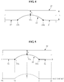
- FIGS. 5 and 6 are graphs illustrating a residual stress of an exemplary embodiment of a cover glass.
- FIG. 5 is a graph illustrating the first surface 31 of the cover glass 30 and a surface position of the groove 33
- FIG. 6 is a graph illustrating a residual stress at each surface position.
- a residual stress of a surface of the groove 33 is greater than a residual stress of the first surface 31.
- the cover glass 30 may have a residual stress in a range of about 1 MPa to about 10 MPa at the surface of the groove 33.
- the residual stress may be a stress that is generated inside a material which is processed or heat-treated, and the residual stress described herein may refer to a tensile stress or a compressive stress that is generated by thermal treatment, but exemplary embodiments are not limited thereto.
- the groove 33 of the cover glass 30 is defined through a thermal stripping process, which is to be described hereinbelow in regard to an exemplary embodiment of a method of manufacturing a display device, and a surface of the groove 33 may have a greater residual stress than that of the first surface 31.
- the groove 33 Since the groove 33 has a residual stress, the groove 33 of the cover glass 30 may experience significantly low mechanical strength degradation, even though it has a smaller thickness than that of the first surface 31. In addition, since having an arch shape, the groove 33 may experience significantly low strength degradation with respect to a pressure, even though it has a smaller thickness than that of the first surface 31.
- the minimum thickness t1 of the groove 33 may be reduced to about 5 % to about 30 % of the thickness t2 of the cover glass 30, and accordingly, sensitivity of the fingerprint recognition sensor 20 accommodated in the groove 33 may be improved.
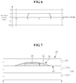
- FIG. 7 is a cross-sectional view taken along line II-II of FIG. 2
- FIG. 8 is a cross-sectional view illustrating an alternative exemplary embodiment of a display device.
- an exemplary embodiment of a display device may include a display panel 10, a fingerprint recognition sensor 20 on the display panel 10, and a cover glass 30 on the display panel 10 on which the fingerprint recognition sensor 20 is disposed.
- the cover glass 30 may be defined with a groove 33 on a first surface 31 which faces the display panel 10, in order to accommodate the fingerprint recognition sensor 20, and the fingerprint recognition sensor 20 accommodated in the groove 33 may be fixed to the cover glass 30 by an adhesive member 25.
- the adhesive member 25 may be an adhesive member including a transparent material.
- the adhesive member 25 may be an optically clear resin (OCR).
- an exemplary embodiment of a display device may include a display panel 10, a fingerprint recognition sensor 20 on the display panel 10, and a cover glass 30 on the display panel 10 on which the fingerprint recognition sensor 20 is disposed.
- the cover glass 30 may be defined with a groove 33 in a first surface 31 which faces the display panel 10, in order to accommodate the fingerprint recognition sensor 20.
- a high dielectric material 40 may further be disposed in the groove 33 of the cover glass 30.
- the high dielectric material 40 may include at least one (or any combination) selected from the group consisting of: low-melting glass (LMG), ZnO, Al 2 O 3 , Ta 2 O 5 , TiO 2 , ZrO 2 , La 2 O 3 , and Y 2 O 3 .
- LMG low-melting glass
- the LMG is a glass that further includes, for example, selenium, potassium, arsenic, and sulfur to achieve a melting point of about 130°C to about 350°C.
- the high dielectric material 40 may be formed on the groove 33 of the cover glass 30, having a thickness in a range of about 10 ⁇ m to about 100 ⁇ m.
- the high dielectric material 40 may be formed through a chemical vapor deposition process, a spin coating process, a sputtering process, a vacuum deposition process, and/or a printing process, for example.
- the fingerprint recognition sensor 20 accommodated in the groove 33 of the cover glass 30 in which the high dielectric material 40 is disposed may be fixed to the cover glass 30 by an adhesive member 25.
- the adhesive member 25 may be an adhesive member including a transparent material.
- the adhesive member 25 may be an optically clear resin (OCR).
- the groove 33 of the cover glass 30 may have a higher permittivity than a permittivity of the cover glass 30. Accordingly, a capacitance between the fingerprint recognition sensor 20 and a finger increases such that sensitivity of the fingerprint recognition sensor 20 may be improved.
- FIGS. 9A and 9B are views illustrating an exemplary embodiment of a method of manufacturing a display device.
- An exemplary embodiment of a method of manufacturing a display device may include defining an arch-shaped groove in a cover glass, accommodating a fingerprint recognition sensor in the groove of the cover glass, and coupling the cover glass and the display panel.
- defining of a groove 33 in a cover glass 30 may include contacting a heat source 50 to a first surface 31 of the cover glass 30, moving (i.e., transferring) the heat source 50 at a predetermined speed to chamfer the first surface 31 of the cover glass 30, and rapidly cooling the cover glass 30.
- the heat source 50 may have a temperature in a range of about 1200°C to about 1600°C, and may contact the cover glass 30 at a pressure in a range of about 100 kgf to about 500 kgf.
- the heat source 50 may be moved in various manners based on a planar shape, an area, and a depth of the groove 33.
- the cover glass 30 may experience a stripping phenomenon between a surface thereof and an inner portion thereof due to a difference between an expansive force and a contractile force. Such a stripping phenomenon may occur more readily as a coefficient of thermal expansion of the cover glass 30 increases.
- an exemplary embodiment of the groove 33 of the cover glass 30 may be defined using the thermal stripping phenomenon. Accordingly, the surface of the groove 33 may have characteristics of a relatively low surface roughness similar to a surface of a mirror. In addition, as the process is relatively simple, a manufacturing cost and a manufacturing time may be reduced.
- the groove 33 may have an arch-shaped cross-section, and by virtue of its structural characteristics, strength against a pressure may be improved and a residual stress, e.g., thermal stress, may remain such that mechanical strength may be improved.
- an arch-shaped groove is defined in a cover glass, and a fingerprint recognition sensor is accommodated therein, such that sensitivity of the fingerprint recognition sensor may be improved while strength degradation of the cover glass is significantly reduced.
- an arch-shaped groove is defined in a cover glass in a thermal stripping process such that a manufacturing process may be simplified and a manufacturing cost may be reduced.
Landscapes
- Engineering & Computer Science (AREA)
- Chemical & Material Sciences (AREA)
- Theoretical Computer Science (AREA)
- Physics & Mathematics (AREA)
- General Physics & Mathematics (AREA)
- Human Computer Interaction (AREA)
- Multimedia (AREA)
- Materials Engineering (AREA)
- Organic Chemistry (AREA)
- Life Sciences & Earth Sciences (AREA)
- Geochemistry & Mineralogy (AREA)
- General Chemical & Material Sciences (AREA)
- Chemical Kinetics & Catalysis (AREA)
- General Engineering & Computer Science (AREA)
- Computer Hardware Design (AREA)
- Devices For Indicating Variable Information By Combining Individual Elements (AREA)
- Image Input (AREA)
Abstract
Description
- This application claims priority from and the benefit of Korean Patent Application No.
10-2016-0072262, filed on June 10, 2016 - Exemplary embodiments relate to a display device and a method of manufacturing the display device, and more particularly, to a display device including a fingerprint recognition sensor and a method of manufacturing the display device.
- Recently, various functions have been applied to display devices in addition to an image representation function. For example, display devices may include a fingerprint recognition sensor.
- The fingerprint recognition sensors may be classified into a capacitive type, an optical type, a thermal type, and an ultrasonic type. Among the types of the fingerprint recognition sensors, the fingerprint recognition sensor of a capacitive type recognizes a fingerprint using a capacitance difference based on a distance between a ridge of the fingerprint and a valley of the fingerprint, which is sensed by finely disposed sensing electrodes.
- Sensitivity of the fingerprint recognition sensor may vary based on permittivity of a cover glass, thickness of the cover glass, or the like. In other words, as the permittivity of the cover glass increases and the thickness of the cover glass decreases, the sensitivity of the fingerprint recognition sensor may increase.
- However, there is a limitation in improving the sensitivity of the fingerprint recognition sensor due to material characteristics and strength degradation of the cover glass.
- The above information disclosed in this Background section is only for enhancement of understanding of the background of the inventive concept, and, therefore, it may contain information that does not form the prior art that is already known in this country to a person of ordinary skill in the art.
- Exemplary embodiments provide a display device capable of improving sensitivity of a fingerprint recognition sensor while effectively reducing strength degradation of a cover glass and to a method of manufacturing the display device.
- Additional aspects will be set forth in the detailed description which follows, and, in part, will be apparent from the disclosure, or may be learned by practice of the inventive concept.
- An exemplary embodiment discloses a display device that includes a display panel, a fingerprint recognition sensor on the display panel, and a cover glass on the fingerprint recognition sensor. The cover glass may be defined with at least one groove on a surface that faces the display panel.
- An exemplary embodiment discloses a method of manufacturing a display device that includes defining a groove in a cover glass, accommodating a fingerprint recognition sensor in the groove, and coupling the cover glass and the display panel. The defining of the groove in the cover glass includes contacting a heat source to a portion of the cover glass to be defined with the groove, moving the heat source at a predetermined speed to chamfer the cover glass, and cooling the cover glass rapidly.
- The foregoing general description and the following detailed description are exemplary and explanatory and are intended to provide further explanation of the claimed subject matter.
- The accompanying drawings, which are included to provide a further understanding of the inventive concept, and are incorporated in and constitute a part of this specification, illustrate exemplary embodiments of the inventive concept, and, together with the description, serve to explain principles of the inventive concept.
-
FIG. 1 is an exploded perspective view illustrating an exemplary embodiment of a display device. -
FIG. 2 is a plan view illustrating an exemplary embodiment of a display device. -
FIG. 3 is a plan view illustrating an alternative exemplary embodiment of a display device. -
FIG. 4 is a cross-sectional view taken along line I-I ofFIG. 1 . -
FIG. 5 andFIG. 6 are graphs illustrating residual stress of an exemplary embodiment of a cover glass. -
FIG. 7 is a cross-sectional view taken along line II-II ofFIG. 2 . -
FIG. 8 is a cross-sectional view illustrating an alternative exemplary embodiment of a display device. -
FIG. 9A and FIG. 9B are views illustrating an exemplary embodiment of a method of manufacturing a display device. - In the following description, for the purposes of explanation, numerous specific details are set forth in order to provide a thorough understanding of various exemplary embodiments. It is apparent, however, that various exemplary embodiments may be practiced without these specific details or with one or more equivalent arrangements. In other instances, well-known structures and devices are shown in block diagram form in order to avoid unnecessarily obscuring various exemplary embodiments.
- In the accompanying figures, the size and relative sizes of layers, films, panels, regions, etc., may be exaggerated for clarity and descriptive purposes. Also, like reference numerals denote like elements.
- When an element or layer is referred to as being "on," "connected to," or "coupled to" another element or layer, it may be directly on, connected to, or coupled to the other element or layer or intervening elements or layers may be present. When, however, an element or layer is referred to as being "directly on," "directly connected to," or "directly coupled to" another element or layer, there are no intervening elements or layers present. For the purposes of this disclosure, "at least one of X, Y, and Z" and "at least one selected from the group consisting of X, Y, and Z" may be construed as X only, Y only, Z only, or any combination of two or more of X, Y, and Z, such as, for instance, XYZ, XYY, YZ, and ZZ. Like numbers refer to like elements throughout. As used herein, the term "and/or" includes any and all combinations of one or more of the associated listed items.
- Although the terms first, second, etc. may be used herein to describe various elements, components, regions, layers, and/or sections, these elements, components, regions, layers, and/or sections should not be limited by these terms. These terms are used to distinguish one element, component, region, layer, and/or section from another element, component, region, layer, and/or section. Thus, a first element, component, region, layer, and/or section discussed below could be termed a second element, component, region, layer, and/or section without departing from the teachings of the present disclosure.
- Spatially relative terms, such as "beneath," "below," "lower," "above," "upper," and the like, may be used herein for descriptive purposes, and, thereby, to describe one element or feature's relationship to another element(s) or feature(s) as illustrated in the drawings. Spatially relative terms are intended to encompass different orientations of an apparatus in use, operation, and/or manufacture in addition to the orientation depicted in the drawings. For example, if the apparatus in the drawings is turned over, elements described as "below" or "beneath" other elements or features would then be oriented "above" the other elements or features. Thus, the exemplary term "below" can encompass both an orientation of above and below. Furthermore, the apparatus may be otherwise oriented (e.g., rotated 90 degrees or at other orientations), and, as such, the spatially relative descriptors used herein interpreted accordingly.
- The terminology used herein is for the purpose of describing particular embodiments and is not intended to be limiting. As used herein, the singular forms, "a," "an," and "the" are intended to include the plural forms as well, unless the context clearly indicates otherwise. Moreover, the terms "comprises," "comprising," "includes," and/or "including," when used in this specification, specify the presence of stated features, integers, steps, operations, elements, components, and/or groups thereof, but do not preclude the presence or addition of one or more other features, integers, steps, operations, elements, components, and/or groups thereof.
- Various exemplary embodiments are described herein with reference to sectional illustrations that are schematic illustrations of idealized exemplary embodiments and/or intermediate structures. As such, variations from the shapes of the illustrations as a result, for example, of manufacturing techniques and/or tolerances, are to be expected. Thus, exemplary embodiments disclosed herein should not be construed as limited to the particular illustrated shapes of regions, but are to include deviations in shapes that result from, for instance, manufacturing. As such, the regions illustrated in the drawings are schematic in nature and their shapes are not intended to illustrate the actual shape of a region of a device and are not intended to be limiting.
- Unless otherwise defined, all terms (including technical and scientific terms) used herein have the same meaning as commonly understood by one of ordinary skill in the art to which this disclosure is a part. Terms, such as those defined in commonly used dictionaries, should be interpreted as having a meaning that is consistent with their meaning in the context of the relevant art and will not be interpreted in an idealized or overly formal sense, unless expressly so defined herein. As used herein, "groove" refers to a cavity or indentation formed relative to a surface, as generally disclosed in the accompanying figures, and is not necessarily elongated, although it may be somewhat elongated.
-
FIG. 1 is an exploded perspective view illustrating an exemplary embodiment of a display device,FIG. 2 is a plan view illustrating an exemplary embodiment of a display device, andFIG. 3 is a plan view illustrating an alternative exemplary embodiment of a display device. - Referring to
FIG. 1 , an exemplary embodiment of a display device includes adisplay panel 10, afingerprint recognition sensor 20 on thedisplay panel 10, and acover glass 30 on thefingerprint recognition sensor 20. - The
display panel 10 may use any suitable panel, e.g., a liquid crystal display (LCD) panel, an organic light emitting diode (OLED) display panel, and a plasma display panel (PDP), which may display an image, without limitation. Hereinbelow, thedisplay panel 10 is described under the assumption that it is an LCD panel. - The
display panel 10 may include afirst substrate 111, asecond substrate 113 opposing thefirst substrate 111, and a liquid crystal layer (not illustrated) between thefirst substrate 111 and thesecond substrate 113. - The
display panel 10 may include a display area DA on which an image is displayed and a non-display area NDA around the display area DA. - The
fingerprint recognition sensor 20 may be disposed in the non-display area NDA of thedisplay panel 10. An exemplary embodiment of thefingerprint recognition sensor 20 is described under the assumption that it may be disposed in the non-display area NDA of thedisplay panel 10, but exemplary embodiments are not limited thereto. In an alternative exemplary embodiment, thefingerprint recognition sensor 20 may be disposed in the display area DA of thedisplay panel 10. - Any commonly used fingerprint recognition sensor may be applied to an exemplary embodiment of the present disclosure without limitation. The
fingerprint recognition sensor 20 may include a plurality of sensing electrodes arranged in a matrix form and a plurality of driving electrodes connected to the sensing electrodes. - The
cover glass 30 may be disposed over an entire surface of thedisplay panel 10 on which thefingerprint recognition sensor 20 is disposed. That is, thecover glass 30 may be disposed to cover the display area DA and the non-display area NDA of thedisplay panel 10. - The
cover glass 30 may include afirst surface 31 facing thedisplay panel 10 and asecond surface 32 which is an outer surface of the display device. Thefirst surface 31 of thecover glass 30 may be defined with an arch-shapedgroove 33 in which thefingerprint recognition sensor 20 is accommodated. - The
groove 33 is depicted inFIGS. 1 ,2 , and3 as having an elliptical shape on a plane, but exemplary embodiments are not limited thereto. Thegroove 33 may have any suitable shape or size on a plane based on the shape and size of thefingerprint recognition sensor 20. In other words, thegroove 33 may have various planar shapes such as a quadrangular shape, a circular shape, and an elliptical shape without departing from the inventive concept. - In addition, referring to
FIG. 2 , in a case where thefingerprint recognition sensor 20 is disposed in the non-display area NDA of thedisplay panel 10, thegroove 33 may be defined at a portion of thecover glass 30 corresponding to the non-display area NDA of thedisplay panel 10. - Similarly, referring to
FIG. 3 , in a case where thefingerprint recognition sensor 20 is disposed in the display area DA of thedisplay panel 10, thegroove 33 may be defined at a portion of thecover glass 30 corresponding to the display area DA of thedisplay panel 10. - In addition, although the
cover glass 30 defined with asingle groove 33 is depicted inFIGS. 2 and3 , exemplary embodiments are not limited thereto. In another exemplary embodiment, thecover glass 30 may be defined with at least onegroove 33. For example, thecover glass 30 may be defined with at least one groove in each of the display area DA and the non-display area NDA. That is, a groove may be defined in a predetermined portion of thecover glass 30. - The
cover glass 30 may be, for example, glass or sapphire, and it is assumed that an exemplary embodiment of thecover glass 30 is a glass of which a coefficient of thermal expansion (10-7/°C) is about 50 or higher. - In addition, although not illustrated in
FIG. 1 , a touch screen panel (not illustrated) may further be disposed between thedisplay panel 10 and thecover glass 30. The touch screen panel (not illustrated) may detect presence and location of a touch input. For example, a user may use the touch screen panel using a stylus pen (or a user's finger). The touch screen panel may include a transparent material. -
FIG. 4 is a cross-sectional view taken along line I-I ofFIG. 1 . - Referring to
FIG. 4 , an exemplary embodiment of thecover glass 30 includes thefirst surface 31 facing thedisplay panel 10 and thesecond surface 32 which may be an outer surface of the display device. Thefirst surface 31 may be defined with thegroove 33 in which the fingerprint recognition sensor or the like is accommodated. - However, exemplary embodiments are not limited thereto, and an alternative exemplary embodiment of the
cover glass 30 may be defined with an arch-shaped groove in thesecond surface 32. - A cross-section of the
groove 33 may have an arch shape. InFIG. 4 , thegroove 33 is depicted as having an arch shape which is symmetrical with respect to acentral portion 33a of thegroove 33, but exemplary embodiments are not limited thereto. In an alternative exemplary embodiment, thegroove 33 may have an arch shape which is non-symmetric with respect to thecentral portion 33a of thegroove 33. That is, the cross-section of thegroove 33 may be a curved surface. - In an exemplary embodiment, a thickness of the
cover glass 30 may decrease in a gradual manner from aportion 33b from which thegroove 33 begins toward thecentral portion 33a of thegroove 33. That is, thegroove 33 of thecover glass 30 may have a minimum thickness t1 at thecentral portion 33a. - The minimum thickness t1 may be about 5 % to about 95 % of a thickness t2 of the
cover glass 30. For example, the minimum thickness t1 may be about 5 % to about 30 % of the thickness t2 of thecover glass 30. - In an exemplary embodiment, the thickness t2 of the
cover glass 30 may be in a range of about 450 µm to about 550 µm, and the minimum thickness t1 of thegroove 33 may be in a range of about 150 µm to about 250 µm. -
FIGS. 5 and6 are graphs illustrating a residual stress of an exemplary embodiment of a cover glass. -
FIG. 5 is a graph illustrating thefirst surface 31 of thecover glass 30 and a surface position of thegroove 33, andFIG. 6 is a graph illustrating a residual stress at each surface position. - Referring to
FIGS. 5 and6 , in thecover glass 30, a residual stress of a surface of thegroove 33 is greater than a residual stress of thefirst surface 31. For example, thecover glass 30 may have a residual stress in a range of about 1 MPa to about 10 MPa at the surface of thegroove 33. - The residual stress may be a stress that is generated inside a material which is processed or heat-treated, and the residual stress described herein may refer to a tensile stress or a compressive stress that is generated by thermal treatment, but exemplary embodiments are not limited thereto.
- As an exemplary embodiment of the
groove 33 of thecover glass 30 is defined through a thermal stripping process, which is to be described hereinbelow in regard to an exemplary embodiment of a method of manufacturing a display device, and a surface of thegroove 33 may have a greater residual stress than that of thefirst surface 31. - Since the
groove 33 has a residual stress, thegroove 33 of thecover glass 30 may experience significantly low mechanical strength degradation, even though it has a smaller thickness than that of thefirst surface 31. In addition, since having an arch shape, thegroove 33 may experience significantly low strength degradation with respect to a pressure, even though it has a smaller thickness than that of thefirst surface 31. - Similarly, as mechanical strength degradation of the
groove 33 may be significantly reduced, the minimum thickness t1 of thegroove 33 may be reduced to about 5 % to about 30 % of the thickness t2 of thecover glass 30, and accordingly, sensitivity of thefingerprint recognition sensor 20 accommodated in thegroove 33 may be improved. -
FIG. 7 is a cross-sectional view taken along line II-II ofFIG. 2 , andFIG. 8 is a cross-sectional view illustrating an alternative exemplary embodiment of a display device. - Referring to
FIG. 7 , an exemplary embodiment of a display device may include adisplay panel 10, afingerprint recognition sensor 20 on thedisplay panel 10, and acover glass 30 on thedisplay panel 10 on which thefingerprint recognition sensor 20 is disposed. - The
cover glass 30 may be defined with agroove 33 on afirst surface 31 which faces thedisplay panel 10, in order to accommodate thefingerprint recognition sensor 20, and thefingerprint recognition sensor 20 accommodated in thegroove 33 may be fixed to thecover glass 30 by anadhesive member 25. - The
adhesive member 25 may be an adhesive member including a transparent material. For example, theadhesive member 25 may be an optically clear resin (OCR). - Referring to
FIG. 8 , an exemplary embodiment of a display device may include adisplay panel 10, afingerprint recognition sensor 20 on thedisplay panel 10, and acover glass 30 on thedisplay panel 10 on which thefingerprint recognition sensor 20 is disposed. - The
cover glass 30 may be defined with agroove 33 in afirst surface 31 which faces thedisplay panel 10, in order to accommodate thefingerprint recognition sensor 20. - In addition, a
high dielectric material 40 may further be disposed in thegroove 33 of thecover glass 30. - The
high dielectric material 40 may include at least one (or any combination) selected from the group consisting of: low-melting glass (LMG), ZnO, Al2O3, Ta2O5, TiO2, ZrO2, La2O3, and Y2O3. The LMG is a glass that further includes, for example, selenium, potassium, arsenic, and sulfur to achieve a melting point of about 130°C to about 350°C. - The
high dielectric material 40 may be formed on thegroove 33 of thecover glass 30, having a thickness in a range of about 10 µm to about 100 µm. Thehigh dielectric material 40 may be formed through a chemical vapor deposition process, a spin coating process, a sputtering process, a vacuum deposition process, and/or a printing process, for example. - The
fingerprint recognition sensor 20 accommodated in thegroove 33 of thecover glass 30 in which thehigh dielectric material 40 is disposed may be fixed to thecover glass 30 by anadhesive member 25. Theadhesive member 25 may be an adhesive member including a transparent material. For example, theadhesive member 25 may be an optically clear resin (OCR). - In an exemplary embodiment of a display device, as the
high dielectric material 40 is further disposed in thegroove 33 of thecover glass 30, thegroove 33 of thecover glass 30 may have a higher permittivity than a permittivity of thecover glass 30. Accordingly, a capacitance between thefingerprint recognition sensor 20 and a finger increases such that sensitivity of thefingerprint recognition sensor 20 may be improved. -
FIGS. 9A and 9B are views illustrating an exemplary embodiment of a method of manufacturing a display device. - An exemplary embodiment of a method of manufacturing a display device may include defining an arch-shaped groove in a cover glass, accommodating a fingerprint recognition sensor in the groove of the cover glass, and coupling the cover glass and the display panel.
- Referring to
FIGS. 9A and 9B , defining of agroove 33 in acover glass 30 may include contacting aheat source 50 to afirst surface 31 of thecover glass 30, moving (i.e., transferring) theheat source 50 at a predetermined speed to chamfer thefirst surface 31 of thecover glass 30, and rapidly cooling thecover glass 30. - In an exemplary embodiment, the
heat source 50 may have a temperature in a range of about 1200°C to about 1600°C, and may contact thecover glass 30 at a pressure in a range of about 100 kgf to about 500 kgf. - The
heat source 50 may be moved in various manners based on a planar shape, an area, and a depth of thegroove 33. - In a case where the
cover glass 30 is heated to a high temperature and then rapidly cooled, thecover glass 30 may experience a stripping phenomenon between a surface thereof and an inner portion thereof due to a difference between an expansive force and a contractile force. Such a stripping phenomenon may occur more readily as a coefficient of thermal expansion of thecover glass 30 increases. - As such, an exemplary embodiment of the
groove 33 of thecover glass 30 may be defined using the thermal stripping phenomenon. Accordingly, the surface of thegroove 33 may have characteristics of a relatively low surface roughness similar to a surface of a mirror. In addition, as the process is relatively simple, a manufacturing cost and a manufacturing time may be reduced. - In addition, due to characteristics of the thermal stripping, the
groove 33 may have an arch-shaped cross-section, and by virtue of its structural characteristics, strength against a pressure may be improved and a residual stress, e.g., thermal stress, may remain such that mechanical strength may be improved. - As such, in one or more exemplary embodiments of a display device, an arch-shaped groove is defined in a cover glass, and a fingerprint recognition sensor is accommodated therein, such that sensitivity of the fingerprint recognition sensor may be improved while strength degradation of the cover glass is significantly reduced.
- In addition, in one or more exemplary embodiments of a method of manufacturing the display device, an arch-shaped groove is defined in a cover glass in a thermal stripping process such that a manufacturing process may be simplified and a manufacturing cost may be reduced.
- Although certain exemplary embodiments and implementations have been described herein, other embodiments and modifications will be apparent from this description. Accordingly, the inventive concept is not limited to such embodiments, but rather to the broader scope of the presented claims and various obvious modifications and equivalent arrangements.
Claims (25)
- A display device, comprising:a display panel;a fingerprint recognition sensor on the display panel; anda cover glass on the fingerprint recognition sensor,wherein the cover glass is defined with at least one groove on a surface that faces the display panel.
- The display device of claim 1, wherein the fingerprint recognition sensor is accommodated in the groove.
- The display device of claim 1, wherein the groove has an arch-shaped cross-section.
- The display device of claim 1, wherein the cover glass has a greater residual stress within the groove than the cover glass outside the groove.
- The display device of claim 4, wherein the groove of the cover glass has a residual stress in a range of 1 MPa to 10 MPa.
- The display device of claim 1, wherein the cover glass has a minimum thickness at a central portion of the groove, and the minimum thickness is from 5 percent (%) to 95 % of a thickness of the cover glass.
- The display device of claim 6, wherein the minimum thickness is from 5 % to 30 % of the thickness of the cover glass.
- The display device of claim 2, further comprising an adhesive member between the groove and the fingerprint recognition sensor.
- The display device of claim 8, further comprising a high dielectric material between the groove and the adhesive member.
- The display device of claim 9, wherein the high dielectric material comprises at least one material selected from the group consisting of low melting glass (LMG), ZnO, Al2O3, Ta2O5, TiO2, ZrO2, La2O3, and Y2O3.
- The display device of claim 9, wherein the high dielectric material has a thickness in a range of 10 µm to 100 µm.
- The display device of claim 9, wherein the high dielectric material is LMG comprising material selected from the group consisting of selenium, potassium, arsenic, and sulfur.
- A method of manufacturing a display device, the method comprising:defining a groove in a cover glass;accommodating a fingerprint recognition sensor in the groove; andcoupling the cover glass and a display panel,wherein the defining of the groove in the cover glass comprises:contacting a heat source with a portion of the cover glass to be defined with the groove;moving the heat source at a predetermined speed to chamfer the cover glass; andcooling the cover glass rapidly.
- The method of claim 13, wherein the cover glass has a greater residual stress within the groove than the cover glass outside the groove.
- The method of claim 14, wherein the groove of the cover glass has a residual stress in a range of 1 Mpa to 10 Mpa.
- The method of claim 13, wherein the cover glass has a minimum thickness at a central portion of the groove, and the minimum thickness is in a range from 5 % to 95 % of a thickness of the cover glass.
- The method of claim 16, wherein the minimum thickness is in a range from 5 % to 30 % of the thickness of the cover glass.
- The method of claim 13, wherein the heat source has a temperature in a range from 1200°C to 1600°C.
- The method of claim 13, wherein the heat source contacts the cover glass at a pressure in a range from 100 kgf to 500 kgf.
- The method of claim 13, wherein the defining of the groove in the cover glass further comprises disposing a high dielectric material in the groove.
- The method of claim 13, wherein the groove has an arch-shaped cross-section.
- The method of claim 20, wherein the high dielectric material is selected from the group consisting of low melting glass (LMG), ZnO, Al2O3, Ta2O5, TiO2, ZrO2, La2O3, and Y2O3.
- The method of claim 20, wherein the high dielectric material is LMG comprising material selected from the group consisting of selenium, potassium, arsenic, and sulfur.
- The method of claim 20, wherein the high dielectric material is disposed in the groove to a thickness in a range of 10 µm to 100 µm.
- The method of claim 20, wherein the fingerprint recognition sensor is accommodated in the groove with an adhesive member.
Applications Claiming Priority (1)
| Application Number | Priority Date | Filing Date | Title |
|---|---|---|---|
| KR1020160072262A KR102709031B1 (en) | 2016-06-10 | 2016-06-10 | Display device and mufacturing method thereof |
Publications (2)
| Publication Number | Publication Date |
|---|---|
| EP3255584A2 true EP3255584A2 (en) | 2017-12-13 |
| EP3255584A3 EP3255584A3 (en) | 2018-04-18 |
Family
ID=59239763
Family Applications (1)
| Application Number | Title | Priority Date | Filing Date |
|---|---|---|---|
| EP17174665.4A Withdrawn EP3255584A3 (en) | 2016-06-10 | 2017-06-07 | Display device and manufacturing method thereof |
Country Status (4)
| Country | Link |
|---|---|
| US (1) | US10318789B2 (en) |
| EP (1) | EP3255584A3 (en) |
| KR (1) | KR102709031B1 (en) |
| CN (1) | CN107491143A (en) |
Cited By (1)
| Publication number | Priority date | Publication date | Assignee | Title |
|---|---|---|---|---|
| CN118729359A (en) * | 2024-08-30 | 2024-10-01 | 杭州老板电器股份有限公司 | An operation panel assembly and a fume treatment device |
Families Citing this family (14)
| Publication number | Priority date | Publication date | Assignee | Title |
|---|---|---|---|---|
| US10387707B2 (en) * | 2016-06-24 | 2019-08-20 | Idex Asa | Reinforcement panel for fingerprint sensor cover |
| KR102013053B1 (en) * | 2016-09-29 | 2019-08-21 | 선전 구딕스 테크놀로지 컴퍼니, 리미티드 | Screen assembly with a fingerprint module and electronic device |
| CN108254957A (en) * | 2018-01-05 | 2018-07-06 | 京东方科技集团股份有限公司 | Display base plate and preparation method thereof, display device |
| WO2019203575A1 (en) * | 2018-04-17 | 2019-10-24 | Samsung Electronics Co., Ltd. | Electronic device including multiple fixing members to fix biometric sensor to display and method for manufacturing the same |
| KR102495654B1 (en) * | 2018-04-17 | 2023-02-06 | 삼성전자주식회사 | Electronic device including a fingerprint sensor and manufactureing method thereof |
| KR102555513B1 (en) * | 2018-08-17 | 2023-07-17 | 삼성디스플레이 주식회사 | Electronic apparatus |
| CN111666781B (en) * | 2019-03-05 | 2024-05-10 | 京东方科技集团股份有限公司 | Display panel, manufacturing method thereof and display device |
| CN109785756B (en) * | 2019-03-15 | 2022-07-05 | 昆山国显光电有限公司 | Display panel and display device |
| KR102617248B1 (en) | 2019-03-19 | 2023-12-27 | 삼성디스플레이 주식회사 | Electronic apparatus |
| CN113366559A (en) * | 2019-07-10 | 2021-09-07 | 深圳市柔宇科技股份有限公司 | Flexible display device and electronic equipment |
| US11625945B2 (en) * | 2020-06-23 | 2023-04-11 | Synaptics Incorporated | Fingerprint sensor housing with non-uniform thickness |
| CN112286396A (en) * | 2020-11-02 | 2021-01-29 | 武汉华星光电技术有限公司 | Under-screen fingerprint display panel and under-screen fingerprint identification method |
| KR102921026B1 (en) | 2021-03-31 | 2026-02-02 | 삼성디스플레이 주식회사 | Display device and method for fabricating the same |
| KR20230132646A (en) * | 2022-03-08 | 2023-09-18 | 삼성디스플레이 주식회사 | Manufacturing method of electornic device |
Family Cites Families (22)
| Publication number | Priority date | Publication date | Assignee | Title |
|---|---|---|---|---|
| JP3965902B2 (en) | 2000-05-23 | 2007-08-29 | 株式会社日立製作所 | Manufacturing method of liquid crystal display device |
| JP4557606B2 (en) * | 2004-06-01 | 2010-10-06 | 日本板硝子株式会社 | Folded glass plate |
| US9158958B2 (en) | 2010-10-28 | 2015-10-13 | Synaptics Incorporated | Signal strength enhancement in a biometric sensor array |
| TWI469938B (en) | 2011-02-17 | 2015-01-21 | Mitsuboshi Diamond Ind Co Ltd | Scribing method of glass substrate |
| US8635887B2 (en) | 2011-08-10 | 2014-01-28 | Corning Incorporated | Methods for separating glass substrate sheets by laser-formed grooves |
| US10043052B2 (en) * | 2011-10-27 | 2018-08-07 | Synaptics Incorporated | Electronic device packages and methods |
| KR101405442B1 (en) | 2012-08-01 | 2014-06-13 | 주식회사 라미넥스 | Method for cutting of corner of glass using |
| KR20150057622A (en) | 2013-11-20 | 2015-05-28 | 주식회사 코디에스 | Device and method for processing substrate |
| CN104049803B (en) * | 2014-06-16 | 2017-03-29 | 深圳市汇顶科技股份有限公司 | a mobile terminal |
| CN105468187A (en) | 2014-06-18 | 2016-04-06 | 宸鸿科技(厦门)有限公司 | Touch panel with fingerprint recognition function |
| KR102220783B1 (en) | 2014-10-10 | 2021-02-26 | 엘지디스플레이 주식회사 | Display device including fingerprinting device and driving method the same |
| US9898644B2 (en) * | 2014-11-20 | 2018-02-20 | Chih-Chung Lin | Touch panel with fingerprint identification function |
| CN208044621U (en) * | 2014-12-11 | 2018-11-02 | 韩国科泰高科株式会社 | Electronic device cover window integrated fingerprint sensor module assembly |
| WO2016122173A1 (en) * | 2015-01-27 | 2016-08-04 | 엘지이노텍 주식회사 | Touch window |
| CN105844208A (en) * | 2015-01-30 | 2016-08-10 | 旭硝子株式会社 | Cover member, personal digital assistant and display device including the same, and method of manufacturing cover glass |
| TWI576734B (en) * | 2015-02-03 | 2017-04-01 | 宸鴻科技(廈門)有限公司 | Touch control device |
| CN104834892B (en) | 2015-03-06 | 2019-03-12 | 南昌欧菲生物识别技术有限公司 | Fingerprint identification device, touch screen and terminal equipment |
| CN104794454A (en) * | 2015-04-30 | 2015-07-22 | 京东方科技集团股份有限公司 | Fingerprint recognition device, display screen and display device |
| CN205384625U (en) * | 2015-06-05 | 2016-07-13 | 旭硝子株式会社 | Glass substrate , protection glass and key fob |
| CN204791061U (en) * | 2015-07-14 | 2015-11-18 | 阿里巴巴集团控股有限公司 | Terminal |
| CN105094234A (en) * | 2015-08-21 | 2015-11-25 | 广东欧珀移动通信有限公司 | Terminal |
| CN107451513B (en) * | 2016-05-31 | 2023-12-29 | 宸鸿科技(厦门)有限公司 | Fingerprint identification device |
-
2016
- 2016-06-10 KR KR1020160072262A patent/KR102709031B1/en active Active
-
2017
- 2017-03-31 US US15/475,989 patent/US10318789B2/en active Active
- 2017-06-07 EP EP17174665.4A patent/EP3255584A3/en not_active Withdrawn
- 2017-06-09 CN CN201710429980.0A patent/CN107491143A/en active Pending
Non-Patent Citations (1)
| Title |
|---|
| None |
Cited By (1)
| Publication number | Priority date | Publication date | Assignee | Title |
|---|---|---|---|---|
| CN118729359A (en) * | 2024-08-30 | 2024-10-01 | 杭州老板电器股份有限公司 | An operation panel assembly and a fume treatment device |
Also Published As
| Publication number | Publication date |
|---|---|
| EP3255584A3 (en) | 2018-04-18 |
| US10318789B2 (en) | 2019-06-11 |
| KR20170140454A (en) | 2017-12-21 |
| US20170357842A1 (en) | 2017-12-14 |
| KR102709031B1 (en) | 2024-09-24 |
| CN107491143A (en) | 2017-12-19 |
Similar Documents
| Publication | Publication Date | Title |
|---|---|---|
| US10318789B2 (en) | Display device and manufacturing method thereof | |
| KR101996437B1 (en) | Transparent protection window, flexible display apparatus with the same and the method for manufacturing the transparent protection window | |
| EP3979228A1 (en) | Flexible display cover plate, flexible display module and flexible display device | |
| CN104412206B (en) | Touch panel glass film layered product, touch panel and the touch panel manufacture method of glass film layered product | |
| US10466819B2 (en) | Flexible display device | |
| US20130149434A1 (en) | Method of cutting tempered glass and method of fabricating touchscreen using the same | |
| TW201902699A (en) | Flexible laminate comprising anisotropic layers | |
| US9063628B2 (en) | Capacitance-type touch sensor and display device equipped therewith | |
| EP3144782B1 (en) | Cover window for touch screen panel formed with printing layer and method for forming printing layer on cover window for touch screen panel | |
| US10963052B2 (en) | Touch sensitive element and display device comprising the same | |
| CN107003746A (en) | Input equipment, sensor, keyboard and electronic equipment | |
| KR20180012913A (en) | Window for display device and flexible display device including the same | |
| CN105700731A (en) | Touch sensor device and display device including the same | |
| US7259804B2 (en) | Method for fabricating touch panel integrated liquid crystal display device | |
| KR20110112203A (en) | Membrane Structures Having Inorganic Surface Structures and Related Manufacturing Methods | |
| WO2017087210A1 (en) | Touch screen panel with surface having rough feel | |
| KR20110108528A (en) | Capacitive touch panel having a transparent conductive film deposited directly on the cover layer and a manufacturing method thereof | |
| TWM522415U (en) | Touch display panel | |
| KR102658713B1 (en) | Force touch sensor | |
| KR102089637B1 (en) | Transparent electrical conductive film comprising metal nano wire and manufacturing method thereof | |
| CN117677088A (en) | Electronic device and manufacturing method thereof | |
| KR20160106314A (en) | Method of fabricating the substrate | |
| KR20160059869A (en) | Conductive film for touch screen | |
| KR20110038969A (en) | Touch panel-like member, manufacturing method thereof, and touch panel using planar member for touch panel | |
| CN106855766A (en) | Transparent electrode plate and its manufacture method |
Legal Events
| Date | Code | Title | Description |
|---|---|---|---|
| PUAI | Public reference made under article 153(3) epc to a published international application that has entered the european phase |
Free format text: ORIGINAL CODE: 0009012 |
|
| STAA | Information on the status of an ep patent application or granted ep patent |
Free format text: STATUS: THE APPLICATION HAS BEEN PUBLISHED |
|
| AK | Designated contracting states |
Kind code of ref document: A2 Designated state(s): AL AT BE BG CH CY CZ DE DK EE ES FI FR GB GR HR HU IE IS IT LI LT LU LV MC MK MT NL NO PL PT RO RS SE SI SK SM TR |
|
| AX | Request for extension of the european patent |
Extension state: BA ME |
|
| PUAL | Search report despatched |
Free format text: ORIGINAL CODE: 0009013 |
|
| AK | Designated contracting states |
Kind code of ref document: A3 Designated state(s): AL AT BE BG CH CY CZ DE DK EE ES FI FR GB GR HR HU IE IS IT LI LT LU LV MC MK MT NL NO PL PT RO RS SE SI SK SM TR |
|
| AX | Request for extension of the european patent |
Extension state: BA ME |
|
| RIC1 | Information provided on ipc code assigned before grant |
Ipc: G06F 3/044 20060101ALI20180314BHEP Ipc: G06K 9/00 20060101AFI20180314BHEP Ipc: C03C 17/23 20060101ALI20180314BHEP Ipc: C03C 15/00 20060101ALI20180314BHEP Ipc: C03C 17/02 20060101ALI20180314BHEP |
|
| STAA | Information on the status of an ep patent application or granted ep patent |
Free format text: STATUS: REQUEST FOR EXAMINATION WAS MADE |
|
| 17P | Request for examination filed |
Effective date: 20181018 |
|
| RBV | Designated contracting states (corrected) |
Designated state(s): AL AT BE BG CH CY CZ DE DK EE ES FI FR GB GR HR HU IE IS IT LI LT LU LV MC MK MT NL NO PL PT RO RS SE SI SK SM TR |
|
| STAA | Information on the status of an ep patent application or granted ep patent |
Free format text: STATUS: THE APPLICATION HAS BEEN WITHDRAWN |
|
| 18W | Application withdrawn |
Effective date: 20190704 |