EP3253177A1 - Double-sided thick film heating element having high thermal conductivity - Google Patents
Double-sided thick film heating element having high thermal conductivity Download PDFInfo
- Publication number
- EP3253177A1 EP3253177A1 EP16883017.2A EP16883017A EP3253177A1 EP 3253177 A1 EP3253177 A1 EP 3253177A1 EP 16883017 A EP16883017 A EP 16883017A EP 3253177 A1 EP3253177 A1 EP 3253177A1
- Authority
- EP
- European Patent Office
- Prior art keywords
- thick film
- carrier
- covering layer
- film coating
- heating
- Prior art date
- Legal status (The legal status is an assumption and is not a legal conclusion. Google has not performed a legal analysis and makes no representation as to the accuracy of the status listed.)
- Granted
Links
Classifications
-
- H—ELECTRICITY
- H05—ELECTRIC TECHNIQUES NOT OTHERWISE PROVIDED FOR
- H05B—ELECTRIC HEATING; ELECTRIC LIGHT SOURCES NOT OTHERWISE PROVIDED FOR; CIRCUIT ARRANGEMENTS FOR ELECTRIC LIGHT SOURCES, IN GENERAL
- H05B3/00—Ohmic-resistance heating
- H05B3/10—Heating elements characterised by the composition or nature of the materials or by the arrangement of the conductor
- H05B3/12—Heating elements characterised by the composition or nature of the materials or by the arrangement of the conductor characterised by the composition or nature of the conductive material
-
- H—ELECTRICITY
- H05—ELECTRIC TECHNIQUES NOT OTHERWISE PROVIDED FOR
- H05B—ELECTRIC HEATING; ELECTRIC LIGHT SOURCES NOT OTHERWISE PROVIDED FOR; CIRCUIT ARRANGEMENTS FOR ELECTRIC LIGHT SOURCES, IN GENERAL
- H05B3/00—Ohmic-resistance heating
- H05B3/10—Heating elements characterised by the composition or nature of the materials or by the arrangement of the conductor
- H05B3/18—Heating elements characterised by the composition or nature of the materials or by the arrangement of the conductor the conductor being embedded in an insulating material
-
- H—ELECTRICITY
- H05—ELECTRIC TECHNIQUES NOT OTHERWISE PROVIDED FOR
- H05B—ELECTRIC HEATING; ELECTRIC LIGHT SOURCES NOT OTHERWISE PROVIDED FOR; CIRCUIT ARRANGEMENTS FOR ELECTRIC LIGHT SOURCES, IN GENERAL
- H05B3/00—Ohmic-resistance heating
- H05B3/20—Heating elements having extended surface area substantially in a two-dimensional [2D] plane, e.g. plate-heater
- H05B3/22—Heating elements having extended surface area substantially in a two-dimensional [2D] plane, e.g. plate-heater non-flexible
- H05B3/26—Heating elements having extended surface area substantially in a two-dimensional [2D] plane, e.g. plate-heater non-flexible heating conductor mounted on insulating base
- H05B3/265—Heating elements having extended surface area substantially in a two-dimensional [2D] plane, e.g. plate-heater non-flexible heating conductor mounted on insulating base the insulating base being an inorganic material, e.g. ceramic
-
- H—ELECTRICITY
- H05—ELECTRIC TECHNIQUES NOT OTHERWISE PROVIDED FOR
- H05B—ELECTRIC HEATING; ELECTRIC LIGHT SOURCES NOT OTHERWISE PROVIDED FOR; CIRCUIT ARRANGEMENTS FOR ELECTRIC LIGHT SOURCES, IN GENERAL
- H05B3/00—Ohmic-resistance heating
- H05B3/02—Details
- H05B3/06—Heater elements structurally combined with coupling elements or holders
-
- H—ELECTRICITY
- H05—ELECTRIC TECHNIQUES NOT OTHERWISE PROVIDED FOR
- H05B—ELECTRIC HEATING; ELECTRIC LIGHT SOURCES NOT OTHERWISE PROVIDED FOR; CIRCUIT ARRANGEMENTS FOR ELECTRIC LIGHT SOURCES, IN GENERAL
- H05B3/00—Ohmic-resistance heating
- H05B3/10—Heating elements characterised by the composition or nature of the materials or by the arrangement of the conductor
- H05B3/16—Heating elements characterised by the composition or nature of the materials or by the arrangement of the conductor the conductor being mounted on an insulating base
-
- H—ELECTRICITY
- H05—ELECTRIC TECHNIQUES NOT OTHERWISE PROVIDED FOR
- H05B—ELECTRIC HEATING; ELECTRIC LIGHT SOURCES NOT OTHERWISE PROVIDED FOR; CIRCUIT ARRANGEMENTS FOR ELECTRIC LIGHT SOURCES, IN GENERAL
- H05B3/00—Ohmic-resistance heating
- H05B3/20—Heating elements having extended surface area substantially in a two-dimensional [2D] plane, e.g. plate-heater
- H05B3/22—Heating elements having extended surface area substantially in a two-dimensional [2D] plane, e.g. plate-heater non-flexible
- H05B3/26—Heating elements having extended surface area substantially in a two-dimensional [2D] plane, e.g. plate-heater non-flexible heating conductor mounted on insulating base
- H05B3/267—Heating elements having extended surface area substantially in a two-dimensional [2D] plane, e.g. plate-heater non-flexible heating conductor mounted on insulating base the insulating base being an organic material, e.g. plastic
-
- H—ELECTRICITY
- H05—ELECTRIC TECHNIQUES NOT OTHERWISE PROVIDED FOR
- H05B—ELECTRIC HEATING; ELECTRIC LIGHT SOURCES NOT OTHERWISE PROVIDED FOR; CIRCUIT ARRANGEMENTS FOR ELECTRIC LIGHT SOURCES, IN GENERAL
- H05B2203/00—Aspects relating to Ohmic resistive heating covered by group H05B3/00
- H05B2203/013—Heaters using resistive films or coatings
Definitions
- the present invention relates to the field of thick film, and more particularly to a thick film element with high heat conductivity on two sides thereof.
- Thick film heating elements refer to heating elements that are made by fabricating exothermic materials on a substrate thick films and providing electricity to generate heat.
- the conventional heating methods include electrical heating tube heating and PTC heating.
- An electrical heated tube heating element uses a metal tube as the outer case and distributes spirally nickel-chromium or iron-chromium alloy spirally therein to form heater strips; the clearance space is then filled with magnesite clinker that has excellent thermal conductivity and insulativity and sealed with silica gel from two ends of the tube.
- the PTC heating method uses ceramics as the exothermic material. Both electrical heated tube heating and PTC heating conduct heating indirectly with low thermal efficiency, and are structurally huge and bulky. Besides, in consideration of environmental protection, heaters using these two types of heating methods stain easily after repeatedly heating and cleaning thereof is not easy. Additionally, PTC heaters contain lead and other hazardous substances and are easily oxidized, causing power attenuation and short service life.
- Chinese application CN201210320614.9 discloses an aluminum alloy heating tube using thick film heating, which comprises a heating tube body and a thick film heating plate.
- An insertion slot the depth direction of which extends radially inward, is disposed at a side of the heating tube body.
- the thick film heating plate is positioned in the insertion slot.
- the heating tube body has through-holes, the length direction of which extend axially inward along the heating tube body, disposed on two sides of the insertion slot.
- the thick film heating circuit on the thick film circuit board is printed on the ceramics substrate or a substrate of other insulating material.
- the thick film circuit board is coated with one more layer of insulating medium; therefore, the surface of the entire thick film circuit board is insulative.
- Chinese application CN201010110037.1 discloses a thick film heating assembly with dry burning protection function, which comprises a thick film heater for electrical heating, an electrical connection bracket mounted on the thick film heater for connecting the thick film heater with external components, and a dry-burning protector mounted on the thick film heater.
- the electrical connection bracket and the dry-burning protector form the whole components, and the dry-burning protector contains at least one electrical dry-burning-proof protector electrically connected to the control circuit and one mechanical dry-burning-proof protector.
- the existing heating elements have gradually been applied to the field of household electrical appliances, the heating bodies of the thick film element mentioned above are attached onto the electrical appliances, and few independent components are existed at present. Up to date, none of the existing heating elements has double-sided high heat conductivity, and no double-sided heating thick film element has been applied to daily living and industrial production to realize the function of uniform heating on both sides of the element.
- the present invention provides a thick film element with high heat conductivity on two sides thereof with the advantages of small volume, high efficiency, environmental-friendly, high safety performance and long service lifespan.
- Thick film is a film layer with a thickness ranging from several microns to tens of microns formed by printing and sintering on a carrier; the material used to manufacture the film layer is known as thick film material, and the coating made from the thick film is called thick film coating.
- the thick film heating element has the advantages of high power density, fast heating speed, high working temperature, fast heat generating rate, high mechanical strength, small volume, easy installation, uniform heating temperature field, long lifespan, energy saving and environmental friendly, and excellent safety performance.
- the thick film element with high heat conductivity on two sides thereof of the present invention comprises a carrier, a thick film coating deposited on the carrier, and a covering layer overlaid on the coating.
- the thick film coating is a heating material, and the mode of heating is electrical heating.
- the covering layer is a dielectric layer coating on the thick film coating by printing or sintering, and the area of the covering layer is larger than that of the thick film coating.
- the carrier is the dielectric layer carrying the thick film coating.
- the thick film coating covers the carrier by printing or sintering.
- the heat conductivity coefficient refers to the heat transferred by a one-meter thick material having a temperature difference between two side surfaces of 1 degree (K, °C), through one square meter (1 m 2 ) area within one second (IS) under a stable heat transfer condition.
- Unit of the heat conductivity coefficient is watt/meter ⁇ degree (W/(m ⁇ K), and K may be replaced by °C).
- the covering layer, the thick film coating and carrier sticks closely with each other at the electrical heating parts of the thick film heating elements, and both ends of the thick film coating connect to external electrodes.
- the present invention features in that both sides of the thick film element have high heat conductivity, and that the heat generating rate of the covering layer, the thick film coating and the carrier should meet the following requirements:
- the heat transfer rates of the covering layer and the carrier are determined by the properties of the material and the thick film heating element.
- the carrier and the thick film coating are bound by printing or sintering
- the thick film coating and the covering layer are bound by printing or sintering.
- the region between the carrier and the covering layer without the thick film coating is bound by printing or sintering.
- the carrier includes polyimides, organic insulating materials, inorganic insulating materials, ceramics, glass ceramics, quartz, crystal and stone materials.
- the thick film coating is one or more of silver, platinum, palladium, palladium oxide, gold or rare earth materials.
- the covering layer is made from one or more of polyester, polyimide or polyetherimide (PEI), ceramics, silica gel, asbestos, micarex.
- PET polyimide or polyetherimide
- the area of the thick film coating is smaller than or equal to that of the covering layer or the carrier.
- the present invention also provides a use of the thick film elements for products with double-sided heating.
- the present invention discloses a thick film element with high heat conductivity on two sides thereof of the present invention, comprises a carrier, a thick film coating deposited on the carrier, and a covering layer overlaid on the coating.
- the thick film coating is a heating material, and the mode of heating is electrical heating.
- the following embodiments include 20 thick film elements prepared by the applicant, and the materials for preparing the covering layer, the thick film coating and the carrier of the 20 listed thick film elements all satisfy the above equations above.
- the detailed preparing method and formula are provided as follows:
- Silver paste with a heat conductivity coefficient of ⁇ 2 is selected to prepare the thick film coating
- polyimides with a heat conductivity coefficient of ⁇ 3 is selected to prepare the carrier
- polyimides with a heat conductivity coefficient of ⁇ 1 is selected to prepare the covering layer.
- the three layers are bound by sintering.
- the area of the prepared thick film coating is A 2 , the thickness is b 2 ; the area of the covering layer is A 1 , the thickness is b 1 ; the area of the carrier is A 3 , the thickness is b 3 .
- the thick film starts to heat up; when the heating is stabled, measure the surface temperature of the covering layer and the carrier, and the heating temperature of the thick film coating under a stable heating state is measured.
- Tables 1 to 4 are the 20 thick film elements prepared by the applicant. After provided electricity to heat for 2 minutes, the thick film elements are measured according to the national standards to obtain the performance data (heat conductivity coefficient, surface temperature) as shown in the Tables. The thickness, contact area, initial temperature are measured before heating.
- Table 1 is the performance data of the covering layers of the thick film elements in Embodiments 1 to 20. The details are as follows: Table 1 Covering Layer Heat Conductivity Coefficient ⁇ 1 (W/m.k) Thickness b 1 ( ⁇ m) Surface Temperature T 1 (°C) T Minimum melting point of the covering laye r (°C) Initial Temperature T 0 (°C) Embodiment 1 7.2 25 113 350 25 Embodiment 2 7.2 25 55 350 25 Embodiment 3 7.2 25 102 350 25 Embodiment 4 7.2 50 53 350 25 Embodiment 5 7.2 50 97 350 25 Embodiment 6 7.2 75 51 350 25 Embodiment 7 7.2 75 94 350 25 Embodiment 8 7.2 75 47 350 25 Embodiment 9 7.2 100 93 350 25 Embodiment 10 7.2 100 44 350 25 Embodiment 11 7.2 200 48 350 25 Embodiment 12 7.2 200 93 350 25 Embodiment 13 7.2 300 91 350 25 Embodiment 14 7.2 300 44 350
- Table 2 is the performance data of the thick film coatings of the thick film elements in Embodiments 1 to 20. The details are as follows: Table 2 Thick Film Coating Heat Conductivity Coefficient ⁇ 2 (W/m.k) Thickness b 2 ( ⁇ m) Area A 2 (m 2 ) Heating temperature T 2 (°C) Initial temperature T 0 (°C) Embodiment 1 382 50 0.016 116 25 Embodiment 2 382 50 0.056 56 25 Embodiment 3 382 40 0.016 103 25 Embodiment 4 382 40 0.056 54 25 Embodiment 5 382 30 0.016 98 25 Embodiment 6 382 30 0.056 52 25 Embodiment 7 382 30 0.016 95 25 Embodiment 8 382 25 0.056 51 25 Embodiment 9 382 25 0.016 97 25 Embodiment 10 382 25 0.056 46 25 Embodiment 11 382 30 0.016 49 25 Embodiment 12 382 30 0.056 95 25 Embodiment 13
- Table 3 is the performance data of the carriers of the thick film elements in Embodiments 1 to 20. The details are as follows: Table 3 Carrier Heat Conductivity Coefficient ⁇ 3 (W/m.k) Thickness b 3 ( ⁇ m) Surface Temperature T 3 (°C) T Minimum melting point of the carrier (°C) Initial Temperature T 0 (°C) Embodiment 1 7.2 1 105 350 25 Embodiment2 7.2 2 42 350 25 Embodiment 3 7.2 3 87 350 25 Embodiment4 7.2 1 43 350 25 Embodiment 5 7.2 2 86 350 25 Embodiment 6 7.2 1 40 350 25 Embodiment 7 7.2 2 84 350 25 Embodiment 8 7.2 3 38 350 25 Embodiment 9 7.2 1 87 350 25 Embodiment 10 7.2 2 40 350 25 Embodiment 11 7.2 3 38 350 25 Embodiment 12 7.2 4 78 350 25 Embodiment 13 7.2 1 85 350 25 Embodiment 14 7.2 2 39 350 25 Embodiment 15
- Table 4 is the heat transfer rate calculated according to the performance data listed in Tables 1, 2 and 3.
- Tables 5 to 8 are the performance data of the thick film elements in Contrasting Examples 1 to 3 of the present invention. All the performance data is measured as those shown in Tables 1 to 4. The details are as follows: Table 5 Covering Layer Heat Conductivity Coefficient ⁇ 1 (W/m.k) Thickness b 1 ( ⁇ m) Surface Temperature T 1 (°C) T Minimum melting point of the covering layer (°C) Initial Temperature T 0 (°C) Contrasting Example 1 7.2 25 102 350 25 Contrasting Example 2 7.2 50 97 350 25 Contrasting Example 3 7.2 75 94 350 25 Table 6 Thick Film Coating Heat Conductivity Coefficient ⁇ 2 (W/m.k) Thickness b 2 ( ⁇ m) Area A 2 (m 2 ) Heating Temperature T 2 (°C) Initial Temperature T 0 (°C) Contrasting Example 1 382 40 0.016 103 25 Contrasting Example 2 382 30 0.016 96 25 Contrasting Example 3 382 30 0.016 95 25 Table 7 Carrier Heat Conductivity Coefficient ⁇ 3 (W/m
- Contrasting Example 1 359424 11918400 1190.4 33.1 10012.09 301
- Contrasting Example 2 163584 14872533 648 90.9 22951.44 252
- Contrasting Example 3 107520 1421333.3 644 13 2207.03 166 No
Landscapes
- Chemical & Material Sciences (AREA)
- Engineering & Computer Science (AREA)
- Ceramic Engineering (AREA)
- Surface Heating Bodies (AREA)
- Resistance Heating (AREA)
- Fixing For Electrophotography (AREA)
- Laminated Bodies (AREA)
Abstract
Description
- The present invention relates to the field of thick film, and more particularly to a thick film element with high heat conductivity on two sides thereof.
- Thick film heating elements refer to heating elements that are made by fabricating exothermic materials on a substrate thick films and providing electricity to generate heat. The conventional heating methods include electrical heating tube heating and PTC heating. An electrical heated tube heating element uses a metal tube as the outer case and distributes spirally nickel-chromium or iron-chromium alloy spirally therein to form heater strips; the clearance space is then filled with magnesite clinker that has excellent thermal conductivity and insulativity and sealed with silica gel from two ends of the tube. The PTC heating method uses ceramics as the exothermic material. Both electrical heated tube heating and PTC heating conduct heating indirectly with low thermal efficiency, and are structurally huge and bulky. Besides, in consideration of environmental protection, heaters using these two types of heating methods stain easily after repeatedly heating and cleaning thereof is not easy. Additionally, PTC heaters contain lead and other hazardous substances and are easily oxidized, causing power attenuation and short service life.
- Chinese application
CN201210320614.9 - Chinese application
CN201010110037.1 - Although the existing heating elements have gradually been applied to the field of household electrical appliances, the heating bodies of the thick film element mentioned above are attached onto the electrical appliances, and few independent components are existed at present. Up to date, none of the existing heating elements has double-sided high heat conductivity, and no double-sided heating thick film element has been applied to daily living and industrial production to realize the function of uniform heating on both sides of the element.
- To solve these problems mentioned above, the present invention provides a thick film element with high heat conductivity on two sides thereof with the advantages of small volume, high efficiency, environmental-friendly, high safety performance and long service lifespan.
- The concept of thick film in the present invention is a term comparative to thin films. Thick film is a film layer with a thickness ranging from several microns to tens of microns formed by printing and sintering on a carrier; the material used to manufacture the film layer is known as thick film material, and the coating made from the thick film is called thick film coating. The thick film heating element has the advantages of high power density, fast heating speed, high working temperature, fast heat generating rate, high mechanical strength, small volume, easy installation, uniform heating temperature field, long lifespan, energy saving and environmental friendly, and excellent safety performance.
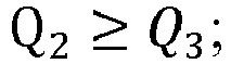
- The thick film element with high heat conductivity on two sides thereof of the present invention, comprises a carrier, a thick film coating deposited on the carrier, and a covering layer overlaid on the coating. The thick film coating is a heating material, and the mode of heating is electrical heating. The carrier, the thick film coating and the covering layer are selected from a material that fulfills every of the following equations:


A represents the contact area of the thick film coating with the covering layer or the carrier;
b1 represents the thickness of the covering layer; b2 represents the thickness of the thick film coating; b3 represents the thickness of the carrier;
T0 represents the initial temperature of the thick film heating element; T1 represents the surface temperature of the covering layer; T2 represents the heating temperature of the thick film coating; T3 represents the surface temperature of the carrier;


- The covering layer is a dielectric layer coating on the thick film coating by printing or sintering, and the area of the covering layer is larger than that of the thick film coating.
- The carrier is the dielectric layer carrying the thick film coating. The thick film coating covers the carrier by printing or sintering.
- The heat conductivity coefficient refers to the heat transferred by a one-meter thick material having a temperature difference between two side surfaces of 1 degree (K, °C), through one square meter (1 m2) area within one second (IS) under a stable heat transfer condition. Unit of the heat conductivity coefficient is watt/meter·degree (W/(m·K), and K may be replaced by °C).
- The covering layer, the thick film coating and carrier sticks closely with each other at the electrical heating parts of the thick film heating elements, and both ends of the thick film coating connect to external electrodes. When given electricity, the thick film coating is heated and becomes hot after electricity energy is transformed to thermal energy. Heat generating rate of the thick film coating could be calculated by Q 2 =

- The present invention features in that both sides of the thick film element have high heat conductivity, and that the heat generating rate of the covering layer, the thick film coating and the carrier should meet the following requirements:
- (1) The heat transfer rate of the covering layer and the thick film coating should satisfy the following formula: Q1=a×Q3, wherein 0.1≤a≤150; for those thick film elements satisfied the above equation, the covering layer and the carrier of the thick film heating element have a uniform heat transfer ability, thus avoiding overly fast temperature raising on one side and overly slow temperature raising on the other side of the thick film element and avoiding the phenomenon of uneven heating on the two sides, which would not meet the technical effect of the present invention;
- (2) The heat generating rate of the thick film coating and the heat transfer rate of the covering layer should satisfy the following formula: Q2 ≥ Q 1, and Q2 = b × Q1, wherein 1≤b≤2500; if the heat generating rate of the thick film coating is much larger than the heat transfer rate of the covering layer, the continuously accumulated heat of the thick film coating could not be conducted away, such that the temperature of the thick film coating keeps rising, and when the temperature is higher than the minimum melting point of the covering layer, the covering layer would begin to melt or even burn, which would destroy the structure of the covering layer or the carrier, thus destroying the thick film heating elements.
- (3) The heat generating rate of the thick film coating and the heat transfer rate of the carrier should satisfy the following formula: Q2 ≥ Q3, and Q2=c×Q3, 100≤c≤ 10000; if the heat generating rate of the thick film coating is much larger than the heat transfer rate of the carrier, the continuously accumulated heat of the thick film coating could not be conducted away, such that the temperature of the thick film coating keeps rising, and when the temperature is higher than the minimum melting point of the carrier, the carrier would begin to melt or even burn, which would destroy the structure of the carrier, thus destroying the thick film heating elements.
- (4) The heating temperature of the thick film coating could not be higher than the minimum melting point of the covering layer or the carrier, and should meet the requirements: T2 < TMinimum melting point of the covering layer and T2 < TMinimum melting point of the carrier. Excessively high heating temperature should be avoided to prevent destruction of the thick film heating elements.
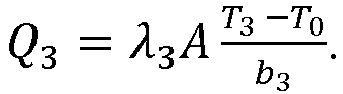
- When the above-mentioned requirements are met, the heat transfer rates of the covering layer and the carrier are determined by the properties of the material and the thick film heating element. The formula for calculating the heat transfer rate of the covering layer is

- The formula for calculating the heat transfer rate of the carrier is

- Preferably, the carrier and the thick film coating are bound by printing or sintering, the thick film coating and the covering layer are bound by printing or sintering.
- Preferably, the region between the carrier and the covering layer without the thick film coating is bound by printing or sintering.
- Preferably, the carrier includes polyimides, organic insulating materials, inorganic insulating materials, ceramics, glass ceramics, quartz, crystal and stone materials.
- Preferably, the thick film coating is one or more of silver, platinum, palladium, palladium oxide, gold or rare earth materials.
- Preferably, the covering layer is made from one or more of polyester, polyimide or polyetherimide (PEI), ceramics, silica gel, asbestos, micarex.
- Preferably, the area of the thick film coating is smaller than or equal to that of the covering layer or the carrier.
- The present invention also provides a use of the thick film elements for products with double-sided heating.
- The beneficial effects of the present invention are as follows:
- (1) The thick film element of the present invention has high heat conductivity and uniform heat generating rate on two sides thereof, and shows improved heat transfer efficiency.
- (2) The three-layered structure of the thick film element of the present invention could be bound directly by printing or sintering, and the thick film coating would heat the covering layer directly so as to improve the heat conduction efficiency. Additionally, the covering layer of the present invention covers the thick film coating, thus avoiding the problem of electric leakage when the thick film coating is given electricity and improving safety performance.
- (3) The thick film element of the present invention could be applied in products that require high heat conductivity on both sides, meeting the market demand for multifunctional heating products.
- (4) The thick film heating element of the present invention generates heat by the thick film coating. The thickness of the thick film coating is at the micrometer level, thus generating heat evenly after given electricity. The thick film element has a long service lifespan.
- The present invention will now be described more specifically with reference to the following embodiments. It is to be noted that the following descriptions of preferred embodiments of this invention are presented herein for purpose of illustration and description only. It is not intended to be exhaustive or to be limited to the precise form disclosed.
- The present invention discloses a thick film element with high heat conductivity on two sides thereof of the present invention, comprises a carrier, a thick film coating deposited on the carrier, and a covering layer overlaid on the coating. The thick film coating is a heating material, and the mode of heating is electrical heating. The carrier, the thick film coating and the covering layer are selected from a material that fulfills every of the following equations:


b1 represents the thickness of the covering layer; b3 represents the thickness of the carrier,

- The following embodiments include 20 thick film elements prepared by the applicant, and the materials for preparing the covering layer, the thick film coating and the carrier of the 20 listed thick film elements all satisfy the above equations above. The detailed preparing method and formula are provided as follows:
- Silver paste with a heat conductivity coefficient of λ2 is selected to prepare the thick film coating, polyimides with a heat conductivity coefficient of λ3 is selected to prepare the carrier, and polyimides with a heat conductivity coefficient of λ1 is selected to prepare the covering layer. The three layers are bound by sintering. The area of the prepared thick film coating is A2, the thickness is b2; the area of the covering layer is A1, the thickness is b1; the area of the carrier is A3, the thickness is b3.
- Turn on an external DC power supply to charge the thick film coating. The thick film starts to heat up; when the heating is stabled, measure the surface temperature of the covering layer and the carrier, and the heating temperature of the thick film coating under a stable heating state is measured. Heat transfer rate of the covering layer and the carrier, and heat generating rate of the thick film coating are calculated according to the following formula:


- Tables 1 to 4 are the 20 thick film elements prepared by the applicant. After provided electricity to heat for 2 minutes, the thick film elements are measured according to the national standards to obtain the performance data (heat conductivity coefficient, surface temperature) as shown in the Tables. The thickness, contact area, initial temperature are measured before heating.
- Table 1 is the performance data of the covering layers of the thick film elements in Embodiments 1 to 20. The details are as follows:
Table 1 Covering Layer Heat Conductivity Coefficient λ1 (W/m.k) Thickness b1 (µm) Surface Temperature T1 (°C) TMinimum melting point of the covering layer (°C) Initial Temperature T0 (°C) Embodiment 1 7.2 25 113 350 25 Embodiment 2 7.2 25 55 350 25 Embodiment 3 7.2 25 102 350 25 Embodiment 4 7.2 50 53 350 25 Embodiment 5 7.2 50 97 350 25 Embodiment 6 7.2 75 51 350 25 Embodiment 7 7.2 75 94 350 25 Embodiment 8 7.2 75 47 350 25 Embodiment 9 7.2 100 93 350 25 Embodiment 10 7.2 100 44 350 25 Embodiment 11 7.2 200 48 350 25 Embodiment 12 7.2 200 93 350 25 Embodiment 13 7.2 300 91 350 25 Embodiment 14 7.2 300 44 350 25 Embodiment 15 7.2 400 96 350 25 Embodiment 16 7.2 400 44 350 25 Embodiment 17 7.2 500 101 350 25 Embodiment 18 7.2 500 47 350 25 Embodiment 19 7.2 600 92 350 25 Embodiment 20 7.2 600 30 350 25 - Table 2 is the performance data of the thick film coatings of the thick film elements in Embodiments 1 to 20. The details are as follows:
Table 2 Thick Film Coating Heat Conductivity Coefficient λ2 (W/m.k) Thickness b2 (µm) Area A2 (m2) Heating temperature T2 (°C) Initial temperature T0 (°C) Embodiment 1 382 50 0.016 116 25 Embodiment 2 382 50 0.056 56 25 Embodiment 3 382 40 0.016 103 25 Embodiment 4 382 40 0.056 54 25 Embodiment 5 382 30 0.016 98 25 Embodiment 6 382 30 0.056 52 25 Embodiment 7 382 30 0.016 95 25 Embodiment 8 382 25 0.056 51 25 Embodiment 9 382 25 0.016 97 25 Embodiment 10 382 25 0.056 46 25 Embodiment 11 382 30 0.016 49 25 Embodiment 12 382 30 0.056 95 25 Embodiment 13 382 20 0.016 95 25 Embodiment 14 382 20 0.056 45 25 Embodiment 15 382 30 0.016 99 25 Embodiment 16 382 30 0.056 46 25 Embodiment 17 382 35 0.016 103 25 Embodiment 18 382 35 0.056 49 25 Embodiment 19 382 25 0.016 94 25 Embodiment 20 382 25 0.056 36 25 - Table 3 is the performance data of the carriers of the thick film elements in Embodiments 1 to 20. The details are as follows:
Table 3 Carrier Heat Conductivity Coefficient λ3 (W/m.k) Thickness b3 (µm) Surface Temperature T3 (°C) TMinimum melting point of the carrier (°C) Initial Temperature T0 (°C) Embodiment 1 7.2 1 105 350 25 Embodiment2 7.2 2 42 350 25 Embodiment 3 7.2 3 87 350 25 Embodiment4 7.2 1 43 350 25 Embodiment 5 7.2 2 86 350 25 Embodiment 6 7.2 1 40 350 25 Embodiment 7 7.2 2 84 350 25 Embodiment 8 7.2 3 38 350 25 Embodiment 9 7.2 1 87 350 25 Embodiment 10 7.2 2 40 350 25 Embodiment 11 7.2 3 38 350 25 Embodiment 12 7.2 4 78 350 25 Embodiment 13 7.2 1 85 350 25 Embodiment 14 7.2 2 39 350 25 Embodiment 15 7.2 3 85 350 25 Embodiment 16 7.2 4 34 350 25 Embodiment 17 7.2 3 87 350 25 Embodiment 18 7.2 4 31 350 25 Embodiment 19 7.2 1 91 350 25 Embodiment 20 7.2 2 36 350 25 - Table 4 is the heat transfer rate calculated according to the performance data listed in Tables 1, 2 and 3. The heat transfer rates of the covering layer, the thick film coating and the carrier are calculated by ratio to obtain the limiting conditions of the materials of the present invention, namely the following equations:

Table 4 Covering Layer Thick Film Coating Carrier Q2/Q1 Q2/Q3 Q1/Q3 Satisfy the equations? Heat Transfer Rate Q1 Heat Generating Rate Q2 Heat Transfer Rate Q3 Embodiment 1 419328 11123840 10483.2 26.5278 1061 40 Yes Embodiment 2 467712 13263040 5846.4 28.3573 2269 80 Yes Embodiment 3 359424 11918400 2995.2 33.1597 3979 120 Yes Embodiment 4 217728 16044000 10886.4 73.6883 1474 20 Yes Embodiment 5 163584 14872533 4089.6 90.9168 3637 40 Yes Embodiment 6 145152 19252800 10886.4 132.639 1769 13.333 Yes Embodiment 7 107520 1421333.3 4032 13.2192 352.5 26.667 Yes Embodiment 8 96768 22247680 2419.2 229.907 9196 40 Yes Embodiment 9 82944 17602560 8294.4 212.222 2122 10 Yes Embodiment 10 84672 17969280 4233.6 212.222 4244 20 Yes Embodiment 11 13824 4889600 921.6 353.704 5306 15 Yes Embodiment 12 141120 49914667 7056 353.704 7074 20 Yes Embodiment 13 26880 21392000 8064 795.833 2653 3.3333 Yes Embodiment14 26880 21392000 4032 795.833 5306 6.6667 Yes Embodiment 15 21312 15076267 2841.6 707.407 5306 7.5 Yes Embodiment 16 17136 14974400 1713.6 873.856 8739 10 Yes Embodiment 17 17971.2 13621029 2995.2 757.937 4548 6 Yes Embodiment 18 19353.6 14668800 2419.2 757.937 6063 8 Yes Embodiment 19 13248 16869120 7948.8 1273.33 2122 1.6667 Yes Embodiment 20 4032 9412480 4435.2 2334.44 2122 0.9091 Yes - Tables 5 to 8 are the performance data of the thick film elements in Contrasting Examples 1 to 3 of the present invention. All the performance data is measured as those shown in Tables 1 to 4. The details are as follows:
Table 5 Covering Layer Heat Conductivity Coefficient λ1 (W/m.k) Thickness b1 (µm) Surface Temperature T1 (°C) TMinimum melting point of the covering layer (°C) Initial Temperature T0 (°C) Contrasting Example 1 7.2 25 102 350 25 Contrasting Example 2 7.2 50 97 350 25 Contrasting Example 3 7.2 75 94 350 25 Table 6 Thick Film Coating Heat Conductivity Coefficient λ2 (W/m.k) Thickness b2 (µm) Area A2 (m2) Heating Temperature T2 (°C) Initial Temperature T0(°C) Contrasting Example 1 382 40 0.016 103 25 Contrasting Example 2 382 30 0.016 96 25 Contrasting Example 3 382 30 0.016 95 25 Table 7 Carrier Heat Conductivity Coefficient λ3 (W/m.k) Thickness b3 (µm) Surface Temperature T3 (°C) TMinimum melting point of the carrier (°C) Initial Temperature T0 (°C) Contrasting Example 1 7.2 3 56 350 25 Contrasting Example 2 2.7 2 55 350 25 Contrasting Example 3 3.5 2 48 350 25 Table 8 Q1 Q2 Q3 Q2/Q1 Q2/Q3 Q1/Q3 Satisfy the equations? Contrasting Example 1 359424 11918400 1190.4 33.1 10012.09 301 No Contrasting Example 2 163584 14872533 648 90.9 22951.44 252 No Contrasting Example 3 107520 1421333.3 644 13 2207.03 166 No - Material and structure of the thick film elements in the Contrasting Examples 1 to 3 listed in the above tables neither meet the material selection requirement of the present invention nor satisfy the equations of the present invention. After given electricity and heat generation, both sides of the thick film could not generate heat evenly, and the temperature difference between the two sides is more than 40°C. It is the result of overly fast temperature rising of the covering layer and overly slow temperature rising of the carrier, which do not meet the requirement of the thick film element with high heat conductivity on both sides thereof of the present invention or meet the product requirement of the present invention, which demonstrates the heat transfer rate and correlation of the present invention.
- According to the disclosure and teaching of above-mentioned specification, those skilled in the art of the present invention can still make changes and modifications to above-mentioned embodiment, therefore, the scope of the present invention is not limited to the specific embodiments disclosed and described above, and all those modifications and changes to the present invention are within the scope of the present invention as defined in the appended claims. Besides, although some specific terminologies are used in the specification, it is merely as a clarifying example and shall not be constructed as limiting the scope of the present invention in any way.
Claims (8)
- A thick film element with high heat conductivity on two sides thereof, characterized in that, the thick film element comprises a carrier; a thick film coating deposited on the carrier; and a covering layer overlaid on the coating, wherein the thick film coating is a heating material, and a mode of heating is electrical heating, wherein the carrier, the thick film coating and the covering layer are selected from a material that fulfills every of following equations:


λ1 represents a heat conductivity coefficient of the covering layer; λ2 represents a heat conductivity coefficient of the thick film coating; λ3 represents a heat conductivity coefficient of the carrier;
A represents a contact area of the thick film coating with the covering layer or the carrier; b1 represents a thickness of the covering layer; b2 represents a thickness of the thick film coating; b3 represents a thickness of the carrier;
T0 represents an initial temperature of the thick film heating element; T1 represents a surface temperature of the covering layer; T2 represents a heating temperature of the thick film coating; T3 represents a surface temperature of the carrier;
b2≤ 50µm;

- The thick film element according to claim 1, characterized in that the carrier and the thick film coating are bound by printing or sintering, the thick film coating and the covering layer are bound by printing or sintering.
- The thick film element according to claim 2, characterized in that an area between the carrier and the covering layer without the thick film coating is bound by printing or sintering.
- The thick film element according to claim 1, characterized in that the carrier comprises polyimides, organic insulating materials, inorganic insulating materials, ceramics, glass ceramics, quartz, crystal and stone materials.
- The thick film element according to claim 1, characterized in that the thick film coating is one or more of silver, platinum, palladium, palladium oxide, gold and rare earth materials.
- The thick film element according to claim 1, characterized in that the covering layer is made from one or more of polyester, polyimide or polyetherimide (PEI), ceramics, silica gel, asbestos, and micarex.
- The thick film element according to claim 1, characterized in that an area of the thick film coating is smaller than or equal to an area of the covering layer or an area of the carrier.
- A use of a thick film heating element for products with double-sided heating.
Priority Applications (1)
| Application Number | Priority Date | Filing Date | Title |
|---|---|---|---|
| PL16883017T PL3253177T3 (en) | 2016-01-06 | 2016-03-26 | Double-sided thick film heating element having high thermal conductivity |
Applications Claiming Priority (2)
| Application Number | Priority Date | Filing Date | Title |
|---|---|---|---|
| CN201610013179.3A CN106686773B (en) | 2016-01-06 | 2016-01-06 | A kind of thick film heating element of two-sided high thermal conductivity ability |
| PCT/CN2016/077443 WO2017117873A1 (en) | 2016-01-06 | 2016-03-26 | Double-sided thick film heating element having high thermal conductivity |
Publications (3)
| Publication Number | Publication Date |
|---|---|
| EP3253177A1 true EP3253177A1 (en) | 2017-12-06 |
| EP3253177A4 EP3253177A4 (en) | 2018-07-18 |
| EP3253177B1 EP3253177B1 (en) | 2019-10-30 |
Family
ID=58839121
Family Applications (1)
| Application Number | Title | Priority Date | Filing Date |
|---|---|---|---|
| EP16883017.2A Active EP3253177B1 (en) | 2016-01-06 | 2016-03-26 | Double-sided thick film heating element having high thermal conductivity |
Country Status (10)
| Country | Link |
|---|---|
| US (1) | US10701763B2 (en) |
| EP (1) | EP3253177B1 (en) |
| JP (1) | JP6301558B2 (en) |
| CN (1) | CN106686773B (en) |
| DK (1) | DK3253177T3 (en) |
| EA (1) | EA037596B1 (en) |
| ES (1) | ES2766529T3 (en) |
| PL (1) | PL3253177T3 (en) |
| PT (1) | PT3253177T (en) |
| WO (1) | WO2017117873A1 (en) |
Cited By (1)
| Publication number | Priority date | Publication date | Assignee | Title |
|---|---|---|---|---|
| WO2019240584A1 (en) * | 2018-06-15 | 2019-12-19 | Boschman Technologies B.V. | Press sintering process product carrier, press sintering apparatus and press sintering process |
Families Citing this family (3)
| Publication number | Priority date | Publication date | Assignee | Title |
|---|---|---|---|---|
| CN106686770B (en) * | 2016-02-03 | 2019-09-10 | 黄伟聪 | A kind of coating substrate has the thick film element of high thermal conductivity ability |
| CN113645723B (en) * | 2021-08-09 | 2024-08-23 | 山东启原纳米科技有限公司 | Intelligent flexible electric heating system and preparation method thereof |
| EP4102933B1 (en) | 2021-06-07 | 2023-12-13 | Calefact Limited | Flexible heating device and methods of manufacture and use of same |
Family Cites Families (17)
| Publication number | Priority date | Publication date | Assignee | Title |
|---|---|---|---|---|
| GB9302965D0 (en) * | 1993-02-15 | 1993-03-31 | Strix Ltd | Immersion heaters |
| US5760377A (en) * | 1993-12-14 | 1998-06-02 | Zelenjuk; Jury Iosifovich | Heating element of electrical heater |
| CN2204475Y (en) * | 1994-06-17 | 1995-08-02 | 王绍杰 | Super-thin electrothermal basic element |
| JP2663935B2 (en) * | 1996-04-23 | 1997-10-15 | 株式会社デンソー | Plate-shaped ceramic heater and method of manufacturing the same |
| JPH1154248A (en) * | 1997-08-06 | 1999-02-26 | Chuo Riken:Kk | Double-sided plate heater and double heating oven |
| EP0958712B1 (en) * | 1997-12-05 | 2006-05-17 | Koninklijke Philips Electronics N.V. | Immersion heating element |
| JP2000077168A (en) * | 1998-08-31 | 2000-03-14 | Toshiba Lighting & Technology Corp | Heating element, fixing device, and image forming device |
| GB2351894B (en) * | 1999-05-04 | 2003-10-15 | Otter Controls Ltd | Improvements relating to heating elements |
| DE10110792B4 (en) * | 2001-03-06 | 2004-09-23 | Schott Glas | Ceramic cooking system with glass ceramic plate, insulation layer and heating elements |
| DE10112234C1 (en) * | 2001-03-06 | 2002-07-25 | Schott Glas | Ceramic hob comprises a cooking plate made from glass-ceramic or glass, an electric hot conductor layer, and an insulating layer arranged between the cooking plate and conductor layer |
| CN1697572A (en) * | 2004-05-12 | 2005-11-16 | 环隆电气股份有限公司 | Electronic heating element |
| DE102009010437A1 (en) * | 2009-02-26 | 2010-09-02 | Tesa Se | Heated surface element |
| US20120247641A1 (en) * | 2009-10-22 | 2012-10-04 | Datec Coating Corporation | Method of melt bonding high-temperature thermoplastic based heating element to a substrate |
| CN101778501B (en) | 2010-02-05 | 2012-07-11 | 美的集团有限公司 | Thick film heating assembly with dry burning protection function |
| JP2014089798A (en) * | 2011-02-23 | 2014-05-15 | Panasonic Corp | Planar heating element |
| CN102833894B (en) * | 2012-09-03 | 2016-02-17 | 上海泰昌健康科技股份有限公司 | A kind of aluminium alloy heating tube by thick-film heating being applied to Pediluvium apparatus |
| DE102014108356A1 (en) * | 2014-06-13 | 2015-12-17 | Innovative Sensor Technology Ist Ag | Planar heating element with a PTC resistor structure |
-
2016
- 2016-01-06 CN CN201610013179.3A patent/CN106686773B/en active Active
- 2016-03-26 PT PT168830172T patent/PT3253177T/en unknown
- 2016-03-26 PL PL16883017T patent/PL3253177T3/en unknown
- 2016-03-26 WO PCT/CN2016/077443 patent/WO2017117873A1/en not_active Ceased
- 2016-03-26 JP JP2017525109A patent/JP6301558B2/en not_active Expired - Fee Related
- 2016-03-26 ES ES16883017T patent/ES2766529T3/en active Active
- 2016-03-26 DK DK16883017.2T patent/DK3253177T3/en active
- 2016-03-26 EP EP16883017.2A patent/EP3253177B1/en active Active
- 2016-03-26 US US15/534,489 patent/US10701763B2/en active Active
- 2016-03-26 EA EA201790670A patent/EA037596B1/en unknown
Cited By (3)
| Publication number | Priority date | Publication date | Assignee | Title |
|---|---|---|---|---|
| WO2019240584A1 (en) * | 2018-06-15 | 2019-12-19 | Boschman Technologies B.V. | Press sintering process product carrier, press sintering apparatus and press sintering process |
| NL2021137B1 (en) * | 2018-06-15 | 2019-12-20 | Boschman Tech Bv | Sintering Process Product Carrier |
| US11975387B2 (en) | 2018-06-15 | 2024-05-07 | Boschman Technologies Bv | Press sintering process product carrier, press sintering apparatus and press sintering process |
Also Published As
| Publication number | Publication date |
|---|---|
| JP6301558B2 (en) | 2018-03-28 |
| CN106686773B (en) | 2019-09-10 |
| WO2017117873A1 (en) | 2017-07-13 |
| US20180317283A1 (en) | 2018-11-01 |
| EP3253177A4 (en) | 2018-07-18 |
| PL3253177T3 (en) | 2020-04-30 |
| EA037596B1 (en) | 2021-04-20 |
| ES2766529T3 (en) | 2020-06-12 |
| EP3253177B1 (en) | 2019-10-30 |
| US10701763B2 (en) | 2020-06-30 |
| EA201790670A1 (en) | 2019-04-30 |
| JP2018504736A (en) | 2018-02-15 |
| PT3253177T (en) | 2020-01-15 |
| CN106686773A (en) | 2017-05-17 |
| DK3253177T3 (en) | 2020-02-03 |
Similar Documents
| Publication | Publication Date | Title |
|---|---|---|
| EP3253177B1 (en) | Double-sided thick film heating element having high thermal conductivity | |
| CN206100484U (en) | Double Sided Thick Film Heater | |
| CN106465481B (en) | Flat heating element with PTC resistive structure | |
| CN101982010A (en) | Heating element with temperature sensor | |
| US20100102052A1 (en) | Self-regulating electrical resistance heating element | |
| CN205017608U (en) | Functional membrane ceramic resistor electricity heating element | |
| JP2008508664A5 (en) | ||
| KR200448882Y1 (en) | Heater using paste composition | |
| AU2009259092B2 (en) | A self-regulating electrical resistance heating element | |
| CN105024007A (en) | Thermoelectric thick film preparation method | |
| EP3253175B1 (en) | Thick film element provided with covering layer having high heat-conduction capability | |
| CN211065053U (en) | Electron cigarette heater | |
| CN211019263U (en) | an electric heating film | |
| CN207721216U (en) | Electronic cigarette and its heating device | |
| CN201230383Y (en) | Novel electric heating element | |
| CN101563657A (en) | Fixing heater and method for manufacturing the same | |
| KR200399652Y1 (en) | Hot plate having thick membrane type heating element | |
| CN107135558B (en) | Novel PTC ceramic heating element suitable for curved surface heating | |
| KR200360205Y1 (en) | Ceramic heater | |
| EP0741501A4 (en) | Electric heating device and method of manufacturing the same | |
| JP3072303B2 (en) | heater | |
| JPH02129883A (en) | Heating body | |
| TW201242412A (en) | Nanometer ceramic electrothermal spraying device and manufacturing method thereof | |
| KR20050092275A (en) | Ceramic heater and manufacturing method therefor | |
| CN113630921A (en) | Passive heating body and manufacturing method thereof |
Legal Events
| Date | Code | Title | Description |
|---|---|---|---|
| STAA | Information on the status of an ep patent application or granted ep patent |
Free format text: STATUS: THE INTERNATIONAL PUBLICATION HAS BEEN MADE |
|
| PUAI | Public reference made under article 153(3) epc to a published international application that has entered the european phase |
Free format text: ORIGINAL CODE: 0009012 |
|
| STAA | Information on the status of an ep patent application or granted ep patent |
Free format text: STATUS: REQUEST FOR EXAMINATION WAS MADE |
|
| 17P | Request for examination filed |
Effective date: 20170901 |
|
| AK | Designated contracting states |
Kind code of ref document: A1 Designated state(s): AL AT BE BG CH CY CZ DE DK EE ES FI FR GB GR HR HU IE IS IT LI LT LU LV MC MK MT NL NO PL PT RO RS SE SI SK SM TR |
|
| AX | Request for extension of the european patent |
Extension state: BA ME |
|
| A4 | Supplementary search report drawn up and despatched |
Effective date: 20180620 |
|
| RIC1 | Information provided on ipc code assigned before grant |
Ipc: H05B 3/18 20060101AFI20180614BHEP Ipc: H05B 3/12 20060101ALI20180614BHEP Ipc: H05B 3/26 20060101ALI20180614BHEP Ipc: H05B 3/16 20060101ALI20180614BHEP |
|
| DAV | Request for validation of the european patent (deleted) | ||
| DAX | Request for extension of the european patent (deleted) | ||
| RAP1 | Party data changed (applicant data changed or rights of an application transferred) |
Owner name: GUANGDONG FLEXWARM ADVANCED MATERIALS & TECHNOLOGY |
|
| GRAP | Despatch of communication of intention to grant a patent |
Free format text: ORIGINAL CODE: EPIDOSNIGR1 |
|
| STAA | Information on the status of an ep patent application or granted ep patent |
Free format text: STATUS: GRANT OF PATENT IS INTENDED |
|
| RIC1 | Information provided on ipc code assigned before grant |
Ipc: H05B 3/06 20060101ALI20190423BHEP Ipc: H05B 3/16 20060101ALI20190423BHEP Ipc: H05B 3/12 20060101ALI20190423BHEP Ipc: H05B 3/18 20060101AFI20190423BHEP Ipc: H05B 3/26 20060101ALI20190423BHEP |
|
| INTG | Intention to grant announced |
Effective date: 20190521 |
|
| GRAS | Grant fee paid |
Free format text: ORIGINAL CODE: EPIDOSNIGR3 |
|
| GRAA | (expected) grant |
Free format text: ORIGINAL CODE: 0009210 |
|
| STAA | Information on the status of an ep patent application or granted ep patent |
Free format text: STATUS: THE PATENT HAS BEEN GRANTED |
|
| AK | Designated contracting states |
Kind code of ref document: B1 Designated state(s): AL AT BE BG CH CY CZ DE DK EE ES FI FR GB GR HR HU IE IS IT LI LT LU LV MC MK MT NL NO PL PT RO RS SE SI SK SM TR |
|
| REG | Reference to a national code |
Ref country code: GB Ref legal event code: FG4D |
|
| REG | Reference to a national code |
Ref country code: CH Ref legal event code: EP |
|
| REG | Reference to a national code |
Ref country code: AT Ref legal event code: REF Ref document number: 1197495 Country of ref document: AT Kind code of ref document: T Effective date: 20191115 |
|
| REG | Reference to a national code |
Ref country code: DE Ref legal event code: R096 Ref document number: 602016023540 Country of ref document: DE |
|
| REG | Reference to a national code |
Ref country code: IE Ref legal event code: FG4D |
|
| REG | Reference to a national code |
Ref country code: PT Ref legal event code: SC4A Ref document number: 3253177 Country of ref document: PT Date of ref document: 20200115 Kind code of ref document: T Free format text: AVAILABILITY OF NATIONAL TRANSLATION Effective date: 20191230 |
|
| REG | Reference to a national code |
Ref country code: FI Ref legal event code: FGE |
|
| REG | Reference to a national code |
Ref country code: DK Ref legal event code: T3 Effective date: 20200127 |
|
| REG | Reference to a national code |
Ref country code: SE Ref legal event code: TRGR |
|
| REG | Reference to a national code |
Ref country code: LT Ref legal event code: MG4D |
|
| PG25 | Lapsed in a contracting state [announced via postgrant information from national office to epo] |
Ref country code: BG Free format text: LAPSE BECAUSE OF FAILURE TO SUBMIT A TRANSLATION OF THE DESCRIPTION OR TO PAY THE FEE WITHIN THE PRESCRIBED TIME-LIMIT Effective date: 20200130 Ref country code: LV Free format text: LAPSE BECAUSE OF FAILURE TO SUBMIT A TRANSLATION OF THE DESCRIPTION OR TO PAY THE FEE WITHIN THE PRESCRIBED TIME-LIMIT Effective date: 20191030 Ref country code: NO Free format text: LAPSE BECAUSE OF FAILURE TO SUBMIT A TRANSLATION OF THE DESCRIPTION OR TO PAY THE FEE WITHIN THE PRESCRIBED TIME-LIMIT Effective date: 20200130 Ref country code: LT Free format text: LAPSE BECAUSE OF FAILURE TO SUBMIT A TRANSLATION OF THE DESCRIPTION OR TO PAY THE FEE WITHIN THE PRESCRIBED TIME-LIMIT Effective date: 20191030 |
|
| REG | Reference to a national code |
Ref country code: GR Ref legal event code: EP Ref document number: 20200400262 Country of ref document: GR Effective date: 20200511 |
|
| REG | Reference to a national code |
Ref country code: NL Ref legal event code: FP |
|
| PG25 | Lapsed in a contracting state [announced via postgrant information from national office to epo] |
Ref country code: HR Free format text: LAPSE BECAUSE OF FAILURE TO SUBMIT A TRANSLATION OF THE DESCRIPTION OR TO PAY THE FEE WITHIN THE PRESCRIBED TIME-LIMIT Effective date: 20191030 Ref country code: RS Free format text: LAPSE BECAUSE OF FAILURE TO SUBMIT A TRANSLATION OF THE DESCRIPTION OR TO PAY THE FEE WITHIN THE PRESCRIBED TIME-LIMIT Effective date: 20191030 Ref country code: IS Free format text: LAPSE BECAUSE OF FAILURE TO SUBMIT A TRANSLATION OF THE DESCRIPTION OR TO PAY THE FEE WITHIN THE PRESCRIBED TIME-LIMIT Effective date: 20200229 |
|
| REG | Reference to a national code |
Ref country code: ES Ref legal event code: FG2A Ref document number: 2766529 Country of ref document: ES Kind code of ref document: T3 Effective date: 20200612 |
|
| PG25 | Lapsed in a contracting state [announced via postgrant information from national office to epo] |
Ref country code: AL Free format text: LAPSE BECAUSE OF FAILURE TO SUBMIT A TRANSLATION OF THE DESCRIPTION OR TO PAY THE FEE WITHIN THE PRESCRIBED TIME-LIMIT Effective date: 20191030 |
|
| PG25 | Lapsed in a contracting state [announced via postgrant information from national office to epo] |
Ref country code: EE Free format text: LAPSE BECAUSE OF FAILURE TO SUBMIT A TRANSLATION OF THE DESCRIPTION OR TO PAY THE FEE WITHIN THE PRESCRIBED TIME-LIMIT Effective date: 20191030 Ref country code: RO Free format text: LAPSE BECAUSE OF FAILURE TO SUBMIT A TRANSLATION OF THE DESCRIPTION OR TO PAY THE FEE WITHIN THE PRESCRIBED TIME-LIMIT Effective date: 20191030 |
|
| REG | Reference to a national code |
Ref country code: DE Ref legal event code: R097 Ref document number: 602016023540 Country of ref document: DE |
|
| PG25 | Lapsed in a contracting state [announced via postgrant information from national office to epo] |
Ref country code: SK Free format text: LAPSE BECAUSE OF FAILURE TO SUBMIT A TRANSLATION OF THE DESCRIPTION OR TO PAY THE FEE WITHIN THE PRESCRIBED TIME-LIMIT Effective date: 20191030 Ref country code: SM Free format text: LAPSE BECAUSE OF FAILURE TO SUBMIT A TRANSLATION OF THE DESCRIPTION OR TO PAY THE FEE WITHIN THE PRESCRIBED TIME-LIMIT Effective date: 20191030 |
|
| PLBE | No opposition filed within time limit |
Free format text: ORIGINAL CODE: 0009261 |
|
| STAA | Information on the status of an ep patent application or granted ep patent |
Free format text: STATUS: NO OPPOSITION FILED WITHIN TIME LIMIT |
|
| 26N | No opposition filed |
Effective date: 20200731 |
|
| PG25 | Lapsed in a contracting state [announced via postgrant information from national office to epo] |
Ref country code: MC Free format text: LAPSE BECAUSE OF FAILURE TO SUBMIT A TRANSLATION OF THE DESCRIPTION OR TO PAY THE FEE WITHIN THE PRESCRIBED TIME-LIMIT Effective date: 20191030 |
|
| PG25 | Lapsed in a contracting state [announced via postgrant information from national office to epo] |
Ref country code: SI Free format text: LAPSE BECAUSE OF FAILURE TO SUBMIT A TRANSLATION OF THE DESCRIPTION OR TO PAY THE FEE WITHIN THE PRESCRIBED TIME-LIMIT Effective date: 20191030 |
|
| REG | Reference to a national code |
Ref country code: AT Ref legal event code: UEP Ref document number: 1197495 Country of ref document: AT Kind code of ref document: T Effective date: 20191030 |
|
| PGFP | Annual fee paid to national office [announced via postgrant information from national office to epo] |
Ref country code: IE Payment date: 20220222 Year of fee payment: 7 Ref country code: FI Payment date: 20220217 Year of fee payment: 7 Ref country code: DK Payment date: 20220222 Year of fee payment: 7 Ref country code: CH Payment date: 20220321 Year of fee payment: 7 Ref country code: AT Payment date: 20220217 Year of fee payment: 7 |
|
| PG25 | Lapsed in a contracting state [announced via postgrant information from national office to epo] |
Ref country code: MT Free format text: LAPSE BECAUSE OF FAILURE TO SUBMIT A TRANSLATION OF THE DESCRIPTION OR TO PAY THE FEE WITHIN THE PRESCRIBED TIME-LIMIT Effective date: 20191030 Ref country code: CY Free format text: LAPSE BECAUSE OF FAILURE TO SUBMIT A TRANSLATION OF THE DESCRIPTION OR TO PAY THE FEE WITHIN THE PRESCRIBED TIME-LIMIT Effective date: 20191030 |
|
| PGFP | Annual fee paid to national office [announced via postgrant information from national office to epo] |
Ref country code: SE Payment date: 20220316 Year of fee payment: 7 Ref country code: NL Payment date: 20220225 Year of fee payment: 7 Ref country code: LU Payment date: 20220225 Year of fee payment: 7 Ref country code: GR Payment date: 20220217 Year of fee payment: 7 Ref country code: CZ Payment date: 20220222 Year of fee payment: 7 Ref country code: BE Payment date: 20220316 Year of fee payment: 7 |
|
| PG25 | Lapsed in a contracting state [announced via postgrant information from national office to epo] |
Ref country code: MK Free format text: LAPSE BECAUSE OF FAILURE TO SUBMIT A TRANSLATION OF THE DESCRIPTION OR TO PAY THE FEE WITHIN THE PRESCRIBED TIME-LIMIT Effective date: 20191030 |
|
| PGFP | Annual fee paid to national office [announced via postgrant information from national office to epo] |
Ref country code: FR Payment date: 20230320 Year of fee payment: 8 |
|
| PGFP | Annual fee paid to national office [announced via postgrant information from national office to epo] |
Ref country code: TR Payment date: 20230317 Year of fee payment: 8 Ref country code: PT Payment date: 20230217 Year of fee payment: 8 Ref country code: PL Payment date: 20230217 Year of fee payment: 8 Ref country code: IT Payment date: 20230309 Year of fee payment: 8 Ref country code: GB Payment date: 20230324 Year of fee payment: 8 Ref country code: DE Payment date: 20230307 Year of fee payment: 8 |
|
| PGFP | Annual fee paid to national office [announced via postgrant information from national office to epo] |
Ref country code: ES Payment date: 20230405 Year of fee payment: 8 |
|
| PG25 | Lapsed in a contracting state [announced via postgrant information from national office to epo] |
Ref country code: FI Free format text: LAPSE BECAUSE OF NON-PAYMENT OF DUE FEES Effective date: 20230326 Ref country code: CZ Free format text: LAPSE BECAUSE OF NON-PAYMENT OF DUE FEES Effective date: 20230326 |
|
| REG | Reference to a national code |
Ref country code: CH Ref legal event code: PL Ref country code: SE Ref legal event code: EUG |
|
| REG | Reference to a national code |
Ref country code: DK Ref legal event code: EBP Effective date: 20230331 |
|
| REG | Reference to a national code |
Ref country code: NL Ref legal event code: MM Effective date: 20230401 |
|
| REG | Reference to a national code |
Ref country code: AT Ref legal event code: MM01 Ref document number: 1197495 Country of ref document: AT Kind code of ref document: T Effective date: 20230326 |
|
| REG | Reference to a national code |
Ref country code: BE Ref legal event code: MM Effective date: 20230331 |
|
| PG25 | Lapsed in a contracting state [announced via postgrant information from national office to epo] |
Ref country code: NL Free format text: LAPSE BECAUSE OF NON-PAYMENT OF DUE FEES Effective date: 20230401 Ref country code: LU Free format text: LAPSE BECAUSE OF NON-PAYMENT OF DUE FEES Effective date: 20230326 |
|
| REG | Reference to a national code |
Ref country code: IE Ref legal event code: MM4A |
|
| PG25 | Lapsed in a contracting state [announced via postgrant information from national office to epo] |
Ref country code: GR Free format text: LAPSE BECAUSE OF NON-PAYMENT OF DUE FEES Effective date: 20231009 |
|
| PG25 | Lapsed in a contracting state [announced via postgrant information from national office to epo] |
Ref country code: SE Free format text: LAPSE BECAUSE OF NON-PAYMENT OF DUE FEES Effective date: 20230327 Ref country code: LI Free format text: LAPSE BECAUSE OF NON-PAYMENT OF DUE FEES Effective date: 20230331 Ref country code: IE Free format text: LAPSE BECAUSE OF NON-PAYMENT OF DUE FEES Effective date: 20230326 Ref country code: GR Free format text: LAPSE BECAUSE OF NON-PAYMENT OF DUE FEES Effective date: 20231009 Ref country code: CH Free format text: LAPSE BECAUSE OF NON-PAYMENT OF DUE FEES Effective date: 20230331 Ref country code: AT Free format text: LAPSE BECAUSE OF NON-PAYMENT OF DUE FEES Effective date: 20230326 |
|
| PG25 | Lapsed in a contracting state [announced via postgrant information from national office to epo] |
Ref country code: BE Free format text: LAPSE BECAUSE OF NON-PAYMENT OF DUE FEES Effective date: 20230331 |
|
| PG25 | Lapsed in a contracting state [announced via postgrant information from national office to epo] |
Ref country code: DK Free format text: LAPSE BECAUSE OF NON-PAYMENT OF DUE FEES Effective date: 20230331 |
|
| REG | Reference to a national code |
Ref country code: DE Ref legal event code: R119 Ref document number: 602016023540 Country of ref document: DE |
|
| PG25 | Lapsed in a contracting state [announced via postgrant information from national office to epo] |
Ref country code: PT Free format text: LAPSE BECAUSE OF NON-PAYMENT OF DUE FEES Effective date: 20240926 |
|
| PG25 | Lapsed in a contracting state [announced via postgrant information from national office to epo] |
Ref country code: PT Free format text: LAPSE BECAUSE OF NON-PAYMENT OF DUE FEES Effective date: 20240926 |
|
| GBPC | Gb: european patent ceased through non-payment of renewal fee |
Effective date: 20240326 |
|
| PG25 | Lapsed in a contracting state [announced via postgrant information from national office to epo] |
Ref country code: DE Free format text: LAPSE BECAUSE OF NON-PAYMENT OF DUE FEES Effective date: 20241001 |
|
| PG25 | Lapsed in a contracting state [announced via postgrant information from national office to epo] |
Ref country code: GB Free format text: LAPSE BECAUSE OF NON-PAYMENT OF DUE FEES Effective date: 20240326 |
|
| PG25 | Lapsed in a contracting state [announced via postgrant information from national office to epo] |
Ref country code: FR Free format text: LAPSE BECAUSE OF NON-PAYMENT OF DUE FEES Effective date: 20240331 |
|
| PG25 | Lapsed in a contracting state [announced via postgrant information from national office to epo] |
Ref country code: GB Free format text: LAPSE BECAUSE OF NON-PAYMENT OF DUE FEES Effective date: 20240326 Ref country code: FR Free format text: LAPSE BECAUSE OF NON-PAYMENT OF DUE FEES Effective date: 20240331 Ref country code: DE Free format text: LAPSE BECAUSE OF NON-PAYMENT OF DUE FEES Effective date: 20241001 |
|
| PG25 | Lapsed in a contracting state [announced via postgrant information from national office to epo] |
Ref country code: PL Free format text: LAPSE BECAUSE OF NON-PAYMENT OF DUE FEES Effective date: 20240326 |
|
| PG25 | Lapsed in a contracting state [announced via postgrant information from national office to epo] |
Ref country code: IT Free format text: LAPSE BECAUSE OF NON-PAYMENT OF DUE FEES Effective date: 20240326 |
|
| REG | Reference to a national code |
Ref country code: ES Ref legal event code: FD2A Effective date: 20250508 |
|
| PG25 | Lapsed in a contracting state [announced via postgrant information from national office to epo] |
Ref country code: ES Free format text: LAPSE BECAUSE OF NON-PAYMENT OF DUE FEES Effective date: 20240327 |
|
| PG25 | Lapsed in a contracting state [announced via postgrant information from national office to epo] |
Ref country code: TR Free format text: LAPSE BECAUSE OF NON-PAYMENT OF DUE FEES Effective date: 20240326 |