EP3252873A1 - Lubricated contact element and method for production thereof - Google Patents
Lubricated contact element and method for production thereof Download PDFInfo
- Publication number
- EP3252873A1 EP3252873A1 EP16172753.2A EP16172753A EP3252873A1 EP 3252873 A1 EP3252873 A1 EP 3252873A1 EP 16172753 A EP16172753 A EP 16172753A EP 3252873 A1 EP3252873 A1 EP 3252873A1
- Authority
- EP
- European Patent Office
- Prior art keywords
- electrically conductive
- layer
- masking layer
- contact element
- masking
- Prior art date
- Legal status (The legal status is an assumption and is not a legal conclusion. Google has not performed a legal analysis and makes no representation as to the accuracy of the status listed.)
- Granted
Links
Images


Classifications
-
- H—ELECTRICITY
- H01—ELECTRIC ELEMENTS
- H01R—ELECTRICALLY-CONDUCTIVE CONNECTIONS; STRUCTURAL ASSOCIATIONS OF A PLURALITY OF MUTUALLY-INSULATED ELECTRICAL CONNECTING ELEMENTS; COUPLING DEVICES; CURRENT COLLECTORS
- H01R13/00—Details of coupling devices of the kinds covered by groups H01R12/70 or H01R24/00 - H01R33/00
- H01R13/02—Contact members
- H01R13/03—Contact members characterised by the material, e.g. plating, or coating materials
-
- H—ELECTRICITY
- H01—ELECTRIC ELEMENTS
- H01R—ELECTRICALLY-CONDUCTIVE CONNECTIONS; STRUCTURAL ASSOCIATIONS OF A PLURALITY OF MUTUALLY-INSULATED ELECTRICAL CONNECTING ELEMENTS; COUPLING DEVICES; CURRENT COLLECTORS
- H01R43/00—Apparatus or processes specially adapted for manufacturing, assembling, maintaining, or repairing of line connectors or current collectors or for joining electric conductors
- H01R43/16—Apparatus or processes specially adapted for manufacturing, assembling, maintaining, or repairing of line connectors or current collectors or for joining electric conductors for manufacturing contact members, e.g. by punching and by bending
-
- H—ELECTRICITY
- H01—ELECTRIC ELEMENTS
- H01R—ELECTRICALLY-CONDUCTIVE CONNECTIONS; STRUCTURAL ASSOCIATIONS OF A PLURALITY OF MUTUALLY-INSULATED ELECTRICAL CONNECTING ELEMENTS; COUPLING DEVICES; CURRENT COLLECTORS
- H01R4/00—Electrically-conductive connections between two or more conductive members in direct contact, i.e. touching one another; Means for effecting or maintaining such contact; Electrically-conductive connections having two or more spaced connecting locations for conductors and using contact members penetrating insulation
- H01R4/58—Electrically-conductive connections between two or more conductive members in direct contact, i.e. touching one another; Means for effecting or maintaining such contact; Electrically-conductive connections having two or more spaced connecting locations for conductors and using contact members penetrating insulation characterised by the form or material of the contacting members
-
- Y—GENERAL TAGGING OF NEW TECHNOLOGICAL DEVELOPMENTS; GENERAL TAGGING OF CROSS-SECTIONAL TECHNOLOGIES SPANNING OVER SEVERAL SECTIONS OF THE IPC; TECHNICAL SUBJECTS COVERED BY FORMER USPC CROSS-REFERENCE ART COLLECTIONS [XRACs] AND DIGESTS
- Y10—TECHNICAL SUBJECTS COVERED BY FORMER USPC
- Y10S—TECHNICAL SUBJECTS COVERED BY FORMER USPC CROSS-REFERENCE ART COLLECTIONS [XRACs] AND DIGESTS
- Y10S439/00—Electrical connectors
- Y10S439/931—Conductive coating
Definitions
- the invention relates to a contact element for an electric assembly and a method for production thereof.
- the invention further relates to a method for producing contact elements for an electric assembly.
- contact elements for electric plug connectors yield high plug-in forces resulting in wear of the contact element if relative movements between the contact element and a counter contact element occur.
- the necessary plug-in forces for obtaining a final plug state of the plug connector are beyond customer specifications.
- contact surfaces are subject to limited wear resistance and limiting plug-in forces.
- the contacting portions, or contact surfaces of plug connectors of the art are in general embodied as stationary contact surfaces and not in a sliding manner.
- Application of a multitude of contact elements, for instance contact pins, increases the necessary plug-in force according to the number of contact elements.
- plug connectors with contact elements of the art generally apply noble metals, for instance, gold, silver or palladium or exemplarily the metal tin to the entire contact surface.
- noble metals for instance, gold, silver or palladium or exemplarily the metal tin to the entire contact surface.
- Those metal coatings increase the resistivity of the contact element against corrosion without remarkably reducing the electric conductivity of the contact element.
- noble metals are precious and increase the cost of said plug connectors.
- One object of the present invention is therefore to reduce the amount of noble metals used in the contact element. Furthermore, one object of the present invention is to provide a lubricant with the contact element, the lubricant having a high shell life, i.e. high storage ability, providing protection against corrosion and is chemically longtime stable.
- the inventive contact element solves the above problems by comprising a substrate, at least one electrically conductive layer and at least one masking layer, wherein a contact side of the contact element is at least partly covered by the at least one masking layer and the at least one electrically conductive layer, and wherein the at least one masking layer and the at least one electrically conductive layer form a contact surface, the contact surface comprising alternating regions of the at least one masking layer and the at least one electrically conductive layer.
- the contact element comprises two or more contact surfaces, each comprising at least one masking layer and at least one electrically conductive layer.
- the contact side may be at least partly covered by the at least one masking layer and the at least one electrically conductive layer directly or indirectly.
- the alternating regions of the at least one masking layer and the at least one electrically conductive layer have to be understood as a local arrangement of portions of the at least one electrically conductive layer and the at least one masking layer on the contact surface.
- the contact element may comprise a certain number of electrically conductive portions, embodied for instance as a stripe, rectangle, or another geometrical form which electrically conductive portions may be surrounded by the masking layer.
- masking portions forming the masking layer may be surrounded by electrically conductive portions forming the electrically conductive layer.
- a layer is to be understood as a thin two-dimensional structure of deposited material, whereas the expression thin relates to a thickness much smaller than the thickness of the substrate.
- layer thicknesses of contact elements are in the order of approximately 1 ⁇ m up to 100 ⁇ m.
- the inventive method mentioned above solves the problems by comprising the steps of masking a substrate with a masking layer, forming at least one unmasked region by partially removing the masking layer, and depositing a conductive layer in at least part of the at least one unmasked region.
- Masking the substrate with the masking layer may be performed by emerging the substrate into a bath of the masking material or by spraying the masking material onto the substrate. Those two possibilities of masking the substrate are solely to be understood as non-limiting exemplary masking steps.
- the masking layer may be homogenously deposited on the substrate by the two exemplary techniques mentioned above or may be applied directly via printing techniques.
- Possible printing techniques for application of the masking layer to the substrate are for instance ink jet printing, jet printing or gravure printing.
- the above mentioned printing techniques may also be applied to print a homogenous masking layer on the substrate.
- Printing techniques as mentioned above allow for direct, time-saving and cost-reducing application of the masking layer with a resolution only limited by the printing technique and the printer device used.
- Forming the at least one unmasked region by partially removing the masking layer may, as a non-limiting example, be performed by direct laser ablation.
- Another ablation technique for forming the at least one unmasked region is electron beam ablation. Both ablation techniques are based on an ultra fast heating of material, which heating generates a plasma and an abrupt evaporation of the heated material. In the case of laser ablation, the material is heated by laser radiation, whereas in the case of electron beam ablation the energy for the generation of the plasma is provided by an electron beam.
- Electron beam ablation yields a higher obtainable resolution at the expense of a more complicated system.
- Laser ablation in general utilizes short or ultra short laser pulses with pulse durations in the ns-range or fs-range, as for instance emitted by solid state lasers based on rare earth doped laser active materials or titanium sapphire, respectively by excimer lasers.
- the at least one electrically conductive layer is located in unmasked regions of the contact surface.
- Unmasked areas of the contact surface are regions where the masking layer is missing.
- the at least one masking layer and the at least one electrically conductive layer may be located adjacent to each other on the contact surface.
- the at least one masking layer may be located seamlessly next to the at least one electrically conductive layer.
- the substrate is thus entirely covered and protected by the at least one masking layer and the at least one electrically conductive layer.
- one portion may be located adjacent to a different number of other portions (electrically conductive or masking).
- the portions of the masking layer and the portions of the electrically conductive layer represent the alternating regions mentioned in the beginning.
- the masking layer comprises a lubricating filler medium.
- the lubricating filler medium may be contained in a polymer.
- the polymer may furthermore comprise, e.g. consist of a lubricating filler medium.
- the masking layer may thus act as a lubricating depot providing lubrication to the electrically conductive layer located adjacent to the masking layer.
- the lubricating filler medium may comprise a wet or a dry lubricant, e.g. grease or graphite.
- the lubricating filler medium may comprise lubricating particles immersed in the material of the masking layer.
- the lubricating filler medium is located adjacent to at least one portion of the electrically conductive layer, preferentially embedded in between a multitude of electrically conductive portions.
- the contact surface mechanically abuts a counter contact surface during a plug- in operation by means of the electrically conductive layer.
- the masking layer may be in mechanical contact with the counter contact surface, but the contact force is exerted through the electrically conductive portions of the contact surface, respectively. Consequently, the material of the masking layer comprising the lubricating filler medium is not displaced by the counter contact surface, but is still in mechanical contact with it.
- the polymer that can be used for the masking layer may be designed for different applications, for instance for different temperature ranges in which the contact element may be applied as well as ambient conditions like humidity, electromagnetic radiation or atmosphere.
- the polymer may be any commercially available polymer (e.g. PMMA, PE, PVC, PET, PC, PET, PU or similar), suitable for receiving the lubricating filler medium.
- the contact element may be embodied as a sliding contact.
- the contacting portions or the contact points do move around a corresponding rest position.
- plug-in connectors not specifically designed as sliding contact those properties may have the advantage of an increased stability against vibrations during which the contacting portion or contact point is moved out of its rest position.
- a masking layer comprises an electrically conductive filler medium.
- Such an electrically conductive filler medium may comprise particles or nanoparticles, for instance, carbon derivates like graphite or nanotubes, or simply metal particles.
- the masking layer of this embodiment therefore fulfills two functionalities, i.e. lubricating the contact surface for reducing the plug-in forces and providing an additional electrical connection between the contact surface of the contact element and the counter contact surface of the counter contact element.
- the substrate is made of one of copper or a copper alloy.
- Copper or a copper alloy are generally used for electrical contacting means as they yield low ohmic resistance, a high electric conductivity and may be easily manufactured. However, copper shows the tendency of oxidation in ambient air and is, due to its hardness, not suitable for repeated plug-in operations. Inter alia for this reason, the copper or copper alloy is at least partly covered by the at least one masking layer and the at least one electrically conductive layer.
- the electrically conductive layer comprises a contact material different from the material of the substrate. That is to say a contact material is deposited onto portions of the substrate which are unmasked, i.e. not covered by the masking layer.
- a copper alloy of different composition than the substrate may also be used as material for the electrically conductive layer.
- the electrically conductive layer may contain a noble metal, for instance, gold, silver or palladium or a less toxic heavy metal such as tin.
- a noble metal for instance, gold, silver or palladium or a less toxic heavy metal such as tin.
- the material of the electrically conductive layer therefore protects the unmasked areas of the substrate against environmental conditions.
- the material applied in the electrically conductive layer may furthermore contain an alloy of the above mentioned metals.
- an intermediate layer is arranged between the substrate and at least one of the at least one masking layer and the at least one electrically conductive layer.
- the intermediate layer may entirely cover the portions of the substrate which form the contact surface.
- the intermediate layer may preferentially be located between the substrate and the masking layer, and between the substrate and the electrically conductive layer.
- the intermediate layer may support the electrically conductive layer and may contain an electrically conductive material, preferentially a metal with a similar electric conductivity as the substrate and/or the electrically conductive layer.
- the intermediate layer has a thickness between approximately 1 ⁇ m and approximately 3 ⁇ m. Such a thickness of the intermediate layer may be applied to increase the effective hardness of the electrically conductive layer.
- the intermediate layer embodied in the above given thickness does not influence the flexibility and elasticity of the substrate but still protects the substrate against environmental influences.
- the hardness of the intermediate layer may be higher than the hardness of the substrate, therefore increasing the resistivity of the contact element against wear, for instance, abrasion due to repeated plug operation.
- the intermediate layer contains one of nickel or a nickel alloy.
- Nickel or nickel alloy provide the above-mentioned advantages of protecting the substrate against environmental influences, increasing the effective hardness of the electrically conductive layer deposited on the side of the intermediate layer opposite to the substrate.
- Such a nickel or nickel alloy generally the intermediate layer, further transfers plug-in forces exerted from the electrically conductive layer to the intermediate layer and to the substrate.
- the latter may deflect or resiliently deform entirely, even if the exerted plug-in force is applied selectively or punctually.
- the intermediate layer thus distributes the plug-in force to the substrate over an area larger than the area of the portions of the electrically conductive layer.
- a first embodiment of the inventive method further comprises the step of providing an intermediate layer between the substrate and at least one of the masking layer and the electrically conductive layer.
- the intermediate layer contains one of a nickel layer or a nickel alloy layer, which layer is embodied with a thickness on the order of 1 ⁇ m up to several micrometers.
- the intermediate layer may be deposited on the substrate by means of galvanic deposition, chemical or physical vapor deposition, ion beam deposition, sputtering or similar techniques.
- a second embodiment of the inventive method further comprises the step of providing at least the masking layer with at least one of an electrically conductive filler medium and a lubricating filler medium.
- An electrically conductive filler medium has the advantage that an electrical connection between the contact element and an according counter contact element may be established even if the electrically conductive layer of the contact element does not abut the counter contact element. Furthermore, the electrically conductive filler medium increases the possible current that is transmittable via the contact surface.
- the lubricating filler medium in the masking layer transforms the latter into a lubricating depot which may continuously guarantee lubrication of the electrically conductive layer. Furthermore, as the electrically conductive layer is deposited in at least part of the unmasked regions of the masking layer, the lubricating filler medium, as part of the masking layer material is not displaced when the electrically conductive layer abuts the counter contact element.
- the electrically conductive filler medium and/or the lubricating filler medium may be provided in the masking layer material prior to masking of the substrate with the masking layer. That is to say, the corresponding filler media are incorporated into the masking layer material before applying the latter to the substrate or to the intermediate layer.
- the electrically conductive filler medium and/or the lubricating filler medium may be incorporated into the masking layer after masking the substrate with the masking layer. Incorporation of said filler media may be performed by assimilation, implantation, absorption or adsorption.
- the filler media may be homogeneously provided in the masking layer material or solely in a top portion of the masking layer, wherein the top portion is to be understood as the part of the masking layer farthest away from the substrate.
- a third embodiment of the inventive method further comprises the step of providing the masking layer with a photosensitive filler medium.
- the photosensitive filler medium may especially contain or consists of a photoresist or a hardening polymer.
- a photosensitive filler medium is to be understood as a material which changes its physical and/or mechanical and/or chemical properties upon illumination with light of a certain wavelength range.
- a photosensitive filler medium may increase its resistivity against a chemical, i.e. decreasing its solubility in this chemical. An illuminated area of such a photosensitive filler medium will consequently not be solved in the chemical and will remain on the substrate or the intermediate layer.
- the step of partially removing the masking layer comprises displacing parts of the masking layer by a displacement member.
- the displacement member may be embodied as an embossing die, which may displace the masking layer material such that it exposes the substrate or intermediate layer at at least one processing portion, which processing portion may be further machined or treated.
- the displacement member may be transparent for light of the wavelength range which influences the photosensitive filler medium. Such a transparent displacement member allows illumination of the masking layer through the transparent displacement member and may for instance result in a hardening of the masking layer material.
- Another embodiment of the inventive method further comprises the step of illuminating the masking layer and photochemically developing one of illuminated portions or non-illuminated portions of the masking layer for forming the at least on unmasked region.
- the masking layer may be illuminated with light of a wavelength range affecting the photosensitive medium.
- illuminating the masking layer with light of a wavelength range affecting the photosensitive medium may alter the chemical properties of the illuminated part of the masking layer such that the resistivity against a developing chemical is altered.
- the resistivity is decreased upon illumination and in case of a negative photoresist, it is increased.
- a masking pattern may be generated via interference of the illuminating light, which is emitted from a laser in this case, or may be generated by a mask carrier blocking portions of the incident light and forming a light pattern on the masking layer.
- the developing chemical may preferentially be a liquid chemical, which may be provided in a bath through which bath the contact element may be moved.
- conventional photoresists may be used, which are affected by ultraviolet and/or violet electromagnetic radiation.
- Another possibility of removing parts of the masking layer is direct ablation of the masking layer in the corresponding processing portions, i.e. the portions where the masking layer is to be removed for exposing the substrate or the intermediate layer. On those processing portions, the electrically conductive layer is to be deposited.
- inventive contact element and method is described with reference to the accompanied figures.
- the figures show embodiments of the contact element and the inventive method for producing the same which are advantageous on their own.
- Technical features of the individual embodiments may be combined arbitrarily and may be omitted if the technical effect of the corresponding omitted technical feature is not relevant. Same technical features or features with the same technical effect are denoted with the same reference numeral.
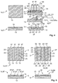
- Fig. 1 shows the inventive contact element 1 in a top view 3 and a cut side view 5 in a first embodiment 7 and a second embodiment 9 of the contact element 1.
- the cut side view 5 corresponds to the first embodiment 7 and the second embodiment 9, both cutting along a line 11 indicated in the both top views 3.
- Fig. 1 shows the substrate 13, the masking layer 15 and the electrically conductive layer 17. In the top views 3, only the masking layer 15 and the electrically conductive layer 17 are visible.
- the first embodiment 7 of the contact element 1 comprises stripe-shaped portions of the electrically conductive layer 19 which constitute the electrically conductive layer 17.
- the second embodiment 9 of the contact element 1 comprises rectangular portions of the electrically conductive layer 19 arranged in a matrix 21 of six times four of such portions 19.
- the twenty-four portions of the electrically conductive layer 19 constitute the electrically conductive layer 17 of the second embodiment 9. For reasons of visibility, not all of the portions 19 of the second embodiment 9 are provided with reference numerals.
- the stripe-shaped portions of the electrically conductive layer 19 separate the masking layer 15 of the first embodiment 7 into stripe-shaped portions of the masking layer 23, whereas the second embodiment 9 of the contact element 1 comprises one unitary masking layer 15, which is, however, interrupted by the rectangular portions of the electrically conductive layer 19.
- the masking layer 15 as well as the electrically conductive layer 17 is directly deposited on the substrate 13 and both layers 15, 17 form alternating regions 25.
- the alternating regions 25 generate a contact pattern 27 which may be symmetric as shown in Fig. 1 , but which may also be asymmetric, i.e. consisting of an arbitrary number of portions of the electrically conductive layer 19 and an arbitrary number of portions of the masking layer 23 in an arbitrary shape of the portions 19, 23.
- the contact elements 1 shown in Fig. 1 may be part of an electric assembly 29, which is indicated in the cut side view 5 of Figure 1 .
- the contact elements 1 shown in Fig. 1 further define a contact side 31.
- the masking layer 15 and the electrically connected layer 17 are deposited on the substrate 13 and form a contact surface 32.
- Fig. 2 shows a third embodiment 10 of the contact element 1 in a cut side view 5.
- the third embodiment 10 additionally comprises an intermediate layer 33 which may be embodied as a nickel or nickel alloy layer 35.
- the contact pattern 27 of the third embodiment 10 may correspond to the contact pattern 27 of the first embodiment 7 or the second embodiment 9 shown in Fig. 1 .
- the intermediate layer 33 is located between the substrate 13 and the masking layer 15 and between the substrate 13 and the electrically conductive layer 17, i.e. the contact surface 32 of the third embodiment 10 is similar or identical to the contact surface 32 of the first 7 and the second embodiment 9 shown in Fig. 1 .
- the portions of the electrically conductive layer 19 correspond to unmasked regions 37.
- the intermediate layer 33 has a first layer thickness 39 which is similar to a second layer thickness 41 of the masking layer 15 and the electrically conductive layer 17. Each of the first 39 and second layer thickness 41 is smaller than the substrate thickness 43 which is indicated by the interruption of the substrate 13.
- the masking layer 15 may contain a polymer 45, wherein the polymer 45 may furthermore comprise a lubricating filler medium 47 and/or an electrically conductive filler medium 48.
- the substrate 13 is preferentially made of copper 49 or a copper alloy 51.
- Preferred materials for the electrically conductive layer 17 are for instance noble metals 59 or tin 61 which is indicated in Fig. 2 for one portion of the electrically conductive layer 19.
- the material of the intermediate layer 33 preferentially contains nickel 55 or a nickel alloy 57, which is indicated in Fig. 2 .
- Application of nickel 55 or nickel alloy 57 as material of the intermediate layer 33 increases the effective hardness 63 of the electrically conductive layer 17, which is indicated in Fig. 2 for one portion of the electrically conductive layer 19.
- Fig. 3 shows three techniques for masking a substrate 13 with a masking layer 15.
- Two techniquee are pressure-based, as for instance spraying 65, wherein the liquid masking material 67 is sprayed through a nozzle 69 onto a pristine substrate 13.
- Spraying 65 has the advantage that only the contact side 31 may be provided with the masking layer 15 (not shown in Fig. 3 ).
- Fig. 3 furthermore shows the technique of printing 66, wherein the liquid masking material 67 is provided via a flexible tube to a multitude of nozzles 69 which may be embodied as printing nozzles 70 allowing for providing the liquid masking material 67 in a structured manner with a resolution of the structures depending on the size of the printing nozzle 70.
- a printing assembly 103 allows for movement of the printing nozzle 70 along an x-direction and a y-direction indicated by arrows in Fig. 3 .
- the printing assembly 103 is shown after the generation of three portions of the masking layer 23. It is to be noted that the printing assembly 103 shown in Fig. 3 is solely depicted schematically and translation means 105 for allowing movement of the printing nozzle 70 along the x-direction and along the y-direction may be embodied in a different way.
- a second possible technique for masking the substrate 13 is dipping 71, wherein the pristine substrate 13 is moved (indicated by an arrow of movement 73) into the liquid masking material 67 which is provided in a container for liquids 75.
- Spraying 65 may be preferred if the second layer thickness 41 (not shown in Fig. 3 ) is to be precisely controlled.
- the liquid masking material 67 may, in the application steps of dipping 71 or spraying 65, already contain the lubricating filler medium 47 and/or the electrically conductive filler medium 48 and/or a photosensitive filler medium 77 which filler media are dissolved in the polymer 45 of the liquid masking material 67.
- Fig. 4 shows three possible techniques for removing parts of the masking layer 15.
- the lefthand side of Fig. 4 shows the top view 3 and the cut side view 5 of a pretreated contact element 1 a as obtained after a processing step as shown in Fig. 3 .
- the pretreated contact element 1 a comprises the substrate 13 and the masking layer 15.
- a first possible technique for removing parts of the masking layer 15 is by photochemical treatment 79, which is partially shown in the upper right panel of Fig. 4 .
- the pretreated contract element 1a is illuminated on the contact side 31 by light 81 of a wavelength region, which alters the properties of the photosensitive filler medium 77 incorporated in the masking layer 15.
- the light 81 is homogeneously illuminating a mask carrier 83 which comprises opaque regions 85 and transparent regions 87.
- the transparent regions 87 may be embodied as through-holes in the simplest embodiment of the mask carrier 83.
- the opaque regions 85 of the mask carrier 83 generate non-illuminated portions 89 located below the opaque regions 85 and illuminated portions 91 which are located below the transparent regions 87. Both portions 89, 91 are located on the contact side 31.
- the middle right panel of Fig. 4 shows the second possible technique for removing parts of the masking layer 15.
- a laser 109 emits the light 81, i.e. in this case laser light 111 onto a scanning mirror device 113 which allows moving the laser light 111 in a scanning manner over the pre-treated contact element 1 a.
- the laser 109 is preferentially embodied as a pulsed laser 109a.
- the pulsed laser 109a has generated one unmasked region 37 and is shown in a state in which a portion of the masking layer 15 is partially ablated and forms a partially ablated portion 115, wherein in this partially ablated portion 115 the masking layer 15 is partially removed on the contact side, whereas a residual fraction 117 of the masking layer still covers the substrate 13.
- the laser light 111 shown in Fig. 4 is schematically depicted and may have a much smaller beam diameter (not shown), which allows for fine structures with a high resolution generated in the masking layer 15. As mentioned in the beginning, the resolution may be even further increased if an electron beam (not shown) is applied instead of a laser 109.
- the lower right panel of Fig. 4 shows a third possible technique for removing parts of the masking layer 15.
- the pretreated contract element 1a is mechanically contacted by a displacement member 95.
- the displacement member 95 is displacing the material of the masking layer 15 and generates unmasked regions 37 which are areas where the masking layer 15 is missing and the substrate 13 is exposed after the displacement member 95 is removed from the pretreated contact element 1 a.
- Fig. 4 shows a hybrid variant of the displacement treatment 93, in which the displacement member 95 is transparent and allows for transmitting the light 81.
- Fig. 4 only a limited area of the displacement member 95 is illuminated by the light 81, whereas the light 81 is transmitted through the transparent displacement member 95 and reaches the portions of the masking layer 23 as well as the unmasked regions 37.
- Such a hybrid variant of the displacement treatment 93 may be beneficial if the material of the masking layer 15 has a low viscosity in order to allow for displacement of the masking layer 15 by the displacement member 95.
- the illumination of the remaining portions of the masking layer 23 may initiate a hardening of the material of the masking layer 15. Such a hardening may be performed simultaneously with the displacement of the masking layer 15 by the displacement member 95.
- Fig. 5 shows a structured contact element 1b in a pre-deposition state 97 and the structured contact element 1b in a final state 99.
- the pre-deposition state 97 and the final state 99 are each shown in a top view 3 and a cut side view 5.
- the pre-deposition state 97 the illuminated portions 91 of the masking layer 15 have been removed.
- the pre-deposition state 97 shown in Fig. 5 may also be obtained by the displacement treatment 93 shown in Fig. 4 , i.e. by mechanically displacing the material of the masking layer 15 for forming the unmasked regions 37.
- the unmasked regions 37 of Fig. 5 are stripe -shaped and expose the substrate 13, which is shown in the top view 3 of the structured contact element 1 b in the pre-deposition state 97.
- a contact material 53 is deposited in between the portions of the masking layer 23, respectively on, the unmasked regions 37, whereas the contact material 53 is not deposited on the portions of the masking layer 23.
- the alternating regions 25 of the different portions 19, 23 form the even and uninterrupted contact surface 32.
Landscapes
- Engineering & Computer Science (AREA)
- Manufacturing & Machinery (AREA)
- Manufacturing Of Electrical Connectors (AREA)
- Contacts (AREA)
Abstract
Description
- The invention relates to a contact element for an electric assembly and a method for production thereof. The invention further relates to a method for producing contact elements for an electric assembly.
- In general, contact elements for electric plug connectors yield high plug-in forces resulting in wear of the contact element if relative movements between the contact element and a counter contact element occur. Especially in miniaturized plug connectors and in plug connectors comprising a multitude of contact elements, e.g. contact pins, the necessary plug-in forces for obtaining a final plug state of the plug connector are beyond customer specifications.
- To overcome this problem, solutions of the art apply additional lubrication or mechanical means, for instance levers for obtaining the final plug state with plug-in forces within customer specifications.
- Additional mechanical means render the plug connector more complicated and expensive, whereas lubricating means need to meet the demands with respect to shelf life and temperature stability.
- Especially for miniaturized plug connectors applied in the automotive sector, contact surfaces are subject to limited wear resistance and limiting plug-in forces. The contacting portions, or contact surfaces of plug connectors of the art are in general embodied as stationary contact surfaces and not in a sliding manner. Application of a multitude of contact elements, for instance contact pins, increases the necessary plug-in force according to the number of contact elements.
- Additionally, plug connectors with contact elements of the art generally apply noble metals, for instance, gold, silver or palladium or exemplarily the metal tin to the entire contact surface. Those metal coatings increase the resistivity of the contact element against corrosion without remarkably reducing the electric conductivity of the contact element. Those noble metals, however, are precious and increase the cost of said plug connectors.
- One object of the present invention is therefore to reduce the amount of noble metals used in the contact element. Furthermore, one object of the present invention is to provide a lubricant with the contact element, the lubricant having a high shell life, i.e. high storage ability, providing protection against corrosion and is chemically longtime stable.
- The inventive contact element solves the above problems by comprising a substrate, at least one electrically conductive layer and at least one masking layer, wherein a contact side of the contact element is at least partly covered by the at least one masking layer and the at least one electrically conductive layer, and wherein the at least one masking layer and the at least one electrically conductive layer form a contact surface, the contact surface comprising alternating regions of the at least one masking layer and the at least one electrically conductive layer.
- It is also conceivable that the contact element comprises two or more contact surfaces, each comprising at least one masking layer and at least one electrically conductive layer.
- The contact side may be at least partly covered by the at least one masking layer and the at least one electrically conductive layer directly or indirectly.
- The alternating regions of the at least one masking layer and the at least one electrically conductive layer have to be understood as a local arrangement of portions of the at least one electrically conductive layer and the at least one masking layer on the contact surface.
- As a non-limiting example, the contact element may comprise a certain number of electrically conductive portions, embodied for instance as a stripe, rectangle, or another geometrical form which electrically conductive portions may be surrounded by the masking layer. However, it is also possible, that masking portions forming the masking layer may be surrounded by electrically conductive portions forming the electrically conductive layer.
- A layer is to be understood as a thin two-dimensional structure of deposited material, whereas the expression thin relates to a thickness much smaller than the thickness of the substrate. In general, layer thicknesses of contact elements are in the order of approximately 1 µm up to 100 µm.
- The inventive method mentioned above solves the problems by comprising the steps of masking a substrate with a masking layer, forming at least one unmasked region by partially removing the masking layer, and depositing a conductive layer in at least part of the at least one unmasked region.
- Masking the substrate with the masking layer may be performed by emerging the substrate into a bath of the masking material or by spraying the masking material onto the substrate. Those two possibilities of masking the substrate are solely to be understood as non-limiting exemplary masking steps.
- The masking layer may be homogenously deposited on the substrate by the two exemplary techniques mentioned above or may be applied directly via printing techniques. Possible printing techniques for application of the masking layer to the substrate are for instance ink jet printing, jet printing or gravure printing. The above mentioned printing techniques may also be applied to print a homogenous masking layer on the substrate. Printing techniques as mentioned above allow for direct, time-saving and cost-reducing application of the masking layer with a resolution only limited by the printing technique and the printer device used.
- Forming the at least one unmasked region by partially removing the masking layer may, as a non-limiting example, be performed by direct laser ablation. Another ablation technique for forming the at least one unmasked region is electron beam ablation. Both ablation techniques are based on an ultra fast heating of material, which heating generates a plasma and an abrupt evaporation of the heated material. In the case of laser ablation, the material is heated by laser radiation, whereas in the case of electron beam ablation the energy for the generation of the plasma is provided by an electron beam.
- Electron beam ablation yields a higher obtainable resolution at the expense of a more complicated system.
- The following description will focus on laser ablation only but may be adapted to electron beam ablation as well.
- Laser ablation in general utilizes short or ultra short laser pulses with pulse durations in the ns-range or fs-range, as for instance emitted by solid state lasers based on rare earth doped laser active materials or titanium sapphire, respectively by excimer lasers.
- In the following, different embodiment of the present invention will be presented and the described, wherein each embodiment is advantageous on its own and technical features of the different embodiments may be combined or omitted as long as the technical effect of the omitted technical feature is not relevant to the invention.
- In a first embodiment of the inventive contact element, the at least one electrically conductive layer is located in unmasked regions of the contact surface.
- Unmasked areas of the contact surface are regions where the masking layer is missing.
- The at least one masking layer and the at least one electrically conductive layer may be located adjacent to each other on the contact surface.
- In other words, the at least one masking layer may be located seamlessly next to the at least one electrically conductive layer. The substrate is thus entirely covered and protected by the at least one masking layer and the at least one electrically conductive layer.
- According to the number of portions of the masking layer and portions of the electrically conductive layer, as well as according to the shape of the portions, one portion (masking or electrically conductive) may be located adjacent to a different number of other portions (electrically conductive or masking).
- The portions of the masking layer and the portions of the electrically conductive layer represent the alternating regions mentioned in the beginning.
- In a second embodiment of the inventive contact element, the masking layer comprises a lubricating filler medium. The lubricating filler medium may be contained in a polymer.
- The polymer may furthermore comprise, e.g. consist of a lubricating filler medium.
- The masking layer may thus act as a lubricating depot providing lubrication to the electrically conductive layer located adjacent to the masking layer.
- The lubricating filler medium may comprise a wet or a dry lubricant, e.g. grease or graphite. The lubricating filler medium may comprise lubricating particles immersed in the material of the masking layer.
- As the at least one masking layer and the at least one electrically conductive layer form the contact surface, the lubricating filler medium is located adjacent to at least one portion of the electrically conductive layer, preferentially embedded in between a multitude of electrically conductive portions. Thus, the contact surface mechanically abuts a counter contact surface during a plug- in operation by means of the electrically conductive layer.
- The masking layer may be in mechanical contact with the counter contact surface, but the contact force is exerted through the electrically conductive portions of the contact surface, respectively. Consequently, the material of the masking layer comprising the lubricating filler medium is not displaced by the counter contact surface, but is still in mechanical contact with it.
- The polymer that can be used for the masking layer may be designed for different applications, for instance for different temperature ranges in which the contact element may be applied as well as ambient conditions like humidity, electromagnetic radiation or atmosphere. The polymer may be any commercially available polymer (e.g. PMMA, PE, PVC, PET, PC, PET, PU or similar), suitable for receiving the lubricating filler medium.
- In another embodiment of the present contact element, the contact element may be embodied as a sliding contact. In such a sliding contact, the contacting portions or the contact points do move around a corresponding rest position.
- Also for plug-in connectors not specifically designed as sliding contact, those properties may have the advantage of an increased stability against vibrations during which the contacting portion or contact point is moved out of its rest position.
- In a third embodiment of the inventive contact element, a masking layer comprises an electrically conductive filler medium.
- Such an electrically conductive filler medium may comprise particles or nanoparticles, for instance, carbon derivates like graphite or nanotubes, or simply metal particles.
- The masking layer of this embodiment therefore fulfills two functionalities, i.e. lubricating the contact surface for reducing the plug-in forces and providing an additional electrical connection between the contact surface of the contact element and the counter contact surface of the counter contact element.
- In another embodiment of the inventive contact element, the substrate is made of one of copper or a copper alloy.
- Copper or a copper alloy are generally used for electrical contacting means as they yield low ohmic resistance, a high electric conductivity and may be easily manufactured. However, copper shows the tendency of oxidation in ambient air and is, due to its hardness, not suitable for repeated plug-in operations. Inter alia for this reason, the copper or copper alloy is at least partly covered by the at least one masking layer and the at least one electrically conductive layer.
- In another embodiment of the inventive contact element, the electrically conductive layer comprises a contact material different from the material of the substrate. That is to say a contact material is deposited onto portions of the substrate which are unmasked, i.e. not covered by the masking layer.
- A copper alloy of different composition than the substrate may also be used as material for the electrically conductive layer.
- The electrically conductive layer may contain a noble metal, for instance, gold, silver or palladium or a less toxic heavy metal such as tin. The material of the electrically conductive layer therefore protects the unmasked areas of the substrate against environmental conditions.
- The material applied in the electrically conductive layer may furthermore contain an alloy of the above mentioned metals.
- In another embodiment of the inventive contact element, an intermediate layer is arranged between the substrate and at least one of the at least one masking layer and the at least one electrically conductive layer.
- The intermediate layer may entirely cover the portions of the substrate which form the contact surface. The intermediate layer may preferentially be located between the substrate and the masking layer, and between the substrate and the electrically conductive layer. The intermediate layer may support the electrically conductive layer and may contain an electrically conductive material, preferentially a metal with a similar electric conductivity as the substrate and/or the electrically conductive layer.
- In another embodiment of the inventive contact element, the intermediate layer has a thickness between approximately 1 µm and approximately 3 µm. Such a thickness of the intermediate layer may be applied to increase the effective hardness of the electrically conductive layer.
- The intermediate layer embodied in the above given thickness does not influence the flexibility and elasticity of the substrate but still protects the substrate against environmental influences.
- The hardness of the intermediate layer may be higher than the hardness of the substrate, therefore increasing the resistivity of the contact element against wear, for instance, abrasion due to repeated plug operation.
- In another embodiment of the inventive contact element the intermediate layer contains one of nickel or a nickel alloy. Nickel or nickel alloy provide the above-mentioned advantages of protecting the substrate against environmental influences, increasing the effective hardness of the electrically conductive layer deposited on the side of the intermediate layer opposite to the substrate.
- Such a nickel or nickel alloy, generally the intermediate layer, further transfers plug-in forces exerted from the electrically conductive layer to the intermediate layer and to the substrate. The latter may deflect or resiliently deform entirely, even if the exerted plug-in force is applied selectively or punctually.
- The intermediate layer thus distributes the plug-in force to the substrate over an area larger than the area of the portions of the electrically conductive layer.
- A first embodiment of the inventive method further comprises the step of providing an intermediate layer between the substrate and at least one of the masking layer and the electrically conductive layer.
- Preferentially, the intermediate layer contains one of a nickel layer or a nickel alloy layer, which layer is embodied with a thickness on the order of 1 µm up to several micrometers.
- The intermediate layer may be deposited on the substrate by means of galvanic deposition, chemical or physical vapor deposition, ion beam deposition, sputtering or similar techniques.
- A second embodiment of the inventive method further comprises the step of providing at least the masking layer with at least one of an electrically conductive filler medium and a lubricating filler medium.
- An electrically conductive filler medium has the advantage that an electrical connection between the contact element and an according counter contact element may be established even if the electrically conductive layer of the contact element does not abut the counter contact element. Furthermore, the electrically conductive filler medium increases the possible current that is transmittable via the contact surface.
- The lubricating filler medium in the masking layer transforms the latter into a lubricating depot which may continuously guarantee lubrication of the electrically conductive layer. Furthermore, as the electrically conductive layer is deposited in at least part of the unmasked regions of the masking layer, the lubricating filler medium, as part of the masking layer material is not displaced when the electrically conductive layer abuts the counter contact element.
- The electrically conductive filler medium and/or the lubricating filler medium may be provided in the masking layer material prior to masking of the substrate with the masking layer. That is to say, the corresponding filler media are incorporated into the masking layer material before applying the latter to the substrate or to the intermediate layer.
- It is also conceivable that the electrically conductive filler medium and/or the lubricating filler medium may be incorporated into the masking layer after masking the substrate with the masking layer. Incorporation of said filler media may be performed by assimilation, implantation, absorption or adsorption.
- The filler media may be homogeneously provided in the masking layer material or solely in a top portion of the masking layer, wherein the top portion is to be understood as the part of the masking layer farthest away from the substrate.
- A third embodiment of the inventive method further comprises the step of providing the masking layer with a photosensitive filler medium.
- The photosensitive filler medium may especially contain or consists of a photoresist or a hardening polymer.
- A photosensitive filler medium is to be understood as a material which changes its physical and/or mechanical and/or chemical properties upon illumination with light of a certain wavelength range. As a possible, non-limiting example, a photosensitive filler medium may increase its resistivity against a chemical, i.e. decreasing its solubility in this chemical. An illuminated area of such a photosensitive filler medium will consequently not be solved in the chemical and will remain on the substrate or the intermediate layer.
- In another embodiment of the inventive method, the step of partially removing the masking layer comprises displacing parts of the masking layer by a displacement member.
- The displacement member may be embodied as an embossing die, which may displace the masking layer material such that it exposes the substrate or intermediate layer at at least one processing portion, which processing portion may be further machined or treated.
- The displacement member may be transparent for light of the wavelength range which influences the photosensitive filler medium. Such a transparent displacement member allows illumination of the masking layer through the transparent displacement member and may for instance result in a hardening of the masking layer material.
- Another embodiment of the inventive method further comprises the step of illuminating the masking layer and photochemically developing one of illuminated portions or non-illuminated portions of the masking layer for forming the at least on unmasked region.
- Preferentially the masking layer may be illuminated with light of a wavelength range affecting the photosensitive medium.
- As described above, illuminating the masking layer with light of a wavelength range affecting the photosensitive medium may alter the chemical properties of the illuminated part of the masking layer such that the resistivity against a developing chemical is altered.
- In case of a positive photoresist, the resistivity is decreased upon illumination and in case of a negative photoresist, it is increased.
- It is noted that a masking pattern may be generated via interference of the illuminating light, which is emitted from a laser in this case, or may be generated by a mask carrier blocking portions of the incident light and forming a light pattern on the masking layer.
- Depending on whether the photosensitive filler medium is a positive or negative photoresist, either the illuminated portions of the masking layer or the non-illuminated portions of the masking layer are affected by the developing chemical. The developing chemical may preferentially be a liquid chemical, which may be provided in a bath through which bath the contact element may be moved.
- Preferentially, conventional photoresists may be used, which are affected by ultraviolet and/or violet electromagnetic radiation.
- Another possibility of removing parts of the masking layer is direct ablation of the masking layer in the corresponding processing portions, i.e. the portions where the masking layer is to be removed for exposing the substrate or the intermediate layer. On those processing portions, the electrically conductive layer is to be deposited.
- In the following, the inventive contact element and method is described with reference to the accompanied figures. The figures show embodiments of the contact element and the inventive method for producing the same which are advantageous on their own. Technical features of the individual embodiments may be combined arbitrarily and may be omitted if the technical effect of the corresponding omitted technical feature is not relevant. Same technical features or features with the same technical effect are denoted with the same reference numeral.
- In the figures:
- Fig. 1
- shows two embodiments of the inventive contact elements in a top view and in a cut side view;
- Fig. 2
- illustrates a cut side view of a third embodiment of the inventive contact element;
- Fig. 3
- shows two possible techniques of masking a substrate with a masking layer;
- Fig. 4
- shows two possible techniques of removing parts of the masking layer; and
- Fig. 5
- shows deposition of a conductive layer to the contact element obtained in
Fig. 4 . -
Fig. 1 shows the inventive contact element 1 in atop view 3 and acut side view 5 in a first embodiment 7 and a second embodiment 9 of the contact element 1. - The
cut side view 5 corresponds to the first embodiment 7 and the second embodiment 9, both cutting along aline 11 indicated in the bothtop views 3. - In the
cut side view 5,Fig. 1 shows thesubstrate 13, themasking layer 15 and the electricallyconductive layer 17. In thetop views 3, only themasking layer 15 and the electricallyconductive layer 17 are visible. - The first embodiment 7 of the contact element 1 comprises stripe-shaped portions of the electrically
conductive layer 19 which constitute the electricallyconductive layer 17. - The second embodiment 9 of the contact element 1 comprises rectangular portions of the electrically
conductive layer 19 arranged in a matrix 21 of six times four ofsuch portions 19. The twenty-four portions of the electricallyconductive layer 19 constitute the electricallyconductive layer 17 of the second embodiment 9. For reasons of visibility, not all of theportions 19 of the second embodiment 9 are provided with reference numerals. - The stripe-shaped portions of the electrically
conductive layer 19 separate themasking layer 15 of the first embodiment 7 into stripe-shaped portions of themasking layer 23, whereas the second embodiment 9 of the contact element 1 comprises oneunitary masking layer 15, which is, however, interrupted by the rectangular portions of the electricallyconductive layer 19. - In the
cut side view 5 of the inventive contact element, which is obtained by cutting either of the first 7 or second embodiment 9 along theline 11, one can see that themasking layer 15 as well as the electricallyconductive layer 17 is directly deposited on thesubstrate 13 and bothlayers form alternating regions 25. - The alternating
regions 25 generate acontact pattern 27 which may be symmetric as shown inFig. 1 , but which may also be asymmetric, i.e. consisting of an arbitrary number of portions of the electricallyconductive layer 19 and an arbitrary number of portions of themasking layer 23 in an arbitrary shape of theportions - The contact elements 1 shown in
Fig. 1 may be part of anelectric assembly 29, which is indicated in thecut side view 5 ofFigure 1 . - The contact elements 1 shown in
Fig. 1 further define acontact side 31. On thecontact side 31, themasking layer 15 and the electrically connectedlayer 17 are deposited on thesubstrate 13 and form acontact surface 32. -
Fig. 2 shows a third embodiment 10 of the contact element 1 in acut side view 5. The third embodiment 10 additionally comprises an intermediate layer 33 which may be embodied as a nickel or nickel alloy layer 35. - The
contact pattern 27 of the third embodiment 10 may correspond to thecontact pattern 27 of the first embodiment 7 or the second embodiment 9 shown inFig. 1 . - The intermediate layer 33 is located between the
substrate 13 and themasking layer 15 and between thesubstrate 13 and the electricallyconductive layer 17, i.e. thecontact surface 32 of the third embodiment 10 is similar or identical to thecontact surface 32 of the first 7 and the second embodiment 9 shown inFig. 1 . - In
Fig. 1 and Fig. 2 , the portions of the electricallyconductive layer 19 correspond to unmaskedregions 37. - The intermediate layer 33 has a
first layer thickness 39 which is similar to asecond layer thickness 41 of themasking layer 15 and the electricallyconductive layer 17. Each of the first 39 andsecond layer thickness 41 is smaller than thesubstrate thickness 43 which is indicated by the interruption of thesubstrate 13. - The
masking layer 15 may contain a polymer 45, wherein the polymer 45 may furthermore comprise a lubricating filler medium 47 and/or an electrically conductive filler medium 48. - The
substrate 13 is preferentially made of copper 49 or a copper alloy 51. The portions of the electricallyconductive layer 19, i.e. the electricallyconductive layer 17 itself, contains acontact material 53 which is different than thecontact material 53 of thesubstrate 13. Preferred materials for the electricallyconductive layer 17 are for instance noble metals 59 or tin 61 which is indicated inFig. 2 for one portion of the electricallyconductive layer 19. - The material of the intermediate layer 33 preferentially contains nickel 55 or a nickel alloy 57, which is indicated in
Fig. 2 . Application of nickel 55 or nickel alloy 57 as material of the intermediate layer 33 increases theeffective hardness 63 of the electricallyconductive layer 17, which is indicated inFig. 2 for one portion of the electricallyconductive layer 19. -
Fig. 3 shows three techniques for masking asubstrate 13 with amasking layer 15. Two techniquee are pressure-based, as for instance spraying 65, wherein theliquid masking material 67 is sprayed through anozzle 69 onto apristine substrate 13. Spraying 65 has the advantage that only thecontact side 31 may be provided with the masking layer 15 (not shown inFig. 3 ). -
Fig. 3 furthermore shows the technique of printing 66, wherein theliquid masking material 67 is provided via a flexible tube to a multitude ofnozzles 69 which may be embodied as printing nozzles 70 allowing for providing theliquid masking material 67 in a structured manner with a resolution of the structures depending on the size of the printing nozzle 70. Aprinting assembly 103 allows for movement of the printing nozzle 70 along an x-direction and a y-direction indicated by arrows inFig. 3 . InFig. 3 , theprinting assembly 103 is shown after the generation of three portions of themasking layer 23. It is to be noted that theprinting assembly 103 shown inFig. 3 is solely depicted schematically and translation means 105 for allowing movement of the printing nozzle 70 along the x-direction and along the y-direction may be embodied in a different way. - A second possible technique for masking the
substrate 13 is dipping 71, wherein thepristine substrate 13 is moved (indicated by an arrow of movement 73) into theliquid masking material 67 which is provided in a container forliquids 75. - The technique of dipping 71 masks the
entire substrate 13 moved into theliquid masking material 67. Spraying 65 on the other hand may be preferred if the second layer thickness 41 (not shown inFig. 3 ) is to be precisely controlled. - The
liquid masking material 67 may, in the application steps of dipping 71 or spraying 65, already contain the lubricating filler medium 47 and/or the electrically conductive filler medium 48 and/or aphotosensitive filler medium 77 which filler media are dissolved in the polymer 45 of theliquid masking material 67. -
Fig. 4 shows three possible techniques for removing parts of themasking layer 15. The lefthand side ofFig. 4 shows thetop view 3 and thecut side view 5 of apretreated contact element 1 a as obtained after a processing step as shown inFig. 3 . - The
pretreated contact element 1 a comprises thesubstrate 13 and themasking layer 15. - A first possible technique for removing parts of the
masking layer 15 is byphotochemical treatment 79, which is partially shown in the upper right panel ofFig. 4 . - In the
photochemical treatment 79 the pretreatedcontract element 1a is illuminated on thecontact side 31 bylight 81 of a wavelength region, which alters the properties of thephotosensitive filler medium 77 incorporated in themasking layer 15. The light 81 is homogeneously illuminating amask carrier 83 which comprisesopaque regions 85 andtransparent regions 87. Thetransparent regions 87 may be embodied as through-holes in the simplest embodiment of themask carrier 83. - The
opaque regions 85 of themask carrier 83 generatenon-illuminated portions 89 located below theopaque regions 85 and illuminatedportions 91 which are located below thetransparent regions 87. Bothportions contact side 31. - Depending on the type of the photosensitive filler medium 77 (positive or negative) either the
illuminated portions 91 or thenon-illuminated portions 89 will be removed in a developing step, which is, however, not shown inFig. 4 . - The middle right panel of
Fig. 4 shows the second possible technique for removing parts of themasking layer 15. In the treatment applyinglaser ablation 107, a laser 109 emits the light 81, i.e. in this case laser light 111 onto ascanning mirror device 113 which allows moving the laser light 111 in a scanning manner over thepre-treated contact element 1 a. - The laser 109 is preferentially embodied as a pulsed laser 109a.
- In the middle right panel of
Fig. 4 , the pulsed laser 109a has generated oneunmasked region 37 and is shown in a state in which a portion of themasking layer 15 is partially ablated and forms a partially ablatedportion 115, wherein in this partially ablatedportion 115 themasking layer 15 is partially removed on the contact side, whereas aresidual fraction 117 of the masking layer still covers thesubstrate 13. - The laser light 111 shown in
Fig. 4 , is schematically depicted and may have a much smaller beam diameter (not shown), which allows for fine structures with a high resolution generated in themasking layer 15. As mentioned in the beginning, the resolution may be even further increased if an electron beam (not shown) is applied instead of a laser 109. - The lower right panel of
Fig. 4 shows a third possible technique for removing parts of themasking layer 15. In the displacement treatment 93 the pretreatedcontract element 1a is mechanically contacted by adisplacement member 95. - The
displacement member 95 is displacing the material of themasking layer 15 and generates unmaskedregions 37 which are areas where themasking layer 15 is missing and thesubstrate 13 is exposed after thedisplacement member 95 is removed from the pretreatedcontact element 1 a. -
Fig. 4 shows a hybrid variant of the displacement treatment 93, in which thedisplacement member 95 is transparent and allows for transmitting the light 81. - In
Fig. 4 only a limited area of thedisplacement member 95 is illuminated by the light 81, whereas the light 81 is transmitted through thetransparent displacement member 95 and reaches the portions of themasking layer 23 as well as the unmaskedregions 37. - Such a hybrid variant of the displacement treatment 93 may be beneficial if the material of the
masking layer 15 has a low viscosity in order to allow for displacement of themasking layer 15 by thedisplacement member 95. The illumination of the remaining portions of themasking layer 23 may initiate a hardening of the material of themasking layer 15. Such a hardening may be performed simultaneously with the displacement of themasking layer 15 by thedisplacement member 95. -
Fig. 5 shows astructured contact element 1b in apre-deposition state 97 and thestructured contact element 1b in afinal state 99. Thepre-deposition state 97 and thefinal state 99 are each shown in atop view 3 and acut side view 5. - In the
pre-deposition state 97 the illuminatedportions 91 of themasking layer 15 have been removed. Thepre-deposition state 97 shown inFig. 5 may also be obtained by the displacement treatment 93 shown inFig. 4 , i.e. by mechanically displacing the material of themasking layer 15 for forming the unmaskedregions 37. - The unmasked
regions 37 ofFig. 5 are stripe -shaped and expose thesubstrate 13, which is shown in thetop view 3 of thestructured contact element 1 b in thepre-deposition state 97. - In the next fabrication step (which is not shown in
Fig. 5 ) acontact material 53 is deposited in between the portions of themasking layer 23, respectively on, the unmaskedregions 37, whereas thecontact material 53 is not deposited on the portions of themasking layer 23. - After the deposition step, the
masking layer 15 and the electricallyconductive layer 17, which are composed of the correspondingportions regions 25 and thecontact pattern 27 of the corresponding contact element 1. - As can be seen in
Fig. 5 , the alternatingregions 25 of thedifferent portions uninterrupted contact surface 32. -
- 1
- contact element
- 1a
- pretreated contact element
- 1b
- structured contact element
- 3
- top view
- 5
- cut side view
- 7
- first embodiment
- 9
- second embodiment
- 10
- third embodiment
- 11
- line
- 13
- substrate
- 15
- masking layer
- 17
- electrically conductive layer
- 19
- portions of the electrically conductive layer
- 21
- matrix
- 23
- portions of the masking layer
- 25
- alternating region
- 27
- contact pattern
- 29
- electric assembly
- 31
- contact side
- 32
- contact surface
- 33
- intermediate layer
- 35
- nickel or nickel alloy layer
- 37
- unmasked region
- 39
- first layer thickness
- 41
- second layer thickness
- 43
- substrate thickness
- 45
- polymer
- 47
- lubricating filler medium
- 48
- electrically conductive filler medium
- 49
- copper
- 51
- copper alloy
- 53
- contact material
- 55
- nickel
- 57
- nickel alloy
- 59
- noble metal
- 61
- tin
- 63
- effective hardness
- 65
- spraying
- 66
- printing
- 67
- liquid masking material
- 69
- nozzle
- 70
- printing nozzle
- 71
- dipping
- 73
- arrow of movement
- 75
- container for liquids
- 77
- photosensitive filler medium
- 79
- photochemical treatment
- 81
- light
- 83
- mask carrier
- 85
- opaque region
- 87
- transparent region
- 89
- non-illuminated portion
- 91
- illuminated portion
- 93
- displacement treatment
- 95
- displacement member
- 97
- pre-deposition state
- 99
- final state
- 101
- flexible tube
- 103
- printing assembly
- 105
- translation means
- 107
- laser ablation
- 109
- laser
- 109a
- pulsed laser
- 111
- laser light
- 113
- scanning mirror device
- 115
- partially ablated portion
- 117
- residual fraction
- x
- x-direction
- y
- y-direction
Claims (15)
- Contact element (1) for an electric assembly (29), the contact element (1) comprising a substrate (13), at least one electrically conductive layer (17) and at least one masking layer (15), wherein a contact side (31) of the contact element (1) is at least partly covered by the at least one masking layer (15) and the at least one electrically conductive layer (17), and wherein the at least one masking layer (15) and the at least one electrically conductive layer (17) form a contact surface (32), the contact surface (32) comprising alternating regions (25) of the at least one masking layer (15) and the at least one electrically conductive layer (17).
- Contact element (1) according to claim 1, wherein the at least one electrically conductive layer (17) is located in unmasked regions (37) of the contact surface (32).
- Contact element (1) according to claim 1 or 2, wherein the masking layer (15) comprises a lubricating filler medium (47).
- Contact element (1) according to any one of claims 1 to 3, wherein the masking layer (15) comprises an electrically conductive filler medium (48).
- Contact element (1) according to any one of claims 1 to 4, wherein the substrate (13) contains one of copper (49) or a copper alloy (51).
- Contact element (1) according to any one of claims 1 to 5, wherein the electrically conductive layer (17) comprises a contact material (53) different from the material of the substrate (13).
- Contact element (1) according to any one of claims 1 to 6, wherein an intermediate layer (33) is arranged between the substrate (13) and at least one of the at least one masking layer (15) and the at least one electrically conductive layer (17).
- Contact element (1) according to claim 7, wherein the intermediate layer (33) has a thickness (39) between approximately 1 µm and approximately 3 µm.
- Contact element (1) according to claim 7 or 8, wherein the intermediate layer (33) contains one of nickel (55) or a nickel alloy (57).
- Method for producing a contact element (1) for an electric assembly (29), the method comprising the steps of:- masking a substrate (13) with a masking layer (15);- forming at least one unmasked region (37) by partially removing the masking layer (15); and- depositing an electrically conductive layer (17) in at least part of the at least one unmasked region (37).
- Method according to claim 10, further comprising the step of: providing an intermediate layer (33) between the substrate (13) and at least one of the masking layer (15) and the electrically conductive layer (17).
- Method according to claim 10 or 11, further comprising the step of: providing the masking layer (15) with at least one of an electrically conductive filler medium (48) and a lubricating filler medium (47).
- Method according to any one of claims 10 to 12, further comprising the step of: providing the masking layer (15) with a photosensitive filler medium (77).
- Method according to any one of claims 10 to 13, wherein partially removing the masking layer comprises displacing parts of the masking layer (15) by a displacement member.
- Method according to claim 13 or 14, further comprising the step of: illuminating the masking layer (15) and photochemically developing one of illuminated portions (91) or non-illuminated portions (89) of the masking layer (15) and selectively unmasking for forming the at least one unmasked region (37).
Priority Applications (5)
| Application Number | Priority Date | Filing Date | Title |
|---|---|---|---|
| EP16172753.2A EP3252873B1 (en) | 2016-06-02 | 2016-06-02 | Lubricated contact element and method for production thereof |
| CN201780033072.8A CN109196725B (en) | 2016-06-02 | 2017-06-01 | Lubricating contact element and method of making the same |
| JP2019514860A JP6759455B2 (en) | 2016-06-02 | 2017-06-01 | Lubricated contact element and its manufacturing method |
| PCT/EP2017/063389 WO2017207731A1 (en) | 2016-06-02 | 2017-06-01 | Lubricated contact element and method for production thereof |
| US16/203,791 US10958006B2 (en) | 2016-06-02 | 2018-11-29 | Contact element and method for production thereof |
Applications Claiming Priority (1)
| Application Number | Priority Date | Filing Date | Title |
|---|---|---|---|
| EP16172753.2A EP3252873B1 (en) | 2016-06-02 | 2016-06-02 | Lubricated contact element and method for production thereof |
Publications (2)
| Publication Number | Publication Date |
|---|---|
| EP3252873A1 true EP3252873A1 (en) | 2017-12-06 |
| EP3252873B1 EP3252873B1 (en) | 2019-07-24 |
Family
ID=56098130
Family Applications (1)
| Application Number | Title | Priority Date | Filing Date |
|---|---|---|---|
| EP16172753.2A Active EP3252873B1 (en) | 2016-06-02 | 2016-06-02 | Lubricated contact element and method for production thereof |
Country Status (5)
| Country | Link |
|---|---|
| US (1) | US10958006B2 (en) |
| EP (1) | EP3252873B1 (en) |
| JP (1) | JP6759455B2 (en) |
| CN (1) | CN109196725B (en) |
| WO (1) | WO2017207731A1 (en) |
Families Citing this family (3)
| Publication number | Priority date | Publication date | Assignee | Title |
|---|---|---|---|---|
| DE102020134045B3 (en) | 2020-12-17 | 2022-05-12 | Te Connectivity Germany Gmbh | Lubricant applicator and method for applying a solid lubricant and applicator device, arrangement and loading station |
| US12160061B2 (en) * | 2022-02-23 | 2024-12-03 | Te Connectivity Solutions Gmbh | Metal composite for use with separable electrical interfaces |
| DE102024000440B3 (en) | 2024-02-09 | 2025-03-27 | Mercedes-Benz Group AG | Charging socket for a battery-powered vehicle |
Citations (4)
| Publication number | Priority date | Publication date | Assignee | Title |
|---|---|---|---|---|
| JPS5569186A (en) * | 1978-11-17 | 1980-05-24 | Nippon Kokuen Kogyo Kk | Method of making electrode connector for filmmlike liquid crystal display tube |
| JP2004315941A (en) * | 2003-04-18 | 2004-11-11 | Matsushita Electric Works Ltd | Method of producing terminal for soldering |
| US20120119367A1 (en) * | 2010-11-15 | 2012-05-17 | Tessera Research Llc | Conductive pads defined by embedded traces |
| US20150357737A1 (en) * | 2013-01-10 | 2015-12-10 | Autonetworks Technologies, Ltd. | Connector terminal and method for producing connector terminal |
Family Cites Families (22)
| Publication number | Priority date | Publication date | Assignee | Title |
|---|---|---|---|---|
| JPS5569186U (en) * | 1978-11-06 | 1980-05-13 | ||
| US4687274A (en) * | 1984-05-10 | 1987-08-18 | Massachusetts Institute Of Technology | Electrical contacts |
| US5632631A (en) * | 1994-06-07 | 1997-05-27 | Tessera, Inc. | Microelectronic contacts with asperities and methods of making same |
| US6238971B1 (en) * | 1997-02-11 | 2001-05-29 | Micron Technology, Inc. | Capacitor structures, DRAM cell structures, and integrated circuitry, and methods of forming capacitor structures, integrated circuitry and DRAM cell structures |
| US6309975B1 (en) * | 1997-03-14 | 2001-10-30 | Micron Technology, Inc. | Methods of making implanted structures |
| JP3411825B2 (en) * | 1998-06-30 | 2003-06-03 | 株式会社オートネットワーク技術研究所 | Manufacturing method of mating connection terminals |
| JP2000215462A (en) * | 1999-01-25 | 2000-08-04 | Pioneer Electronic Corp | Optical disk and optical disk player |
| US6356002B1 (en) * | 1999-02-08 | 2002-03-12 | Northrop Grumman Corporation | Electrical slip ring having a higher circuit density |
| JP2001216773A (en) | 2000-01-31 | 2001-08-10 | Aiwa Co Ltd | Audio equipment |
| US20020115293A1 (en) * | 2001-01-03 | 2002-08-22 | Bahram Ghodsian | Device to rapidly and accurately sequence long DNA fragments |
| DE10146274A1 (en) * | 2001-09-19 | 2003-04-10 | Bosch Gmbh Robert | Metallic surface of a body, method for producing a structured metallic surface of a body and its use |
| CN1692529B (en) * | 2002-10-10 | 2010-04-28 | 松下电工株式会社 | Method for manufacturing soldered component |
| JP2004265729A (en) * | 2003-02-28 | 2004-09-24 | Jst Mfg Co Ltd | Anisotropic conductive sheet |
| JP2009059479A (en) * | 2007-08-29 | 2009-03-19 | Auto Network Gijutsu Kenkyusho:Kk | Terminal pair |
| US8558960B2 (en) | 2010-09-13 | 2013-10-15 | Semiconductor Energy Laboratory Co., Ltd. | Liquid crystal display device and method for manufacturing the same |
| JP5658582B2 (en) | 2011-01-31 | 2015-01-28 | ルネサスエレクトロニクス株式会社 | Semiconductor device manufacturing method and semiconductor device |
| US9634412B2 (en) * | 2011-07-15 | 2017-04-25 | Tessera, Inc. | Connector structures and methods |
| US20150236439A1 (en) * | 2012-08-31 | 2015-08-20 | Autonetworks Technologies, Ltd. | Plated terminal for connector, and terminal pair |
| JP5692192B2 (en) * | 2012-09-21 | 2015-04-01 | 株式会社オートネットワーク技術研究所 | Method for manufacturing connector terminal and method for manufacturing connector terminal material |
| JP2015059260A (en) * | 2013-09-20 | 2015-03-30 | 株式会社オートネットワーク技術研究所 | Electrical contact material for connector and manufacturing method thereof |
| WO2015163454A1 (en) * | 2014-04-24 | 2015-10-29 | 矢崎総業株式会社 | Contact connection structure |
| JP6651167B2 (en) | 2015-03-23 | 2020-02-19 | スタンレー電気株式会社 | Semiconductor light emitting device and method of manufacturing the same |
-
2016
- 2016-06-02 EP EP16172753.2A patent/EP3252873B1/en active Active
-
2017
- 2017-06-01 CN CN201780033072.8A patent/CN109196725B/en active Active
- 2017-06-01 JP JP2019514860A patent/JP6759455B2/en active Active
- 2017-06-01 WO PCT/EP2017/063389 patent/WO2017207731A1/en not_active Ceased
-
2018
- 2018-11-29 US US16/203,791 patent/US10958006B2/en active Active
Patent Citations (4)
| Publication number | Priority date | Publication date | Assignee | Title |
|---|---|---|---|---|
| JPS5569186A (en) * | 1978-11-17 | 1980-05-24 | Nippon Kokuen Kogyo Kk | Method of making electrode connector for filmmlike liquid crystal display tube |
| JP2004315941A (en) * | 2003-04-18 | 2004-11-11 | Matsushita Electric Works Ltd | Method of producing terminal for soldering |
| US20120119367A1 (en) * | 2010-11-15 | 2012-05-17 | Tessera Research Llc | Conductive pads defined by embedded traces |
| US20150357737A1 (en) * | 2013-01-10 | 2015-12-10 | Autonetworks Technologies, Ltd. | Connector terminal and method for producing connector terminal |
Also Published As
| Publication number | Publication date |
|---|---|
| JP6759455B2 (en) | 2020-09-23 |
| US10958006B2 (en) | 2021-03-23 |
| JP2019517730A (en) | 2019-06-24 |
| CN109196725B (en) | 2020-11-27 |
| CN109196725A (en) | 2019-01-11 |
| US20190097342A1 (en) | 2019-03-28 |
| WO2017207731A1 (en) | 2017-12-07 |
| EP3252873B1 (en) | 2019-07-24 |
Similar Documents
| Publication | Publication Date | Title |
|---|---|---|
| US10958006B2 (en) | Contact element and method for production thereof | |
| EP2408283A1 (en) | Method of fabricating pattern | |
| JP2014131071A (en) | Method of patterning conductor on base material | |
| Kang et al. | Direct intense pulsed light sintering of inkjet-printed copper oxide layers within six milliseconds | |
| Hong et al. | Selective laser direct patterning of silver nanowire percolation network transparent conductor for capacitive touch panel | |
| US11935733B2 (en) | Sample support, sample ionization method, and mass spectrometry method | |
| EP2128845A1 (en) | Transparent display device with conductive paths provided with an opaque coating | |
| US20140230967A1 (en) | Non-ablative Laser Patterning | |
| CA2376408A1 (en) | Abrasion resistant conductive film and gasket | |
| EP2294240A2 (en) | Light induced patterning | |
| EP3497752B1 (en) | Electrical contact element for an electrical connector having microstructured caverns under the contact surface | |
| US20150334824A1 (en) | Multilayer Body Having Electrically Conductive Elements and Method for Producing Same | |
| DE102016116007A1 (en) | Film system and method of training the same | |
| IL247946B (en) | Pulsed-mode direct-write laser metallization | |
| TWI292347B (en) | Dispense geometry and conductive template to achieve high-speed filling and throughput | |
| KR20220012240A (en) | Method of manufacturing a photovoltaic cell | |
| US20140306382A1 (en) | Making multi-layer micro-wire structure | |
| KR102510967B1 (en) | Liquid Masks for Micromanufacturing Processes | |
| US20230268315A1 (en) | Method for making semiconductor packages | |
| US12206058B2 (en) | Method for producing optoelectronic semiconductor devices and optoelectronic semiconductor device | |
| KR20070062535A (en) | With different microstructured regions with electrically conductive coatings | |
| US20160113121A1 (en) | Patterning of electroless metals by selective deactivation of catalysts | |
| DE102005002837A1 (en) | Transparent electrode manufacturing method, e.g. for organic light emitting diode, involves providing data set that contains data representing structure of conductive paths to be manufactured, where paths form structured electrode layer | |
| JP6356805B2 (en) | Battery with non-conductive structured surface | |
| KR20180116534A (en) | Sintering unit for manufacturing an electrode pattern, a manufacturing system for the electrode pattern using the same, and a method for manufacturing the electrode pattern using the manufacturing system |
Legal Events
| Date | Code | Title | Description |
|---|---|---|---|
| PUAI | Public reference made under article 153(3) epc to a published international application that has entered the european phase |
Free format text: ORIGINAL CODE: 0009012 |
|
| STAA | Information on the status of an ep patent application or granted ep patent |
Free format text: STATUS: THE APPLICATION HAS BEEN PUBLISHED |
|
| AK | Designated contracting states |
Kind code of ref document: A1 Designated state(s): AL AT BE BG CH CY CZ DE DK EE ES FI FR GB GR HR HU IE IS IT LI LT LU LV MC MK MT NL NO PL PT RO RS SE SI SK SM TR |
|
| AX | Request for extension of the european patent |
Extension state: BA ME |
|
| STAA | Information on the status of an ep patent application or granted ep patent |
Free format text: STATUS: REQUEST FOR EXAMINATION WAS MADE |
|
| 17P | Request for examination filed |
Effective date: 20180601 |
|
| RBV | Designated contracting states (corrected) |
Designated state(s): AL AT BE BG CH CY CZ DE DK EE ES FI FR GB GR HR HU IE IS IT LI LT LU LV MC MK MT NL NO PL PT RO RS SE SI SK SM TR |
|
| STAA | Information on the status of an ep patent application or granted ep patent |
Free format text: STATUS: EXAMINATION IS IN PROGRESS |
|
| 17Q | First examination report despatched |
Effective date: 20180904 |
|
| GRAP | Despatch of communication of intention to grant a patent |
Free format text: ORIGINAL CODE: EPIDOSNIGR1 |
|
| STAA | Information on the status of an ep patent application or granted ep patent |
Free format text: STATUS: GRANT OF PATENT IS INTENDED |
|
| INTG | Intention to grant announced |
Effective date: 20190213 |
|
| GRAS | Grant fee paid |
Free format text: ORIGINAL CODE: EPIDOSNIGR3 |
|
| GRAA | (expected) grant |
Free format text: ORIGINAL CODE: 0009210 |
|
| STAA | Information on the status of an ep patent application or granted ep patent |
Free format text: STATUS: THE PATENT HAS BEEN GRANTED |
|
| AK | Designated contracting states |
Kind code of ref document: B1 Designated state(s): AL AT BE BG CH CY CZ DE DK EE ES FI FR GB GR HR HU IE IS IT LI LT LU LV MC MK MT NL NO PL PT RO RS SE SI SK SM TR |
|
| REG | Reference to a national code |
Ref country code: GB Ref legal event code: FG4D |
|
| REG | Reference to a national code |
Ref country code: CH Ref legal event code: EP |
|
| REG | Reference to a national code |
Ref country code: DE Ref legal event code: R096 Ref document number: 602016017194 Country of ref document: DE |
|
| REG | Reference to a national code |
Ref country code: AT Ref legal event code: REF Ref document number: 1159320 Country of ref document: AT Kind code of ref document: T Effective date: 20190815 |
|
| REG | Reference to a national code |
Ref country code: IE Ref legal event code: FG4D |
|
| REG | Reference to a national code |
Ref country code: NL Ref legal event code: MP Effective date: 20190724 |
|
| REG | Reference to a national code |
Ref country code: LT Ref legal event code: MG4D |
|
| REG | Reference to a national code |
Ref country code: AT Ref legal event code: MK05 Ref document number: 1159320 Country of ref document: AT Kind code of ref document: T Effective date: 20190724 |
|
| PG25 | Lapsed in a contracting state [announced via postgrant information from national office to epo] |
Ref country code: HR Free format text: LAPSE BECAUSE OF FAILURE TO SUBMIT A TRANSLATION OF THE DESCRIPTION OR TO PAY THE FEE WITHIN THE PRESCRIBED TIME-LIMIT Effective date: 20190724 Ref country code: LT Free format text: LAPSE BECAUSE OF FAILURE TO SUBMIT A TRANSLATION OF THE DESCRIPTION OR TO PAY THE FEE WITHIN THE PRESCRIBED TIME-LIMIT Effective date: 20190724 Ref country code: SE Free format text: LAPSE BECAUSE OF FAILURE TO SUBMIT A TRANSLATION OF THE DESCRIPTION OR TO PAY THE FEE WITHIN THE PRESCRIBED TIME-LIMIT Effective date: 20190724 Ref country code: BG Free format text: LAPSE BECAUSE OF FAILURE TO SUBMIT A TRANSLATION OF THE DESCRIPTION OR TO PAY THE FEE WITHIN THE PRESCRIBED TIME-LIMIT Effective date: 20191024 Ref country code: PT Free format text: LAPSE BECAUSE OF FAILURE TO SUBMIT A TRANSLATION OF THE DESCRIPTION OR TO PAY THE FEE WITHIN THE PRESCRIBED TIME-LIMIT Effective date: 20191125 Ref country code: NL Free format text: LAPSE BECAUSE OF FAILURE TO SUBMIT A TRANSLATION OF THE DESCRIPTION OR TO PAY THE FEE WITHIN THE PRESCRIBED TIME-LIMIT Effective date: 20190724 Ref country code: FI Free format text: LAPSE BECAUSE OF FAILURE TO SUBMIT A TRANSLATION OF THE DESCRIPTION OR TO PAY THE FEE WITHIN THE PRESCRIBED TIME-LIMIT Effective date: 20190724 Ref country code: AT Free format text: LAPSE BECAUSE OF FAILURE TO SUBMIT A TRANSLATION OF THE DESCRIPTION OR TO PAY THE FEE WITHIN THE PRESCRIBED TIME-LIMIT Effective date: 20190724 Ref country code: NO Free format text: LAPSE BECAUSE OF FAILURE TO SUBMIT A TRANSLATION OF THE DESCRIPTION OR TO PAY THE FEE WITHIN THE PRESCRIBED TIME-LIMIT Effective date: 20191024 |
|
| PG25 | Lapsed in a contracting state [announced via postgrant information from national office to epo] |
Ref country code: RS Free format text: LAPSE BECAUSE OF FAILURE TO SUBMIT A TRANSLATION OF THE DESCRIPTION OR TO PAY THE FEE WITHIN THE PRESCRIBED TIME-LIMIT Effective date: 20190724 Ref country code: IS Free format text: LAPSE BECAUSE OF FAILURE TO SUBMIT A TRANSLATION OF THE DESCRIPTION OR TO PAY THE FEE WITHIN THE PRESCRIBED TIME-LIMIT Effective date: 20191124 Ref country code: LV Free format text: LAPSE BECAUSE OF FAILURE TO SUBMIT A TRANSLATION OF THE DESCRIPTION OR TO PAY THE FEE WITHIN THE PRESCRIBED TIME-LIMIT Effective date: 20190724 Ref country code: ES Free format text: LAPSE BECAUSE OF FAILURE TO SUBMIT A TRANSLATION OF THE DESCRIPTION OR TO PAY THE FEE WITHIN THE PRESCRIBED TIME-LIMIT Effective date: 20190724 Ref country code: AL Free format text: LAPSE BECAUSE OF FAILURE TO SUBMIT A TRANSLATION OF THE DESCRIPTION OR TO PAY THE FEE WITHIN THE PRESCRIBED TIME-LIMIT Effective date: 20190724 Ref country code: GR Free format text: LAPSE BECAUSE OF FAILURE TO SUBMIT A TRANSLATION OF THE DESCRIPTION OR TO PAY THE FEE WITHIN THE PRESCRIBED TIME-LIMIT Effective date: 20191025 |
|
| PG25 | Lapsed in a contracting state [announced via postgrant information from national office to epo] |
Ref country code: TR Free format text: LAPSE BECAUSE OF FAILURE TO SUBMIT A TRANSLATION OF THE DESCRIPTION OR TO PAY THE FEE WITHIN THE PRESCRIBED TIME-LIMIT Effective date: 20190724 |
|
| PG25 | Lapsed in a contracting state [announced via postgrant information from national office to epo] |
Ref country code: PL Free format text: LAPSE BECAUSE OF FAILURE TO SUBMIT A TRANSLATION OF THE DESCRIPTION OR TO PAY THE FEE WITHIN THE PRESCRIBED TIME-LIMIT Effective date: 20190724 Ref country code: DK Free format text: LAPSE BECAUSE OF FAILURE TO SUBMIT A TRANSLATION OF THE DESCRIPTION OR TO PAY THE FEE WITHIN THE PRESCRIBED TIME-LIMIT Effective date: 20190724 Ref country code: EE Free format text: LAPSE BECAUSE OF FAILURE TO SUBMIT A TRANSLATION OF THE DESCRIPTION OR TO PAY THE FEE WITHIN THE PRESCRIBED TIME-LIMIT Effective date: 20190724 Ref country code: RO Free format text: LAPSE BECAUSE OF FAILURE TO SUBMIT A TRANSLATION OF THE DESCRIPTION OR TO PAY THE FEE WITHIN THE PRESCRIBED TIME-LIMIT Effective date: 20190724 |
|
| PG25 | Lapsed in a contracting state [announced via postgrant information from national office to epo] |
Ref country code: SM Free format text: LAPSE BECAUSE OF FAILURE TO SUBMIT A TRANSLATION OF THE DESCRIPTION OR TO PAY THE FEE WITHIN THE PRESCRIBED TIME-LIMIT Effective date: 20190724 Ref country code: SK Free format text: LAPSE BECAUSE OF FAILURE TO SUBMIT A TRANSLATION OF THE DESCRIPTION OR TO PAY THE FEE WITHIN THE PRESCRIBED TIME-LIMIT Effective date: 20190724 Ref country code: IS Free format text: LAPSE BECAUSE OF FAILURE TO SUBMIT A TRANSLATION OF THE DESCRIPTION OR TO PAY THE FEE WITHIN THE PRESCRIBED TIME-LIMIT Effective date: 20200224 Ref country code: CZ Free format text: LAPSE BECAUSE OF FAILURE TO SUBMIT A TRANSLATION OF THE DESCRIPTION OR TO PAY THE FEE WITHIN THE PRESCRIBED TIME-LIMIT Effective date: 20190724 |
|
| REG | Reference to a national code |
Ref country code: DE Ref legal event code: R097 Ref document number: 602016017194 Country of ref document: DE |
|
| PLBE | No opposition filed within time limit |
Free format text: ORIGINAL CODE: 0009261 |
|
| STAA | Information on the status of an ep patent application or granted ep patent |
Free format text: STATUS: NO OPPOSITION FILED WITHIN TIME LIMIT |
|
| PG2D | Information on lapse in contracting state deleted |
Ref country code: IS |
|
| 26N | No opposition filed |
Effective date: 20200603 |
|
| PG25 | Lapsed in a contracting state [announced via postgrant information from national office to epo] |
Ref country code: SI Free format text: LAPSE BECAUSE OF FAILURE TO SUBMIT A TRANSLATION OF THE DESCRIPTION OR TO PAY THE FEE WITHIN THE PRESCRIBED TIME-LIMIT Effective date: 20190724 |
|
| PG25 | Lapsed in a contracting state [announced via postgrant information from national office to epo] |
Ref country code: MC Free format text: LAPSE BECAUSE OF FAILURE TO SUBMIT A TRANSLATION OF THE DESCRIPTION OR TO PAY THE FEE WITHIN THE PRESCRIBED TIME-LIMIT Effective date: 20190724 |
|
| REG | Reference to a national code |
Ref country code: CH Ref legal event code: PL |
|
| GBPC | Gb: european patent ceased through non-payment of renewal fee |
Effective date: 20200602 |
|
| PG25 | Lapsed in a contracting state [announced via postgrant information from national office to epo] |
Ref country code: LU Free format text: LAPSE BECAUSE OF NON-PAYMENT OF DUE FEES Effective date: 20200602 |
|
| REG | Reference to a national code |
Ref country code: BE Ref legal event code: MM Effective date: 20200630 |
|
| PG25 | Lapsed in a contracting state [announced via postgrant information from national office to epo] |
Ref country code: CH Free format text: LAPSE BECAUSE OF NON-PAYMENT OF DUE FEES Effective date: 20200630 Ref country code: LI Free format text: LAPSE BECAUSE OF NON-PAYMENT OF DUE FEES Effective date: 20200630 Ref country code: IE Free format text: LAPSE BECAUSE OF NON-PAYMENT OF DUE FEES Effective date: 20200602 Ref country code: GB Free format text: LAPSE BECAUSE OF NON-PAYMENT OF DUE FEES Effective date: 20200602 |
|
| PG25 | Lapsed in a contracting state [announced via postgrant information from national office to epo] |
Ref country code: BE Free format text: LAPSE BECAUSE OF NON-PAYMENT OF DUE FEES Effective date: 20200630 |
|
| PG25 | Lapsed in a contracting state [announced via postgrant information from national office to epo] |
Ref country code: MT Free format text: LAPSE BECAUSE OF FAILURE TO SUBMIT A TRANSLATION OF THE DESCRIPTION OR TO PAY THE FEE WITHIN THE PRESCRIBED TIME-LIMIT Effective date: 20190724 Ref country code: CY Free format text: LAPSE BECAUSE OF FAILURE TO SUBMIT A TRANSLATION OF THE DESCRIPTION OR TO PAY THE FEE WITHIN THE PRESCRIBED TIME-LIMIT Effective date: 20190724 |
|
| PG25 | Lapsed in a contracting state [announced via postgrant information from national office to epo] |
Ref country code: MK Free format text: LAPSE BECAUSE OF FAILURE TO SUBMIT A TRANSLATION OF THE DESCRIPTION OR TO PAY THE FEE WITHIN THE PRESCRIBED TIME-LIMIT Effective date: 20190724 |
|
| REG | Reference to a national code |
Ref country code: FR Ref legal event code: PLFP Year of fee payment: 8 |
|
| PGFP | Annual fee paid to national office [announced via postgrant information from national office to epo] |
Ref country code: DE Payment date: 20250402 Year of fee payment: 10 |
|
| PGFP | Annual fee paid to national office [announced via postgrant information from national office to epo] |
Ref country code: IT Payment date: 20250522 Year of fee payment: 10 |
|
| PGFP | Annual fee paid to national office [announced via postgrant information from national office to epo] |
Ref country code: FR Payment date: 20250401 Year of fee payment: 10 |