EP3252752A2 - Light valve panel and liquid crystal display using the same - Google Patents
Light valve panel and liquid crystal display using the same Download PDFInfo
- Publication number
- EP3252752A2 EP3252752A2 EP17173485.8A EP17173485A EP3252752A2 EP 3252752 A2 EP3252752 A2 EP 3252752A2 EP 17173485 A EP17173485 A EP 17173485A EP 3252752 A2 EP3252752 A2 EP 3252752A2
- Authority
- EP
- European Patent Office
- Prior art keywords
- light valve
- voltage
- panel
- liquid crystal
- light
- Prior art date
- Legal status (The legal status is an assumption and is not a legal conclusion. Google has not performed a legal analysis and makes no representation as to the accuracy of the status listed.)
- Granted
Links
Images




Classifications
-
- G—PHYSICS
- G02—OPTICS
- G02F—OPTICAL DEVICES OR ARRANGEMENTS FOR THE CONTROL OF LIGHT BY MODIFICATION OF THE OPTICAL PROPERTIES OF THE MEDIA OF THE ELEMENTS INVOLVED THEREIN; NON-LINEAR OPTICS; FREQUENCY-CHANGING OF LIGHT; OPTICAL LOGIC ELEMENTS; OPTICAL ANALOGUE/DIGITAL CONVERTERS
- G02F1/00—Devices or arrangements for the control of the intensity, colour, phase, polarisation or direction of light arriving from an independent light source, e.g. switching, gating or modulating; Non-linear optics
- G02F1/01—Devices or arrangements for the control of the intensity, colour, phase, polarisation or direction of light arriving from an independent light source, e.g. switching, gating or modulating; Non-linear optics for the control of the intensity, phase, polarisation or colour
- G02F1/13—Devices or arrangements for the control of the intensity, colour, phase, polarisation or direction of light arriving from an independent light source, e.g. switching, gating or modulating; Non-linear optics for the control of the intensity, phase, polarisation or colour based on liquid crystals, e.g. single liquid crystal display cells
- G02F1/1313—Devices or arrangements for the control of the intensity, colour, phase, polarisation or direction of light arriving from an independent light source, e.g. switching, gating or modulating; Non-linear optics for the control of the intensity, phase, polarisation or colour based on liquid crystals, e.g. single liquid crystal display cells specially adapted for a particular application
-
- G—PHYSICS
- G09—EDUCATION; CRYPTOGRAPHY; DISPLAY; ADVERTISING; SEALS
- G09G—ARRANGEMENTS OR CIRCUITS FOR CONTROL OF INDICATING DEVICES USING STATIC MEANS TO PRESENT VARIABLE INFORMATION
- G09G3/00—Control arrangements or circuits, of interest only in connection with visual indicators other than cathode-ray tubes
- G09G3/20—Control arrangements or circuits, of interest only in connection with visual indicators other than cathode-ray tubes for presentation of an assembly of a number of characters, e.g. a page, by composing the assembly by combination of individual elements arranged in a matrix no fixed position being assigned to or needed to be assigned to the individual characters or partial characters
- G09G3/34—Control arrangements or circuits, of interest only in connection with visual indicators other than cathode-ray tubes for presentation of an assembly of a number of characters, e.g. a page, by composing the assembly by combination of individual elements arranged in a matrix no fixed position being assigned to or needed to be assigned to the individual characters or partial characters by control of light from an independent source
- G09G3/36—Control arrangements or circuits, of interest only in connection with visual indicators other than cathode-ray tubes for presentation of an assembly of a number of characters, e.g. a page, by composing the assembly by combination of individual elements arranged in a matrix no fixed position being assigned to or needed to be assigned to the individual characters or partial characters by control of light from an independent source using liquid crystals
-
- G—PHYSICS
- G02—OPTICS
- G02F—OPTICAL DEVICES OR ARRANGEMENTS FOR THE CONTROL OF LIGHT BY MODIFICATION OF THE OPTICAL PROPERTIES OF THE MEDIA OF THE ELEMENTS INVOLVED THEREIN; NON-LINEAR OPTICS; FREQUENCY-CHANGING OF LIGHT; OPTICAL LOGIC ELEMENTS; OPTICAL ANALOGUE/DIGITAL CONVERTERS
- G02F1/00—Devices or arrangements for the control of the intensity, colour, phase, polarisation or direction of light arriving from an independent light source, e.g. switching, gating or modulating; Non-linear optics
- G02F1/01—Devices or arrangements for the control of the intensity, colour, phase, polarisation or direction of light arriving from an independent light source, e.g. switching, gating or modulating; Non-linear optics for the control of the intensity, phase, polarisation or colour
- G02F1/13—Devices or arrangements for the control of the intensity, colour, phase, polarisation or direction of light arriving from an independent light source, e.g. switching, gating or modulating; Non-linear optics for the control of the intensity, phase, polarisation or colour based on liquid crystals, e.g. single liquid crystal display cells
- G02F1/133—Constructional arrangements; Operation of liquid crystal cells; Circuit arrangements
- G02F1/1333—Constructional arrangements; Manufacturing methods
- G02F1/1347—Arrangement of liquid crystal layers or cells in which the final condition of one light beam is achieved by the addition of the effects of two or more layers or cells
- G02F1/13471—Arrangement of liquid crystal layers or cells in which the final condition of one light beam is achieved by the addition of the effects of two or more layers or cells in which all the liquid crystal cells or layers remain transparent, e.g. FLC, ECB, DAP, HAN, TN, STN, SBE-LC cells
-
- G—PHYSICS
- G02—OPTICS
- G02F—OPTICAL DEVICES OR ARRANGEMENTS FOR THE CONTROL OF LIGHT BY MODIFICATION OF THE OPTICAL PROPERTIES OF THE MEDIA OF THE ELEMENTS INVOLVED THEREIN; NON-LINEAR OPTICS; FREQUENCY-CHANGING OF LIGHT; OPTICAL LOGIC ELEMENTS; OPTICAL ANALOGUE/DIGITAL CONVERTERS
- G02F1/00—Devices or arrangements for the control of the intensity, colour, phase, polarisation or direction of light arriving from an independent light source, e.g. switching, gating or modulating; Non-linear optics
- G02F1/01—Devices or arrangements for the control of the intensity, colour, phase, polarisation or direction of light arriving from an independent light source, e.g. switching, gating or modulating; Non-linear optics for the control of the intensity, phase, polarisation or colour
- G02F1/13—Devices or arrangements for the control of the intensity, colour, phase, polarisation or direction of light arriving from an independent light source, e.g. switching, gating or modulating; Non-linear optics for the control of the intensity, phase, polarisation or colour based on liquid crystals, e.g. single liquid crystal display cells
- G02F1/137—Devices or arrangements for the control of the intensity, colour, phase, polarisation or direction of light arriving from an independent light source, e.g. switching, gating or modulating; Non-linear optics for the control of the intensity, phase, polarisation or colour based on liquid crystals, e.g. single liquid crystal display cells characterised by the electro-optical or magneto-optical effect, e.g. field-induced phase transition, orientation effect, guest-host interaction or dynamic scattering
-
- G—PHYSICS
- G02—OPTICS
- G02F—OPTICAL DEVICES OR ARRANGEMENTS FOR THE CONTROL OF LIGHT BY MODIFICATION OF THE OPTICAL PROPERTIES OF THE MEDIA OF THE ELEMENTS INVOLVED THEREIN; NON-LINEAR OPTICS; FREQUENCY-CHANGING OF LIGHT; OPTICAL LOGIC ELEMENTS; OPTICAL ANALOGUE/DIGITAL CONVERTERS
- G02F1/00—Devices or arrangements for the control of the intensity, colour, phase, polarisation or direction of light arriving from an independent light source, e.g. switching, gating or modulating; Non-linear optics
- G02F1/01—Devices or arrangements for the control of the intensity, colour, phase, polarisation or direction of light arriving from an independent light source, e.g. switching, gating or modulating; Non-linear optics for the control of the intensity, phase, polarisation or colour
- G02F1/13—Devices or arrangements for the control of the intensity, colour, phase, polarisation or direction of light arriving from an independent light source, e.g. switching, gating or modulating; Non-linear optics for the control of the intensity, phase, polarisation or colour based on liquid crystals, e.g. single liquid crystal display cells
- G02F1/133—Constructional arrangements; Operation of liquid crystal cells; Circuit arrangements
- G02F1/1333—Constructional arrangements; Manufacturing methods
-
- G—PHYSICS
- G02—OPTICS
- G02F—OPTICAL DEVICES OR ARRANGEMENTS FOR THE CONTROL OF LIGHT BY MODIFICATION OF THE OPTICAL PROPERTIES OF THE MEDIA OF THE ELEMENTS INVOLVED THEREIN; NON-LINEAR OPTICS; FREQUENCY-CHANGING OF LIGHT; OPTICAL LOGIC ELEMENTS; OPTICAL ANALOGUE/DIGITAL CONVERTERS
- G02F1/00—Devices or arrangements for the control of the intensity, colour, phase, polarisation or direction of light arriving from an independent light source, e.g. switching, gating or modulating; Non-linear optics
- G02F1/01—Devices or arrangements for the control of the intensity, colour, phase, polarisation or direction of light arriving from an independent light source, e.g. switching, gating or modulating; Non-linear optics for the control of the intensity, phase, polarisation or colour
- G02F1/13—Devices or arrangements for the control of the intensity, colour, phase, polarisation or direction of light arriving from an independent light source, e.g. switching, gating or modulating; Non-linear optics for the control of the intensity, phase, polarisation or colour based on liquid crystals, e.g. single liquid crystal display cells
- G02F1/133—Constructional arrangements; Operation of liquid crystal cells; Circuit arrangements
- G02F1/1333—Constructional arrangements; Manufacturing methods
- G02F1/1335—Structural association of cells with optical devices, e.g. polarisers or reflectors
- G02F1/133509—Filters, e.g. light shielding masks
-
- G—PHYSICS
- G02—OPTICS
- G02F—OPTICAL DEVICES OR ARRANGEMENTS FOR THE CONTROL OF LIGHT BY MODIFICATION OF THE OPTICAL PROPERTIES OF THE MEDIA OF THE ELEMENTS INVOLVED THEREIN; NON-LINEAR OPTICS; FREQUENCY-CHANGING OF LIGHT; OPTICAL LOGIC ELEMENTS; OPTICAL ANALOGUE/DIGITAL CONVERTERS
- G02F1/00—Devices or arrangements for the control of the intensity, colour, phase, polarisation or direction of light arriving from an independent light source, e.g. switching, gating or modulating; Non-linear optics
- G02F1/01—Devices or arrangements for the control of the intensity, colour, phase, polarisation or direction of light arriving from an independent light source, e.g. switching, gating or modulating; Non-linear optics for the control of the intensity, phase, polarisation or colour
- G02F1/13—Devices or arrangements for the control of the intensity, colour, phase, polarisation or direction of light arriving from an independent light source, e.g. switching, gating or modulating; Non-linear optics for the control of the intensity, phase, polarisation or colour based on liquid crystals, e.g. single liquid crystal display cells
- G02F1/133—Constructional arrangements; Operation of liquid crystal cells; Circuit arrangements
- G02F1/1333—Constructional arrangements; Manufacturing methods
- G02F1/1343—Electrodes
-
- G—PHYSICS
- G02—OPTICS
- G02F—OPTICAL DEVICES OR ARRANGEMENTS FOR THE CONTROL OF LIGHT BY MODIFICATION OF THE OPTICAL PROPERTIES OF THE MEDIA OF THE ELEMENTS INVOLVED THEREIN; NON-LINEAR OPTICS; FREQUENCY-CHANGING OF LIGHT; OPTICAL LOGIC ELEMENTS; OPTICAL ANALOGUE/DIGITAL CONVERTERS
- G02F1/00—Devices or arrangements for the control of the intensity, colour, phase, polarisation or direction of light arriving from an independent light source, e.g. switching, gating or modulating; Non-linear optics
- G02F1/01—Devices or arrangements for the control of the intensity, colour, phase, polarisation or direction of light arriving from an independent light source, e.g. switching, gating or modulating; Non-linear optics for the control of the intensity, phase, polarisation or colour
- G02F1/13—Devices or arrangements for the control of the intensity, colour, phase, polarisation or direction of light arriving from an independent light source, e.g. switching, gating or modulating; Non-linear optics for the control of the intensity, phase, polarisation or colour based on liquid crystals, e.g. single liquid crystal display cells
- G02F1/133—Constructional arrangements; Operation of liquid crystal cells; Circuit arrangements
- G02F1/1333—Constructional arrangements; Manufacturing methods
- G02F1/1343—Electrodes
- G02F1/134309—Electrodes characterised by their geometrical arrangement
-
- G—PHYSICS
- G02—OPTICS
- G02F—OPTICAL DEVICES OR ARRANGEMENTS FOR THE CONTROL OF LIGHT BY MODIFICATION OF THE OPTICAL PROPERTIES OF THE MEDIA OF THE ELEMENTS INVOLVED THEREIN; NON-LINEAR OPTICS; FREQUENCY-CHANGING OF LIGHT; OPTICAL LOGIC ELEMENTS; OPTICAL ANALOGUE/DIGITAL CONVERTERS
- G02F1/00—Devices or arrangements for the control of the intensity, colour, phase, polarisation or direction of light arriving from an independent light source, e.g. switching, gating or modulating; Non-linear optics
- G02F1/01—Devices or arrangements for the control of the intensity, colour, phase, polarisation or direction of light arriving from an independent light source, e.g. switching, gating or modulating; Non-linear optics for the control of the intensity, phase, polarisation or colour
- G02F1/13—Devices or arrangements for the control of the intensity, colour, phase, polarisation or direction of light arriving from an independent light source, e.g. switching, gating or modulating; Non-linear optics for the control of the intensity, phase, polarisation or colour based on liquid crystals, e.g. single liquid crystal display cells
- G02F1/133—Constructional arrangements; Operation of liquid crystal cells; Circuit arrangements
- G02F1/1333—Constructional arrangements; Manufacturing methods
- G02F1/1347—Arrangement of liquid crystal layers or cells in which the final condition of one light beam is achieved by the addition of the effects of two or more layers or cells
-
- G—PHYSICS
- G09—EDUCATION; CRYPTOGRAPHY; DISPLAY; ADVERTISING; SEALS
- G09G—ARRANGEMENTS OR CIRCUITS FOR CONTROL OF INDICATING DEVICES USING STATIC MEANS TO PRESENT VARIABLE INFORMATION
- G09G3/00—Control arrangements or circuits, of interest only in connection with visual indicators other than cathode-ray tubes
- G09G3/20—Control arrangements or circuits, of interest only in connection with visual indicators other than cathode-ray tubes for presentation of an assembly of a number of characters, e.g. a page, by composing the assembly by combination of individual elements arranged in a matrix no fixed position being assigned to or needed to be assigned to the individual characters or partial characters
- G09G3/2003—Display of colours
-
- G—PHYSICS
- G09—EDUCATION; CRYPTOGRAPHY; DISPLAY; ADVERTISING; SEALS
- G09G—ARRANGEMENTS OR CIRCUITS FOR CONTROL OF INDICATING DEVICES USING STATIC MEANS TO PRESENT VARIABLE INFORMATION
- G09G3/00—Control arrangements or circuits, of interest only in connection with visual indicators other than cathode-ray tubes
- G09G3/20—Control arrangements or circuits, of interest only in connection with visual indicators other than cathode-ray tubes for presentation of an assembly of a number of characters, e.g. a page, by composing the assembly by combination of individual elements arranged in a matrix no fixed position being assigned to or needed to be assigned to the individual characters or partial characters
- G09G3/2007—Display of intermediate tones
-
- G—PHYSICS
- G09—EDUCATION; CRYPTOGRAPHY; DISPLAY; ADVERTISING; SEALS
- G09G—ARRANGEMENTS OR CIRCUITS FOR CONTROL OF INDICATING DEVICES USING STATIC MEANS TO PRESENT VARIABLE INFORMATION
- G09G3/00—Control arrangements or circuits, of interest only in connection with visual indicators other than cathode-ray tubes
- G09G3/20—Control arrangements or circuits, of interest only in connection with visual indicators other than cathode-ray tubes for presentation of an assembly of a number of characters, e.g. a page, by composing the assembly by combination of individual elements arranged in a matrix no fixed position being assigned to or needed to be assigned to the individual characters or partial characters
- G09G3/34—Control arrangements or circuits, of interest only in connection with visual indicators other than cathode-ray tubes for presentation of an assembly of a number of characters, e.g. a page, by composing the assembly by combination of individual elements arranged in a matrix no fixed position being assigned to or needed to be assigned to the individual characters or partial characters by control of light from an independent source
- G09G3/3406—Control of illumination source
-
- G—PHYSICS
- G09—EDUCATION; CRYPTOGRAPHY; DISPLAY; ADVERTISING; SEALS
- G09G—ARRANGEMENTS OR CIRCUITS FOR CONTROL OF INDICATING DEVICES USING STATIC MEANS TO PRESENT VARIABLE INFORMATION
- G09G3/00—Control arrangements or circuits, of interest only in connection with visual indicators other than cathode-ray tubes
- G09G3/20—Control arrangements or circuits, of interest only in connection with visual indicators other than cathode-ray tubes for presentation of an assembly of a number of characters, e.g. a page, by composing the assembly by combination of individual elements arranged in a matrix no fixed position being assigned to or needed to be assigned to the individual characters or partial characters
- G09G3/34—Control arrangements or circuits, of interest only in connection with visual indicators other than cathode-ray tubes for presentation of an assembly of a number of characters, e.g. a page, by composing the assembly by combination of individual elements arranged in a matrix no fixed position being assigned to or needed to be assigned to the individual characters or partial characters by control of light from an independent source
- G09G3/3406—Control of illumination source
- G09G3/3413—Details of control of colour illumination sources
-
- G—PHYSICS
- G09—EDUCATION; CRYPTOGRAPHY; DISPLAY; ADVERTISING; SEALS
- G09G—ARRANGEMENTS OR CIRCUITS FOR CONTROL OF INDICATING DEVICES USING STATIC MEANS TO PRESENT VARIABLE INFORMATION
- G09G3/00—Control arrangements or circuits, of interest only in connection with visual indicators other than cathode-ray tubes
- G09G3/20—Control arrangements or circuits, of interest only in connection with visual indicators other than cathode-ray tubes for presentation of an assembly of a number of characters, e.g. a page, by composing the assembly by combination of individual elements arranged in a matrix no fixed position being assigned to or needed to be assigned to the individual characters or partial characters
- G09G3/34—Control arrangements or circuits, of interest only in connection with visual indicators other than cathode-ray tubes for presentation of an assembly of a number of characters, e.g. a page, by composing the assembly by combination of individual elements arranged in a matrix no fixed position being assigned to or needed to be assigned to the individual characters or partial characters by control of light from an independent source
- G09G3/36—Control arrangements or circuits, of interest only in connection with visual indicators other than cathode-ray tubes for presentation of an assembly of a number of characters, e.g. a page, by composing the assembly by combination of individual elements arranged in a matrix no fixed position being assigned to or needed to be assigned to the individual characters or partial characters by control of light from an independent source using liquid crystals
- G09G3/3611—Control of matrices with row and column drivers
- G09G3/3648—Control of matrices with row and column drivers using an active matrix
- G09G3/3655—Details of drivers for counter electrodes, e.g. common electrodes for pixel capacitors or supplementary storage capacitors
-
- G—PHYSICS
- G09—EDUCATION; CRYPTOGRAPHY; DISPLAY; ADVERTISING; SEALS
- G09G—ARRANGEMENTS OR CIRCUITS FOR CONTROL OF INDICATING DEVICES USING STATIC MEANS TO PRESENT VARIABLE INFORMATION
- G09G3/00—Control arrangements or circuits, of interest only in connection with visual indicators other than cathode-ray tubes
- G09G3/20—Control arrangements or circuits, of interest only in connection with visual indicators other than cathode-ray tubes for presentation of an assembly of a number of characters, e.g. a page, by composing the assembly by combination of individual elements arranged in a matrix no fixed position being assigned to or needed to be assigned to the individual characters or partial characters
- G09G3/34—Control arrangements or circuits, of interest only in connection with visual indicators other than cathode-ray tubes for presentation of an assembly of a number of characters, e.g. a page, by composing the assembly by combination of individual elements arranged in a matrix no fixed position being assigned to or needed to be assigned to the individual characters or partial characters by control of light from an independent source
- G09G3/36—Control arrangements or circuits, of interest only in connection with visual indicators other than cathode-ray tubes for presentation of an assembly of a number of characters, e.g. a page, by composing the assembly by combination of individual elements arranged in a matrix no fixed position being assigned to or needed to be assigned to the individual characters or partial characters by control of light from an independent source using liquid crystals
- G09G3/3611—Control of matrices with row and column drivers
- G09G3/3685—Details of drivers for data electrodes
- G09G3/3688—Details of drivers for data electrodes suitable for active matrices only
-
- G—PHYSICS
- G02—OPTICS
- G02F—OPTICAL DEVICES OR ARRANGEMENTS FOR THE CONTROL OF LIGHT BY MODIFICATION OF THE OPTICAL PROPERTIES OF THE MEDIA OF THE ELEMENTS INVOLVED THEREIN; NON-LINEAR OPTICS; FREQUENCY-CHANGING OF LIGHT; OPTICAL LOGIC ELEMENTS; OPTICAL ANALOGUE/DIGITAL CONVERTERS
- G02F1/00—Devices or arrangements for the control of the intensity, colour, phase, polarisation or direction of light arriving from an independent light source, e.g. switching, gating or modulating; Non-linear optics
- G02F1/01—Devices or arrangements for the control of the intensity, colour, phase, polarisation or direction of light arriving from an independent light source, e.g. switching, gating or modulating; Non-linear optics for the control of the intensity, phase, polarisation or colour
- G02F1/13—Devices or arrangements for the control of the intensity, colour, phase, polarisation or direction of light arriving from an independent light source, e.g. switching, gating or modulating; Non-linear optics for the control of the intensity, phase, polarisation or colour based on liquid crystals, e.g. single liquid crystal display cells
- G02F1/133—Constructional arrangements; Operation of liquid crystal cells; Circuit arrangements
- G02F1/1333—Constructional arrangements; Manufacturing methods
- G02F1/1335—Structural association of cells with optical devices, e.g. polarisers or reflectors
- G02F1/1336—Illuminating devices
- G02F1/133601—Illuminating devices for spatial active dimming
-
- G—PHYSICS
- G09—EDUCATION; CRYPTOGRAPHY; DISPLAY; ADVERTISING; SEALS
- G09G—ARRANGEMENTS OR CIRCUITS FOR CONTROL OF INDICATING DEVICES USING STATIC MEANS TO PRESENT VARIABLE INFORMATION
- G09G2300/00—Aspects of the constitution of display devices
- G09G2300/02—Composition of display devices
- G09G2300/023—Display panel composed of stacked panels
-
- G—PHYSICS
- G09—EDUCATION; CRYPTOGRAPHY; DISPLAY; ADVERTISING; SEALS
- G09G—ARRANGEMENTS OR CIRCUITS FOR CONTROL OF INDICATING DEVICES USING STATIC MEANS TO PRESENT VARIABLE INFORMATION
- G09G2300/00—Aspects of the constitution of display devices
- G09G2300/04—Structural and physical details of display devices
- G09G2300/0421—Structural details of the set of electrodes
- G09G2300/0426—Layout of electrodes and connections
-
- G—PHYSICS
- G09—EDUCATION; CRYPTOGRAPHY; DISPLAY; ADVERTISING; SEALS
- G09G—ARRANGEMENTS OR CIRCUITS FOR CONTROL OF INDICATING DEVICES USING STATIC MEANS TO PRESENT VARIABLE INFORMATION
- G09G2310/00—Command of the display device
- G09G2310/08—Details of timing specific for flat panels, other than clock recovery
-
- G—PHYSICS
- G09—EDUCATION; CRYPTOGRAPHY; DISPLAY; ADVERTISING; SEALS
- G09G—ARRANGEMENTS OR CIRCUITS FOR CONTROL OF INDICATING DEVICES USING STATIC MEANS TO PRESENT VARIABLE INFORMATION
- G09G2320/00—Control of display operating conditions
- G09G2320/02—Improving the quality of display appearance
- G09G2320/0238—Improving the black level
-
- G—PHYSICS
- G09—EDUCATION; CRYPTOGRAPHY; DISPLAY; ADVERTISING; SEALS
- G09G—ARRANGEMENTS OR CIRCUITS FOR CONTROL OF INDICATING DEVICES USING STATIC MEANS TO PRESENT VARIABLE INFORMATION
- G09G2320/00—Control of display operating conditions
- G09G2320/02—Improving the quality of display appearance
- G09G2320/0242—Compensation of deficiencies in the appearance of colours
-
- G—PHYSICS
- G09—EDUCATION; CRYPTOGRAPHY; DISPLAY; ADVERTISING; SEALS
- G09G—ARRANGEMENTS OR CIRCUITS FOR CONTROL OF INDICATING DEVICES USING STATIC MEANS TO PRESENT VARIABLE INFORMATION
- G09G2320/00—Control of display operating conditions
- G09G2320/02—Improving the quality of display appearance
- G09G2320/0271—Adjustment of the gradation levels within the range of the gradation scale, e.g. by redistribution or clipping
-
- G—PHYSICS
- G09—EDUCATION; CRYPTOGRAPHY; DISPLAY; ADVERTISING; SEALS
- G09G—ARRANGEMENTS OR CIRCUITS FOR CONTROL OF INDICATING DEVICES USING STATIC MEANS TO PRESENT VARIABLE INFORMATION
- G09G2320/00—Control of display operating conditions
- G09G2320/02—Improving the quality of display appearance
- G09G2320/028—Improving the quality of display appearance by changing the viewing angle properties, e.g. widening the viewing angle, adapting the viewing angle to the view direction
-
- G—PHYSICS
- G09—EDUCATION; CRYPTOGRAPHY; DISPLAY; ADVERTISING; SEALS
- G09G—ARRANGEMENTS OR CIRCUITS FOR CONTROL OF INDICATING DEVICES USING STATIC MEANS TO PRESENT VARIABLE INFORMATION
- G09G2320/00—Control of display operating conditions
- G09G2320/06—Adjustment of display parameters
- G09G2320/0626—Adjustment of display parameters for control of overall brightness
-
- G—PHYSICS
- G09—EDUCATION; CRYPTOGRAPHY; DISPLAY; ADVERTISING; SEALS
- G09G—ARRANGEMENTS OR CIRCUITS FOR CONTROL OF INDICATING DEVICES USING STATIC MEANS TO PRESENT VARIABLE INFORMATION
- G09G2320/00—Control of display operating conditions
- G09G2320/06—Adjustment of display parameters
- G09G2320/0626—Adjustment of display parameters for control of overall brightness
- G09G2320/0646—Modulation of illumination source brightness and image signal correlated to each other
-
- G—PHYSICS
- G09—EDUCATION; CRYPTOGRAPHY; DISPLAY; ADVERTISING; SEALS
- G09G—ARRANGEMENTS OR CIRCUITS FOR CONTROL OF INDICATING DEVICES USING STATIC MEANS TO PRESENT VARIABLE INFORMATION
- G09G2320/00—Control of display operating conditions
- G09G2320/06—Adjustment of display parameters
- G09G2320/066—Adjustment of display parameters for control of contrast
-
- G—PHYSICS
- G09—EDUCATION; CRYPTOGRAPHY; DISPLAY; ADVERTISING; SEALS
- G09G—ARRANGEMENTS OR CIRCUITS FOR CONTROL OF INDICATING DEVICES USING STATIC MEANS TO PRESENT VARIABLE INFORMATION
- G09G3/00—Control arrangements or circuits, of interest only in connection with visual indicators other than cathode-ray tubes
- G09G3/20—Control arrangements or circuits, of interest only in connection with visual indicators other than cathode-ray tubes for presentation of an assembly of a number of characters, e.g. a page, by composing the assembly by combination of individual elements arranged in a matrix no fixed position being assigned to or needed to be assigned to the individual characters or partial characters
- G09G3/34—Control arrangements or circuits, of interest only in connection with visual indicators other than cathode-ray tubes for presentation of an assembly of a number of characters, e.g. a page, by composing the assembly by combination of individual elements arranged in a matrix no fixed position being assigned to or needed to be assigned to the individual characters or partial characters by control of light from an independent source
- G09G3/3406—Control of illumination source
- G09G3/342—Control of illumination source using several illumination sources separately controlled corresponding to different display panel areas, e.g. along one dimension such as lines
- G09G3/3426—Control of illumination source using several illumination sources separately controlled corresponding to different display panel areas, e.g. along one dimension such as lines the different display panel areas being distributed in two dimensions, e.g. matrix
Definitions
- the present disclosure relates to a liquid crystal display device that includes a control of an amount of light incident on a display panel based on a luminance distribution of an input image. Further it relates to a method for driving a light valve panel.
- a liquid crystal display displays an image by controlling an electric field applied to liquid crystal molecules based on a data voltage.
- An active matrix liquid crystal display includes a thin film transistor (TFT) in each pixel.
- a liquid crystal display includes a display panel having a liquid crystal layer, a backlight unit irradiating light onto the display panel, a source driver integrated circuit (IC) for supplying a data voltage to data lines of the display panel, a gate driver IC for supplying gate pulses (or scan pulses) to gate lines (or scan lines) of the display panel, a control circuit for controlling the source driver IC and the gate driver IC, and a light source driving circuit for driving light sources of the backlight unit.
- IC source driver integrated circuit
- Gray levels of an input image are produced by the data voltage applied to the pixels of the display panel.
- a liquid crystal display is not good in displaying a dark image due to the backlight. This is because the backlight unit irradiates a uniform amount of light onto the entire screen of the display panel regardless of a luminance distribution of the input image. Hence, the liquid crystal display has a limited contrast ratio.
- a light valve panel including a liquid crystal layer, a first electrode receiving a light valve data voltage through a light valve data line, and a second electrode facing the first electrode with the liquid crystal layer interposed therebetween, and receiving a common voltage swinging in the same phase in synchronization with the light valve data voltage.
- the light valve data voltage may swing between a positive voltage of a voltage level higher than a reference common voltage and a negative voltage of a voltage level lower than the reference common voltage.
- the common voltage swings with a predetermined amplitude of a modulation voltage with reference to the reference common voltage.
- a magnitude of the modulation voltage is not larger than a white margin in a voltage-transmittance characteristic curve of the liquid crystal layer.
- the second electrode is made of a single electrode layer and distributes the light valve data voltage applied through the light valve data line through a gradation method.
- the light valve panel may include a second lower substrate and second upper substrate having the liquid crystal layer therebetween.
- the light valve panel drives liquid crystal molecules of the liquid crystal layer based on a difference between voltages applied to the second upper substrate and the second lower substrate.
- the light valve panel is a liquid crystal shutter that adjusts an amount of light in synchronization with an input image using electrically controlled liquid crystal molecules.
- the second lower substrate includes a second base substrate, the light valve data line disposed on the second base substrate and a first electrode.
- the first electrode is formed of a transparent electrode material and is disposed over an entire surface of the light valve panel and/or the light valve data line is formed of a transparent electrode material.
- the light valve data lines are connected to the first electrode to directly supply a light valve data voltage.
- a diffuser sheet is disposed between the display panel and the light valve panel.
- a liquid crystal display device including a display panel on which pixels to which an input image is applied are arranged, a backlight unit irradiating light onto the display panel, and a light valve panel disposed between the display panel and the backlight unit, and which adjusts an amount of light from the backlight unit depending on the input image.
- the light valve panel includes a liquid crystal layer, a first electrode receiving a light valve data voltage through a light valve data line, and a second electrode facing the first electrode with the liquid crystal layer interposed therebetween, and receiving a common voltage swinging in the same phase in synchronization with the light valve data voltage.
- the display panel and the light valve panel are attached to each other by an adhesive.
- the light valve panel adjusts an amount of light to be irradiated onto the display panel.
- a liquid crystal display includes a display panel PNL1 including a pixel array, a backlight unit BLU irradiating light onto the display panel PNL1, a light valve panel PNL2 disposed between the display panel PNL1 and the backlight unit BLU, a first panel driving circuit 10, 20, and 30, a second panel driving circuit 11 and 50, and a backlight driving circuit 40.
- the display panel PNL1 includes a first upper substrate 100 and a first lower substrate 110, which are positioned opposite each other with a liquid crystal layer interposed therebetween.
- a color filter array including black matrixes and color filters is formed on the first upper substrate 100.
- data lines DL, gate lines GL, common electrodes 22, pixel electrodes 21 connected to TFTs, storage capacitors Cst connected to the pixel electrodes 21, and the like are formed.
- the TFTs are respectively formed in subpixels and are connected to the pixel electrodes 21.
- the TFTs may be implemented as an amorphous silicon (a-Si) TFT, a low temperature polysilicon (LTPS) TFT, an oxide TFT, and the like.
- the TFTs are respectively connected to the pixel electrodes 21 of the subpixels.
- the common electrode 22 and the pixel electrode 21 are separated from each other with an insulating layer interposed therebetween.
- the display panel PNL1 may be implemented in any known liquid crystal mode including a twisted nematic (TN) mode, a vertical alignment (VA) mode, an in-plane switching (IPS) mode, a fringe field switching (FFS) mode, etc.
- TN twisted nematic
- VA vertical alignment
- IPS in-plane switching
- FFS fringe field switching
- Polarizing films 13 and 14 are respectively attached to the first upper substrate 100 and the first lower substrate 110 of the display panel PNL1.
- Alignment layers for setting a pretilt angle of liquid crystals are respectively formed on the first upper substrate 100 and the first lower substrate 110 of the display panel PNL1.
- a spacer for maintaining a cell gap of liquid crystal cells Clc may be formed between the first upper substrate 100 and the first lower substrate 110 of the display panel PNL1.
- the light valve panel PNL2 is disposed between the display panel PNL1 and the backlight unit BLU.
- the light valve panel PNL2 drives liquid crystal molecules based on a difference between voltages applied to a second upper substrate 200 and a second lower substrate 210 of the light valve panel PNL2 and adjusts an amount of light to be irradiated onto the display panel PNL1.
- the light valve panel PNL2 is a liquid crystal shutter that adjusts an amount of light in synchronization with an input image using electrically controlled liquid crystal molecules.
- the liquid crystals of the light valve panel PNL2 may be driven in the TN mode.
- a luminance of the liquid crystal cell Clc in the TN mode may be adjusted depending on a transmittance-voltage curve (hereinafter, referred to as "T-V curve") of normally white.
- T-V curve transmittance-voltage curve
- the transmittance increases.
- the luminance of the liquid crystal cell increases.
- the transmittance decreases.
- the luminance of the liquid crystal cell decreases.
- the structure and operation of the light valve panel PNL2 will be described later in detail.
- the display panel PNL1 and the light valve panel PNL2 may be attached to each other using an adhesive 23, for example, an optical clear adhesive (OCA).
- OCA optical clear adhesive
- the first panel driving circuit 10, 20, and 30 applies data of an input image to the pixels.
- the first panel driving circuit 10, 20, and 30 includes a first timing controller 10, a first data driver 20, and a gate driver 30.
- the first panel driving circuit 10, 20, and 30 may be integrated into one IC.
- the first timing controller 10 transmits digital video data of an input image received from a host system 5 to the first data driver 20.
- the first timing controller 10 receives timing signals synchronized with the data of the input image from the host system 5.
- the timing signals include a vertical sync signal Vsync, a horizontal sync signal Hsync, a data enable signal DE, and a clock CLK, etc.
- the first timing controller 10 controls operation timings of the first data driver 20 and the gate driver 30 based on the timing signals Vsync, Hsync, DE, and CLK received together with pixel data of the input image.
- the first timing controller 10 may transmit a polarity control signal for controlling a polarity of the pixel array to each of source driver ICs of the first data driver 20.
- Output channels of the first data driver 20 are connected to the data lines DL of the pixel array.
- the first data driver 20 receives the digital video data of the input image from the first timing controller 10.
- the first data driver 20 converts the digital video data of the input image into positive and negative gamma compensation voltages under the control of the first timing controller 10 and outputs positive and negative data voltages.
- An output voltage of the first data driver 20 is supplied to the data lines DL.
- the first data driver 20 inverts a polarity of the data voltage to be supplied to the pixels under the control of the first timing controller 10.
- the gate driver 30 sequentially supplies gate pulses synchronized with the data voltage to the gate lines GL under the control of the first timing controller 10.
- the gate pulses output from the gate driver 30 are synchronized with the data voltage supplied to the data lines DL.
- the second panel driving circuit 11 and 50 adjusts an amount of light transmitted by the light valve panel PNL2 in synchronization with an input image and improves a contrast ratio of an image reproduced on the display panel PNL1.
- the second panel driving circuit 11 and 50 includes a second timing controller 11 and a second data driver 50.
- the second panel driving circuit 11 and 50 may be integrated into one IC.
- the second timing controller 11 transmits data of an input image to the second data driver 50.
- the second timing controller 11 receives timing signals synchronized with the data of the input image from the host system 5.
- the timing signals include a vertical sync signal Vsync, a horizontal sync signal Hsync, a data enable signal DE, and a clock CLK, etc.
- the second timing controller 11 controls operation timing of the second data driver 50 based on the timing signals Vsync, Hsync, DE, and CLK received together with pixel data of the input image.
- the second data driver 50 receives digital video data of an input image from the second timing controller 11.
- the second data driver 50 converts the digital video data of the input image into positive and negative gamma compensation voltages under the control of the second timing controller 11 and outputs positive and negative data voltages.
- An output voltage of the second data driver 50 is supplied to data lines LVL.
- the second data driver 50 inverts a polarity of the data voltage to be supplied to the pixels under the control of second timing controller 11.
- the first and second panel driving circuits may be integrated in various types.
- the first and second timing controllers 10 and 11 may be integrated into one IC.
- the first and second panel driving circuits may be integrated into one IC.
- the backlight unit BLU may be implemented as a direct type backlight unit or an edge type backlight unit.
- the backlight unit BLU includes light sources LS, a light guide plate LGP, an optical sheet OPT, and the like.
- the light source LS may be implemented as a point light source such as a light emitting diode (LED). Luminances of the light sources LS are individually adjusted depending on a driving voltage supplied by a backlight unit driver 40.
- the optical sheet OPT includes one or more prism sheets and one or more diffuser sheets. The optical sheet OPT diffuses light incident from the light guide plate LGP and refracts a travelling path of light at an angle substantially vertical to a light incident surface of the display panel PNL1.
- the host system 5 may be one of a television system, a set-top box, a navigation system, a DVD player, a Blu-ray player, a personal computer (PC), a home theater system, and a phone system.
- the liquid crystal display according to the embodiment of the invention further includes a power unit.
- the power unit generates voltages required to drive the display panel PNL1 and the light valve panel PNL2 using a DC-DC converter.
- the voltages includes a high potential power voltage VDD, a logic power voltage VCC, a gamma reference voltage, a gate high voltage VGH, a gate low voltage VGL, a common voltage Vcom, and other voltages.
- the high potential power voltage VDD is a maximum value of the data voltage, to which pixels of the display panel PNL1 will be charged.
- the logic power voltage VCC is an IC power voltage of the first and second panel driving circuits.
- the gate high voltage VGH is a high logic voltage of the gate pulse, which is set to be equal to or greater than a threshold voltage of the TFTs of the pixel array.
- the gate low voltage VGL is a low logic voltage of the gate pulse, which is set to be less than the threshold voltage of the TFTs of the pixel array.
- the gate high voltage VGH and the gate low voltage VGL are supplied to the gate driver 30.
- the gate pulse swings between the gate high voltage VGH and the gate low voltage VGL.
- the common voltage Vcom is supplied to the common electrode 22 of the liquid crystal cells Clc.
- the power unit divides the high potential power voltage VDD and generates the gamma reference voltage.
- the gamma reference voltage is divided by a voltage divider circuit installed inside the first data driver 20 and is divided into positive and negative gamma compensation voltages depending on a gray scale.
- the light valve panel PNL2 precisely controls an amount of light irradiated onto each pixel in synchronization with data of an input image displayed on the pixel array and maximizes a contrast ratio of an image reproduced on the display panel PNL1. This is described with reference to FIG. 3 .
- Lines are formed on each of the display panel PNL1 and the light valve panel PNL2.
- the lines are not transparent and may be formed as metal lines having a high reflectance.
- the metal lines include data lines of a vertical direction, gate lines of a horizontal direction, and common lines of the horizontal direction.
- the common lines are connected to the common electrodes of the pixels and supply the common voltage Vcom to the common electrodes. Because the metal lines having the high reflectance lead to a reduction in the contrast ratio by reflecting external light, the metal lines and the TFTs are covered by a black matrix pattern. In this instance, when the lines of the display panel PNL1 overlap the lines of the light valve panel PNL2, the moire phenomenon may be generated in the vertical and horizontal directions due to interference of light if a misalignment is generated as shown in FIG. 3 .
- a diffuser sheet diffusing light may be disposed between the display panel PNL1 and the light valve panel PNL2.
- the embodiment of the invention removes the horizontal lines from the light valve panel PNL2 and forms the electrodes of the upper and lower substrates and the lines using a transparent electrode material, thereby minimizing the moire phenomenon without adding the diffuser sheet.
- the user may watch an image at a desired luminance.
- a luminance and a color of the image may change.
- the front viewing angle is a viewing angle obtained when the user watches a display surface of the display panel PNL1 at an angle of 90°.
- the side viewing angle is a viewing angle obtained when the user watches the display surface of the display panel PNL1 at an angle leaned to the left side or the right side.
- a left diagram is shown at a left viewing angle of 45°
- a right diagram is shown at a right viewing angle of 45°.
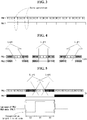
- FIG. 5 illustrates an example of a bad bright line appearing when a dark block adjacent to a bright block of the light valve panel PNL2 is turned on so as to prevent the color distortion of the side viewing angle.
- the bright block is disposed under a bright pixel (hereinafter, referred to as "ON-pixel") of the display panel PNL1 and means a block (hereinafter, referred to as "ON-block”) of the light valve panel PNL2 irradiating light onto the ON-pixel.
- the bright pixel is a pixel to which data of a high gray level, for example, a white gray level is applied.
- the dark block means a block (hereinafter, referred to as "OFF-block") of the light valve panel PNL2 disposed under a dark pixel (hereinafter, referred to as "OFF-pixel") adjacent to the ON-pixel of the display panel PNL1.
- the dark pixel is a pixel to which data of a low gray level, for example, a black gray level lower than the gray level of the ON-pixel is applied.
- OFF-block a block of the light valve panel PNL2 disposed under a dark pixel (hereinafter, referred to as "OFF-pixel") adjacent to the ON-pixel of the display panel PNL1.
- the dark pixel is a pixel to which data of a low gray level, for example, a black gray level lower than the gray level of the ON-pixel is applied.
- luminances of the OFF-blocks increase, luminances of the OFF-pixels may increase.
- luminances of the OFF-pixels at the front viewing angle may increase.
- the luminance of the OFF-pixel may be decreased using a modulation method for reducing a data value of the OFF-pixel adjacent to the ON-pixel.
- the modulation method may lead to the bright line phenomenon, in which a boundary between the OFF-pixel receiving data and the OFF-pixel receiving original data looks bright.
- the embodiment of the invention adjusts a luminance of the light valve panel PNL2 through a gradation method by distributing the voltage to the block in a manner that a luminance of the OFF-block adjacent to the ON-block in the light valve panel PNL2 gradually changes, so as to reduce the luminance and the color distortion at the side viewing angle and prevent the bright line phenomenon. Further, the embodiment of the invention may control a gray level of the OFF-pixel adjacent to the ON-pixel in reverse of a gradation luminance control method of the OFF-block.
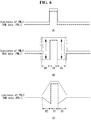
- FIG. 6 illustrates a pixel data modulation method of the display panel and a block luminance control method of the light valve panel.
- FIG. 7 illustrates a luminance of a pixel at a side viewing angle when data and a luminance of the display panel are controlled through a control method illustrated in (C) of FIG. 6 .
- D1 denotes a location of an ON-pixel and a location of an ON-block under the ON-pixel.
- D2 and D3 denote a location of an OFF-pixel and a location of an OFF-block under the OFF-pixel.
- FIG. 6 illustrates an example where data of a high gray level is applied only to an ON-pixel, and only an ON-block is turned on at a high luminance.
- (B) in FIG. 6 illustrates a method for increasing a luminance of an OFF-block adjacent to the ON-block by a luminance of the ON-block and reducing a gray level of data to be applied to an OFF-pixel adjacent to the ON-pixel, so as to improve a side viewing angle.
- FIG. 6 and FIG. 7 illustrate a method for gradually reducing a luminance of an OFF-block as the OFF-block is far away from the ON-block while increasing the luminance of the OFF-block adjacent to the ON-block by a luminance of the ON-block, so as to improve a side viewing angle and a bright line.
- Each block of the light valve panel PNL2 is disposed under pixels of the display panel PNL1 and irradiates light onto the pixels.
- there are OFF-pixels in the OFF-block adjacent to the ON-block and gray levels of the OFF-pixels can be individually adjusted as shown in (C) of FIG. 6 and FIG. 7 .
- the pixel data modulation method may use the gradation method shown in (C) of FIG.
- a luminance of the light valve panel PNL2 may use the gradation method of (C) in FIG. 6
- the pixel data modulation method may use the method shown in (B) or (C) of FIG. 6 .
- FIG. 8 is a cross-sectional view of a light valve panel.
- the light valve panel PNL 2 includes a second upper substrate 200 and a second lower substrate 210.
- the second upper substrate 200 includes a first base substrate 201 and a second electrode 203.
- the second electrode 203 may be formed of a transparent electrode material such as indium tin oxide (ITO).
- the second upper substrate 200 may include a black matrix (BM) if necessary.
- BM black matrix
- the second electrode 203 will be referred to as an upper electrode 203 in this specification.
- the second lower substrate 210 includes a second base substrate 211, an insulating layer 213, a light valve data line LVDL, and a first electrode 215.
- the first electrode 215 will be referred to as a lower electrode 215 in this specification.
- the lower electrode 215 may be formed of a transparent electrode material such as ITO.
- the lower electrode 215 is disposed over an entire surface of the light valve panel PNL2.
- the light valve data line LVDL is formed of a transparent electrode material such as indium tin oxide (ITO) and indium zinc oxide (IZO).
- ITO indium tin oxide
- IZO indium zinc oxide
- the light valve data line LVDL is preferably formed of a transparent electrode, so as to prevent the moire phenomenon but is not limited thereto.
- the light valve data line LVDL may be formed of a low resistance metal, so as to compensate for a resistance of the transparent electrode.
- the light valve data lines LVDL are connected to the lower electrode 215 to directly supply a light valve data voltage. Therefore, the light valve panel PNL2 does not need a TFT or a gate line (or a scan line) - so the PNL2 is a kind of passive matrix display.
- the embodiment of the invention can prevent a moire phenomenon and a bright line phenomenon and can further reduce the number of manufacturing processes of the light valve panel PNL2 by simplifying a structure of the light valve panel PNL2, thereby increasing a yield. Further, the embodiment of the invention omits a gate driving circuit for driving the light valve panel PNL2 and thus can implement a lower cost light valve panel PNL2.
- a polarizing film 24 is attached to the lower substrate 210 of the light valve panel PNL2.
- Alignment layers are respectively formed on surfaces contacting the liquid crystal layer at the upper substrate 200 and the lower substrate 210 of the light valve panel PNL2.
- a spacer for maintaining a cell gap of the liquid crystal cells may be formed between the upper substrate 200 and the lower substrate 210 of the light valve panel PNL2.
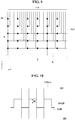
- FIG. 9 is a view illustrating block division of a light valve panel of the invention.
- the lower electrode of the light valve panel PNL2 includes an active area A/A and a bezel area Bezel. Arranged are M x N blocks BL in the active area A/A.
- the light valve data lines LVDL are parallel with each other and arranged in a vertical direction (a y-axis direction) in the active area A/A.
- Each of the light valve data lines LVDL is connected to blocks BL through a contact hole CNT.
- the light valve data voltage supplied to the lower electrode through the contact hole CNT is distributed to an area of the block BL.
- the light valve data lines LVDL are arranged vertically in parallel with a column direction (a y-axis direction) of the pixels P.
- FIG. 10 is a diagram illustrating a driving voltage of a light valve panel according to an embodiment of the invention.
- a polarity of a light valve data voltage LVData is inverted at regular intervals.
- a voltage higher than a reference common voltage RVCOM is defined as a positive polarity and a voltage lower than the reference common voltage RVCOM is defined as a negative polarity.
- a period in which the polarity of the light valve data voltage LVData is inverted may be synchronized with a polarity inversion period of a data voltage supplied to the pixel P of the display panel PNL1.
- a magnitude of the light valve data voltage LVData may be determined based on an image data and may be determined as a voltage level between a low potential voltage GND and a high potential voltage VDD.
- the reference common voltage RVCOM refers to an average value of the low potential voltage GND and the high potential voltage VDD in the light valve data voltage LVData.
- a period of a common voltage VCOM is synchronized with a period of the light valve data voltage LVData and the common voltage VCOM swings so as to have the same phase.
- a voltage higher than the reference common voltage RVCOM is defined as a positive polarity and a voltage lower than the reference common voltage RVCOM is defined as a negative polarity.
- the common voltage VCOM swings in a range between a positive voltage having a voltage level higher than the reference common voltage RVCOM by a modulation voltage MV and a negative voltage having a voltage level lower than the reference common voltage RVCOM by a modulation voltage MV.
- the common voltage VCOM applied to the upper electrode 203 swings with the same polarity as the light valve data voltage LVData applied to the lower electrode 215. Therefore, it is possible to improve an occurrence of image defects at a boundary of an image object displayed in white.
- FIG. 11 is a diagram illustrating TN mode characteristics for driving a liquid crystal layer 230 of a light valve panel PNL 2.
- FIG. 11 illustrates transmittance T of the liquid crystal layer 230 depending on a difference voltage V between the upper electrode 203 and the lower electrode 215.
- FIG. 12 is a diagram illustrating an example of a block image of a light valve panel.
- FIG. 13 is a graph illustrating a light valve data voltage and a reference common voltage according to a comparative example.
- FIG. 14 is a graph illustrating voltage distributions in blocks of the lower electrode to which a light valve data voltage shown in FIG. 13 is applied.
- a first to twelfth light valve data voltages LVData shown in FIG. 13 are voltages applied to a first to twelfth contact holes CNT1 to CNT12 located on I-I' in FIG. 12 .
- the reference common voltage RVCOM according to the comparative example shown in FIG. 13 is different from the common voltage VCOM according to the invention in that it maintains a constant voltage.
- FIG. 13 shows a positive light valve data voltage LVData in which a voltage level of the light valve data voltage LVData is larger than the reference common voltage RVCOM.
- a voltage equal to or close to a magnitude of the reference common voltage RVCOM is applied to the first to third contact holes CNT1 to CNT3 belonging to a block that displays white.
- a voltage equal to or close to the high potential voltage VDD is applied to the fifth to eighth contact holes CNT5 to CON8 belonging a block that displays black.
- the voltage applied through the light valve data line LVDL is distributed to the blocks BL of the lower electrode 215.
- the reference common voltage RVCOM which is the constant voltage shown in FIG. 10 , is applied to the upper electrode 203.
- FIG. 13 is an ideal voltage distribution of the lower electrode 215 located on I-I' of the light valve panel PNL2 by a voltage applied to the light valve data line LVDL.
- the voltage applied to the contact holes CNT is lowered due to a sheet resistance of the lower electrode 215, so that a voltage distribution of the lower electrode 215 located on I-I' appears as shown in FIG. 14 .
- the blocks BL that display white have a voltage higher than the voltage applied to the contact hole CNT toward the central area.
- the blocks BL that display black have a voltage lower than the voltage applied to the contact hole CNT toward the central area.
- the voltage distribution of the lower electrode 215 has voltage deviations ⁇ V1 and ⁇ V2 in comparison with the ideal voltage distribution excluding the sheet resistance.
- the blocks BL display different luminance due to the voltage deviations ⁇ V1 and ⁇ V2.
- the desired luminance can be displayed.
- the blocks BL display a black image.
- the blocks BL display a white image.
- the white margin WS is considerably narrower than the black margin BS, the white voltage deviation ⁇ V1 may deviate from the white margin WS.
- blocks BL displaying white at a position adjacent to a boundary between the white image and the black image have a larger voltage rise due to an influence of the high potential voltage VDD applied to the adjacent block BL.
- VDD high potential voltage
- an operation of securing the white margin WS of the light valve panel according to one embodiment of the present invention is as follows.
- FIG. 15 is a diagram illustrating a V-T characteristic curve of the TN mode when voltage amplitude of the common voltage VCOM is raised by the modulation voltage MV in comparison with the reference common voltage RVCOM.
- FIG.16 is a schematic diagram for explaining a principle of compensating a voltage drop of a lower electrode by a common voltage according to one embodiment of the invention.
- V-T characteristic curve of the invention is as follows.
- the common voltage VCOM has a value higher than the reference common voltage RVCOM by the modulation voltage MV.
- a voltage level of a block BL in which a difference voltage V from the reference common voltage RVCOM is V1 becomes a voltage level of the block BL in which a difference voltage V from the common voltage VCOM is V2.
- a difference voltage V in a first section A1 in which the difference voltage V is smaller than a magnitude of the modulation voltage MV becomes a negative(-) voltage.
- V-T characteristic curve for the positive light valve data voltage VLData belongs to a fourth section A4.
- the common voltage VCOM has a voltage lower than the reference common voltage RVCOM by the modulation voltage MV.
- a maximum value of the difference voltage V between the lower electrode 215 and the upper electrode 203 is a value obtained by adding the modulation voltage MV to the low potential voltage GND.
- a V-T characteristic curve of a fifth section A5 is excluded.
- a V-T characteristic curve for the negative light valve data voltage LVData belongs to a sixth section A6.
- the V-T characteristic curves by the positive light valve data voltage LVData and the negative light valve data voltage LVData belong to the fourth section A4 and the sixth section A6, respectively.
- the white margin WS is increased by the magnitude of the modulation voltage MV from the reference common voltage RVCOM.
- the white margin WS can be secured. As a result, it is possible to improve an occurrence of image defects in the block BL for displaying the white image due to insufficient white margin.
- the black margin BS decreases.
- the width of the black margin BS is considerably larger than the width of the white margin WS, it is rare that the difference voltage V deviates from the black margin BS even if the black margin BS decreases.
- the black image displayed by the block BL is distorted due to the deviation from the black margin BS, since the block BL is not visually perceptible, compensation conditions for widening the white margin WS are possible.
- a degree to which the white margin WS increases in the light valve panel PNL2 of the invention is proportional to the modulation voltage MV of the common voltage VCOM.
- the magnitude of the modulation voltage MV is the same as the difference from the reference common voltage RVCOM.
- the magnitude of the modulation voltage MV is set to such a degree that no inversion occurs in the white image display period.
- the magnitude of the modulation voltage MV is set to be equal to or less than the voltage width of the white margin in the V-T characteristic curve with reference to the reference common voltage RVCOM.
- the white margin can be calculated during a design process of the light valve panel, and the magnitude of the modulation voltage MV can be determined based on this.
Landscapes
- Physics & Mathematics (AREA)
- Engineering & Computer Science (AREA)
- General Physics & Mathematics (AREA)
- Nonlinear Science (AREA)
- Chemical & Material Sciences (AREA)
- Crystallography & Structural Chemistry (AREA)
- Theoretical Computer Science (AREA)
- Computer Hardware Design (AREA)
- Optics & Photonics (AREA)
- Mathematical Physics (AREA)
- Power Engineering (AREA)
- Geometry (AREA)
- Control Of Indicators Other Than Cathode Ray Tubes (AREA)
- Liquid Crystal Display Device Control (AREA)
- Liquid Crystal (AREA)
Abstract

Description
- The present disclosure relates to a liquid crystal display device that includes a control of an amount of light incident on a display panel based on a luminance distribution of an input image. Further it relates to a method for driving a light valve panel.
- Various flat panel displays, such as a liquid crystal display (LCD), an organic light emitting diode (OLED) display, a plasma display panel (PDP), and an electrophoretic display (EPD), have been developed. A liquid crystal display displays an image by controlling an electric field applied to liquid crystal molecules based on a data voltage. An active matrix liquid crystal display includes a thin film transistor (TFT) in each pixel.
- A liquid crystal display includes a display panel having a liquid crystal layer, a backlight unit irradiating light onto the display panel, a source driver integrated circuit (IC) for supplying a data voltage to data lines of the display panel, a gate driver IC for supplying gate pulses (or scan pulses) to gate lines (or scan lines) of the display panel, a control circuit for controlling the source driver IC and the gate driver IC, and a light source driving circuit for driving light sources of the backlight unit.
- Gray levels of an input image are produced by the data voltage applied to the pixels of the display panel. A liquid crystal display is not good in displaying a dark image due to the backlight. This is because the backlight unit irradiates a uniform amount of light onto the entire screen of the display panel regardless of a luminance distribution of the input image. Hence, the liquid crystal display has a limited contrast ratio.
- In one aspect, there is provided a light valve panel including a liquid crystal layer, a first electrode receiving a light valve data voltage through a light valve data line, and a second electrode facing the first electrode with the liquid crystal layer interposed therebetween, and receiving a common voltage swinging in the same phase in synchronization with the light valve data voltage.
- It is suggested that the light valve data voltage may swing between a positive voltage of a voltage level higher than a reference common voltage and a negative voltage of a voltage level lower than the reference common voltage.
- Preferably, the common voltage swings with a predetermined amplitude of a modulation voltage with reference to the reference common voltage.
- In particular, a magnitude of the modulation voltage is not larger than a white margin in a voltage-transmittance characteristic curve of the liquid crystal layer.
- It is further suggested that the second electrode is made of a single electrode layer and distributes the light valve data voltage applied through the light valve data line through a gradation method.
- Preferably, the light valve panel may include a second lower substrate and second upper substrate having the liquid crystal layer therebetween.
- It is suggested that the light valve panel drives liquid crystal molecules of the liquid crystal layer based on a difference between voltages applied to the second upper substrate and the second lower substrate.
- It is suggested that the light valve panel is a liquid crystal shutter that adjusts an amount of light in synchronization with an input image using electrically controlled liquid crystal molecules.
- It is suggested that the second lower substrate includes a second base substrate, the light valve data line disposed on the second base substrate and a first electrode.
- Preferably, the first electrode is formed of a transparent electrode material and is disposed over an entire surface of the light valve panel and/or the light valve data line is formed of a transparent electrode material.
- Preferably, the light valve data lines are connected to the first electrode to directly supply a light valve data voltage.
- Preferably, a diffuser sheet is disposed between the display panel and the light valve panel.
- In another aspect, there is provided a liquid crystal display device including a display panel on which pixels to which an input image is applied are arranged, a backlight unit irradiating light onto the display panel, and a light valve panel disposed between the display panel and the backlight unit, and which adjusts an amount of light from the backlight unit depending on the input image. The light valve panel includes a liquid crystal layer, a first electrode receiving a light valve data voltage through a light valve data line, and a second electrode facing the first electrode with the liquid crystal layer interposed therebetween, and receiving a common voltage swinging in the same phase in synchronization with the light valve data voltage.
- It is suggested that the display panel and the light valve panel are attached to each other by an adhesive.
- It is suggested that the light valve panel adjusts an amount of light to be irradiated onto the display panel.
- The accompanying drawings, which are included to provide a further understanding of the invention and are incorporated in and constitute a part of this specification, illustrate embodiments of the invention and together with the description serve to explain the principles of the invention. In the drawings:
-
FIG. 1 is a block diagram of a liquid crystal display according to an embodiment of the invention; -
FIG. 2 is a cross-sectional view illustrating a stack structure of a display panel, a light valve panel, and a backlight unit shown inFIG. 1 ; -
FIG. 3 illustrates moire appearing by an inference of light generated when metal lines of a display panel and metal lines of a light valve panel overlap each other; -
FIG. 4 illustrates a distortion of color generated by a gap between a display panel and a light valve panel; -
FIG. 5 illustrates an example of a bad bright line appearing when a dark block adjacent to a bright block in a light valve panel is turned on so as to prevent color distortion of a side viewing angle; -
FIG. 6 illustrates a pixel data modulation method of a display panel and a block luminance control method of a light valve panel; -
FIG. 7 illustrates a luminance of a pixel at a side viewing angle when data and a luminance of a display panel are controlled through a control method illustrated in (C) ofFIG. 6 ; -
FIG. 8 is a cross-sectional view of a light valve panel; -
FIG. 9 is a diagram illustrating block division of a light valve panel of the invention; -
FIG. 10 is a diagram illustrating a driving voltage of a light valve panel according to an embodiment of the invention; -
FIG. 11 is a diagram illustrating a V-T characteristic curve of a liquid crystal layer of a light valve panel; -
FIGS. 12 to 14 are diagrams illustrating a voltage drop phenomenon of a lower electrode in a block image display process; and -
FIGS. 15 to 16 are diagrams illustrating a process of securing a white margin by a common voltage of the invention. - Reference will now be made in example embodiments of the invention, of which are illustrated in the accompanying drawings. Wherever possible, the same reference numbers will be used throughout the drawings to refer to the same or like parts. It will be paid attention that detailed description of known arts will be omitted.
- Referring to
FIGS. 1 and 2 , a liquid crystal display according to an embodiment of the invention includes a display panel PNL1 including a pixel array, a backlight unit BLU irradiating light onto the display panel PNL1, a light valve panel PNL2 disposed between the display panel PNL1 and the backlight unit BLU, a firstpanel driving circuit panel driving circuit backlight driving circuit 40. - The display panel PNL1 includes a first
upper substrate 100 and a firstlower substrate 110, which are positioned opposite each other with a liquid crystal layer interposed therebetween. - On the first
upper substrate 100, a color filter array including black matrixes and color filters is formed. - On the first
lower substrate 110, data lines DL, gate lines GL,common electrodes 22,pixel electrodes 21 connected to TFTs, storage capacitors Cst connected to thepixel electrodes 21, and the like are formed. The TFTs are respectively formed in subpixels and are connected to thepixel electrodes 21. The TFTs may be implemented as an amorphous silicon (a-Si) TFT, a low temperature polysilicon (LTPS) TFT, an oxide TFT, and the like. The TFTs are respectively connected to thepixel electrodes 21 of the subpixels. Thecommon electrode 22 and thepixel electrode 21 are separated from each other with an insulating layer interposed therebetween. - The display panel PNL1 may be implemented in any known liquid crystal mode including a twisted nematic (TN) mode, a vertical alignment (VA) mode, an in-plane switching (IPS) mode, a fringe field switching (FFS) mode, etc.
- Polarizing
films upper substrate 100 and the firstlower substrate 110 of the display panel PNL1. Alignment layers for setting a pretilt angle of liquid crystals are respectively formed on the firstupper substrate 100 and the firstlower substrate 110 of the display panel PNL1. A spacer for maintaining a cell gap of liquid crystal cells Clc may be formed between the firstupper substrate 100 and the firstlower substrate 110 of the display panel PNL1. - The light valve panel PNL2 is disposed between the display panel PNL1 and the backlight unit BLU. The light valve panel PNL2 drives liquid crystal molecules based on a difference between voltages applied to a second
upper substrate 200 and a secondlower substrate 210 of the light valve panel PNL2 and adjusts an amount of light to be irradiated onto the display panel PNL1. The light valve panel PNL2 is a liquid crystal shutter that adjusts an amount of light in synchronization with an input image using electrically controlled liquid crystal molecules. - The liquid crystals of the light valve panel PNL2 may be driven in the TN mode. A luminance of the liquid crystal cell Clc in the TN mode may be adjusted depending on a transmittance-voltage curve (hereinafter, referred to as "T-V curve") of normally white. In the T-V curve of the normally white, as the voltage decreases, the transmittance increases. Hence, the luminance of the liquid crystal cell increases. On the contrary, as the voltage increase, the transmittance decreases. Hence, the luminance of the liquid crystal cell decreases. The structure and operation of the light valve panel PNL2 will be described later in detail.
- The display panel PNL1 and the light valve panel PNL2 may be attached to each other using an adhesive 23, for example, an optical clear adhesive (OCA).
- The first
panel driving circuit panel driving circuit first timing controller 10, afirst data driver 20, and agate driver 30. The firstpanel driving circuit - The
first timing controller 10 transmits digital video data of an input image received from ahost system 5 to thefirst data driver 20. Thefirst timing controller 10 receives timing signals synchronized with the data of the input image from thehost system 5. The timing signals include a vertical sync signal Vsync, a horizontal sync signal Hsync, a data enable signal DE, and a clock CLK, etc. Thefirst timing controller 10 controls operation timings of thefirst data driver 20 and thegate driver 30 based on the timing signals Vsync, Hsync, DE, and CLK received together with pixel data of the input image. Thefirst timing controller 10 may transmit a polarity control signal for controlling a polarity of the pixel array to each of source driver ICs of thefirst data driver 20. - Output channels of the
first data driver 20 are connected to the data lines DL of the pixel array. Thefirst data driver 20 receives the digital video data of the input image from thefirst timing controller 10. Thefirst data driver 20 converts the digital video data of the input image into positive and negative gamma compensation voltages under the control of thefirst timing controller 10 and outputs positive and negative data voltages. An output voltage of thefirst data driver 20 is supplied to the data lines DL. Thefirst data driver 20 inverts a polarity of the data voltage to be supplied to the pixels under the control of thefirst timing controller 10. - The
gate driver 30 sequentially supplies gate pulses synchronized with the data voltage to the gate lines GL under the control of thefirst timing controller 10. The gate pulses output from thegate driver 30 are synchronized with the data voltage supplied to the data lines DL. - The second
panel driving circuit panel driving circuit second timing controller 11 and asecond data driver 50. The secondpanel driving circuit - The
second timing controller 11 transmits data of an input image to thesecond data driver 50. Thesecond timing controller 11 receives timing signals synchronized with the data of the input image from thehost system 5. The timing signals include a vertical sync signal Vsync, a horizontal sync signal Hsync, a data enable signal DE, and a clock CLK, etc. Thesecond timing controller 11 controls operation timing of thesecond data driver 50 based on the timing signals Vsync, Hsync, DE, and CLK received together with pixel data of the input image. - The
second data driver 50 receives digital video data of an input image from thesecond timing controller 11. Thesecond data driver 50 converts the digital video data of the input image into positive and negative gamma compensation voltages under the control of thesecond timing controller 11 and outputs positive and negative data voltages. An output voltage of thesecond data driver 50 is supplied to data lines LVL. Thesecond data driver 50 inverts a polarity of the data voltage to be supplied to the pixels under the control ofsecond timing controller 11. - The first and second panel driving circuits may be integrated in various types. For example, the first and
second timing controllers - The backlight unit BLU may be implemented as a direct type backlight unit or an edge type backlight unit. The backlight unit BLU includes light sources LS, a light guide plate LGP, an optical sheet OPT, and the like. The light source LS may be implemented as a point light source such as a light emitting diode (LED). Luminances of the light sources LS are individually adjusted depending on a driving voltage supplied by a
backlight unit driver 40. The optical sheet OPT includes one or more prism sheets and one or more diffuser sheets. The optical sheet OPT diffuses light incident from the light guide plate LGP and refracts a travelling path of light at an angle substantially vertical to a light incident surface of the display panel PNL1. - The
host system 5 may be one of a television system, a set-top box, a navigation system, a DVD player, a Blu-ray player, a personal computer (PC), a home theater system, and a phone system. - The liquid crystal display according to the embodiment of the invention further includes a power unit. The power unit generates voltages required to drive the display panel PNL1 and the light valve panel PNL2 using a DC-DC converter. The voltages includes a high potential power voltage VDD, a logic power voltage VCC, a gamma reference voltage, a gate high voltage VGH, a gate low voltage VGL, a common voltage Vcom, and other voltages. The high potential power voltage VDD is a maximum value of the data voltage, to which pixels of the display panel PNL1 will be charged. The logic power voltage VCC is an IC power voltage of the first and second panel driving circuits. The gate high voltage VGH is a high logic voltage of the gate pulse, which is set to be equal to or greater than a threshold voltage of the TFTs of the pixel array. The gate low voltage VGL is a low logic voltage of the gate pulse, which is set to be less than the threshold voltage of the TFTs of the pixel array. The gate high voltage VGH and the gate low voltage VGL are supplied to the
gate driver 30. The gate pulse swings between the gate high voltage VGH and the gate low voltage VGL. The common voltage Vcom is supplied to thecommon electrode 22 of the liquid crystal cells Clc. The power unit divides the high potential power voltage VDD and generates the gamma reference voltage. The gamma reference voltage is divided by a voltage divider circuit installed inside thefirst data driver 20 and is divided into positive and negative gamma compensation voltages depending on a gray scale. - The light valve panel PNL2 precisely controls an amount of light irradiated onto each pixel in synchronization with data of an input image displayed on the pixel array and maximizes a contrast ratio of an image reproduced on the display panel PNL1. This is described with reference to
FIG. 3 . - Lines are formed on each of the display panel PNL1 and the light valve panel PNL2. The lines are not transparent and may be formed as metal lines having a high reflectance. The metal lines include data lines of a vertical direction, gate lines of a horizontal direction, and common lines of the horizontal direction. The common lines are connected to the common electrodes of the pixels and supply the common voltage Vcom to the common electrodes. Because the metal lines having the high reflectance lead to a reduction in the contrast ratio by reflecting external light, the metal lines and the TFTs are covered by a black matrix pattern. In this instance, when the lines of the display panel PNL1 overlap the lines of the light valve panel PNL2, the moire phenomenon may be generated in the vertical and horizontal directions due to interference of light if a misalignment is generated as shown in
FIG. 3 . In order to reduce the moire phenomenon, a diffuser sheet diffusing light may be disposed between the display panel PNL1 and the light valve panel PNL2. On the other hand, the embodiment of the invention removes the horizontal lines from the light valve panel PNL2 and forms the electrodes of the upper and lower substrates and the lines using a transparent electrode material, thereby minimizing the moire phenomenon without adding the diffuser sheet. - When a user watches the liquid crystal display at a front viewing angle, the user may watch an image at a desired luminance. However, when the user watches the liquid crystal display at a side viewing angle, a luminance and a color of the image may change. As shown in a middle diagram of
FIG. 4 , the front viewing angle is a viewing angle obtained when the user watches a display surface of the display panel PNL1 at an angle of 90°. The side viewing angle is a viewing angle obtained when the user watches the display surface of the display panel PNL1 at an angle leaned to the left side or the right side. InFIG. 4 , a left diagram is shown at a left viewing angle of 45°, and a right diagram is shown at a right viewing angle of 45°. In particular, because a predetermined gap ΔG is unconditionally formed between the display panel PNL1 and the light valve panel PNL2, color distortion of the liquid crystal display including the light valve panel PNL2 may more clearly appear at the side viewing angle. InFIG. 4 , only blocks of the light valve panel PNL2 positioned under pixels represented with white color transmit light, and other blocks of the light valve panel PNL2 block light. In this instance, when the user watches the liquid crystal display at the side viewing angle, luminances of some colors are reduced, and the color distortion appears. A method for adjusting a luminance of the light valve panel PNL2 shown inFIG. 5 may be considered, so as to improve the luminance of the side viewing angle. It should be noted that an example illustrated inFIG. 5 is not a related art. -
FIG. 5 illustrates an example of a bad bright line appearing when a dark block adjacent to a bright block of the light valve panel PNL2 is turned on so as to prevent the color distortion of the side viewing angle. The bright block is disposed under a bright pixel (hereinafter, referred to as "ON-pixel") of the display panel PNL1 and means a block (hereinafter, referred to as "ON-block") of the light valve panel PNL2 irradiating light onto the ON-pixel. The bright pixel is a pixel to which data of a high gray level, for example, a white gray level is applied. The dark block means a block (hereinafter, referred to as "OFF-block") of the light valve panel PNL2 disposed under a dark pixel (hereinafter, referred to as "OFF-pixel") adjacent to the ON-pixel of the display panel PNL1. The dark pixel is a pixel to which data of a low gray level, for example, a black gray level lower than the gray level of the ON-pixel is applied. As shown inFIG. 5 , when luminances of the OFF-blocks adjacent to the ON-block increase, each of red, green, and blue data at the side viewing angle can seen to have a desired luminance. Therefore, the color distortion at the side viewing angle can be reduced or prevented. On the other hand, when luminances of the OFF-blocks increase, luminances of the OFF-pixels may increase. Hence, luminances of the OFF-pixels at the front viewing angle may increase. In order to compensate for a reduction in image quality at the front viewing angle, the luminance of the OFF-pixel may be decreased using a modulation method for reducing a data value of the OFF-pixel adjacent to the ON-pixel. However, the modulation method may lead to the bright line phenomenon, in which a boundary between the OFF-pixel receiving data and the OFF-pixel receiving original data looks bright. - The embodiment of the invention adjusts a luminance of the light valve panel PNL2 through a gradation method by distributing the voltage to the block in a manner that a luminance of the OFF-block adjacent to the ON-block in the light valve panel PNL2 gradually changes, so as to reduce the luminance and the color distortion at the side viewing angle and prevent the bright line phenomenon. Further, the embodiment of the invention may control a gray level of the OFF-pixel adjacent to the ON-pixel in reverse of a gradation luminance control method of the OFF-block.
-
FIG. 6 illustrates a pixel data modulation method of the display panel and a block luminance control method of the light valve panel.FIG. 7 illustrates a luminance of a pixel at a side viewing angle when data and a luminance of the display panel are controlled through a control method illustrated in (C) ofFIG. 6 . - In
FIG. 6 , D1 denotes a location of an ON-pixel and a location of an ON-block under the ON-pixel. D2 and D3 denote a location of an OFF-pixel and a location of an OFF-block under the OFF-pixel. - (A) in
FIG. 6 illustrates an example where data of a high gray level is applied only to an ON-pixel, and only an ON-block is turned on at a high luminance. (B) inFIG. 6 illustrates a method for increasing a luminance of an OFF-block adjacent to the ON-block by a luminance of the ON-block and reducing a gray level of data to be applied to an OFF-pixel adjacent to the ON-pixel, so as to improve a side viewing angle. - (C) in
FIG. 6 andFIG. 7 illustrate a method for gradually reducing a luminance of an OFF-block as the OFF-block is far away from the ON-block while increasing the luminance of the OFF-block adjacent to the ON-block by a luminance of the ON-block, so as to improve a side viewing angle and a bright line. Each block of the light valve panel PNL2 is disposed under pixels of the display panel PNL1 and irradiates light onto the pixels. Thus, there are OFF-pixels in the OFF-block adjacent to the ON-block, and gray levels of the OFF-pixels can be individually adjusted as shown in (C) ofFIG. 6 andFIG. 7 . The pixel data modulation method may use the gradation method shown in (C) ofFIG. 6 . Other methods may be used. For example, a luminance of the light valve panel PNL2 may use the gradation method of (C) inFIG. 6 , and the pixel data modulation method may use the method shown in (B) or (C) ofFIG. 6 . -
FIG. 8 is a cross-sectional view of a light valve panel. - Referring to
FIG. 8 , the light valve panel PNL 2 includes a secondupper substrate 200 and a secondlower substrate 210. - The second
upper substrate 200 includes afirst base substrate 201 and asecond electrode 203. Thesecond electrode 203 may be formed of a transparent electrode material such as indium tin oxide (ITO). The secondupper substrate 200 may include a black matrix (BM) if necessary. Hereinafter, thesecond electrode 203 will be referred to as anupper electrode 203 in this specification. - The second
lower substrate 210 includes asecond base substrate 211, an insulating layer 213, a light valve data line LVDL, and afirst electrode 215. Hereinafter, thefirst electrode 215 will be referred to as alower electrode 215 in this specification. - The
lower electrode 215 may be formed of a transparent electrode material such as ITO. Thelower electrode 215 is disposed over an entire surface of the light valve panel PNL2. The light valve data line LVDL is formed of a transparent electrode material such as indium tin oxide (ITO) and indium zinc oxide (IZO). The light valve data line LVDL is preferably formed of a transparent electrode, so as to prevent the moire phenomenon but is not limited thereto. The light valve data line LVDL may be formed of a low resistance metal, so as to compensate for a resistance of the transparent electrode. - The light valve data lines LVDL are connected to the
lower electrode 215 to directly supply a light valve data voltage. Therefore, the light valve panel PNL2 does not need a TFT or a gate line (or a scan line) - so the PNL2 is a kind of passive matrix display. Hence, the embodiment of the invention can prevent a moire phenomenon and a bright line phenomenon and can further reduce the number of manufacturing processes of the light valve panel PNL2 by simplifying a structure of the light valve panel PNL2, thereby increasing a yield. Further, the embodiment of the invention omits a gate driving circuit for driving the light valve panel PNL2 and thus can implement a lower cost light valve panel PNL2. - A
polarizing film 24 is attached to thelower substrate 210 of the light valve panel PNL2. Alignment layers are respectively formed on surfaces contacting the liquid crystal layer at theupper substrate 200 and thelower substrate 210 of the light valve panel PNL2. A spacer for maintaining a cell gap of the liquid crystal cells may be formed between theupper substrate 200 and thelower substrate 210 of the light valve panel PNL2. -
FIG. 9 is a view illustrating block division of a light valve panel of the invention. - Referring to
FIGS. 8 and9 , the lower electrode of the light valve panel PNL2 includes an active area A/A and a bezel area Bezel. Arranged are M x N blocks BL in the active area A/A. - The light valve data lines LVDL are parallel with each other and arranged in a vertical direction (a y-axis direction) in the active area A/A. Each of the light valve data lines LVDL is connected to blocks BL through a contact hole CNT. The light valve data voltage supplied to the lower electrode through the contact hole CNT is distributed to an area of the block BL.
- The light valve data lines LVDL are arranged vertically in parallel with a column direction (a y-axis direction) of the pixels P.
-
FIG. 10 is a diagram illustrating a driving voltage of a light valve panel according to an embodiment of the invention. - Referring to
FIG. 10 , a polarity of a light valve data voltage LVData is inverted at regular intervals. Hereinafter, in the polarity of the light valve data voltage LVData of this specification, a voltage higher than a reference common voltage RVCOM is defined as a positive polarity and a voltage lower than the reference common voltage RVCOM is defined as a negative polarity. A period in which the polarity of the light valve data voltage LVData is inverted may be synchronized with a polarity inversion period of a data voltage supplied to the pixel P of the display panel PNL1. A magnitude of the light valve data voltage LVData may be determined based on an image data and may be determined as a voltage level between a low potential voltage GND and a high potential voltage VDD. - The reference common voltage RVCOM refers to an average value of the low potential voltage GND and the high potential voltage VDD in the light valve data voltage LVData.
- A period of a common voltage VCOM is synchronized with a period of the light valve data voltage LVData and the common voltage VCOM swings so as to have the same phase. In a polarity of the common voltage VCOM of this specification, a voltage higher than the reference common voltage RVCOM is defined as a positive polarity and a voltage lower than the reference common voltage RVCOM is defined as a negative polarity. The common voltage VCOM swings in a range between a positive voltage having a voltage level higher than the reference common voltage RVCOM by a modulation voltage MV and a negative voltage having a voltage level lower than the reference common voltage RVCOM by a modulation voltage MV.
- The common voltage VCOM applied to the
upper electrode 203 swings with the same polarity as the light valve data voltage LVData applied to thelower electrode 215. Therefore, it is possible to improve an occurrence of image defects at a boundary of an image object displayed in white. - An embodiment of the invention will be described in addition to a comparative example in which the common voltage VCOM of a constant voltage is applied.
-
FIG. 11 is a diagram illustrating TN mode characteristics for driving aliquid crystal layer 230 of a light valve panel PNL 2.FIG. 11 illustrates transmittance T of theliquid crystal layer 230 depending on a difference voltage V between theupper electrode 203 and thelower electrode 215. - Referring to
FIG. 11 , in a normally white V-T curve, as the voltage difference between theupper electrode 203 and thelower electrode 215 is small, the transmittance becomes higher and the luminance of the light valve panel PNL2 becomes higher. As the voltage difference between theupper electrode 203 and thelower electrode 215 is large, the transmittance becomes lower and the luminance of the light valve panel PNL2 becomes lower. When the voltage difference between theupper electrode 203 and thelower electrode 215 belongs to a white margin WS, the light valve panel PNL2 displays white. When the voltage difference between theupper electrode 203 and thelower electrode 215 belongs to a black margin BS, the light valve panel PNL2 displays black. -
FIG. 12 is a diagram illustrating an example of a block image of a light valve panel.FIG. 13 is a graph illustrating a light valve data voltage and a reference common voltage according to a comparative example.FIG. 14 is a graph illustrating voltage distributions in blocks of the lower electrode to which a light valve data voltage shown inFIG. 13 is applied. A first to twelfth light valve data voltages LVData shown inFIG. 13 are voltages applied to a first to twelfth contact holes CNT1 to CNT12 located on I-I' inFIG. 12 . The reference common voltage RVCOM according to the comparative example shown inFIG. 13 is different from the common voltage VCOM according to the invention in that it maintains a constant voltage.FIG. 13 shows a positive light valve data voltage LVData in which a voltage level of the light valve data voltage LVData is larger than the reference common voltage RVCOM. - In a process of displaying the pattern image as shown in
FIG. 12 by the light valve panel PNL2 operating in the TN mode, a comparative example in which a constant voltage is applied to the upper electrode will be described below. - Referring to
FIGS. 12 and13 , a voltage equal to or close to a magnitude of the reference common voltage RVCOM is applied to the first to third contact holes CNT1 to CNT3 belonging to a block that displays white. A voltage equal to or close to the high potential voltage VDD is applied to the fifth to eighth contact holes CNT5 to CON8 belonging a block that displays black. The voltage applied through the light valve data line LVDL is distributed to the blocks BL of thelower electrode 215. - The reference common voltage RVCOM, which is the constant voltage shown in
FIG. 10 , is applied to theupper electrode 203. -
FIG. 13 is an ideal voltage distribution of thelower electrode 215 located on I-I' of the light valve panel PNL2 by a voltage applied to the light valve data line LVDL. However, the voltage applied to the contact holes CNT is lowered due to a sheet resistance of thelower electrode 215, so that a voltage distribution of thelower electrode 215 located on I-I' appears as shown inFIG. 14 . As a result, as shown inFIG. 14 , the blocks BL that display white have a voltage higher than the voltage applied to the contact hole CNT toward the central area. The blocks BL that display black have a voltage lower than the voltage applied to the contact hole CNT toward the central area. The voltage distribution of thelower electrode 215 has voltage deviations ΔV1 and ΔV2 in comparison with the ideal voltage distribution excluding the sheet resistance. - The blocks BL display different luminance due to the voltage deviations ΔV1 and ΔV2. However, when the voltage deviations ΔV1 and ΔV2 belong to the white margin WS or the black margin BS, the desired luminance can be displayed. For example, when a black voltage deviation ΔV2 belongs to the black margin BS shown in
FIG. 11 , the blocks BL display a black image. Further, when a white voltage deviation ΔV1 belongs to the white margin WS shown inFIG. 11 , the blocks BL display a white image. - As shown in
FIG. 11 , since the V-T curve of the TN mode has a relatively large black margin BS, even if the black voltage deviation ΔV2 occurs as shown inFIG. 14 , an image distortion does not occur and blocks BL can display black. - However, since the white margin WS is considerably narrower than the black margin BS, the white voltage deviation ΔV1 may deviate from the white margin WS. In particular, as shown in
FIG. 12 , blocks BL displaying white at a position adjacent to a boundary between the white image and the black image have a larger voltage rise due to an influence of the high potential voltage VDD applied to the adjacent block BL. As a result, there is a problem that the blocks BL, which should display white, display gray. - In contrast to this comparative example, an operation of securing the white margin WS of the light valve panel according to one embodiment of the present invention is as follows.
-
FIG. 15 is a diagram illustrating a V-T characteristic curve of the TN mode when voltage amplitude of the common voltage VCOM is raised by the modulation voltage MV in comparison with the reference common voltage RVCOM.FIG.16 is a schematic diagram for explaining a principle of compensating a voltage drop of a lower electrode by a common voltage according to one embodiment of the invention. - Referring to
FIGS. 15 and16 , the V-T characteristic curve of the invention is as follows. - When the light valve data voltage LVData is positive, the common voltage VCOM has a value higher than the reference common voltage RVCOM by the modulation voltage MV.
- When the voltage of the
upper electrode 203 becomes high, the voltage difference between thelower electrode 215 and theupper electrode 203 becomes smaller, and a section of the V-T characteristic curve is shifted to the left direction. For example, as shown inFIG. 16 , a voltage level of a block BL in which a difference voltage V from the reference common voltage RVCOM is V1 becomes a voltage level of the block BL in which a difference voltage V from the common voltage VCOM is V2. When the common voltage VCOM rises by the modulation voltage MV, in the V-T characteristic curve with reference to the reference common voltage RVCOM, a difference voltage V in a first section A1 in which the difference voltage V is smaller than a magnitude of the modulation voltage MV becomes a negative(-) voltage. As a result, when the voltage of theupper electrode 203 rises by the magnitude of the modulation voltage MV, a V-T characteristic curve belonging to the first section A1 in thelower electrode 215 belongs to a V-T characteristic curve belonging to a second section A2. That is, when the difference voltage V is V1, image distortion may occur due to deviation from the white margin WS. However, when the common voltage VCOM rises as in the invention, image distortion does not occur because it belongs to a white margin range of an opposite polarity area. - When the voltage of the
upper electrode 203 rises by the magnitude of the modulation voltage MV, a maximum value of the difference voltage V between thelower electrode 215 and theupper electrode 203 becomes a value obtained by subtracting the modulation voltage MV from the high potential voltage VDD. As a result, when the voltage of theupper electrode 203 rises by the magnitude of the modulation voltage MV, a V-T characteristic curve of a third section A3 is excluded. - As a result, when the voltage of the
upper electrode 203 rises by the magnitude of the modulation voltage MV, a V-T characteristic curve for the positive light valve data voltage VLData belongs to a fourth section A4. - When the light valve data voltage LVData is negative, the common voltage VCOM has a voltage lower than the reference common voltage RVCOM by the modulation voltage MV.
- When the voltage of the
upper electrode 203 is lowered, as the voltage difference between thelower electrode 215 and theupper electrode 203 becomes smaller, a section of the V-T characteristic curve is shifted to the right direction. In particular, when the common voltage VCOM is lowered by the modulation voltage MV, in the V-T characteristic curve with reference to the reference common voltage RVCOM, a difference voltage V of the second section A2 in which the difference voltage V is smaller than the magnitude of the modulation voltage MV becomes a positive(+) voltage. As a result, when the voltage of theupper electrode 203 is lowered by the magnitude of the modulation voltage MV, a V-T characteristic curve belonging to the second section A2 in thelower electrode 215 belongs to a V-T characteristic curve belonging to the first section A1. - When the voltage of the
upper electrode 203 is a value smaller by the magnitude of the modulation voltage MV, a maximum value of the difference voltage V between thelower electrode 215 and theupper electrode 203 is a value obtained by adding the modulation voltage MV to the low potential voltage GND. As a result, when the voltage of theupper electrode 203 falls by the magnitude of the modulation voltage MV, a V-T characteristic curve of a fifth section A5 is excluded. - As a result, when the voltage of the
upper electrode 203 falls by the magnitude of the modulation voltage MV, a V-T characteristic curve for the negative light valve data voltage LVData belongs to a sixth section A6. - As a result, the V-T characteristic curves by the positive light valve data voltage LVData and the negative light valve data voltage LVData belong to the fourth section A4 and the sixth section A6, respectively. The white margin WS is increased by the magnitude of the modulation voltage MV from the reference common voltage RVCOM. In the light valve panel PNL2 of the invention, since the common voltage VCOM swings in the same phase as the light valve data voltage LVData, the white margin WS can be secured. As a result, it is possible to improve an occurrence of image defects in the block BL for displaying the white image due to insufficient white margin.
- Meanwhile, in the light valve data voltage LVData of the invention, the black margin BS decreases. However, since the width of the black margin BS is considerably larger than the width of the white margin WS, it is rare that the difference voltage V deviates from the black margin BS even if the black margin BS decreases. Further, even if the black image displayed by the block BL is distorted due to the deviation from the black margin BS, since the block BL is not visually perceptible, compensation conditions for widening the white margin WS are possible.
- A degree to which the white margin WS increases in the light valve panel PNL2 of the invention is proportional to the modulation voltage MV of the common voltage VCOM. The magnitude of the modulation voltage MV is the same as the difference from the reference common voltage RVCOM. The magnitude of the modulation voltage MV is set to such a degree that no inversion occurs in the white image display period. When the magnitude of the modulation voltage MV is larger than the voltage level width of the white margin, it is deviated from the white margin in the opposite polarity area of the V-T characteristic curve. Therefore, the magnitude of the modulation voltage MV is set to be equal to or less than the voltage width of the white margin in the V-T characteristic curve with reference to the reference common voltage RVCOM. The white margin can be calculated during a design process of the light valve panel, and the magnitude of the modulation voltage MV can be determined based on this.
- Although embodiments have been described with reference to a number of illustrative embodiments thereof, it should be understood that numerous other modifications and embodiments can be devised by those skilled in the art that will fall within the scope of the principles of this disclosure. More particularly, various variations and modifications are possible in the component parts and/or arrangements of the subject combination arrangement within the scope of the disclosure, the drawings and the appended claims. In addition to variations and modifications in the component parts and/or arrangements, alternative uses will also be apparent to those skilled in the art.
Claims (15)
- A light valve panel (PNL2) comprising:a liquid crystal layer (230);a first electrode (215) receiving a light valve data voltage (LVData) through a light valve data line (LVDL); anda second electrode (203) facing the first electrode (215) with the liquid crystal layer (230) interposed therebetween, and receiving a common voltage (Vcom) swinging in the same phase in synchronization with the light valve data voltage (LVData).
- The light valve panel of claim 1, wherein the light valve data voltage (LVData) swings between a positive voltage of a voltage level higher than a reference common voltage (RVCOM) and a negative voltage of a voltage level lower than the reference common voltage (RVCOM), and
wherein the common voltage (VCOM) swings with a predetermined amplitude of a modulation voltage (MV) with reference to the reference common voltage (RVCOM). - The light valve panel of claim 2, wherein a magnitude of the modulation voltage (MV) is not larger than a white margin (WS) in a voltage-transmittance (V-T) characteristic curve of the liquid crystal layer (230).
- The light valve panel as claimed in any one of the preceding claims, wherein the second electrode (203) is made of a single electrode layer and distributes the light valve data voltage (LVData) applied through the light valve data line (LVDL) through a gradation method.
- The light valve panel as claimed in any one of the preceding claims, wherein the light valve panel (PNL2) includes a second lower substrate (210) and second upper substrate (200) having the the liquid crystal layer (230) therebetween.
- The light valve panel as claimed in claim 5, wherein the light valve panel (PNL2) drives liquid crystal molecules of the liquid crystal layer (230) based on a difference between voltages applied to the second upper substrate (200) and the second lower substrate (210).
- The light valve panel as claimed in any one of the preceding claims, wherein the light valve panel (PNL2) is a liquid crystal shutter that adjusts an amount of light in synchronization with an input image using electrically controlled liquid crystal molecules.
- The light valve panel as claimed in any one of the preceding claims, wherein the second lower substrate (210) includes a second base substrate (211), the light valve data line (LVDL) disposed on the second base substrate (211) and a first electrode (215).
- The light valve panel as claimed in claim 8, wherein the first electrode (215) is formed of a transparent electrode material and is disposed over an entire surface of the light valve panel (PNL2) and/or the light valve data line (LVDL) is formed of a transparent electrode material.
- The light valve panel as claimed in claim 9, wherein the light valve data lines (LVDL) are connected to the first electrode (215) to directly supply a light valve data voltage (LVData).
- The light valve panel as claimed in any one of the preceding claims, wherein a diffuser sheet is disposed between the display panel (PNL1) and the light valve panel (PNL2).
- A liquid crystal display device comprising:a display panel (PNL1) on which pixels to which an input image is applied are arranged;a backlight unit (BLU) irradiating light onto the display panel (PNL1); anda light valve panel (PNL2) as claimed in any one of the claims 1-11, disposed between the display panel (PNL1) and the backlight unit (BLU), for adjusting an amount of light from the backlight unit (BLU) depending on the input image.
- The liquid crystal display device of claim 12, wherein the display panel (PNL1) and the light valve panel (PNL2) are attached to each other by an adhesive (23).
- The light valve panel as claimed in claim 12 or 13, wherein the light valve panel (PNL2) adjusts an amount of light to be irradiated onto the display panel (PNL1).
- Method for controlling an amount of light irradiated onto the display panel (PNL1) by a back light unit (BLU), wherein a light valve panel (PNL2) as claimed in any one of the claims 1-11, disposed between the display panel (PNL1) and the backlight unit (BLU), for adjusting an amount of light from the backlight unit (BLU) depending on the input image, comprising the steps of:analysing an input image;providing a light valve data voltage (LVData) through a light valve data line (LVDL) to the first electrode (215) depending on the input image; andproviding a common voltage (Vcom) to a second electrode (203) of the light valve panel (PNL2) swinging in the same phase in synchronization with the light valve data voltage (LVData).
Applications Claiming Priority (1)
| Application Number | Priority Date | Filing Date | Title |
|---|---|---|---|
| KR1020160067778A KR102541940B1 (en) | 2016-05-31 | 2016-05-31 | Light valve panel and liquid crystal display device using the same |
Publications (3)
| Publication Number | Publication Date |
|---|---|
| EP3252752A2 true EP3252752A2 (en) | 2017-12-06 |
| EP3252752A3 EP3252752A3 (en) | 2018-03-21 |
| EP3252752B1 EP3252752B1 (en) | 2020-07-01 |
Family
ID=58873684
Family Applications (1)
| Application Number | Title | Priority Date | Filing Date |
|---|---|---|---|
| EP17173485.8A Active EP3252752B1 (en) | 2016-05-31 | 2017-05-30 | Light valve panel and liquid crystal display using the same |
Country Status (4)
| Country | Link |
|---|---|
| US (1) | US10490138B2 (en) |
| EP (1) | EP3252752B1 (en) |
| KR (1) | KR102541940B1 (en) |
| CN (1) | CN107450203B (en) |
Cited By (1)
| Publication number | Priority date | Publication date | Assignee | Title |
|---|---|---|---|---|
| US11988931B2 (en) | 2020-10-19 | 2024-05-21 | Hefei Boe Optoelectronics Technology Co., Ltd. | Display module and manufacturing method therefor, and display device |
Families Citing this family (21)
| Publication number | Priority date | Publication date | Assignee | Title |
|---|---|---|---|---|
| JP6873785B2 (en) * | 2017-03-30 | 2021-05-19 | パナソニック液晶ディスプレイ株式会社 | Liquid crystal display device |
| CN107908042A (en) * | 2017-12-28 | 2018-04-13 | 惠州市华星光电技术有限公司 | Liquid crystal module and liquid crystal display device |
| CN108227320A (en) * | 2018-03-07 | 2018-06-29 | 京东方科技集团股份有限公司 | Display device |
| CN110320723B (en) * | 2018-03-28 | 2023-12-19 | 京东方科技集团股份有限公司 | Display device, display method and display device thereof |
| JP7306383B2 (en) * | 2018-05-22 | 2023-07-11 | ソニーグループ株式会社 | Image processing device, display device, image processing method |
| JP2020056807A (en) * | 2018-09-28 | 2020-04-09 | 株式会社ジャパンディスプレイ | Display |
| JP2020052363A (en) * | 2018-09-28 | 2020-04-02 | 株式会社ジャパンディスプレイ | Display device |
| KR102592143B1 (en) * | 2019-02-22 | 2023-10-23 | 삼성전자주식회사 | Display apparatus and method for driving thereof |
| CN109870859A (en) * | 2019-03-19 | 2019-06-11 | 京东方科技集团股份有限公司 | A kind of display panel and its manufacturing method, display device |
| CN111785222B (en) * | 2019-04-04 | 2021-05-28 | 海信视像科技股份有限公司 | A contrast enhancement algorithm and dual-panel display device |
| US11263987B2 (en) | 2019-04-04 | 2022-03-01 | Hisense Visual Technology Co., Ltd. | Method of enhancing contrast and a dual-cell display apparatus |
| US11004406B1 (en) * | 2020-01-05 | 2021-05-11 | Himax Technologies Limited | Dual liquid crystal display device |
| CN113936614B (en) * | 2020-06-29 | 2022-10-04 | 京东方科技集团股份有限公司 | Driving method and driving device for display panel, display device and storage medium |
| TWI737420B (en) | 2020-07-27 | 2021-08-21 | 友達光電股份有限公司 | Display apparatus |
| KR20220030574A (en) * | 2020-09-03 | 2022-03-11 | 엘지이노텍 주식회사 | Light route control member and display having the same |
| CN114442385A (en) * | 2020-10-30 | 2022-05-06 | 京东方科技集团股份有限公司 | Display module, display device and control method of display device |
| WO2022099554A1 (en) * | 2020-11-12 | 2022-05-19 | 京东方科技集团股份有限公司 | Display method, display device, and storage medium |
| JP7555303B2 (en) * | 2021-05-21 | 2024-09-24 | 株式会社ジャパンディスプレイ | Display device |
| JP2023000471A (en) * | 2021-06-18 | 2023-01-04 | シャープディスプレイテクノロジー株式会社 | Liquid crystal display device |
| JP7634459B2 (en) * | 2021-10-08 | 2025-02-21 | 株式会社ジャパンディスプレイ | Display device |
| CN115241351B (en) * | 2022-06-15 | 2026-03-20 | Tcl华星光电技术有限公司 | Display panel |
Family Cites Families (20)
| Publication number | Priority date | Publication date | Assignee | Title |
|---|---|---|---|---|
| CN1220098C (en) | 2000-04-28 | 2005-09-21 | 夏普株式会社 | Display device, display device driving method, and electronic equipment incorporating display device |
| KR100698048B1 (en) * | 2003-06-26 | 2007-03-23 | 엘지.필립스 엘시디 주식회사 | LCD Display |
| JP5176194B2 (en) * | 2006-04-18 | 2013-04-03 | Nltテクノロジー株式会社 | Liquid crystal display device and image display system |
| US7916223B2 (en) * | 2006-04-18 | 2011-03-29 | Nec Lcd Technologies, Ltd. | Dual panel liquid crystal display device |
| TWI339375B (en) * | 2007-01-29 | 2011-03-21 | Chimei Innolux Corp | Liquid crystal display device and driving method using the same |
| JP5235363B2 (en) * | 2007-09-04 | 2013-07-10 | 株式会社ジャパンディスプレイイースト | Liquid crystal display |
| KR20090050857A (en) | 2007-11-16 | 2009-05-20 | 삼성모바일디스플레이주식회사 | LCD and its driving method |
| KR101508719B1 (en) * | 2008-10-06 | 2015-04-03 | 삼성디스플레이 주식회사 | Drive unit and display device having the same |
| US9864243B2 (en) * | 2010-05-14 | 2018-01-09 | Dolby Laboratories Licensing Corporation | High dynamic range displays using filterless LCD(s) for increasing contrast and resolution |
| TWI518652B (en) * | 2010-10-20 | 2016-01-21 | 達意科技股份有限公司 | Electro-phoretic display apparatus |
| JP2015049426A (en) * | 2013-09-03 | 2015-03-16 | パナソニック液晶ディスプレイ株式会社 | Liquid crystal display |
| JP2016038567A (en) | 2014-08-08 | 2016-03-22 | キヤノン株式会社 | Display device and control method thereof |
| JP2016071337A (en) * | 2014-09-29 | 2016-05-09 | 株式会社ジャパンディスプレイ | Display device |
| US9753596B2 (en) * | 2014-09-29 | 2017-09-05 | Japan Display Inc. | Display device with display of complementary portion between dark portion and bright portion |
| KR102440113B1 (en) * | 2015-01-02 | 2022-09-05 | 삼성디스플레이 주식회사 | Optical modulatoin device |
| CN105068695A (en) * | 2015-09-11 | 2015-11-18 | 京东方科技集团股份有限公司 | Touch display panel with pressure detection function, display device and driving method |
| KR20170049701A (en) * | 2015-10-27 | 2017-05-11 | 삼성디스플레이 주식회사 | Display apparatus and method of operating the same |
| CN105372884A (en) * | 2015-12-02 | 2016-03-02 | 武汉华星光电技术有限公司 | LCD panel and electronic device using same |
| JP6560610B2 (en) * | 2015-12-18 | 2019-08-14 | 株式会社ジャパンディスプレイ | Display device |
| JP2017167403A (en) * | 2016-03-17 | 2017-09-21 | 株式会社ジャパンディスプレイ | Display device |
-
2016
- 2016-05-31 KR KR1020160067778A patent/KR102541940B1/en active Active
-
2017
- 2017-05-25 US US15/604,929 patent/US10490138B2/en active Active
- 2017-05-27 CN CN201710391744.4A patent/CN107450203B/en active Active
- 2017-05-30 EP EP17173485.8A patent/EP3252752B1/en active Active
Non-Patent Citations (1)
| Title |
|---|
| None |
Cited By (1)
| Publication number | Priority date | Publication date | Assignee | Title |
|---|---|---|---|---|
| US11988931B2 (en) | 2020-10-19 | 2024-05-21 | Hefei Boe Optoelectronics Technology Co., Ltd. | Display module and manufacturing method therefor, and display device |
Also Published As
| Publication number | Publication date |
|---|---|
| CN107450203A (en) | 2017-12-08 |
| EP3252752B1 (en) | 2020-07-01 |
| CN107450203B (en) | 2020-09-18 |
| EP3252752A3 (en) | 2018-03-21 |
| KR20170136151A (en) | 2017-12-11 |
| US10490138B2 (en) | 2019-11-26 |
| KR102541940B1 (en) | 2023-06-12 |
| US20170343839A1 (en) | 2017-11-30 |
Similar Documents
| Publication | Publication Date | Title |
|---|---|---|
| EP3252752B1 (en) | Light valve panel and liquid crystal display using the same | |
| US10109241B2 (en) | Light valve panel and liquid crystal display using the same | |
| US10303019B2 (en) | Light valve panel and liquid crystal display using the same | |
| US9182805B2 (en) | Display device and method to control driving voltages based on changes in display image frame frequency | |
| US8289310B2 (en) | Horizontal electric field liquid crystal display | |
| JPWO2010143348A1 (en) | Liquid crystal display | |
| KR101613734B1 (en) | Liquid Crystal Display | |
| US12518714B2 (en) | Liquid crystal display drive device and method of driving the same, and image processor | |
| US20230335076A1 (en) | Lcd panel, driving method and display device | |
| KR20180002967A (en) | Light valve panel and liquid crystal display device using the same | |
| KR20210026274A (en) | Backlight Unit and Liquid Crystal Display Device using the same | |
| US8902143B2 (en) | Liquid crystal display for driving a pixel with a black state and a white state within one frame period, method of driving the same and electronic unit including the same | |
| US9508298B2 (en) | Adaptive inversion control of liquid crystal display device | |
| KR102013378B1 (en) | Liquid crystal display | |
| KR100538330B1 (en) | Liquid crystal display and driving method thereof | |
| KR102253321B1 (en) | Liquid crystal display and method for driving the same | |
| KR20110036209A (en) | LCD and Local Dimming Control Method | |
| KR20120002190A (en) | LCD and its driving method | |
| KR20170015819A (en) | Light valve panel and liquid crystal display device using the same |
Legal Events
| Date | Code | Title | Description |
|---|---|---|---|
| PUAI | Public reference made under article 153(3) epc to a published international application that has entered the european phase |
Free format text: ORIGINAL CODE: 0009012 |
|
| STAA | Information on the status of an ep patent application or granted ep patent |
Free format text: STATUS: REQUEST FOR EXAMINATION WAS MADE |
|
| 17P | Request for examination filed |
Effective date: 20170530 |
|
| AK | Designated contracting states |
Kind code of ref document: A2 Designated state(s): AL AT BE BG CH CY CZ DE DK EE ES FI FR GB GR HR HU IE IS IT LI LT LU LV MC MK MT NL NO PL PT RO RS SE SI SK SM TR |
|
| AX | Request for extension of the european patent |
Extension state: BA ME |
|
| PUAL | Search report despatched |
Free format text: ORIGINAL CODE: 0009013 |
|
| AK | Designated contracting states |
Kind code of ref document: A3 Designated state(s): AL AT BE BG CH CY CZ DE DK EE ES FI FR GB GR HR HU IE IS IT LI LT LU LV MC MK MT NL NO PL PT RO RS SE SI SK SM TR |
|
| AX | Request for extension of the european patent |
Extension state: BA ME |
|
| RIC1 | Information provided on ipc code assigned before grant |
Ipc: G09G 3/34 20060101AFI20180210BHEP Ipc: G09G 3/36 20060101ALI20180210BHEP Ipc: G02F 1/1347 20060101ALI20180210BHEP |
|
| RBV | Designated contracting states (corrected) |
Designated state(s): AL AT BE BG CH CY CZ DE DK EE ES FI FR GB GR HR HU IE IS IT LI LT LU LV MC MK MT NL NO PL PT RO RS SE SI SK SM TR |
|
| STAA | Information on the status of an ep patent application or granted ep patent |
Free format text: STATUS: EXAMINATION IS IN PROGRESS |
|
| 17Q | First examination report despatched |
Effective date: 20181030 |
|
| GRAP | Despatch of communication of intention to grant a patent |
Free format text: ORIGINAL CODE: EPIDOSNIGR1 |
|
| STAA | Information on the status of an ep patent application or granted ep patent |
Free format text: STATUS: GRANT OF PATENT IS INTENDED |
|
| INTG | Intention to grant announced |
Effective date: 20200108 |
|
| RAP1 | Party data changed (applicant data changed or rights of an application transferred) |
Owner name: LG DISPLAY CO., LTD. |
|
| RIN1 | Information on inventor provided before grant (corrected) |
Inventor name: YOO, OOKSANG Inventor name: KIM, KYUJIN Inventor name: YOO, SEUNGJIN Inventor name: NAM, SANGJIN |
|
| GRAS | Grant fee paid |
Free format text: ORIGINAL CODE: EPIDOSNIGR3 |
|
| GRAA | (expected) grant |
Free format text: ORIGINAL CODE: 0009210 |
|
| STAA | Information on the status of an ep patent application or granted ep patent |
Free format text: STATUS: THE PATENT HAS BEEN GRANTED |
|
| AK | Designated contracting states |
Kind code of ref document: B1 Designated state(s): AL AT BE BG CH CY CZ DE DK EE ES FI FR GB GR HR HU IE IS IT LI LT LU LV MC MK MT NL NO PL PT RO RS SE SI SK SM TR |
|
| REG | Reference to a national code |
Ref country code: CH Ref legal event code: EP Ref country code: AT Ref legal event code: REF Ref document number: 1286900 Country of ref document: AT Kind code of ref document: T Effective date: 20200715 |
|
| REG | Reference to a national code |
Ref country code: IE Ref legal event code: FG4D |
|
| REG | Reference to a national code |
Ref country code: DE Ref legal event code: R096 Ref document number: 602017018906 Country of ref document: DE |
|
| REG | Reference to a national code |
Ref country code: LT Ref legal event code: MG4D |
|
| PG25 | Lapsed in a contracting state [announced via postgrant information from national office to epo] |
Ref country code: BG Free format text: LAPSE BECAUSE OF FAILURE TO SUBMIT A TRANSLATION OF THE DESCRIPTION OR TO PAY THE FEE WITHIN THE PRESCRIBED TIME-LIMIT Effective date: 20201001 |
|
| REG | Reference to a national code |
Ref country code: NL Ref legal event code: MP Effective date: 20200701 |
|
| REG | Reference to a national code |
Ref country code: AT Ref legal event code: MK05 Ref document number: 1286900 Country of ref document: AT Kind code of ref document: T Effective date: 20200701 |
|
| PG25 | Lapsed in a contracting state [announced via postgrant information from national office to epo] |
Ref country code: PT Free format text: LAPSE BECAUSE OF FAILURE TO SUBMIT A TRANSLATION OF THE DESCRIPTION OR TO PAY THE FEE WITHIN THE PRESCRIBED TIME-LIMIT Effective date: 20201102 Ref country code: AT Free format text: LAPSE BECAUSE OF FAILURE TO SUBMIT A TRANSLATION OF THE DESCRIPTION OR TO PAY THE FEE WITHIN THE PRESCRIBED TIME-LIMIT Effective date: 20200701 Ref country code: HR Free format text: LAPSE BECAUSE OF FAILURE TO SUBMIT A TRANSLATION OF THE DESCRIPTION OR TO PAY THE FEE WITHIN THE PRESCRIBED TIME-LIMIT Effective date: 20200701 Ref country code: LT Free format text: LAPSE BECAUSE OF FAILURE TO SUBMIT A TRANSLATION OF THE DESCRIPTION OR TO PAY THE FEE WITHIN THE PRESCRIBED TIME-LIMIT Effective date: 20200701 Ref country code: GR Free format text: LAPSE BECAUSE OF FAILURE TO SUBMIT A TRANSLATION OF THE DESCRIPTION OR TO PAY THE FEE WITHIN THE PRESCRIBED TIME-LIMIT Effective date: 20201002 Ref country code: NO Free format text: LAPSE BECAUSE OF FAILURE TO SUBMIT A TRANSLATION OF THE DESCRIPTION OR TO PAY THE FEE WITHIN THE PRESCRIBED TIME-LIMIT Effective date: 20201001 Ref country code: ES Free format text: LAPSE BECAUSE OF FAILURE TO SUBMIT A TRANSLATION OF THE DESCRIPTION OR TO PAY THE FEE WITHIN THE PRESCRIBED TIME-LIMIT Effective date: 20200701 Ref country code: CZ Free format text: LAPSE BECAUSE OF FAILURE TO SUBMIT A TRANSLATION OF THE DESCRIPTION OR TO PAY THE FEE WITHIN THE PRESCRIBED TIME-LIMIT Effective date: 20200701 Ref country code: FI Free format text: LAPSE BECAUSE OF FAILURE TO SUBMIT A TRANSLATION OF THE DESCRIPTION OR TO PAY THE FEE WITHIN THE PRESCRIBED TIME-LIMIT Effective date: 20200701 Ref country code: SE Free format text: LAPSE BECAUSE OF FAILURE TO SUBMIT A TRANSLATION OF THE DESCRIPTION OR TO PAY THE FEE WITHIN THE PRESCRIBED TIME-LIMIT Effective date: 20200701 |
|
| PG25 | Lapsed in a contracting state [announced via postgrant information from national office to epo] |
Ref country code: LV Free format text: LAPSE BECAUSE OF FAILURE TO SUBMIT A TRANSLATION OF THE DESCRIPTION OR TO PAY THE FEE WITHIN THE PRESCRIBED TIME-LIMIT Effective date: 20200701 Ref country code: PL Free format text: LAPSE BECAUSE OF FAILURE TO SUBMIT A TRANSLATION OF THE DESCRIPTION OR TO PAY THE FEE WITHIN THE PRESCRIBED TIME-LIMIT Effective date: 20200701 Ref country code: RS Free format text: LAPSE BECAUSE OF FAILURE TO SUBMIT A TRANSLATION OF THE DESCRIPTION OR TO PAY THE FEE WITHIN THE PRESCRIBED TIME-LIMIT Effective date: 20200701 Ref country code: IS Free format text: LAPSE BECAUSE OF FAILURE TO SUBMIT A TRANSLATION OF THE DESCRIPTION OR TO PAY THE FEE WITHIN THE PRESCRIBED TIME-LIMIT Effective date: 20201101 |
|
| PG25 | Lapsed in a contracting state [announced via postgrant information from national office to epo] |
Ref country code: NL Free format text: LAPSE BECAUSE OF FAILURE TO SUBMIT A TRANSLATION OF THE DESCRIPTION OR TO PAY THE FEE WITHIN THE PRESCRIBED TIME-LIMIT Effective date: 20200701 |
|
| REG | Reference to a national code |
Ref country code: DE Ref legal event code: R097 Ref document number: 602017018906 Country of ref document: DE |
|
| PG25 | Lapsed in a contracting state [announced via postgrant information from national office to epo] |
Ref country code: IT Free format text: LAPSE BECAUSE OF FAILURE TO SUBMIT A TRANSLATION OF THE DESCRIPTION OR TO PAY THE FEE WITHIN THE PRESCRIBED TIME-LIMIT Effective date: 20200701 Ref country code: EE Free format text: LAPSE BECAUSE OF FAILURE TO SUBMIT A TRANSLATION OF THE DESCRIPTION OR TO PAY THE FEE WITHIN THE PRESCRIBED TIME-LIMIT Effective date: 20200701 Ref country code: SM Free format text: LAPSE BECAUSE OF FAILURE TO SUBMIT A TRANSLATION OF THE DESCRIPTION OR TO PAY THE FEE WITHIN THE PRESCRIBED TIME-LIMIT Effective date: 20200701 Ref country code: RO Free format text: LAPSE BECAUSE OF FAILURE TO SUBMIT A TRANSLATION OF THE DESCRIPTION OR TO PAY THE FEE WITHIN THE PRESCRIBED TIME-LIMIT Effective date: 20200701 Ref country code: DK Free format text: LAPSE BECAUSE OF FAILURE TO SUBMIT A TRANSLATION OF THE DESCRIPTION OR TO PAY THE FEE WITHIN THE PRESCRIBED TIME-LIMIT Effective date: 20200701 |
|
| PLBE | No opposition filed within time limit |
Free format text: ORIGINAL CODE: 0009261 |
|
| STAA | Information on the status of an ep patent application or granted ep patent |
Free format text: STATUS: NO OPPOSITION FILED WITHIN TIME LIMIT |
|
| PG25 | Lapsed in a contracting state [announced via postgrant information from national office to epo] |
Ref country code: AL Free format text: LAPSE BECAUSE OF FAILURE TO SUBMIT A TRANSLATION OF THE DESCRIPTION OR TO PAY THE FEE WITHIN THE PRESCRIBED TIME-LIMIT Effective date: 20200701 |
|
| 26N | No opposition filed |
Effective date: 20210406 |
|
| PG25 | Lapsed in a contracting state [announced via postgrant information from national office to epo] |
Ref country code: SK Free format text: LAPSE BECAUSE OF FAILURE TO SUBMIT A TRANSLATION OF THE DESCRIPTION OR TO PAY THE FEE WITHIN THE PRESCRIBED TIME-LIMIT Effective date: 20200701 |
|
| PG25 | Lapsed in a contracting state [announced via postgrant information from national office to epo] |
Ref country code: SI Free format text: LAPSE BECAUSE OF FAILURE TO SUBMIT A TRANSLATION OF THE DESCRIPTION OR TO PAY THE FEE WITHIN THE PRESCRIBED TIME-LIMIT Effective date: 20200701 |
|
| REG | Reference to a national code |
Ref country code: CH Ref legal event code: PL |
|
| PG25 | Lapsed in a contracting state [announced via postgrant information from national office to epo] |
Ref country code: CH Free format text: LAPSE BECAUSE OF NON-PAYMENT OF DUE FEES Effective date: 20210531 Ref country code: MC Free format text: LAPSE BECAUSE OF FAILURE TO SUBMIT A TRANSLATION OF THE DESCRIPTION OR TO PAY THE FEE WITHIN THE PRESCRIBED TIME-LIMIT Effective date: 20200701 Ref country code: LI Free format text: LAPSE BECAUSE OF NON-PAYMENT OF DUE FEES Effective date: 20210531 Ref country code: LU Free format text: LAPSE BECAUSE OF NON-PAYMENT OF DUE FEES Effective date: 20210530 |
|
| REG | Reference to a national code |
Ref country code: BE Ref legal event code: MM Effective date: 20210531 |
|
| PG25 | Lapsed in a contracting state [announced via postgrant information from national office to epo] |
Ref country code: IE Free format text: LAPSE BECAUSE OF NON-PAYMENT OF DUE FEES Effective date: 20210530 |
|
| PG25 | Lapsed in a contracting state [announced via postgrant information from national office to epo] |
Ref country code: BE Free format text: LAPSE BECAUSE OF NON-PAYMENT OF DUE FEES Effective date: 20210531 |
|
| PG25 | Lapsed in a contracting state [announced via postgrant information from national office to epo] |
Ref country code: HU Free format text: LAPSE BECAUSE OF FAILURE TO SUBMIT A TRANSLATION OF THE DESCRIPTION OR TO PAY THE FEE WITHIN THE PRESCRIBED TIME-LIMIT; INVALID AB INITIO Effective date: 20170530 |
|
| PG25 | Lapsed in a contracting state [announced via postgrant information from national office to epo] |
Ref country code: CY Free format text: LAPSE BECAUSE OF FAILURE TO SUBMIT A TRANSLATION OF THE DESCRIPTION OR TO PAY THE FEE WITHIN THE PRESCRIBED TIME-LIMIT Effective date: 20200701 |
|
| PG25 | Lapsed in a contracting state [announced via postgrant information from national office to epo] |
Ref country code: MK Free format text: LAPSE BECAUSE OF FAILURE TO SUBMIT A TRANSLATION OF THE DESCRIPTION OR TO PAY THE FEE WITHIN THE PRESCRIBED TIME-LIMIT Effective date: 20200701 |
|
| PG25 | Lapsed in a contracting state [announced via postgrant information from national office to epo] |
Ref country code: MT Free format text: LAPSE BECAUSE OF FAILURE TO SUBMIT A TRANSLATION OF THE DESCRIPTION OR TO PAY THE FEE WITHIN THE PRESCRIBED TIME-LIMIT Effective date: 20200701 |
|
| PGFP | Annual fee paid to national office [announced via postgrant information from national office to epo] |
Ref country code: DE Payment date: 20250320 Year of fee payment: 9 |
|
| PG25 | Lapsed in a contracting state [announced via postgrant information from national office to epo] |
Ref country code: TR Free format text: LAPSE BECAUSE OF FAILURE TO SUBMIT A TRANSLATION OF THE DESCRIPTION OR TO PAY THE FEE WITHIN THE PRESCRIBED TIME-LIMIT Effective date: 20200701 |
|
| PGFP | Annual fee paid to national office [announced via postgrant information from national office to epo] |
Ref country code: GB Payment date: 20260324 Year of fee payment: 10 |
|
| PGFP | Annual fee paid to national office [announced via postgrant information from national office to epo] |
Ref country code: FR Payment date: 20260323 Year of fee payment: 10 |