EP3244482B1 - Dual band printed antenna - Google Patents
Dual band printed antenna Download PDFInfo
- Publication number
- EP3244482B1 EP3244482B1 EP17170158.4A EP17170158A EP3244482B1 EP 3244482 B1 EP3244482 B1 EP 3244482B1 EP 17170158 A EP17170158 A EP 17170158A EP 3244482 B1 EP3244482 B1 EP 3244482B1
- Authority
- EP
- European Patent Office
- Prior art keywords
- radiation part
- length
- electrically isolated
- slot
- metal substrate
- Prior art date
- Legal status (The legal status is an assumption and is not a legal conclusion. Google has not performed a legal analysis and makes no representation as to the accuracy of the status listed.)
- Active
Links
Images




Classifications
-
- H—ELECTRICITY
- H01—ELECTRIC ELEMENTS
- H01Q—ANTENNAS, i.e. RADIO AERIALS
- H01Q5/00—Arrangements for simultaneous operation of antennas on two or more different wavebands, e.g. dual-band or multi-band arrangements
- H01Q5/30—Arrangements for providing operation on different wavebands
- H01Q5/307—Individual or coupled radiating elements, each element being fed in an unspecified way
- H01Q5/314—Individual or coupled radiating elements, each element being fed in an unspecified way using frequency dependent circuits or components, e.g. trap circuits or capacitors
- H01Q5/328—Individual or coupled radiating elements, each element being fed in an unspecified way using frequency dependent circuits or components, e.g. trap circuits or capacitors between a radiating element and ground
-
- H—ELECTRICITY
- H01—ELECTRIC ELEMENTS
- H01Q—ANTENNAS, i.e. RADIO AERIALS
- H01Q1/00—Details of, or arrangements associated with, antennas
- H01Q1/12—Supports; Mounting means
- H01Q1/22—Supports; Mounting means by structural association with other equipment or articles
- H01Q1/2291—Supports; Mounting means by structural association with other equipment or articles used in Bluetooth® or Wi-Fi® devices of Wireless Local Area Networks [WLAN]
-
- H—ELECTRICITY
- H01—ELECTRIC ELEMENTS
- H01Q—ANTENNAS, i.e. RADIO AERIALS
- H01Q1/00—Details of, or arrangements associated with, antennas
- H01Q1/36—Structural form of radiating elements, e.g. cone, spiral, umbrella; Particular materials used therewith
- H01Q1/38—Structural form of radiating elements, e.g. cone, spiral, umbrella; Particular materials used therewith formed by a conductive layer on an insulating support
-
- H—ELECTRICITY
- H01—ELECTRIC ELEMENTS
- H01Q—ANTENNAS, i.e. RADIO AERIALS
- H01Q1/00—Details of, or arrangements associated with, antennas
- H01Q1/48—Earthing means; Earth screens; Counterpoises
-
- H—ELECTRICITY
- H01—ELECTRIC ELEMENTS
- H01Q—ANTENNAS, i.e. RADIO AERIALS
- H01Q1/00—Details of, or arrangements associated with, antennas
- H01Q1/50—Structural association of antennas with earthing switches, lead-in devices or lightning protectors
-
- H—ELECTRICITY
- H01—ELECTRIC ELEMENTS
- H01Q—ANTENNAS, i.e. RADIO AERIALS
- H01Q13/00—Waveguide horns or mouths; Slot antennas; Leaky-waveguide antennas; Equivalent structures causing radiation along the transmission path of a guided wave
- H01Q13/10—Resonant slot antennas
- H01Q13/106—Microstrip slot antennas
-
- H—ELECTRICITY
- H01—ELECTRIC ELEMENTS
- H01Q—ANTENNAS, i.e. RADIO AERIALS
- H01Q5/00—Arrangements for simultaneous operation of antennas on two or more different wavebands, e.g. dual-band or multi-band arrangements
- H01Q5/20—Arrangements for simultaneous operation of antennas on two or more different wavebands, e.g. dual-band or multi-band arrangements characterised by the operating wavebands
-
- H—ELECTRICITY
- H01—ELECTRIC ELEMENTS
- H01Q—ANTENNAS, i.e. RADIO AERIALS
- H01Q5/00—Arrangements for simultaneous operation of antennas on two or more different wavebands, e.g. dual-band or multi-band arrangements
- H01Q5/30—Arrangements for providing operation on different wavebands
- H01Q5/307—Individual or coupled radiating elements, each element being fed in an unspecified way
- H01Q5/314—Individual or coupled radiating elements, each element being fed in an unspecified way using frequency dependent circuits or components, e.g. trap circuits or capacitors
- H01Q5/335—Individual or coupled radiating elements, each element being fed in an unspecified way using frequency dependent circuits or components, e.g. trap circuits or capacitors at the feed, e.g. for impedance matching
-
- H—ELECTRICITY
- H01—ELECTRIC ELEMENTS
- H01Q—ANTENNAS, i.e. RADIO AERIALS
- H01Q5/00—Arrangements for simultaneous operation of antennas on two or more different wavebands, e.g. dual-band or multi-band arrangements
- H01Q5/30—Arrangements for providing operation on different wavebands
- H01Q5/378—Combination of fed elements with parasitic elements
-
- H—ELECTRICITY
- H01—ELECTRIC ELEMENTS
- H01Q—ANTENNAS, i.e. RADIO AERIALS
- H01Q9/00—Electrically-short antennas having dimensions not more than twice the operating wavelength and consisting of conductive active radiating elements
- H01Q9/04—Resonant antennas
- H01Q9/0407—Substantially flat resonant element parallel to ground plane, e.g. patch antenna
- H01Q9/0421—Substantially flat resonant element parallel to ground plane, e.g. patch antenna with a shorting wall or a shorting pin at one end of the element
-
- H—ELECTRICITY
- H01—ELECTRIC ELEMENTS
- H01Q—ANTENNAS, i.e. RADIO AERIALS
- H01Q9/00—Electrically-short antennas having dimensions not more than twice the operating wavelength and consisting of conductive active radiating elements
- H01Q9/04—Resonant antennas
- H01Q9/0407—Substantially flat resonant element parallel to ground plane, e.g. patch antenna
- H01Q9/0442—Substantially flat resonant element parallel to ground plane, e.g. patch antenna with particular tuning means
-
- H—ELECTRICITY
- H01—ELECTRIC ELEMENTS
- H01Q—ANTENNAS, i.e. RADIO AERIALS
- H01Q9/00—Electrically-short antennas having dimensions not more than twice the operating wavelength and consisting of conductive active radiating elements
- H01Q9/04—Resonant antennas
- H01Q9/30—Resonant antennas with feed to end of elongated active element, e.g. unipole
Definitions
- the present invention relates to an antenna technology. More particularly, the present invention relates to a dual band printed antenna.
- Document EP 3113285 A1 provides a mobile device with a novel antenna structure.
- Document EP 1831955 A1 provides an antenna structure for a wireless device comprising a ground plane and an antenna element.
- Document US 20150311594 A1 provides an electronic device with hybrid planar inverted-F slot antennas and indirectly fed slot antennas.
- Document EP 1401050 A1 provides an internal planar antenna for small radio apparatuses. In general, in order to shrink the volume of the electronic communication devices, most manufacturers make improvement on the printed antenna. However, not only the adjustment and control of operation frequencies need to be taken into consideration when the electronic communication devices are modified to make improvement, but also the human resource cost spent during the manufacturing process is needed to be evaluated.
- the invention provides a dual band printed antenna that includes a metal substrate, an electrically isolated supporting element and a monopole antenna element.
- the metal substrate includes a slot.
- a side of the electrically isolated supporting element is formed on the metal substrate.
- the monopole antenna element is formed on the other side of the electrically isolated supporting element and corresponding to the position of the slot, and the monopole antenna element includes a radiation part and a ground part.
- the radiation part includes a feed point.
- the ground part is separated from the radiation part for a distance.
- the radiation part resonates with the slot to generate a first radiation pattern of a first frequency band and the radiation part resonates itself to generate a second radiation pattern of a second frequency band.
- Another aspect of the present invention is to provide a dual band printed antenna that includes a metal substrate, an electrically isolated supporting element and an inverted-F antenna element.
- the metal substrate includes a slot.
- a side of the electrically isolated supporting element is formed on the metal substrate.
- the inverted-F antenna element is formed on the other side of the electrically isolated supporting element and corresponding to the position of the slot, and the inverted-F antenna element includes at least one radiation part comprising a feed point and a ground point.
- the radiation part resonates with the slot to generate a first radiation pattern of a first frequency band and the radiation part resonates itself to generate a second radiation pattern of a second frequency band.
- electrically connected or “coupled” may refer to two or more elements are in direct physical or electrical contact as, or as a solid or indirect mutual electrical contact, and the "power connection” can also refer to two or more elements are in operation or action.
- FIG. 1A is a diagram of a top view of a dual band printed antenna 1 in an embodiment of the present invention.
- FIG. 1B is a diagram of a bottom view of the dual band printed antenna 1 in FIG. 1A in an embodiment of the present invention.
- FIG. 1C is a diagram of cross-sectional view of the dual band printed antenna 1 along a direction A in FIG. 1A in an embodiment of the present invention.
- the dual band printed antenna 1 includes a metal substrate 100, an electrically isolated supporting element 102 and a monopole antenna element 104.
- the metal substrate 100 includes a slot 101 penetrating through two sides of the metal substrate 100.
- the slot 101 stretches along a specific direction, in which the specific direction is X direction.
- the present invention is not limited thereto.
- the slot 101 is a close slot. More specifically, the two terminals of the slot 101 are within the metal substrate 100.
- the slot 101 is apart from two edges of the metal substrate 100 by D1 and D2, in which D1 and D2 are 9 millimeters and 15 millimeters respectively.
- D1 and D2 are 9 millimeters and 15 millimeters respectively.
- the present invention is not limited thereto.
- the electrically isolated supporting element 102 is formed on the metal substrate 100. In an embodiment, the electrically isolated supporting element 102 covers the slot 101. In other embodiment, the electrically isolated supporting element 102 may partially cover the slot 101.
- the electrically isolated supporting element 102 includes an electrically isolated supporting layer 103A and a circuit board layer 103B adjacent to each other.
- a side of the electrically isolated supporting layer 103A is disposed on the metal substrate 100 and the circuit board 103B is disposed at another side of the electrically isolated supporting layer 103A opposite to the metal substrate 100 such that the monopole antenna element 104 is disposed at a side of the circuit board layer 103B opposite to the electrically isolated supporting layer 103A.
- the thicknesses of the electrically isolated supporting layer 103A and the circuit board 103B can be 1 millimeter and 0.4 millimeters respectively.
- the present invention is not limited thereto.
- the monopole antenna element 104 is formed on the electrically isolated supporting layer 103A corresponding to the position of the slot 101.
- the monopole antenna element 104 includes a radiation part 105 and a ground part 107.
- the radiation part 105 includes a feed point F.
- the ground part 107 is separated from the radiation part 105 for a distance. In an embodiment, both the radiation part 105 and the ground part 107 stretch along the specific direction. However, the present invention is not limited thereto.
- the dual band printed antenna 1 further includes a metal ground element 106 to be electrically coupled to the ground part 107 and the metal substrate 100 to aid the ground part 107 to be grounded.
- the metal ground element 106 can be such as, but not limited to a copper foil.
- the monopole antenna element 104 of the dual band printed antenna 1 can be driven to be in operation by disposing a transmission line (not illustrated) that includes a positive terminal electrically coupled to the feed point F and a negative terminal electrically coupled to the metal ground element 106 further to the ground.
- a transmission line (not illustrated) that includes a positive terminal electrically coupled to the feed point F and a negative terminal electrically coupled to the metal ground element 106 further to the ground.
- the radiation part 105 When the monopole antenna element 104 is in operation, the radiation part 105 resonates with the slot 101 to generate a first radiation pattern of a first frequency band and the radiation part 105 resonates itself to generate a second radiation pattern of a second frequency band.
- the first frequency band has a resonant frequency of 2.4 GHz and the second frequency band has a resonant frequency of 5 GHz. More specifically, in an embodiment, the range of the first frequency band is around 2.4 GHz to 2.5 GHz. The range of the second frequency band is around 5.15 GHz to 5.875 GHz. However, the present invention is not limited thereto.
- the size of the slot 101 may include a length of 45 millimeters and a width of 2 millimeters. However, the present invention is not limited thereto.
- a first terminal P1 and a second terminal P2 of the radiation part 105 are apart from the two terminals of the slot 101 by a length c and a length d that is larger than the length c.
- the feed point F is apart from the first terminal P1 and the second terminal P2 by a length a and a length b respectively.
- the resonant frequencies of the monopole antenna element 104 in the first frequency band and the second frequency band and the corresponding impedance matching can be adjusted by adjusting the lengths described above.
- the resonant frequency of the first frequency band can be adjusted by adjusting the lengths c and b.
- the impedance matching of the first frequency band can be adjusted by adjusting the length a.
- the resonant frequency of the second frequency band can be adjusted by adjusting the lengths c and b.
- the impedance matching of the second frequency band can be adjusted by adjusting the length b.
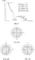
- FIG. 2 is a diagram of the voltage standing wave ratio (VSWR) of the dual band printed antenna 1 in an embodiment of the present invention.
- the X-axis of the diagram stands for the frequency (unit: GHz) and the Y-axis of the diagram stands for the VSWR.
- FIGs. 3A-3C are the radiation patterns of the dual band printed antenna 1 on the X-Y plane, X-Z plane and the Y-Z plane respectively in an embodiment of the present invention.
- the curves illustrated in thick lines are the radiation patterns of the first frequency band (2.4 GHz to 2.5 GHz) and the curves illustrated in dashed lines are the radiation patterns of the second frequency band (5.15 GHz to 5.875 GHz).
- the dual band printed antenna 1 has good VSWR performances in the first frequency band and the second frequency band. As illustrated in FIGs. 3A-3C , each of the radiation patterns of the dual band printed antenna 1 on each of planes is even.
- the dual band printed antenna 1 can produce two resonant frequency bands by using the coupling of the slot 101 having a shape of a single direction and the monopole antenna element 104.
- the design of the slot is simplified, the structural strength and the appearance of the metal substrate 100 can be improved and the required signal transmission quality can be satisfied.
- FIG. 4A is a diagram of a top view of a dual band printed antenna 4 in an embodiment of the present invention.
- FIG. 4B is a diagram of a bottom view of the dual band printed antenna 4 in FIG. 4A in an embodiment of the present invention.
- FIG. 4C is a diagram of cross-sectional view of the dual band printed antenna 4 along a direction A in FIG. 4A in an embodiment of the present invention.
- the dual band printed antenna 4 includes a metal substrate 400, an electrically isolated supporting element 402 and a monopole antenna element 404.
- the metal substrate 400 includes a slot 401 penetrating through two sides of the metal substrate 400.
- the slot 401 stretches along a specific direction, in which the specific direction is X direction.
- the present invention is not limited thereto.
- the slot 401 is an open slot. More specifically, the metal substrate 400 includes an open terminal that is open at an edge of the metal substrate 400 and a close terminal within the metal substrate 400.
- the slot 401 is apart from one edge of the metal substrate 400 by D1, in which D1 is 9 millimeters.
- D1 is 9 millimeters.
- the present invention is not limited thereto.
- the electrically isolated supporting element 402 is formed on the metal substrate 400.
- the structure of the electrically isolated supporting element 402 is identical to the electrically isolated supporting element 102 illustrated in FIGs. 1A-1C . As a result, the detail thereof is not described herein.
- the monopole antenna element 404 is formed on a side of the electrically isolated supporting element 402 opposite to the metal substrate 400 corresponding to the position of the slot 401.
- the monopole antenna element 404 includes a radiation part 405 and a ground part 407.
- the ground part 407 can be grounded through the metal ground element 406.
- the structure and the operation of the radiation part 405 and the ground part 407 are identical to the radiation part 105 and the ground part 107 illustrated in FIGs. 1A-1C . More specifically, the radiation part 405 resonates with the slot 401 to generate a first radiation pattern of a first frequency band and the radiation part 405 resonates itself to generate a second radiation pattern of a second frequency band. As a result, the detail thereof is not described herein.
- the first frequency band has a resonant frequency of 2.4 GHz and the second frequency band has a resonant frequency of 5 GHz. More specifically, in an embodiment, the range of the first frequency band is around 2.4 GHz to 2.5 GHz. The range of the second frequency band is around 5.15 GHz to 5.875 GHz. However, the present invention is not limited thereto.
- the size of the slot 101 may include a length of 20 millimeters and a width of 2 millimeters. However, the present invention is not limited thereto.
- a first terminal P1 and a second terminal P2 of the radiation part 405 are apart from the close terminal and the open terminal of the slot 401 by a length d and a length c.
- the feed point F is apart from the first terminal P1 and the second terminal P2 by a length a and a length b respectively.
- the resonant frequencies of the monopole antenna element 404 in the first frequency band and the second frequency band and the corresponding impedance matching can be adjusted by adjusting the lengths described above.
- the resonant frequency of the first frequency band can be adjusted by adjusting the lengths c and a.
- the impedance matching of the first frequency band can be adjusted by adjusting the length b.
- the resonant frequency of the second frequency band can be adjusted by adjusting the lengths c and a.
- the impedance matching of the second frequency band can be adjusted by adjusting the length b.
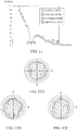
- FIG. 5 is a diagram of the voltage standing wave ratio (VSWR) of the dual band printed antenna 4 in an embodiment of the present invention.
- the X-axis of the diagram stands for the frequency (unit: GHz) and the Y-axis of the diagram stands for the VSWR.
- FIGs. 6A-6C are the radiation patterns of the dual band printed antenna 4 on the X-Y plane, X-Z plane and the Y-Z plane respectively in an embodiment of the present invention.
- the curves illustrated in thick lines are the radiation patterns of the first frequency band (2.4 GHz to 2.5 GHz) and the curves illustrated in dashed lines are the radiation patterns of the second frequency band (5.15 GHz to 5.875 GHz).
- the dual band printed antenna 1 has good VSWR performances in the first frequency band and the second frequency band. As illustrated in FIGs. 6A-6C , each of the radiation patterns of the dual band printed antenna 1 on each plane is even.
- the dual band printed antenna 4 can produce two resonant frequency bands by using the coupling of the slot 401 having a shape of a single direction and the monopole antenna element 404.
- the design of the slot is simplified, the structural strength and the appearance of the metal substrate 400 can be improved and the required signal transmission quality can be satisfied.
- FIG. 7A is a diagram of a top view of a dual band printed antenna 7 in an embodiment of the present invention.
- FIG. 7B is a diagram of a bottom view of the dual band printed antenna 7 in FIG. 7A in an embodiment of the present invention.
- FIG. 7C is a diagram of cross-sectional view of the dual band printed antenna 7 along a direction A in FIG. 7A in an embodiment of the present invention.
- the dual band printed antenna 7 includes a metal substrate 700, an electrically isolated supporting element 702 and an inverted-F antenna element 704.
- the metal substrate 700 includes a slot 701 penetrating through two sides of the metal substrate 700.
- the slot 701 stretches along a specific direction, in which the specific direction is X direction.
- the present invention is not limited thereto.
- the slot 701 is a close slot. More specifically, the two terminals of the slot 701 are within the metal substrate 700.
- the slot 701 is apart from two edges of the metal substrate 700 by D1 and D2, in which D1 and D2 are 9 millimeters and 15 millimeters respectively.
- D1 and D2 are 9 millimeters and 15 millimeters respectively.
- the present invention is not limited thereto.
- the electrically isolated supporting element 702 is formed on the metal substrate 700.
- the structure of the electrically isolated supporting element 702 is identical to the electrically isolated supporting element 102 illustrated in FIGs. 1A-1C . As a result, the detail thereof is not described herein.
- the inverted-F antenna element 704 includes a first radiation part 705A, a second radiation part 705B, a third radiation part 705C and connection radiation parts 705D and 705E.
- the first radiation part 705A stretches along the specific direction and includes a feed point F.
- the second radiation part 705B stretches along the specific direction, is disposed at a first side of the first radiation part 705A, is parallel and adjacent to the first radiation part 705A and is apart from the first radiation part 705A by a first distance.
- the third radiation part 705C stretches along the specific direction, is disposed at a second side of the first radiation part 705A, is parallel and adjacent to the first radiation part 705A and is apart from the first radiation part 705A by a second distance.
- the connection radiation part 705D electrically couples a terminal of the second radiation part 705B to the first radiation part 705A and the connection radiation part 705E electrically couples the other terminal of the second radiation part 705B to the third radiation part 7
- the dual band printed antenna 7 further includes a metal ground element 706 to electrically couple to a part of the second radiation part 705B serving as a ground point to electrically couple the second radiation part 705B to the metal substrate 100 to aid the second radiation part 705B to be grounded.
- the metal ground element 706 can be such as, but not limited to a copper foil.
- the first radiation part 705A, the second radiation part 705B, the third radiation part 705C resonate with the slot 701 to generate a first radiation pattern of a first frequency band and the first radiation part 705A, the second radiation part 705B, the third radiation part 705C resonate themselves to generate a second radiation pattern of a second frequency band.
- the first frequency band has a resonant frequency of 2.4 GHz and the second frequency band has a resonant frequency of 5 GHz. More specifically, in an embodiment, the range of the first frequency band is around 2.4 GHz to 2.5 GHz. The range of the second frequency band is around 5.15 GHz to 5.875 GHz. However, the present invention is not limited thereto.
- the size of the slot 701 may include a length of 45 millimeters and a width of 2 millimeters. However, the present invention is not limited thereto.
- a first terminal P1 and a second terminal P2 of the first radiation part 705A are apart from the two terminals of the slot 701 by a length c and a length e that is smaller than the length c.
- the feed point F is apart from the first terminal P1 and the second terminal P2 by a length d and a length b respectively.
- the third radiation part 705C has a length a. The resonant frequencies of the inverted-F antenna element 704 in the first frequency band and the second frequency band and the corresponding impedance matching can be adjusted by adjusting the lengths described above.
- the resonant frequency of the first frequency band can be adjusted by adjusting the lengths c and a.
- the impedance matching of the first frequency band can be adjusted by adjusting the lengths d and b.
- the resonant frequency of the second frequency band can be adjusted by adjusting the lengths c and d.
- the impedance matching of the second frequency band can be adjusted by adjusting the length b.
- FIG. 8 is a diagram of the voltage standing wave ratio (VSWR) of the dual band printed antenna 7 in an embodiment of the present invention.
- the X-axis of the diagram stands for the frequency (unit: GHz) and the Y-axis of the diagram stands for the VSWR.
- FIGs. 9A-9C are the radiation patterns of the dual band printed antenna 7 on the X-Y plane, X-Z plane and the Y-Z plane respectively in an embodiment of the present invention.
- the curves illustrated in thick lines are the radiation patterns of the first frequency band (2.4 GHz to 2.5 GHz) and the curves illustrated in dashed lines are the radiation patterns of the second frequency band (5.15 GHz to 5.875 GHz).
- the dual band printed antenna 7 has good VSWR performances in the first frequency band and the second frequency band. As illustrated in FIGs. 9A-9C , each of the radiation patterns of the dual band printed antenna 7 on each of planes is even.
- the dual band printed antenna 7 can produce two resonant frequency bands by using the coupling of the slot 701 having a shape of a single direction and the inverted-F antenna element 704.
- the design of the slot is simplified, the structural strength and the appearance of the metal substrate 700 can be improved and the required signal transmission quality can be satisfied.
- FIG. 10A is a diagram of a top view of a dual band printed antenna 10 in an embodiment of the present invention.
- FIG. 10B is a diagram of a bottom view of the dual band printed antenna 10 in FIG. 10A in an embodiment of the present invention.
- FIG. 10C is a diagram of cross-sectional view of the dual band printed antenna 10 along a direction A in FIG. 10A in an embodiment of the present invention.
- the dual band printed antenna 10 includes a metal substrate 1000, an electrically isolated supporting element 1002 and an inverted-F antenna element 1004.
- the metal substrate 1000 includes a slot 1001 penetrating through two sides of the metal substrate 1000.
- the slot 1001 stretches along a specific direction, in which the specific direction is X direction.
- the present invention is not limited thereto.
- the slot 1001 is an open slot. More specifically, the metal substrate 1000 includes an open terminal that is open at an edge of the metal substrate 1000 and a close terminal within the metal substrate 1000.
- the slot 1001 is apart from one edge of the metal substrate 1000 by D1, in which D1 is 9 millimeters.
- D1 is 9 millimeters.
- the present invention is not limited thereto.
- the electrically isolated supporting element 1002 is formed on the metal substrate 1000.
- the structure of the electrically isolated supporting element 1002 is identical to the electrically isolated supporting element 102 illustrated in FIGs. 1A-1C . As a result, the detail thereof is not described herein.
- the inverted-F antenna element 1004 includes a first radiation part 1005A, a second radiation part 1005B, a third radiation part 1005C and connection radiation parts 1005D and 1005E.
- the second radiation part 1005B can also be grounded by using the metal ground element 1006.
- the structure and operation of the first radiation part 1005A, the second radiation part 1005B, the third radiation part 1005C and the connection radiation parts 1005D and 1005E are identical the first radiation part 705A, the second radiation part 705B, the third radiation part 705C and the connection radiation parts 705D and 705E illustrated in FIGs. 7A-7C . More specifically, the first radiation part 1005A, the second radiation part 1005B, the third radiation part 1005C resonate with the slot 1001 to generate a first radiation pattern of a first frequency band and the first radiation part 1005A, the second radiation part 1005B, the third radiation part 1005C resonate themselves to generate a second radiation pattern of a second frequency band. As a result, the detail thereof is not described herein.
- the first frequency band has a resonant frequency of 2.4 GHz and the second frequency band has a resonant frequency of 5 GHz. More specifically, in an embodiment, the range of the first frequency band is around 2.4 GHz to 2.5 GHz. The range of the second frequency band is around 5.15 GHz to 5.875 GHz. However, the present invention is not limited thereto.
- the size of the slot 1001 may include a length of 20 millimeters and a width of 2 millimeters. However, the present invention is not limited thereto.
- a first terminal P1 of the first radiation part 1005A is apart from the open terminal of the slot 1001 by a length c.
- the feed point F is apart from the first terminal P1 and the second terminal by a length d and a length b respectively.
- the third radiation part 1005C has a length a.
- the resonant frequencies of the inverted-F antenna element 1004 in the first frequency band and the second frequency band and the corresponding impedance matching can be adjusted by adjusting the lengths described above.
- the resonant frequency of the first frequency band can be adjusted by adjusting the lengths c and a.
- the impedance matching of the first frequency band can be adjusted by adjusting the lengths b and d.
- the resonant frequency of the second frequency band can be adjusted by adjusting the lengths c and d.
- the impedance matching of the second frequency band can be adjusted by adjusting the length b.
- FIG. 11 is a diagram of the voltage standing wave ratio (VSWR) of the dual band printed antenna 10 in an embodiment of the present invention.
- the X-axis of the diagram stands for the frequency (unit: GHz) and the Y-axis of the diagram stands for the VSWR.
- FIGs. 12A-12C are the radiation patterns of the dual band printed antenna 10 on the X-Y plane, X-Z plane and the Y-Z plane respectively in an embodiment of the present invention.
- the curves illustrated in thick lines are the radiation patterns of the first frequency band (2.4 GHz to 2.5 GHz) and the curves illustrated in dashed lines are the radiation patterns of the second frequency band (5.15 GHz to 5.875 GHz).
- the dual band printed antenna 10 has good VSWR performances in the first frequency band and the second frequency band. As illustrated in FIGs. 12A-12C , each of the radiation patterns of the dual band printed antenna 10 on each of planes is even.
- the dual band printed antenna 10 can produce two resonant frequency bands by using the coupling of the slot 1001 having a shape of a single direction and the inverted-F antenna element 1004.
- the design of the slot is simplified, the structural strength and the appearance of the metal substrate 700 can be improved and the required signal transmission quality can be satisfied.
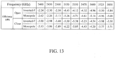
- FIG. 13 is a diagram illustrating average antenna gains under different frequencies when different forms of slots and antenna elements are included in the dual band printed antenna in an embodiment of the present invention.
- the average antenna gains described above is generated when a coaxial transmission line having an impedance of 50 ohms, a core diameter of 1.13 millimeters and a length of 500 millimeters is used.
- the antenna efficiency corresponding to the resonant frequency 2.4 of GHz is -2.9 dB to -5.1 dB.
- the antenna efficiency corresponding to the resonant frequency 5 of GHz is -3.7 dB to -6.2 dB.
- the antenna efficiency corresponding to the resonant frequency 2.4 of GHz is -2.1 dB to -2.6 dB.
- the antenna efficiency corresponding to the resonant frequency 5 of GHz is -4.6 dB to -5.2 dB.
- the antenna efficiency corresponding to the resonant frequency 2.4 of GHz is -2.9 dB to -3.4 dB.
- the antenna efficiency corresponding to the resonant frequency 5 of GHz is -3.5 dB to -5.5 dB.
- the antenna efficiency corresponding to the resonant frequency 2.4 of GHz is -2.2 dB to -2.5 dB.
- the antenna efficiency corresponding to the resonant frequency 5 of GHz is -4.1 dB to -5.8 dB.
- the dual band printed antenna has a great performance in the antenna efficiency.
Landscapes
- Engineering & Computer Science (AREA)
- Computer Networks & Wireless Communication (AREA)
- Details Of Aerials (AREA)
- Waveguide Aerials (AREA)
- Variable-Direction Aerials And Aerial Arrays (AREA)
Description
- The present invention relates to an antenna technology. More particularly, the present invention relates to a dual band printed antenna.
- Along with the rapid development of the network technology, the electronic communication devices that are able to connect to network become indispensable in our daily life. Simultaneously, the requirements of the design of appearance and the convenience of the portability of the electronic communication devices become higher due to the popularity thereof. Document
EP 3113285 A1 provides a mobile device with a novel antenna structure. DocumentEP 1831955 A1 provides an antenna structure for a wireless device comprising a ground plane and an antenna element. DocumentUS 20150311594 A1 provides an electronic device with hybrid planar inverted-F slot antennas and indirectly fed slot antennas. DocumentEP 1401050 A1 provides an internal planar antenna for small radio apparatuses. In general, in order to shrink the volume of the electronic communication devices, most manufacturers make improvement on the printed antenna. However, not only the adjustment and control of operation frequencies need to be taken into consideration when the electronic communication devices are modified to make improvement, but also the human resource cost spent during the manufacturing process is needed to be evaluated. - Accordingly, it is a great challenge to design shrunk printed antennas under the condition that the normal operation is not affected and manufacturing cost is lowered.
- The object of the present application is solved by the independent claims. Advantageous embodiments are described by the dependent claims. The invention provides a dual band printed antenna that includes a metal substrate, an electrically isolated supporting element and a monopole antenna element. The metal substrate includes a slot. A side of the electrically isolated supporting element is formed on the metal substrate. The monopole antenna element is formed on the other side of the electrically isolated supporting element and corresponding to the position of the slot, and the monopole antenna element includes a radiation part and a ground part. The radiation part includes a feed point. The ground part is separated from the radiation part for a distance. The radiation part resonates with the slot to generate a first radiation pattern of a first frequency band and the radiation part resonates itself to generate a second radiation pattern of a second frequency band.
- Another aspect of the present invention is to provide a dual band printed antenna that includes a metal substrate, an electrically isolated supporting element and an inverted-F antenna element. The metal substrate includes a slot. A side of the electrically isolated supporting element is formed on the metal substrate. The inverted-F antenna element is formed on the other side of the electrically isolated supporting element and corresponding to the position of the slot, and the inverted-F antenna element includes at least one radiation part comprising a feed point and a ground point. The radiation part resonates with the slot to generate a first radiation pattern of a first frequency band and the radiation part resonates itself to generate a second radiation pattern of a second frequency band.
- These and other features, aspects, and advantages of the present invention will become better understood with reference to the following description and appended claims.
- It is to be understood that both the foregoing general description and the following detailed description are by examples, and are intended to provide further explanation of the invention as claimed.
- The invention can be more fully understood by reading the following detailed description of the embodiment, with reference made to the accompanying drawings as follows:
-
FIG. 1A is a diagram of a top view of a dual band printed antenna in an embodiment of the present invention; -
FIG. 1B is a diagram of a bottom view of the dual band printed antenna inFIG. 1A in an embodiment of the present invention; -
FIG. 1C is a diagram of cross-sectional view of the dual band printed antenna along a direction A inFIG. 1A in an embodiment of the present invention; -
FIG. 2 is a diagram of the voltage standing wave ratio of the dual band printed antenna in an embodiment of the present invention; -
FIGs. 3A-3C are the radiation patterns of the dual band printed antenna on the X-Y plane, X-Z plane and the Y-Z plane respectively in an embodiment of the present invention; -
FIG. 4A is a diagram of a top view of a dual band printed antenna in an embodiment of the present invention; -
FIG. 4B is a diagram of a bottom view of the dual band printed antenna inFIG. 4A in an embodiment of the present invention; -
FIG. 4C is a diagram of cross-sectional view of the dual band printed antenna along a direction A inFIG. 4A in an embodiment of the present invention; -
FIG. 5 is a diagram of the voltage standing wave ratio of the dual band printed antenna in an embodiment of the present invention; -
FIGs. 6A-6C are the radiation patterns of the dual band printed antenna on the X-Y plane, X-Z plane and the Y-Z plane respectively in an embodiment of the present invention; -
FIG. 7A is a diagram of a top view of a dual band printed antenna in an embodiment of the present invention; -
FIG. 7B is a diagram of a bottom view of the dual band printed antenna inFIG. 1A in an embodiment of the present invention; -
FIG. 7C is a diagram of cross-sectional view of the dual band printed antenna along a direction A inFIG. 7A in an embodiment of the present invention; -
FIG. 8 is a diagram of the voltage standing wave ratio of the dual band printed antenna in an embodiment of the present invention; -
FIGs. 9A-9C are the radiation patterns of the dual band printed antenna on the X-Y plane, X-Z plane and the Y-Z plane respectively in an embodiment of the present invention; -
FIG. 10A is a diagram of a top view of a dual band printed antenna in an embodiment of the present invention; -
FIG. 10B is a diagram of a bottom view of the dual band printed antenna inFIG. 10A in an embodiment of the present invention; -
FIG. 10C is a diagram of cross-sectional view of the dual band printed antenna along a direction A inFIG. 10A in an embodiment of the present invention; -
FIG. 11 is a diagram of the voltage standing wave ratio of the dual band printed antenna in an embodiment of the present invention; -
FIGs. 12A-12C are the radiation patterns of the dual band printed antenna on the X-Y plane, X-Z plane and the Y-Z plane respectively in an embodiment of the present invention; and -
FIG. 13 is a diagram illustrating average antenna gains under different frequencies when different forms of slots and antenna elements are included in the dual band printed antenna in an embodiment of the present invention. - Reference will now be made in detail to the present embodiments of the invention, examples of which are illustrated in the accompanying drawings. Wherever possible, the same reference numbers are used in the drawings and the description to refer to the same or like parts.
- As used herein with respect to the "first", "second", ..., etc., are not particularly alleged order or overall meaning, nor to limit the present invention, it is only the difference between the same technique described in terms elements or operations.
- As used herein with respect to "electrically connected" or "coupled" may refer to two or more elements are in direct physical or electrical contact as, or as a solid or indirect mutual electrical contact, and the "power connection "can also refer to two or more elements are in operation or action.
- As used herein with respect to the "including", "includes", "having", "containing", etc., are open terms that mean including but not limited to.
- The term "and / or" includes the things on any or all combinations used herein.
- As used herein with respect to the direction of the term, for example: up, down, left, right, front or rear, etc., only the direction reference to the drawings. Therefore, the direction of the use of terminology is used to describe not intended to limit this creation.
- Certain terms used to describe the present application will be discussed below or elsewhere in this specification, in order to provide those skilled in the additional guidance on the description of the present application.
- ] As used herein, the term on the "approximately", "about" etc., to any number of modifications or errors can change slightly, but a slight change or error does not change its nature. In general, such terms of changes or errors in some embodiments, be 20%, in some embodiments, may be 10%, and in some embodiments may be 5% or some other value. Those skilled in the art should understand that the above-mentioned value as per needs adjustment, not limited thereto.
- Reference is now made to
FIG. 1A, FIG. 1B and FIG. 1C. FIG. 1A is a diagram of a top view of a dual band printedantenna 1 in an embodiment of the present invention.FIG. 1B is a diagram of a bottom view of the dual band printedantenna 1 inFIG. 1A in an embodiment of the present invention.FIG. 1C is a diagram of cross-sectional view of the dual band printedantenna 1 along a direction A inFIG. 1A in an embodiment of the present invention. The dual band printedantenna 1 includes ametal substrate 100, an electrically isolated supportingelement 102 and amonopole antenna element 104. - The
metal substrate 100 includes aslot 101 penetrating through two sides of themetal substrate 100. In the present embodiment, theslot 101 stretches along a specific direction, in which the specific direction is X direction. However, the present invention is not limited thereto. In the present embodiment, theslot 101 is a close slot. More specifically, the two terminals of theslot 101 are within themetal substrate 100. - In an embodiment, in order to maintain the structural strength of the
metal substrate 100, theslot 101 is apart from two edges of themetal substrate 100 by D1 and D2, in which D1 and D2 are 9 millimeters and 15 millimeters respectively. However, the present invention is not limited thereto. - The electrically isolated supporting
element 102 is formed on themetal substrate 100. In an embodiment, the electrically isolated supportingelement 102 covers theslot 101. In other embodiment, the electrically isolated supportingelement 102 may partially cover theslot 101. - In an embodiment, the electrically isolated supporting
element 102 includes an electrically isolated supportinglayer 103A and acircuit board layer 103B adjacent to each other. A side of the electrically isolated supportinglayer 103A is disposed on themetal substrate 100 and thecircuit board 103B is disposed at another side of the electrically isolated supportinglayer 103A opposite to themetal substrate 100 such that themonopole antenna element 104 is disposed at a side of thecircuit board layer 103B opposite to the electrically isolated supportinglayer 103A. In an embodiment, in order to accomplish a better electrically isolating effect between themonopole antenna element 104 and themetal substrate 100 underneath and a better coupling effect between themonopole antenna element 104 and theslot 101, the thicknesses of the electrically isolated supportinglayer 103A and thecircuit board 103B can be 1 millimeter and 0.4 millimeters respectively. However, the present invention is not limited thereto. - The
monopole antenna element 104 is formed on the electrically isolated supportinglayer 103A corresponding to the position of theslot 101. Themonopole antenna element 104 includes aradiation part 105 and aground part 107. - The
radiation part 105 includes a feed point F. Theground part 107 is separated from theradiation part 105 for a distance. In an embodiment, both theradiation part 105 and theground part 107 stretch along the specific direction. However, the present invention is not limited thereto. In an embodiment, the dual band printedantenna 1 further includes ametal ground element 106 to be electrically coupled to theground part 107 and themetal substrate 100 to aid theground part 107 to be grounded. Themetal ground element 106 can be such as, but not limited to a copper foil. - For example, the
monopole antenna element 104 of the dual band printedantenna 1 can be driven to be in operation by disposing a transmission line (not illustrated) that includes a positive terminal electrically coupled to the feed point F and a negative terminal electrically coupled to themetal ground element 106 further to the ground. - When the
monopole antenna element 104 is in operation, theradiation part 105 resonates with theslot 101 to generate a first radiation pattern of a first frequency band and theradiation part 105 resonates itself to generate a second radiation pattern of a second frequency band. - In an embodiment, the first frequency band has a resonant frequency of 2.4 GHz and the second frequency band has a resonant frequency of 5 GHz. More specifically, in an embodiment, the range of the first frequency band is around 2.4 GHz to 2.5 GHz. The range of the second frequency band is around 5.15 GHz to 5.875 GHz. However, the present invention is not limited thereto. When the first frequency band is around 2.4 GHz, in order to accomplish a better resonating effect between the
radiation part 105 and theslot 101, the size of theslot 101 may include a length of 45 millimeters and a width of 2 millimeters. However, the present invention is not limited thereto. - In the present embodiment, a first terminal P1 and a second terminal P2 of the
radiation part 105 are apart from the two terminals of theslot 101 by a length c and a length d that is larger than the length c. The feed point F is apart from the first terminal P1 and the second terminal P2 by a length a and a length b respectively. The resonant frequencies of themonopole antenna element 104 in the first frequency band and the second frequency band and the corresponding impedance matching can be adjusted by adjusting the lengths described above. - More specifically, the resonant frequency of the first frequency band can be adjusted by adjusting the lengths c and b. The impedance matching of the first frequency band can be adjusted by adjusting the length a. The resonant frequency of the second frequency band can be adjusted by adjusting the lengths c and b. The impedance matching of the second frequency band can be adjusted by adjusting the length b.
- Reference is now made to
FIG. 2 and FIGs. 3A-3C. FIG. 2 is a diagram of the voltage standing wave ratio (VSWR) of the dual band printedantenna 1 in an embodiment of the present invention. The X-axis of the diagram stands for the frequency (unit: GHz) and the Y-axis of the diagram stands for the VSWR. -
FIGs. 3A-3C are the radiation patterns of the dual band printedantenna 1 on the X-Y plane, X-Z plane and the Y-Z plane respectively in an embodiment of the present invention. The curves illustrated in thick lines are the radiation patterns of the first frequency band (2.4 GHz to 2.5 GHz) and the curves illustrated in dashed lines are the radiation patterns of the second frequency band (5.15 GHz to 5.875 GHz). - As illustrated in
FIG. 2 , the dual band printedantenna 1 has good VSWR performances in the first frequency band and the second frequency band. As illustrated inFIGs. 3A-3C , each of the radiation patterns of the dual band printedantenna 1 on each of planes is even. - As a result, the dual band printed
antenna 1 can produce two resonant frequency bands by using the coupling of theslot 101 having a shape of a single direction and themonopole antenna element 104. The design of the slot is simplified, the structural strength and the appearance of themetal substrate 100 can be improved and the required signal transmission quality can be satisfied. - Reference is now made to
FIG. 4A, FIG. 4B and FIG. 4C. FIG. 4A is a diagram of a top view of a dual band printedantenna 4 in an embodiment of the present invention.FIG. 4B is a diagram of a bottom view of the dual band printedantenna 4 inFIG. 4A in an embodiment of the present invention.FIG. 4C is a diagram of cross-sectional view of the dual band printedantenna 4 along a direction A inFIG. 4A in an embodiment of the present invention. The dual band printedantenna 4 includes ametal substrate 400, an electrically isolated supportingelement 402 and amonopole antenna element 404. - The
metal substrate 400 includes aslot 401 penetrating through two sides of themetal substrate 400. In the present embodiment, theslot 401 stretches along a specific direction, in which the specific direction is X direction. However, the present invention is not limited thereto. In the present embodiment, theslot 401 is an open slot. More specifically, themetal substrate 400 includes an open terminal that is open at an edge of themetal substrate 400 and a close terminal within themetal substrate 400. - In an embodiment, in order to maintain the structural strength of the
metal substrate 400, theslot 401 is apart from one edge of themetal substrate 400 by D1, in which D1 is 9 millimeters. However, the present invention is not limited thereto. - The electrically isolated supporting
element 402 is formed on themetal substrate 400. The structure of the electrically isolated supportingelement 402 is identical to the electrically isolated supportingelement 102 illustrated inFIGs. 1A-1C . As a result, the detail thereof is not described herein. - The
monopole antenna element 404 is formed on a side of the electrically isolated supportingelement 402 opposite to themetal substrate 400 corresponding to the position of theslot 401. Themonopole antenna element 404 includes aradiation part 405 and aground part 407. Theground part 407 can be grounded through themetal ground element 406. The structure and the operation of theradiation part 405 and theground part 407 are identical to theradiation part 105 and theground part 107 illustrated inFIGs. 1A-1C . More specifically, theradiation part 405 resonates with theslot 401 to generate a first radiation pattern of a first frequency band and theradiation part 405 resonates itself to generate a second radiation pattern of a second frequency band. As a result, the detail thereof is not described herein. - In an embodiment, the first frequency band has a resonant frequency of 2.4 GHz and the second frequency band has a resonant frequency of 5 GHz. More specifically, in an embodiment, the range of the first frequency band is around 2.4 GHz to 2.5 GHz. The range of the second frequency band is around 5.15 GHz to 5.875 GHz. However, the present invention is not limited thereto. When the first frequency band is around 2.4 GHz, in order to accomplish a better resonating effect between the
radiation part 105 and theslot 101, the size of theslot 101 may include a length of 20 millimeters and a width of 2 millimeters. However, the present invention is not limited thereto. - In the present embodiment, a first terminal P1 and a second terminal P2 of the
radiation part 405 are apart from the close terminal and the open terminal of theslot 401 by a length d and a length c. The feed point F is apart from the first terminal P1 and the second terminal P2 by a length a and a length b respectively. The resonant frequencies of themonopole antenna element 404 in the first frequency band and the second frequency band and the corresponding impedance matching can be adjusted by adjusting the lengths described above. - More specifically, the resonant frequency of the first frequency band can be adjusted by adjusting the lengths c and a. The impedance matching of the first frequency band can be adjusted by adjusting the length b. The resonant frequency of the second frequency band can be adjusted by adjusting the lengths c and a. The impedance matching of the second frequency band can be adjusted by adjusting the length b.
- Reference is now made to
FIG. 5 and FIGs. 6A-6C. FIG. 5 is a diagram of the voltage standing wave ratio (VSWR) of the dual band printedantenna 4 in an embodiment of the present invention. The X-axis of the diagram stands for the frequency (unit: GHz) and the Y-axis of the diagram stands for the VSWR. -
FIGs. 6A-6C are the radiation patterns of the dual band printedantenna 4 on the X-Y plane, X-Z plane and the Y-Z plane respectively in an embodiment of the present invention. The curves illustrated in thick lines are the radiation patterns of the first frequency band (2.4 GHz to 2.5 GHz) and the curves illustrated in dashed lines are the radiation patterns of the second frequency band (5.15 GHz to 5.875 GHz). - As illustrated in
FIG. 5 , the dual band printedantenna 1 has good VSWR performances in the first frequency band and the second frequency band. As illustrated inFIGs. 6A-6C , each of the radiation patterns of the dual band printedantenna 1 on each plane is even. - As a result, the dual band printed
antenna 4 can produce two resonant frequency bands by using the coupling of theslot 401 having a shape of a single direction and themonopole antenna element 404. The design of the slot is simplified, the structural strength and the appearance of themetal substrate 400 can be improved and the required signal transmission quality can be satisfied. - Reference is now made to
FIG. 7A ,FIG. 7B and FIG. 7C .FIG. 7A is a diagram of a top view of a dual band printedantenna 7 in an embodiment of the present invention.FIG. 7B is a diagram of a bottom view of the dual band printedantenna 7 inFIG. 7A in an embodiment of the present invention.FIG. 7C is a diagram of cross-sectional view of the dual band printedantenna 7 along a direction A inFIG. 7A in an embodiment of the present invention. The dual band printedantenna 7 includes ametal substrate 700, an electrically isolated supportingelement 702 and an inverted-F antenna element 704. - The
metal substrate 700 includes aslot 701 penetrating through two sides of themetal substrate 700. In the present embodiment, theslot 701 stretches along a specific direction, in which the specific direction is X direction. However, the present invention is not limited thereto. In the present embodiment, theslot 701 is a close slot. More specifically, the two terminals of theslot 701 are within themetal substrate 700. - In an embodiment, in order to maintain the structural strength of the
metal substrate 700, theslot 701 is apart from two edges of themetal substrate 700 by D1 and D2, in which D1 and D2 are 9 millimeters and 15 millimeters respectively. However, the present invention is not limited thereto. - The electrically isolated supporting
element 702 is formed on themetal substrate 700. The structure of the electrically isolated supportingelement 702 is identical to the electrically isolated supportingelement 102 illustrated inFIGs. 1A-1C . As a result, the detail thereof is not described herein. - The inverted-
F antenna element 704 includes afirst radiation part 705A, asecond radiation part 705B, athird radiation part 705C andconnection radiation parts 705D and 705E. Thefirst radiation part 705A stretches along the specific direction and includes a feed point F. Thesecond radiation part 705B stretches along the specific direction, is disposed at a first side of thefirst radiation part 705A, is parallel and adjacent to thefirst radiation part 705A and is apart from thefirst radiation part 705A by a first distance. Thethird radiation part 705C stretches along the specific direction, is disposed at a second side of thefirst radiation part 705A, is parallel and adjacent to thefirst radiation part 705A and is apart from thefirst radiation part 705A by a second distance. The connection radiation part 705D electrically couples a terminal of thesecond radiation part 705B to thefirst radiation part 705A and theconnection radiation part 705E electrically couples the other terminal of thesecond radiation part 705B to thethird radiation part 705C. - In an embodiment, the dual band printed
antenna 7 further includes ametal ground element 706 to electrically couple to a part of thesecond radiation part 705B serving as a ground point to electrically couple thesecond radiation part 705B to themetal substrate 100 to aid thesecond radiation part 705B to be grounded. Themetal ground element 706 can be such as, but not limited to a copper foil. - When the inverted-
F antenna element 704 is in operation, thefirst radiation part 705A, thesecond radiation part 705B, thethird radiation part 705C resonate with theslot 701 to generate a first radiation pattern of a first frequency band and thefirst radiation part 705A, thesecond radiation part 705B, thethird radiation part 705C resonate themselves to generate a second radiation pattern of a second frequency band. - In an embodiment, the first frequency band has a resonant frequency of 2.4 GHz and the second frequency band has a resonant frequency of 5 GHz. More specifically, in an embodiment, the range of the first frequency band is around 2.4 GHz to 2.5 GHz. The range of the second frequency band is around 5.15 GHz to 5.875 GHz. However, the present invention is not limited thereto. When the first frequency band is around 2.4 GHz, in order to accomplish a better resonating effect between the
first radiation part 705A, thesecond radiation part 705B, thethird radiation part 705C and theslot 701, the size of theslot 701 may include a length of 45 millimeters and a width of 2 millimeters. However, the present invention is not limited thereto. - In the present embodiment, a first terminal P1 and a second terminal P2 of the
first radiation part 705A are apart from the two terminals of theslot 701 by a length c and a length e that is smaller than the length c. The feed point F is apart from the first terminal P1 and the second terminal P2 by a length d and a length b respectively. Thethird radiation part 705C has a length a. The resonant frequencies of the inverted-F antenna element 704 in the first frequency band and the second frequency band and the corresponding impedance matching can be adjusted by adjusting the lengths described above. - More specifically, the resonant frequency of the first frequency band can be adjusted by adjusting the lengths c and a. The impedance matching of the first frequency band can be adjusted by adjusting the lengths d and b. The resonant frequency of the second frequency band can be adjusted by adjusting the lengths c and d. The impedance matching of the second frequency band can be adjusted by adjusting the length b.
- Reference is now made to
FIG. 8 and FIGs. 9A-9C. FIG. 8 is a diagram of the voltage standing wave ratio (VSWR) of the dual band printedantenna 7 in an embodiment of the present invention. The X-axis of the diagram stands for the frequency (unit: GHz) and the Y-axis of the diagram stands for the VSWR. -
FIGs. 9A-9C are the radiation patterns of the dual band printedantenna 7 on the X-Y plane, X-Z plane and the Y-Z plane respectively in an embodiment of the present invention. The curves illustrated in thick lines are the radiation patterns of the first frequency band (2.4 GHz to 2.5 GHz) and the curves illustrated in dashed lines are the radiation patterns of the second frequency band (5.15 GHz to 5.875 GHz). - As illustrated in
FIG. 8 , the dual band printedantenna 7 has good VSWR performances in the first frequency band and the second frequency band. As illustrated inFIGs. 9A-9C , each of the radiation patterns of the dual band printedantenna 7 on each of planes is even. - As a result, the dual band printed
antenna 7 can produce two resonant frequency bands by using the coupling of theslot 701 having a shape of a single direction and the inverted-F antenna element 704. The design of the slot is simplified, the structural strength and the appearance of themetal substrate 700 can be improved and the required signal transmission quality can be satisfied. - Reference is now made to
FIG. 10A ,FIG. 10B and FIG. 10C .FIG. 10A is a diagram of a top view of a dual band printedantenna 10 in an embodiment of the present invention.FIG. 10B is a diagram of a bottom view of the dual band printedantenna 10 inFIG. 10A in an embodiment of the present invention.FIG. 10C is a diagram of cross-sectional view of the dual band printedantenna 10 along a direction A inFIG. 10A in an embodiment of the present invention. The dual band printedantenna 10 includes ametal substrate 1000, an electrically isolated supportingelement 1002 and an inverted-F antenna element 1004. - The
metal substrate 1000 includes aslot 1001 penetrating through two sides of themetal substrate 1000. In the present embodiment, theslot 1001 stretches along a specific direction, in which the specific direction is X direction. However, the present invention is not limited thereto. In the present embodiment, theslot 1001 is an open slot. More specifically, themetal substrate 1000 includes an open terminal that is open at an edge of themetal substrate 1000 and a close terminal within themetal substrate 1000. - In an embodiment, in order to maintain the structural strength of the
metal substrate 1000, theslot 1001 is apart from one edge of themetal substrate 1000 by D1, in which D1 is 9 millimeters. However, the present invention is not limited thereto. - The electrically isolated supporting
element 1002 is formed on themetal substrate 1000. The structure of the electrically isolated supportingelement 1002 is identical to the electrically isolated supportingelement 102 illustrated inFIGs. 1A-1C . As a result, the detail thereof is not described herein. - The inverted-
F antenna element 1004 includes afirst radiation part 1005A, asecond radiation part 1005B, athird radiation part 1005C andconnection radiation parts second radiation part 1005B can also be grounded by using themetal ground element 1006. - The structure and operation of the
first radiation part 1005A, thesecond radiation part 1005B, thethird radiation part 1005C and theconnection radiation parts first radiation part 705A, thesecond radiation part 705B, thethird radiation part 705C and theconnection radiation parts 705D and 705E illustrated inFIGs. 7A-7C . More specifically, thefirst radiation part 1005A, thesecond radiation part 1005B, thethird radiation part 1005C resonate with theslot 1001 to generate a first radiation pattern of a first frequency band and thefirst radiation part 1005A, thesecond radiation part 1005B, thethird radiation part 1005C resonate themselves to generate a second radiation pattern of a second frequency band. As a result, the detail thereof is not described herein. - In an embodiment, the first frequency band has a resonant frequency of 2.4 GHz and the second frequency band has a resonant frequency of 5 GHz. More specifically, in an embodiment, the range of the first frequency band is around 2.4 GHz to 2.5 GHz. The range of the second frequency band is around 5.15 GHz to 5.875 GHz. However, the present invention is not limited thereto. When the first frequency band is around 2.4 GHz, in order to accomplish a better resonating effect between the
first radiation part 1005A, thesecond radiation part 1005B, thethird radiation part 1005C and theslot 1001, the size of theslot 1001 may include a length of 20 millimeters and a width of 2 millimeters. However, the present invention is not limited thereto. - In the present embodiment, a first terminal P1 of the
first radiation part 1005A is apart from the open terminal of theslot 1001 by a length c. The feed point F is apart from the first terminal P1 and the second terminal by a length d and a length b respectively. Thethird radiation part 1005C has a length a. The resonant frequencies of the inverted-F antenna element 1004 in the first frequency band and the second frequency band and the corresponding impedance matching can be adjusted by adjusting the lengths described above. - More specifically, the resonant frequency of the first frequency band can be adjusted by adjusting the lengths c and a. The impedance matching of the first frequency band can be adjusted by adjusting the lengths b and d. The resonant frequency of the second frequency band can be adjusted by adjusting the lengths c and d. The impedance matching of the second frequency band can be adjusted by adjusting the length b.
- Reference is now made to
FIG. 11 and FIGs. 12A-12C. FIG. 11 is a diagram of the voltage standing wave ratio (VSWR) of the dual band printedantenna 10 in an embodiment of the present invention. The X-axis of the diagram stands for the frequency (unit: GHz) and the Y-axis of the diagram stands for the VSWR. -
FIGs. 12A-12C are the radiation patterns of the dual band printedantenna 10 on the X-Y plane, X-Z plane and the Y-Z plane respectively in an embodiment of the present invention. The curves illustrated in thick lines are the radiation patterns of the first frequency band (2.4 GHz to 2.5 GHz) and the curves illustrated in dashed lines are the radiation patterns of the second frequency band (5.15 GHz to 5.875 GHz). - As illustrated in
FIG. 11 , the dual band printedantenna 10 has good VSWR performances in the first frequency band and the second frequency band. As illustrated inFIGs. 12A-12C , each of the radiation patterns of the dual band printedantenna 10 on each of planes is even. - As a result, the dual band printed
antenna 10 can produce two resonant frequency bands by using the coupling of theslot 1001 having a shape of a single direction and the inverted-F antenna element 1004. The design of the slot is simplified, the structural strength and the appearance of themetal substrate 700 can be improved and the required signal transmission quality can be satisfied. - Reference is now made to
FIG. 13. FIG. 13 is a diagram illustrating average antenna gains under different frequencies when different forms of slots and antenna elements are included in the dual band printed antenna in an embodiment of the present invention. In an embodiment, the average antenna gains described above is generated when a coaxial transmission line having an impedance of 50 ohms, a core diameter of 1.13 millimeters and a length of 500 millimeters is used. - When the dual band printed antenna has a open slot and an inverted-F antenna element, the antenna efficiency corresponding to the resonant frequency 2.4 of GHz is -2.9 dB to -5.1 dB. The antenna efficiency corresponding to the
resonant frequency 5 of GHz is -3.7 dB to -6.2 dB. - When the dual band printed antenna has a open slot and monopole antenna element, the antenna efficiency corresponding to the resonant frequency 2.4 of GHz is -2.1 dB to -2.6 dB. The antenna efficiency corresponding to the
resonant frequency 5 of GHz is -4.6 dB to -5.2 dB. - When the dual band printed antenna has a close slot and inverted-F antenna element, the antenna efficiency corresponding to the resonant frequency 2.4 of GHz is -2.9 dB to -3.4 dB. The antenna efficiency corresponding to the
resonant frequency 5 of GHz is -3.5 dB to -5.5 dB. - When the dual band printed antenna has a close slot and monopole antenna element, the antenna efficiency corresponding to the resonant frequency 2.4 of GHz is -2.2 dB to -2.5 dB. The antenna efficiency corresponding to the
resonant frequency 5 of GHz is -4.1 dB to -5.8 dB. - As a result, whether being in operation at the resonant frequencies of 2.4 GHz or 5 GHz, the dual band printed antenna has a great performance in the antenna efficiency.
Claims (20)
- A dual band printed antenna (1) comprising a metal substrate (100) and an electrically isolated supporting element (102), wherein the metal substrate comprises a slot (101), wherein a side of the electrically isolated supporting element is formed on the metal substrate, characterized in that the dual band printed antenna comprises:
a monopole antenna element (104) formed on the other side of the electrically isolated supporting element and corresponding to the position of the slot, and the monopole antenna element comprises:a radiation part (105) comprising a feed point (F); anda ground part (107) separated from the radiation part for a distance;wherein the electrically isolated supporting element is plate-shaped, wherein the side and the other side of the electrically isolated supporting element are the opposite sides of the electrically isolated supporting element, wherein the radiation part is configured to resonate with the slot configured to generate a first radiation pattern of a first frequency band and the radiation part is configured to resonate itself to generate a second radiation pattern of a second frequency band;wherein the slot stretches along a specific direction (X), wherein two ends of the slot are within the metal substrate;wherein the radiation part and the ground part are cuboid-shaped, wherein the radiation part and the ground part stretch along the specific direction, a first end (P1) and a second end (P2) of the radiation part are respectively apart from the two ends of the slot by a first length (c) and a second length (d) that is larger than the first length, and the feed point is apart from the first end and the second end by a third length (a) and a fourth length (b) respectively;wherein a first resonant frequency of the first frequency band is adjustable by the first length and the fourth length, and a first impedance matching of the monopole antenna element corresponding to the first frequency band is adjustable by the third length;wherein a second resonant frequency of the second frequency band is adjustable by the first length and the fourth length, and a second impedance matching of the monopole antenna element corresponding to the second frequency band is adjustable by the fourth length. - The dual band printed antenna of claim 1, characterized in that the slot is a rectangular slot.
- The dual band printed antenna of claim 1, characterized in that the length of the slot is 45 millimeters and the width of the slot is 2 millimeters.
- The dual band printed antenna of claim 1, characterized in that the electrically isolated supporting element comprises an electrically isolated supporting layer (103A) and a circuit board layer (103B) adjacent to each other, the electrically isolated supporting layer is disposed on the metal substrate, the circuit board layer is disposed at a side of the electrically isolated supporting layer opposite to the metal substrate and the monopole antenna element is disposed at a side of the circuit board layer opposite to the electrically isolated supporting layer.
- The dual band printed antenna of claim 4, characterized in that the thickness of the electrically isolated supporting layer is 1 millimeter and the thickness of the circuit board is 0.4 millimeters.
- The dual band printed antenna of claim 1, characterized in that the dual band printed antenna further comprising a metal ground element (106) to be electrically coupled to the ground part and the metal substrate to aid the ground part to be grounded.
- A dual band printed antenna (7) comprising a metal substrate (700) and an electrically isolated supporting element (702), wherein the metal substrate comprises a slot (701), wherein the electrically isolated supporting element is formed on a side of the metal substrate, characterized in that the dual band printed antenna comprises:an inverted-F antenna element (704) formed on the other side of the electrically isolated supporting element and corresponding to the position of the slot, and the inverted-F antenna element comprises at least one radiation part (705A, 705B, 705C, 705D, 705E) comprising a feed point (F) and a ground point;wherein the electrically isolated supporting element is plate-shaped, wherein the radiation part is configured to resonate with the slot configured to generate a first radiation pattern of a first frequency band and the radiation part is configured to resonate itself to generate a second radiation pattern of a second frequency band;wherein the slot stretches along a specific direction (X), wherein two ends of the slot are within the metal substrate;wherein the inverted-F antenna further comprises a first radiation part (705A) stretching along the specific direction and comprising the feed point, wherein the first radiation part is cuboid-shaped;wherein the inverted-F antenna further comprises a third radiation part (705C) stretching along the specific direction, wherein the third radiation part is cuboid-shaped and disposed at a second side of the first radiation part, being parallel and adjacent to the first radiation part and apart from the first radiation part by a second distance;wherein a first end (P1) and a second end (P2) of the first radiation part are respectively apart from the two ends of the slot by a first length (c) and a second length (e) that is smaller than the first length, the feed point is apart from the first end and the second end by a third length (d) and a fourth length (b) respectively and the third radiation part has a fifth length (a);wherein a first resonant frequency of the first frequency band is adjustable by the first length and the fifth length, and a first impedance matching of the inverted-F antenna element corresponding to the first frequency band is adjustable by the third length and the fourth length;wherein a second resonant frequency of the second frequency band adjustable by the first length and the third length, and a second impedance matching of the inverted-F antenna element corresponding to the second frequency band is adjustable by the fourth length.
- The dual band printed antenna of claim 7, characterized in that the slot is a rectangular slot.
- The dual band printed antenna of claim 7, characterized in that the inverted-F antenna further comprises:a second radiation part (705B) stretching along the specific direction, wherein the second radiation part is cuboid-shaped and disposed at a first side of the first radiation part, being parallel and adjacent to the first radiation part, apart from the first radiation part by a first distance and comprising the ground point; andtwo connection radiation parts (705D, 705E) electrically coupling an end of the second radiation part to the first radiation part and electrically coupling the other end of the second radiation part to the third radiation part.
- The dual band printed antenna of claim 7, characterized in that the electrically isolated supporting element comprises an electrically isolated supporting layer and a circuit board layer adjacent to each other, the electrically isolated supporting layer is disposed at a side of the metal substrate, the circuit board is disposed at an opposite side of the metal substrate and the inverted-F antenna element is disposed at one side of the circuit board opposite to the electrically isolated supporting layer.
- The dual band printed antenna of claim 7, characterized in that the dual band printed antenna further comprising a metal ground element (706) to be electrically coupled to the ground part and the metal substrate to aid the ground part to be grounded.
- A dual band printed antenna (4) comprising a metal substrate (400) and an electrically isolated supporting element (402), wherein the metal substrate comprises a slot (401), wherein a side of the electrically isolated supporting element is formed on the metal substrate, characterized in that the dual band printed antenna comprises:
a monopole antenna element (404) formed on the other side of the electrically isolated supporting element and corresponding to the position of the slot, and the monopole antenna element comprises:a radiation part (405) comprising a feed point (F); anda ground part (407) separated from the radiation part for a distance;wherein the electrically isolated supporting element is plate-shaped, wherein the side and the other side of the electrically isolated supporting element are the opposite sides of the electrically isolated supporting element, wherein the radiation part is configured to resonate with the slot configured to generate a first radiation pattern of a first frequency band and the radiation part is configured to resonate itself to generate a second radiation pattern of a second frequency band;wherein the slot stretches along a specific direction (X), wherein the slot comprises a close end and an open end, and the open end is open at an edge of the metal substrate;wherein the radiation part and the ground part are cuboid-shaped, wherein the radiation part and the ground part stretch along the specific direction, a first end (P2) of the radiation part that is closer to the open end of the slot is apart from the open end by a first length (c) and the feed point is apart from the first end and a second end (P1) of the radiation part by a second length (b) and a third length (a) respectively;wherein a first resonant frequency of the first frequency band is adjustable by the first length and the third length, and a first impedance matching of the monopole antenna element corresponding to the first frequency band adjustable by the second length;wherein a second resonant frequency of the second frequency band is adjustable by first length and the third length, and a second impedance matching of the monopole antenna element corresponding to the second frequency band is adjustable by the second length. - The dual band printed antenna of claim 12, characterized in that the length of the slot is 20 millimeters and the width of the slot is 2 millimeters.
- The dual band printed antenna of claim 12, characterized in that the electrically isolated supporting element comprises an electrically isolated supporting layer and a circuit board layer adjacent to each other, the electrically isolated supporting layer is disposed on the metal substrate, the circuit board layer is disposed at a side of the electrically isolated supporting layer opposite to the metal substrate and the monopole antenna element is disposed at a side of the circuit board layer opposite to the electrically isolated supporting layer.
- The dual band printed antenna of claim 14, characterized in that the thickness of the electrically isolated supporting layer is 1 millimeter and the thickness of the circuit board is 0.4 millimeters.
- The dual band printed antenna of claim 12, characterized in that the dual band printed antenna further comprising a metal ground element (406) to be electrically coupled to the ground part and the metal substrate to aid the ground part to be grounded.
- A dual band printed antenna (10) comprising a metal substrate (1000) and an electrically isolated supporting element (1002), wherein the metal substrate comprises a slot (1001), wherein the electrically isolated supporting element is formed on a side of the metal substrate, characterized in that the dual band printed antenna comprises:an inverted-F antenna element (1004) formed on the other side of the electrically isolated supporting element and corresponding to the position of the slot, and the inverted-F antenna element comprises at least one radiation part (1005A, 1005B, 1005C, 1005D, 1005E) comprising a feed point (F) and a ground point;wherein the electrically isolated supporting element is plate-shaped, wherein the radiation part is configured to resonate with the slot configured to generate a first radiation pattern of a first frequency band and the radiation part is configured to resonate itself to generate a second radiation pattern of a second frequency band;wherein the slot stretches along a specific direction (X), wherein the slot comprises a close end and an open end, and the open end is open at an edge of the metal substrate;wherein the inverted-F antenna further comprises a first radiation part (1005A) stretching along the specific direction and comprising the feed point, wherein the first radiation part is cuboid-shaped;wherein the inverted-F antenna further comprises a third radiation part (1005C) stretching along the specific direction, wherein the third radiation part is cuboid-shaped and disposed at a second side of the first radiation part, being parallel and adjacent to the first radiation part and apart from the first radiation part by a second distance;wherein a first end (P1) of the first radiation part is apart from the open end of the slot by a first length (c), the feed point is apart from the first end and a second end of the first radiation part by a second length (d) and a third length (b) respectively, and the third radiation part has a fourth length (a);wherein a first resonant frequency of the first frequency band is adjustable by the first length and the fourth length, and a first impedance matching of the inverted-F antenna element corresponding to the first frequency band is adjustable by the second length and the third length;wherein a second resonant frequency of the second frequency band is adjustable by the first length and the second length, and a second impedance matching of the inverted-F antenna element corresponding to the second frequency band is adjustable by the third length.
- The dual band printed antenna of claim 17, characterized in that the inverted-F antenna further comprises:a second radiation part (1005B) stretching along the specific direction, wherein the second radiation part is cuboid-shaped and disposed at a first side of the first radiation part, being parallel and adjacent to the first radiation part, apart from the first radiation part by a first distance and comprising the ground point; andtwo connection radiation parts (1005D, 1005E) electrically coupling an end of the second radiation part to the first radiation part and electrically coupling the other end of the second radiation part to the third radiation part.
- The dual band printed antenna of claim 17, characterized in that the electrically isolated supporting element comprises an electrically isolated supporting layer and a circuit board layer adjacent to each other, the electrically isolated supporting layer is disposed at a side of the metal substrate, the circuit board is disposed at an opposite side of the metal substrate and the inverted-F antenna element is disposed at one side of the circuit board opposite to the electrically isolated supporting layer.
- The dual band printed antenna of claim 17, characterized in that the dual band printed antenna further comprising a metal ground element (1006) to be electrically coupled to the ground part and the metal substrate to aid the ground part to be grounded.
Applications Claiming Priority (1)
| Application Number | Priority Date | Filing Date | Title |
|---|---|---|---|
| TW105114435A TWI689134B (en) | 2016-05-10 | 2016-05-10 | Dual band printed antenna |
Publications (2)
| Publication Number | Publication Date |
|---|---|
| EP3244482A1 EP3244482A1 (en) | 2017-11-15 |
| EP3244482B1 true EP3244482B1 (en) | 2019-10-16 |
Family
ID=58699007
Family Applications (1)
| Application Number | Title | Priority Date | Filing Date |
|---|---|---|---|
| EP17170158.4A Active EP3244482B1 (en) | 2016-05-10 | 2017-05-09 | Dual band printed antenna |
Country Status (4)
| Country | Link |
|---|---|
| US (1) | US10211533B2 (en) |
| EP (1) | EP3244482B1 (en) |
| CN (2) | CN110649386B (en) |
| TW (1) | TWI689134B (en) |
Families Citing this family (6)
| Publication number | Priority date | Publication date | Assignee | Title |
|---|---|---|---|---|
| DK3343782T3 (en) * | 2016-12-29 | 2019-10-28 | Oticon As | WIRELESS COMMUNICATION DEVICE TO COMMUNICATE WITH MULTIPLE EXTERNAL DEVICES THROUGH A WIRELESS COMMUNICATION DEVICE |
| CN108206326B (en) * | 2018-02-28 | 2023-11-21 | 深圳市国质信网络通讯有限公司 | Plug-in WIFI dual-frenquency antenna and STB |
| CN108832300A (en) * | 2018-06-25 | 2018-11-16 | 英华达(上海)科技有限公司 | Antenna assembly |
| TWI704716B (en) * | 2019-07-05 | 2020-09-11 | 宏碁股份有限公司 | Mobile device |
| CN112490648B (en) * | 2020-11-06 | 2022-09-13 | 杭州电子科技大学 | Ultra-wideband antenna of microstrip line |
| CN114976602B (en) | 2022-07-13 | 2022-12-20 | 荣耀终端有限公司 | Planar inverted-F antenna pair and electronic equipment |
Family Cites Families (23)
| Publication number | Priority date | Publication date | Assignee | Title |
|---|---|---|---|---|
| DE10210341A1 (en) * | 2002-03-08 | 2003-09-25 | Philips Intellectual Property | Multi-band microwave antenna |
| TW561647B (en) | 2002-05-23 | 2003-11-11 | Yageo Corp | Dual-band dual-slot antenna |
| FI114836B (en) * | 2002-09-19 | 2004-12-31 | Filtronic Lk Oy | Internal antenna |
| JP2004247790A (en) * | 2003-02-10 | 2004-09-02 | Ngk Spark Plug Co Ltd | Inverted F antenna |
| TW562260U (en) * | 2003-03-14 | 2003-11-11 | Hon Hai Prec Ind Co Ltd | Multi-band printed monopole antenna |
| EP1831955A1 (en) * | 2004-12-30 | 2007-09-12 | Fractus, S.A. | Shaped ground plane for radio apparatus |
| FI119577B (en) * | 2005-11-24 | 2008-12-31 | Pulse Finland Oy | The multiband antenna component |
| TWI341053B (en) * | 2008-08-20 | 2011-04-21 | Acer Inc | Multiband monopole slot antenna |
| TW201042817A (en) * | 2009-05-21 | 2010-12-01 | Univ Nat Sun Yat Sen | A mobile communication device |
| TW201126811A (en) * | 2010-01-27 | 2011-08-01 | Chi Mei Comm Systems Inc | Antenna module |
| US20110260925A1 (en) * | 2010-04-23 | 2011-10-27 | Laurian Petru Chirila | Multiband internal patch antenna for mobile terminals |
| US8633857B2 (en) | 2010-08-25 | 2014-01-21 | Advanced Connection Technology, Inc. | Antenna structure |
| TWM397612U (en) * | 2010-09-15 | 2011-02-01 | Advanced Connection Tech Inc | Portable electronic device |
| CN102842747B (en) * | 2011-06-21 | 2014-12-17 | 英华达(上海)科技有限公司 | Single-pole slot antenna structure with adjustable slot |
| US8779985B2 (en) * | 2011-08-18 | 2014-07-15 | Qualcomm Incorporated | Dual radiator monopole antenna |
| US9123990B2 (en) * | 2011-10-07 | 2015-09-01 | Pulse Finland Oy | Multi-feed antenna apparatus and methods |
| CN202601846U (en) * | 2012-05-09 | 2012-12-12 | 哗裕实业股份有限公司 | Slot antenna |
| CN103633418B (en) * | 2012-08-20 | 2016-06-08 | 富士康(昆山)电脑接插件有限公司 | Level reverse T-shaped aerial of multifrequency |
| TWI523312B (en) * | 2012-09-07 | 2016-02-21 | 宏碁股份有限公司 | Mobile device |
| CN103682583B (en) * | 2012-09-21 | 2016-12-21 | 宏碁股份有限公司 | Mobile device |
| TWI568076B (en) | 2014-03-17 | 2017-01-21 | 廣達電腦股份有限公司 | Antenna structure |
| US9728858B2 (en) * | 2014-04-24 | 2017-08-08 | Apple Inc. | Electronic devices with hybrid antennas |
| TWI599099B (en) | 2015-07-03 | 2017-09-11 | 宏碁股份有限公司 | Mobile device |
-
2016
- 2016-05-10 TW TW105114435A patent/TWI689134B/en active
-
2017
- 2017-04-14 US US15/487,445 patent/US10211533B2/en active Active
- 2017-05-08 CN CN201911071351.0A patent/CN110649386B/en active Active
- 2017-05-08 CN CN201710318567.7A patent/CN107359406B/en active Active
- 2017-05-09 EP EP17170158.4A patent/EP3244482B1/en active Active
Non-Patent Citations (1)
| Title |
|---|
| None * |
Also Published As
| Publication number | Publication date |
|---|---|
| CN107359406B (en) | 2020-04-21 |
| US10211533B2 (en) | 2019-02-19 |
| EP3244482A1 (en) | 2017-11-15 |
| TWI689134B (en) | 2020-03-21 |
| TW201740615A (en) | 2017-11-16 |
| CN110649386A (en) | 2020-01-03 |
| CN110649386B (en) | 2021-01-05 |
| CN107359406A (en) | 2017-11-17 |
| US20170331187A1 (en) | 2017-11-16 |
Similar Documents
| Publication | Publication Date | Title |
|---|---|---|
| US10056696B2 (en) | Antenna structure | |
| US10211533B2 (en) | Dual band printed antenna | |
| JP4231867B2 (en) | Wireless device and electronic device | |
| EP2704252B1 (en) | Mobile device and antenna structure | |
| US8138987B2 (en) | Compact multiband antenna | |
| TWI600210B (en) | Multi-band antenna | |
| TWI555272B (en) | Multi-band antenna | |
| US20130194143A1 (en) | Wireless communication device and communication terminal apparatus | |
| US9660347B2 (en) | Printed coupled-fed multi-band antenna and electronic system | |
| US20180175484A1 (en) | Mobile device and manufacturing method thereof | |
| CN1578171A (en) | Apparatus for reducing ground effects in a folder-type communications handset device | |
| US20070262906A1 (en) | Capacitive ground antenna | |
| EP1306923A1 (en) | Antenna device and radio communication device comprising the same | |
| JP5969821B2 (en) | Antenna device | |
| EP2019448A1 (en) | Antenna device | |
| CN103138052A (en) | Multi-band Antenna for Portable Communication Device | |
| US11329382B1 (en) | Antenna structure | |
| TWI545837B (en) | Wireless communication apparatus and antenna module thereof | |
| WO2005124924A1 (en) | Compact multiband inverted-f antenna | |
| US11063349B2 (en) | Mobile device | |
| EP2204880B1 (en) | Single band antenna and antenna module | |
| CN101777699A (en) | Single frequency antenna and antenna module | |
| KR20140102098A (en) | Internal antenna capable of frequency tuning | |
| US8059042B2 (en) | Shorted monopole antenna | |
| JP6865072B2 (en) | Antenna device and electronic device equipped with an antenna device |
Legal Events
| Date | Code | Title | Description |
|---|---|---|---|
| PUAI | Public reference made under article 153(3) epc to a published international application that has entered the european phase |
Free format text: ORIGINAL CODE: 0009012 |
|
| STAA | Information on the status of an ep patent application or granted ep patent |
Free format text: STATUS: THE APPLICATION HAS BEEN PUBLISHED |
|
| AK | Designated contracting states |
Kind code of ref document: A1 Designated state(s): AL AT BE BG CH CY CZ DE DK EE ES FI FR GB GR HR HU IE IS IT LI LT LU LV MC MK MT NL NO PL PT RO RS SE SI SK SM TR |
|
| AX | Request for extension of the european patent |
Extension state: BA ME |
|
| STAA | Information on the status of an ep patent application or granted ep patent |
Free format text: STATUS: REQUEST FOR EXAMINATION WAS MADE |
|
| 17P | Request for examination filed |
Effective date: 20180515 |
|
| RBV | Designated contracting states (corrected) |
Designated state(s): AL AT BE BG CH CY CZ DE DK EE ES FI FR GB GR HR HU IE IS IT LI LT LU LV MC MK MT NL NO PL PT RO RS SE SI SK SM TR |
|
| STAA | Information on the status of an ep patent application or granted ep patent |
Free format text: STATUS: EXAMINATION IS IN PROGRESS |
|
| 17Q | First examination report despatched |
Effective date: 20180719 |
|
| RIC1 | Information provided on ipc code assigned before grant |
Ipc: H01Q 13/10 20060101ALI20190327BHEP Ipc: H01Q 9/30 20060101ALI20190327BHEP Ipc: H01Q 1/22 20060101AFI20190327BHEP Ipc: H01Q 9/04 20060101ALI20190327BHEP Ipc: H01Q 1/38 20060101ALI20190327BHEP Ipc: H01Q 5/378 20150101ALI20190327BHEP Ipc: H01Q 1/48 20060101ALI20190327BHEP |
|
| GRAP | Despatch of communication of intention to grant a patent |
Free format text: ORIGINAL CODE: EPIDOSNIGR1 |
|
| STAA | Information on the status of an ep patent application or granted ep patent |
Free format text: STATUS: GRANT OF PATENT IS INTENDED |
|
| INTG | Intention to grant announced |
Effective date: 20190527 |
|
| GRAS | Grant fee paid |
Free format text: ORIGINAL CODE: EPIDOSNIGR3 |
|
| GRAA | (expected) grant |
Free format text: ORIGINAL CODE: 0009210 |
|
| STAA | Information on the status of an ep patent application or granted ep patent |
Free format text: STATUS: THE PATENT HAS BEEN GRANTED |
|
| AK | Designated contracting states |
Kind code of ref document: B1 Designated state(s): AL AT BE BG CH CY CZ DE DK EE ES FI FR GB GR HR HU IE IS IT LI LT LU LV MC MK MT NL NO PL PT RO RS SE SI SK SM TR |
|
| REG | Reference to a national code |
Ref country code: GB Ref legal event code: FG4D |
|
| REG | Reference to a national code |
Ref country code: CH Ref legal event code: EP |
|
| REG | Reference to a national code |
Ref country code: DE Ref legal event code: R096 Ref document number: 602017007779 Country of ref document: DE |
|
| REG | Reference to a national code |
Ref country code: IE Ref legal event code: FG4D |
|
| REG | Reference to a national code |
Ref country code: AT Ref legal event code: REF Ref document number: 1192188 Country of ref document: AT Kind code of ref document: T Effective date: 20191115 |
|
| REG | Reference to a national code |
Ref country code: NL Ref legal event code: MP Effective date: 20191016 |
|
| REG | Reference to a national code |
Ref country code: LT Ref legal event code: MG4D |
|
| REG | Reference to a national code |
Ref country code: AT Ref legal event code: MK05 Ref document number: 1192188 Country of ref document: AT Kind code of ref document: T Effective date: 20191016 |
|
| PG25 | Lapsed in a contracting state [announced via postgrant information from national office to epo] |
Ref country code: AT Free format text: LAPSE BECAUSE OF FAILURE TO SUBMIT A TRANSLATION OF THE DESCRIPTION OR TO PAY THE FEE WITHIN THE PRESCRIBED TIME-LIMIT Effective date: 20191016 Ref country code: NL Free format text: LAPSE BECAUSE OF FAILURE TO SUBMIT A TRANSLATION OF THE DESCRIPTION OR TO PAY THE FEE WITHIN THE PRESCRIBED TIME-LIMIT Effective date: 20191016 Ref country code: LV Free format text: LAPSE BECAUSE OF FAILURE TO SUBMIT A TRANSLATION OF THE DESCRIPTION OR TO PAY THE FEE WITHIN THE PRESCRIBED TIME-LIMIT Effective date: 20191016 Ref country code: SE Free format text: LAPSE BECAUSE OF FAILURE TO SUBMIT A TRANSLATION OF THE DESCRIPTION OR TO PAY THE FEE WITHIN THE PRESCRIBED TIME-LIMIT Effective date: 20191016 Ref country code: PL Free format text: LAPSE BECAUSE OF FAILURE TO SUBMIT A TRANSLATION OF THE DESCRIPTION OR TO PAY THE FEE WITHIN THE PRESCRIBED TIME-LIMIT Effective date: 20191016 Ref country code: NO Free format text: LAPSE BECAUSE OF FAILURE TO SUBMIT A TRANSLATION OF THE DESCRIPTION OR TO PAY THE FEE WITHIN THE PRESCRIBED TIME-LIMIT Effective date: 20200116 Ref country code: GR Free format text: LAPSE BECAUSE OF FAILURE TO SUBMIT A TRANSLATION OF THE DESCRIPTION OR TO PAY THE FEE WITHIN THE PRESCRIBED TIME-LIMIT Effective date: 20200117 Ref country code: LT Free format text: LAPSE BECAUSE OF FAILURE TO SUBMIT A TRANSLATION OF THE DESCRIPTION OR TO PAY THE FEE WITHIN THE PRESCRIBED TIME-LIMIT Effective date: 20191016 Ref country code: PT Free format text: LAPSE BECAUSE OF FAILURE TO SUBMIT A TRANSLATION OF THE DESCRIPTION OR TO PAY THE FEE WITHIN THE PRESCRIBED TIME-LIMIT Effective date: 20200217 Ref country code: FI Free format text: LAPSE BECAUSE OF FAILURE TO SUBMIT A TRANSLATION OF THE DESCRIPTION OR TO PAY THE FEE WITHIN THE PRESCRIBED TIME-LIMIT Effective date: 20191016 Ref country code: BG Free format text: LAPSE BECAUSE OF FAILURE TO SUBMIT A TRANSLATION OF THE DESCRIPTION OR TO PAY THE FEE WITHIN THE PRESCRIBED TIME-LIMIT Effective date: 20200116 |
|
| PG25 | Lapsed in a contracting state [announced via postgrant information from national office to epo] |
Ref country code: HR Free format text: LAPSE BECAUSE OF FAILURE TO SUBMIT A TRANSLATION OF THE DESCRIPTION OR TO PAY THE FEE WITHIN THE PRESCRIBED TIME-LIMIT Effective date: 20191016 Ref country code: IS Free format text: LAPSE BECAUSE OF FAILURE TO SUBMIT A TRANSLATION OF THE DESCRIPTION OR TO PAY THE FEE WITHIN THE PRESCRIBED TIME-LIMIT Effective date: 20200224 Ref country code: RS Free format text: LAPSE BECAUSE OF FAILURE TO SUBMIT A TRANSLATION OF THE DESCRIPTION OR TO PAY THE FEE WITHIN THE PRESCRIBED TIME-LIMIT Effective date: 20191016 |
|
| PG25 | Lapsed in a contracting state [announced via postgrant information from national office to epo] |
Ref country code: AL Free format text: LAPSE BECAUSE OF FAILURE TO SUBMIT A TRANSLATION OF THE DESCRIPTION OR TO PAY THE FEE WITHIN THE PRESCRIBED TIME-LIMIT Effective date: 20191016 |
|
| REG | Reference to a national code |
Ref country code: DE Ref legal event code: R097 Ref document number: 602017007779 Country of ref document: DE |
|
| PG2D | Information on lapse in contracting state deleted |
Ref country code: IS |
|
| PG25 | Lapsed in a contracting state [announced via postgrant information from national office to epo] |
Ref country code: CZ Free format text: LAPSE BECAUSE OF FAILURE TO SUBMIT A TRANSLATION OF THE DESCRIPTION OR TO PAY THE FEE WITHIN THE PRESCRIBED TIME-LIMIT Effective date: 20191016 Ref country code: EE Free format text: LAPSE BECAUSE OF FAILURE TO SUBMIT A TRANSLATION OF THE DESCRIPTION OR TO PAY THE FEE WITHIN THE PRESCRIBED TIME-LIMIT Effective date: 20191016 Ref country code: DK Free format text: LAPSE BECAUSE OF FAILURE TO SUBMIT A TRANSLATION OF THE DESCRIPTION OR TO PAY THE FEE WITHIN THE PRESCRIBED TIME-LIMIT Effective date: 20191016 Ref country code: ES Free format text: LAPSE BECAUSE OF FAILURE TO SUBMIT A TRANSLATION OF THE DESCRIPTION OR TO PAY THE FEE WITHIN THE PRESCRIBED TIME-LIMIT Effective date: 20191016 Ref country code: RO Free format text: LAPSE BECAUSE OF FAILURE TO SUBMIT A TRANSLATION OF THE DESCRIPTION OR TO PAY THE FEE WITHIN THE PRESCRIBED TIME-LIMIT Effective date: 20191016 Ref country code: IS Free format text: LAPSE BECAUSE OF FAILURE TO SUBMIT A TRANSLATION OF THE DESCRIPTION OR TO PAY THE FEE WITHIN THE PRESCRIBED TIME-LIMIT Effective date: 20200216 |
|
| PLBE | No opposition filed within time limit |
Free format text: ORIGINAL CODE: 0009261 |
|
| STAA | Information on the status of an ep patent application or granted ep patent |
Free format text: STATUS: NO OPPOSITION FILED WITHIN TIME LIMIT |
|
| PG25 | Lapsed in a contracting state [announced via postgrant information from national office to epo] |
Ref country code: IT Free format text: LAPSE BECAUSE OF FAILURE TO SUBMIT A TRANSLATION OF THE DESCRIPTION OR TO PAY THE FEE WITHIN THE PRESCRIBED TIME-LIMIT Effective date: 20191016 Ref country code: SK Free format text: LAPSE BECAUSE OF FAILURE TO SUBMIT A TRANSLATION OF THE DESCRIPTION OR TO PAY THE FEE WITHIN THE PRESCRIBED TIME-LIMIT Effective date: 20191016 Ref country code: SM Free format text: LAPSE BECAUSE OF FAILURE TO SUBMIT A TRANSLATION OF THE DESCRIPTION OR TO PAY THE FEE WITHIN THE PRESCRIBED TIME-LIMIT Effective date: 20191016 |
|
| 26N | No opposition filed |
Effective date: 20200717 |
|
| PG25 | Lapsed in a contracting state [announced via postgrant information from national office to epo] |
Ref country code: SI Free format text: LAPSE BECAUSE OF FAILURE TO SUBMIT A TRANSLATION OF THE DESCRIPTION OR TO PAY THE FEE WITHIN THE PRESCRIBED TIME-LIMIT Effective date: 20191016 |
|
| PG25 | Lapsed in a contracting state [announced via postgrant information from national office to epo] |
Ref country code: CH Free format text: LAPSE BECAUSE OF NON-PAYMENT OF DUE FEES Effective date: 20200531 Ref country code: LI Free format text: LAPSE BECAUSE OF NON-PAYMENT OF DUE FEES Effective date: 20200531 Ref country code: MC Free format text: LAPSE BECAUSE OF FAILURE TO SUBMIT A TRANSLATION OF THE DESCRIPTION OR TO PAY THE FEE WITHIN THE PRESCRIBED TIME-LIMIT Effective date: 20191016 |
|
| REG | Reference to a national code |
Ref country code: BE Ref legal event code: MM Effective date: 20200531 |
|
| PG25 | Lapsed in a contracting state [announced via postgrant information from national office to epo] |
Ref country code: LU Free format text: LAPSE BECAUSE OF NON-PAYMENT OF DUE FEES Effective date: 20200509 |
|
| PG25 | Lapsed in a contracting state [announced via postgrant information from national office to epo] |
Ref country code: IE Free format text: LAPSE BECAUSE OF NON-PAYMENT OF DUE FEES Effective date: 20200509 |
|
| PG25 | Lapsed in a contracting state [announced via postgrant information from national office to epo] |
Ref country code: BE Free format text: LAPSE BECAUSE OF NON-PAYMENT OF DUE FEES Effective date: 20200531 |
|
| PG25 | Lapsed in a contracting state [announced via postgrant information from national office to epo] |
Ref country code: TR Free format text: LAPSE BECAUSE OF FAILURE TO SUBMIT A TRANSLATION OF THE DESCRIPTION OR TO PAY THE FEE WITHIN THE PRESCRIBED TIME-LIMIT Effective date: 20191016 Ref country code: MT Free format text: LAPSE BECAUSE OF FAILURE TO SUBMIT A TRANSLATION OF THE DESCRIPTION OR TO PAY THE FEE WITHIN THE PRESCRIBED TIME-LIMIT Effective date: 20191016 Ref country code: CY Free format text: LAPSE BECAUSE OF FAILURE TO SUBMIT A TRANSLATION OF THE DESCRIPTION OR TO PAY THE FEE WITHIN THE PRESCRIBED TIME-LIMIT Effective date: 20191016 |
|
| PG25 | Lapsed in a contracting state [announced via postgrant information from national office to epo] |
Ref country code: MK Free format text: LAPSE BECAUSE OF FAILURE TO SUBMIT A TRANSLATION OF THE DESCRIPTION OR TO PAY THE FEE WITHIN THE PRESCRIBED TIME-LIMIT Effective date: 20191016 |
|
| P01 | Opt-out of the competence of the unified patent court (upc) registered |
Effective date: 20230825 |
|
| PGFP | Annual fee paid to national office [announced via postgrant information from national office to epo] |
Ref country code: DE Payment date: 20250313 Year of fee payment: 9 |
|
| PGFP | Annual fee paid to national office [announced via postgrant information from national office to epo] |
Ref country code: GB Payment date: 20260302 Year of fee payment: 10 |
|
| PGFP | Annual fee paid to national office [announced via postgrant information from national office to epo] |
Ref country code: FR Payment date: 20260211 Year of fee payment: 10 |