EP3244292A1 - Berührungsbildschirm in der zelle und anzeigevorrichtung - Google Patents
Berührungsbildschirm in der zelle und anzeigevorrichtung Download PDFInfo
- Publication number
- EP3244292A1 EP3244292A1 EP15876607.1A EP15876607A EP3244292A1 EP 3244292 A1 EP3244292 A1 EP 3244292A1 EP 15876607 A EP15876607 A EP 15876607A EP 3244292 A1 EP3244292 A1 EP 3244292A1
- Authority
- EP
- European Patent Office
- Prior art keywords
- self
- touch screen
- cell touch
- capacitance
- via hole
- Prior art date
- Legal status (The legal status is an assumption and is not a legal conclusion. Google has not performed a legal analysis and makes no representation as to the accuracy of the status listed.)
- Granted
Links
Images


Classifications
-
- G—PHYSICS
- G06—COMPUTING OR CALCULATING; COUNTING
- G06F—ELECTRIC DIGITAL DATA PROCESSING
- G06F3/00—Input arrangements for transferring data to be processed into a form capable of being handled by the computer; Output arrangements for transferring data from processing unit to output unit, e.g. interface arrangements
- G06F3/01—Input arrangements or combined input and output arrangements for interaction between user and computer
- G06F3/03—Arrangements for converting the position or the displacement of a member into a coded form
- G06F3/041—Digitisers, e.g. for touch screens or touch pads, characterised by the transducing means
- G06F3/0412—Digitisers structurally integrated in a display
-
- G—PHYSICS
- G06—COMPUTING OR CALCULATING; COUNTING
- G06F—ELECTRIC DIGITAL DATA PROCESSING
- G06F3/00—Input arrangements for transferring data to be processed into a form capable of being handled by the computer; Output arrangements for transferring data from processing unit to output unit, e.g. interface arrangements
- G06F3/01—Input arrangements or combined input and output arrangements for interaction between user and computer
- G06F3/03—Arrangements for converting the position or the displacement of a member into a coded form
- G06F3/041—Digitisers, e.g. for touch screens or touch pads, characterised by the transducing means
- G06F3/044—Digitisers, e.g. for touch screens or touch pads, characterised by the transducing means by capacitive means
-
- G—PHYSICS
- G06—COMPUTING OR CALCULATING; COUNTING
- G06F—ELECTRIC DIGITAL DATA PROCESSING
- G06F3/00—Input arrangements for transferring data to be processed into a form capable of being handled by the computer; Output arrangements for transferring data from processing unit to output unit, e.g. interface arrangements
- G06F3/01—Input arrangements or combined input and output arrangements for interaction between user and computer
- G06F3/03—Arrangements for converting the position or the displacement of a member into a coded form
- G06F3/041—Digitisers, e.g. for touch screens or touch pads, characterised by the transducing means
- G06F3/0416—Control or interface arrangements specially adapted for digitisers
- G06F3/04164—Connections between sensors and controllers, e.g. routing lines between electrodes and connection pads
-
- G—PHYSICS
- G06—COMPUTING OR CALCULATING; COUNTING
- G06F—ELECTRIC DIGITAL DATA PROCESSING
- G06F3/00—Input arrangements for transferring data to be processed into a form capable of being handled by the computer; Output arrangements for transferring data from processing unit to output unit, e.g. interface arrangements
- G06F3/01—Input arrangements or combined input and output arrangements for interaction between user and computer
- G06F3/03—Arrangements for converting the position or the displacement of a member into a coded form
- G06F3/041—Digitisers, e.g. for touch screens or touch pads, characterised by the transducing means
- G06F3/044—Digitisers, e.g. for touch screens or touch pads, characterised by the transducing means by capacitive means
- G06F3/0443—Digitisers, e.g. for touch screens or touch pads, characterised by the transducing means by capacitive means using a single layer of sensing electrodes
-
- G—PHYSICS
- G06—COMPUTING OR CALCULATING; COUNTING
- G06F—ELECTRIC DIGITAL DATA PROCESSING
- G06F2203/00—Indexing scheme relating to G06F3/00 - G06F3/048
- G06F2203/041—Indexing scheme relating to G06F3/041 - G06F3/045
- G06F2203/04103—Manufacturing, i.e. details related to manufacturing processes specially suited for touch sensitive devices
-
- G—PHYSICS
- G06—COMPUTING OR CALCULATING; COUNTING
- G06F—ELECTRIC DIGITAL DATA PROCESSING
- G06F2203/00—Indexing scheme relating to G06F3/00 - G06F3/048
- G06F2203/041—Indexing scheme relating to G06F3/041 - G06F3/045
- G06F2203/04111—Cross over in capacitive digitiser, i.e. details of structures for connecting electrodes of the sensing pattern where the connections cross each other, e.g. bridge structures comprising an insulating layer, or vias through substrate
-
- G—PHYSICS
- G06—COMPUTING OR CALCULATING; COUNTING
- G06F—ELECTRIC DIGITAL DATA PROCESSING
- G06F3/00—Input arrangements for transferring data to be processed into a form capable of being handled by the computer; Output arrangements for transferring data from processing unit to output unit, e.g. interface arrangements
- G06F3/01—Input arrangements or combined input and output arrangements for interaction between user and computer
- G06F3/03—Arrangements for converting the position or the displacement of a member into a coded form
- G06F3/041—Digitisers, e.g. for touch screens or touch pads, characterised by the transducing means
- G06F3/0416—Control or interface arrangements specially adapted for digitisers
- G06F3/04166—Details of scanning methods, e.g. sampling time, grouping of sub areas or time sharing with display driving
Definitions
- At least one embodiment of the present disclosure pertains to an in-cell touch panel and a display device.
- touch screen panels are gradually becoming popular in people's lives.
- touch screen panels can be divided into types including add-on mode touch panels, on-cell touch panels and in-cell touch panels.
- an add-on mode touch panel can be formed in a way that a touch screen and a liquid crystal display screen is manufactured separately and then assembled together to form a liquid crystal display panel having touch function.
- Add-on mode touch panels suffer from disadvantages such as high manufacturing cost, low light transmissivity, thicker module, and so on.
- an in-cell touch panel, with touch electrodes being embedded inside a liquid crystal display panel can reduce a thickness of a module as a whole and also obviously reduce manufacture cost of a touch screen, and is attractive among panel manufacturers.
- the principle of mutual capacitance or self-capacitance is employed in an in-cell touch panel to realize detection of a touch position of a finger.
- a plurality of self-capacitance electrodes on a same layer and insulated from each other can be provided.
- capacitance endured by each self-capacitance electrode is at a fixed value; and upon a screen being touched by a human body, capacitance endured by each self-capacitance electrode is at the sum of the fixed value plus capacitance of the human body.
- a touch detection chip in a touch period, can determine a touch position by detecting variation of the capacitance value of respective self-capacitance electrodes.
- capacitance of a human body can be applied only to projected capacitance in mutual capacitance
- capacitance of a human body can be applied to all self-capacitance, thus touch variation generated due to touch on the screen by human is greater than that of a screen manufactured according to the principle of mutual capacitance. Therefore, a touch screen of self-capacitance, with respect to a touch screen of mutual capacitance, can effectively increase signal-to-noise ratio, hence improving accuracy of touch sensing.
- At least one embodiment of the present disclosure provides an in-cell touch screen that can be employed to solve a problem of nonuniform of image display due to nonuniform distribution of via holes in an insulation layer.
- At least one embodiment of the present disclosure provides an in-cell touch screen, comprising: an upper substrate and a lower substrate that are provided opposite to each other; a plurality of mutually independent self-capacitance electrodes disposed on a side, facing the lower substrate, of the upper substrate, or disposed on side, facing the upper substrate, of the lower substrate; wires that are disposed on a different layer from the self-capacitance electrodes and electrically connected correspondingly with the self-capacitance electrodes; and an insulation layer that is provided between the self-capacitance electrodes and the wires.
- the insulation layer in an area that each self-capacitance electrodes overlaps a corresponding wire, is provided with at least a first hole that runs through the insulation layer and each self-capacitance electrode is electrically connected with the corresponding wire via a corresponding first via hole; each self-capacitance electrode, within an area overlapping other wire than the corresponding wire and at a position corresponding to the first via hole, is disposed with a second via hole, and the second via hole runs through the self-capacitance electrode, and an orthogonal projection of the second via hole on the lower substrate covers an orthogonal projection of the first via hole on the lower substrate.
- At least one embodiment in the present disclosure provides a display device, comprising the above in-cell touch screen provided in the embodiment of the present disclosure.
- connection are not intended to define a physical connection or mechanical connection, but may include an electrical connection, directly or indirectly.
- "On,” “under,” “left,” “right” and the like are only used to indicate relative position relationship, and when the position of the object which is described is changed, the relative position relationship may be changed accordingly.
- Thickness and shape of the film layers illustrated in figures does not reflect actual scale but to schematically illustrate the content of the present disclosure.
- an wire that is connected correspondingly with a self-capacitance electrode is usually provided to connect a self-capacitance electrode with a touch detection chip in an in-cell touch screen.
- a wire 1 is located below a self-capacitance electrode 2 and each wire 1 is merely connected to a corresponding self-capacitance electrode 2 through a via hole 3, without being eclectically connected to the other self-capacitance electrodes 2.
- distribution of via holes in a whole display panel is nonuniform, which will influence uniformity of image display.
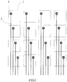
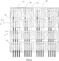
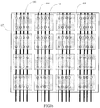
- At least one embodiment of the present disclosure provides an in-cell touch screen, as illustrated in Fig.2a to Fig.2d , that comprises: an upper substrate 100 and a lower substrate 200 that are provided opposite to each other, a plurality of mutually independent self-capacitance electrodes 01 located on a side, facing the lower substrate 200, of the upper substrate 100 or on a side, facing the upper substrate 100, of the lower substrate 200, wires 02 that are disposed on a different layer from the self-capacitance electrodes and electrically connected with respect to the self-capacitance electrodes 01, and an insulation layer 03 that is located between the self-capacitance electrodes 01 and the wires 02.
- the insulation layer 03 in an area that each self-capacitance electrode overlaps a wire 02, is provided with at least a first via hole 04 that runs through the insulation layer 03, with each self-capacitance electrode 01 being electrically connected to a corresponding wire 02 via a corresponding first via hole 04 and each wire 02 being electrically connected to a self-capacitance electrode 01; the each self-capacitance electrode 01, in an area overlapping other wire 02 than the corresponding wire 02 and at a position to which a first via hole 04 corresponds, is provided with a second via hole 05 that runs through a self-capacitance electrode 01, and an orthogonal projection of the second via hole 05 on a lower substrate 200 covers an orthogonal projection of the first vial hole 04 on the lower substrate.
- an insulation layer in an area that each self-capacitance electrode overlaps an wire, is provided with a first via hole that runs through the insulation layer, with each self-capacitance electrode being electrically connected with a corresponding wire via a corresponding first via hole; each self-capacitance electrode, within an area overlapping other wire than a corresponding wire and at a position corresponding to a first via hole, is disposed with a second via hole that runs through a self-capacitance electrode, with an orthogonal projection of a second via hole on a lower substrate covering an orthogonal projection of a first via hole on the lower substrate.
- the in-cell touch screen on the basis of ensuring that first via holes in an insulation layer of the in-cell touch screen are uniformly distributed, can also ensure that a wire is electrically connected with a corresponding self-capacitance electrode and other wires, except the one that is electrically connected with the corresponding self-capacitance electrode, are insulated from the self-capacitance electrode; therefore, on a basis that a self-capacitance electrode is connected with a wire correctly, it is able to solve a problem of uneven image display due to nonuniform distribution of via holes in an insulation layer.
- an insulation layer disposed between self-capacitance electrodes and wires, can include a plurality of film layers or one film layer, as long as the insulation layer can guarantee that self-capacitance electrodes and wires are insulated from each other, which will not be limited herein.
- the shapes and sizes of respective first via holes in an in-cell touch screen provided in at least one embodiment of the present disclosure can be the same.
- the shape of a first via hole, in an in-cell touch screen provided above in an embodiment of the present disclosure can be circular, rectangular or of any other geometric shapes, which will not be limited herein.
- the diameter of a first via hole 04, in an in-cell touch screen provided in at least one embodiment of the present disclosure can be less than the width of a wire 02 at a corresponding position.
- the thickness of a wire is usually greater than the thickness of a self-capacitance electrode, considering size deviation and alignment accuracy in manufacturing, for example, as illustrated in Fig.2c ,the diameter of a second via hole 05, in an in-cell touch screen provided in at least one embodiment of the present disclosure, can be less than the width of a wire 02 at a corresponding position.
- an in-cell touch screen provided in at least one embodiment of the present disclosure can further include: a conductive base block that is disposed on a same layer as the respective wire and corresponds to a first via hole. Because the thickness of a wire layer is greater than that of a self-capacitance electrode (a thickness of a self-capacitance electrode is 400-600 nm), deviation of the critical dimension of a wire layer is greater than that of an electrode layer, and an orthogonal projection of each conductive base block on an lower substrate covers an orthogonal projection of a second via hole on the lower substrate; each wire is connected with a corresponding self-capacitance electrode via a corresponding conductive base block.
- a conductive base block that is disposed on a same layer as the respective wire and corresponds to a first via hole.
- each wire 02 can extend in a same direction.
- the lengths of the wires 02 can be the same.
- a plurality of mutually independent self-capacitance electrodes 01 can be arranged in an array; wires 02 can extend in a column direction or a row direction.
- the arrangement rule of first via holes in areas that a self-capacitance electrode overlaps other wires than the wire that is electrically connected with the self-capacitance electrode is the same as that of the first via hole in an area that the self-capacitance electrode overlaps the wire that is electrically connected with the self-capacitance electrode.
- the distance of any two adjacent first via holes 04 having an overlapped area with the wire 02 is the same.
- a plurality of mutually independent self-capacitance electrodes are disposed on a same layer.
- patterns of all self-capacitance electrodes can be formed in one pattering process, hence simplifying process steps and saving fabrication cost.
- the self-capacitance electrodes can also be fabricated in layers, which will not be limited herein.
- an in-cell touch screen provided in any above embodiment of the present disclosure can be applied in a liquid crystal display screen of TN (Twisted Nematic) type, ADS (Advanced Dimension Switch) type, HADS (High-Advanced Dimension Switch) type or IPS (In-Plane Switch) type.
- TN Transmission Nematic
- ADS Advanced Dimension Switch
- HADS High-Advanced Dimension Switch
- IPS In-Plane Switch
- a common electrode layer with a plate structure is located below a slit-type pixel electrode, that is, a common electrode is provided between a lower substrate and a pixel electrode, and a passivation layer is further provided between the pixel electrode and the common electrode.
- a slit-type common electrode is located above a pixel electrode with a plate structure, that is, a pixel electrode is provided between an lower substrate and a common electrode, and a passivation layer is further provided between the pixel electrode an the common electrode.
- a way that a common electrode layer on a lower substrate is reused as a self-capacitance electrode can be employed, for example, the self-capacitance electrodes can collectively constitute a common electrode layer located on side facing, an upper substrate, of a lower substrate.
- an in-cell touch screen can further comprise a touch detection chip 210 that is configured to apply common electrode signals to respective self-capacitance electrodes in a display period and determine a touch position by detecting variation of capacitance value of each self-capacitance electrode in a touch period.
- a touch detection chip 210 that is configured to apply common electrode signals to respective self-capacitance electrodes in a display period and determine a touch position by detecting variation of capacitance value of each self-capacitance electrode in a touch period.
- each self-capacitance electrode is of a slit-type electrode structure (for example, ITO (indium tin oxide) electrode structure) or a plate-type electrode structure at a position corresponding to an aperture area of a pixel, that is, in a HADS mode, each self-capacitance electrode includes a slit-type electrode, for example, the slit-type electrode structure is an ITO electrode that has a slit in a pixel aperture area.
- a slit-type electrode structure for example, ITO (indium tin oxide) electrode structure
- the slit-type electrode structure is an ITO electrode that has a slit in a pixel aperture area.
- a plate-type electrode for example, an ITO electrode
- a portion, corresponding to a slit area of pixel electrodes, of a self-capacitance electrode interacts with a human electric field.
- the resolution of a touch screen is usually at a millimeter level, therefore, in a specific implementation, the density and occupied area of respective self-capacitance electrodes can be selected according to touch resolution needed to ensure required touch resolution, and each self-capacitance electrode is usually designed as a square electrode with a dimension of about 5*5mm.
- the resolution of a display screen is usually at a micrometer level, therefore, a self-capacitance electrode usually corresponds to a plurality of pixels in a display screen.
- a common electrode layer is reused as a self-capacitance electrode
- a mode that touch and display are driven in a time-sharing manner may be employed.
- a display drive chip and a touch detection chip can be integrated as one chip, so as to further reduce manufacturing cost.
- the time period of displaying each frame by a touch screen is divided into a display period and a touch period
- the time period of displaying one frame by a touch screen is 16.7 ms, in which 5 ms is selected as a touch period and rest 11.7 ms is selected as a display period; of course, the time duration of the two periods may also be adjusted according to processing capability of an IC chip, which will not be specifically limited herein.
- a gate scanning signal is applied on each gate electrode signal line (G1, G2 ⁇ Gn), gray level signals are applied on data signal lines D, and the touch detection chip that is connected with respective self-capacitance electrodes Cx1 ⁇ Cxn applies a common electrode signal on respective self-capacitance electrodes Cx1 ⁇ Cxn, thus realizing liquid crystal display function.
- an touch detection chip that is connected with respective self-capacitance electrodes Cx1 ⁇ Cxn applies a drive signal on each self-capacitance electrode Cx1 ⁇ Cxn simultaneously and meanwhile, receives feedback signal of the respective self-capacitance electrodes Cx1 ⁇ Cxn simultaneously; or as illustrated in Fig.4b , an touch detection chip that is connected with respective self-capacitance electrodes Cx1 ⁇ Cxn applies a drive signal on the respective self-capacitance electrodes Cx1 ⁇ Cxn in sequence and receives feedback signal of the respective self-capacitance electrodes Cx1 ⁇ Cxn respectively, which is not limited herein. Whether a touch occurs or not can be determined by means of analysis of feedback signals to realize a touch function.
- an in-cell touch screen above provided in at least one embodiment of the present disclosure can further include: data lines located below self-capacitance electrodes.
- the wires and data lines are disposed on a same layer and made of a same material.
- the respective wires can be prepared on a same layer as data lines, which can be realized by modifying patterns of the corresponding film layer without adding a new extra fabrication process, therefore, achieving a goal of simplifying process steps, saving manufacturing cost and improving manufacturing efficiency.
- the second via hole will not influence defection of a liquid crystal molecular regardless of its influence on the surrounding electric field, this is because in a display period what is transmitted over a wire is a common electrode voltage, and the voltage at the position of a second via hole of a self-capacitance electrode can be complemented by the common voltage over a wire, alleviating influence produced by a second via hole and ensuring uniformity of image display.
- an in-cell touch screen provided in at least one embodiment of the present disclosure can further include: a black matrix layer 110 located either on a side, facing an upper substrate 100, of a lower substrate 200 or on a side, facing a lower substrate 200, of an upper substrate 100; an orthogonal projection of the pattern of respective wires 02 on a lower substrate 200 is located within an area where pattern of a black matrix layer 110 is located; or an orthogonal projection of the pattern of respective second via holes on the lower substrate 200 is located within the area where pattern of a black matrix layer 110 is located.
- a wire or a second via hole is designed between pixels on an upper row and pixels on a lower row, and at this position a black matrix layer is provided, and therefore the black matrix layer covers the second via hole, liquid crystal molecules that can not be defected normally can be covered below the black matrix layer, which can further alleviate influence produced by a second via hole so as to ensure uniformity of image display.
- a width of a wire at a position that a first via hole corresponds to is usually wider than a width thereof at other positions, which configuration is the same as that in a common technology in the related art and is not limited herein.
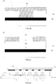
- an in-cell touch screen can include: a base substrate 10, and a gate electrode 11, a gate insulation layer 12, and an active layer 13 that are sequentially disposed on the base substrate 10, and a wire 02, a conductive base block 021, a source/drain electrode 14 and a data line 17 that are disposed on a same layer, and a pixel electrode layer 15, a passivation layer 16, and a common electrode layer 001 constitute a self-capacitance electrode 01.
- a first via hole 04 runs through a passivation layer 16, and a self-capacitance electrode 01 is electrically connected with a corresponding conductive base block 021 via a first via hole 04, so as to achieve an electrical connection of a self-capacitance electrode 01 and a corresponding wire 02.
- a self-capacitance electrode 01 at a position corresponding to a first via hole 04 is provided with a second via hole 05 that covers the first via hole 04, so as to guarantee that a self-capacitance electrode 01 at a position of a second via hole 05 is insulated from a conductive base block 021.
- any patterning process that is commonly used in the field can be employed to fabricate each film layer on a lower substrate, such as six patterning processes including: a patterning process for forming gate electrodes and gate lines; a patterning process for forming an active layer; a patterning process for forming wires, data lines and source/drain electrodes; a patterning process for forming pixel electrodes; a patterning process for forming a passivation layer; and a patterning process for forming a common electrode layer.
- six patterning processes including: a patterning process for forming gate electrodes and gate lines; a patterning process for forming an active layer; a patterning process for forming wires, data lines and source/drain electrodes; a patterning process for forming pixel electrodes; a patterning process for forming a passivation layer; and a patterning process for forming a common electrode layer.
- 6 patterning processes including: a patterning process for forming gate electrodes and gate lines; a patterning process for
- At least one embodiment of the present disclosure further provides a display device that includes an in-cell touch screen according to any above embodiment of the present disclosure.
- the display device can be any product or component having a display function such as a sell phone, a tablet computer, a TV set, a display, a laptop computer, a digital frame or a navigator.
- a display function such as a sell phone, a tablet computer, a TV set, a display, a laptop computer, a digital frame or a navigator.
- the implementation of the display device can be referred to the embodiment of the above in-cell touch screen; those redundant descriptions will not be explained here anymore.
- An in-cell touch screen and a display device are provided in the embodiments of the present disclosure.
- An insulation layer within an area that each self-capacitance electrode overlaps wires, is provided with at least a first via hole that runs through the insulation layer and each self-capacitance electrode is electrically connected with a corresponding wire via a corresponding first via hole.
- Each self-capacitance electrode within an area overlapping other wires than the wire that corresponds to itself and at a position that corresponds to a first via hole, is disposed with a second via hole that runs through a self-capacitance electrode, and a orthogonal projection of a second via hole on a lower substrate covers an orthogonal projection of a first via hole on the lower substrate.
- the in-cell touch screen on the basis of ensuring that first via holes are uniformly distributed in an insulation layer, can guarantee a corresponding wire is electrically connected with a self-capacitance electrode, and therefore, a self-capacitance electrode is insulated from the other wires than a corresponding wire that is electrically with the self-capacitance electrode.
- a self-capacitance electrode is insulated from the other wires than a corresponding wire that is electrically with the self-capacitance electrode.
Landscapes
- Engineering & Computer Science (AREA)
- General Engineering & Computer Science (AREA)
- Theoretical Computer Science (AREA)
- Human Computer Interaction (AREA)
- Physics & Mathematics (AREA)
- General Physics & Mathematics (AREA)
- Computer Networks & Wireless Communication (AREA)
- Position Input By Displaying (AREA)
Applications Claiming Priority (2)
| Application Number | Priority Date | Filing Date | Title |
|---|---|---|---|
| CN201510012621.6A CN104503648B (zh) | 2015-01-09 | 2015-01-09 | 一种内嵌式触摸屏及显示装置 |
| PCT/CN2015/087768 WO2016110104A1 (zh) | 2015-01-09 | 2015-08-21 | 内嵌式触摸屏及显示装置 |
Publications (3)
| Publication Number | Publication Date |
|---|---|
| EP3244292A1 true EP3244292A1 (de) | 2017-11-15 |
| EP3244292A4 EP3244292A4 (de) | 2018-07-25 |
| EP3244292B1 EP3244292B1 (de) | 2019-07-03 |
Family
ID=52945049
Family Applications (1)
| Application Number | Title | Priority Date | Filing Date |
|---|---|---|---|
| EP15876607.1A Active EP3244292B1 (de) | 2015-01-09 | 2015-08-21 | Berührungsbildschirm in der zelle und anzeigevorrichtung |
Country Status (4)
| Country | Link |
|---|---|
| US (1) | US10191599B2 (de) |
| EP (1) | EP3244292B1 (de) |
| CN (1) | CN104503648B (de) |
| WO (1) | WO2016110104A1 (de) |
Cited By (1)
| Publication number | Priority date | Publication date | Assignee | Title |
|---|---|---|---|---|
| CN111665999A (zh) * | 2020-07-29 | 2020-09-15 | 京东方科技集团股份有限公司 | 显示装置及其自容式触控面板 |
Families Citing this family (23)
| Publication number | Priority date | Publication date | Assignee | Title |
|---|---|---|---|---|
| WO2015180315A1 (zh) * | 2014-05-30 | 2015-12-03 | 京东方科技集团股份有限公司 | 电容式触摸结构、内嵌式触摸屏、显示装置及其扫描方法 |
| CN104503648B (zh) * | 2015-01-09 | 2017-06-09 | 京东方科技集团股份有限公司 | 一种内嵌式触摸屏及显示装置 |
| CN107765488B (zh) * | 2015-04-01 | 2019-12-31 | 上海天马微电子有限公司 | 阵列基板、触控显示面板和触控显示装置 |
| CN104965622B (zh) * | 2015-04-01 | 2018-09-28 | 上海天马微电子有限公司 | 阵列基板以及显示面板 |
| CN105138184B (zh) * | 2015-09-25 | 2018-06-22 | 深圳市华星光电技术有限公司 | 一种内嵌触摸液晶面板及其阵列基板 |
| CN105677076B (zh) | 2015-12-28 | 2018-09-25 | 上海天马微电子有限公司 | 触控显示装置、触控显示面板及阵列基板 |
| CN105607325B (zh) * | 2016-01-05 | 2018-09-04 | 京东方科技集团股份有限公司 | 触控屏及显示装置 |
| CN105629546A (zh) * | 2016-01-19 | 2016-06-01 | 深圳市华星光电技术有限公司 | 触摸面板以及其制造方法 |
| KR102701032B1 (ko) * | 2016-10-06 | 2024-09-03 | 삼성디스플레이 주식회사 | 터치 스크린 및 이를 구비한 표시 장치 |
| CN110249260B (zh) | 2017-02-15 | 2022-02-25 | 夏普株式会社 | 带位置输入功能的显示装置 |
| CN106909249B (zh) * | 2017-02-24 | 2020-06-09 | 厦门天马微电子有限公司 | 触控显示基板和触控显示装置 |
| JP6849501B2 (ja) * | 2017-03-29 | 2021-03-24 | 株式会社ジャパンディスプレイ | 表示装置 |
| JP2019053117A (ja) * | 2017-09-13 | 2019-04-04 | シャープ株式会社 | 位置入力機能付き表示装置 |
| JP2019053116A (ja) | 2017-09-13 | 2019-04-04 | シャープ株式会社 | 位置入力機能付き表示装置 |
| CN109976047B (zh) * | 2018-01-02 | 2021-03-16 | 京东方科技集团股份有限公司 | 触控电极结构、触控基板及制备方法、显示面板及装置 |
| US11099693B2 (en) | 2019-02-26 | 2021-08-24 | Beijing Boe Display Technology Co., Ltd. | Touch-sensing display substrate, touch-sensing display apparatus, method of operating touch-sensing display apparatus, and method of fabricating touch-sensing display substrate |
| CN110442255B (zh) * | 2019-02-26 | 2021-08-27 | 京东方科技集团股份有限公司 | 触控基板及触控显示装置 |
| US11106072B2 (en) * | 2019-02-27 | 2021-08-31 | Sharp Kabushiki Kaisha | Display device |
| CN110196521A (zh) * | 2019-05-30 | 2019-09-03 | 京东方科技集团股份有限公司 | 阵列基板及其制作方法、显示装置 |
| KR102792346B1 (ko) * | 2020-01-17 | 2025-04-09 | 삼성디스플레이 주식회사 | 표시 장치 |
| CN112198990B (zh) * | 2020-11-12 | 2024-01-30 | 武汉华星光电半导体显示技术有限公司 | 一种触控面板和显示装置 |
| KR102908990B1 (ko) * | 2021-12-31 | 2026-01-08 | 엘지디스플레이 주식회사 | 표시 장치 및 그의 제조 방법 |
| CN118860253B (zh) * | 2024-07-05 | 2025-01-28 | 深圳市宸金科技有限公司 | 一种用于远距离成像显示器的交互控制系统及方法 |
Family Cites Families (11)
| Publication number | Priority date | Publication date | Assignee | Title |
|---|---|---|---|---|
| TWI298613B (en) * | 2006-05-19 | 2008-07-01 | Foxconn Advanced Tech Inc | Method for manufacturing via holes used in printed circuit boards |
| CN102650916B (zh) * | 2011-02-25 | 2014-11-26 | 乐金显示有限公司 | 集成触摸传感器的显示设备 |
| JP2012221998A (ja) * | 2011-04-04 | 2012-11-12 | Toshiba Corp | 半導体装置ならびにその製造方法 |
| US9478590B2 (en) * | 2012-05-22 | 2016-10-25 | Superc-Touch Corporation | In-cell OLED touch display panel structure with metal layer for sensing |
| US9588368B2 (en) * | 2012-07-20 | 2017-03-07 | Shanghai Tianma Micro-electronics Co., Ltd. | Touch display panel |
| CN104022127B (zh) * | 2014-05-30 | 2016-10-05 | 京东方科技集团股份有限公司 | 一种阵列基板及其制作方法、以及显示装置 |
| CN104049800B (zh) * | 2014-05-30 | 2017-02-15 | 京东方科技集团股份有限公司 | 一种内嵌式触摸屏及显示装置 |
| CN104020893B (zh) * | 2014-05-30 | 2017-01-04 | 京东方科技集团股份有限公司 | 一种内嵌式触摸屏及显示装置 |
| CN104102402B (zh) * | 2014-06-25 | 2017-01-25 | 京东方科技集团股份有限公司 | 触控基板及显示装置 |
| CN104142772B (zh) * | 2014-07-24 | 2017-05-03 | 京东方科技集团股份有限公司 | 一种内嵌式触摸屏及显示装置 |
| CN104503648B (zh) * | 2015-01-09 | 2017-06-09 | 京东方科技集团股份有限公司 | 一种内嵌式触摸屏及显示装置 |
-
2015
- 2015-01-09 CN CN201510012621.6A patent/CN104503648B/zh active Active
- 2015-08-21 US US14/915,954 patent/US10191599B2/en active Active
- 2015-08-21 WO PCT/CN2015/087768 patent/WO2016110104A1/zh not_active Ceased
- 2015-08-21 EP EP15876607.1A patent/EP3244292B1/de active Active
Cited By (1)
| Publication number | Priority date | Publication date | Assignee | Title |
|---|---|---|---|---|
| CN111665999A (zh) * | 2020-07-29 | 2020-09-15 | 京东方科技集团股份有限公司 | 显示装置及其自容式触控面板 |
Also Published As
| Publication number | Publication date |
|---|---|
| EP3244292B1 (de) | 2019-07-03 |
| US20160216802A1 (en) | 2016-07-28 |
| WO2016110104A1 (zh) | 2016-07-14 |
| EP3244292A4 (de) | 2018-07-25 |
| CN104503648B (zh) | 2017-06-09 |
| US10191599B2 (en) | 2019-01-29 |
| CN104503648A (zh) | 2015-04-08 |
Similar Documents
| Publication | Publication Date | Title |
|---|---|---|
| EP3244292B1 (de) | Berührungsbildschirm in der zelle und anzeigevorrichtung | |
| US9665222B2 (en) | In-cell touch panel and display device with self-capacitance electrodes | |
| US9519374B2 (en) | In-cell touch panel and display device | |
| US10198130B2 (en) | In-cell touch panel and display device | |
| US10459573B2 (en) | In-cell touch panel and display device | |
| EP3153951B1 (de) | Eingebetteter berührungsbildschirm und anzeigevorrichtung | |
| US10031627B2 (en) | In-cell touch panel and display device | |
| US10013121B2 (en) | In-cell touch panel and display device with self-capacitance electrodes | |
| KR102020901B1 (ko) | 인-셀 터치 스크린 패널 및 디스플레이 디바이스 | |
| US9766761B2 (en) | In-cell touch panel and display device | |
| US10001870B2 (en) | In cell touch panel with uniformly-distributed grooves and display device | |
| US9830029B2 (en) | In-cell touch panel and display device | |
| US20160259445A1 (en) | Array substrate, method for fabricating the same and display device | |
| US9830028B2 (en) | In-cell touch panel with self-capacitive electrodes and display device | |
| US11042251B2 (en) | In-cell touch panel and display device | |
| KR20160145121A (ko) | 어레이 기판, 그 제조 방법 및 구동 방법, 및 디스플레이 디바이스 | |
| EP3270271B1 (de) | Zellintegrierter berührungsbildschirm und anzeigevorrichtung | |
| WO2015180356A1 (zh) | 电容式触摸结构、内嵌式触摸屏、显示装置及其扫描方法 |
Legal Events
| Date | Code | Title | Description |
|---|---|---|---|
| STAA | Information on the status of an ep patent application or granted ep patent |
Free format text: STATUS: THE INTERNATIONAL PUBLICATION HAS BEEN MADE |
|
| PUAI | Public reference made under article 153(3) epc to a published international application that has entered the european phase |
Free format text: ORIGINAL CODE: 0009012 |
|
| STAA | Information on the status of an ep patent application or granted ep patent |
Free format text: STATUS: REQUEST FOR EXAMINATION WAS MADE |
|
| 17P | Request for examination filed |
Effective date: 20161117 |
|
| AK | Designated contracting states |
Kind code of ref document: A1 Designated state(s): AL AT BE BG CH CY CZ DE DK EE ES FI FR GB GR HR HU IE IS IT LI LT LU LV MC MK MT NL NO PL PT RO RS SE SI SK SM TR |
|
| AX | Request for extension of the european patent |
Extension state: BA ME |
|
| DAV | Request for validation of the european patent (deleted) | ||
| DAX | Request for extension of the european patent (deleted) | ||
| REG | Reference to a national code |
Ref country code: DE Ref legal event code: R079 Ref document number: 602015033347 Country of ref document: DE Free format text: PREVIOUS MAIN CLASS: G06F0003044000 Ipc: G06F0003041000 |
|
| A4 | Supplementary search report drawn up and despatched |
Effective date: 20180622 |
|
| RIC1 | Information provided on ipc code assigned before grant |
Ipc: G06F 3/044 20060101ALI20180618BHEP Ipc: G06F 3/041 20060101AFI20180618BHEP |
|
| GRAP | Despatch of communication of intention to grant a patent |
Free format text: ORIGINAL CODE: EPIDOSNIGR1 |
|
| STAA | Information on the status of an ep patent application or granted ep patent |
Free format text: STATUS: GRANT OF PATENT IS INTENDED |
|
| INTG | Intention to grant announced |
Effective date: 20190121 |
|
| GRAS | Grant fee paid |
Free format text: ORIGINAL CODE: EPIDOSNIGR3 |
|
| GRAA | (expected) grant |
Free format text: ORIGINAL CODE: 0009210 |
|
| STAA | Information on the status of an ep patent application or granted ep patent |
Free format text: STATUS: THE PATENT HAS BEEN GRANTED |
|
| AK | Designated contracting states |
Kind code of ref document: B1 Designated state(s): AL AT BE BG CH CY CZ DE DK EE ES FI FR GB GR HR HU IE IS IT LI LT LU LV MC MK MT NL NO PL PT RO RS SE SI SK SM TR |
|
| REG | Reference to a national code |
Ref country code: GB Ref legal event code: FG4D |
|
| REG | Reference to a national code |
Ref country code: AT Ref legal event code: REF Ref document number: 1151768 Country of ref document: AT Kind code of ref document: T Effective date: 20190715 Ref country code: CH Ref legal event code: EP |
|
| REG | Reference to a national code |
Ref country code: IE Ref legal event code: FG4D |
|
| REG | Reference to a national code |
Ref country code: DE Ref legal event code: R096 Ref document number: 602015033347 Country of ref document: DE |
|
| REG | Reference to a national code |
Ref country code: NL Ref legal event code: FP |
|
| REG | Reference to a national code |
Ref country code: LT Ref legal event code: MG4D |
|
| REG | Reference to a national code |
Ref country code: AT Ref legal event code: MK05 Ref document number: 1151768 Country of ref document: AT Kind code of ref document: T Effective date: 20190703 |
|
| PG25 | Lapsed in a contracting state [announced via postgrant information from national office to epo] |
Ref country code: HR Free format text: LAPSE BECAUSE OF FAILURE TO SUBMIT A TRANSLATION OF THE DESCRIPTION OR TO PAY THE FEE WITHIN THE PRESCRIBED TIME-LIMIT Effective date: 20190703 Ref country code: BG Free format text: LAPSE BECAUSE OF FAILURE TO SUBMIT A TRANSLATION OF THE DESCRIPTION OR TO PAY THE FEE WITHIN THE PRESCRIBED TIME-LIMIT Effective date: 20191003 Ref country code: LT Free format text: LAPSE BECAUSE OF FAILURE TO SUBMIT A TRANSLATION OF THE DESCRIPTION OR TO PAY THE FEE WITHIN THE PRESCRIBED TIME-LIMIT Effective date: 20190703 Ref country code: SE Free format text: LAPSE BECAUSE OF FAILURE TO SUBMIT A TRANSLATION OF THE DESCRIPTION OR TO PAY THE FEE WITHIN THE PRESCRIBED TIME-LIMIT Effective date: 20190703 Ref country code: PT Free format text: LAPSE BECAUSE OF FAILURE TO SUBMIT A TRANSLATION OF THE DESCRIPTION OR TO PAY THE FEE WITHIN THE PRESCRIBED TIME-LIMIT Effective date: 20191104 Ref country code: AT Free format text: LAPSE BECAUSE OF FAILURE TO SUBMIT A TRANSLATION OF THE DESCRIPTION OR TO PAY THE FEE WITHIN THE PRESCRIBED TIME-LIMIT Effective date: 20190703 Ref country code: NO Free format text: LAPSE BECAUSE OF FAILURE TO SUBMIT A TRANSLATION OF THE DESCRIPTION OR TO PAY THE FEE WITHIN THE PRESCRIBED TIME-LIMIT Effective date: 20191003 Ref country code: FI Free format text: LAPSE BECAUSE OF FAILURE TO SUBMIT A TRANSLATION OF THE DESCRIPTION OR TO PAY THE FEE WITHIN THE PRESCRIBED TIME-LIMIT Effective date: 20190703 Ref country code: CZ Free format text: LAPSE BECAUSE OF FAILURE TO SUBMIT A TRANSLATION OF THE DESCRIPTION OR TO PAY THE FEE WITHIN THE PRESCRIBED TIME-LIMIT Effective date: 20190703 |
|
| PG25 | Lapsed in a contracting state [announced via postgrant information from national office to epo] |
Ref country code: ES Free format text: LAPSE BECAUSE OF FAILURE TO SUBMIT A TRANSLATION OF THE DESCRIPTION OR TO PAY THE FEE WITHIN THE PRESCRIBED TIME-LIMIT Effective date: 20190703 Ref country code: IS Free format text: LAPSE BECAUSE OF FAILURE TO SUBMIT A TRANSLATION OF THE DESCRIPTION OR TO PAY THE FEE WITHIN THE PRESCRIBED TIME-LIMIT Effective date: 20191103 Ref country code: LV Free format text: LAPSE BECAUSE OF FAILURE TO SUBMIT A TRANSLATION OF THE DESCRIPTION OR TO PAY THE FEE WITHIN THE PRESCRIBED TIME-LIMIT Effective date: 20190703 Ref country code: RS Free format text: LAPSE BECAUSE OF FAILURE TO SUBMIT A TRANSLATION OF THE DESCRIPTION OR TO PAY THE FEE WITHIN THE PRESCRIBED TIME-LIMIT Effective date: 20190703 Ref country code: GR Free format text: LAPSE BECAUSE OF FAILURE TO SUBMIT A TRANSLATION OF THE DESCRIPTION OR TO PAY THE FEE WITHIN THE PRESCRIBED TIME-LIMIT Effective date: 20191004 Ref country code: AL Free format text: LAPSE BECAUSE OF FAILURE TO SUBMIT A TRANSLATION OF THE DESCRIPTION OR TO PAY THE FEE WITHIN THE PRESCRIBED TIME-LIMIT Effective date: 20190703 |
|
| PG25 | Lapsed in a contracting state [announced via postgrant information from national office to epo] |
Ref country code: TR Free format text: LAPSE BECAUSE OF FAILURE TO SUBMIT A TRANSLATION OF THE DESCRIPTION OR TO PAY THE FEE WITHIN THE PRESCRIBED TIME-LIMIT Effective date: 20190703 |
|
| PG25 | Lapsed in a contracting state [announced via postgrant information from national office to epo] |
Ref country code: RO Free format text: LAPSE BECAUSE OF FAILURE TO SUBMIT A TRANSLATION OF THE DESCRIPTION OR TO PAY THE FEE WITHIN THE PRESCRIBED TIME-LIMIT Effective date: 20190703 Ref country code: EE Free format text: LAPSE BECAUSE OF FAILURE TO SUBMIT A TRANSLATION OF THE DESCRIPTION OR TO PAY THE FEE WITHIN THE PRESCRIBED TIME-LIMIT Effective date: 20190703 Ref country code: DK Free format text: LAPSE BECAUSE OF FAILURE TO SUBMIT A TRANSLATION OF THE DESCRIPTION OR TO PAY THE FEE WITHIN THE PRESCRIBED TIME-LIMIT Effective date: 20190703 Ref country code: PL Free format text: LAPSE BECAUSE OF FAILURE TO SUBMIT A TRANSLATION OF THE DESCRIPTION OR TO PAY THE FEE WITHIN THE PRESCRIBED TIME-LIMIT Effective date: 20190703 Ref country code: IT Free format text: LAPSE BECAUSE OF FAILURE TO SUBMIT A TRANSLATION OF THE DESCRIPTION OR TO PAY THE FEE WITHIN THE PRESCRIBED TIME-LIMIT Effective date: 20190703 |
|
| PG25 | Lapsed in a contracting state [announced via postgrant information from national office to epo] |
Ref country code: SM Free format text: LAPSE BECAUSE OF FAILURE TO SUBMIT A TRANSLATION OF THE DESCRIPTION OR TO PAY THE FEE WITHIN THE PRESCRIBED TIME-LIMIT Effective date: 20190703 Ref country code: MC Free format text: LAPSE BECAUSE OF FAILURE TO SUBMIT A TRANSLATION OF THE DESCRIPTION OR TO PAY THE FEE WITHIN THE PRESCRIBED TIME-LIMIT Effective date: 20190703 Ref country code: LU Free format text: LAPSE BECAUSE OF NON-PAYMENT OF DUE FEES Effective date: 20190821 Ref country code: IS Free format text: LAPSE BECAUSE OF FAILURE TO SUBMIT A TRANSLATION OF THE DESCRIPTION OR TO PAY THE FEE WITHIN THE PRESCRIBED TIME-LIMIT Effective date: 20200224 Ref country code: SK Free format text: LAPSE BECAUSE OF FAILURE TO SUBMIT A TRANSLATION OF THE DESCRIPTION OR TO PAY THE FEE WITHIN THE PRESCRIBED TIME-LIMIT Effective date: 20190703 Ref country code: LI Free format text: LAPSE BECAUSE OF NON-PAYMENT OF DUE FEES Effective date: 20190831 Ref country code: CH Free format text: LAPSE BECAUSE OF NON-PAYMENT OF DUE FEES Effective date: 20190831 |
|
| REG | Reference to a national code |
Ref country code: BE Ref legal event code: MM Effective date: 20190831 |
|
| REG | Reference to a national code |
Ref country code: DE Ref legal event code: R097 Ref document number: 602015033347 Country of ref document: DE |
|
| PLBE | No opposition filed within time limit |
Free format text: ORIGINAL CODE: 0009261 |
|
| STAA | Information on the status of an ep patent application or granted ep patent |
Free format text: STATUS: NO OPPOSITION FILED WITHIN TIME LIMIT |
|
| PG2D | Information on lapse in contracting state deleted |
Ref country code: IS |
|
| PG25 | Lapsed in a contracting state [announced via postgrant information from national office to epo] |
Ref country code: IE Free format text: LAPSE BECAUSE OF NON-PAYMENT OF DUE FEES Effective date: 20190821 |
|
| 26N | No opposition filed |
Effective date: 20200603 |
|
| PG25 | Lapsed in a contracting state [announced via postgrant information from national office to epo] |
Ref country code: SI Free format text: LAPSE BECAUSE OF FAILURE TO SUBMIT A TRANSLATION OF THE DESCRIPTION OR TO PAY THE FEE WITHIN THE PRESCRIBED TIME-LIMIT Effective date: 20190703 Ref country code: BE Free format text: LAPSE BECAUSE OF NON-PAYMENT OF DUE FEES Effective date: 20190831 |
|
| PG25 | Lapsed in a contracting state [announced via postgrant information from national office to epo] |
Ref country code: CY Free format text: LAPSE BECAUSE OF FAILURE TO SUBMIT A TRANSLATION OF THE DESCRIPTION OR TO PAY THE FEE WITHIN THE PRESCRIBED TIME-LIMIT Effective date: 20190703 |
|
| PG25 | Lapsed in a contracting state [announced via postgrant information from national office to epo] |
Ref country code: MT Free format text: LAPSE BECAUSE OF FAILURE TO SUBMIT A TRANSLATION OF THE DESCRIPTION OR TO PAY THE FEE WITHIN THE PRESCRIBED TIME-LIMIT Effective date: 20190703 Ref country code: HU Free format text: LAPSE BECAUSE OF FAILURE TO SUBMIT A TRANSLATION OF THE DESCRIPTION OR TO PAY THE FEE WITHIN THE PRESCRIBED TIME-LIMIT; INVALID AB INITIO Effective date: 20150821 |
|
| PG25 | Lapsed in a contracting state [announced via postgrant information from national office to epo] |
Ref country code: MK Free format text: LAPSE BECAUSE OF FAILURE TO SUBMIT A TRANSLATION OF THE DESCRIPTION OR TO PAY THE FEE WITHIN THE PRESCRIBED TIME-LIMIT Effective date: 20190703 |
|
| PGFP | Annual fee paid to national office [announced via postgrant information from national office to epo] |
Ref country code: NL Payment date: 20250821 Year of fee payment: 11 |
|
| PGFP | Annual fee paid to national office [announced via postgrant information from national office to epo] |
Ref country code: DE Payment date: 20250819 Year of fee payment: 11 |
|
| PGFP | Annual fee paid to national office [announced via postgrant information from national office to epo] |
Ref country code: GB Payment date: 20250821 Year of fee payment: 11 |
|
| PGFP | Annual fee paid to national office [announced via postgrant information from national office to epo] |
Ref country code: FR Payment date: 20250829 Year of fee payment: 11 |