EP3244223B1 - Integrated circuit measurement system - Google Patents
Integrated circuit measurement system Download PDFInfo
- Publication number
- EP3244223B1 EP3244223B1 EP16742817.6A EP16742817A EP3244223B1 EP 3244223 B1 EP3244223 B1 EP 3244223B1 EP 16742817 A EP16742817 A EP 16742817A EP 3244223 B1 EP3244223 B1 EP 3244223B1
- Authority
- EP
- European Patent Office
- Prior art keywords
- detection
- electrical parameter
- integrated circuit
- circuit
- meter
- Prior art date
- Legal status (The legal status is an assumption and is not a legal conclusion. Google has not performed a legal analysis and makes no representation as to the accuracy of the status listed.)
- Active
Links
Images





Classifications
-
- G—PHYSICS
- G01—MEASURING; TESTING
- G01R—MEASURING ELECTRIC VARIABLES; MEASURING MAGNETIC VARIABLES
- G01R31/00—Arrangements for testing electric properties; Arrangements for locating electric faults; Arrangements for electrical testing characterised by what is being tested not provided for elsewhere
- G01R31/28—Testing of electronic circuits, e.g. by signal tracer
- G01R31/2851—Testing of integrated circuits [IC]
- G01R31/2884—Testing of integrated circuits [IC] using dedicated test connectors, test elements or test circuits on the IC under test
-
- G—PHYSICS
- G01—MEASURING; TESTING
- G01B—MEASURING LENGTH, THICKNESS OR SIMILAR LINEAR DIMENSIONS; MEASURING ANGLES; MEASURING AREAS; MEASURING IRREGULARITIES OF SURFACES OR CONTOURS
- G01B7/00—Measuring arrangements characterised by the use of electric or magnetic techniques
- G01B7/16—Measuring arrangements characterised by the use of electric or magnetic techniques for measuring the deformation in a solid, e.g. by resistance strain gauge
- G01B7/18—Measuring arrangements characterised by the use of electric or magnetic techniques for measuring the deformation in a solid, e.g. by resistance strain gauge using change in resistance
- G01B7/20—Measuring arrangements characterised by the use of electric or magnetic techniques for measuring the deformation in a solid, e.g. by resistance strain gauge using change in resistance formed by printed-circuit technique
-
- G—PHYSICS
- G01—MEASURING; TESTING
- G01R—MEASURING ELECTRIC VARIABLES; MEASURING MAGNETIC VARIABLES
- G01R27/00—Arrangements for measuring resistance, reactance, impedance, or electric characteristics derived therefrom
- G01R27/02—Measuring real or complex resistance, reactance, impedance, or other two-pole characteristics derived therefrom, e.g. time constant
- G01R27/08—Measuring resistance by measuring both voltage and current
-
- G—PHYSICS
- G01—MEASURING; TESTING
- G01R—MEASURING ELECTRIC VARIABLES; MEASURING MAGNETIC VARIABLES
- G01R31/00—Arrangements for testing electric properties; Arrangements for locating electric faults; Arrangements for electrical testing characterised by what is being tested not provided for elsewhere
- G01R31/28—Testing of electronic circuits, e.g. by signal tracer
-
- G—PHYSICS
- G01—MEASURING; TESTING
- G01R—MEASURING ELECTRIC VARIABLES; MEASURING MAGNETIC VARIABLES
- G01R31/00—Arrangements for testing electric properties; Arrangements for locating electric faults; Arrangements for electrical testing characterised by what is being tested not provided for elsewhere
- G01R31/28—Testing of electronic circuits, e.g. by signal tracer
- G01R31/2801—Testing of printed circuits, backplanes, motherboards, hybrid circuits or carriers for multichip packages [MCP]
-
- G—PHYSICS
- G01—MEASURING; TESTING
- G01R—MEASURING ELECTRIC VARIABLES; MEASURING MAGNETIC VARIABLES
- G01R31/00—Arrangements for testing electric properties; Arrangements for locating electric faults; Arrangements for electrical testing characterised by what is being tested not provided for elsewhere
- G01R31/28—Testing of electronic circuits, e.g. by signal tracer
- G01R31/317—Testing of digital circuits
- G01R31/3181—Functional testing
- G01R31/3183—Generation of test inputs, e.g. test vectors, patterns or sequences
Definitions
- the present disclosure relates to the field of electronics, and in particular, to an integrated circuit detection system.
- a printed circuit board integrates various integrated circuits (integrated circuit, IC) to implement a specific function.
- IC integrated circuit
- a detection technology that integrates board function detection and channel function detection is mainly used to detect, on the printed circuit board, a potential quality hazard of an integrated circuit.
- Detection software may be embedded in the printed circuit board. The embedded detection software actuates the printed circuit board, and a detection meter or the printed circuit board receives a detection result.
- a detection meter may actuate the printed circuit board, and the detection meter or the printed circuit board receives a detection result, so as to determine, by detecting a functional failure of the printed circuit board, whether an electrical parameter of the integrated circuit on the printed circuit board or in a specific channel of the printed circuit board is abnormal, and whether the potential quality hazard exists in the integrated circuit.
- the board is the printed circuit board. Detecting an integrated circuit on a printed circuit board is referred to as on-board integrated circuit detection.
- EP2038720 relates to configurable voltage regulator.
- US 2013/0328588 relates to testing circuit and printed circuit board using same.
- US 2002/0125906 relates to method and semiconductor component having a device for determining an internal voltage.
- Implementations of the present disclosure provide an integrated circuit detection technique so as to detect an electrical parameter of an integrated circuit on a printed circuit board in a power-on state.
- a detection circuit connected to an integrated circuit on a printed circuit board is disposed on the printed circuit board, and an electrical parameter of the integrated circuit connected to the detection circuit is detected by using the detection circuit, so as to determine, according to a first electrical parameter, whether the electrical parameter of the integrated circuit connected to the detection circuit is normal.
- the claimed invention is directed to a system described in conjunction with figure 11 .
- the printed circuit board used in this invention has been described in implementation 1 below with reference to figures 1 - 3 and the detection apparatus has been described in implementation 2 below with reference to figures 4 and 5 .
- the method explained in conjunction with figures 6 and 7A-7C has not been claimed as such but is useful for understanding the operation of the claimed system.
- the printed circuit board 10 includes:
- N detection circuits 101 where each detection circuit is connected to a different integrated circuit 102, the detection circuit is provided with a first detection point a and a second detection point b, and the detection circuit is configured to detect an electrical parameter of the integrated circuit connected to the detection circuit; and N is an integer greater than or equal to 1.
- the first detection point and the second detection point are connected to a detection meter that is configured to perform electrical parameter detection, so that the detection meter obtains a first electrical parameter by using the first detection point and the second detection point, and determines, according to the first electrical parameter, whether the electrical parameter of the integrated circuit connected to the detection circuit is normal.
- the electrical parameter includes at least one of a total current, an on-resistance, or a voltage.
- a detection circuit connected to an integrated circuit on a printed circuit board is disposed on the printed circuit board, and an electrical parameter of the integrated circuit connected to the detection circuit is detected by using the detection circuit, so as to determine, according to a first detection result, whether the electrical parameter of the integrated circuit connected to the detection circuit is normal.
- the first detection point a is connected to a volt current condenser VCC pin A of the printed circuit board, and the second detection point b is connected to a volt current condenser (Volt Current Condenser, VCC) pin B of the integrated circuit.
- VCC pin A is a volt current condenser pin of the printed circuit board that supplies power to the integrated circuit.
- the VCC pin A may be a pin of a circuit that is on the printed circuit board and that provides a power supply function, or a pin of an external volt current condenser that supplies power to the printed circuit board.
- the first detection point a is connected to a function pin C of the integrated circuit
- the second detection point b is connected to a peripheral circuit 103 of the integrated circuit.
- the printed circuit board integrates various circuits. Different circuits have different functions, and the circuits are also connected to each other.
- the peripheral circuit may be another circuit on the printed circuit board.
- the detection circuit includes at least one resistor, or at least one magnetic device, and the magnetic device is a bead or an inductor.
- the detection circuit includes one resistor, a first end of the resistor is the first detection point, and a second end of the resistor is the second detection point.
- the resistors may be connected in a serial connection manner, or in a parallel connection manner, or in a hybrid manner combining serial connection and parallel connection.
- the detection circuit includes one bead, a first end of the bead is the first detection point, and a second end of the bead is the second detection point.
- the beads may be connected in a serial connection manner, or in a parallel connection manner, or in a hybrid manner combining serial connection and parallel connection.
- the detection circuit includes one inductor, a first end of the inductor is the first detection point, and a second end of the inductor is the second detection point.
- the detection circuit includes at least two inductors, the inductors may be connected in a serial connection manner, or in a parallel connection manner, or in a hybrid manner combining serial connection and parallel connection.
- the detection apparatus 20 includes:
- a detection control module of a detection apparatus controls a detection meter to detect a detection circuit that is disposed on a printed circuit board and that is connected to an integrated circuit on the printed circuit board, and to detect, by using the detection circuit, an electrical parameter of the integrated circuit connected to the detection circuit, so as to determine, according to a first detection result, whether the electrical parameter of the integrated circuit connected to the detection circuit is normal.
- the detection data processing module 203 is specifically configured to:
- the detection control module 201 is further configured to control the detection meter to connect to a function pin and a volt current condenser pin that are of the integrated circuit, or a function pin and a ground pin that are of the integrated circuit, that is, control the detection meter to connect to the function pin and the volt current condenser pin that are of the integrated circuit, or control the detection meter to connect to the function pin and the ground pin that are of the integrated circuit.
- the detection meter 202 is further configured to detect the integrated circuit to obtain a second detection result.
- the second detection result includes an electrical parameter of the function pin of the integrated circuit.
- the detection data processing module 203 is further configured to determine, according to the second detection result, whether the electrical parameter of the function pin of the integrated circuit is normal.
- the detection data processing module 203 is specifically configured to:
- the detection data processing module may include a data recording submodule 2031, a data analysis submodule 2032, and a warning submodule 2033.
- the data recording submodule is configured to record the first detection result and the second detection result.
- the data analysis submodule is configured to: determine whether the first detection result is within the first preset range; if the first detection result is within the first preset range, determine that the electrical parameter of the integrated circuit connected to the detection circuit is normal, or if the first detection result is not within the first preset range, determine that the electrical parameter of the integrated circuit connected to the detection circuit is abnormal; and determine whether the second detection result is within the second preset range, where the second preset range is the preset range of the electrical parameter of the function pin of the integrated circuit; and if the second detection result is within the second preset range, determine that the electrical parameter of the function pin of the integrated circuit is normal, or if the second detection result is not within the second preset range, determine that the electrical parameter of the function pin of the integrated circuit is abnormal.
- the warning submodule is configured to send, to user equipment, a warning prompt of the first detection result and/or the second detection result obtained by the data analysis submodule.
- the electrical parameter includes at least one of a total current, an on-resistance, or a voltage.
- a total current an on-resistance
- a voltage a voltage
- An implementation of the present disclosure provides an integrated circuit detection method, which is applied in the printed circuit board shown in FIG 1 and the detection apparatus shown in FIG 4 . As shown in FIG 6 , the method includes:
- the printed circuit board includes N detection circuits.
- Each detection circuit is connected to a different integrated circuit, the detection circuit is provided with the first detection point and the second detection point, and the detection circuit is configured to detect an electrical parameter of the integrated circuit connected to the detection circuit.
- N is an integer greater than or equal to 1.
- the first detection point and the second detection point are connected to the detection meter that is configured to perform electrical parameter detection, so that the detection meter obtains a first electrical parameter by using the first detection point and the second detection point, and a detection data processing module determines, according to the first electrical parameter, whether the electrical parameter of the integrated circuit connected to the detection circuit is normal.
- Step 303 The detection apparatus detects the detection circuit to obtain a first detection result, where the first detection result includes an electrical parameter of the integrated circuit connected to the detection circuit.
- the first detection result is a first electrical parameter.
- Step 304 The detection apparatus determines, according to the first detection result, whether the electrical parameter of the integrated circuit connected to the detection circuit is normal.
- a detection apparatus detects, by using a detection circuit, an electrical parameter of the integrated circuit connected to the detection circuit, and a detection circuit connected to the integrated circuit on a printed circuit board is disposed on the printed circuit board, so as to determine, according to a first detection result, whether the electrical parameter of the integrated circuit connected to the detection circuit is normal.
- An implementation of the present disclosure provides an integrated circuit detection method, which is applied in the printed circuit board shown in FIG 1 and the detection apparatus shown in FIG 4 .
- the detection apparatus further includes a data recording submodule, a data analysis submodule, and a warning submodule.
- the method includes: Step 401: The data recording submodule sets a detection information table.
- the detection information table may include a name of a printed circuit board, a batch number of an integrated circuit, a model of the integrated circuit, a detection start moment, and a detection end moment. In an actual application, information such as a detection meter model may be further set.
- Step 402 A detection control module sets a detection meter to a detection state.
- Step 403a The detection control module controls the detection meter to connect to a first detection point and a second detection point that are of an n th detection circuit.
- n is an integer greater than or equal to 1 and less than or equal to N, and N is an integer greater than or equal to 1.
- the n th detection circuit is a first detection circuit 502 on a printed circuit board 50.
- a first detection point a of the first detection circuit is connected to a volt current condenser VCC pin A of the printed circuit board, and a second detection point b of the first detection circuit 502 is connected to a volt current condenser VCC pin B of a first integrated circuit 501.
- a detection control module 512 in a detection apparatus 51 controls a detection meter 511 to separately connect to the first detection point a and the second detection point b, and the detection circuit 502 includes a resistor R1.
- FIG 8a is a specific circuit diagram of the detection system shown in FIG 8 .
- the first detection point a of the first detection circuit 502 is connected to a function pin C of the first integrated circuit 501, and the second detection point b of the first detection circuit 502 is connected to a peripheral circuit 503 of the first integrated circuit 501.
- the detection control module 512 in the detection apparatus 51 controls the detection meter 511 to separately connect to the first detection point a and the second detection point b, and the detection circuit 502 includes the resistor R1.
- Step 403b The detection control module controls the detection meter to connect to a function pin and a volt current condenser pin that are of an n th integrated circuit, or to connect to a function pin and a ground pin that are of an n th integrated circuit.
- the n th integrated circuit is the first integrated circuit 501 on the printed circuit board 50.
- the detection control module 512 in the detection apparatus 51 controls the detection meter 511 to connect to the function pin C and the volt current condenser pin VCC that are of the first integrated circuit 501, or to connect to the function pin C and the ground (Ground, GND) pin that are of the first integrated circuit 501.
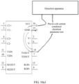
- FIG 10a 1 is a specific circuit diagram of the detection system shown in FIG 10a .
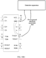
- FIG 10b 1 is a specific circuit diagram of the detection system shown in FIG 10b .
- Step 404a The detection meter detects the n th detection circuit to obtain a first detection result.
- the detection meter detects, by using the detection circuit, an electrical parameter of the n th integrated circuit to obtain the first detection result.
- the first detection result includes the electrical parameter of the integrated circuit connected to the detection circuit, and the electrical parameter may include at least one of a total current, an on-resistance, a voltage, or another electrical parameter of the integrated circuit connected to the detection circuit.
- Step 404b The detection meter detects the n th integrated circuit to obtain a second detection result.
- the detection meter first obtains detection results of the function pin and the volt current condenser pin that are of the n th integrated circuit and that are connected to the detection meter, then obtains detection results of the function pin and the ground pin that are of the n th integrated circuit and that are connected to the detection meter, and finally, comprehensively analyzes the detection results to obtain the second detection result.
- the second detection result includes an electrical parameter of the function pin of the integrated circuit, and the electrical parameter may include at least one of a total current, an on-resistance, a voltage, or another electrical parameter that is of the function pin of the integrated circuit.
- Step 405 The data recording submodule reads the first detection result or the second detection result from the detection meter.
- the data recording submodule may receive an instruction that is used for reading the first detection result or the second detection result and that is sent by the detection control module, and the data recording submodule reads the first detection result or the second detection result from the detection meter according to the instruction that is used for reading the first detection result or the second detection result.
- Step 406 The data recording submodule stores the first detection result or the second detection result into the detection information table.
- Step 407a The data analysis submodule determines, according to the first detection result, whether an electrical parameter of the integrated circuit connected to the detection circuit is normal.
- the data analysis submodule determines whether the first detection result is within a first preset range.
- the first preset range is a preset range of the electrical parameter of the integrated circuit connected to the detection circuit. If the first detection result is within the first preset range, step 408a is performed; or if the first detection result is not within the first preset range, step 409a is performed.
- Step 407b The data analysis submodule determines, according to the second detection result, whether an electrical parameter of the function pin of the integrated circuit is normal.
- the data analysis submodule determines whether the second detection result is within a second preset range.
- the second preset range is a preset range of the electrical parameter of the function pin of the integrated circuit. If the second detection result is within the second preset range, step 408b is performed; or if the second detection result is not within the second preset range, step 409b is performed.
- Step 408a The data analysis submodule determines that the electrical parameter of the integrated circuit connected to the detection circuit is normal.
- Step 409a The data analysis submodule determines that the electrical parameter of the integrated circuit connected to the detection circuit is abnormal.
- Step 408b The data analysis submodule determines that the electrical parameter of the function pin of the integrated circuit is normal.
- Step 409b The data analysis submodule determines that the electrical parameter of the function pin of the integrated circuit is abnormal.
- Step 4010 The warning submodule sends a warning prompt to user equipment.
- the warning submodule sends, to the user equipment, the warning prompt of a detection result obtained by the data analysis submodule.
- the warning prompt may be automatically sent to a mailbox, a mobile phone, or another terminal by using a network.
- a link to a to-be-analyzed problem ticket that is automatically created is pushed to the terminal together with the warning prompt. If the to-be-analyzed problem ticket is not handled, the warning submodule automatically sends the warning prompt periodically according to a preset time.
- Step 4011 The detection control module determines whether the n th integrated circuit is an N th integrated circuit.
- step 4012 is performed; or if n th integrated circuit is not the N th integrated circuit, step 4013 is performed.
- Step 4012 The detection control module sets the detection meter to a non-detection state.
- Step 4013 The detection control module controls the detection meter to connect to a first detection point and a second detection point that are of an (n+1) th detection circuit.
- a detection apparatus detects, by using a detection circuit, an electrical parameter of the integrated circuit connected to the detection circuit, and a detection circuit connected to the integrated circuit on a printed circuit board is disposed on the printed circuit board, so as to determine, according to a first detection result, whether the electrical parameter of the integrated circuit connected to the detection circuit is normal; or the detection apparatus directly controls a detection meter to connect to a function pin and a volt current condenser pin that are of the integrated circuit, or to connect to a function pin and a ground pin that are of the integrated circuit for detecting an electrical parameter of the function pin of the integrated circuit, so as to determine, according to a second detection result, whether the electrical parameter of the function pin of the integrated circuit is normal.
- integrated circuits on multiple printed circuit boards that are of a same type and of a same batch may be detected by using the integrated circuit detection method according to the present disclosure, so as to collect statistics on detection results of the same integrated circuits that are on the multiple printed circuit boards and that are obtained by detection, and to analyze whether any one of the integrated circuits on the printed circuit boards that are of the same type and of the same batch are abnormal.
- one model-J integrated circuit is used on a printed circuit board A.
- model-J integrated circuits with an abnormal electrical parameter may be identified by using methods such as a mean value method and a scatter chart and according to detection results of the 1000 model-J integrated circuits. Therefore, whether a potential quality problem occurs on model-J integrated circuits of a same batch or on an individual model-J integrated circuit can be identified according to a conclusion that is obtained by analyzing abnormal model-J integrated circuits. Likewise, if multiple model-J integrated circuits are used on the printed circuit board, abnormal model-J integrated circuits in different positions may be identified by using the method.
- printed circuit boards of different types and integrated circuits of different batches can be analyzed together, so as to effectively identify a potential quality hazard caused by an abnormal electrical parameter of an integrated circuit.
- one model-J integrated circuit is used on a printed circuit board A
- two model-J integrated circuits are used in different positions of a printed circuit board B
- 1000 printed circuit boards A and 1000 printed circuit boards B are processed.
- model-J integrated circuits in three positions are abnormal are separately determined first, and then three detection results are compared according to a preliminary conclusion, so as to analyze whether a model-J integrated circuit is abnormal.
- a conclusion obtained by using this method is more accurate than a conclusion that is obtained by means of identification based on a single position.
- physical analysis may be further performed on an individual integrated circuit with an abnormal detection result, so as to determine whether a potential quality hazard exists in integrated circuits of a same batch.
- the detection system 70 includes a printed circuit board 701 and a detection apparatus 702.
- the printed circuit board 701 includes N detection circuits 7011. Each detection circuit is connected to a different integrated circuit 7012.
- the detection circuit is provided with a first detection point a and a second detection point b, and the detection circuit is configured to detect an electrical parameter of the integrated circuit connected to the detection circuit.
- N is an integer greater than or equal to 1.
- the first detection point and the second detection point are connected to a detection meter that is configured to perform electrical parameter detection, so that the detection meter obtains a first electrical parameter by using the first detection point and the second detection point, and a detection data processing module determines, according to the first electrical parameter, whether the electrical parameter of the integrated circuit connected to the detection circuit is normal.
- the detection apparatus 702 includes:
- a detection apparatus detects, by using a detection circuit, an electrical parameter of the integrated circuit connected to the detection circuit, and a detection circuit connected to the integrated circuit on a printed circuit board is disposed on the printed circuit board, so as to determine, according to a first detection result, whether the electrical parameter of the integrated circuit connected to the detection circuit is normal; or the detection apparatus directly controls a detection meter to connect to a function pin and a volt current condenser pin that are of the integrated circuit, or to connect to a function pin and a ground pin that are of the integrated circuit for detecting an electrical parameter of the function pin of the integrated circuit, so as to determine, according to a second detection result, whether the electrical parameter of the function pin of the integrated circuit is normal.
- the power-on state includes a state in which the printed circuit board is powered on but no service is running on the printed circuit board, and a state in which the printed circuit board is powered on and a service is running on the printed circuit board.
- the N detection circuits included in the printed circuit board may be the same or may be different, and each detection circuit is connected to the different integrated circuit.
- the first detection result is a first electrical parameter
- the second detection result is a second electrical parameter
- the electrical parameter includes at least one of a total current, an on-resistance, or a voltage.
- a preset range of the electrical parameter of the integrated circuit connected to the detection circuit is a range of an empirical value obtained when the integrated circuit operates on the printed circuit board, or a range of a mean value obtained by performing a test.
- a preset range of the electrical parameter of the function pin of the integrated circuit is a range of an empirical value obtained when the integrated circuit operates on the printed circuit board, or a range of a mean value obtained by performing a test.
- the disclosed system, apparatus, and method may be implemented in other manners.
- the described apparatus implementation is merely an example.
- the module or unit division is merely logical function division and may be other division in actual implementation.
- a plurality of units or components may be combined or integrated into another system, or some features may be ignored or not performed.
- the displayed or discussed mutual couplings or direct couplings or communication connections may be implemented by using some interfaces.
- the indirect couplings or communication connections between the apparatuses or units may be implemented in electronic, mechanical, or other forms.
- the units described as separate parts may or may not be physically separate, and parts displayed as units may or may not be physical units, may be located in one position, or may be distributed on a plurality of network units. Some or all of the units may be selected according to actual needs to achieve the objectives of the solutions of the implementations.
- functional units in the implementations of the present disclosure may be integrated into one processing unit, or each of the units may exist alone physically, or two or more units are integrated into one unit.
- the integrated unit may be implemented in a form of hardware, or may be implemented in a form of a software functional unit.
- the integrated unit When the integrated unit is implemented in the form of a software functional unit and sold or used as an independent product, the integrated unit may be stored in a computer-readable storage medium. Based on such an understanding, the technical solutions of the present disclosure essentially, or the part contributing to the prior art, or all or a part of the technical solutions may be implemented in the form of a software product.
- the software product is stored in a storage medium and includes several instructions for instructing a computer device (which may be a personal computer, a server, or a network device) or a processor to perform all or a part of the steps of the methods described in the implementations of the present disclosure.
- the foregoing storage medium includes: any medium that can store program code, such as a USB flash drive, a removable hard disk, a read-only memory (ROM, Read-Only Memory), a random access memory (RAM, Random Access Memory), a magnetic disk, or an optical disc.
- program code such as a USB flash drive, a removable hard disk, a read-only memory (ROM, Read-Only Memory), a random access memory (RAM, Random Access Memory), a magnetic disk, or an optical disc.
Landscapes
- Engineering & Computer Science (AREA)
- Physics & Mathematics (AREA)
- General Physics & Mathematics (AREA)
- General Engineering & Computer Science (AREA)
- Computer Hardware Design (AREA)
- Microelectronics & Electronic Packaging (AREA)
- Tests Of Electronic Circuits (AREA)
- Testing Of Short-Circuits, Discontinuities, Leakage, Or Incorrect Line Connections (AREA)
Description
- The present disclosure relates to the field of electronics, and in particular, to an integrated circuit detection system.
- A printed circuit board (Printed Circuit Board, PCB) integrates various integrated circuits (integrated circuit, IC) to implement a specific function. Generally, a detection technology that integrates board function detection and channel function detection is mainly used to detect, on the printed circuit board, a potential quality hazard of an integrated circuit. Detection software may be embedded in the printed circuit board. The embedded detection software actuates the printed circuit board, and a detection meter or the printed circuit board receives a detection result. Alternatively, a detection meter may actuate the printed circuit board, and the detection meter or the printed circuit board receives a detection result, so as to determine, by detecting a functional failure of the printed circuit board, whether an electrical parameter of the integrated circuit on the printed circuit board or in a specific channel of the printed circuit board is abnormal, and whether the potential quality hazard exists in the integrated circuit. The board is the printed circuit board. Detecting an integrated circuit on a printed circuit board is referred to as on-board integrated circuit detection.
- However, in the prior art, only a functional failure of a printed circuit board or a channel-level functional failure of a printed circuit board can be detected, and a quality problem of a specific integrated circuit on the printed circuit board cannot be detected. Consequently, an electrical parameter of the integrated circuit cannot be accurately detected; when a function of the printed circuit board is normal, a potential quality hazard caused by an abnormal electrical parameter of the integrated circuit cannot be identified.
-
EP2038720 relates to configurable voltage regulator.US 2013/0328588 relates to testing circuit and printed circuit board using same. -
US 2002/0125906 relates to method and semiconductor component having a device for determining an internal voltage. - Implementations of the present disclosure provide an integrated circuit detection technique so as to detect an electrical parameter of an integrated circuit on a printed circuit board in a power-on state.
- To achieve the foregoing objective, the following technical solutions are used in the implementations of the present disclosure.
- The invention has been defined in the independent claim. Further specific technical features have been defined in the dependent claims.
- According to implementations of the present disclosure, a detection circuit connected to an integrated circuit on a printed circuit board is disposed on the printed circuit board, and an electrical parameter of the integrated circuit connected to the detection circuit is detected by using the detection circuit, so as to determine, according to a first electrical parameter, whether the electrical parameter of the integrated circuit connected to the detection circuit is normal. This resolves a problem, in the prior art, that the electrical parameter of the integrated circuit on the printed circuit board cannot be detected when the printed circuit board is in a power-on state, so that the electrical parameter of the integrated circuit on the printed circuit board in the power-on state can be effectively detected.
-
-
FIG 1 is a schematic structural diagram of a printed circuit board according to an implementation of the present disclosure; -
FIG 2 is a schematic structural diagram of another printed circuit board according to an implementation of the present disclosure; -
FIG 3 is a schematic structural diagram of still another printed circuit board according to an implementation of the present disclosure; -
FIG 4 is a schematic structural diagram of a detection apparatus according to an implementation of the present disclosure; -
FIG 5 is a schematic structural diagram of another detection apparatus according to an implementation of the present disclosure; -
FIG 6 is a flowchart of an integrated circuit detection method according to an implementation of the present disclosure; -
FIG 7A to FIG 7C are a flowchart of another integrated circuit detection method according to an implementation of the present disclosure; -
FIG 8 is a schematic diagram of a detection system according to an implementation of the present disclosure; -
FIG 8a is a schematic circuit diagram of the detection system according to an implementation of the present disclosure; -
FIG 9 is a schematic diagram of another detection system according to an implementation of the present disclosure; -
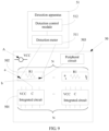
FIG 10 is a schematic diagram of still another detection system according to an implementation of the present disclosure; -
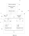
FIG 10a is a schematic diagram of a specific detection system shown inFIG 10 according to an implementation of the present disclosure; -
FIG 10a 1 is a schematic circuit diagram of the specific detection system shown inFIG 10a according to an implementation of the present disclosure; -
FIG 10b is a schematic diagram of the specific detection system shown inFIG 10 according to an implementation of the present disclosure; -
FIG 10b 1 is a schematic circuit diagram of the specific detection system shown inFIG 10b according to an implementation of the present disclosure; and -
FIG 11 is a schematic diagram of yet another detection system according to an implementation of the present disclosure. - To make the objectives, technical solutions, and advantages of this invention clearer, the following further describes various implementations in detail with reference to the accompanying drawings. The implementations described below are not all claimed, they are included to help understanding the context of the invention. While the description refers to various implementations, the embodiments of the invention are those which comprise at least all the features of the independent claim. Any implementation which does not fall within the scope of the claims does not form part of the invention, but rather included as an illustrative example that is useful for understanding the invention.
- In particular, the claimed invention is directed to a system described in conjunction with
figure 11 . The printed circuit board used in this invention has been described inimplementation 1 below with reference tofigures 1 - 3 and the detection apparatus has been described inimplementation 2 below with reference tofigures 4 and5 . The method explained in conjunction withfigures 6 and7A-7C has not been claimed as such but is useful for understanding the operation of the claimed system. - An implementation of the present disclosure provides a printed
circuit board 10. As shown inFIG 1 , the printedcircuit board 10 includes: -
N detection circuits 101, where each detection circuit is connected to a differentintegrated circuit 102, the detection circuit is provided with a first detection point a and a second detection point b, and the detection circuit is configured to detect an electrical parameter of the integrated circuit connected to the detection circuit; and N is an integer greater than or equal to 1. - The first detection point and the second detection point are connected to a detection meter that is configured to perform electrical parameter detection, so that the detection meter obtains a first electrical parameter by using the first detection point and the second detection point, and determines, according to the first electrical parameter, whether the electrical parameter of the integrated circuit connected to the detection circuit is normal. The electrical parameter includes at least one of a total current, an on-resistance, or a voltage.
- Therefore, a detection circuit connected to an integrated circuit on a printed circuit board is disposed on the printed circuit board, and an electrical parameter of the integrated circuit connected to the detection circuit is detected by using the detection circuit, so as to determine, according to a first detection result, whether the electrical parameter of the integrated circuit connected to the detection circuit is normal. This overcomes a problem, in the prior art, that the electrical parameter of the integrated circuit on the printed circuit board cannot be detected when the printed circuit board is in a power-on state, so that the electrical parameter of the integrated circuit on the printed circuit board in the power-on state can be effectively detected.
- A method for connecting the detection circuit and the integrated circuit is shown in
FIG 2 . The first detection point a is connected to a volt current condenser VCC pin A of the printed circuit board, and the second detection point b is connected to a volt current condenser (Volt Current Condenser, VCC) pin B of the integrated circuit. The VCC pin A is a volt current condenser pin of the printed circuit board that supplies power to the integrated circuit. For example, the VCC pin A may be a pin of a circuit that is on the printed circuit board and that provides a power supply function, or a pin of an external volt current condenser that supplies power to the printed circuit board. - As shown in
FIG 3 , the first detection point a is connected to a function pin C of the integrated circuit, and the second detection point b is connected to aperipheral circuit 103 of the integrated circuit. Generally, the printed circuit board integrates various circuits. Different circuits have different functions, and the circuits are also connected to each other. The peripheral circuit may be another circuit on the printed circuit board. - It should be noted that the detection circuit includes at least one resistor, or at least one magnetic device, and the magnetic device is a bead or an inductor. When the detection circuit includes one resistor, a first end of the resistor is the first detection point, and a second end of the resistor is the second detection point. When the detection circuit includes at least two resistors, the resistors may be connected in a serial connection manner, or in a parallel connection manner, or in a hybrid manner combining serial connection and parallel connection. Likewise, when the detection circuit includes one bead, a first end of the bead is the first detection point, and a second end of the bead is the second detection point. When the detection circuit includes at least two beads, the beads may be connected in a serial connection manner, or in a parallel connection manner, or in a hybrid manner combining serial connection and parallel connection. When the detection circuit includes one inductor, a first end of the inductor is the first detection point, and a second end of the inductor is the second detection point. When the detection circuit includes at least two inductors, the inductors may be connected in a serial connection manner, or in a parallel connection manner, or in a hybrid manner combining serial connection and parallel connection.
- An implementation of the present disclosure provides a
detection apparatus 20. As shown inFIG 4 , thedetection apparatus 20 includes: - a
detection control module 201, configured to set a detection state of adetection meter 202, where the detection apparatus includes the detection meter; and - the
detection control module 201 is further configured to control the detection meter to connect to a first detection point and a second detection point that are of a detection circuit on a printed circuit board in a power-on state, where the printed circuit board includes N detection circuits, each detection circuit is connected to a different integrated circuit, the detection circuit is provided with the first detection point and the second detection point, and the detection circuit is configured to detect an electrical parameter of the integrated circuit connected to the detection circuit; and N is an integer greater than or equal to 1, where the first detection point and the second detection point are connected to the detection meter that is configured to perform electrical parameter detection, so that the detection meter obtains a first electrical parameter by using the first detection point and the second detection point, and a detection data processing module determines, according to the first electrical parameter, whether the electrical parameter of the integrated circuit connected to the detection circuit is normal; - the
detection meter 202, configured to detect the detection circuit to obtain a first detection result, where the first detection result includes the electrical parameter of the integrated circuit connected to the detection circuit; and - the detection
data processing module 203, configured to determine, - Therefore, a detection control module of a detection apparatus controls a detection meter to detect a detection circuit that is disposed on a printed circuit board and that is connected to an integrated circuit on the printed circuit board, and to detect, by using the detection circuit, an electrical parameter of the integrated circuit connected to the detection circuit, so as to determine, according to a first detection result, whether the electrical parameter of the integrated circuit connected to the detection circuit is normal. This overcomes a problem, in the prior art, that the electrical parameter of the integrated circuit on the printed circuit board cannot be detected when the printed circuit board is in a power-on state, so that the electrical parameter of the integrated circuit on the printed circuit board in the power-on state can be effectively detected.
- The detection
data processing module 203 is specifically configured to: - determine whether the first detection result is within a first preset range, where the first preset range is a preset range of the electrical parameter of the integrated circuit connected to the detection circuit; and
- if the first detection result is within the first preset range, determine that the electrical parameter of the integrated circuit connected to the detection circuit is normal; or
- if the first detection result is not within the first preset range, determine that the electrical parameter of the integrated circuit connected to the detection circuit is abnormal.
- The
detection control module 201 is further configured to control the detection meter to connect to a function pin and a volt current condenser pin that are of the integrated circuit, or a function pin and a ground pin that are of the integrated circuit, that is, control the detection meter to connect to the function pin and the volt current condenser pin that are of the integrated circuit, or control the detection meter to connect to the function pin and the ground pin that are of the integrated circuit. - The
detection meter 202 is further configured to detect the integrated circuit to obtain a second detection result. The second detection result includes an electrical parameter of the function pin of the integrated circuit. - The detection
data processing module 203 is further configured to determine, according to the second detection result, whether the electrical parameter of the function pin of the integrated circuit is normal. - The detection
data processing module 203 is specifically configured to: - determine whether the second detection result is within a second preset range, where the second preset range is a preset range of the electrical parameter of the function pin of the integrated circuit; and
- if the second detection result is within the second preset range, determine that the electrical parameter of the function pin of the integrated circuit is normal; or
- if the second detection result is not within the second preset range, determine that the electrical parameter of the function pin of the integrated circuit is abnormal.
- As shown in
FIG 5 , the detection data processing module may include adata recording submodule 2031, adata analysis submodule 2032, and awarning submodule 2033. The data recording submodule is configured to record the first detection result and the second detection result. The data analysis submodule is configured to: determine whether the first detection result is within the first preset range; if the first detection result is within the first preset range, determine that the electrical parameter of the integrated circuit connected to the detection circuit is normal, or if the first detection result is not within the first preset range, determine that the electrical parameter of the integrated circuit connected to the detection circuit is abnormal; and determine whether the second detection result is within the second preset range, where the second preset range is the preset range of the electrical parameter of the function pin of the integrated circuit; and if the second detection result is within the second preset range, determine that the electrical parameter of the function pin of the integrated circuit is normal, or if the second detection result is not within the second preset range, determine that the electrical parameter of the function pin of the integrated circuit is abnormal. The warning submodule is configured to send, to user equipment, a warning prompt of the first detection result and/or the second detection result obtained by the data analysis submodule. - It should be noted that the electrical parameter includes at least one of a total current, an on-resistance, or a voltage. For a specific description of some function modules in the detection apparatus provided in this implementation of the present disclosure, refer to corresponding content in method implementations, and details are not described in this implementation.
- An implementation of the present disclosure provides an integrated circuit detection method, which is applied in the printed circuit board shown in
FIG 1 and the detection apparatus shown inFIG 4 . As shown inFIG 6 , the method includes: - Step 301: The detection apparatus sets a detection state of a detection meter, where the detection apparatus includes the detection meter.
- Step 302: The detection apparatus is connected to a first detection point and a second detection point that are of a detection circuit on the printed circuit board in a power-on state.
- The printed circuit board includes N detection circuits., Each detection circuit is connected to a different integrated circuit, the detection circuit is provided with the first detection point and the second detection point, and the detection circuit is configured to detect an electrical parameter of the integrated circuit connected to the detection circuit. N is an integer greater than or equal to 1. The first detection point and the second detection point are connected to the detection meter that is configured to perform electrical parameter detection, so that the detection meter obtains a first electrical parameter by using the first detection point and the second detection point, and a detection data processing module determines, according to the first electrical parameter, whether the electrical parameter of the integrated circuit connected to the detection circuit is normal.
- Step 303: The detection apparatus detects the detection circuit to obtain a first detection result, where the first detection result includes an electrical parameter of the integrated circuit connected to the detection circuit. The first detection result is a first electrical parameter.
- Step 304: The detection apparatus determines, according to the first detection result, whether the electrical parameter of the integrated circuit connected to the detection circuit is normal.
- According to the integrated circuit detection method provided in this implementation of the present disclosure, a detection apparatus detects, by using a detection circuit, an electrical parameter of the integrated circuit connected to the detection circuit, and a detection circuit connected to the integrated circuit on a printed circuit board is disposed on the printed circuit board, so as to determine, according to a first detection result, whether the electrical parameter of the integrated circuit connected to the detection circuit is normal. This overcomes a problem, in the prior art, that the electrical parameter of the integrated circuit on the printed circuit board cannot be detected when the printed circuit board is in a power-on state, so that the electrical parameter of the integrated circuit on the printed circuit board in the power-on state can be effectively detected.
- An implementation of the present disclosure provides an integrated circuit detection method, which is applied in the printed circuit board shown in
FIG 1 and the detection apparatus shown inFIG 4 . The detection apparatus further includes a data recording submodule, a data analysis submodule, and a warning submodule. As shown inFIG 7A to FIG 7C , the method includes:
Step 401: The data recording submodule sets a detection information table. - The detection information table may include a name of a printed circuit board, a batch number of an integrated circuit, a model of the integrated circuit, a detection start moment, and a detection end moment. In an actual application, information such as a detection meter model may be further set.
- Step 402: A detection control module sets a detection meter to a detection state.
-
Step 403a: The detection control module controls the detection meter to connect to a first detection point and a second detection point that are of an nth detection circuit. - n is an integer greater than or equal to 1 and less than or equal to N, and N is an integer greater than or equal to 1.
- For example, as shown in
FIG 8 , it is assumed that the nth detection circuit is afirst detection circuit 502 on a printedcircuit board 50. A first detection point a of the first detection circuit is connected to a volt current condenser VCC pin A of the printed circuit board, and a second detection point b of thefirst detection circuit 502 is connected to a volt current condenser VCC pin B of a firstintegrated circuit 501. Adetection control module 512 in adetection apparatus 51 controls adetection meter 511 to separately connect to the first detection point a and the second detection point b, and thedetection circuit 502 includes a resistor R1.FIG 8a is a specific circuit diagram of the detection system shown inFIG 8 . - As shown in
FIG 9 , the first detection point a of thefirst detection circuit 502 is connected to a function pin C of the firstintegrated circuit 501, and the second detection point b of thefirst detection circuit 502 is connected to aperipheral circuit 503 of the firstintegrated circuit 501. Thedetection control module 512 in thedetection apparatus 51 controls thedetection meter 511 to separately connect to the first detection point a and the second detection point b, and thedetection circuit 502 includes the resistor R1. - Step 403b: The detection control module controls the detection meter to connect to a function pin and a volt current condenser pin that are of an nth integrated circuit, or to connect to a function pin and a ground pin that are of an nth integrated circuit.
- For example, as shown in
FIG 10 , it is assumed that the nth integrated circuit is the firstintegrated circuit 501 on the printedcircuit board 50. Thedetection control module 512 in thedetection apparatus 51 controls thedetection meter 511 to connect to the function pin C and the volt current condenser pin VCC that are of the firstintegrated circuit 501, or to connect to the function pin C and the ground (Ground, GND) pin that are of the firstintegrated circuit 501. - That is, as shown in
FIG 10a , thedetection meter 511 is controlled to connect to the function pin C and the volt current condenser pin VCC that are of the firstintegrated circuit 501.FIG 10a FIG 10a . - As shown in
FIG 10b , thedetection meter 511 is controlled to connect to the function pin C and the ground pin that are of theintegrated circuit 501.FIG 10b FIG 10b . -
Step 404a: The detection meter detects the nth detection circuit to obtain a first detection result. - The detection meter detects, by using the detection circuit, an electrical parameter of the nth integrated circuit to obtain the first detection result. The first detection result includes the electrical parameter of the integrated circuit connected to the detection circuit, and the electrical parameter may include at least one of a total current, an on-resistance, a voltage, or another electrical parameter of the integrated circuit connected to the detection circuit.
- Step 404b: The detection meter detects the nth integrated circuit to obtain a second detection result.
- The detection meter first obtains detection results of the function pin and the volt current condenser pin that are of the nth integrated circuit and that are connected to the detection meter, then obtains detection results of the function pin and the ground pin that are of the nth integrated circuit and that are connected to the detection meter, and finally, comprehensively analyzes the detection results to obtain the second detection result. The second detection result includes an electrical parameter of the function pin of the integrated circuit, and the electrical parameter may include at least one of a total current, an on-resistance, a voltage, or another electrical parameter that is of the function pin of the integrated circuit.
- Step 405: The data recording submodule reads the first detection result or the second detection result from the detection meter.
- The data recording submodule may receive an instruction that is used for reading the first detection result or the second detection result and that is sent by the detection control module, and the data recording submodule reads the first detection result or the second detection result from the detection meter according to the instruction that is used for reading the first detection result or the second detection result.
- Step 406: The data recording submodule stores the first detection result or the second detection result into the detection information table.
-
Step 407a: The data analysis submodule determines, according to the first detection result, whether an electrical parameter of the integrated circuit connected to the detection circuit is normal. - The data analysis submodule determines whether the first detection result is within a first preset range. The first preset range is a preset range of the electrical parameter of the integrated circuit connected to the detection circuit. If the first detection result is within the first preset range,
step 408a is performed; or if the first detection result is not within the first preset range,step 409a is performed. -
Step 407b: The data analysis submodule determines, according to the second detection result, whether an electrical parameter of the function pin of the integrated circuit is normal. - The data analysis submodule determines whether the second detection result is within a second preset range. The second preset range is a preset range of the electrical parameter of the function pin of the integrated circuit. If the second detection result is within the second preset range,
step 408b is performed; or if the second detection result is not within the second preset range,step 409b is performed. -
Step 408a: The data analysis submodule determines that the electrical parameter of the integrated circuit connected to the detection circuit is normal. -
Step 409a: The data analysis submodule determines that the electrical parameter of the integrated circuit connected to the detection circuit is abnormal. -
Step 408b: The data analysis submodule determines that the electrical parameter of the function pin of the integrated circuit is normal. -
Step 409b: The data analysis submodule determines that the electrical parameter of the function pin of the integrated circuit is abnormal. - Step 4010: The warning submodule sends a warning prompt to user equipment.
- The warning submodule sends, to the user equipment, the warning prompt of a detection result obtained by the data analysis submodule. The warning prompt may be automatically sent to a mailbox, a mobile phone, or another terminal by using a network. In addition, a link to a to-be-analyzed problem ticket that is automatically created is pushed to the terminal together with the warning prompt. If the to-be-analyzed problem ticket is not handled, the warning submodule automatically sends the warning prompt periodically according to a preset time.
- Step 4011: The detection control module determines whether the nth integrated circuit is an Nth integrated circuit.
- If the nth integrated circuit is the Nth integrated circuit,
step 4012 is performed; or if nth integrated circuit is not the Nth integrated circuit,step 4013 is performed. - Step 4012: The detection control module sets the detection meter to a non-detection state.
- Step 4013: The detection control module controls the detection meter to connect to a first detection point and a second detection point that are of an (n+1)th detection circuit.
- According to the integrated circuit detection method provided in this implementation of the present disclosure, a detection apparatus detects, by using a detection circuit, an electrical parameter of the integrated circuit connected to the detection circuit, and a detection circuit connected to the integrated circuit on a printed circuit board is disposed on the printed circuit board, so as to determine, according to a first detection result, whether the electrical parameter of the integrated circuit connected to the detection circuit is normal; or the detection apparatus directly controls a detection meter to connect to a function pin and a volt current condenser pin that are of the integrated circuit, or to connect to a function pin and a ground pin that are of the integrated circuit for detecting an electrical parameter of the function pin of the integrated circuit, so as to determine, according to a second detection result, whether the electrical parameter of the function pin of the integrated circuit is normal. This overcomes a problem, in the prior art, that the electrical parameter of the integrated circuit on the printed circuit board cannot be detected when the printed circuit board is in a power-on state, so that the electrical parameter of the integrated circuit on the printed circuit board in the power-on state can be effectively detected.
- It should be noted that integrated circuits on multiple printed circuit boards that are of a same type and of a same batch may be detected by using the integrated circuit detection method according to the present disclosure, so as to collect statistics on detection results of the same integrated circuits that are on the multiple printed circuit boards and that are obtained by detection, and to analyze whether any one of the integrated circuits on the printed circuit boards that are of the same type and of the same batch are abnormal. For example, one model-J integrated circuit is used on a printed circuit board A. In a process of processing 1000 printed circuit boards A of a same batch, because the model-J integrated circuit is located at the same position on each printed circuit board A, and peripheral circuits of the model-J integrated circuits are also the same, model-J integrated circuits with an abnormal electrical parameter may be identified by using methods such as a mean value method and a scatter chart and according to detection results of the 1000 model-J integrated circuits. Therefore, whether a potential quality problem occurs on model-J integrated circuits of a same batch or on an individual model-J integrated circuit can be identified according to a conclusion that is obtained by analyzing abnormal model-J integrated circuits. Likewise, if multiple model-J integrated circuits are used on the printed circuit board, abnormal model-J integrated circuits in different positions may be identified by using the method.
- In particular, printed circuit boards of different types and integrated circuits of different batches can be analyzed together, so as to effectively identify a potential quality hazard caused by an abnormal electrical parameter of an integrated circuit. For example, one model-J integrated circuit is used on a printed circuit board A, two model-J integrated circuits are used in different positions of a printed circuit board B, and 1000 printed circuit boards A and 1000 printed circuit boards B are processed. Whether model-J integrated circuits in three positions are abnormal are separately determined first, and then three detection results are compared according to a preliminary conclusion, so as to analyze whether a model-J integrated circuit is abnormal. A conclusion obtained by using this method is more accurate than a conclusion that is obtained by means of identification based on a single position. Certainly, physical analysis may be further performed on an individual integrated circuit with an abnormal detection result, so as to determine whether a potential quality hazard exists in integrated circuits of a same batch.
- An implementation of the present disclosure provides a
detection system 70. As shown inFIG 11 , thedetection system 70 includes a printedcircuit board 701 and adetection apparatus 702. - The printed
circuit board 701 includesN detection circuits 7011. Each detection circuit is connected to a differentintegrated circuit 7012. The detection circuit is provided with a first detection point a and a second detection point b, and the detection circuit is configured to detect an electrical parameter of the integrated circuit connected to the detection circuit. N is an integer greater than or equal to 1. The first detection point and the second detection point are connected to a detection meter that is configured to perform electrical parameter detection, so that the detection meter obtains a first electrical parameter by using the first detection point and the second detection point, and a detection data processing module determines, according to the first electrical parameter, whether the electrical parameter of the integrated circuit connected to the detection circuit is normal. - The
detection apparatus 702 includes: - a
detection control module 7021, configured to set a detection state of the detection meter, where the detection apparatus includes the detection meter; and - the
detection control module 7021 is further configured to control the detection meter to connect to the first detection point and the second detection point that are of the detection circuit on the printed circuit board in a power-on state, where the printed circuit board includes the N detection circuits, each detection circuit is connected to the different integrated circuit, the detection circuit is provided with the first detection point and the second detection point, and the detection circuit is configured to detect the electrical parameter of the integrated circuit connected to the detection circuit; and N is the integer greater than or equal to 1; - the
detection meter 7022, configured to detect the detection circuit to obtain a first detection result, where the first detection result includes the electrical parameter of the integrated circuit connected to the detection circuit; and - the detection
data processing module 7023, configured to determine, according to the first detection result, whether the electrical parameter of the integrated circuit connected to the detection circuit is normal. - According to the integrated circuit detection method provided in this implementation of the present disclosure, a detection apparatus detects, by using a detection circuit, an electrical parameter of the integrated circuit connected to the detection circuit, and a detection circuit connected to the integrated circuit on a printed circuit board is disposed on the printed circuit board, so as to determine, according to a first detection result, whether the electrical parameter of the integrated circuit connected to the detection circuit is normal; or the detection apparatus directly controls a detection meter to connect to a function pin and a volt current condenser pin that are of the integrated circuit, or to connect to a function pin and a ground pin that are of the integrated circuit for detecting an electrical parameter of the function pin of the integrated circuit, so as to determine, according to a second detection result, whether the electrical parameter of the function pin of the integrated circuit is normal. This overcomes a problem, in the prior art, that the electrical parameter of the integrated circuit on the printed circuit board cannot be detected when the printed circuit board is in a power-on state, so that the electrical parameter of the integrated circuit on the printed circuit board in the power-on state can be effectively detected.
- It should be noted that, in the present disclosure, the power-on state includes a state in which the printed circuit board is powered on but no service is running on the printed circuit board, and a state in which the printed circuit board is powered on and a service is running on the printed circuit board. In the present disclosure, the N detection circuits included in the printed circuit board may be the same or may be different, and each detection circuit is connected to the different integrated circuit.
- In the present disclosure, the first detection result is a first electrical parameter, and the second detection result is a second electrical parameter.
- Based on the foregoing implementations, the electrical parameter includes at least one of a total current, an on-resistance, or a voltage. A preset range of the electrical parameter of the integrated circuit connected to the detection circuit is a range of an empirical value obtained when the integrated circuit operates on the printed circuit board, or a range of a mean value obtained by performing a test. A preset range of the electrical parameter of the function pin of the integrated circuit is a range of an empirical value obtained when the integrated circuit operates on the printed circuit board, or a range of a mean value obtained by performing a test.
- The foregoing descriptions about implementation manners allow a person skilled in the art to understand that, for the purpose of convenient and brief description, division of the foregoing function modules is used as an example for illustration. In actual application, the foregoing functions can be allocated to different modules and implemented according to a requirement, that is, an inner structure of an apparatus is divided into different function modules to implement all or part of the functions described above. For a detailed working process of the foregoing system, apparatus, and unit, reference may be made to a corresponding process in the foregoing method implementations, and details are not described herein again.
- In the several implementations provided in this application, it should be understood that the disclosed system, apparatus, and method may be implemented in other manners. For example, the described apparatus implementation is merely an example. For example, the module or unit division is merely logical function division and may be other division in actual implementation. For example, a plurality of units or components may be combined or integrated into another system, or some features may be ignored or not performed. In addition, the displayed or discussed mutual couplings or direct couplings or communication connections may be implemented by using some interfaces. The indirect couplings or communication connections between the apparatuses or units may be implemented in electronic, mechanical, or other forms.
- The units described as separate parts may or may not be physically separate, and parts displayed as units may or may not be physical units, may be located in one position, or may be distributed on a plurality of network units. Some or all of the units may be selected according to actual needs to achieve the objectives of the solutions of the implementations.
- In addition, functional units in the implementations of the present disclosure may be integrated into one processing unit, or each of the units may exist alone physically, or two or more units are integrated into one unit. The integrated unit may be implemented in a form of hardware, or may be implemented in a form of a software functional unit.
- When the integrated unit is implemented in the form of a software functional unit and sold or used as an independent product, the integrated unit may be stored in a computer-readable storage medium. Based on such an understanding, the technical solutions of the present disclosure essentially, or the part contributing to the prior art, or all or a part of the technical solutions may be implemented in the form of a software product. The software product is stored in a storage medium and includes several instructions for instructing a computer device (which may be a personal computer, a server, or a network device) or a processor to perform all or a part of the steps of the methods described in the implementations of the present disclosure. The foregoing storage medium includes: any medium that can store program code, such as a USB flash drive, a removable hard disk, a read-only memory (ROM, Read-Only Memory), a random access memory (RAM, Random Access Memory), a magnetic disk, or an optical disc.
- The scope of protection shall be defined by the appended claims.
Claims (7)
- A detection system, comprising a printed circuit board (10) and a detection apparatus (20); wherein:
the printed circuit board (10) comprises:N detection circuits (101) and N integrated circuits (102), wherein each detection circuit is connected to a different integrated circuit (102), and the detection circuit is provided with a first detection point and a second detection point, and N is an integer greater than or equal to 1;wherein:the first detection point is connected to a volt current condenser of the printed circuit board that supplies power to the integrated circuit, and the second detection point is connected to a volt current condenser pin of the integrated circuit;the detection apparatus (20) comprises:a detection control module (201), a detection meter (202), and a detection data processing module (203); whereinthe detection control module is configured to set a detection state of the detection meter and the detection control module is further configured to control the detection meter to connect to the first detection point and the second detection point that are of the detection circuit on the printed circuit board in a power-on state, whereinwhen the first detection point and the second detection point are connected to the detection meter this is configured to perform electrical parameter detection, so that the detection meter obtains a first electrical parameter by using the first detection point and the second detection point, andwherein the detection meter is further configured to detect the detection circuit to obtain the first electrical parameter, wherein the first electrical parameter is the electrical parameter of the integrated circuit connected to the detection circuit; andthe detection data processing module is configured to determine, according to the first electrical parameter, whether the electrical parameter of the integrated circuit connected to the detection circuit is normal;wherein:the detection control module is further configured to: control the detection meter to connect to a function pin and a volt current condenser pin that are of the integrated circuit, or control the detection meter to connect to a function pin and a ground pin that are of the integrated circuit;the detection meter is further configured to detect the integrated circuit to obtain a second electrical parameter, wherein the second electrical parameter is an electrical parameter of the function pin of the integrated circuit; andthe detection data processing module is further configured to determine, according to the second electrical parameter, whether the electrical parameter of the function pin of the integrated circuit is normal. - The system according to claim 1, wherein the detection circuit comprises at least one resistor, or at least one bead, or at least one inductor.
- The system according to claim 2, wherein when the detection circuit comprises a resistor, a first end of the resistor is the first detection point, and a second end of the resistor is the second detection point.
- The system according to claim 2, wherein when the detection circuit comprises the bead or the inductor, a first end of the bead is the first detection point, and a second end of the bead is the second detection point.
- The system according to any one of the preceding claims, wherein the detection data processing module is specifically configured to:determine whether the first electrical parameter is within a first preset range, wherein the first preset range is a preset range of the electrical parameter of the integrated circuit connected to the detection circuit; andif the first electrical parameter is within the first preset range, determine that the electrical parameter of the integrated circuit connected to the detection circuit is normal; orif the first electrical parameter is not within the first preset range, determine that the electrical parameter of the integrated circuit connected to the detection circuit is abnormal.
- The system according to any one of the preceding claims, wherein the detection data processing module is specifically configured to:determine whether the second electrical parameter is within a second preset range, wherein the second preset range is a preset range of the electrical parameter of the function pin of the integrated circuit; andif the second electrical parameter is within the second preset range, determine that the electrical parameter of the function pin of the integrated circuit is normal; orif the second electrical parameter is not within the second preset range, determine that the electrical parameter of the function pin of the integrated circuit is abnormal.
- The system according to any one of the preceding claims, wherein the electrical parameter comprises at least one of a total current, an on-resistance, or a voltage.
Applications Claiming Priority (2)
| Application Number | Priority Date | Filing Date | Title |
|---|---|---|---|
| CN201510052924.0A CN104635141B (en) | 2015-01-30 | 2015-01-30 | A kind of integrated circuit detection method, apparatus and system |
| PCT/CN2016/073073 WO2016119755A1 (en) | 2015-01-30 | 2016-02-01 | Integrated circuit measurement method, device, and system |
Publications (3)
| Publication Number | Publication Date |
|---|---|
| EP3244223A1 EP3244223A1 (en) | 2017-11-15 |
| EP3244223A4 EP3244223A4 (en) | 2018-01-24 |
| EP3244223B1 true EP3244223B1 (en) | 2023-05-31 |
Family
ID=53214105
Family Applications (1)
| Application Number | Title | Priority Date | Filing Date |
|---|---|---|---|
| EP16742817.6A Active EP3244223B1 (en) | 2015-01-30 | 2016-02-01 | Integrated circuit measurement system |
Country Status (4)
| Country | Link |
|---|---|
| US (1) | US10466297B2 (en) |
| EP (1) | EP3244223B1 (en) |
| CN (1) | CN104635141B (en) |
| WO (1) | WO2016119755A1 (en) |
Families Citing this family (6)
| Publication number | Priority date | Publication date | Assignee | Title |
|---|---|---|---|---|
| CN104635141B (en) | 2015-01-30 | 2018-07-03 | 华为技术有限公司 | A kind of integrated circuit detection method, apparatus and system |
| CN108508343B (en) * | 2017-02-24 | 2022-06-07 | 北京普源精电科技有限公司 | A detection device and method for a printed circuit board |
| CN108288447A (en) * | 2017-12-28 | 2018-07-17 | 江西合力泰科技有限公司 | A kind of test method for SPI interface |
| CN108490344B (en) * | 2018-03-28 | 2020-05-22 | 电子科技大学 | A fault diagnosis method for analog circuits based on training sample optimization |
| EP4186732A4 (en) * | 2020-07-10 | 2023-11-15 | Shinry Technologies Co., Ltd. | Vehicle-mounted dc/dc bond strap detection circuit |
| CN117110847B (en) * | 2023-10-25 | 2024-01-05 | 珠海智锐科技有限公司 | Internal resistance test method, device and equipment for printed circuit board and storage medium |
Family Cites Families (16)
| Publication number | Priority date | Publication date | Assignee | Title |
|---|---|---|---|---|
| NL8801835A (en) * | 1988-07-20 | 1990-02-16 | Philips Nv | METHOD AND APPARATUS FOR TESTING MULTIPLE POWER CONNECTIONS OF AN INTEGRATED CIRCUIT ON A PRINT PANEL |
| JP2000019212A (en) * | 1998-07-06 | 2000-01-21 | Arata Denshi Kk | Substrate inspection method and apparatus |
| DE10110626B4 (en) * | 2001-03-06 | 2004-09-16 | Infineon Technologies Ag | Method and semiconductor component with a device for determining an internal voltage |
| US6717415B2 (en) * | 2002-02-05 | 2004-04-06 | Logicvision, Inc. | Circuit and method for determining the location of defect in a circuit |
| US7512504B2 (en) * | 2002-09-19 | 2009-03-31 | Marvell World Trade Ltd. | Testing system using configurable integrated circuit |
| CN2577288Y (en) | 2002-09-20 | 2003-10-01 | 联想(北京)有限公司 | Electric signal testing device |
| CN2629046Y (en) * | 2003-05-26 | 2004-07-28 | 系新科技股份有限公司 | Component test setup for printed circuit boards |
| JP2005100332A (en) | 2003-08-29 | 2005-04-14 | Kyodo Printing Co Ltd | Inspection / measurement method and inspection / measurement system for electrical characteristics of IC chip incorporated in contact IC card or IC module, and stabilized power supply used therefor |
| US7317324B2 (en) * | 2003-11-04 | 2008-01-08 | Canon Kabushiki Kaisha | Semiconductor integrated circuit testing device and method |
| JP5047282B2 (en) * | 2006-07-06 | 2012-10-10 | マーベル ワールド トレード リミテッド | Configurable voltage regulator |
| CN201215580Y (en) * | 2008-07-15 | 2009-04-01 | 上海宏测半导体科技有限公司 | Integrated circuit test system |
| US8860455B2 (en) * | 2010-12-24 | 2014-10-14 | Intel Corporation | Methods and systems to measure a signal on an integrated circuit die |
| US8933722B2 (en) * | 2011-08-31 | 2015-01-13 | Infineon Technologies Ag | Measuring device and a method for measuring a chip-to-chip-carrier connection |
| KR20130073515A (en) * | 2011-12-23 | 2013-07-03 | 삼성전기주식회사 | Semiconductor package and method of manufacturing semiconductor package |
| CN103472347A (en) * | 2012-06-08 | 2013-12-25 | 富泰华工业(深圳)有限公司 | Auxiliary testing circuit, chip with auxiliary testing circuit and circuit board with auxiliary testing circuit |
| CN104635141B (en) * | 2015-01-30 | 2018-07-03 | 华为技术有限公司 | A kind of integrated circuit detection method, apparatus and system |
-
2015
- 2015-01-30 CN CN201510052924.0A patent/CN104635141B/en not_active Expired - Fee Related
-
2016
- 2016-02-01 WO PCT/CN2016/073073 patent/WO2016119755A1/en not_active Ceased
- 2016-02-01 EP EP16742817.6A patent/EP3244223B1/en active Active
-
2017
- 2017-07-28 US US15/663,002 patent/US10466297B2/en active Active
Also Published As
| Publication number | Publication date |
|---|---|
| US20170328950A1 (en) | 2017-11-16 |
| BR112017016243A2 (en) | 2018-03-27 |
| WO2016119755A1 (en) | 2016-08-04 |
| CN104635141B (en) | 2018-07-03 |
| CN104635141A (en) | 2015-05-20 |
| US10466297B2 (en) | 2019-11-05 |
| EP3244223A1 (en) | 2017-11-15 |
| EP3244223A4 (en) | 2018-01-24 |
Similar Documents
| Publication | Publication Date | Title |
|---|---|---|
| US10466297B2 (en) | Detection points of a printed circuit board to determine electrical parameter of an integrated circuit | |
| CN106324475A (en) | Automatic test method and device for board card | |
| KR102412330B1 (en) | Circuitry to protect a test instrument | |
| US20190196441A1 (en) | Apparatus, method, and computer readable media for controlling machining parameters | |
| CN111210864A (en) | DDR chip testing method, device, equipment and computer readable storage medium | |
| US20150035541A1 (en) | Signal integrity test apparatus and method for testing signal integrity of electronic product | |
| US20140375346A1 (en) | Test control device and method for testing signal integrities of electronic product | |
| CN113655370B (en) | Method, device, system and related equipment for determining abnormal test working condition of chip | |
| US10060982B2 (en) | Detecting faults in motors and drives | |
| CN106841977A (en) | Board card testing method and system | |
| CN115123426A (en) | Apparatus and method for controlling mass of vehicle | |
| US20140244195A1 (en) | Testing system and method for video graphics array port | |
| CN116819280A (en) | Chip abnormality identification method and device based on ZPAT algorithm | |
| US20060023934A1 (en) | Component edge detecting method, component edge detecting program and component inspection apparatus | |
| CN110457187B (en) | TPC-E test method and test server capable of conveniently running based on backup test data | |
| US20080315892A1 (en) | Methods and apparatus using one or more supernodes when testing for shorts between nodes of a circuit assembly | |
| CN111552634A (en) | Method and device for testing front-end system and storage medium | |
| CN107944372B (en) | Method and device for identifying signal validity and computer storage medium | |
| TW201439558A (en) | Electronic apparatus, electro-static discharge detecting system and method thereof | |
| CN211264169U (en) | Automatic testing device for logic control unit | |
| CN104123278A (en) | Test data processing system and method | |
| CN111444981A (en) | Leakage current fault positioning device and method | |
| CN114816876A (en) | Automatic test system for server Redfish interface specification | |
| CN104101826A (en) | Electronic device, and electrostatic discharge test system and method | |
| CN104216810A (en) | Method and device for detecting hardware fault of intelligent handheld device |
Legal Events
| Date | Code | Title | Description |
|---|---|---|---|
| STAA | Information on the status of an ep patent application or granted ep patent |
Free format text: STATUS: THE INTERNATIONAL PUBLICATION HAS BEEN MADE |
|
| PUAI | Public reference made under article 153(3) epc to a published international application that has entered the european phase |
Free format text: ORIGINAL CODE: 0009012 |
|
| STAA | Information on the status of an ep patent application or granted ep patent |
Free format text: STATUS: REQUEST FOR EXAMINATION WAS MADE |
|
| 17P | Request for examination filed |
Effective date: 20170810 |
|
| AK | Designated contracting states |
Kind code of ref document: A1 Designated state(s): AL AT BE BG CH CY CZ DE DK EE ES FI FR GB GR HR HU IE IS IT LI LT LU LV MC MK MT NL NO PL PT RO RS SE SI SK SM TR |
|
| AX | Request for extension of the european patent |
Extension state: BA ME |
|
| A4 | Supplementary search report drawn up and despatched |
Effective date: 20171221 |
|
| RIC1 | Information provided on ipc code assigned before grant |
Ipc: G01R 31/28 20060101AFI20171215BHEP |
|
| DAV | Request for validation of the european patent (deleted) | ||
| DAX | Request for extension of the european patent (deleted) | ||
| STAA | Information on the status of an ep patent application or granted ep patent |
Free format text: STATUS: EXAMINATION IS IN PROGRESS |
|
| 17Q | First examination report despatched |
Effective date: 20210318 |
|
| GRAP | Despatch of communication of intention to grant a patent |
Free format text: ORIGINAL CODE: EPIDOSNIGR1 |
|
| STAA | Information on the status of an ep patent application or granted ep patent |
Free format text: STATUS: GRANT OF PATENT IS INTENDED |
|
| INTG | Intention to grant announced |
Effective date: 20230126 |
|
| GRAS | Grant fee paid |
Free format text: ORIGINAL CODE: EPIDOSNIGR3 |
|
| GRAA | (expected) grant |
Free format text: ORIGINAL CODE: 0009210 |
|
| STAA | Information on the status of an ep patent application or granted ep patent |
Free format text: STATUS: THE PATENT HAS BEEN GRANTED |
|
| AK | Designated contracting states |
Kind code of ref document: B1 Designated state(s): AL AT BE BG CH CY CZ DE DK EE ES FI FR GB GR HR HU IE IS IT LI LT LU LV MC MK MT NL NO PL PT RO RS SE SI SK SM TR |
|
| REG | Reference to a national code |
Ref country code: GB Ref legal event code: FG4D Ref country code: CH Ref legal event code: EP |
|
| REG | Reference to a national code |
Ref country code: DE Ref legal event code: R096 Ref document number: 602016079703 Country of ref document: DE |
|
| REG | Reference to a national code |
Ref country code: AT Ref legal event code: REF Ref document number: 1571227 Country of ref document: AT Kind code of ref document: T Effective date: 20230615 |
|
| REG | Reference to a national code |
Ref country code: IE Ref legal event code: FG4D |
|
| REG | Reference to a national code |
Ref country code: LT Ref legal event code: MG9D |
|
| REG | Reference to a national code |
Ref country code: NL Ref legal event code: MP Effective date: 20230531 |
|
| REG | Reference to a national code |
Ref country code: AT Ref legal event code: MK05 Ref document number: 1571227 Country of ref document: AT Kind code of ref document: T Effective date: 20230531 |
|
| PG25 | Lapsed in a contracting state [announced via postgrant information from national office to epo] |
Ref country code: SE Free format text: LAPSE BECAUSE OF FAILURE TO SUBMIT A TRANSLATION OF THE DESCRIPTION OR TO PAY THE FEE WITHIN THE PRESCRIBED TIME-LIMIT Effective date: 20230531 Ref country code: NO Free format text: LAPSE BECAUSE OF FAILURE TO SUBMIT A TRANSLATION OF THE DESCRIPTION OR TO PAY THE FEE WITHIN THE PRESCRIBED TIME-LIMIT Effective date: 20230831 Ref country code: ES Free format text: LAPSE BECAUSE OF FAILURE TO SUBMIT A TRANSLATION OF THE DESCRIPTION OR TO PAY THE FEE WITHIN THE PRESCRIBED TIME-LIMIT Effective date: 20230531 Ref country code: AT Free format text: LAPSE BECAUSE OF FAILURE TO SUBMIT A TRANSLATION OF THE DESCRIPTION OR TO PAY THE FEE WITHIN THE PRESCRIBED TIME-LIMIT Effective date: 20230531 |
|
| PG25 | Lapsed in a contracting state [announced via postgrant information from national office to epo] |
Ref country code: RS Free format text: LAPSE BECAUSE OF FAILURE TO SUBMIT A TRANSLATION OF THE DESCRIPTION OR TO PAY THE FEE WITHIN THE PRESCRIBED TIME-LIMIT Effective date: 20230531 Ref country code: PL Free format text: LAPSE BECAUSE OF FAILURE TO SUBMIT A TRANSLATION OF THE DESCRIPTION OR TO PAY THE FEE WITHIN THE PRESCRIBED TIME-LIMIT Effective date: 20230531 Ref country code: NL Free format text: LAPSE BECAUSE OF FAILURE TO SUBMIT A TRANSLATION OF THE DESCRIPTION OR TO PAY THE FEE WITHIN THE PRESCRIBED TIME-LIMIT Effective date: 20230531 Ref country code: LV Free format text: LAPSE BECAUSE OF FAILURE TO SUBMIT A TRANSLATION OF THE DESCRIPTION OR TO PAY THE FEE WITHIN THE PRESCRIBED TIME-LIMIT Effective date: 20230531 Ref country code: LT Free format text: LAPSE BECAUSE OF FAILURE TO SUBMIT A TRANSLATION OF THE DESCRIPTION OR TO PAY THE FEE WITHIN THE PRESCRIBED TIME-LIMIT Effective date: 20230531 Ref country code: IS Free format text: LAPSE BECAUSE OF FAILURE TO SUBMIT A TRANSLATION OF THE DESCRIPTION OR TO PAY THE FEE WITHIN THE PRESCRIBED TIME-LIMIT Effective date: 20230930 Ref country code: HR Free format text: LAPSE BECAUSE OF FAILURE TO SUBMIT A TRANSLATION OF THE DESCRIPTION OR TO PAY THE FEE WITHIN THE PRESCRIBED TIME-LIMIT Effective date: 20230531 Ref country code: GR Free format text: LAPSE BECAUSE OF FAILURE TO SUBMIT A TRANSLATION OF THE DESCRIPTION OR TO PAY THE FEE WITHIN THE PRESCRIBED TIME-LIMIT Effective date: 20230901 |
|
| PG25 | Lapsed in a contracting state [announced via postgrant information from national office to epo] |
Ref country code: FI Free format text: LAPSE BECAUSE OF FAILURE TO SUBMIT A TRANSLATION OF THE DESCRIPTION OR TO PAY THE FEE WITHIN THE PRESCRIBED TIME-LIMIT Effective date: 20230531 |
|
| PG25 | Lapsed in a contracting state [announced via postgrant information from national office to epo] |
Ref country code: SK Free format text: LAPSE BECAUSE OF FAILURE TO SUBMIT A TRANSLATION OF THE DESCRIPTION OR TO PAY THE FEE WITHIN THE PRESCRIBED TIME-LIMIT Effective date: 20230531 |
|
| PG25 | Lapsed in a contracting state [announced via postgrant information from national office to epo] |
Ref country code: SM Free format text: LAPSE BECAUSE OF FAILURE TO SUBMIT A TRANSLATION OF THE DESCRIPTION OR TO PAY THE FEE WITHIN THE PRESCRIBED TIME-LIMIT Effective date: 20230531 Ref country code: SK Free format text: LAPSE BECAUSE OF FAILURE TO SUBMIT A TRANSLATION OF THE DESCRIPTION OR TO PAY THE FEE WITHIN THE PRESCRIBED TIME-LIMIT Effective date: 20230531 Ref country code: RO Free format text: LAPSE BECAUSE OF FAILURE TO SUBMIT A TRANSLATION OF THE DESCRIPTION OR TO PAY THE FEE WITHIN THE PRESCRIBED TIME-LIMIT Effective date: 20230531 Ref country code: PT Free format text: LAPSE BECAUSE OF FAILURE TO SUBMIT A TRANSLATION OF THE DESCRIPTION OR TO PAY THE FEE WITHIN THE PRESCRIBED TIME-LIMIT Effective date: 20231002 Ref country code: EE Free format text: LAPSE BECAUSE OF FAILURE TO SUBMIT A TRANSLATION OF THE DESCRIPTION OR TO PAY THE FEE WITHIN THE PRESCRIBED TIME-LIMIT Effective date: 20230531 Ref country code: DK Free format text: LAPSE BECAUSE OF FAILURE TO SUBMIT A TRANSLATION OF THE DESCRIPTION OR TO PAY THE FEE WITHIN THE PRESCRIBED TIME-LIMIT Effective date: 20230531 Ref country code: CZ Free format text: LAPSE BECAUSE OF FAILURE TO SUBMIT A TRANSLATION OF THE DESCRIPTION OR TO PAY THE FEE WITHIN THE PRESCRIBED TIME-LIMIT Effective date: 20230531 |
|
| REG | Reference to a national code |
Ref country code: DE Ref legal event code: R097 Ref document number: 602016079703 Country of ref document: DE |
|
| PLBE | No opposition filed within time limit |
Free format text: ORIGINAL CODE: 0009261 |
|
| STAA | Information on the status of an ep patent application or granted ep patent |
Free format text: STATUS: NO OPPOSITION FILED WITHIN TIME LIMIT |
|
| PGFP | Annual fee paid to national office [announced via postgrant information from national office to epo] |
Ref country code: DE Payment date: 20240116 Year of fee payment: 9 |
|
| PG25 | Lapsed in a contracting state [announced via postgrant information from national office to epo] |
Ref country code: SI Free format text: LAPSE BECAUSE OF FAILURE TO SUBMIT A TRANSLATION OF THE DESCRIPTION OR TO PAY THE FEE WITHIN THE PRESCRIBED TIME-LIMIT Effective date: 20230531 |
|
| 26N | No opposition filed |
Effective date: 20240301 |
|
| PG25 | Lapsed in a contracting state [announced via postgrant information from national office to epo] |
Ref country code: SI Free format text: LAPSE BECAUSE OF FAILURE TO SUBMIT A TRANSLATION OF THE DESCRIPTION OR TO PAY THE FEE WITHIN THE PRESCRIBED TIME-LIMIT Effective date: 20230531 Ref country code: IT Free format text: LAPSE BECAUSE OF FAILURE TO SUBMIT A TRANSLATION OF THE DESCRIPTION OR TO PAY THE FEE WITHIN THE PRESCRIBED TIME-LIMIT Effective date: 20230531 |
|
| PG25 | Lapsed in a contracting state [announced via postgrant information from national office to epo] |
Ref country code: MC Free format text: LAPSE BECAUSE OF FAILURE TO SUBMIT A TRANSLATION OF THE DESCRIPTION OR TO PAY THE FEE WITHIN THE PRESCRIBED TIME-LIMIT Effective date: 20230531 |
|
| REG | Reference to a national code |
Ref country code: CH Ref legal event code: PL |
|
| PG25 | Lapsed in a contracting state [announced via postgrant information from national office to epo] |
Ref country code: LU Free format text: LAPSE BECAUSE OF NON-PAYMENT OF DUE FEES Effective date: 20240201 |
|
| PG25 | Lapsed in a contracting state [announced via postgrant information from national office to epo] |
Ref country code: CH Free format text: LAPSE BECAUSE OF NON-PAYMENT OF DUE FEES Effective date: 20240229 |
|
| GBPC | Gb: european patent ceased through non-payment of renewal fee |
Effective date: 20240201 |
|
| PG25 | Lapsed in a contracting state [announced via postgrant information from national office to epo] |
Ref country code: LU Free format text: LAPSE BECAUSE OF NON-PAYMENT OF DUE FEES Effective date: 20240201 Ref country code: CH Free format text: LAPSE BECAUSE OF NON-PAYMENT OF DUE FEES Effective date: 20240229 |
|
| PG25 | Lapsed in a contracting state [announced via postgrant information from national office to epo] |
Ref country code: BG Free format text: LAPSE BECAUSE OF FAILURE TO SUBMIT A TRANSLATION OF THE DESCRIPTION OR TO PAY THE FEE WITHIN THE PRESCRIBED TIME-LIMIT Effective date: 20230531 |
|
| PG25 | Lapsed in a contracting state [announced via postgrant information from national office to epo] |
Ref country code: BG Free format text: LAPSE BECAUSE OF FAILURE TO SUBMIT A TRANSLATION OF THE DESCRIPTION OR TO PAY THE FEE WITHIN THE PRESCRIBED TIME-LIMIT Effective date: 20230531 |
|
| REG | Reference to a national code |
Ref country code: BE Ref legal event code: MM Effective date: 20240229 |
|
| PG25 | Lapsed in a contracting state [announced via postgrant information from national office to epo] |
Ref country code: BE Free format text: LAPSE BECAUSE OF NON-PAYMENT OF DUE FEES Effective date: 20240229 |
|
| PG25 | Lapsed in a contracting state [announced via postgrant information from national office to epo] |
Ref country code: GB Free format text: LAPSE BECAUSE OF NON-PAYMENT OF DUE FEES Effective date: 20240201 |
|
| PG25 | Lapsed in a contracting state [announced via postgrant information from national office to epo] |
Ref country code: FR Free format text: LAPSE BECAUSE OF NON-PAYMENT OF DUE FEES Effective date: 20240229 |
|
| PG25 | Lapsed in a contracting state [announced via postgrant information from national office to epo] |
Ref country code: IE Free format text: LAPSE BECAUSE OF NON-PAYMENT OF DUE FEES Effective date: 20240201 |
|
| PG25 | Lapsed in a contracting state [announced via postgrant information from national office to epo] |
Ref country code: IE Free format text: LAPSE BECAUSE OF NON-PAYMENT OF DUE FEES Effective date: 20240201 Ref country code: GB Free format text: LAPSE BECAUSE OF NON-PAYMENT OF DUE FEES Effective date: 20240201 Ref country code: FR Free format text: LAPSE BECAUSE OF NON-PAYMENT OF DUE FEES Effective date: 20240229 Ref country code: BE Free format text: LAPSE BECAUSE OF NON-PAYMENT OF DUE FEES Effective date: 20240229 |
|
| PG25 | Lapsed in a contracting state [announced via postgrant information from national office to epo] |
Ref country code: CY Free format text: LAPSE BECAUSE OF FAILURE TO SUBMIT A TRANSLATION OF THE DESCRIPTION OR TO PAY THE FEE WITHIN THE PRESCRIBED TIME-LIMIT; INVALID AB INITIO Effective date: 20160201 |
|
| REG | Reference to a national code |
Ref country code: DE Ref legal event code: R119 Ref document number: 602016079703 Country of ref document: DE |
|
| PG25 | Lapsed in a contracting state [announced via postgrant information from national office to epo] |
Ref country code: HU Free format text: LAPSE BECAUSE OF FAILURE TO SUBMIT A TRANSLATION OF THE DESCRIPTION OR TO PAY THE FEE WITHIN THE PRESCRIBED TIME-LIMIT; INVALID AB INITIO Effective date: 20160201 |
|
| PG25 | Lapsed in a contracting state [announced via postgrant information from national office to epo] |
Ref country code: TR Free format text: LAPSE BECAUSE OF FAILURE TO SUBMIT A TRANSLATION OF THE DESCRIPTION OR TO PAY THE FEE WITHIN THE PRESCRIBED TIME-LIMIT Effective date: 20230531 |
|
| PG25 | Lapsed in a contracting state [announced via postgrant information from national office to epo] |
Ref country code: DE Free format text: LAPSE BECAUSE OF NON-PAYMENT OF DUE FEES Effective date: 20250902 |