EP3240021A1 - A method for fabricating a semiconductor structure - Google Patents
A method for fabricating a semiconductor structure Download PDFInfo
- Publication number
- EP3240021A1 EP3240021A1 EP17163839.8A EP17163839A EP3240021A1 EP 3240021 A1 EP3240021 A1 EP 3240021A1 EP 17163839 A EP17163839 A EP 17163839A EP 3240021 A1 EP3240021 A1 EP 3240021A1
- Authority
- EP
- European Patent Office
- Prior art keywords
- layer
- metal layer
- dielectric layer
- temperature
- planarization process
- Prior art date
- Legal status (The legal status is an assumption and is not a legal conclusion. Google has not performed a legal analysis and makes no representation as to the accuracy of the status listed.)
- Granted
Links
Images



Classifications
-
- H—ELECTRICITY
- H10—SEMICONDUCTOR DEVICES; ELECTRIC SOLID-STATE DEVICES NOT OTHERWISE PROVIDED FOR
- H10D—INORGANIC ELECTRIC SEMICONDUCTOR DEVICES
- H10D64/00—Electrodes of devices having potential barriers
- H10D64/01—Manufacture or treatment
- H10D64/013—Manufacture or treatment of electrodes having a conductor capacitively coupled to a semiconductor by an insulator
- H10D64/01302—Manufacture or treatment of electrodes having a conductor capacitively coupled to a semiconductor by an insulator the insulator being formed after the semiconductor body, the semiconductor being silicon
- H10D64/01304—Manufacture or treatment of electrodes having a conductor capacitively coupled to a semiconductor by an insulator the insulator being formed after the semiconductor body, the semiconductor being silicon characterised by the conductor
- H10D64/01326—Aspects related to lithography, isolation or planarisation of the conductor
-
- H—ELECTRICITY
- H10—SEMICONDUCTOR DEVICES; ELECTRIC SOLID-STATE DEVICES NOT OTHERWISE PROVIDED FOR
- H10D—INORGANIC ELECTRIC SEMICONDUCTOR DEVICES
- H10D64/00—Electrodes of devices having potential barriers
- H10D64/01—Manufacture or treatment
- H10D64/013—Manufacture or treatment of electrodes having a conductor capacitively coupled to a semiconductor by an insulator
- H10D64/01302—Manufacture or treatment of electrodes having a conductor capacitively coupled to a semiconductor by an insulator the insulator being formed after the semiconductor body, the semiconductor being silicon
- H10D64/01304—Manufacture or treatment of electrodes having a conductor capacitively coupled to a semiconductor by an insulator the insulator being formed after the semiconductor body, the semiconductor being silicon characterised by the conductor
- H10D64/01318—Manufacture or treatment of electrodes having a conductor capacitively coupled to a semiconductor by an insulator the insulator being formed after the semiconductor body, the semiconductor being silicon characterised by the conductor the conductor comprising a layer of alloy material, compound material or organic material contacting the insulator, e.g. TiN
-
- H—ELECTRICITY
- H10—SEMICONDUCTOR DEVICES; ELECTRIC SOLID-STATE DEVICES NOT OTHERWISE PROVIDED FOR
- H10D—INORGANIC ELECTRIC SEMICONDUCTOR DEVICES
- H10D64/00—Electrodes of devices having potential barriers
- H10D64/60—Electrodes characterised by their materials
- H10D64/66—Electrodes having a conductor capacitively coupled to a semiconductor by an insulator, e.g. MIS electrodes
- H10D64/667—Electrodes having a conductor capacitively coupled to a semiconductor by an insulator, e.g. MIS electrodes the conductor comprising a layer of alloy material, compound material or organic material contacting the insulator, e.g. TiN workfunction layers
-
- H—ELECTRICITY
- H10—SEMICONDUCTOR DEVICES; ELECTRIC SOLID-STATE DEVICES NOT OTHERWISE PROVIDED FOR
- H10P—GENERIC PROCESSES OR APPARATUS FOR THE MANUFACTURE OR TREATMENT OF DEVICES COVERED BY CLASS H10
- H10P14/00—Formation of materials, e.g. in the shape of layers or pillars
- H10P14/40—Formation of materials, e.g. in the shape of layers or pillars of conductive or resistive materials
- H10P14/42—Formation of materials, e.g. in the shape of layers or pillars of conductive or resistive materials using a gas or vapour
- H10P14/44—Physical vapour deposition [PVD]
-
- H—ELECTRICITY
- H10—SEMICONDUCTOR DEVICES; ELECTRIC SOLID-STATE DEVICES NOT OTHERWISE PROVIDED FOR
- H10P—GENERIC PROCESSES OR APPARATUS FOR THE MANUFACTURE OR TREATMENT OF DEVICES COVERED BY CLASS H10
- H10P52/00—Grinding, lapping or polishing of wafers, substrates or parts of devices
- H10P52/40—Chemomechanical polishing [CMP]
- H10P52/403—Chemomechanical polishing [CMP] of conductive or resistive materials
-
- H—ELECTRICITY
- H10—SEMICONDUCTOR DEVICES; ELECTRIC SOLID-STATE DEVICES NOT OTHERWISE PROVIDED FOR
- H10W—GENERIC PACKAGES, INTERCONNECTIONS, CONNECTORS OR OTHER CONSTRUCTIONAL DETAILS OF DEVICES COVERED BY CLASS H10
- H10W20/00—Interconnections in chips, wafers or substrates
- H10W20/01—Manufacture or treatment
- H10W20/031—Manufacture or treatment of conductive parts of the interconnections
- H10W20/056—Manufacture or treatment of conductive parts of the interconnections by filling conductive material into holes, grooves or trenches
-
- H—ELECTRICITY
- H10—SEMICONDUCTOR DEVICES; ELECTRIC SOLID-STATE DEVICES NOT OTHERWISE PROVIDED FOR
- H10W—GENERIC PACKAGES, INTERCONNECTIONS, CONNECTORS OR OTHER CONSTRUCTIONAL DETAILS OF DEVICES COVERED BY CLASS H10
- H10W20/00—Interconnections in chips, wafers or substrates
- H10W20/01—Manufacture or treatment
- H10W20/031—Manufacture or treatment of conductive parts of the interconnections
- H10W20/062—Manufacture or treatment of conductive parts of the interconnections by smoothing of conductive parts, e.g. by planarisation
-
- H—ELECTRICITY
- H10—SEMICONDUCTOR DEVICES; ELECTRIC SOLID-STATE DEVICES NOT OTHERWISE PROVIDED FOR
- H10W—GENERIC PACKAGES, INTERCONNECTIONS, CONNECTORS OR OTHER CONSTRUCTIONAL DETAILS OF DEVICES COVERED BY CLASS H10
- H10W20/00—Interconnections in chips, wafers or substrates
- H10W20/40—Interconnections external to wafers or substrates, e.g. back-end-of-line [BEOL] metallisations or vias connecting to gate electrodes
- H10W20/41—Interconnections external to wafers or substrates, e.g. back-end-of-line [BEOL] metallisations or vias connecting to gate electrodes characterised by their conductive parts
- H10W20/42—Vias, e.g. via plugs
-
- H—ELECTRICITY
- H10—SEMICONDUCTOR DEVICES; ELECTRIC SOLID-STATE DEVICES NOT OTHERWISE PROVIDED FOR
- H10W—GENERIC PACKAGES, INTERCONNECTIONS, CONNECTORS OR OTHER CONSTRUCTIONAL DETAILS OF DEVICES COVERED BY CLASS H10
- H10W20/00—Interconnections in chips, wafers or substrates
- H10W20/40—Interconnections external to wafers or substrates, e.g. back-end-of-line [BEOL] metallisations or vias connecting to gate electrodes
- H10W20/41—Interconnections external to wafers or substrates, e.g. back-end-of-line [BEOL] metallisations or vias connecting to gate electrodes characterised by their conductive parts
- H10W20/44—Conductive materials thereof
- H10W20/4403—Conductive materials thereof based on metals, e.g. alloys, metal silicides
- H10W20/4405—Conductive materials thereof based on metals, e.g. alloys, metal silicides the principal metal being aluminium
Definitions
- the present invention generally relates to the field of semiconductor manufacturing and, more particularly, relates to a semiconductor structure and fabrication techniques thereof.
- a chemical mechanical polishing (CMP) process is one of the most common planarization processes.
- the planarization efficiency of the chemical mechanical polishing process is high, and CMP process has become an indispensable semiconductor process technology.
- the wafer surface is prone to scratches.
- a first aspect of the present invention includes a method for fabricating a semiconductor structure.
- the method includes providing a substrate having a dielectric layer formed on the substrate, wherein an opening is formed in the dielectric layer, and bottom of the opening exposes surface of the substrate.
- the method also includes forming a first metal layer over of the dielectric layer, wherein a temperature for forming the first metal layer is a first temperature.
- the method includes forming a second metal layer filling the opening, wherein a temperature for forming the second metal layer is a second temperature, and the second temperature is higher than the first temperature.
- the method includes planarizing the second metal layer and the first metal layer until the top surface of the dielectric layer is exposed.
- the first temperature is in a range of approximately 300-350 °C.
- the second temperature is in a range of approximately 400-450 °C.
- the first metal layer and the second metal layer are made of a same material.
- the first metal layer and the second metal layer are made of aluminum.
- a physical vapor deposition process is performed to form the first metal layer or the second metal layer.
- a thickness of the first metal layer is larger than 300 ⁇ .
- a thickness of the second metal layer is in a range of approximately 2000-5000 ⁇ .
- the first metal layer is also formed over the bottom of the opening, and the second metal layer is also formed over the dielectric layer.
- planarizing the second metal layer and the first metal layer includes: performing a first planarization process to remove the second metal layer formed over the dielectric layer; performing a second planarization process to remove the first metal layer formed over the dielectric layer until the top surface of the liner structure layer is exposed; and performing a third planarization process until the top surface of the remaining second metal layer and the top surface of the dielectric layer are flush.
- the first planarization process also includes: removing part of thickness of the first metal layer formed over the dielectric layer, such that the thickness of the first metal layer formed over the dielectric layer reaches a preset thickness.
- the preset thickness may be in a range of approximately 300-1000 ⁇ .
- one or more processes in the first planarization process, the second planarization process and the third planarization process include: a chemical mechanical polishing process.
- a pressure is larger than 1.5 Pa; and a hardness of the polishing pad is in a range of approximately 80-100 MPa.
- a pressure is in a range of approximately 1-2 Pa; and a hardness of the polishing pad is in a range of approximately 20-40 MPa.
- a pressure is in a range of approximately 1-2 Pa; and a hardness of the polishing pad is in a range of approximately 20-40 MPa.
- the substrate and before forming the first metal layer further including: forming a liner structure layer over the bottom and side surfaces of the opening.
- the liner structure layer sequentially includes: a barrier layer; a work function layer; and an adhesive layer.
- the barrier layer includes a tantalum nitride layer.
- the work function layer includes a titanium aluminum layer, an aluminum nitride layer, and a titanium layer sequentially formed on the barrier layer.
- the adhesive layer is made of the same material as the first metal layer.
- the semiconductor structure is a metal gate structure; and forming a gate dielectric layer covering the bottom of the opening.
- Figures 1-2 illustrate cross-sectional views of semiconductor structures corresponding to certain stages of an existing fabrication process of a semiconductor structure.
- a fabrication process to form a metal gate structure is described as an example.
- the fabrication process includes providing a substrate 10, forming a dielectric layer 20 on the substrate 10, and forming an opening in the dielectric layer 20.
- the fabrication process also includes forming a liner material layer 30, where the liner material layer 30 covers the bottom and side surfaces of the opening and the top surface of the dielectric layer 20; and forming a metal layer 40, where the metal layer 40 fills the opening and covers the liner material layer 30 formed on the top surface of the dielectric layer 20.
- the existing fabrication process includes forming a metal gate 40g and a liner layer 30r by planarizing the metal layer 40 to remove the metal layer 40 and the liner material layer 30 formed on the top surface of the dielectric layer 20.
- the top surfaces of the metal gate 40g, the liner layer 30r and the dielectric layer 20 are flush.
- the metal layer 40 is formed by a film deposition process at one time, and temperature in the process of forming the metal layer 40 is high.
- the temperature of forming the metal layer 40 is approximately 430 °C. Therefore, the density of the formed metal layer 40 is small. That is, the metal layer 40 is not compact enough, thus the strength of the metal layer 40 is small.
- the metal gate 40g it is easy to form metal fragments or particles. During the planarization process, the metal fragments or particles tend to scratch the wafer surface, thus resulting in scratches on the wafer surface, and impacting improving the flatness of the wafer surface.
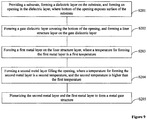
- Figure 9 illustrates an exemplary fabrication process to form a semiconductor structure consistent with the disclosed embodiments; and Figures 3-8 illustrate cross-sectional views of semiconductor structures corresponding to certain stages of the exemplary fabrication process.
- a fabrication process to form a metal gate structure is described as an example.
- the disclosed embodiments can also be configured to form a metal plug, metal interconnect lines, and other semiconductor structures.
- a substrate with certain structures may be provided (S201).
- Figure 3 illustrates a corresponding semiconductor structure.
- a substrate 100 may be provided, a dielectric layer 200 may be formed on the substrate 100, and an opening 300 may be formed in the dielectric layer 200. Bottom of the opening 300 may expose the surface of the substrate 100.
- the substrate 100 may be configured as a platform for subsequent fabrication processes.
- the substrate 100 may include monocrystalline silicon, polycrystalline silicon, amorphous silicon.
- the substrate 100 may also include silicon (Si), germanium (Ge), germanium-silicon alloy (GeSi), or gallium arsenide (GaAs) and other compounds.
- the substrate 100 may include other semiconductor materials.
- the substrate 100 may include a silicon material having an epitaxial layer or on an epitaxial layer.
- a gate structure for forming a planar transistor is described as an example, therefore, the substrate 100 may be a monocrystalline silicon substrate.
- the dielectric layer 200 may be formed to provide electrical isolation between different semiconductor devices, and may also be configured to define the shape and dimensions of subsequently formed gate.
- the opening 300 may be formed in the dielectric layer 200.
- a metal gate structure may be subsequently formed by filling the opening 300 with metal material.
- the dielectric layer 200 may be made of silicon oxide.
- Forming the dielectric layer 200 may include: forming a dielectric material layer on the substrate 100 by a chemical vapor deposition process, a physical vapor deposition process, an atomic layer deposition process, or other film deposition processes; forming a patterned layer on the dielectric material layer; and using the patterned layer as a mask to etch the dielectric material layer until the surface of the substrate 100 is exposed to form the opening 300.
- the patterned layer may be a patterned photoresist layer, and may be formed by coating and photo-lithography processes.
- the patterned layer may be formed by a multiple patterned mask process.
- the multiple patterned mask process may include a self-aligned double patterned (SaDP) process, a self-aligned triple patterned (SaTP) process, or a self-aligned double double patterned (SaDDP) process, etc.
- the opening 300 may be formed by etching the dielectric layer 200. In certain other embodiments, the opening may also be formed by removing the dummy gate formed in the dielectric layer, and other processes may also be used.
- a gate sidewall spacer may be formed on the side wall of the opening 300 (not labeled).
- the gate sidewall spacer may be made of nitride, or oxide, etc.
- the gate sidewall spacer may be made of silicon nitride.
- forming the gate sidewall spacer may include: forming a sidewall spacer material layer covering the top surface of the dielectric layer 200 and the bottom and side surfaces of the opening 300 by a chemical vapor deposition process, a physical vapor deposition process, an atomic layer deposition process, or other film deposition processes; and then performing an anisotropic dry etching process to remove the sidewall spacer material layer on the top surface of the dielectric layer 200 and the bottom of the opening 300 until the top surface of the dielectric layer 200 and the bottom of the opening 300 are exposed.
- the sidewall spacer material layer on the side surface of the opening 300 may be retained to form the gate sidewall spacer.
- a gate dielectric layer and a liner structure layer may be formed (S202).
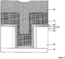
- Figure 4 illustrates a corresponding semiconductor structure.
- a gate dielectric layer 410 may be formed.
- the gate dielectric layer 410 may cover the bottom and side surfaces of the opening 300.
- the gate dielectric layer 410 may be made of oxide, or high-K materials, such as silicon oxide, hafnium oxide, zirconium oxide, hafnium silicon oxide, lanthanum oxide, silica, zirconium oxide, titanium oxide, tantalum oxide, barium strontium titanium, barium titanium oxide, strontium titanium oxide, or alumina oxide, etc.
- the fabrication process may also include forming a liner structure layer 400 on the gate dielectric layer 410.
- the liner structure layer 400 may include a barrier layer 420, a work function layer 430, and an adhesive layer 440. Other layers may also be included.
- the liner structure layer 400 may be sequentially formed on the gate dielectric layer 410 by a chemical vapor deposition process, a physical vapor deposition process, an atomic layer deposition process, or other film deposition processes.
- the barrier layer 420 may be configured to prevent diffusion of metal ions in subsequently formed film structure and the metal gate structure, which impacts the insulating property of the gate dielectric layer 410 and the performance of the channel in the substrate 100. In addition, the barrier layer 420 may be configured to stop etching during the subsequent planarization process.
- the barrier layer 420 may be made of titanium nitride, or tantalum nitride, etc. Specifically, the barrier layer 420 may be formed on the gate dielectric layer 410 over the top surface of the dielectric layer 200 and the bottom and side surfaces of the opening 300 by a chemical vapor deposition process, a physical vapor deposition process, or an atomic layer deposition process, etc. In one embodiment, the barrier layer 420 may include a tantalum nitride layer.
- the work function layer 430 may be configured to adjust the work function of the formed gate structure, and to adjust threshold voltage of the formed semiconductor device.
- the gate structure may be made of a PMOS device. Therefore, the work function layer 430 may include a titanium aluminum layer, an aluminum nitride layer, and a titanium layer. By adjusting the thicknesses of the titanium aluminum layer, the aluminum nitride layer, and the titanium layer, the function of adjusting the work function of the formed gate structure may be achieved.
- the adhesive layer 440 may be configured to improve the connection strength between the metal material and the liner structure layer 400.
- the material of the adhesive layer 440 may be the same as the material of the subsequently formed first metal layer.
- the adhesive layer 440 may include an aluminum seed layer formed by a chemical vapor deposition process, and an aluminum layer formed by a physical vapor deposition process.
- a first metal layer may be formed (S203).
- Figure 5 illustrates a corresponding semiconductor structure.
- a first metal layer 510 may be formed on the liner structure layer 400 over the top surface of the dielectric layer 200.
- the liner structure layer 400 may be omitted, and the first metal layer 510 may be formed on the top surface of the dielectric layer 200.
- other intermediate layer(s) may also be formed between the first metal layer 510 and the dielectric layer 200.
- the first metal layer 510 may cover the top surface of the liner structure layer 400, and protect the liner structure layer 400 from damages caused by the subsequent planarization process.
- the first metal layer 510 may be made of aluminum and formed by a physical vapor deposition process.
- the temperature for forming the first metal layer 510 may be the first temperature.
- the first temperature may be in a range of approximately 300-350 °C. Compared to the temperature for forming aluminum gate by the existing techniques, the first temperature is lower. Therefore, the first metal layer 510 may have more compact structure, smaller grains, and stronger strength.
- the thickness of the first metal layer 510 may be above 300 ⁇ .
- the first metal layer 510 may have more complete crystal structure and fewer defects.
- the first metal layer 510 may also cover the liner structure layer 400 over the bottom of the opening 300 to improve the performance of interface between subsequently formed second metal layer and the liner structure layer 400, and to improve the lattice mismatch issue. Similar to the existing techniques, the first metal layer 510 may also cover the liner structure layer 400 over the side surface of the opening 300 (not labeled).
- a second metal layer may be formed (S204).
- Figure 6 illustrates a corresponding semiconductor structure.
- a second metal layer 520 may be formed.
- the second metal layer 520 may be configured to fill the opening 300 (shown in Figure 5 ) to form a metal gate structure.
- the metal gate structure may be an aluminum gate. Therefore, both the second metal layer 520 and the first metal layer 510 may be made of the same material, aluminum.
- the second metal layer 520 may be formed in the opening 300 by a physical vapor deposition process.
- the first metal layer 510 may also cover the liner structure layer 400 over the bottom of the opening 300 (shown in Figure 5 ). Therefore, the formed metal gate structure may include the first metal layer 510 and the second metal layer 520 filling the opening 300.
- the temperature for forming the second metal layer 520 may be the second temperature.
- the second temperature may be higher than the first temperature. Therefore, compared to the first metal layer 510 formed at the first temperature, the second metal layer 520 may have a higher conductivity and better electrical performance, and may improve the electrical performance of the formed metal gate structure.
- the second temperature may be in a range of approximately 400-450 °C.
- the second metal layer 520 may be made of aluminum, and the second temperature may be approximately 430 °C.
- the second metal layer 520 may be formed on the first metal layer 510.
- the first metal layer 510 may have lower formation temperature and fewer structural defects. Compared to the metal gate structure directly formed at a high temperature in the existing techniques, the second metal layer 520 may have smaller grains and greater hardness.
- the thickness of the second metal layer 520 may be in a range of approximately 2000-5000 ⁇ .
- the second metal layer 520 may also be formed over the dielectric layer 200.
- the second metal layer 520 may also cover part of the first metal layer 510 over the dielectric layer 200.
- a metal gate structure may be formed by planarizing the second metal layer and the first metal layer (S205).
- Figures 7-8 illustrate corresponding semiconductor structures.
- a metal gate structure may be formed by planarizing the second metal layer and the first metal layer until the top surface of the dielectric layer 200 is exposed.
- the planarization process may include performing a first planarization process to remove the second metal layer 520 formed over the dielectric layer 200 (shown in Figure 6 ).
- a chemical mechanical polishing process may be performed to remove the second metal layer 520 formed over the dielectric layer 200.
- the applied pressure may be greater than 1.5 Pa, and the hardness of the polishing pad may be in a range of approximately 80-100 MPa.
- the second metal layer 520 may have even smaller grains and even greater hardness. Therefore, during the first planarization process, amount of the formed fragments may be small, which may effectively reduce the possibility of scratching the wafer surface, reduce scratches on the wafer surface, and improve the flatness of the wafer surface after the planarization process.
- part of thickness of the first metal layer 510 over the dielectric layer 200 may also be removed, such that the thickness of the first metal layer 510 over the dielectric layer 200 may reach a preset thickness.
- the preset thickness is too small, the remaining first metal layer 510A may be difficult to protect the liner structure layer 400. If the preset thickness is too large, it may impact increasing the speed of the planarization process. Specifically, the preset distance may be in a range of approximately 300-1000 ⁇ . Therefore, in one embodiment, during the first planarization process, the total thickness of removing the first metal layer 510 and the second metal layer 520 may be above 3000 ⁇ .
- the planarization process may also include performing a second planarization process to remove the first metal layer 510 or the remaining first metal layer 510A over the dielectric layer 200 until the top surface of the liner structure layer 400 is exposed.
- the second planarization process may be performed by a chemical mechanical polishing process.
- the chemical mechanical polishing process may stop when the top surface of the liner structure layer 400 is exposed.
- the applied pressure may be in a range of approximately 1-2 Pa, and the hardness of the polishing pad may be in a range of approximately 20-40 MPa.
- the first metal layer 510 may have complete crystal structure, small grains and great hardness. Therefore, during the second planarization process, amount of the formed fragments may be small, which may effectively reduce scratches formed on the wafer surface, and improve the flatness of the wafer surface after the planarization process.
- polishing liquid may be added.
- the polishing liquid may have an etching effect to improve the efficiency of the chemical mechanical polishing process. Therefore, the liner structure layer 400 may be configured to stop etching during the chemical mechanical polishing process, and to effectively protect the dielectric layer from effects of the second planarization process.
- the planarization process may include performing a third planarization process until the top surface of the remaining second metal layer 520 and the top surface of the dielectric layer 200 are flush.
- the third planarization process may be performed by a chemical mechanical polishing process.
- the applied pressure may be in a range of approximately 1-2 Pa, and the hardness of the polishing pad may be in a range of approximately 20-40 MPa. Therefore, during the third planarization process, a polishing grinding process may be performed onto the wafer surface to improve the flatness of the wafer surface.
- the second metal layer 520 in the opening may have complete crystal structure, small grains and great hardness.
- amount of the formed fragments may be small, which may effectively reduce scratches formed on the wafer surface, and improve the flatness of the wafer surface after the planarization process.
- the chemical mechanical polishing process may stop when the top surface of the dielectric layer 200 is exposed. Or the chemical mechanical polishing process may remove part of thickness of the dielectric layer 200 and the second metal layer 520, to ensure the liner structure layer 400 and the gate dielectric layer 410 formed on the dielectric layer 200 are thoroughly removed.
- the metal layer may be formed by a film deposition process at one time.
- the reflectivity of the wafer surface may be 51.3 %, and the roughness of the wafer surface may be 10.1%.
- the disclosed embodiments by forming the first metal layer at a low temperature before forming the second metal layer at a high temperature, after forming the metal gate structure by the planarization process, the reflectivity of the wafer surface may be 81.9%, and the roughness of the wafer surface may be 1.64%. Therefore, the disclosed embodiments may effectively improve the flatness of the wafer surface after the planarization process, improve the accuracy of the process, and improve manufacturing yield of the devices.
- the first metal layer may be formed over the dielectric layer and the bottom of the opening.
- the second metal layer may be formed, filling the opening.
- the first metal layer may be formed at the first temperature
- the second metal layer may be formed at the second temperature.
- the second temperature may be higher than the first temperature. Therefore, the first metal layer may have complete crystal structure, small grains and great hardness. Because of the buffering effect of the first metal layer, the second metal layer may have even smaller grains and even greater hardness. Therefore, during the polishing process, amount of the formed fragments may be small, which may effectively reduce the possibility of scratching the wafer surface, to improve the flatness of the wafer surface after the planarization process.
Landscapes
- Internal Circuitry In Semiconductor Integrated Circuit Devices (AREA)
- Chemical & Material Sciences (AREA)
- Composite Materials (AREA)
- Engineering & Computer Science (AREA)
- Materials Engineering (AREA)
- Insulated Gate Type Field-Effect Transistor (AREA)
Abstract
Description
- This application claims the priority of Chinese patent application No.
201610213621.7, filed on April 7, 2016 - The present invention generally relates to the field of semiconductor manufacturing and, more particularly, relates to a semiconductor structure and fabrication techniques thereof.
- With the rapid development of ultra-large-scale integration, the fabrication process of integrated circuits becomes more and more complex and sophisticated. To improve integration degree and to reduce manufacturing cost, the number of semiconductor components per unit area in the chip increases. Planar wiring has been difficult to meet the demand of high-density distribution of semiconductor components. Multi-layer wiring technology is performed to use vertical space of the chip to further improve the integration degree of the devices. However, using the multi-layer wiring technology can cause rough surface of the silicon wafer, which may affect patterning processes. Therefore, to realize the multi-layer wiring structure, each layer of the semiconductor structure first needs to have a high level of flatness; and the semiconductor structures on the wafer also need to be planarized.
- A chemical mechanical polishing (CMP) process is one of the most common planarization processes. The planarization efficiency of the chemical mechanical polishing process is high, and CMP process has become an indispensable semiconductor process technology.
- However, after performing the planarization process onto semiconductor structures formed by existing fabrication techniques, the wafer surface is prone to scratches.
- It is an object of the present invention to provide a semiconductor structure and a method for fabricating the semiconductor structure by which one or more problems set forth above and other problems are solved or at least reduced.
- The object is achieved by the features of the respective independent claims. Further embodiments are defined in the respective dependent claims.
- A first aspect of the present invention includes a method for fabricating a semiconductor structure. The method includes providing a substrate having a dielectric layer formed on the substrate, wherein an opening is formed in the dielectric layer, and bottom of the opening exposes surface of the substrate. The method also includes forming a first metal layer over of the dielectric layer, wherein a temperature for forming the first metal layer is a first temperature. In addition, the method includes forming a second metal layer filling the opening, wherein a temperature for forming the second metal layer is a second temperature, and the second temperature is higher than the first temperature. Further, the method includes planarizing the second metal layer and the first metal layer until the top surface of the dielectric layer is exposed.
- Preferably, the first temperature is in a range of approximately 300-350 °C.
- Preferably, the second temperature is in a range of approximately 400-450 °C.
- Preferably, the first metal layer and the second metal layer are made of a same material. For example, the first metal layer and the second metal layer are made of aluminum.
- Preferably, a physical vapor deposition process is performed to form the first metal layer or the second metal layer.
- Preferably, a thickness of the first metal layer is larger than 300 Å.
- Preferably, a thickness of the second metal layer is in a range of approximately 2000-5000 Å.
- Preferably, the first metal layer is also formed over the bottom of the opening, and the second metal layer is also formed over the dielectric layer.
- Preferably, planarizing the second metal layer and the first metal layer includes: performing a first planarization process to remove the second metal layer formed over the dielectric layer; performing a second planarization process to remove the first metal layer formed over the dielectric layer until the top surface of the liner structure layer is exposed; and performing a third planarization process until the top surface of the remaining second metal layer and the top surface of the dielectric layer are flush.
- Preferably, the first planarization process also includes: removing part of thickness of the first metal layer formed over the dielectric layer, such that the thickness of the first metal layer formed over the dielectric layer reaches a preset thickness. For example, the preset thickness may be in a range of approximately 300-1000 Å.
- Preferably, wherein one or more processes in the first planarization process, the second planarization process and the third planarization process include: a chemical mechanical polishing process.
- Preferably, during the first planarization process performed by the chemical mechanical polishing process: a pressure is larger than 1.5 Pa; and a hardness of the polishing pad is in a range of approximately 80-100 MPa.
- Preferably, during the second planarization process performed by the chemical mechanical polishing process: a pressure is in a range of approximately 1-2 Pa; and a hardness of the polishing pad is in a range of approximately 20-40 MPa.
- Preferably, during the third planarization process performed by the chemical mechanical polishing process: a pressure is in a range of approximately 1-2 Pa; and a hardness of the polishing pad is in a range of approximately 20-40 MPa.
- Preferably, after providing the substrate and before forming the first metal layer, further including: forming a liner structure layer over the bottom and side surfaces of the opening.
- Preferably, along a direction away from the substrate, the liner structure layer sequentially includes: a barrier layer; a work function layer; and an adhesive layer.
- Preferably, the barrier layer includes a tantalum nitride layer.
- Preferably, the work function layer includes a titanium aluminum layer, an aluminum nitride layer, and a titanium layer sequentially formed on the barrier layer.
- Preferably, the adhesive layer is made of the same material as the first metal layer.
- Preferably, after providing the substrate and before forming the first metal layer, further including: the semiconductor structure is a metal gate structure; and forming a gate dielectric layer covering the bottom of the opening.
- Other aspects of the present invention can be understood by those skilled in the art in light of the description, the claims, and the drawings of the present invention.
-
-
Figures 1-2 illustrate cross-sectional views of semiconductor structures corresponding to certain stages of an existing fabrication process of a semiconductor structure; -
Figures 3-8 illustrate cross-sectional views of semiconductor structures corresponding to certain stages of a fabrication process of a semiconductor structure consistent with the disclosed embodiments; and -
Figure 9 illustrates an exemplary fabrication process to form a semiconductor structure consistent with the disclosed embodiments. - Reference will now be made in detail to exemplary embodiments of the invention, which are illustrated in the accompanying drawings. Wherever possible, the same reference numbers will be used throughout the drawings to refer to the same or the alike parts.
-
Figures 1-2 illustrate cross-sectional views of semiconductor structures corresponding to certain stages of an existing fabrication process of a semiconductor structure. A fabrication process to form a metal gate structure is described as an example. - As shown in
Figure 1 , the fabrication process includes providing asubstrate 10, forming adielectric layer 20 on thesubstrate 10, and forming an opening in thedielectric layer 20. The fabrication process also includes forming aliner material layer 30, where theliner material layer 30 covers the bottom and side surfaces of the opening and the top surface of thedielectric layer 20; and forming ametal layer 40, where themetal layer 40 fills the opening and covers theliner material layer 30 formed on the top surface of thedielectric layer 20. - As shown in
Figure 2 , further, the existing fabrication process includes forming ametal gate 40g and aliner layer 30r by planarizing themetal layer 40 to remove themetal layer 40 and theliner material layer 30 formed on the top surface of thedielectric layer 20. The top surfaces of themetal gate 40g, theliner layer 30r and thedielectric layer 20 are flush. - In the existing techniques, the
metal layer 40 is formed by a film deposition process at one time, and temperature in the process of forming themetal layer 40 is high. When themetal layer 40 is made of aluminum, the temperature of forming themetal layer 40 is approximately 430 °C. Therefore, the density of the formedmetal layer 40 is small. That is, themetal layer 40 is not compact enough, thus the strength of themetal layer 40 is small. During forming themetal gate 40g, it is easy to form metal fragments or particles. During the planarization process, the metal fragments or particles tend to scratch the wafer surface, thus resulting in scratches on the wafer surface, and impacting improving the flatness of the wafer surface. - The present invention provides an improved semiconductor structure and fabrication process.
Figure 9 illustrates an exemplary fabrication process to form a semiconductor structure consistent with the disclosed embodiments; andFigures 3-8 illustrate cross-sectional views of semiconductor structures corresponding to certain stages of the exemplary fabrication process. In one embodiment, a fabrication process to form a metal gate structure is described as an example. In certain other embodiments, the disclosed embodiments can also be configured to form a metal plug, metal interconnect lines, and other semiconductor structures. - As shown in
Figure 9 , at the beginning of the fabrication process, a substrate with certain structures may be provided (S201).Figure 3 illustrates a corresponding semiconductor structure. - Referring to
Figure 3 , asubstrate 100 may be provided, adielectric layer 200 may be formed on thesubstrate 100, and anopening 300 may be formed in thedielectric layer 200. Bottom of theopening 300 may expose the surface of thesubstrate 100. - The
substrate 100 may be configured as a platform for subsequent fabrication processes. Thesubstrate 100 may include monocrystalline silicon, polycrystalline silicon, amorphous silicon. Thesubstrate 100 may also include silicon (Si), germanium (Ge), germanium-silicon alloy (GeSi), or gallium arsenide (GaAs) and other compounds. In addition, thesubstrate 100 may include other semiconductor materials. Further, thesubstrate 100 may include a silicon material having an epitaxial layer or on an epitaxial layer. In one embodiment, a gate structure for forming a planar transistor is described as an example, therefore, thesubstrate 100 may be a monocrystalline silicon substrate. - The
dielectric layer 200 may be formed to provide electrical isolation between different semiconductor devices, and may also be configured to define the shape and dimensions of subsequently formed gate. Theopening 300 may be formed in thedielectric layer 200. A metal gate structure may be subsequently formed by filling theopening 300 with metal material. Specifically, in one embodiment, thedielectric layer 200 may be made of silicon oxide. - Forming the
dielectric layer 200 may include: forming a dielectric material layer on thesubstrate 100 by a chemical vapor deposition process, a physical vapor deposition process, an atomic layer deposition process, or other film deposition processes; forming a patterned layer on the dielectric material layer; and using the patterned layer as a mask to etch the dielectric material layer until the surface of thesubstrate 100 is exposed to form theopening 300. - The patterned layer may be a patterned photoresist layer, and may be formed by coating and photo-lithography processes. In addition, to decrease the dimensions of the subsequently formed metal gate structure, and to decrease the dimensions of the semiconductor device, the patterned layer may be formed by a multiple patterned mask process. The multiple patterned mask process may include a self-aligned double patterned (SaDP) process, a self-aligned triple patterned (SaTP) process, or a self-aligned double double patterned (SaDDP) process, etc.
- In one embodiment, the
opening 300 may be formed by etching thedielectric layer 200. In certain other embodiments, the opening may also be formed by removing the dummy gate formed in the dielectric layer, and other processes may also be used. - To prevent damages to the formed channel region of the semiconductor device caused by the subsequent semiconductor processes, and to reduce occurrence of source-drain punch-through phenomenon, a gate sidewall spacer may be formed on the side wall of the opening 300 (not labeled). The gate sidewall spacer may be made of nitride, or oxide, etc. In one embodiment, the gate sidewall spacer may be made of silicon nitride.
- Specifically, forming the gate sidewall spacer may include: forming a sidewall spacer material layer covering the top surface of the
dielectric layer 200 and the bottom and side surfaces of theopening 300 by a chemical vapor deposition process, a physical vapor deposition process, an atomic layer deposition process, or other film deposition processes; and then performing an anisotropic dry etching process to remove the sidewall spacer material layer on the top surface of thedielectric layer 200 and the bottom of theopening 300 until the top surface of thedielectric layer 200 and the bottom of theopening 300 are exposed. The sidewall spacer material layer on the side surface of theopening 300 may be retained to form the gate sidewall spacer. - Returning to
Figure 9 , after providing the substrate having certain structures, a gate dielectric layer and a liner structure layer may be formed (S202).Figure 4 illustrates a corresponding semiconductor structure. - As shown in
Figure 4 , agate dielectric layer 410 may be formed. Thegate dielectric layer 410 may cover the bottom and side surfaces of theopening 300. - The
gate dielectric layer 410 may be made of oxide, or high-K materials, such as silicon oxide, hafnium oxide, zirconium oxide, hafnium silicon oxide, lanthanum oxide, silica, zirconium oxide, titanium oxide, tantalum oxide, barium strontium titanium, barium titanium oxide, strontium titanium oxide, or alumina oxide, etc. - After forming the
gate dielectric layer 410 and before forming a first metal layer over thegate dielectric layer 410, the fabrication process may also include forming aliner structure layer 400 on thegate dielectric layer 410. - Along a direction away from the
substrate 100, theliner structure layer 400 may include abarrier layer 420, awork function layer 430, and anadhesive layer 440. Other layers may also be included. - Specifically, the
liner structure layer 400 may be sequentially formed on thegate dielectric layer 410 by a chemical vapor deposition process, a physical vapor deposition process, an atomic layer deposition process, or other film deposition processes. - The
barrier layer 420 may be configured to prevent diffusion of metal ions in subsequently formed film structure and the metal gate structure, which impacts the insulating property of thegate dielectric layer 410 and the performance of the channel in thesubstrate 100. In addition, thebarrier layer 420 may be configured to stop etching during the subsequent planarization process. Thebarrier layer 420 may be made of titanium nitride, or tantalum nitride, etc. Specifically, thebarrier layer 420 may be formed on thegate dielectric layer 410 over the top surface of thedielectric layer 200 and the bottom and side surfaces of theopening 300 by a chemical vapor deposition process, a physical vapor deposition process, or an atomic layer deposition process, etc. In one embodiment, thebarrier layer 420 may include a tantalum nitride layer. - The
work function layer 430 may be configured to adjust the work function of the formed gate structure, and to adjust threshold voltage of the formed semiconductor device. Specifically, in one embodiment, the gate structure may be made of a PMOS device. Therefore, thework function layer 430 may include a titanium aluminum layer, an aluminum nitride layer, and a titanium layer. By adjusting the thicknesses of the titanium aluminum layer, the aluminum nitride layer, and the titanium layer, the function of adjusting the work function of the formed gate structure may be achieved. - The
adhesive layer 440 may be configured to improve the connection strength between the metal material and theliner structure layer 400. Specifically, the material of theadhesive layer 440 may be the same as the material of the subsequently formed first metal layer. In one embodiment, theadhesive layer 440 may include an aluminum seed layer formed by a chemical vapor deposition process, and an aluminum layer formed by a physical vapor deposition process. - Returning to
Figure 9 , after forming the gate dielectric layer and the liner structure layer, a first metal layer may be formed (S203).Figure 5 illustrates a corresponding semiconductor structure. - As shown in
Figure 5 , afirst metal layer 510 may be formed on theliner structure layer 400 over the top surface of thedielectric layer 200. In certain embodiments, theliner structure layer 400 may be omitted, and thefirst metal layer 510 may be formed on the top surface of thedielectric layer 200. In certain other embodiments, other intermediate layer(s) may also be formed between thefirst metal layer 510 and thedielectric layer 200. - The
first metal layer 510 may cover the top surface of theliner structure layer 400, and protect theliner structure layer 400 from damages caused by the subsequent planarization process. Specifically, in one embodiment, thefirst metal layer 510 may be made of aluminum and formed by a physical vapor deposition process. - The temperature for forming the
first metal layer 510 may be the first temperature. Specifically, the first temperature may be in a range of approximately 300-350 °C. Compared to the temperature for forming aluminum gate by the existing techniques, the first temperature is lower. Therefore, thefirst metal layer 510 may have more compact structure, smaller grains, and stronger strength. - If the thickness of the
first metal layer 510 is too small, it is difficult to protect theliner structure layer 400 during the subsequent planarization process. Therefore, in one embodiment, the thickness of thefirst metal layer 510 may be above 300 Å. - In addition, because the temperature for forming the
first metal layer 510 is low, thefirst metal layer 510 may have more complete crystal structure and fewer defects. In one embodiment, thefirst metal layer 510 may also cover theliner structure layer 400 over the bottom of theopening 300 to improve the performance of interface between subsequently formed second metal layer and theliner structure layer 400, and to improve the lattice mismatch issue. Similar to the existing techniques, thefirst metal layer 510 may also cover theliner structure layer 400 over the side surface of the opening 300 (not labeled). - Returning to
Figure 9 , after forming the first metal layer, a second metal layer may be formed (S204).Figure 6 illustrates a corresponding semiconductor structure. - As shown in
Figure 6 , asecond metal layer 520 may be formed. Thesecond metal layer 520 may be configured to fill the opening 300 (shown inFigure 5 ) to form a metal gate structure. Specifically, in one embodiment, the metal gate structure may be an aluminum gate. Therefore, both thesecond metal layer 520 and thefirst metal layer 510 may be made of the same material, aluminum. Thesecond metal layer 520 may be formed in theopening 300 by a physical vapor deposition process. - In one embodiment, the
first metal layer 510 may also cover theliner structure layer 400 over the bottom of the opening 300 (shown inFigure 5 ). Therefore, the formed metal gate structure may include thefirst metal layer 510 and thesecond metal layer 520 filling theopening 300. - The temperature for forming the
second metal layer 520 may be the second temperature. The second temperature may be higher than the first temperature. Therefore, compared to thefirst metal layer 510 formed at the first temperature, thesecond metal layer 520 may have a higher conductivity and better electrical performance, and may improve the electrical performance of the formed metal gate structure. Specifically, the second temperature may be in a range of approximately 400-450 °C. In one embodiment, thesecond metal layer 520 may be made of aluminum, and the second temperature may be approximately 430 °C. - Further, the
second metal layer 520 may be formed on thefirst metal layer 510. Thefirst metal layer 510 may have lower formation temperature and fewer structural defects. Compared to the metal gate structure directly formed at a high temperature in the existing techniques, thesecond metal layer 520 may have smaller grains and greater hardness. - If the thickness of the
second metal layer 520 is too small, it is difficult to sufficiently fill the opening 300 (shown inFigure 5 ), thus impacting the electrical performance of the formed metal gate structure. If the thickness of thesecond metal layer 520 is too large, it is easy to waste materials and to increase the fabrication difficulty. In one embodiment, the thickness of thesecond metal layer 520 may be in a range of approximately 2000-5000 Å. - To ensure the
second metal layer 520 completely fill the opening 300 (shown inFigure 5 ), in one embodiment, thesecond metal layer 520 may also be formed over thedielectric layer 200. In other words, thesecond metal layer 520 may also cover part of thefirst metal layer 510 over thedielectric layer 200. - Returning to
Figure 9 , after forming the second metal layer, a metal gate structure may be formed by planarizing the second metal layer and the first metal layer (S205).Figures 7-8 illustrate corresponding semiconductor structures. - As shown in
Figures 7-8 , a metal gate structure may be formed by planarizing the second metal layer and the first metal layer until the top surface of thedielectric layer 200 is exposed. - As shown in
Figure 7 , the planarization process may include performing a first planarization process to remove thesecond metal layer 520 formed over the dielectric layer 200 (shown inFigure 6 ). - Specifically, a chemical mechanical polishing process may be performed to remove the
second metal layer 520 formed over thedielectric layer 200. To improve the efficiency of the planarization process and to shorten the time of forming the metal gate structure, in one embodiment, during performing the first planarization process by the chemical mechanical polishing process, the applied pressure may be greater than 1.5 Pa, and the hardness of the polishing pad may be in a range of approximately 80-100 MPa. - Because of the buffering effect of the
first metal layer 510, thesecond metal layer 520 may have even smaller grains and even greater hardness. Therefore, during the first planarization process, amount of the formed fragments may be small, which may effectively reduce the possibility of scratching the wafer surface, reduce scratches on the wafer surface, and improve the flatness of the wafer surface after the planarization process. - In one embodiment, to improve the speed of the planarization process, during performing the first planarization process, part of thickness of the
first metal layer 510 over thedielectric layer 200 may also be removed, such that the thickness of thefirst metal layer 510 over thedielectric layer 200 may reach a preset thickness. - If the preset thickness is too small, the remaining
first metal layer 510A may be difficult to protect theliner structure layer 400. If the preset thickness is too large, it may impact increasing the speed of the planarization process. Specifically, the preset distance may be in a range of approximately 300-1000 Å. Therefore, in one embodiment, during the first planarization process, the total thickness of removing thefirst metal layer 510 and thesecond metal layer 520 may be above 3000 Å. - As shown in
Figure 8 , the planarization process may also include performing a second planarization process to remove thefirst metal layer 510 or the remainingfirst metal layer 510A over thedielectric layer 200 until the top surface of theliner structure layer 400 is exposed. - Specifically, the second planarization process may be performed by a chemical mechanical polishing process. The chemical mechanical polishing process may stop when the top surface of the
liner structure layer 400 is exposed. In one embodiment, during performing the second planarization process by the chemical mechanical polishing process, the applied pressure may be in a range of approximately 1-2 Pa, and the hardness of the polishing pad may be in a range of approximately 20-40 MPa. - Because the temperature for forming the
first metal layer 510 is low, thefirst metal layer 510 may have complete crystal structure, small grains and great hardness. Therefore, during the second planarization process, amount of the formed fragments may be small, which may effectively reduce scratches formed on the wafer surface, and improve the flatness of the wafer surface after the planarization process. - During the chemical mechanical polishing process, polishing liquid may be added. The polishing liquid may have an etching effect to improve the efficiency of the chemical mechanical polishing process. Therefore, the
liner structure layer 400 may be configured to stop etching during the chemical mechanical polishing process, and to effectively protect the dielectric layer from effects of the second planarization process. - Further, as shown in
Figure 8 , the planarization process may include performing a third planarization process until the top surface of the remainingsecond metal layer 520 and the top surface of thedielectric layer 200 are flush. - Specifically, the third planarization process may be performed by a chemical mechanical polishing process. In one embodiment, during performing the third planarization process by the chemical mechanical polishing process, the applied pressure may be in a range of approximately 1-2 Pa, and the hardness of the polishing pad may be in a range of approximately 20-40 MPa. Therefore, during the third planarization process, a polishing grinding process may be performed onto the wafer surface to improve the flatness of the wafer surface.
- Since the
first metal layer 510 may be formed over the bottom of the opening, thesecond metal layer 520 in the opening may have complete crystal structure, small grains and great hardness. During the third planarization process, amount of the formed fragments may be small, which may effectively reduce scratches formed on the wafer surface, and improve the flatness of the wafer surface after the planarization process. - The chemical mechanical polishing process may stop when the top surface of the
dielectric layer 200 is exposed. Or the chemical mechanical polishing process may remove part of thickness of thedielectric layer 200 and thesecond metal layer 520, to ensure theliner structure layer 400 and thegate dielectric layer 410 formed on thedielectric layer 200 are thoroughly removed. - Specifically, in the existing techniques, the metal layer may be formed by a film deposition process at one time. After the planarization process, the reflectivity of the wafer surface may be 51.3 %, and the roughness of the wafer surface may be 10.1%. In the disclosed embodiments, by forming the first metal layer at a low temperature before forming the second metal layer at a high temperature, after forming the metal gate structure by the planarization process, the reflectivity of the wafer surface may be 81.9%, and the roughness of the wafer surface may be 1.64%. Therefore, the disclosed embodiments may effectively improve the flatness of the wafer surface after the planarization process, improve the accuracy of the process, and improve manufacturing yield of the devices.
- Accordingly, the first metal layer may be formed over the dielectric layer and the bottom of the opening. The second metal layer may be formed, filling the opening. The first metal layer may be formed at the first temperature, and the second metal layer may be formed at the second temperature. The second temperature may be higher than the first temperature. Therefore, the first metal layer may have complete crystal structure, small grains and great hardness. Because of the buffering effect of the first metal layer, the second metal layer may have even smaller grains and even greater hardness. Therefore, during the polishing process, amount of the formed fragments may be small, which may effectively reduce the possibility of scratching the wafer surface, to improve the flatness of the wafer surface after the planarization process.
Claims (15)
- A method for fabricating a semiconductor structure, comprising:providing a substrate having a dielectric layer formed on the substrate, wherein an opening is formed in the dielectric layer, and bottom of the opening exposes surface of the substrate;forming a first metal layer over the top of the dielectric layer, wherein a temperature for forming the first metal layer is a first temperature;forming a second metal layer filling the opening, wherein a temperature for forming the second metal layer is a second temperature, and the second temperature is higher than the first temperature; andplanarizing the second metal layer and the first metal layer until the top surface of the dielectric layer is exposed.
- The method according to claim 1, wherein:the first temperature is in a range of approximately 300-350 °C; and/orthe second temperature is in a range of approximately 400-450 °C.
- The method according to claim 1 or 2, wherein:the first metal layer and the second metal layer are made of a same material; and/orthe first metal layer and the second metal layer are made of aluminum.
- The method according to any one of the claims 1-3, wherein:a physical vapor deposition process is performed to form the first metal layer or the second metal layer.
- The method according to any one of the claims 1-4, wherein:a thickness of the first metal layer is larger than 300 Å; and/or a thickness of the second metal layer is in a range of approximately 2000-5000 Å.
- The method according to any one of the claims 1-5, wherein:the first metal layer is also formed over the bottom of the opening; andthe second metal layer is also formed over the dielectric layer.
- The method according to any one of the claims 1-6, wherein a planarization process includes:performing a first planarization process to remove the second metal layer formed over the dielectric layer;performing a second planarization process to remove the first metal layer formed over the dielectric layer until the top surface of the liner structure layer is exposed; andperforming a third planarization process until the top surface of the remaining second metal layer and the top surface of the dielectric layer are flush.
- The method according to claim 7, wherein the first planarization process also includes:removing part of thickness of the first metal layer formed over the dielectric layer, such that the thickness of the first metal layer formed over the dielectric layer reaches a preset thickness;wherein preferably: the preset thickness is in a range of approximately 300-1000 Å.
- The method according to claim 7 or 8, wherein one or more processes in the first planarization process, the second planarization process and the third planarization process include: a chemical mechanical polishing process.
- The method according to any one of the claims 7-9, wherein, during the first planarization process performed by the chemical mechanical polishing process:a pressure is larger than 1.5 Pa; anda hardness of the polishing pad is in a range of approximately 80-100 MPa.
- The method according to any one of the claims 7-10, wherein, during the second planarization process performed by the chemical mechanical polishing process:a pressure is in a range of approximately 1-2 Pa; anda hardness of the polishing pad is in a range of approximately 20-40 MPa.
- The method according to any one of the claims 7-11, wherein, during the third planarization process performed by the chemical mechanical polishing process:a pressure is in a range of approximately 1-2 Pa; anda hardness of the polishing pad is in a range of approximately 20-40 MPa.
- The method according to any one of the claims 1-12, after providing the substrate and before forming the first metal layer, further including:forming a liner structure layer over the bottom and side surfaces of the opening.
- The method according to claim 13, wherein, along a direction away from the substrate, the liner structure layer sequentially includes:a barrier layer, wherein preferably the barrier layer includes a tantalum nitride layer;a work function layer, wherein preferably the work function layer includes a titanium aluminum layer, an aluminum nitride layer, and a titanium layer sequentially formed on the barrier layer; andan adhesive layer, wherein preferably the adhesive layer is made of the same material as the first metal layer.
- The method according to any one of the claims 1-14, after providing the substrate and before forming the first metal layer, further including:the semiconductor structure is a metal gate structure; andforming a gate dielectric layer covering the bottom of the opening.
Applications Claiming Priority (1)
| Application Number | Priority Date | Filing Date | Title |
|---|---|---|---|
| CN201610213621.7A CN107275278A (en) | 2016-04-07 | 2016-04-07 | The forming method of semiconductor structure |
Publications (2)
| Publication Number | Publication Date |
|---|---|
| EP3240021A1 true EP3240021A1 (en) | 2017-11-01 |
| EP3240021B1 EP3240021B1 (en) | 2020-09-23 |
Family
ID=58464299
Family Applications (1)
| Application Number | Title | Priority Date | Filing Date |
|---|---|---|---|
| EP17163839.8A Not-in-force EP3240021B1 (en) | 2016-04-07 | 2017-03-30 | A method for fabricating a semiconductor structure |
Country Status (3)
| Country | Link |
|---|---|
| US (1) | US10062572B2 (en) |
| EP (1) | EP3240021B1 (en) |
| CN (1) | CN107275278A (en) |
Families Citing this family (3)
| Publication number | Priority date | Publication date | Assignee | Title |
|---|---|---|---|---|
| CN108573871B (en) * | 2017-03-07 | 2021-06-08 | 中芯国际集成电路制造(上海)有限公司 | Semiconductor device and method of forming the same |
| US10490649B2 (en) * | 2017-05-30 | 2019-11-26 | Taiwan Semiconductor Manufacturing Company, Ltd. | Method of fabricating semiconductor device with adhesion layer |
| CN109427685B (en) * | 2017-08-24 | 2020-11-10 | 联华电子股份有限公司 | Buried character line of dynamic random access memory and method of making the same |
Citations (8)
| Publication number | Priority date | Publication date | Assignee | Title |
|---|---|---|---|---|
| US5200030A (en) * | 1990-10-25 | 1993-04-06 | Hyundai Electronics Industries Co., Ltd. | Method for manufacturing a planarized metal layer for semiconductor device |
| EP0799903A2 (en) * | 1996-04-05 | 1997-10-08 | Applied Materials, Inc. | Methods of sputtering a metal onto a substrate and semiconductor processing apparatus |
| US6287963B1 (en) * | 1990-11-05 | 2001-09-11 | Stmicroelectronics, Inc. | Method for forming a metal contact |
| US20030186539A1 (en) * | 2002-03-12 | 2003-10-02 | Jong-Myeong Lee | Methods for forming metal interconnections for semiconductor devices having multiple metal depositions |
| JP2005116592A (en) * | 2003-10-03 | 2005-04-28 | Takehide Shirato | Field effect transistor |
| US20120326243A1 (en) * | 2011-06-22 | 2012-12-27 | Hsin-Fu Huang | Transistor having aluminum metal gate and method of making the same |
| US20130037865A1 (en) * | 2011-08-10 | 2013-02-14 | International Business Machines Corporation | Semiconductor structure having a wetting layer |
| US20130302974A1 (en) * | 2012-05-08 | 2013-11-14 | Globalfoundries Inc. | Replacement gate electrode fill at reduced temperatures |
Family Cites Families (5)
| Publication number | Priority date | Publication date | Assignee | Title |
|---|---|---|---|---|
| US6881664B2 (en) * | 2001-08-28 | 2005-04-19 | Lsi Logic Corporation | Process for planarizing upper surface of damascene wiring structure for integrated circuit structures |
| US20090229667A1 (en) * | 2008-03-14 | 2009-09-17 | Solarmer Energy, Inc. | Translucent solar cell |
| CN102554748B (en) * | 2010-12-23 | 2014-11-05 | 中芯国际集成电路制造(北京)有限公司 | Polishing method |
| US8432002B2 (en) * | 2011-06-28 | 2013-04-30 | International Business Machines Corporation | Method and structure for low resistive source and drain regions in a replacement metal gate process flow |
| US8772159B2 (en) * | 2012-02-01 | 2014-07-08 | United Microelectronics Corp. | Method of fabricating electrical contact |
-
2016
- 2016-04-07 CN CN201610213621.7A patent/CN107275278A/en active Pending
-
2017
- 2017-03-30 EP EP17163839.8A patent/EP3240021B1/en not_active Not-in-force
- 2017-03-31 US US15/476,249 patent/US10062572B2/en active Active
Patent Citations (8)
| Publication number | Priority date | Publication date | Assignee | Title |
|---|---|---|---|---|
| US5200030A (en) * | 1990-10-25 | 1993-04-06 | Hyundai Electronics Industries Co., Ltd. | Method for manufacturing a planarized metal layer for semiconductor device |
| US6287963B1 (en) * | 1990-11-05 | 2001-09-11 | Stmicroelectronics, Inc. | Method for forming a metal contact |
| EP0799903A2 (en) * | 1996-04-05 | 1997-10-08 | Applied Materials, Inc. | Methods of sputtering a metal onto a substrate and semiconductor processing apparatus |
| US20030186539A1 (en) * | 2002-03-12 | 2003-10-02 | Jong-Myeong Lee | Methods for forming metal interconnections for semiconductor devices having multiple metal depositions |
| JP2005116592A (en) * | 2003-10-03 | 2005-04-28 | Takehide Shirato | Field effect transistor |
| US20120326243A1 (en) * | 2011-06-22 | 2012-12-27 | Hsin-Fu Huang | Transistor having aluminum metal gate and method of making the same |
| US20130037865A1 (en) * | 2011-08-10 | 2013-02-14 | International Business Machines Corporation | Semiconductor structure having a wetting layer |
| US20130302974A1 (en) * | 2012-05-08 | 2013-11-14 | Globalfoundries Inc. | Replacement gate electrode fill at reduced temperatures |
Also Published As
| Publication number | Publication date |
|---|---|
| CN107275278A (en) | 2017-10-20 |
| EP3240021B1 (en) | 2020-09-23 |
| US10062572B2 (en) | 2018-08-28 |
| US20170294315A1 (en) | 2017-10-12 |
Similar Documents
| Publication | Publication Date | Title |
|---|---|---|
| US10347729B2 (en) | Device for improving performance through gate cut last process | |
| US10050121B2 (en) | Replacement metal gate structures | |
| US9105632B2 (en) | Semiconductor structures | |
| US11877442B2 (en) | Semiconductor memory device | |
| TWI759277B (en) | Semiconductor devices, finfet devices and methods of forming the same | |
| CN102790055B (en) | DRAM structure and its manufacturing method and IC structure and its manufacturing method | |
| US20200066880A1 (en) | Method for manufacturing semiconductor structure with unleveled gate structure | |
| US20150076624A1 (en) | Integrated circuits having smooth metal gates and methods for fabricating same | |
| CN112151380B (en) | Semiconductor structures and methods of forming them | |
| US9384978B1 (en) | Method of forming trenches | |
| US10679902B2 (en) | Semiconductor device and fabrication method thereof | |
| EP3240021B1 (en) | A method for fabricating a semiconductor structure | |
| US8435900B2 (en) | Method for manufacturing a transistor | |
| CN103904028A (en) | Semiconductor structure and manufacturing method thereof | |
| KR101695902B1 (en) | Method of manufacturing a semiconductor device | |
| CN111696864B (en) | Semiconductor devices and methods of forming the same | |
| US8193099B1 (en) | Protecting exposed metal gate structures from etching processes in integrated circuit manufacturing | |
| CN116759305A (en) | Method for manufacturing metal gate | |
| CN108428633A (en) | Semiconductor structure with gate height scaling | |
| CN115602621A (en) | Semiconductor device and manufacturing method thereof | |
| TW202004920A (en) | Semiconductor structure having metal gate and forming method thereof | |
| CN112151451B (en) | Semiconductor structure and method of forming the same | |
| CN114078744B (en) | Semiconductor structure and method for forming the same | |
| CN103794562B (en) | Semiconductor device manufacturing method | |
| CN110277346A (en) | The forming method of semiconductor structure |
Legal Events
| Date | Code | Title | Description |
|---|---|---|---|
| PUAI | Public reference made under article 153(3) epc to a published international application that has entered the european phase |
Free format text: ORIGINAL CODE: 0009012 |
|
| STAA | Information on the status of an ep patent application or granted ep patent |
Free format text: STATUS: THE APPLICATION HAS BEEN PUBLISHED |
|
| AK | Designated contracting states |
Kind code of ref document: A1 Designated state(s): AL AT BE BG CH CY CZ DE DK EE ES FI FR GB GR HR HU IE IS IT LI LT LU LV MC MK MT NL NO PL PT RO RS SE SI SK SM TR |
|
| AX | Request for extension of the european patent |
Extension state: BA ME |
|
| STAA | Information on the status of an ep patent application or granted ep patent |
Free format text: STATUS: REQUEST FOR EXAMINATION WAS MADE |
|
| 17P | Request for examination filed |
Effective date: 20180427 |
|
| RBV | Designated contracting states (corrected) |
Designated state(s): AL AT BE BG CH CY CZ DE DK EE ES FI FR GB GR HR HU IE IS IT LI LT LU LV MC MK MT NL NO PL PT RO RS SE SI SK SM TR |
|
| RAP1 | Party data changed (applicant data changed or rights of an application transferred) |
Owner name: SEMICONDUCTOR MANUFACTURING INTERNATIONAL (SHANGHA Owner name: SEMICONDUCTOR MANUFACTURING INTERNATIONAL (BEIJING |
|
| RIC1 | Information provided on ipc code assigned before grant |
Ipc: H01L 29/49 20060101ALI20200311BHEP Ipc: H01L 21/768 20060101AFI20200311BHEP Ipc: H01L 23/532 20060101ALI20200311BHEP Ipc: H01L 23/522 20060101ALI20200311BHEP Ipc: H01L 21/28 20060101ALI20200311BHEP Ipc: H01L 29/66 20060101ALI20200311BHEP Ipc: H01L 21/285 20060101ALI20200311BHEP |
|
| GRAP | Despatch of communication of intention to grant a patent |
Free format text: ORIGINAL CODE: EPIDOSNIGR1 |
|
| STAA | Information on the status of an ep patent application or granted ep patent |
Free format text: STATUS: GRANT OF PATENT IS INTENDED |
|
| INTG | Intention to grant announced |
Effective date: 20200421 |
|
| GRAS | Grant fee paid |
Free format text: ORIGINAL CODE: EPIDOSNIGR3 |
|
| GRAA | (expected) grant |
Free format text: ORIGINAL CODE: 0009210 |
|
| STAA | Information on the status of an ep patent application or granted ep patent |
Free format text: STATUS: THE PATENT HAS BEEN GRANTED |
|
| AK | Designated contracting states |
Kind code of ref document: B1 Designated state(s): AL AT BE BG CH CY CZ DE DK EE ES FI FR GB GR HR HU IE IS IT LI LT LU LV MC MK MT NL NO PL PT RO RS SE SI SK SM TR |
|
| REG | Reference to a national code |
Ref country code: GB Ref legal event code: FG4D |
|
| REG | Reference to a national code |
Ref country code: CH Ref legal event code: EP |
|
| REG | Reference to a national code |
Ref country code: DE Ref legal event code: R096 Ref document number: 602017023971 Country of ref document: DE |
|
| REG | Reference to a national code |
Ref country code: IE Ref legal event code: FG4D |
|
| REG | Reference to a national code |
Ref country code: AT Ref legal event code: REF Ref document number: 1317242 Country of ref document: AT Kind code of ref document: T Effective date: 20201015 |
|
| PG25 | Lapsed in a contracting state [announced via postgrant information from national office to epo] |
Ref country code: GR Free format text: LAPSE BECAUSE OF FAILURE TO SUBMIT A TRANSLATION OF THE DESCRIPTION OR TO PAY THE FEE WITHIN THE PRESCRIBED TIME-LIMIT Effective date: 20201224 Ref country code: SE Free format text: LAPSE BECAUSE OF FAILURE TO SUBMIT A TRANSLATION OF THE DESCRIPTION OR TO PAY THE FEE WITHIN THE PRESCRIBED TIME-LIMIT Effective date: 20200923 Ref country code: BG Free format text: LAPSE BECAUSE OF FAILURE TO SUBMIT A TRANSLATION OF THE DESCRIPTION OR TO PAY THE FEE WITHIN THE PRESCRIBED TIME-LIMIT Effective date: 20201223 Ref country code: HR Free format text: LAPSE BECAUSE OF FAILURE TO SUBMIT A TRANSLATION OF THE DESCRIPTION OR TO PAY THE FEE WITHIN THE PRESCRIBED TIME-LIMIT Effective date: 20200923 Ref country code: FI Free format text: LAPSE BECAUSE OF FAILURE TO SUBMIT A TRANSLATION OF THE DESCRIPTION OR TO PAY THE FEE WITHIN THE PRESCRIBED TIME-LIMIT Effective date: 20200923 Ref country code: NO Free format text: LAPSE BECAUSE OF FAILURE TO SUBMIT A TRANSLATION OF THE DESCRIPTION OR TO PAY THE FEE WITHIN THE PRESCRIBED TIME-LIMIT Effective date: 20201223 |
|
| REG | Reference to a national code |
Ref country code: AT Ref legal event code: MK05 Ref document number: 1317242 Country of ref document: AT Kind code of ref document: T Effective date: 20200923 |
|
| PG25 | Lapsed in a contracting state [announced via postgrant information from national office to epo] |
Ref country code: RS Free format text: LAPSE BECAUSE OF FAILURE TO SUBMIT A TRANSLATION OF THE DESCRIPTION OR TO PAY THE FEE WITHIN THE PRESCRIBED TIME-LIMIT Effective date: 20200923 Ref country code: LV Free format text: LAPSE BECAUSE OF FAILURE TO SUBMIT A TRANSLATION OF THE DESCRIPTION OR TO PAY THE FEE WITHIN THE PRESCRIBED TIME-LIMIT Effective date: 20200923 |
|
| REG | Reference to a national code |
Ref country code: NL Ref legal event code: MP Effective date: 20200923 |
|
| REG | Reference to a national code |
Ref country code: LT Ref legal event code: MG4D |
|
| PG25 | Lapsed in a contracting state [announced via postgrant information from national office to epo] |
Ref country code: SM Free format text: LAPSE BECAUSE OF FAILURE TO SUBMIT A TRANSLATION OF THE DESCRIPTION OR TO PAY THE FEE WITHIN THE PRESCRIBED TIME-LIMIT Effective date: 20200923 Ref country code: EE Free format text: LAPSE BECAUSE OF FAILURE TO SUBMIT A TRANSLATION OF THE DESCRIPTION OR TO PAY THE FEE WITHIN THE PRESCRIBED TIME-LIMIT Effective date: 20200923 Ref country code: LT Free format text: LAPSE BECAUSE OF FAILURE TO SUBMIT A TRANSLATION OF THE DESCRIPTION OR TO PAY THE FEE WITHIN THE PRESCRIBED TIME-LIMIT Effective date: 20200923 Ref country code: CZ Free format text: LAPSE BECAUSE OF FAILURE TO SUBMIT A TRANSLATION OF THE DESCRIPTION OR TO PAY THE FEE WITHIN THE PRESCRIBED TIME-LIMIT Effective date: 20200923 Ref country code: RO Free format text: LAPSE BECAUSE OF FAILURE TO SUBMIT A TRANSLATION OF THE DESCRIPTION OR TO PAY THE FEE WITHIN THE PRESCRIBED TIME-LIMIT Effective date: 20200923 Ref country code: PT Free format text: LAPSE BECAUSE OF FAILURE TO SUBMIT A TRANSLATION OF THE DESCRIPTION OR TO PAY THE FEE WITHIN THE PRESCRIBED TIME-LIMIT Effective date: 20210125 |
|
| PG25 | Lapsed in a contracting state [announced via postgrant information from national office to epo] |
Ref country code: PL Free format text: LAPSE BECAUSE OF FAILURE TO SUBMIT A TRANSLATION OF THE DESCRIPTION OR TO PAY THE FEE WITHIN THE PRESCRIBED TIME-LIMIT Effective date: 20200923 Ref country code: IS Free format text: LAPSE BECAUSE OF FAILURE TO SUBMIT A TRANSLATION OF THE DESCRIPTION OR TO PAY THE FEE WITHIN THE PRESCRIBED TIME-LIMIT Effective date: 20210123 Ref country code: ES Free format text: LAPSE BECAUSE OF FAILURE TO SUBMIT A TRANSLATION OF THE DESCRIPTION OR TO PAY THE FEE WITHIN THE PRESCRIBED TIME-LIMIT Effective date: 20200923 Ref country code: AT Free format text: LAPSE BECAUSE OF FAILURE TO SUBMIT A TRANSLATION OF THE DESCRIPTION OR TO PAY THE FEE WITHIN THE PRESCRIBED TIME-LIMIT Effective date: 20200923 Ref country code: AL Free format text: LAPSE BECAUSE OF FAILURE TO SUBMIT A TRANSLATION OF THE DESCRIPTION OR TO PAY THE FEE WITHIN THE PRESCRIBED TIME-LIMIT Effective date: 20200923 |
|
| REG | Reference to a national code |
Ref country code: DE Ref legal event code: R097 Ref document number: 602017023971 Country of ref document: DE |
|
| PG25 | Lapsed in a contracting state [announced via postgrant information from national office to epo] |
Ref country code: SK Free format text: LAPSE BECAUSE OF FAILURE TO SUBMIT A TRANSLATION OF THE DESCRIPTION OR TO PAY THE FEE WITHIN THE PRESCRIBED TIME-LIMIT Effective date: 20200923 |
|
| PLBE | No opposition filed within time limit |
Free format text: ORIGINAL CODE: 0009261 |
|
| STAA | Information on the status of an ep patent application or granted ep patent |
Free format text: STATUS: NO OPPOSITION FILED WITHIN TIME LIMIT |
|
| PG25 | Lapsed in a contracting state [announced via postgrant information from national office to epo] |
Ref country code: DK Free format text: LAPSE BECAUSE OF FAILURE TO SUBMIT A TRANSLATION OF THE DESCRIPTION OR TO PAY THE FEE WITHIN THE PRESCRIBED TIME-LIMIT Effective date: 20200923 Ref country code: SI Free format text: LAPSE BECAUSE OF FAILURE TO SUBMIT A TRANSLATION OF THE DESCRIPTION OR TO PAY THE FEE WITHIN THE PRESCRIBED TIME-LIMIT Effective date: 20200923 |
|
| 26N | No opposition filed |
Effective date: 20210624 |
|
| REG | Reference to a national code |
Ref country code: DE Ref legal event code: R119 Ref document number: 602017023971 Country of ref document: DE |
|
| PG25 | Lapsed in a contracting state [announced via postgrant information from national office to epo] |
Ref country code: IT Free format text: LAPSE BECAUSE OF FAILURE TO SUBMIT A TRANSLATION OF THE DESCRIPTION OR TO PAY THE FEE WITHIN THE PRESCRIBED TIME-LIMIT Effective date: 20200923 Ref country code: MC Free format text: LAPSE BECAUSE OF FAILURE TO SUBMIT A TRANSLATION OF THE DESCRIPTION OR TO PAY THE FEE WITHIN THE PRESCRIBED TIME-LIMIT Effective date: 20200923 |
|
| REG | Reference to a national code |
Ref country code: CH Ref legal event code: PL |
|
| GBPC | Gb: european patent ceased through non-payment of renewal fee |
Effective date: 20210330 |
|
| REG | Reference to a national code |
Ref country code: BE Ref legal event code: MM Effective date: 20210331 |
|
| PG25 | Lapsed in a contracting state [announced via postgrant information from national office to epo] |
Ref country code: IE Free format text: LAPSE BECAUSE OF NON-PAYMENT OF DUE FEES Effective date: 20210330 Ref country code: GB Free format text: LAPSE BECAUSE OF NON-PAYMENT OF DUE FEES Effective date: 20210330 Ref country code: FR Free format text: LAPSE BECAUSE OF NON-PAYMENT OF DUE FEES Effective date: 20210331 Ref country code: DE Free format text: LAPSE BECAUSE OF NON-PAYMENT OF DUE FEES Effective date: 20211001 Ref country code: CH Free format text: LAPSE BECAUSE OF NON-PAYMENT OF DUE FEES Effective date: 20210331 Ref country code: LU Free format text: LAPSE BECAUSE OF NON-PAYMENT OF DUE FEES Effective date: 20210330 Ref country code: LI Free format text: LAPSE BECAUSE OF NON-PAYMENT OF DUE FEES Effective date: 20210331 |
|
| PG25 | Lapsed in a contracting state [announced via postgrant information from national office to epo] |
Ref country code: BE Free format text: LAPSE BECAUSE OF NON-PAYMENT OF DUE FEES Effective date: 20210331 |
|
| PG25 | Lapsed in a contracting state [announced via postgrant information from national office to epo] |
Ref country code: HU Free format text: LAPSE BECAUSE OF FAILURE TO SUBMIT A TRANSLATION OF THE DESCRIPTION OR TO PAY THE FEE WITHIN THE PRESCRIBED TIME-LIMIT; INVALID AB INITIO Effective date: 20170330 |
|
| PG25 | Lapsed in a contracting state [announced via postgrant information from national office to epo] |
Ref country code: NL Free format text: LAPSE BECAUSE OF NON-PAYMENT OF DUE FEES Effective date: 20200923 Ref country code: CY Free format text: LAPSE BECAUSE OF FAILURE TO SUBMIT A TRANSLATION OF THE DESCRIPTION OR TO PAY THE FEE WITHIN THE PRESCRIBED TIME-LIMIT Effective date: 20200923 |
|
| PG25 | Lapsed in a contracting state [announced via postgrant information from national office to epo] |
Ref country code: MK Free format text: LAPSE BECAUSE OF FAILURE TO SUBMIT A TRANSLATION OF THE DESCRIPTION OR TO PAY THE FEE WITHIN THE PRESCRIBED TIME-LIMIT Effective date: 20200923 |
|
| PG25 | Lapsed in a contracting state [announced via postgrant information from national office to epo] |
Ref country code: MT Free format text: LAPSE BECAUSE OF FAILURE TO SUBMIT A TRANSLATION OF THE DESCRIPTION OR TO PAY THE FEE WITHIN THE PRESCRIBED TIME-LIMIT Effective date: 20200923 |
|
| PG25 | Lapsed in a contracting state [announced via postgrant information from national office to epo] |
Ref country code: TR Free format text: LAPSE BECAUSE OF FAILURE TO SUBMIT A TRANSLATION OF THE DESCRIPTION OR TO PAY THE FEE WITHIN THE PRESCRIBED TIME-LIMIT Effective date: 20200923 |