EP3239751A1 - Modular switchboard terminal block with means for transmission of optical data signals - Google Patents
Modular switchboard terminal block with means for transmission of optical data signals Download PDFInfo
- Publication number
- EP3239751A1 EP3239751A1 EP17167212.4A EP17167212A EP3239751A1 EP 3239751 A1 EP3239751 A1 EP 3239751A1 EP 17167212 A EP17167212 A EP 17167212A EP 3239751 A1 EP3239751 A1 EP 3239751A1
- Authority
- EP
- European Patent Office
- Prior art keywords
- terminal block
- transmitter
- receiver
- modular
- printed circuit
- Prior art date
- Legal status (The legal status is an assumption and is not a legal conclusion. Google has not performed a legal analysis and makes no representation as to the accuracy of the status listed.)
- Granted
Links
- 230000003287 optical effect Effects 0.000 title claims abstract description 25
- 230000005540 biological transmission Effects 0.000 title claims abstract description 19
- 238000001514 detection method Methods 0.000 claims abstract description 9
- 238000012545 processing Methods 0.000 claims abstract description 6
- 238000006243 chemical reaction Methods 0.000 claims abstract description 4
- 230000001902 propagating effect Effects 0.000 claims abstract description 3
- 230000002093 peripheral effect Effects 0.000 claims description 3
- 230000008878 coupling Effects 0.000 claims 1
- 238000010168 coupling process Methods 0.000 claims 1
- 238000005859 coupling reaction Methods 0.000 claims 1
- 238000009826 distribution Methods 0.000 description 3
- 238000010586 diagram Methods 0.000 description 2
- 230000008030 elimination Effects 0.000 description 2
- 238000003379 elimination reaction Methods 0.000 description 2
- 230000035945 sensitivity Effects 0.000 description 2
- 238000004891 communication Methods 0.000 description 1
- 238000013480 data collection Methods 0.000 description 1
- 238000003780 insertion Methods 0.000 description 1
- 230000037431 insertion Effects 0.000 description 1
- 238000004519 manufacturing process Methods 0.000 description 1
- 238000000034 method Methods 0.000 description 1
- 238000004886 process control Methods 0.000 description 1
- 230000008054 signal transmission Effects 0.000 description 1
- 238000003860 storage Methods 0.000 description 1
- 238000011144 upstream manufacturing Methods 0.000 description 1
Images

Classifications
-
- H—ELECTRICITY
- H04—ELECTRIC COMMUNICATION TECHNIQUE
- H04Q—SELECTING
- H04Q11/00—Selecting arrangements for multiplex systems
- H04Q11/0001—Selecting arrangements for multiplex systems using optical switching
- H04Q11/0005—Switch and router aspects
-
- G—PHYSICS
- G08—SIGNALLING
- G08B—SIGNALLING OR CALLING SYSTEMS; ORDER TELEGRAPHS; ALARM SYSTEMS
- G08B5/00—Visible signalling systems, e.g. personal calling systems, remote indication of seats occupied
- G08B5/22—Visible signalling systems, e.g. personal calling systems, remote indication of seats occupied using electric transmission; using electromagnetic transmission
- G08B5/36—Visible signalling systems, e.g. personal calling systems, remote indication of seats occupied using electric transmission; using electromagnetic transmission using visible light sources
-
- H—ELECTRICITY
- H01—ELECTRIC ELEMENTS
- H01R—ELECTRICALLY-CONDUCTIVE CONNECTIONS; STRUCTURAL ASSOCIATIONS OF A PLURALITY OF MUTUALLY-INSULATED ELECTRICAL CONNECTING ELEMENTS; COUPLING DEVICES; CURRENT COLLECTORS
- H01R13/00—Details of coupling devices of the kinds covered by groups H01R12/70 or H01R24/00 - H01R33/00
- H01R13/66—Structural association with built-in electrical component
- H01R13/665—Structural association with built-in electrical component with built-in electronic circuit
- H01R13/6658—Structural association with built-in electrical component with built-in electronic circuit on printed circuit board
-
- H—ELECTRICITY
- H01—ELECTRIC ELEMENTS
- H01R—ELECTRICALLY-CONDUCTIVE CONNECTIONS; STRUCTURAL ASSOCIATIONS OF A PLURALITY OF MUTUALLY-INSULATED ELECTRICAL CONNECTING ELEMENTS; COUPLING DEVICES; CURRENT COLLECTORS
- H01R13/00—Details of coupling devices of the kinds covered by groups H01R12/70 or H01R24/00 - H01R33/00
- H01R13/66—Structural association with built-in electrical component
- H01R13/717—Structural association with built-in electrical component with built-in light source
- H01R13/7175—Light emitting diodes (LEDs)
-
- H—ELECTRICITY
- H01—ELECTRIC ELEMENTS
- H01R—ELECTRICALLY-CONDUCTIVE CONNECTIONS; STRUCTURAL ASSOCIATIONS OF A PLURALITY OF MUTUALLY-INSULATED ELECTRICAL CONNECTING ELEMENTS; COUPLING DEVICES; CURRENT COLLECTORS
- H01R9/00—Structural associations of a plurality of mutually-insulated electrical connecting elements, e.g. terminal strips or terminal blocks; Terminals or binding posts mounted upon a base or in a case; Bases therefor
- H01R9/22—Bases, e.g. strip, block, panel
- H01R9/24—Terminal blocks
- H01R9/26—Clip-on terminal blocks for side-by-side rail- or strip-mounting
- H01R9/2625—Clip-on terminal blocks for side-by-side rail- or strip-mounting with built-in electrical component
- H01R9/2658—Clip-on terminal blocks for side-by-side rail- or strip-mounting with built-in electrical component with built-in data-bus connection
-
- H—ELECTRICITY
- H01—ELECTRIC ELEMENTS
- H01R—ELECTRICALLY-CONDUCTIVE CONNECTIONS; STRUCTURAL ASSOCIATIONS OF A PLURALITY OF MUTUALLY-INSULATED ELECTRICAL CONNECTING ELEMENTS; COUPLING DEVICES; CURRENT COLLECTORS
- H01R9/00—Structural associations of a plurality of mutually-insulated electrical connecting elements, e.g. terminal strips or terminal blocks; Terminals or binding posts mounted upon a base or in a case; Bases therefor
- H01R9/22—Bases, e.g. strip, block, panel
- H01R9/24—Terminal blocks
- H01R9/26—Clip-on terminal blocks for side-by-side rail- or strip-mounting
- H01R9/2675—Electrical interconnections between two blocks, e.g. by means of busbars
-
- H—ELECTRICITY
- H01—ELECTRIC ELEMENTS
- H01R—ELECTRICALLY-CONDUCTIVE CONNECTIONS; STRUCTURAL ASSOCIATIONS OF A PLURALITY OF MUTUALLY-INSULATED ELECTRICAL CONNECTING ELEMENTS; COUPLING DEVICES; CURRENT COLLECTORS
- H01R9/00—Structural associations of a plurality of mutually-insulated electrical connecting elements, e.g. terminal strips or terminal blocks; Terminals or binding posts mounted upon a base or in a case; Bases therefor
- H01R9/22—Bases, e.g. strip, block, panel
- H01R9/24—Terminal blocks
- H01R9/26—Clip-on terminal blocks for side-by-side rail- or strip-mounting
- H01R9/2691—Clip-on terminal blocks for side-by-side rail- or strip-mounting with ground wire connection to the rail
-
- H—ELECTRICITY
- H04—ELECTRIC COMMUNICATION TECHNIQUE
- H04B—TRANSMISSION
- H04B10/00—Transmission systems employing electromagnetic waves other than radio-waves, e.g. infrared, visible or ultraviolet light, or employing corpuscular radiation, e.g. quantum communication
- H04B10/80—Optical aspects relating to the use of optical transmission for specific applications, not provided for in groups H04B10/03 - H04B10/70, e.g. optical power feeding or optical transmission through water
- H04B10/801—Optical aspects relating to the use of optical transmission for specific applications, not provided for in groups H04B10/03 - H04B10/70, e.g. optical power feeding or optical transmission through water using optical interconnects, e.g. light coupled isolators, circuit board interconnections
-
- H—ELECTRICITY
- H04—ELECTRIC COMMUNICATION TECHNIQUE
- H04B—TRANSMISSION
- H04B10/00—Transmission systems employing electromagnetic waves other than radio-waves, e.g. infrared, visible or ultraviolet light, or employing corpuscular radiation, e.g. quantum communication
- H04B10/80—Optical aspects relating to the use of optical transmission for specific applications, not provided for in groups H04B10/03 - H04B10/70, e.g. optical power feeding or optical transmission through water
- H04B10/806—Arrangements for feeding power
- H04B10/808—Electrical power feeding of an optical transmission system
-
- H—ELECTRICITY
- H05—ELECTRIC TECHNIQUES NOT OTHERWISE PROVIDED FOR
- H05K—PRINTED CIRCUITS; CASINGS OR CONSTRUCTIONAL DETAILS OF ELECTRIC APPARATUS; MANUFACTURE OF ASSEMBLAGES OF ELECTRICAL COMPONENTS
- H05K7/00—Constructional details common to different types of electric apparatus
- H05K7/14—Mounting supporting structure in casing or on frame or rack
- H05K7/1462—Mounting supporting structure in casing or on frame or rack for programmable logic controllers [PLC] for automation or industrial process control
- H05K7/1468—Mechanical features of input/output (I/O) modules
- H05K7/1469—Terminal blocks for connecting sensors
-
- H—ELECTRICITY
- H04—ELECTRIC COMMUNICATION TECHNIQUE
- H04Q—SELECTING
- H04Q11/00—Selecting arrangements for multiplex systems
- H04Q11/0001—Selecting arrangements for multiplex systems using optical switching
- H04Q11/0005—Switch and router aspects
- H04Q2011/0037—Operation
- H04Q2011/0039—Electrical control
Definitions
- the present invention relates to a modular switchboard terminal block having means for the reception and transmission of optical signals.
- a plurality of slave elements arranged in the vicinity of the local detection devices 3 and/or peripheral devices to be controlled - such as temperature sensors and/or printers and the like for acquiring/emitting electrical data signals 2 from/to the said devices - and by a further element 4, called master element, which is designed to be connected by means of predefined protocols, e.g. of the Ethernet type, to a data collection and processing device 5 which is normally remote and also to send/receive data signals to/from the slave devices.
- master element which is designed to be connected by means of predefined protocols, e.g. of the Ethernet type, to a data collection and processing device 5 which is normally remote and also to send/receive data signals to/from the slave devices.
- these data acquisition/emission elements may be formed as switchboard terminal blocks, that are devices having terminals for connecting with electric wires.
- connection between the various known terminal blocks is of the electrical type and involves the connection of each of them to a common distribution board by means of special contacts and wiring cables, so-called buses, which give rise to a series of technical problems due to the need to provide the contacts on each element and on the distribution board and also because of their sensitivity to electromagnetic disturbances, which are particularly significant in the case of management of both digital and analog low-voltage data signals.
- the high number of contacts needed to provide a distributed network therefore gives rise to corresponding high costs for production and management of the different types of contact systems and therefore for storage and distribution, as well as a high probability of transmission errors, due to the said electromagnetic disturbances and mechanical disturbances, and also due to the wear affecting the known terminal blocks.
- optical connectors for optical fibres and the like which are designed for reception and transmission of optical signals; examples of these devices are for example described in US 2016/0191166 and US 2004/0218288 .
- the technical problem which is posed therefore is that of providing a modular switchboard terminal block which is able to acquire/distribute data signals, in particular, but not exclusively, for distributed networks and which is able to eliminate the drawbacks of the prior art and in particular the need for a large number of electrical contacts and the sensitivity to electromagnetic and/or mechanical disturbances.
- this modular terminal block should be able to transmit a power supply, should have small dimensions, be easy and inexpensive to produce and assemble and be able to be easily installed at any user location using normal standardized connection means.
- a slave modular element 10 or master modular element 20 according to the invention comprises:
- each modular element has electronic circuits comprising a receiver device 33b;34b and a transmitter device 34a,33a of a respective first and second receiver/transmitter pair 33;34, arranged in a predefined position in the vertical direction Z-Z and in opposite directions of the transverse direction Y-Y, for example on each side 30a,30b of the printed circuit 30, so as to define two different directions of propagation of the optical signals from/towards the other slave modular elements 10 and/or master modular elements 20.
- the side surfaces of the two containing half-shells 10a,20a and closing half-shells 10b,20b have a respective reception window 13 and a respective transmission window 14 in the preferred example shown being respectively formed by openings which are different from each other, for example square and circular.
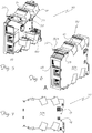
- Each slave module 10 and master module 20 further comprises means for electrical connection to adjacent slave/master modules for transmitting the power and earthing sources for power supply of the control circuits; for this purpose ( Fig. 7 ), the printed circuit 30 comprises female connectors accessible from outside the container and suitable for connection to conducting strips 50a of jumpers 50 ( Fig. 3,9 ).
- the insertion of the jumpers 50 in the respective female connector 35 gives rise to both an electrical series connection of two adjacent terminal blocks and a mechanical connection between them, ensuring their stability and rigidity.
- the female connectors 35 of the printed circuit are provided on different opposite sides of the terminal block so as to define in an unambiguous manner the power line (Volt) and the earth line (GND), thus avoiding connection errors which could result in damaging short-circuits.
- the master terminal block is designed to generate optical data signals and to transmit by means of a jumper 50 an electric power supply, received for instance from a wire connected to the electrical connector 21, to the single slave modules 10, for powering thereof; these latter are able to receive and process data signals assigned to them and/or forward to other slaves modules the data signals emitted by the master device and not assigned to them and/or transmit an electric power supply to adjacent terminal blocks by means of a jumper.
- the modules according to the invention which are shown by way of example in the form of a terminal block, have a rear end face provided with hook and spring means for mounting on DIN switchboard rails 6.
- the switchboard terminal blocks according to the invention for the transmission of data by means of optical signals allow connection together of the various modules by means of simple contact of the respective adjacent side surfaces, said contact bringing the respective optical receiver/transmitter means of each side of the printed circuit into alignment with the transmitter/receiver means of the other module, resulting in two different transmission and reception channels along which the optical signals travel, thus being able to eliminate the drawbacks of the prior art and in particular the need for a large number of electrical contacts.
- optical transmission modules according to the invention also results in the substantial elimination of the mechanical disturbances resulting from vibrations and electromagnetic disturbances resulting the connector connections of the prior art, having moreover small dimensions, being easy and inexpensive to produce and assemble, not being prone to wear and being able to be installed easily in any user location using normal standardized connection means.
- each slave module 10 or master module 20 comprises indicators 16,26 for indicating an enable/disabled condition, for example consisting of LEDs which may optionally be differently coloured, for indicating the different condition/state of the module; preferably the indicators are arranged according to different alignments for the master and slave devices.
- a further advantage arising from the configuration of the modules according to the invention is the elimination of any errors in the connection between adjacent modules; the asymmetrical configuration of the windows 13,14 of the half-shells 10a,10b 20a,20b provides an unambiguous guide for the user.
- the master terminal block may be arranged on either one of the opposite ends of the DIN rail, but also in an intermediate position between several slave terminal blocks arranged on opposite sides of the master module in the transverse direction Y-Y parallel to which propagation of the optical data signal occurs.
Landscapes
- Engineering & Computer Science (AREA)
- Microelectronics & Electronic Packaging (AREA)
- Physics & Mathematics (AREA)
- Electromagnetism (AREA)
- Computer Networks & Wireless Communication (AREA)
- Signal Processing (AREA)
- Optics & Photonics (AREA)
- Automation & Control Theory (AREA)
- General Physics & Mathematics (AREA)
- Optical Communication System (AREA)
Abstract
and a rear end face provided with hook and spring means for mounting on a DIN switchboard rail (6);
wherein the printed circuit (30) carries:
- means (60) for electrical-optical conversion and/or vice versa;
- at least one first receiver/transmitter pair (33) comprising a first transmitter device (33a) on one of the two opposite sides and a first receiver device (33b) on the other of the two sides, situated opposite each other, for propagating respective optical signals (2) in a first flow direction parallel to the transverse direction (Y-Y) ;
- at least one second transmitter/receiver pair (34) comprising a second transmitter device (34a) on the side on which the first receiver (33b) is arranged and a second receiver device (34b) on the side on which the first transmitter (33a) is arranged, situated opposite each other in a second direction of propagation of optical signals parallel to the transverse direction (Y-Y), each side surface (10a,20a) of the container (10,20) having an associated reception window (13) and a transmission window (14) respectively arranged in alignment with the said receiver/transmitter devices (33a,33b;34a,34b) on the opposite sides (30a,30b) of the printed circuit (30).
Description
- The present invention relates to a modular switchboard terminal block having means for the reception and transmission of optical signals.
- In the technical sector of process control so-called distributed I/O connection systems for the transmission of data signals are known, these being essentially formed (see
Fig. 1 ) by a plurality of slave elements arranged in the vicinity of thelocal detection devices 3 and/or peripheral devices to be controlled - such as temperature sensors and/or printers and the like for acquiring/emitting electrical data signals 2 from/to the said devices - and by afurther element 4, called master element, which is designed to be connected by means of predefined protocols, e.g. of the Ethernet type, to a data collection and processing device 5 which is normally remote and also to send/receive data signals to/from the slave devices. - It is also known that, in a non-exclusive embodiment, these data acquisition/emission elements may be formed as switchboard terminal blocks, that are devices having terminals for connecting with electric wires.
- The connection between the various known terminal blocks is of the electrical type and involves the connection of each of them to a common distribution board by means of special contacts and wiring cables, so-called buses, which give rise to a series of technical problems due to the need to provide the contacts on each element and on the distribution board and also because of their sensitivity to electromagnetic disturbances, which are particularly significant in the case of management of both digital and analog low-voltage data signals.
- Furthermore, mechanical disturbances are originated as a consequence of the vibrations that are generated within the switchboard, these disturbances greatly penalize the efficiency of the electrical contacts.
- The high number of contacts needed to provide a distributed network therefore gives rise to corresponding high costs for production and management of the different types of contact systems and therefore for storage and distribution, as well as a high probability of transmission errors, due to the said electromagnetic disturbances and mechanical disturbances, and also due to the wear affecting the known terminal blocks.
- Also known in the art are optical connectors for optical fibres and the like which are designed for reception and transmission of optical signals; examples of these devices are for example described in
US 2016/0191166 andUS 2004/0218288 . - The technical problem which is posed therefore is that of providing a modular switchboard terminal block which is able to acquire/distribute data signals, in particular, but not exclusively, for distributed networks and which is able to eliminate the drawbacks of the prior art and in particular the need for a large number of electrical contacts and the sensitivity to electromagnetic and/or mechanical disturbances.
- In connection with this problem it is also required that this modular terminal block should be able to transmit a power supply, should have small dimensions, be easy and inexpensive to produce and assemble and be able to be easily installed at any user location using normal standardized connection means.
- These results are achieved according to the present invention by a modular switchboard terminal block provided with optical means for the reception/transmission of data signals according to the characteristics features of claim 1.
- Further details may be obtained from the following description of a non-limiting example of embodiment of the subject of the present invention, provided with reference to the accompanying drawings, in which:
-
Figure 1 : shows a block diagram of a distributed I/O network configuration according to the prior art; -
Figure 2 : shows a block diagram of a distributed I/O network according to the present invention; -
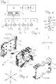
Figure 3 : shows an exploded, schematic, perspective view of a modular element according to the present invention; -
Figure 4 : shows a schematic view of the rear end face of a printed circuit with the control electronics of the modular element according to the present invention; -
Figure 5 : shows a schematic perspective view of a master modular element according to the invention in the open condition; -
Figure 6 : shows a schematic perspective view of a modular element of the master type in the closed condition; -
Figure 7 : shows a lateral the master modular element; -
Figure 8 : a front view of the master terminal block offigure 6 ; -
Figure 9 : shows a perspective view of terminal blocks according to the invention mounted on a DIN rail and electrically connected together; and -
Figure 10 : is a schematic cross-section of the assembly according toFig.9 ; - As shown in
Fig. 3 , a slavemodular element 10 or mastermodular element 20 according to the invention comprises: - a containing half-
shell - a half-
shell modular element - active
electronic circuits 60 designed for the reception and transmission of signals and/or for processing of the signals, e.g. for optical-electrical-conversion thereof and vice versa, and in the example assembled on a printedcircuit 30 inside themaster element 20 and theslave element 10; - at least one first receiver/
transmitter pair 33 for propagation of respectiveoptical signals 2, in a first flow direction parallel to the transverse direction Y-Y and comprising afirst transmitter device 33a arranged on oneside 30a of the printedcircuit 30 two opposite sides, and afirst receiver device 33b arranged on theother side 30b, and situated opposite each other; - at least one second transmitter/
receiver pair 34 for propagating respectiveoptical signals 2 in a second direction of flow parallel to the transverse direction Y-Y and comprising asecond transmitter device 34a arranged on theother side 30b on which thefirst receiver device 33b is arranged and asecond receiver device 34b arranged on theside 30a on which thefirst transmitter device 33a is arranged, situated opposite each other; said receiver/transmitter pairs 33;34 being suitably positioned at a distance from each other in the vertical direction Z-Z, so as to prevent interference between the two data transmission channels. - In this way each modular element has electronic circuits comprising a
receiver device 33b;34b and atransmitter device transmitter pair 33;34, arranged in a predefined position in the vertical direction Z-Z and in opposite directions of the transverse direction Y-Y, for example on eachside circuit 30, so as to define two different directions of propagation of the optical signals from/towards the other slavemodular elements 10 and/or mastermodular elements 20. - In a position corresponding to said receiver/transmitter devices the side surfaces of the two containing half-
shells shells respective reception window 13 and arespective transmission window 14 in the preferred example shown being respectively formed by openings which are different from each other, for example square and circular. - According to preferred aspects of the invention it is envisaged that:
- a
slave module 10 comprises (fig.9 )connectors 11 for electrical connection to (wires for input/output to/from) the various controlled and/or detection peripheral devices (not shown) for input (I) and output (O) of the electrical data signals that are processed by theslave module 10 and passed on in the direction towards the master module and from the latter to the remote processor 5 and, vice versa, from the latter to themaster element 20 and then to theslave elements 10 and to the controlled/detection devices 3 connected thereto; - a
master module 20 comprises inturn connectors 21 for electrical connection to eventual controlled/detection devices, for the input (I) / output (O) of the data signals, and/or for electrical connection towards power supply and ground sources, as well as furtherdedicated connectors 22, for connection to/from the remote processor 5; in the example shown the connectors connected to the remote processor are of the Ethernet/Ethercat type for connection by means of wiring to the said remote processor 5. - According to the invention it is therefore envisaged that the
slave module 10 and themaster module 20 are provided with respective means for transmission/propagation of optical signals, designed to propagate, in directions parallel to the transverse direction Y-Y from/toslave modules 10 connected in series and/or in line from/to themaster module 20 in turn connected in series; the optical signals being generated and/or processed by means of the printedcircuit 30circuits 60 and of downstream transducers (= input/output to the slave modules) and upstream transducers (= input/output to the remote processor) which are conventional per se and therefore not illustrated or described in detail. - Each
slave module 10 andmaster module 20 further comprises means for electrical connection to adjacent slave/master modules for transmitting the power and earthing sources for power supply of the control circuits; for this purpose (Fig. 7 ), the printedcircuit 30 comprises female connectors accessible from outside the container and suitable for connection to conductingstrips 50a of jumpers 50 (Fig. 3,9 ). - As shown, the insertion of the
jumpers 50 in the respectivefemale connector 35 gives rise to both an electrical series connection of two adjacent terminal blocks and a mechanical connection between them, ensuring their stability and rigidity. - In a preferred embodiment, the
female connectors 35 of the printed circuit are provided on different opposite sides of the terminal block so as to define in an unambiguous manner the power line (Volt) and the earth line (GND), thus avoiding connection errors which could result in damaging short-circuits. - In addition to the above it is preferred to arrange the electric power supply lines in a position at a distance from the optical transmission lines in the vertical direction Z-Z in order to prevent an eventual interference, cause of disturbances. According to the invention it is envisaged that the master terminal block is designed to generate optical data signals and to transmit by means of a
jumper 50 an electric power supply, received for instance from a wire connected to theelectrical connector 21, to thesingle slave modules 10, for powering thereof; these latter are able to receive and process data signals assigned to them and/or forward to other slaves modules the data signals emitted by the master device and not assigned to them and/or transmit an electric power supply to adjacent terminal blocks by means of a jumper. Preferably, the modules according to the invention, which are shown by way of example in the form of a terminal block, have a rear end face provided with hook and spring means for mounting on DIN switchboard rails 6. - With this configuration of modular switchboard terminal blocks of the
slave type 10 andmaster type 20, it is possible to provide distributed data communication networks, operation of which is based on the transmission of optical signals which will comprise an addressing part intended to specify thedestination module slave modules 10 to themaster module 20 or vice versa is intended; if, along the travel path, the signal encounters the destination slave or master module, it is recognized by the latter and the control electronics forward it, following optical-electric conversion, to the final destination (controlled/detection) device; if instead the signal is not recognized as assigned to theslave 10, it is transmitted to thetransmitter - It is therefore clear how the switchboard terminal blocks according to the invention for the transmission of data by means of optical signals allow connection together of the various modules by means of simple contact of the respective adjacent side surfaces, said contact bringing the respective optical receiver/transmitter means of each side of the printed circuit into alignment with the transmitter/receiver means of the other module, resulting in two different transmission and reception channels along which the optical signals travel, thus being able to eliminate the drawbacks of the prior art and in particular the need for a large number of electrical contacts.
- In addition to this the use of optical transmission modules according to the invention also results in the substantial elimination of the mechanical disturbances resulting from vibrations and electromagnetic disturbances resulting the connector connections of the prior art, having moreover small dimensions, being easy and inexpensive to produce and assemble, not being prone to wear and being able to be installed easily in any user location using normal standardized connection means.
- Preferably, each
slave module 10 ormaster module 20 comprisesindicators - A further advantage arising from the configuration of the modules according to the invention is the elimination of any errors in the connection between adjacent modules; the asymmetrical configuration of the
windows shells 10b - In addition to the above, owing to the particular configuration with two opposite sides, the master terminal block may be arranged on either one of the opposite ends of the DIN rail, but also in an intermediate position between several slave terminal blocks arranged on opposite sides of the master module in the transverse direction Y-Y parallel to which propagation of the optical data signal occurs.
- Although described in connection with a number of embodiments and a number of preferred examples of embodiment of the invention, it is understood that the scope of protection of the present patent is determined solely by the claims below.
Claims (13)
- Modular switchboard terminal block (10,20) for transmission of data signals (2), comprising a container (10a,20a) having at least two side surfaces (10b,20b) situated parallel and opposite each other in a transverse direction (Y-Y) and having, arranged inside them, a printed circuit (30) for processing the data signals, which has two opposite sides (30a,30b) in the same transverse direction (Y-Y);
Connectors (11;21) for electrical connection to controlled/detection devices, for input (I) and output (O) of electrical data signals received/transmitted from/to the devices, and/or for electrical connection to a power/ground supply source;
And a rear end face provided with hook and spring means for mounting on a DIN switchboard rail (6); characterized in that said printed circuit (30) has, mounted thereon:- means (60) for electrical-optical conversion and/or vice versa;- at least one first receiver/transmitter pair (33) comprising a first transmitter device (33a) on one of the two opposite sides and a first receiver device (33b) on the other of the two sides, situated opposite each other, for propagating respective optical signals (2) in a first flow direction parallel to the transverse direction (Y-Y) ;- at least one second transmitter/receiver pair (34) comprising a second transmitter device (34a) on the side on which the first receiver (33b) is arranged and a second receiver device (34b) on the side on which the first transmitter (33a) is arranged, situated opposite each other in a second direction of propagation of optical signals parallel to the transverse direction (Y-Y), each side surface (10a,20a) of the container (10,20) having an associated reception window (13) and a transmission window (14) respectively arranged in alignment with the said receiver/transmitter devices (33a,33b;34a,34b) on the opposite sides (30a,30b) of the printed circuit (30). - Modular terminal block according to Claim 1, characterized in that it comprises means for performing electrical connection to a terminal block adjacent in the transverse direction (Y-Y), for connection towards power sources and earthing for the power supply of the circuits.
- Modular terminal block according to Claim 2, characterized in that said electrical connection means comprise female connectors (35) arranged on the printed circuit (30) and accessible from outside the container (10;20), for coupling with a respective conducting strip (50a) of a jumper (50).
- Modular terminal block according to Claim 1, 2 or 3 characterized in that the container comprises a half-shell (10a,20a) for containing and a half-shell (10b,20b) for laterally closing the modular element (10,20), inside which the said printed circuit (30) is housed.
- Modular terminal block according to any one of the preceding claims, characterized in that it comprises indicators (16,26) for indicating an operating condition.
- Modular terminal block according to Claim 5, characterized in that said indicators (16,26) are formed by differently coloured LEDs suitable for indicating the different condition of the module.
- Modular terminal block according to any one of the preceding claims, characterized in that it comprises an Ethernet or ethercat connector (22) for connecting to an external processing unit (5).
- Modular terminal block according to claim 7 characterized in that it is of the master type, designed to generate/transmit/receive optical signals (2), to connect to an electric power supply/ground source and to connect to an external processing unit (5).
- Modular terminal block according to any one of the preceding claims 1-6, characterized in that it is of the slave type, designed to receive/transmit/forward optical signals (2) and to receive/transmit electrical signals from/to controlled/detection devices connected thereto.
- Distributed I/O network for the transmission of data signals (2) from/to local detection devices and/or peripheral units to be controlled, characterized in that it comprises at least two modular terminal blocks according to any Claim 1-9, arranged adjacent each other in the transver direction (Y-Y).
- Distributed I/O network according to Claim 10, characterized in that the terminal blocks are arranged along a same DIN rail (6).
- Distributed I/O network according to Claim 10 or 11, characterized in that it comprises a terminal block of the master type and one or more slave terminal blocks adjacent.
- Distributed I/O network according to Claim 10, 11 or 12 characterized in that the adjacent terminal blocks are electrically connected by means of jumpers (50).
Priority Applications (1)
| Application Number | Priority Date | Filing Date | Title |
|---|---|---|---|
| PL17167212T PL3239751T3 (en) | 2016-04-22 | 2017-04-20 | Modular switchboard terminal block with means for transmission of optical data signals |
Applications Claiming Priority (1)
| Application Number | Priority Date | Filing Date | Title |
|---|---|---|---|
| ITUA2016A002828A ITUA20162828A1 (en) | 2016-04-22 | 2016-04-22 | MODULAR CONNECTION ELEMENT WITH OPTICAL MEANS FOR DATA TRANSMISSION |
Publications (2)
| Publication Number | Publication Date |
|---|---|
| EP3239751A1 true EP3239751A1 (en) | 2017-11-01 |
| EP3239751B1 EP3239751B1 (en) | 2019-09-04 |
Family
ID=56684145
Family Applications (1)
| Application Number | Title | Priority Date | Filing Date |
|---|---|---|---|
| EP17167212.4A Active EP3239751B1 (en) | 2016-04-22 | 2017-04-20 | Modular switchboard terminal block with means for transmission of optical data signals |
Country Status (4)
| Country | Link |
|---|---|
| US (1) | US10187709B2 (en) |
| EP (1) | EP3239751B1 (en) |
| IT (1) | ITUA20162828A1 (en) |
| PL (1) | PL3239751T3 (en) |
Families Citing this family (2)
| Publication number | Priority date | Publication date | Assignee | Title |
|---|---|---|---|---|
| TWI697161B (en) * | 2018-03-09 | 2020-06-21 | 町洋企業股份有限公司 | System comprising multiple functional modules and addressing method for functional modules thereof |
| CN112968523A (en) * | 2021-02-23 | 2021-06-15 | 珠海万力达电气自动化有限公司 | Modularized intelligent power distribution terminal and self-healing control method thereof |
Citations (3)
| Publication number | Priority date | Publication date | Assignee | Title |
|---|---|---|---|---|
| US20040218288A1 (en) | 2003-05-02 | 2004-11-04 | International Business Machines Corporation | Optical communication assembly |
| US20090269075A1 (en) * | 2008-04-24 | 2009-10-29 | Avago Technologies Fiber Ip Pte. Ltd. | Electro-optical assembly and method for making an electro-optical assembly |
| CN104503044A (en) * | 2014-12-31 | 2015-04-08 | 苏州旭创科技有限公司 | Optical module |
Family Cites Families (1)
| Publication number | Priority date | Publication date | Assignee | Title |
|---|---|---|---|---|
| US9170387B2 (en) * | 2011-09-29 | 2015-10-27 | Corning Cable Systems Llc | Optical component assemblies |
-
2016
- 2016-04-22 IT ITUA2016A002828A patent/ITUA20162828A1/en unknown
-
2017
- 2017-04-20 EP EP17167212.4A patent/EP3239751B1/en active Active
- 2017-04-20 PL PL17167212T patent/PL3239751T3/en unknown
- 2017-04-21 US US15/493,530 patent/US10187709B2/en active Active
Patent Citations (4)
| Publication number | Priority date | Publication date | Assignee | Title |
|---|---|---|---|---|
| US20040218288A1 (en) | 2003-05-02 | 2004-11-04 | International Business Machines Corporation | Optical communication assembly |
| US20090269075A1 (en) * | 2008-04-24 | 2009-10-29 | Avago Technologies Fiber Ip Pte. Ltd. | Electro-optical assembly and method for making an electro-optical assembly |
| CN104503044A (en) * | 2014-12-31 | 2015-04-08 | 苏州旭创科技有限公司 | Optical module |
| US20160191166A1 (en) | 2014-12-31 | 2016-06-30 | Innolight Technology Corporation | Optical Module |
Also Published As
| Publication number | Publication date |
|---|---|
| ITUA20162828A1 (en) | 2017-10-22 |
| PL3239751T3 (en) | 2020-04-30 |
| US10187709B2 (en) | 2019-01-22 |
| EP3239751B1 (en) | 2019-09-04 |
| US20170311057A1 (en) | 2017-10-26 |
Similar Documents
| Publication | Publication Date | Title |
|---|---|---|
| US10980145B2 (en) | Hot-pluggable connection for data communications | |
| US9007206B2 (en) | Patch panel and intelligent structured cabling system | |
| RU2012106349A (en) | PANEL ASSEMBLY FOR NETWORK INTERACTION MANAGEMENT SYSTEM | |
| EP2412169A1 (en) | Physical layer management for interconnect configurations using rfid chip technology | |
| CN103718658A (en) | Backboard, insert frame and network equipment | |
| EP3239751B1 (en) | Modular switchboard terminal block with means for transmission of optical data signals | |
| RU2012128525A (en) | INPUT / OUTPUT MODULE | |
| CN112005530A (en) | But hot plug's no cable contact switch casing | |
| US20210298194A1 (en) | Power distribution unit with a modular construction | |
| US8565611B2 (en) | Optically-connected system for exchanging data among industrial automation devices | |
| EP3157039B1 (en) | Communicating circuit breaker architecture with automatic load center position identification | |
| US10483664B2 (en) | Electronic terminal block for a data bus | |
| EP1332570B1 (en) | Network comprising converters between electrical and optical signals | |
| TWI436534B (en) | Intelligent structured cabling system and jack | |
| EP1891528B1 (en) | Apparatus and method for monitoring connectivity status of communication ports | |
| CA2431273C (en) | Optical connection system | |
| KR20160000347A (en) | Optical interface apparatus | |
| CN211404856U (en) | Electrical connection device | |
| JP2711985B2 (en) | Connector unit and connector unit module | |
| JPS6264141A (en) | In-frame mounting system | |
| JPH0652952A (en) | Data bus network system | |
| JPH0563958B2 (en) | ||
| KR20140125537A (en) | Patch Cord, Patch Panel And Management System Having The Same |
Legal Events
| Date | Code | Title | Description |
|---|---|---|---|
| PUAI | Public reference made under article 153(3) epc to a published international application that has entered the european phase |
Free format text: ORIGINAL CODE: 0009012 |
|
| STAA | Information on the status of an ep patent application or granted ep patent |
Free format text: STATUS: THE APPLICATION HAS BEEN PUBLISHED |
|
| AK | Designated contracting states |
Kind code of ref document: A1 Designated state(s): AL AT BE BG CH CY CZ DE DK EE ES FI FR GB GR HR HU IE IS IT LI LT LU LV MC MK MT NL NO PL PT RO RS SE SI SK SM TR |
|
| AX | Request for extension of the european patent |
Extension state: BA ME |
|
| STAA | Information on the status of an ep patent application or granted ep patent |
Free format text: STATUS: REQUEST FOR EXAMINATION WAS MADE |
|
| 17P | Request for examination filed |
Effective date: 20180427 |
|
| RBV | Designated contracting states (corrected) |
Designated state(s): AL AT BE BG CH CY CZ DE DK EE ES FI FR GB GR HR HU IE IS IT LI LT LU LV MC MK MT NL NO PL PT RO RS SE SI SK SM TR |
|
| GRAP | Despatch of communication of intention to grant a patent |
Free format text: ORIGINAL CODE: EPIDOSNIGR1 |
|
| STAA | Information on the status of an ep patent application or granted ep patent |
Free format text: STATUS: GRANT OF PATENT IS INTENDED |
|
| INTG | Intention to grant announced |
Effective date: 20190425 |
|
| GRAS | Grant fee paid |
Free format text: ORIGINAL CODE: EPIDOSNIGR3 |
|
| GRAA | (expected) grant |
Free format text: ORIGINAL CODE: 0009210 |
|
| STAA | Information on the status of an ep patent application or granted ep patent |
Free format text: STATUS: THE PATENT HAS BEEN GRANTED |
|
| AK | Designated contracting states |
Kind code of ref document: B1 Designated state(s): AL AT BE BG CH CY CZ DE DK EE ES FI FR GB GR HR HU IE IS IT LI LT LU LV MC MK MT NL NO PL PT RO RS SE SI SK SM TR |
|
| REG | Reference to a national code |
Ref country code: GB Ref legal event code: FG4D |
|
| REG | Reference to a national code |
Ref country code: CH Ref legal event code: EP |
|
| REG | Reference to a national code |
Ref country code: AT Ref legal event code: REF Ref document number: 1176163 Country of ref document: AT Kind code of ref document: T Effective date: 20190915 |
|
| REG | Reference to a national code |
Ref country code: DE Ref legal event code: R096 Ref document number: 602017006644 Country of ref document: DE |
|
| REG | Reference to a national code |
Ref country code: IE Ref legal event code: FG4D |
|
| REG | Reference to a national code |
Ref country code: CH Ref legal event code: NV Representative=s name: DR. LUSUARDI AG, CH |
|
| REG | Reference to a national code |
Ref country code: NL Ref legal event code: MP Effective date: 20190904 |
|
| REG | Reference to a national code |
Ref country code: LT Ref legal event code: MG4D |
|
| PG25 | Lapsed in a contracting state [announced via postgrant information from national office to epo] |
Ref country code: BG Free format text: LAPSE BECAUSE OF FAILURE TO SUBMIT A TRANSLATION OF THE DESCRIPTION OR TO PAY THE FEE WITHIN THE PRESCRIBED TIME-LIMIT Effective date: 20191204 Ref country code: LT Free format text: LAPSE BECAUSE OF FAILURE TO SUBMIT A TRANSLATION OF THE DESCRIPTION OR TO PAY THE FEE WITHIN THE PRESCRIBED TIME-LIMIT Effective date: 20190904 Ref country code: HR Free format text: LAPSE BECAUSE OF FAILURE TO SUBMIT A TRANSLATION OF THE DESCRIPTION OR TO PAY THE FEE WITHIN THE PRESCRIBED TIME-LIMIT Effective date: 20190904 Ref country code: SE Free format text: LAPSE BECAUSE OF FAILURE TO SUBMIT A TRANSLATION OF THE DESCRIPTION OR TO PAY THE FEE WITHIN THE PRESCRIBED TIME-LIMIT Effective date: 20190904 Ref country code: FI Free format text: LAPSE BECAUSE OF FAILURE TO SUBMIT A TRANSLATION OF THE DESCRIPTION OR TO PAY THE FEE WITHIN THE PRESCRIBED TIME-LIMIT Effective date: 20190904 Ref country code: NO Free format text: LAPSE BECAUSE OF FAILURE TO SUBMIT A TRANSLATION OF THE DESCRIPTION OR TO PAY THE FEE WITHIN THE PRESCRIBED TIME-LIMIT Effective date: 20191204 |
|
| PG25 | Lapsed in a contracting state [announced via postgrant information from national office to epo] |
Ref country code: ES Free format text: LAPSE BECAUSE OF FAILURE TO SUBMIT A TRANSLATION OF THE DESCRIPTION OR TO PAY THE FEE WITHIN THE PRESCRIBED TIME-LIMIT Effective date: 20190904 Ref country code: RS Free format text: LAPSE BECAUSE OF FAILURE TO SUBMIT A TRANSLATION OF THE DESCRIPTION OR TO PAY THE FEE WITHIN THE PRESCRIBED TIME-LIMIT Effective date: 20190904 Ref country code: GR Free format text: LAPSE BECAUSE OF FAILURE TO SUBMIT A TRANSLATION OF THE DESCRIPTION OR TO PAY THE FEE WITHIN THE PRESCRIBED TIME-LIMIT Effective date: 20191205 Ref country code: LV Free format text: LAPSE BECAUSE OF FAILURE TO SUBMIT A TRANSLATION OF THE DESCRIPTION OR TO PAY THE FEE WITHIN THE PRESCRIBED TIME-LIMIT Effective date: 20190904 Ref country code: AL Free format text: LAPSE BECAUSE OF FAILURE TO SUBMIT A TRANSLATION OF THE DESCRIPTION OR TO PAY THE FEE WITHIN THE PRESCRIBED TIME-LIMIT Effective date: 20190904 |
|
| REG | Reference to a national code |
Ref country code: AT Ref legal event code: MK05 Ref document number: 1176163 Country of ref document: AT Kind code of ref document: T Effective date: 20190904 |
|
| PG25 | Lapsed in a contracting state [announced via postgrant information from national office to epo] |
Ref country code: RO Free format text: LAPSE BECAUSE OF FAILURE TO SUBMIT A TRANSLATION OF THE DESCRIPTION OR TO PAY THE FEE WITHIN THE PRESCRIBED TIME-LIMIT Effective date: 20190904 Ref country code: PT Free format text: LAPSE BECAUSE OF FAILURE TO SUBMIT A TRANSLATION OF THE DESCRIPTION OR TO PAY THE FEE WITHIN THE PRESCRIBED TIME-LIMIT Effective date: 20200106 Ref country code: EE Free format text: LAPSE BECAUSE OF FAILURE TO SUBMIT A TRANSLATION OF THE DESCRIPTION OR TO PAY THE FEE WITHIN THE PRESCRIBED TIME-LIMIT Effective date: 20190904 Ref country code: AT Free format text: LAPSE BECAUSE OF FAILURE TO SUBMIT A TRANSLATION OF THE DESCRIPTION OR TO PAY THE FEE WITHIN THE PRESCRIBED TIME-LIMIT Effective date: 20190904 Ref country code: NL Free format text: LAPSE BECAUSE OF FAILURE TO SUBMIT A TRANSLATION OF THE DESCRIPTION OR TO PAY THE FEE WITHIN THE PRESCRIBED TIME-LIMIT Effective date: 20190904 |
|
| PG25 | Lapsed in a contracting state [announced via postgrant information from national office to epo] |
Ref country code: IS Free format text: LAPSE BECAUSE OF FAILURE TO SUBMIT A TRANSLATION OF THE DESCRIPTION OR TO PAY THE FEE WITHIN THE PRESCRIBED TIME-LIMIT Effective date: 20200224 Ref country code: SK Free format text: LAPSE BECAUSE OF FAILURE TO SUBMIT A TRANSLATION OF THE DESCRIPTION OR TO PAY THE FEE WITHIN THE PRESCRIBED TIME-LIMIT Effective date: 20190904 Ref country code: SM Free format text: LAPSE BECAUSE OF FAILURE TO SUBMIT A TRANSLATION OF THE DESCRIPTION OR TO PAY THE FEE WITHIN THE PRESCRIBED TIME-LIMIT Effective date: 20190904 Ref country code: CZ Free format text: LAPSE BECAUSE OF FAILURE TO SUBMIT A TRANSLATION OF THE DESCRIPTION OR TO PAY THE FEE WITHIN THE PRESCRIBED TIME-LIMIT Effective date: 20190904 |
|
| REG | Reference to a national code |
Ref country code: DE Ref legal event code: R097 Ref document number: 602017006644 Country of ref document: DE |
|
| PLBE | No opposition filed within time limit |
Free format text: ORIGINAL CODE: 0009261 |
|
| STAA | Information on the status of an ep patent application or granted ep patent |
Free format text: STATUS: NO OPPOSITION FILED WITHIN TIME LIMIT |
|
| PG2D | Information on lapse in contracting state deleted |
Ref country code: IS |
|
| PG25 | Lapsed in a contracting state [announced via postgrant information from national office to epo] |
Ref country code: DK Free format text: LAPSE BECAUSE OF FAILURE TO SUBMIT A TRANSLATION OF THE DESCRIPTION OR TO PAY THE FEE WITHIN THE PRESCRIBED TIME-LIMIT Effective date: 20190904 Ref country code: IS Free format text: LAPSE BECAUSE OF FAILURE TO SUBMIT A TRANSLATION OF THE DESCRIPTION OR TO PAY THE FEE WITHIN THE PRESCRIBED TIME-LIMIT Effective date: 20200105 |
|
| 26N | No opposition filed |
Effective date: 20200605 |
|
| PG25 | Lapsed in a contracting state [announced via postgrant information from national office to epo] |
Ref country code: SI Free format text: LAPSE BECAUSE OF FAILURE TO SUBMIT A TRANSLATION OF THE DESCRIPTION OR TO PAY THE FEE WITHIN THE PRESCRIBED TIME-LIMIT Effective date: 20190904 |
|
| PG25 | Lapsed in a contracting state [announced via postgrant information from national office to epo] |
Ref country code: MC Free format text: LAPSE BECAUSE OF FAILURE TO SUBMIT A TRANSLATION OF THE DESCRIPTION OR TO PAY THE FEE WITHIN THE PRESCRIBED TIME-LIMIT Effective date: 20190904 |
|
| PG25 | Lapsed in a contracting state [announced via postgrant information from national office to epo] |
Ref country code: LU Free format text: LAPSE BECAUSE OF NON-PAYMENT OF DUE FEES Effective date: 20200420 |
|
| REG | Reference to a national code |
Ref country code: BE Ref legal event code: MM Effective date: 20200430 |
|
| PG25 | Lapsed in a contracting state [announced via postgrant information from national office to epo] |
Ref country code: BE Free format text: LAPSE BECAUSE OF NON-PAYMENT OF DUE FEES Effective date: 20200430 |
|
| PG25 | Lapsed in a contracting state [announced via postgrant information from national office to epo] |
Ref country code: IE Free format text: LAPSE BECAUSE OF NON-PAYMENT OF DUE FEES Effective date: 20200420 |
|
| PG25 | Lapsed in a contracting state [announced via postgrant information from national office to epo] |
Ref country code: TR Free format text: LAPSE BECAUSE OF FAILURE TO SUBMIT A TRANSLATION OF THE DESCRIPTION OR TO PAY THE FEE WITHIN THE PRESCRIBED TIME-LIMIT Effective date: 20190904 Ref country code: MT Free format text: LAPSE BECAUSE OF FAILURE TO SUBMIT A TRANSLATION OF THE DESCRIPTION OR TO PAY THE FEE WITHIN THE PRESCRIBED TIME-LIMIT Effective date: 20190904 Ref country code: CY Free format text: LAPSE BECAUSE OF FAILURE TO SUBMIT A TRANSLATION OF THE DESCRIPTION OR TO PAY THE FEE WITHIN THE PRESCRIBED TIME-LIMIT Effective date: 20190904 |
|
| PG25 | Lapsed in a contracting state [announced via postgrant information from national office to epo] |
Ref country code: MK Free format text: LAPSE BECAUSE OF FAILURE TO SUBMIT A TRANSLATION OF THE DESCRIPTION OR TO PAY THE FEE WITHIN THE PRESCRIBED TIME-LIMIT Effective date: 20190904 |
|
| REG | Reference to a national code |
Ref country code: DE Ref legal event code: R082 Ref document number: 602017006644 Country of ref document: DE Representative=s name: SKM-IP SCHMID KRAUSS KUTTENKEULER MALESCHA SCH, DE |
|
| P01 | Opt-out of the competence of the unified patent court (upc) registered |
Effective date: 20230518 |
|
| PGFP | Annual fee paid to national office [announced via postgrant information from national office to epo] |
Ref country code: GB Payment date: 20240409 Year of fee payment: 8 |
|
| PGFP | Annual fee paid to national office [announced via postgrant information from national office to epo] |
Ref country code: DE Payment date: 20240409 Year of fee payment: 8 |
|
| PGFP | Annual fee paid to national office [announced via postgrant information from national office to epo] |
Ref country code: CH Payment date: 20240501 Year of fee payment: 8 |
|
| PGFP | Annual fee paid to national office [announced via postgrant information from national office to epo] |
Ref country code: IT Payment date: 20240424 Year of fee payment: 8 Ref country code: FR Payment date: 20240409 Year of fee payment: 8 |
|
| PGFP | Annual fee paid to national office [announced via postgrant information from national office to epo] |
Ref country code: PL Payment date: 20240415 Year of fee payment: 8 |