EP3236533A1 - Module-terminal block connection structure and connection method - Google Patents
Module-terminal block connection structure and connection method Download PDFInfo
- Publication number
- EP3236533A1 EP3236533A1 EP15869683.1A EP15869683A EP3236533A1 EP 3236533 A1 EP3236533 A1 EP 3236533A1 EP 15869683 A EP15869683 A EP 15869683A EP 3236533 A1 EP3236533 A1 EP 3236533A1
- Authority
- EP
- European Patent Office
- Prior art keywords
- terminal block
- module
- wiring board
- printed wiring
- lead pin
- Prior art date
- Legal status (The legal status is an assumption and is not a legal conclusion. Google has not performed a legal analysis and makes no representation as to the accuracy of the status listed.)
- Withdrawn
Links
- 238000000034 method Methods 0.000 title claims description 19
- 239000004020 conductor Substances 0.000 claims abstract description 5
- RYGMFSIKBFXOCR-UHFFFAOYSA-N Copper Chemical compound [Cu] RYGMFSIKBFXOCR-UHFFFAOYSA-N 0.000 claims description 30
- 229910052802 copper Inorganic materials 0.000 claims description 30
- 239000010949 copper Substances 0.000 claims description 30
- 238000005476 soldering Methods 0.000 description 7
- 238000004519 manufacturing process Methods 0.000 description 6
- 230000017525 heat dissipation Effects 0.000 description 5
- 238000009413 insulation Methods 0.000 description 5
- 230000005855 radiation Effects 0.000 description 4
- 230000000694 effects Effects 0.000 description 3
- 239000003990 capacitor Substances 0.000 description 2
- 238000010586 diagram Methods 0.000 description 2
- 238000004806 packaging method and process Methods 0.000 description 2
- 238000005192 partition Methods 0.000 description 2
- 230000035515 penetration Effects 0.000 description 1
- 230000002093 peripheral effect Effects 0.000 description 1
- 239000011347 resin Substances 0.000 description 1
- 229920005989 resin Polymers 0.000 description 1
- 229910000679 solder Inorganic materials 0.000 description 1
Images



Classifications
-
- H—ELECTRICITY
- H01—ELECTRIC ELEMENTS
- H01R—ELECTRICALLY-CONDUCTIVE CONNECTIONS; STRUCTURAL ASSOCIATIONS OF A PLURALITY OF MUTUALLY-INSULATED ELECTRICAL CONNECTING ELEMENTS; COUPLING DEVICES; CURRENT COLLECTORS
- H01R12/00—Structural associations of a plurality of mutually-insulated electrical connecting elements, specially adapted for printed circuits, e.g. printed circuit boards [PCB], flat or ribbon cables, or like generally planar structures, e.g. terminal strips, terminal blocks; Coupling devices specially adapted for printed circuits, flat or ribbon cables, or like generally planar structures; Terminals specially adapted for contact with, or insertion into, printed circuits, flat or ribbon cables, or like generally planar structures
- H01R12/50—Fixed connections
- H01R12/51—Fixed connections for rigid printed circuits or like structures
- H01R12/515—Terminal blocks providing connections to wires or cables
-
- H—ELECTRICITY
- H01—ELECTRIC ELEMENTS
- H01R—ELECTRICALLY-CONDUCTIVE CONNECTIONS; STRUCTURAL ASSOCIATIONS OF A PLURALITY OF MUTUALLY-INSULATED ELECTRICAL CONNECTING ELEMENTS; COUPLING DEVICES; CURRENT COLLECTORS
- H01R12/00—Structural associations of a plurality of mutually-insulated electrical connecting elements, specially adapted for printed circuits, e.g. printed circuit boards [PCB], flat or ribbon cables, or like generally planar structures, e.g. terminal strips, terminal blocks; Coupling devices specially adapted for printed circuits, flat or ribbon cables, or like generally planar structures; Terminals specially adapted for contact with, or insertion into, printed circuits, flat or ribbon cables, or like generally planar structures
- H01R12/50—Fixed connections
- H01R12/51—Fixed connections for rigid printed circuits or like structures
- H01R12/55—Fixed connections for rigid printed circuits or like structures characterised by the terminals
- H01R12/58—Fixed connections for rigid printed circuits or like structures characterised by the terminals terminals for insertion into holes
- H01R12/585—Terminals having a press fit or a compliant portion and a shank passing through a hole in the printed circuit board
-
- H—ELECTRICITY
- H01—ELECTRIC ELEMENTS
- H01R—ELECTRICALLY-CONDUCTIVE CONNECTIONS; STRUCTURAL ASSOCIATIONS OF A PLURALITY OF MUTUALLY-INSULATED ELECTRICAL CONNECTING ELEMENTS; COUPLING DEVICES; CURRENT COLLECTORS
- H01R4/00—Electrically-conductive connections between two or more conductive members in direct contact, i.e. touching one another; Means for effecting or maintaining such contact; Electrically-conductive connections having two or more spaced connecting locations for conductors and using contact members penetrating insulation
- H01R4/24—Connections using contact members penetrating or cutting insulation or cable strands
- H01R4/2416—Connections using contact members penetrating or cutting insulation or cable strands the contact members having insulation-cutting edges, e.g. of tuning fork type
- H01R4/242—Connections using contact members penetrating or cutting insulation or cable strands the contact members having insulation-cutting edges, e.g. of tuning fork type the contact members being plates having a single slot
- H01R4/2425—Flat plates, e.g. multi-layered flat plates
- H01R4/2429—Flat plates, e.g. multi-layered flat plates mounted in an insulating base
-
- H—ELECTRICITY
- H01—ELECTRIC ELEMENTS
- H01R—ELECTRICALLY-CONDUCTIVE CONNECTIONS; STRUCTURAL ASSOCIATIONS OF A PLURALITY OF MUTUALLY-INSULATED ELECTRICAL CONNECTING ELEMENTS; COUPLING DEVICES; CURRENT COLLECTORS
- H01R4/00—Electrically-conductive connections between two or more conductive members in direct contact, i.e. touching one another; Means for effecting or maintaining such contact; Electrically-conductive connections having two or more spaced connecting locations for conductors and using contact members penetrating insulation
- H01R4/24—Connections using contact members penetrating or cutting insulation or cable strands
- H01R4/2416—Connections using contact members penetrating or cutting insulation or cable strands the contact members having insulation-cutting edges, e.g. of tuning fork type
- H01R4/2445—Connections using contact members penetrating or cutting insulation or cable strands the contact members having insulation-cutting edges, e.g. of tuning fork type the contact members having additional means acting on the insulation or the wire, e.g. additional insulation penetrating means, strain relief means or wire cutting knives
-
- H—ELECTRICITY
- H01—ELECTRIC ELEMENTS
- H01R—ELECTRICALLY-CONDUCTIVE CONNECTIONS; STRUCTURAL ASSOCIATIONS OF A PLURALITY OF MUTUALLY-INSULATED ELECTRICAL CONNECTING ELEMENTS; COUPLING DEVICES; CURRENT COLLECTORS
- H01R4/00—Electrically-conductive connections between two or more conductive members in direct contact, i.e. touching one another; Means for effecting or maintaining such contact; Electrically-conductive connections having two or more spaced connecting locations for conductors and using contact members penetrating insulation
- H01R4/24—Connections using contact members penetrating or cutting insulation or cable strands
- H01R4/2475—Connections using contact members penetrating or cutting insulation or cable strands the contact members penetrating the insulation being actuated by screws, nuts or bolts
-
- H—ELECTRICITY
- H01—ELECTRIC ELEMENTS
- H01R—ELECTRICALLY-CONDUCTIVE CONNECTIONS; STRUCTURAL ASSOCIATIONS OF A PLURALITY OF MUTUALLY-INSULATED ELECTRICAL CONNECTING ELEMENTS; COUPLING DEVICES; CURRENT COLLECTORS
- H01R4/00—Electrically-conductive connections between two or more conductive members in direct contact, i.e. touching one another; Means for effecting or maintaining such contact; Electrically-conductive connections having two or more spaced connecting locations for conductors and using contact members penetrating insulation
- H01R4/28—Clamped connections, spring connections
- H01R4/30—Clamped connections, spring connections utilising a screw or nut clamping member
- H01R4/301—Clamped connections, spring connections utilising a screw or nut clamping member having means for preventing complete unscrewing of screw or nut
-
- H—ELECTRICITY
- H01—ELECTRIC ELEMENTS
- H01R—ELECTRICALLY-CONDUCTIVE CONNECTIONS; STRUCTURAL ASSOCIATIONS OF A PLURALITY OF MUTUALLY-INSULATED ELECTRICAL CONNECTING ELEMENTS; COUPLING DEVICES; CURRENT COLLECTORS
- H01R4/00—Electrically-conductive connections between two or more conductive members in direct contact, i.e. touching one another; Means for effecting or maintaining such contact; Electrically-conductive connections having two or more spaced connecting locations for conductors and using contact members penetrating insulation
- H01R4/28—Clamped connections, spring connections
- H01R4/30—Clamped connections, spring connections utilising a screw or nut clamping member
- H01R4/34—Conductive members located under head of screw
-
- H—ELECTRICITY
- H01—ELECTRIC ELEMENTS
- H01R—ELECTRICALLY-CONDUCTIVE CONNECTIONS; STRUCTURAL ASSOCIATIONS OF A PLURALITY OF MUTUALLY-INSULATED ELECTRICAL CONNECTING ELEMENTS; COUPLING DEVICES; CURRENT COLLECTORS
- H01R4/00—Electrically-conductive connections between two or more conductive members in direct contact, i.e. touching one another; Means for effecting or maintaining such contact; Electrically-conductive connections having two or more spaced connecting locations for conductors and using contact members penetrating insulation
- H01R4/28—Clamped connections, spring connections
- H01R4/38—Clamped connections, spring connections utilising a clamping member acted on by screw or nut
-
- H—ELECTRICITY
- H05—ELECTRIC TECHNIQUES NOT OTHERWISE PROVIDED FOR
- H05K—PRINTED CIRCUITS; CASINGS OR CONSTRUCTIONAL DETAILS OF ELECTRIC APPARATUS; MANUFACTURE OF ASSEMBLAGES OF ELECTRICAL COMPONENTS
- H05K1/00—Printed circuits
- H05K1/18—Printed circuits structurally associated with non-printed electric components
-
- H—ELECTRICITY
- H01—ELECTRIC ELEMENTS
- H01R—ELECTRICALLY-CONDUCTIVE CONNECTIONS; STRUCTURAL ASSOCIATIONS OF A PLURALITY OF MUTUALLY-INSULATED ELECTRICAL CONNECTING ELEMENTS; COUPLING DEVICES; CURRENT COLLECTORS
- H01R12/00—Structural associations of a plurality of mutually-insulated electrical connecting elements, specially adapted for printed circuits, e.g. printed circuit boards [PCB], flat or ribbon cables, or like generally planar structures, e.g. terminal strips, terminal blocks; Coupling devices specially adapted for printed circuits, flat or ribbon cables, or like generally planar structures; Terminals specially adapted for contact with, or insertion into, printed circuits, flat or ribbon cables, or like generally planar structures
- H01R12/70—Coupling devices
- H01R12/7076—Coupling devices for connection between PCB and component, e.g. display
-
- H—ELECTRICITY
- H01—ELECTRIC ELEMENTS
- H01R—ELECTRICALLY-CONDUCTIVE CONNECTIONS; STRUCTURAL ASSOCIATIONS OF A PLURALITY OF MUTUALLY-INSULATED ELECTRICAL CONNECTING ELEMENTS; COUPLING DEVICES; CURRENT COLLECTORS
- H01R12/00—Structural associations of a plurality of mutually-insulated electrical connecting elements, specially adapted for printed circuits, e.g. printed circuit boards [PCB], flat or ribbon cables, or like generally planar structures, e.g. terminal strips, terminal blocks; Coupling devices specially adapted for printed circuits, flat or ribbon cables, or like generally planar structures; Terminals specially adapted for contact with, or insertion into, printed circuits, flat or ribbon cables, or like generally planar structures
- H01R12/70—Coupling devices
- H01R12/7088—Arrangements for power supply
Definitions
- the present invention relates to a connection structure and a connection method between a lead pin of a module, which is formed by packaging a predetermined electric circuit, and an external terminal block.
- an inverter in an air conditioner is formed into a power module in which necessary peripheral circuits are packaged, and this power module is attached to a printed wiring board. At that time, lead pins coming out of the power module are soldered to a copper pattern of the printed wiring board. Lead pins of a main circuit through which a current supplied to a motor flows are connected to a terminal block via the copper pattern on the board. A crimp terminal of the electric wire can be connected to the terminal block by screw clamp.
- the terminal block and other devices are disposed on, for example, a front surface of the printed wiring board, and the power module is disposed on a rear surface. The arrangement on the front and rear surfaces is convenient for attaching a radiation fin to the power module (for example, see Patent Literature 1 ( FIG. 3 )).
- Patent Literature 1 JP 2009-289734 A
- Patent Literature 1 proposes a technique of directly connecting a power module to a terminal block by using a terminal block having an extremely special shape.
- a general-purpose inexpensive terminal block cannot be used.
- an object of the invention is to provide a module - terminal block connection structure and a module - terminal block connection method which easily cope with heat of a printed wiring board and are suitable for manufacturing without using a terminal block having an extremely special shape.
- the module and the terminal block can be electrically connected to each other in such a manner that the terminal block and the device to be mounted are mounted on one surface of the printed wiring board and thereafter the lead pin is press-inserted from the other surface.
- the lead pin does not need soldering.
- the press-fit type lead pin can be connected if only holes are formed even in a narrow place, connection can be realized in the vicinity of the terminal block, and the conductive portion can be suppressed from being heated when a large current flows.
- the terminal block contributes to heat dissipation.
- it is possible to provide a module - terminal block connection method which easily copes with heat of a printed wiring board and is suitable for manufacturing without using a terminal block having an extremely special shape.
- a module - terminal block connection structure and a module - terminal block connection method which easily cope with heat of a printed wiring board and are suitable for manufacturing without using a terminal block having an extremely special shape.
- FIG. 1 is a perspective view illustrating an outline of a printed wiring board unit 100 mounted to, for example, an air conditioner.
- a power supply circuit 11 a CPU 12, a capacitor 13, other circuit components, and connection members such as a terminal block 3 and a connector (not illustrated) are mounted on a front surface 1a of a printed wiring board 1.
- the terminal block 3 is used for a main circuit to which a large current, that cannot forces to flow in a connector, flows.
- the main circuit is a circuit that supplies a current to, for example, a motor (not illustrated) that drives a compressor in the air conditioner.
- the terminal blocks 3 are arranged with ensuring a necessary insulation distance therebetween.
- a power module 4 is provided on a rear surface 1 b of the printed wiring board 1.
- a radiation fin 14 is attached to the power module 4 that generates heat due to switching loss or the like.
- the power module 4 is formed such that a motor drive circuit including an inverter is packaged with a resin, and lead pins 4a necessary for connection with the outside are projected therefrom. Since the lead pins 4a are used for the main circuit and control, more lead pins actually exist. However, only six lead pins 4a corresponding to input terminals (three phases: R, S, T) and output terminals (three phases: u, v, w) for the main circuit are briefly depicted herein.
- Each component to be mounted on the front surface 1a of the printed wiring board 1 is designed such that a tip of an electrode or an attachment leg slightly protrudes toward the rear surface 1b and is soldered to the rear surface 1b by, for example, a flow method using a solder bath so as to be securely mounted on the printed wiring board 1.
- a hole (to be described later in detail) for inserting the lead pin 4a thereinto is formed on the inner lower side of the terminal block 3 and, when the lead pin 4a is pressed into this hole, the terminal block 3 and the lead pin 4a can be electrically and mechanically connected to each other.
- a crimp terminal at a tip of an electric wire can be attached to the terminal block 3 while being interposed between the terminal block 3 and a male screw 3f ( FIG. 3 ).
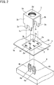
- FIG. 2 is an enlarged perspective view of a module - terminal block connection structure (also a connection method) of a first embodiment focusing on one arbitrary terminal block 3 in FIG. 1 .
- the terminal block 3 is obtained by forming a conductive material into a three-dimensional shape.
- the terminal block 3 includes a top plate portion 3a of the upper surface of the drawing, a pair of side portions 3b, and leg portions 3c formed at a lower end of each side portion 3b.
- a female screw 3d is formed at the top plate portion 3a, for example, by burring.
- a male screw and the like of the terminal block 3 are not illustrated in FIG. 2 .
- a copper pattern 2 which is a "conductive portion" is formed at a predetermined position on the front surface 1a of the printed wiring board 1.
- a similar copper pattern 2 is also formed on the rear surface 1 b and the copper patterns 2 on the front and rear surfaces are connected via through-holes 2a and 2b.
- the four through-holes 2a are located at positions corresponding to the leg portions 3c of the terminal block 3, and the leg portions 3c can pass therethrough.
- the leg portions 3c are fixed to the printed wiring board 1 by soldering.
- the terminal block 3 is electrically connected to the copper pattern 2 and is mechanically fixed.
- the lead pin 4a protruding upward in the drawing from the power module 4 is a press-fit type pin.
- press-fit type pins There are various types of press-fit type pins, but here, for example, there is one pair of U shapes as illustrated in the drawing (however, only one U-shaped pin can be also used in the copper pattern 2).
- the lead pin 4a has a press-fitting portion 4b that bulges outward slightly in the middle in the height direction. When the press-fit portion 4b is pressed into the through-hole 2b to be compressed and deformed, the lead pin 4a can be pressed into the printed wiring board 1. Accordingly, the lead pin 4a is electrically connected to the copper pattern 2.
- the lead pin 4a is within the region of the terminal block 3 when the terminal block 3 is viewed from just above the terminal block 3. In other words, the lead pin 4a exists in a space between the pair of side portions 3b below the top plate portion 3a, that is, an "under-crotch-area" of the terminal block 3.
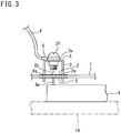
- FIG. 3 is a view illustrating a state where electric wires are further connected to the module - terminal block connection structure assembled in the manner illustrated in FIG. 2 .
- An electric wire 6 having a crimp terminal 5 attached to its tip is connected to the terminal block 3.
- the crimp terminal 5 is fixed to the terminal block 3 by screwing the male screw 3f via a washer 3e.
- the lead pin 4a press-inserted into the through-hole 2b is electrically connected to the terminal block 3 via the copper patterns 2 on both surfaces of the printed wiring board 1.
- the power module 4 and the terminal block 3 can be electrically connected to each other in such a manner that the terminal block 3 and the device to be mounted are mounted on one surface (front surface 1a) of the printed wiring board 1 and thereafter the lead pin 4a is press-inserted from the other surface (rear surface 1b).
- the lead pin 4a does not need soldering.
- the press-fit type lead pin 4a can be connected if only holes are formed even in a narrow place, connection can be realized in the vicinity of the terminal block 3, and the copper pattern 2 (conductive portion) can be suppressed from being heated when a large current flows thereto.
- the terminal block 3 contributes to heat dissipation. Therefore, it is possible to provide a module - terminal block connection structure which easily copes with the heat of the printed wiring board 1 and is suitable for manufacturing without using a terminal block having an extremely special shape.
- the lead pin 4a exists within the region of the terminal block 3 when the printed wiring board 1 is viewed from above, since the lead pin 4a is inserted from the rear side of the terminal block 3 and the pin tip comes out to an under-crotch-area of the terminal block 3, a distance from the lead pin 4a to the terminal block 3 becomes short and thus the conduction of heat to the terminal block 3 and the dissipation of heat from the terminal block 3 via the copper pattern 2 can be promoted. Moreover, since the electric resistance becomes smaller as the distance becomes shorter, the voltage drop can be suppressed.
- the copper patterns 2 provided on both surfaces (1a, 1b) of the printed wiring board 1 are connected to each other via the through-holes 2a and 2b. Therefore, by using the copper patterns 2 of both surfaces, current flows and the heat can be dispersed to escape therefrom.
- the position of the lead pin 4a be within the region of the terminal block 3 when viewed from above, it is possible to prevent the copper pattern 2 from becoming longer if the lead pin is in the vicinity of the terminal block 3 instead of the position within the region. Thus, it is possible to suppress the generation of heat in the copper pattern 2 and to promote the dissipation of heat from the terminal block 3.
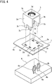
- FIG. 4 is a perspective view of a module - terminal block connection structure in which the lead pins 4a are disposed in the vicinity of the terminal block 3 instead of the "under-crotch-area" thereof.
- the difference from FIG. 2 is that the through-hole 2b is formed in the vicinity of the outer side when the terminal block 3 is viewed above, and the other configuration is the same.
- an increase in length of the copper pattern 2 can be suppressed similarly to FIG. 2 , it is possible to suppress the generation of heat in the copper pattern 2 and promote the dissipation of heat from the terminal block 3.
- the direction of each of the lead pin 4a and the through-hole 2b is merely an example.
- FIG. 5 is a diagram illustrating an outline (in which a control circuit is omitted) of the main circuit of the power module 4.
- the power module 4 includes a rectifier circuit 41 at a front stage and an inverter circuit 42 at a rear stage. If the terminal block 3 is used, the terminal block is used as an input terminal to the rectifier circuit 41 and an output terminal to the motor 15. In addition, since a reactor 16 is generally placed outside the power module 4, the terminal block 3 can also be used for connecting the reactor 16 and the power module 4. Then, the press-fit type lead pin 4a can be used in combination with the terminal block 3 as a set.
- FIG. 6 is an enlarged perspective view of a module - terminal block connection structure (also a connection method) of a third embodiment.
- the terminal block 3 is obtained by forming a conductive material into a three-dimensional shape.
- the terminal block 3 includes the top plate portion 3a of the upper surface of the drawing, the pair of side portions 3b, and the leg portions 3c formed at a lower end of each side portion 3b and further includes a bottom portion 3g fixed to be bridged between the pair of side portions 3b.
- This embodiment is the same as the first embodiment except for the bottom portion 3g.
- the bottom portion 3g has a hole 3h for press-inserting the lead pin 4a thereinto.
- the bottom portion 3g serves as a part of the terminal block 3 and also serves as a conductive portion which is electrically connected to the lead pin 4a of the power module 4.
- a through-hole 2a is formed at a predetermined place corresponding to the leg portion 3c of the terminal block 3 and the copper pattern 2 is formed to surround the through-hole.
- the copper pattern 2 is formed on both surfaces of the printed wiring board 1.
- a hole 2c for inserting the lead pin 4a therethrough is formed in the printed wiring board 1 to be located between the pair of copper patterns 2.
- the hole 2c is a simple penetration hole and is not a through-hole with copper pattern.
- the leg portion 3c of the terminal block 3 is fixed to the printed wiring board 1 by soldering.
- the lead pin 4a which protrudes upward from the power module 4 is a press-fit type pin.
- a press-fit type pin having a shape similar to that of the first embodiment is used.
- the lead pin 4a exists within the region of the terminal block 3 when the terminal block 3 is viewed from just above the terminal block 3.
- the lead pin 4a can be directly connected to the terminal block 3
- the electric resistance of the whole electric circuit becomes smaller than those of the first and second embodiments and thus the generation of heat of the whole electric circuit can be suppressed. Further, it is possible to suppress the heat of the power module 4 from being directly conducted from the lead pin 4a to the printed wiring board 1.
- a terminal block 30 having a partition in an insulation member illustrated in FIG. 7 can be used.
- connection structure connection method between the power module 4 and the terminal block 3
- the invention is not limited to the power module.
- the same connection structure can be also applied to other modules (obtained by packaging a circuit and including a lead pin) which need to be connected to the terminal block provided on the printed wiring board.
Landscapes
- Engineering & Computer Science (AREA)
- Microelectronics & Electronic Packaging (AREA)
- Coupling Device And Connection With Printed Circuit (AREA)
- Connections Arranged To Contact A Plurality Of Conductors (AREA)
Abstract
Description
- The present invention relates to a connection structure and a connection method between a lead pin of a module, which is formed by packaging a predetermined electric circuit, and an external terminal block.
- For example, an inverter in an air conditioner is formed into a power module in which necessary peripheral circuits are packaged, and this power module is attached to a printed wiring board. At that time, lead pins coming out of the power module are soldered to a copper pattern of the printed wiring board. Lead pins of a main circuit through which a current supplied to a motor flows are connected to a terminal block via the copper pattern on the board. A crimp terminal of the electric wire can be connected to the terminal block by screw clamp. The terminal block and other devices are disposed on, for example, a front surface of the printed wiring board, and the power module is disposed on a rear surface. The arrangement on the front and rear surfaces is convenient for attaching a radiation fin to the power module (for example, see Patent Literature 1 (
FIG. 3 )). - Patent Literature 1:
JP 2009-289734 A - Incidentally, since an increase in capacity of the inverter causes an increase in current amount, it is necessary to widen, for example, the width of the copper pattern on the printed circuit board. However, if the width is widened, it becomes difficult to design a pattern considering an insulation distance and generation of heat on a printed wiring board which needs to be compactly formed. In particular, it is difficult to design a pattern when densely arranging terminal blocks of three phases (six in total) in one row. It is also possible to shift the terminal blocks one by one without arranging them in one row, but since the electric resistance increases correspondingly as the copper pattern becomes longer, an extra heat countermeasure is also required. On the other hand, it is possible to thicken the thickness without changing the width of the copper pattern or use a copper bar of the same thickness, but this countermeasure is expensive and not practical.
Patent Literature 1 proposes a technique of directly connecting a power module to a terminal block by using a terminal block having an extremely special shape. However, in this case, a general-purpose inexpensive terminal block cannot be used. In addition, it is necessary to perform a step of soldering the two components on the opposite side with the printed wiring board interposed therebetween separately from a step of soldering the other devices. As a result, this technique is inconvenient in the manufacturing process. - In view of the above-described problems of the related art, an object of the invention is to provide a module - terminal block connection structure and a module - terminal block connection method which easily cope with heat of a printed wiring board and are suitable for manufacturing without using a terminal block having an extremely special shape.
-
- (1) The invention provides a module - terminal block connection structure including: a printed wiring board; a terminal block which is disposed on one surface (1a) of the printed wiring board and is formed into a three-dimensional shape by a conductive material, the terminal block being fixed to the printed wiring board; a module which is disposed on the other surface of the printed wiring board and includes an electric circuit and a press-fit type lead pin used as a circuit terminal; and a conductive portion which is electrically connected to the terminal block and includes a hole for press-inserting the lead pin thereinto, the conductive portion being electrically connected to the module while the lead pin is press-inserted into the hole.
In such a module - terminal block connection structure, the module and the terminal block can be electrically connected to each other in such a manner that the terminal block and the device to be mounted are mounted on one surface of the printed wiring board and thereafter the lead pin is press-inserted from the other surface. Thus, the lead pin does not need soldering. Also, since the press-fit type lead pin can be connected if only holes are formed even in a narrow place, connection can be realized in the vicinity of the terminal block, and the conductive portion can be suppressed from being heated when a large current flows. Moreover, the terminal block contributes to heat dissipation. Thus, it is possible to provide a module - terminal block connection structure which easily copes with heat of a printed wiring board and is suitable for manufacturing without using a terminal block having an extremely special shape. - (2) Further, in the module - terminal block connection structure of (1), the lead pin may exist within a region of the terminal block when the printed wiring board is viewed from above.
In this case, since the lead pin is inserted from the rear side of the terminal block and the pin tip comes out to an "under-crotch-area" of the terminal block, a distance from the lead pin to the terminal block becomes short and thus the conduction of heat to the terminal block and the dissipation of heat from the terminal block can be promoted. Further, since the electric resistance becomes smaller as the distance becomes shorter, the voltage drop can be suppressed. - (3) Further, in the module - terminal block connection structure of (1) or (2), the conductive portion may be a copper pattern formed on both surfaces of the printed wiring board and the hole may be a through-hole.
In this case, by using the copper patterns of both surfaces, current flows and the heat can be dispersed to escape therefrom. - (4) Further, in the module - terminal block connection structure of (2), the terminal block may include a top plate portion to which the external wire is attached, a pair of side portions, a leg portion which is formed at a lower end of each side portion, and a bottom portion which is provided to be bridged between the pair of side portions, and also, the bottom portion may be the conductive portion.
In this case, since the lead pin can be directly connected to the terminal block, the electric resistance of the whole electric circuit is further reduced and thus the generation of heat of the whole electric circuit can be suppressed. Further, it is possible to suppress the heat of the module from being directly conducted from the lead pin to the printed wiring board. - (5) Further, in the module - terminal block connection structure of any one of (1) to (4), the module may be a power module which controls a current supplied to a motor by switching.
A radiation fin or the like is generally attached to the power module since heat is generated due to switching loss caused when a current which is larger than that of the control circuit flows to the power module. According to the module - terminal block connection structure, since the dissipation of heat from the terminal block can be also promoted, the heat dissipation effect of the power module is excellent. - (6) Meanwhile, the invention provides a module - terminal block connection method of electrically connecting a lead pin corresponding to a circuit terminal of a module of an electric circuit to a terminal block used for connection with an external wire, the module - terminal block connection method including: (i) mounting the terminal block and a conductive portion electrically connected to the terminal block and including a hole for press-inserting the lead pin thereinto onto a printed wiring board; and (ii) disposing the module on the side opposite to the terminal block in the printed wiring board and press-inserting the press-fit type lead pin into the hole so that the module is electrically connected to the terminal block.
- According to such a module - terminal block connection method, the module and the terminal block can be electrically connected to each other in such a manner that the terminal block and the device to be mounted are mounted on one surface of the printed wiring board and thereafter the lead pin is press-inserted from the other surface. Thus, the lead pin does not need soldering. Also, since the press-fit type lead pin can be connected if only holes are formed even in a narrow place, connection can be realized in the vicinity of the terminal block, and the conductive portion can be suppressed from being heated when a large current flows. Moreover, the terminal block contributes to heat dissipation. Thus, it is possible to provide a module - terminal block connection method which easily copes with heat of a printed wiring board and is suitable for manufacturing without using a terminal block having an extremely special shape.
- According to the invention, it is possible to provide a module - terminal block connection structure and a module - terminal block connection method which easily cope with heat of a printed wiring board and are suitable for manufacturing without using a terminal block having an extremely special shape.
-
-
FIG. 1 is a perspective view illustrating an outline of a printed wiring board unit mounted to, for example, an air conditioner; -
FIG. 2 is an enlarged perspective view of a module - terminal block connection structure (also a connection method) of a first embodiment focusing on one arbitrary terminal block inFIG. 1 ; -
FIG. 3 is a view illustrating a state where an electric wire is further connected to the module - terminal block connection structure assembled in the manner illustrated inFIG. 2 ; -
FIG. 4 is a perspective view of a module - terminal block connection structure in which lead pins are disposed in the vicinity of the terminal block instead of an "under-crotch-area" thereof; -
FIG. 5 is a diagram illustrating an outline (in which a control circuit is omitted) of a main circuit of a power module; -
FIG. 6 is an enlarged perspective view of a module - terminal block connection structure (also a connection method) of a third embodiment; and -
FIG. 7 is a perspective view illustrating a terminal block having a partition of an insulation member. - Hereinafter, embodiments of the invention will be described with reference to the drawings.
-
FIG. 1 is a perspective view illustrating an outline of a printedwiring board unit 100 mounted to, for example, an air conditioner. For example, a power supply circuit 11, aCPU 12, acapacitor 13, other circuit components, and connection members such as aterminal block 3 and a connector (not illustrated) are mounted on afront surface 1a of a printedwiring board 1. Theterminal block 3 is used for a main circuit to which a large current, that cannot forces to flow in a connector, flows. The main circuit is a circuit that supplies a current to, for example, a motor (not illustrated) that drives a compressor in the air conditioner. Theterminal blocks 3 are arranged with ensuring a necessary insulation distance therebetween. - A
power module 4 is provided on arear surface 1 b of the printedwiring board 1. Aradiation fin 14 is attached to thepower module 4 that generates heat due to switching loss or the like. Thepower module 4 is formed such that a motor drive circuit including an inverter is packaged with a resin, and leadpins 4a necessary for connection with the outside are projected therefrom. Since the lead pins 4a are used for the main circuit and control, more lead pins actually exist. However, only sixlead pins 4a corresponding to input terminals (three phases: R, S, T) and output terminals (three phases: u, v, w) for the main circuit are briefly depicted herein. - Each component to be mounted on the
front surface 1a of the printedwiring board 1 is designed such that a tip of an electrode or an attachment leg slightly protrudes toward therear surface 1b and is soldered to therear surface 1b by, for example, a flow method using a solder bath so as to be securely mounted on the printedwiring board 1. Further, a hole (to be described later in detail) for inserting thelead pin 4a thereinto is formed on the inner lower side of theterminal block 3 and, when thelead pin 4a is pressed into this hole, theterminal block 3 and thelead pin 4a can be electrically and mechanically connected to each other. For example, a crimp terminal at a tip of an electric wire can be attached to theterminal block 3 while being interposed between theterminal block 3 and amale screw 3f (FIG. 3 ). -
FIG. 2 is an enlarged perspective view of a module - terminal block connection structure (also a connection method) of a first embodiment focusing on onearbitrary terminal block 3 inFIG. 1 . As illustrated in the drawing, theterminal block 3 is obtained by forming a conductive material into a three-dimensional shape. Theterminal block 3 includes atop plate portion 3a of the upper surface of the drawing, a pair ofside portions 3b, andleg portions 3c formed at a lower end of eachside portion 3b. Afemale screw 3d is formed at thetop plate portion 3a, for example, by burring. A male screw and the like of theterminal block 3 are not illustrated inFIG. 2 . In fact, there is roundness (curvature) at a bent portion from thetop plate portion 3a to theside portion 3b, but the bent portion is simply depicted herein. - A
copper pattern 2 which is a "conductive portion" is formed at a predetermined position on thefront surface 1a of the printedwiring board 1. Asimilar copper pattern 2 is also formed on therear surface 1 b and thecopper patterns 2 on the front and rear surfaces are connected via through-holes holes 2a are located at positions corresponding to theleg portions 3c of theterminal block 3, and theleg portions 3c can pass therethrough. Theleg portions 3c are fixed to the printedwiring board 1 by soldering. As a result, theterminal block 3 is electrically connected to thecopper pattern 2 and is mechanically fixed. - The
lead pin 4a protruding upward in the drawing from thepower module 4 is a press-fit type pin. There are various types of press-fit type pins, but here, for example, there is one pair of U shapes as illustrated in the drawing (however, only one U-shaped pin can be also used in the copper pattern 2). Thelead pin 4a has a press-fittingportion 4b that bulges outward slightly in the middle in the height direction. When the press-fit portion 4b is pressed into the through-hole 2b to be compressed and deformed, thelead pin 4a can be pressed into the printedwiring board 1. Accordingly, thelead pin 4a is electrically connected to thecopper pattern 2. - In the module - terminal block connection structure assembled in the manner illustrated in
FIG. 2 , thelead pin 4a is within the region of theterminal block 3 when theterminal block 3 is viewed from just above theterminal block 3. In other words, thelead pin 4a exists in a space between the pair ofside portions 3b below thetop plate portion 3a, that is, an "under-crotch-area" of theterminal block 3. -
FIG. 3 is a view illustrating a state where electric wires are further connected to the module - terminal block connection structure assembled in the manner illustrated inFIG. 2 . An electric wire 6 having acrimp terminal 5 attached to its tip is connected to theterminal block 3. Thecrimp terminal 5 is fixed to theterminal block 3 by screwing themale screw 3f via awasher 3e. - The
lead pin 4a press-inserted into the through-hole 2b is electrically connected to theterminal block 3 via thecopper patterns 2 on both surfaces of the printedwiring board 1. - According to the above-described module - terminal block connection structure (connection method), the
power module 4 and theterminal block 3 can be electrically connected to each other in such a manner that theterminal block 3 and the device to be mounted are mounted on one surface (front surface 1a) of the printedwiring board 1 and thereafter thelead pin 4a is press-inserted from the other surface (rear surface 1b). Thus, thelead pin 4a does not need soldering. Also, since the press-fittype lead pin 4a can be connected if only holes are formed even in a narrow place, connection can be realized in the vicinity of theterminal block 3, and the copper pattern 2 (conductive portion) can be suppressed from being heated when a large current flows thereto. Moreover, theterminal block 3 contributes to heat dissipation. Therefore, it is possible to provide a module - terminal block connection structure which easily copes with the heat of the printedwiring board 1 and is suitable for manufacturing without using a terminal block having an extremely special shape. - Further, in the connection structure in which the
lead pin 4a exists within the region of theterminal block 3 when the printedwiring board 1 is viewed from above, since thelead pin 4a is inserted from the rear side of theterminal block 3 and the pin tip comes out to an under-crotch-area of theterminal block 3, a distance from thelead pin 4a to theterminal block 3 becomes short and thus the conduction of heat to theterminal block 3 and the dissipation of heat from theterminal block 3 via thecopper pattern 2 can be promoted. Moreover, since the electric resistance becomes smaller as the distance becomes shorter, the voltage drop can be suppressed. Here, thecopper patterns 2 provided on both surfaces (1a, 1b) of the printedwiring board 1 are connected to each other via the through-holes copper patterns 2 of both surfaces, current flows and the heat can be dispersed to escape therefrom. - Further, according to such a module - terminal block connection structure, since the dissipation of heat from the
terminal block 3 can be promoted, the heat dissipation effect of thepower module 4 is excellent. - Although it is desirable that the position of the
lead pin 4a be within the region of theterminal block 3 when viewed from above, it is possible to prevent thecopper pattern 2 from becoming longer if the lead pin is in the vicinity of theterminal block 3 instead of the position within the region. Thus, it is possible to suppress the generation of heat in thecopper pattern 2 and to promote the dissipation of heat from theterminal block 3. - For example,
FIG. 4 is a perspective view of a module - terminal block connection structure in which the lead pins 4a are disposed in the vicinity of theterminal block 3 instead of the "under-crotch-area" thereof. The difference fromFIG. 2 is that the through-hole 2b is formed in the vicinity of the outer side when theterminal block 3 is viewed above, and the other configuration is the same. Also in this case, since an increase in length of thecopper pattern 2 can be suppressed similarly toFIG. 2 , it is possible to suppress the generation of heat in thecopper pattern 2 and promote the dissipation of heat from theterminal block 3. The direction of each of thelead pin 4a and the through-hole 2b is merely an example. -
FIG. 5 is a diagram illustrating an outline (in which a control circuit is omitted) of the main circuit of thepower module 4. Thepower module 4 includes arectifier circuit 41 at a front stage and aninverter circuit 42 at a rear stage. If theterminal block 3 is used, the terminal block is used as an input terminal to therectifier circuit 41 and an output terminal to themotor 15. In addition, since areactor 16 is generally placed outside thepower module 4, theterminal block 3 can also be used for connecting thereactor 16 and thepower module 4. Then, the press-fittype lead pin 4a can be used in combination with theterminal block 3 as a set. -
FIG. 6 is an enlarged perspective view of a module - terminal block connection structure (also a connection method) of a third embodiment. As illustrated in the drawing, theterminal block 3 is obtained by forming a conductive material into a three-dimensional shape. Theterminal block 3 includes thetop plate portion 3a of the upper surface of the drawing, the pair ofside portions 3b, and theleg portions 3c formed at a lower end of eachside portion 3b and further includes abottom portion 3g fixed to be bridged between the pair ofside portions 3b. This embodiment is the same as the first embodiment except for thebottom portion 3g. Thebottom portion 3g has ahole 3h for press-inserting thelead pin 4a thereinto. Thebottom portion 3g serves as a part of theterminal block 3 and also serves as a conductive portion which is electrically connected to thelead pin 4a of thepower module 4. - In the printed
wiring board 1, a through-hole 2a is formed at a predetermined place corresponding to theleg portion 3c of theterminal block 3 and thecopper pattern 2 is formed to surround the through-hole. Thecopper pattern 2 is formed on both surfaces of the printedwiring board 1. Further, ahole 2c for inserting thelead pin 4a therethrough is formed in the printedwiring board 1 to be located between the pair ofcopper patterns 2. Thehole 2c is a simple penetration hole and is not a through-hole with copper pattern. Theleg portion 3c of theterminal block 3 is fixed to the printedwiring board 1 by soldering. - The
lead pin 4a which protrudes upward from thepower module 4 is a press-fit type pin. Although there are various press-fit type pins, a press-fit type pin having a shape similar to that of the first embodiment is used. When the press-fittingportion 4b of thelead pin 4a is pressed into thehole 3h of thebottom portion 3g of theterminal block 3 to be compressed and deformed, thelead pin 4a is electrically connected to thecopper pattern 2. - Even in the module - terminal block connection structure assembled in the manner of
FIG. 6 , thelead pin 4a exists within the region of theterminal block 3 when theterminal block 3 is viewed from just above theterminal block 3. - In the case of the module - terminal block connection structure of
FIG. 6 , since thelead pin 4a can be directly connected to theterminal block 3, the electric resistance of the whole electric circuit becomes smaller than those of the first and second embodiments and thus the generation of heat of the whole electric circuit can be suppressed. Further, it is possible to suppress the heat of thepower module 4 from being directly conducted from thelead pin 4a to the printedwiring board 1. - <<Others>>
- Further, for example, when an insulation distance between the parallel terminal blocks 3 of
FIG. 1 cannot be ensured, a terminal block 30 having a partition in an insulation member illustrated inFIG. 7 can be used. - Furthermore, in the above-described embodiments, a connection structure (connection method) between the
power module 4 and theterminal block 3 has been described, but the invention is not limited to the power module. For example, the same connection structure can be also applied to other modules (obtained by packaging a circuit and including a lead pin) which need to be connected to the terminal block provided on the printed wiring board. -
- 1: printed wiring board
- 1a: front surface
- 1b: rear surface
- 2: copper pattern
- 2a, 2b: through-hole
- 2c: hole
- 3: terminal block
- 3a: top plate portion
- 3b: side portion
- 3c: leg portion
- 3d: female screw
- 3e: washer
- 3f: male screw
- 3g: bottom portion
- 3h: hole
- 4: power module
- 4a: lead pin
- 4b: press-fitting portion
- 5: crimp terminal
- 6: electric wire
- 11: power supply circuit
- 12: CPU
- 13: capacitor
- 14: radiation fin
- 15: motor
- 16: reactor
- 30: terminal block
- 41: rectifier circuit
- 42: inverter circuit
- 100: printed wiring board unit
Claims (6)
- A module - terminal block connection structure comprising:a printed wiring board (1);a terminal block (3) which is disposed on one surface (1a) of the printed wiring board (1) and is formed into a three-dimensional shape by a conductive material, the terminal block (3) being fixed to the printed wiring board (1);a module (4) which is disposed on the other surface (1b) of the printed wiring board (1) and includes an electric circuit and a press-fit type lead pin (4a) used as a circuit terminal; anda conductive portion (2, 3g) which is electrically connected to the terminal block (3) and includes a hole (2b, 3h) for press-inserting the lead pin (4a) thereinto, the conductive portion (2, 3g) being electrically connected to the module (4) while the lead pin (4a) is press-inserted into the hole (2b, 3h).
- The module - terminal block connection structure according to claim 1,
wherein the lead pin (4a) exists within a region of the terminal block (3) when the printed wiring board (1) is viewed from above. - The module - terminal block connection structure according to claim 1 or 2,
wherein the conductive portion (2) is a copper pattern formed on both surfaces (1a, 1b) of the printed wiring board (1) and the hole (2b) is a through-hole. - The module - terminal block connection structure according to claim 2,
wherein the terminal block (3) includes a top plate portion (3a) to which the external wire is attached, a pair of side portions (3b), a leg portion (3c) which is formed at a lower end of each side portion (3b), and a bottom portion (3c) which is provided to be bridged between the pair of side portions, and also, the bottom portion (3c) is the conductive portion. - The module - terminal block connection structure according to any one of claims 1 to 4,
wherein the module is a power module which controls a current supplied to a motor by switching. - A module - terminal block connection method of electrically connecting a lead pin (4a) corresponding to a circuit terminal of a module (4) of an electric circuit to a terminal block (3) used for connection with an external wire, the module - terminal block connection method comprising:mounting the terminal block (3) and a conductive portion (2, 3g) electrically connected to the terminal block and including a hole (2b, 3h) for press-inserting the lead pin (4a) thereinto onto a printed wiring board (1); anddisposing the module (4) on the side opposite to the terminal block (3) in the printed wiring board (1) and press-inserting the press-fit type lead pin (4a) into the hole (2b, 3h) so that the module (4) is electrically connected to the terminal block (3).
Applications Claiming Priority (2)
| Application Number | Priority Date | Filing Date | Title |
|---|---|---|---|
| JP2014255381A JP6488688B2 (en) | 2014-12-17 | 2014-12-17 | Module-terminal block connection structure and connection method |
| PCT/JP2015/081025 WO2016098475A1 (en) | 2014-12-17 | 2015-11-04 | Module-terminal block connection structure and connection method |
Publications (2)
| Publication Number | Publication Date |
|---|---|
| EP3236533A1 true EP3236533A1 (en) | 2017-10-25 |
| EP3236533A4 EP3236533A4 (en) | 2018-06-13 |
Family
ID=56126374
Family Applications (1)
| Application Number | Title | Priority Date | Filing Date |
|---|---|---|---|
| EP15869683.1A Withdrawn EP3236533A4 (en) | 2014-12-17 | 2015-11-04 | Module-terminal block connection structure and connection method |
Country Status (6)
| Country | Link |
|---|---|
| US (1) | US10038256B2 (en) |
| EP (1) | EP3236533A4 (en) |
| JP (1) | JP6488688B2 (en) |
| CN (1) | CN107112654B (en) |
| AU (1) | AU2015365104B2 (en) |
| WO (1) | WO2016098475A1 (en) |
Cited By (1)
| Publication number | Priority date | Publication date | Assignee | Title |
|---|---|---|---|---|
| WO2022189046A1 (en) * | 2021-03-09 | 2022-09-15 | Würth Elektronik Ics Gmbh & Co. Kg | Connector device for fastening electronic components on a circuit board |
Families Citing this family (7)
| Publication number | Priority date | Publication date | Assignee | Title |
|---|---|---|---|---|
| JP2018081863A (en) * | 2016-11-18 | 2018-05-24 | 株式会社ノーリツ | Electrical equipment |
| DE102018118976A1 (en) * | 2018-08-03 | 2020-02-06 | Würth Elektronik Ics Gmbh & Co. Kg | Device for the transmission of electrical signals or of electrical current, an electrical assembly and a kit |
| WO2020157563A2 (en) * | 2019-01-29 | 2020-08-06 | Appleton Grp, Llc | A heat-absorbing-and-dissipating jacket for a terminal of an electrical device |
| DE102021201454A1 (en) * | 2021-02-16 | 2022-08-18 | Robert Bosch Gesellschaft mit beschränkter Haftung | Connecting device, in particular for connecting an electrical and/or electronic component to a conductor substrate |
| JP7285892B2 (en) * | 2021-09-15 | 2023-06-02 | 新電元工業株式会社 | Terminal assembly structure and electronic device |
| JP7414878B2 (en) * | 2022-04-04 | 2024-01-16 | 三菱電機株式会社 | power converter |
| TWM644289U (en) * | 2023-05-05 | 2023-07-21 | 健和興端子股份有限公司 | Connecting terminal fixing structure |
Family Cites Families (30)
| Publication number | Priority date | Publication date | Assignee | Title |
|---|---|---|---|---|
| US1177346A (en) * | 1913-02-07 | 1916-03-28 | Westinghouse Electric & Mfg Co | Coil-terminal. |
| US2854552A (en) * | 1955-12-27 | 1958-09-30 | Illinois Tool Works | Switch means for printed circuits |
| US3384853A (en) * | 1965-04-16 | 1968-05-21 | Gen Motors Corp | Printed circuit terminal nut |
| US3325774A (en) * | 1965-05-07 | 1967-06-13 | Gen Electric | Terminal board design |
| US3624588A (en) * | 1970-02-26 | 1971-11-30 | Farmer Elecric Products Co Inc | Screw terminal and conductive devices incorporating such terminals |
| GB1493220A (en) * | 1976-10-12 | 1977-11-30 | Pye Ltd | Screw or nut and a washer intended to be held captive thereon |
| JPS5825051U (en) * | 1981-08-11 | 1983-02-17 | 富士通テン株式会社 | lead pin |
| US4630882A (en) * | 1985-01-18 | 1986-12-23 | Reed Devices, Inc. | Low profile screw terminal block with split plastic barrel |
| US4680672A (en) * | 1985-11-08 | 1987-07-14 | Siemens-Allis | Molded case circuit breaker with front accessible control panel |
| US4732568A (en) * | 1986-03-17 | 1988-03-22 | Virginia Plastics Company | Electrical connector with integral ground strap for shielded cable |
| US4792880A (en) * | 1986-10-03 | 1988-12-20 | Westinghouse Electric Corp. | Terminal module |
| US4738638A (en) * | 1986-10-28 | 1988-04-19 | Virginia Plastics Company | Electrical connector with improved integral ground strap for shielded cable |
| JPH02137052U (en) * | 1989-04-14 | 1990-11-15 | ||
| JPH06302932A (en) * | 1993-04-09 | 1994-10-28 | Toyo Electric Mfg Co Ltd | Printed wiring board |
| US6242993B1 (en) * | 1995-03-13 | 2001-06-05 | Square D Company | Apparatus for use in arcing fault detection systems |
| US5741161A (en) * | 1996-01-04 | 1998-04-21 | Pcd Inc. | Electrical connection system with discrete wire interconnections |
| JP2000251977A (en) * | 1999-02-26 | 2000-09-14 | Fujitsu Ltd | Power supply terminal |
| US6380846B1 (en) * | 1999-08-13 | 2002-04-30 | Pittway Corporation | Pull station |
| US6319018B1 (en) * | 2000-02-29 | 2001-11-20 | Avaya Technology Corp. | Circuit board electrical and physical connection system and method |
| US6302709B1 (en) * | 2000-06-05 | 2001-10-16 | Power-One, Inc. | Multiple function high current interconnect with integrated bus bar |
| JP4425730B2 (en) * | 2003-07-09 | 2010-03-03 | 株式会社オートネットワーク技術研究所 | Connector terminal manufacturing method |
| JP2005318693A (en) * | 2004-04-27 | 2005-11-10 | Auto Network Gijutsu Kenkyusho:Kk | Connection structure and connection method between press-fit terminal and bus bar |
| JP4410242B2 (en) * | 2006-12-27 | 2010-02-03 | 三菱電機株式会社 | Electronic control device and manufacturing method thereof |
| TWI358175B (en) * | 2008-01-16 | 2012-02-11 | Delta Electronics Inc | Ground terminal |
| JP4450104B2 (en) | 2008-04-30 | 2010-04-14 | ダイキン工業株式会社 | Connection member mounting structure and refrigeration system |
| JP2015038896A (en) * | 2008-04-30 | 2015-02-26 | ダイキン工業株式会社 | Printed wiring board unit and freezer |
| DE102009042385A1 (en) * | 2009-09-21 | 2011-04-14 | Würth Elektronik Ics Gmbh & Co. Kg | Multi Fork press-in pin |
| JP4816788B2 (en) * | 2009-10-29 | 2011-11-16 | ダイキン工業株式会社 | Wiring board unit |
| DE112012002122B4 (en) * | 2011-05-17 | 2020-11-26 | Interplex Industries, Inc. | Inter-plate connection system with deformation avoidance of flexible flexible pins |
| CN104919657B (en) | 2013-01-14 | 2019-05-10 | 威世通用半导体公司 | Voltage distribution pins for semiconductor modules |
-
2014
- 2014-12-17 JP JP2014255381A patent/JP6488688B2/en not_active Expired - Fee Related
-
2015
- 2015-11-04 CN CN201580068870.5A patent/CN107112654B/en not_active Expired - Fee Related
- 2015-11-04 AU AU2015365104A patent/AU2015365104B2/en not_active Ceased
- 2015-11-04 EP EP15869683.1A patent/EP3236533A4/en not_active Withdrawn
- 2015-11-04 WO PCT/JP2015/081025 patent/WO2016098475A1/en not_active Ceased
- 2015-11-04 US US15/523,511 patent/US10038256B2/en not_active Expired - Fee Related
Cited By (1)
| Publication number | Priority date | Publication date | Assignee | Title |
|---|---|---|---|---|
| WO2022189046A1 (en) * | 2021-03-09 | 2022-09-15 | Würth Elektronik Ics Gmbh & Co. Kg | Connector device for fastening electronic components on a circuit board |
Also Published As
| Publication number | Publication date |
|---|---|
| JP6488688B2 (en) | 2019-03-27 |
| EP3236533A4 (en) | 2018-06-13 |
| AU2015365104A1 (en) | 2017-05-25 |
| AU2015365104B2 (en) | 2018-08-30 |
| CN107112654B (en) | 2019-11-22 |
| WO2016098475A1 (en) | 2016-06-23 |
| JP2016115623A (en) | 2016-06-23 |
| CN107112654A (en) | 2017-08-29 |
| US10038256B2 (en) | 2018-07-31 |
| US20170324173A1 (en) | 2017-11-09 |
Similar Documents
| Publication | Publication Date | Title |
|---|---|---|
| US10038256B2 (en) | Module-terminal block connection structure and connection method | |
| US20140198470A1 (en) | Printed circuit board stack | |
| CN111344823A (en) | DC link capacitor modules, power electronics modules and power electronics | |
| US20120214321A1 (en) | Circuit board unit | |
| JP6033164B2 (en) | Terminal, electronic control device | |
| JP2010186663A (en) | Low-height type surface mounting fast-on tab terminal | |
| US9942988B2 (en) | Circuit board and power supply apparatus | |
| JP6443265B2 (en) | Mounting board | |
| US9337595B1 (en) | Busbar connection system | |
| CN104701112A (en) | Terminal, circuit board module comprising same and method for manufacturing same | |
| JP4234687B2 (en) | Electrical junction box for automobiles | |
| JP5516076B2 (en) | Circuit structure and electrical junction box | |
| JP5811884B2 (en) | PCB terminal fittings | |
| JP3624151B2 (en) | Electrical component connection structure | |
| JP2018148180A (en) | Electrical component, electrical component mounting structure, and electrical component fixing member | |
| JP2020022235A (en) | Power conversion device and bus bar | |
| JP2011125156A (en) | Circuit structure | |
| JP7627561B2 (en) | Electronics | |
| JP5926845B1 (en) | Unidirectional soldering case | |
| EP2808961A1 (en) | Bus bar | |
| KR102006853B1 (en) | Terminal Lug for supplying Power | |
| JP2016012591A (en) | Electronic circuit body and manufacturing method thereof | |
| KR20180052376A (en) | Pork terminal and vehicular junction box having the same | |
| JP5569692B2 (en) | Electrical junction box | |
| CN104303296A (en) | Circuit assembly |
Legal Events
| Date | Code | Title | Description |
|---|---|---|---|
| STAA | Information on the status of an ep patent application or granted ep patent |
Free format text: STATUS: THE INTERNATIONAL PUBLICATION HAS BEEN MADE |
|
| PUAI | Public reference made under article 153(3) epc to a published international application that has entered the european phase |
Free format text: ORIGINAL CODE: 0009012 |
|
| STAA | Information on the status of an ep patent application or granted ep patent |
Free format text: STATUS: REQUEST FOR EXAMINATION WAS MADE |
|
| 17P | Request for examination filed |
Effective date: 20170510 |
|
| AK | Designated contracting states |
Kind code of ref document: A1 Designated state(s): AL AT BE BG CH CY CZ DE DK EE ES FI FR GB GR HR HU IE IS IT LI LT LU LV MC MK MT NL NO PL PT RO RS SE SI SK SM TR |
|
| AX | Request for extension of the european patent |
Extension state: BA ME |
|
| DAV | Request for validation of the european patent (deleted) | ||
| DAX | Request for extension of the european patent (deleted) | ||
| A4 | Supplementary search report drawn up and despatched |
Effective date: 20180514 |
|
| RIC1 | Information provided on ipc code assigned before grant |
Ipc: H01R 9/22 20060101AFI20180508BHEP Ipc: H01R 12/58 20110101ALI20180508BHEP Ipc: H01R 12/51 20110101ALI20180508BHEP Ipc: H01R 4/34 20060101ALI20180508BHEP Ipc: H01R 12/70 20110101ALN20180508BHEP Ipc: H05K 1/18 20060101ALI20180508BHEP |
|
| STAA | Information on the status of an ep patent application or granted ep patent |
Free format text: STATUS: EXAMINATION IS IN PROGRESS |
|
| 17Q | First examination report despatched |
Effective date: 20200320 |
|
| GRAP | Despatch of communication of intention to grant a patent |
Free format text: ORIGINAL CODE: EPIDOSNIGR1 |
|
| STAA | Information on the status of an ep patent application or granted ep patent |
Free format text: STATUS: GRANT OF PATENT IS INTENDED |
|
| RIC1 | Information provided on ipc code assigned before grant |
Ipc: H01R 12/51 20110101ALI20201026BHEP Ipc: H01R 12/58 20110101ALI20201026BHEP Ipc: H01R 4/34 20060101ALI20201026BHEP Ipc: H01R 12/70 20110101ALN20201026BHEP Ipc: H01R 9/22 20060101AFI20201026BHEP Ipc: H05K 1/18 20060101ALI20201026BHEP |
|
| INTG | Intention to grant announced |
Effective date: 20201109 |
|
| STAA | Information on the status of an ep patent application or granted ep patent |
Free format text: STATUS: THE APPLICATION IS DEEMED TO BE WITHDRAWN |
|
| 18D | Application deemed to be withdrawn |
Effective date: 20210320 |