EP3236487A2 - Method of making semiconductor ferroelectric memory element and semiconductor ferroelectric memory transistor - Google Patents
Method of making semiconductor ferroelectric memory element and semiconductor ferroelectric memory transistor Download PDFInfo
- Publication number
- EP3236487A2 EP3236487A2 EP17167457.5A EP17167457A EP3236487A2 EP 3236487 A2 EP3236487 A2 EP 3236487A2 EP 17167457 A EP17167457 A EP 17167457A EP 3236487 A2 EP3236487 A2 EP 3236487A2
- Authority
- EP
- European Patent Office
- Prior art keywords
- ferroelectric
- annealing
- oxygen
- film
- semiconductor
- Prior art date
- Legal status (The legal status is an assumption and is not a legal conclusion. Google has not performed a legal analysis and makes no representation as to the accuracy of the status listed.)
- Granted
Links
Images






Classifications
-
- H—ELECTRICITY
- H10—SEMICONDUCTOR DEVICES; ELECTRIC SOLID-STATE DEVICES NOT OTHERWISE PROVIDED FOR
- H10D—INORGANIC ELECTRIC SEMICONDUCTOR DEVICES
- H10D64/00—Electrodes of devices having potential barriers
- H10D64/01—Manufacture or treatment
- H10D64/031—Manufacture or treatment of data-storage electrodes
- H10D64/033—Manufacture or treatment of data-storage electrodes comprising ferroelectric layers
-
- H—ELECTRICITY
- H10—SEMICONDUCTOR DEVICES; ELECTRIC SOLID-STATE DEVICES NOT OTHERWISE PROVIDED FOR
- H10B—ELECTRONIC MEMORY DEVICES
- H10B53/00—Ferroelectric RAM [FeRAM] devices comprising ferroelectric memory capacitors
-
- G—PHYSICS
- G11—INFORMATION STORAGE
- G11C—STATIC STORES
- G11C11/00—Digital stores characterised by the use of particular electric or magnetic storage elements; Storage elements therefor
- G11C11/21—Digital stores characterised by the use of particular electric or magnetic storage elements; Storage elements therefor using electric elements
- G11C11/22—Digital stores characterised by the use of particular electric or magnetic storage elements; Storage elements therefor using electric elements using ferroelectric elements
- G11C11/223—Digital stores characterised by the use of particular electric or magnetic storage elements; Storage elements therefor using electric elements using ferroelectric elements using MOS with ferroelectric gate insulating film
-
- H—ELECTRICITY
- H10—SEMICONDUCTOR DEVICES; ELECTRIC SOLID-STATE DEVICES NOT OTHERWISE PROVIDED FOR
- H10B—ELECTRONIC MEMORY DEVICES
- H10B53/00—Ferroelectric RAM [FeRAM] devices comprising ferroelectric memory capacitors
- H10B53/30—Ferroelectric RAM [FeRAM] devices comprising ferroelectric memory capacitors characterised by the memory core region
-
- H—ELECTRICITY
- H10—SEMICONDUCTOR DEVICES; ELECTRIC SOLID-STATE DEVICES NOT OTHERWISE PROVIDED FOR
- H10D—INORGANIC ELECTRIC SEMICONDUCTOR DEVICES
- H10D30/00—Field-effect transistors [FET]
- H10D30/01—Manufacture or treatment
- H10D30/021—Manufacture or treatment of FETs having insulated gates [IGFET]
- H10D30/0415—Manufacture or treatment of FETs having insulated gates [IGFET] of FETs having ferroelectric gate insulators
-
- H—ELECTRICITY
- H10—SEMICONDUCTOR DEVICES; ELECTRIC SOLID-STATE DEVICES NOT OTHERWISE PROVIDED FOR
- H10D—INORGANIC ELECTRIC SEMICONDUCTOR DEVICES
- H10D30/00—Field-effect transistors [FET]
- H10D30/60—Insulated-gate field-effect transistors [IGFET]
- H10D30/701—IGFETs having ferroelectric gate insulators, e.g. ferroelectric FETs
-
- H—ELECTRICITY
- H10—SEMICONDUCTOR DEVICES; ELECTRIC SOLID-STATE DEVICES NOT OTHERWISE PROVIDED FOR
- H10D—INORGANIC ELECTRIC SEMICONDUCTOR DEVICES
- H10D64/00—Electrodes of devices having potential barriers
- H10D64/60—Electrodes characterised by their materials
- H10D64/66—Electrodes having a conductor capacitively coupled to a semiconductor by an insulator, e.g. MIS electrodes
- H10D64/68—Electrodes having a conductor capacitively coupled to a semiconductor by an insulator, e.g. MIS electrodes characterised by the insulator, e.g. by the gate insulator
- H10D64/681—Electrodes having a conductor capacitively coupled to a semiconductor by an insulator, e.g. MIS electrodes characterised by the insulator, e.g. by the gate insulator having a compositional variation, e.g. multilayered
- H10D64/685—Electrodes having a conductor capacitively coupled to a semiconductor by an insulator, e.g. MIS electrodes characterised by the insulator, e.g. by the gate insulator having a compositional variation, e.g. multilayered being perpendicular to the channel plane
-
- H—ELECTRICITY
- H10—SEMICONDUCTOR DEVICES; ELECTRIC SOLID-STATE DEVICES NOT OTHERWISE PROVIDED FOR
- H10D—INORGANIC ELECTRIC SEMICONDUCTOR DEVICES
- H10D64/00—Electrodes of devices having potential barriers
- H10D64/60—Electrodes characterised by their materials
- H10D64/66—Electrodes having a conductor capacitively coupled to a semiconductor by an insulator, e.g. MIS electrodes
- H10D64/68—Electrodes having a conductor capacitively coupled to a semiconductor by an insulator, e.g. MIS electrodes characterised by the insulator, e.g. by the gate insulator
- H10D64/689—Electrodes having a conductor capacitively coupled to a semiconductor by an insulator, e.g. MIS electrodes characterised by the insulator, e.g. by the gate insulator having ferroelectric layers
-
- H—ELECTRICITY
- H10—SEMICONDUCTOR DEVICES; ELECTRIC SOLID-STATE DEVICES NOT OTHERWISE PROVIDED FOR
- H10P—GENERIC PROCESSES OR APPARATUS FOR THE MANUFACTURE OR TREATMENT OF DEVICES COVERED BY CLASS H10
- H10P14/00—Formation of materials, e.g. in the shape of layers or pillars
- H10P14/60—Formation of materials, e.g. in the shape of layers or pillars of insulating materials
- H10P14/63—Formation of materials, e.g. in the shape of layers or pillars of insulating materials characterised by the formation processes
- H10P14/6326—Deposition processes
- H10P14/6328—Deposition from the gas or vapour phase
- H10P14/6329—Deposition from the gas or vapour phase using physical ablation of a target, e.g. physical vapour deposition or pulsed laser deposition
-
- H—ELECTRICITY
- H10—SEMICONDUCTOR DEVICES; ELECTRIC SOLID-STATE DEVICES NOT OTHERWISE PROVIDED FOR
- H10P—GENERIC PROCESSES OR APPARATUS FOR THE MANUFACTURE OR TREATMENT OF DEVICES COVERED BY CLASS H10
- H10P14/00—Formation of materials, e.g. in the shape of layers or pillars
- H10P14/60—Formation of materials, e.g. in the shape of layers or pillars of insulating materials
- H10P14/63—Formation of materials, e.g. in the shape of layers or pillars of insulating materials characterised by the formation processes
- H10P14/6326—Deposition processes
- H10P14/6328—Deposition from the gas or vapour phase
- H10P14/6334—Deposition from the gas or vapour phase using decomposition or reaction of gaseous or vapour phase compounds, i.e. chemical vapour deposition
-
- H—ELECTRICITY
- H10—SEMICONDUCTOR DEVICES; ELECTRIC SOLID-STATE DEVICES NOT OTHERWISE PROVIDED FOR
- H10P—GENERIC PROCESSES OR APPARATUS FOR THE MANUFACTURE OR TREATMENT OF DEVICES COVERED BY CLASS H10
- H10P14/00—Formation of materials, e.g. in the shape of layers or pillars
- H10P14/60—Formation of materials, e.g. in the shape of layers or pillars of insulating materials
- H10P14/65—Formation of materials, e.g. in the shape of layers or pillars of insulating materials characterised by treatments performed before or after the formation of the materials
- H10P14/6516—Formation of materials, e.g. in the shape of layers or pillars of insulating materials characterised by treatments performed before or after the formation of the materials of treatments performed after formation of the materials
- H10P14/6529—Formation of materials, e.g. in the shape of layers or pillars of insulating materials characterised by treatments performed before or after the formation of the materials of treatments performed after formation of the materials by exposure to a gas or vapour
-
- H—ELECTRICITY
- H10—SEMICONDUCTOR DEVICES; ELECTRIC SOLID-STATE DEVICES NOT OTHERWISE PROVIDED FOR
- H10P—GENERIC PROCESSES OR APPARATUS FOR THE MANUFACTURE OR TREATMENT OF DEVICES COVERED BY CLASS H10
- H10P14/00—Formation of materials, e.g. in the shape of layers or pillars
- H10P14/60—Formation of materials, e.g. in the shape of layers or pillars of insulating materials
- H10P14/65—Formation of materials, e.g. in the shape of layers or pillars of insulating materials characterised by treatments performed before or after the formation of the materials
- H10P14/6516—Formation of materials, e.g. in the shape of layers or pillars of insulating materials characterised by treatments performed before or after the formation of the materials of treatments performed after formation of the materials
- H10P14/6544—Formation of materials, e.g. in the shape of layers or pillars of insulating materials characterised by treatments performed before or after the formation of the materials of treatments performed after formation of the materials to change the morphology of the insulating materials, e.g. transformation of an amorphous layer into a crystalline layer
-
- H—ELECTRICITY
- H10—SEMICONDUCTOR DEVICES; ELECTRIC SOLID-STATE DEVICES NOT OTHERWISE PROVIDED FOR
- H10P—GENERIC PROCESSES OR APPARATUS FOR THE MANUFACTURE OR TREATMENT OF DEVICES COVERED BY CLASS H10
- H10P14/00—Formation of materials, e.g. in the shape of layers or pillars
- H10P14/60—Formation of materials, e.g. in the shape of layers or pillars of insulating materials
- H10P14/66—Formation of materials, e.g. in the shape of layers or pillars of insulating materials characterised by the type of materials
- H10P14/662—Laminate layers, e.g. stacks of alternating high-k metal oxides
-
- H—ELECTRICITY
- H10—SEMICONDUCTOR DEVICES; ELECTRIC SOLID-STATE DEVICES NOT OTHERWISE PROVIDED FOR
- H10P—GENERIC PROCESSES OR APPARATUS FOR THE MANUFACTURE OR TREATMENT OF DEVICES COVERED BY CLASS H10
- H10P14/00—Formation of materials, e.g. in the shape of layers or pillars
- H10P14/60—Formation of materials, e.g. in the shape of layers or pillars of insulating materials
- H10P14/69—Inorganic materials
- H10P14/692—Inorganic materials composed of oxides, glassy oxides or oxide-based glasses
- H10P14/6938—Inorganic materials composed of oxides, glassy oxides or oxide-based glasses the material containing at least one metal element, e.g. metal oxides, metal oxynitrides or metal oxycarbides
- H10P14/6939—Inorganic materials composed of oxides, glassy oxides or oxide-based glasses the material containing at least one metal element, e.g. metal oxides, metal oxynitrides or metal oxycarbides characterised by the metal
- H10P14/69392—Inorganic materials composed of oxides, glassy oxides or oxide-based glasses the material containing at least one metal element, e.g. metal oxides, metal oxynitrides or metal oxycarbides characterised by the metal the material containing hafnium, e.g. HfO2
-
- H—ELECTRICITY
- H10—SEMICONDUCTOR DEVICES; ELECTRIC SOLID-STATE DEVICES NOT OTHERWISE PROVIDED FOR
- H10P—GENERIC PROCESSES OR APPARATUS FOR THE MANUFACTURE OR TREATMENT OF DEVICES COVERED BY CLASS H10
- H10P14/00—Formation of materials, e.g. in the shape of layers or pillars
- H10P14/60—Formation of materials, e.g. in the shape of layers or pillars of insulating materials
- H10P14/69—Inorganic materials
- H10P14/692—Inorganic materials composed of oxides, glassy oxides or oxide-based glasses
- H10P14/6938—Inorganic materials composed of oxides, glassy oxides or oxide-based glasses the material containing at least one metal element, e.g. metal oxides, metal oxynitrides or metal oxycarbides
- H10P14/69398—Inorganic materials composed of oxides, glassy oxides or oxide-based glasses the material containing at least one metal element, e.g. metal oxides, metal oxynitrides or metal oxycarbides the material having a perovskite structure, e.g. BaTiO3
-
- H—ELECTRICITY
- H10—SEMICONDUCTOR DEVICES; ELECTRIC SOLID-STATE DEVICES NOT OTHERWISE PROVIDED FOR
- H10B—ELECTRONIC MEMORY DEVICES
- H10B51/00—Ferroelectric RAM [FeRAM] devices comprising ferroelectric memory transistors
- H10B51/30—Ferroelectric RAM [FeRAM] devices comprising ferroelectric memory transistors characterised by the memory core region
-
- H—ELECTRICITY
- H10—SEMICONDUCTOR DEVICES; ELECTRIC SOLID-STATE DEVICES NOT OTHERWISE PROVIDED FOR
- H10D—INORGANIC ELECTRIC SEMICONDUCTOR DEVICES
- H10D64/00—Electrodes of devices having potential barriers
- H10D64/60—Electrodes characterised by their materials
- H10D64/66—Electrodes having a conductor capacitively coupled to a semiconductor by an insulator, e.g. MIS electrodes
- H10D64/665—Electrodes having a conductor capacitively coupled to a semiconductor by an insulator, e.g. MIS electrodes the conductor comprising a layer of elemental metal contacting the insulator, e.g. tungsten or molybdenum
-
- H—ELECTRICITY
- H10—SEMICONDUCTOR DEVICES; ELECTRIC SOLID-STATE DEVICES NOT OTHERWISE PROVIDED FOR
- H10D—INORGANIC ELECTRIC SEMICONDUCTOR DEVICES
- H10D64/00—Electrodes of devices having potential barriers
- H10D64/60—Electrodes characterised by their materials
- H10D64/66—Electrodes having a conductor capacitively coupled to a semiconductor by an insulator, e.g. MIS electrodes
- H10D64/667—Electrodes having a conductor capacitively coupled to a semiconductor by an insulator, e.g. MIS electrodes the conductor comprising a layer of alloy material, compound material or organic material contacting the insulator, e.g. TiN workfunction layers
-
- H—ELECTRICITY
- H10—SEMICONDUCTOR DEVICES; ELECTRIC SOLID-STATE DEVICES NOT OTHERWISE PROVIDED FOR
- H10D—INORGANIC ELECTRIC SEMICONDUCTOR DEVICES
- H10D64/00—Electrodes of devices having potential barriers
- H10D64/60—Electrodes characterised by their materials
- H10D64/66—Electrodes having a conductor capacitively coupled to a semiconductor by an insulator, e.g. MIS electrodes
- H10D64/68—Electrodes having a conductor capacitively coupled to a semiconductor by an insulator, e.g. MIS electrodes characterised by the insulator, e.g. by the gate insulator
- H10D64/691—Electrodes having a conductor capacitively coupled to a semiconductor by an insulator, e.g. MIS electrodes characterised by the insulator, e.g. by the gate insulator comprising metallic compounds, e.g. metal oxides or metal silicates
-
- H—ELECTRICITY
- H10—SEMICONDUCTOR DEVICES; ELECTRIC SOLID-STATE DEVICES NOT OTHERWISE PROVIDED FOR
- H10D—INORGANIC ELECTRIC SEMICONDUCTOR DEVICES
- H10D64/00—Electrodes of devices having potential barriers
- H10D64/60—Electrodes characterised by their materials
- H10D64/66—Electrodes having a conductor capacitively coupled to a semiconductor by an insulator, e.g. MIS electrodes
- H10D64/68—Electrodes having a conductor capacitively coupled to a semiconductor by an insulator, e.g. MIS electrodes characterised by the insulator, e.g. by the gate insulator
- H10D64/693—Electrodes having a conductor capacitively coupled to a semiconductor by an insulator, e.g. MIS electrodes characterised by the insulator, e.g. by the gate insulator the insulator comprising nitrogen, e.g. nitrides, oxynitrides or nitrogen-doped materials
Definitions
- the present invention relates to a method of making a semiconductor ferroelectric memory element and to a semiconductor ferroelectric memory transistor. More specifically, it relates to a semiconductor ferroelectric memory transistor operable under a reduced voltage and to a method of making such a semiconductor ferroelectric memory element.
- a ferroelectric-gate field effect transistor (FeFET) incorporating a ferroelectric in its gate insulator has come to be attracting attention as a transistor having a memory function. While having long had the problem that its data storage time is short, in patent document 1 an FeFET is shown in which the gate laminate of electrode conductor / ferroelectric / insulator / semiconductor is comprised of metal Pt, SBT (Sr Bi 2 Ta 2 O 9 ) as a sort of crystal of Bi layered perovskite structure, insulator Hf - Al - O and semiconductor Si, thus of Pt / Sr Bi 2 Ta 2 O 9 / Hf - Al - O 2 / Si.
- An example of the FeFET is disclosed there in which both the on and off states of a drain current when each measured for a long period of time are continued extremely stably and the ratio of drain currents in the on state and off state after a weak reaches not less than 10 5 .
- a good data retention property is disclosed of a FeFET composed of Pt / Sr Bi 2 Ta 2 O 9 / Hf O 2 / Si, too.
- patent document 1 it has been demonstrated by patent document 1 that a FeFET acts as a memory transistor in which data is truly retained and stored.
- data rewrite withstand property is evaluated and it is disclosed that after rewriting 10 12 times, the on time and off states read out are fully discriminated.
- ferroelectric is made up of crystal of Bi layer perovskite structure.
- ferroelectricity i.e. the property that atoms are distorted according to a direction of electric field and after the electric field is removed, the distortion is left and electric polarization is not restored to zero
- Bi layered oxide substance between the perovskite portions acting as a buffer layer renders a malfunction less liable to occur at an interface with another layer such as of Pt, in data rewriting, to wit, during a repetition of the reversal of electric field for writing, thus leading to the good rewrite withstand capability of a FeFET.
- Non-patent reference 1 discloses the use in FeFETs of (Bi, La) 4 Ti 3 O 12 that is a Bi layer perovskite substance, as the ferroelectric.
- Patent document 3 discloses using CSBT (Ca x Sr 1-x Bi 2 Ta 2 O 9 ) as the ferroelectric of Bi layer perovskite substance, and that a FeFET composed of Pt / Ca x Sr 1-x Bi 2 Ta 2 O 9 / Hf - Al- O /Si processes a good data retention property and a good data rewrite withstand capability.
- CSBT Ca x Sr 1-x Bi 2 Ta 2 O 9
- annealing is performed in an oxygen atmosphere for a time period of 10 to 60 minutes to crystallize the Bi layer perovskite, thereby causing it to express the ferroelectricity. It is performed at a temperature preferably from 700 to 830 degrees Celsius, more preferably from 730 to 813 degrees C. Passing the process step of annealing is found to achieve a good data retention and a good rewrite withstand property as mentioned above. By passing the process step of annealing, an interfacial layer is formed at an interface between silicon and the insulator as shown by non-patent reference 2 to 4.
- Non-patent reference 3 teaches that the interfacial layer is formed mainly composed of SiO 2 . This connotes that in annealing in an oxygen atmosphere for crystallizing the Bi layer perovskite, a silicon surface is oxidized to form the interfacial layer mainly composed of SiO 2 . As a result of uniform formation of the interfacial layer, it contributes to development of good electrical characteristics.
- Non-patent reference 5 discloses an example of development of an NAND flash memory of 64 k bitts with a FeFET as a memory cell by this technique.
- non-patent reference 6 a film of silicon nitride is formed on silicon and thereafter a film of HfO 2 is formed.
- non-patent reference 7 a film of oxynitride of silicon is formed on silicon and thereafter HfO 2 is formed.
- passing the process step of annealing to crystallize the Bi layer perovskite and to develop the ferroelectricity causes an interfacial layer mainly composed of SiO 2 to be formed between Si and HfO 2 .
- the interfacial layer may contain nitrogen as derived from the film of silicon nitride and/or the film of oxynitride of silicon but is mainly composed of SiO 2 .
- the interfacial layer is formed mainly by oxidation of Si, but may be merged with the insulating layer, and may have an insulating material contained therein as an impurity. Note that while non-patent reference 7 shows the range in which the gate voltage is swept is from 1 - 3.3 volts to 1 + 3.3 volts, the data given there teaches that the ferroelectric SBT has a thickness as thick as 450 nm and is not suitable for a FeFET to be nanofined.
- Non-patent reference 2 shows that a FeFET composed of Pt / Sr Bi 2 Ta 2 O 9 / Hf - Al - O / Si annealed in oxygen at a temperature of 800 degrees C and for a time period of 60 minutes has an interfacial layer having a thickness of 4.4 nm.
- patent document 2 discloses that SiO 2 having a thickness of 2 nm to 5 nm is provided between Hf 2 and Si, it is not the thickness of an interfacial layer mainly composed of SiO 2 , but is the thickness of SiO 2 in the insulator prior to annealing for ferroelectric crystallization. There is no mention of the thickness of an interfacial layer mainly composed of SiO 2 subsequent to annealing which is effected at a temperature of 700 to 800 degrees C in an oxygen atmosphere for a time period of 30 minutes for the purposes of annealing for ferroelectric crystallization.
- patent reference 8 it is shown that annealed in oxygen at a temperature of 750 degrees C for a time period of 30 minutes, a laminate constituted of a film of (Bi, La) 4 Ti 3 O 12 having a thickness of 400 nm on a film of HfO 2 having a thickness of 8 nm on Si has an interfacial layer having a thickness of about 5 nm.
- a FeFET composed of Pt / Ca x Sr 1-X Bi 2 Ta 2 O 9 / Hf - Al - O / Si annealed in oxygen at a temperature of 778 degrees C for a time period of 30 minutes has an interfacial layer having a thickness of 3.4 nm.
- non-patent reference 6 it is shown that a gate laminate composed of Pt / Sr Bi 2 Ta 2 O 9 / HfO 2 / SiN / Si is annealed in oxygen at a temperature of 800 degrees C for a time period of 1 hour, forming an interfacial layer mainly composed of SiO 2 and having a thickness of 4 nm.
- annealing in oxygen at a temperature of 750 to 800 degrees C for a time period of 30 to 60 minutes is shown to form an interfacial layer having a thickness of 3.4 nm to 5 nm.
- Further lowering the annealing temperature is shown to tend to decrease the thickness of an interfacial layer and to produce a FeFET whose electrical characteristics are not good.
- a FeFET presenting acceptable characteristics is shown to have an interfacial layer having a thickness of 3.4 nm to 5 nm.
- the thickness of a ferroelectric is commonly 400 nm or more. While in patent reference 3 Examples are almost of a film of ferroelectric Ca x Sr 1-x Bi 2 Ta 2 having a thickness of 200 nm, an Example is shown in which the film thickness is 120 nm. However, the writing voltage is used which in absolute value is as high as 5 volts.
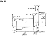
- non-patent reference 9 where a positive voltage for data writing is shown applied to the gate of an FeFET of Pt / Sr Bi 2 Ta 2 O 9 / Hf -Al- O / Si, a diagram is discussed of voltage divisions applied to various portions of a gate and energy bands in directions of depth of the gate. Identically computed, there is derived an energy band diagram ( Fig. 31 ) that is equivalent to that of non-patent reference 9. It is assumed that Pt / Sr Bi 2 Ta 2 O 9 (SBT), Hf -Al- O (HAO) and an interfacial layer (IL) mainly composed of SiO 2 have thicknesses of 200 nm, 7 nm and 3.5 nm, respectively.
- SBT St / Sr Bi 2 Ta 2 O 9
- Hf -Al- O Hf -Al- O
- IL interfacial layer
- the electric polarization at writing is of a degree of 1 to 3 micro C / cm 2 .
- the polarization is greater than of 3 micro C / cm 2 , the voltage and electric field applied to the interfacial layer are increased so that there may develop a phenomenon of injection of electrons from the semiconductor side into the gate insulator side.
- the addition of a phenomenon other than polarization reversal mechanism makes the operation of a FeFET very complicated.
- Non-patent reference 10 discloses a FeFET of Al / PTO / Si where PTO is lead titanate in the form of a film whose thickness is 90 nm. Id - Vd characteristics of FeFET is shown which is obtained on sweeping the gate voltage between - 4 volts and + 4 volts and sweeping it in reciprocation between 1 2 volts and + 2 volts. A data retention property with writing voltages of - 4 and + 4 colts is measured. It is shown that in about 10 4 seconds, it becomes hard to discriminate an On and an Off states. There is no showing of a data retention property with writing voltages of - 2 and + 2 volts, nor is a result shown of rewrite withstand test.
- non-patent reference 11 a Fe FET of TiN / HfSiO / SiO 2 / Si is reported where HfSiO is claimed to be a ferroelectric, having a thickness of 8.5 nm.
- a writing voltage is shown as - 3 and 4 volts and, if a manner of expression of the present invention as mentioned hereinafter is followed, its absolute value is 3.5 volts.
- a data retention property of up to 3 x 10 4 seconds is shown but there is no mention of results of rewrite withstand property.
- an interfacial layer mainly composed of SiO 2 and having a thickness of 3.4 to 5 nm and which is formed on a Si semiconductor surface
- the interfacial layer has a thickness, e. g. of 3.5 nm.
- a voltage of 2.74 volts is applied to the interfacial layer, amounting to 46 % of a gate voltage of 5.95 volts.
- Figs. 30 (a) and (b) are of examples in which the films have thicknesses of 120 nm and 160 nm, respectively.
- FIG. 30(c) shows memory windows of 6 (six) FeFETs of composition Ca 0.2 Sr 0.8 Bi 2 Ta 2 O 9 which are of film thicknesses of 120 nm, 160 nm and 200 nm and are annealed in oxygen at temperatures of 775 and 800 degrees C.
- the same six FeFETs of Fig. 30(c) are measured in sweeping rages of - 0.5 volt to + 0.5 volt.
- Memory windows measured with sleep amplitudes of 3.3 and 5.0 volts are shown in Fig. 30(d) .
- the rate of reduction of a memory window at a sweep amplitude of 3.3 volts down to a memory window at a sweep amplitude of 5.0 volts is at most 38.8 %.
- a sufficient memory window is not obtainable at a sweep amplitude of 3.3 volts.
- the thickness of an interfacial layer across which a voltage is applied is as thick as 3.4 to 5 nm, which made it necessary to apply a surplus writing voltage to cause a phenomenon of electric polarization reversal to develop.
- a sufficient and satisfactory memory window has hitherto been unobtainable.
- P max 2.7 micro C / cm 2
- a reduction of 1 nm of the interfacial layer can be estimated to lead to a decrease of 0.78 volt of the writing voltage.
- the formation and thickness of an interfacial layer may not be enough simply if the time period of annealing is reduced, and the process step of annealing must be one that is sufficient for a ferroelectric layer to develop ferroelectricity.
- a semiconductor ferroelectric memory element less than a gate length of 100 nm requires making a gate laminate less in thickness by photolithography or working technique. Although the thinner, the better; the thickness of a ferroelectric needs to be less than 150 nm.
- the lower limit of the thickness of a ferroelectric is defined as follows: The limit of electric polarization at which the aforementioned phenomenon of injection of electrons may no longer occurs at the time of writing is 3 micro C / cm 2 .
- the method being a method of making a semiconductor ferroelectric memory element, characterized in that: the said film comprises one selected from the class which consists of a film composed of strontium, bismuth, tantalum and oxygen, a film of calcium, strontium, bismuth, tantalum and oxygen, a film of strontium, bismuth, tantalum, niobium and oxygen, and a film of calcium, strontium, bismuth, tantalum, niobium and oxygen; the said metal is composed of one selected from the class which consists of Ir
- the present invention also provides a method of making a semiconductor ferroelectric memory element as set forth above, characterized in that the said semiconductor substrate has a source and a drain region, the said semiconductor ferroelectric memory element being a transistor.
- the said annealing for ferroelectric crystallization is performed preferably at a temperature of not less than 730 degrees Celsius and not more than 800 degrees Celsius.
- the said metal be Ir
- the said mixed gas having oxygen added to nitrogen have oxygen added to nitrogen at a volume proportion of not less than 0.0002 and not more than 0.02.
- the said metal be Pt, and the said mixed gas having oxygen added to nitrogen have oxygen added to nitrogen at a volume proportion of more than 0.0007 and not more than 0.01.
- the said metal be an alloy of Ir and Pt alloyed at a weight proportion of 1 to 1, and the said mixed gas having oxygen added to nitrogen have oxygen added to nitrogen at a volume proportion of more than 0.0001 and not more than 0.0004.
- the said annealing for ferroelectric crystallization is performed, preferably, under a pressure of not less than 0.001 MPa and not more than 1 atmospheric pressure. Note here that 1 atm is equal to 0.1013 Pa.
- the present invention provides a method of making a semiconductor ferroelectric memory element, characterized in that the said insulator is composed of a metal oxide containing at least one of metallic elements of hafnium, zirconium, lanthanum, yttrium, aluminum, magnesium and manganese and comprises a laminate of such metal oxides.
- the present invention provides a method of making a semiconductor ferroelectric memory element, characterized in that the said insulator is of a nitride selected from the class which consists of hafnium nitride and aluminum nitride.
- the present invention provides a method of making a semiconductor ferroelectric memory element, characterized in that the said insulator is selected from the class which consists of one which is composed of the said nitride and the said metal oxide and one which is constituted of a lamination of the said nitride and the said metal oxide laminate.
- the present invention provides a method of making a semiconductor ferroelectric memory element, characterized in that the said nitride is hafnium nitride and the said metal oxide is HfO 2 .
- the said metal oxide is preferably in the form of a film of HfO 2 having a film thickness of not less than 1. 3 nm and not more than 13 nm.
- the present invention provides a method of making a semiconductor ferroelectric memory element, characterized in that the said annealing for ferroelectric crystallization is followed by characteristic adjustment annealing which is at least one of annealing in an oxygen gas and annealing in a mixed gas having hydrogen mixed with nitrogen.
- annealing in the oxygen gas in the characteristic adjustment annealing is effected at an annealing temperature, preferably, of not less than 600 degrees C and not more than 700 degrees C.
- annealing in the mixed gas having hydrogen mixed with nitrogen is effected at an annealing temperature, preferably, of not less than 350 degrees C and not more than 450 degrees C.
- the present invention further provides a method of making a device comprising a semiconductor substrate, an insulator, a ferroelectric and a metal in which the insulator, a film made of constituent elements of a bismuth layer perovskite crystalline ferroelectric and the metal are sequentially formed in the indicated order on a semiconductor substrate and thereafter are subjected to annealing for ferroelectric crystallization, the method being a method of making a semiconductor ferroelectric memory element, characterized in that: the said film comprises one selected from the class which consists of a film composed of strontium, bismuth, tantalum and oxygen, a film of calcium, strontium, bismuth, tantalum and oxygen, a film of strontium, bismuth, tantalum, niobium and oxygen, and a film of calcium, strontium, bismuth, tantalum, niobium and oxygen; the said metal is composed of one selected from the class which consists of Ir, Pt, an alloy of Ir and Pt
- the present invention provides a method of making a semiconductor ferroelectric memory element, characterized in that the said hafnium nitride is formed upon reaction between NH 3 gas and a complex containing Hf in a growth chamber by a metal organic chemical vapor deposition process which comprises the steps of preparing a raw material liquid solution having the complex with Hf dissolved in a solvent; dispersing the raw material liquid solution into a carrier gas to form a raw material gaseous medium in a state of gas and liquid two phases; introducing the raw material gaseous medium while in the state of gas and liquid two phases into a vaporizing chamber to form a vapor thereof; and introducing the vapor into a film forming chamber.
- the said complex that contains hafnium is preferably one of TEMAHF and TDEAHF.
- the present invention provides a semiconductor ferroelectric memory transistor, characterized in that it comprises a semiconductor substrate having a source and a drain region; and an insulator, a ferroelectric and a metal which are layered or laminated in this order on the semiconductor substrate, wherein: the said ferroelectric is one selected from the class which consists of a bismuth layer perovskite ferroelectric composed of strontium, bismuth, tantalum and oxygen, a bismuth layer perovskite ferroelectric composed of calcium, strontium, bismuth, tantalum and oxygen, a bismuth layer perovskite ferroelectric composed of strontium, bismuth, tantalum, niobium and oxygen, and a bismuth layer perovskite ferroelectric composed of calcium, strontium, bismuth, tantalum, niobium and oxygen; the said metal is one selected from the class which consists of Ir, Pt, an alloy of Ir and Pt, and Ru; and the said ferro
- the present invention further provides a semiconductor ferroelectric memory transistor as set forth above, characterized in that it is capable of rewriting data not less than 10 8 times.
- the present invention still further provides a semiconductor ferroelectric memory transistor as set forth in claim 20, characterized in that an interfacial layer is formed between said semiconductor substrate and said insulator and has a thickness of less than 3.4 nm.
- a semiconductor ferroelectric memory element having a laminated structure of an insulator, a ferroelectric and a metal formed on a semiconductor substrate
- preferred conditions are selected for the metal and for the gas in which annealing is effected to crystallize the ferroelectric which adjoins the metal, to reduce the thickness of an interfacial layer mainly composed of SiO 2 and tending to form on surfaces of the semiconductor substrate, whereby an ferroelectric memory element and a transistor having a memory window sufficiently wide at a lower voltage are brought into reality.
- annealing for characteristic adjustment is subsequently effected to achieve a characteristic improvement such as to enlarge the change in drain current with respect to the change in gate voltage.
- Fig. 1 is a sectional view diagrammatically illustrating a course of making a semiconductor ferroelectric memory element made in a first form of implementation of the present invention.
- Numeral 1 designates a semiconductor substrate.
- Fig. 2 is a sectional view diagrammatically illustrating a course of making a semiconductor ferroelectric memory element made in a second form of implementation of the present invention.
- a semiconductor substrate 1 is shown having a source region 6 and a drain region 7.
- the semiconductor substrate 1 is composed of silicon or a semiconductor having a silicon component. It may also be of a mixed crystal of Si and Ge or of SiC. In lieu of a semiconductor substrate, it may also be a SOI (silicon on insulator) substrate.
- Character 3a denotes a layer formed of a composition, as a ferroelectric predecessor, of constituent elements of a Bi layered perovskite crystal structure. Prior to annealing for ferroelectric crystallization, the composition has not yet be of Bi layered perovskite crystal structure.
- Representative are a film made of strontium, bismuth, tantalum and oxygen elements, a film of calcium, strontium, bismuth, tantalum and oxygen, a film of strontium, bismuth, tantalum, niobium and oxygen, and a film of calcium, strontium, bismuth, tantalum, niobium and oxygen.
- Metal 4 may be Ir, Pt, Ru or an alloy of them.
- the film 3a is annealed in a suitable environment for ferroelectric crystallization. This causes its composition to transform into a ferroelectric 3.
- the ferroelectric 3 is composed of a material mainly constituted by a Bi layer perovskite which has been found robust in the fatigue of polarization reversal of ferroelectrics.
- the main constituent of such perovskite may be Sr 2 Bi 2 Ta 2 O 9 ; Ca x Sr 1-x Bi 2 Ta 2 O 9 as a substitute of a part of Sr with Ca in Sr 2 Bi 2 Ta 2 O 9 ; Sr Bi 2 (Ta 1-z Nb z ) 2 O 9 and Ca in Sr 2 Bi 2 Ta 2 O 9 as substitutes of parts of Ta with Nb in Sr 2 Bi 2 Ta 2 O 9 ; Ca x Sr 1-x Bi 2 Ta 2 O 9 and Ca x Sr 1-x Bi 2 Ta 2 O 9 ; Bi 4 Ti 3 O 12 ; (Bi, La) 4 Ti 3 O 12 ; and (Bi, Nd) 4 Ti 3 O 12 .
- Ca x Sr 1-x Bi 2 Ta 2 , Sr Bi 2 (Ta 1-z Nb z ) 2 O 9 and Sr Bi 2 (Ta 1-z Nb z ) 2 O 9 are similar in crystal structure and properties and may interchangeably be used. It has been found that annealing the film 3a after formation of up to the metal 4 on the substrate makes an interfacial region between the ferroelectric 3 and the metal 4 stable in quality, this being connected with and leading to excellent data retention capability and exceeding data rewriting tolerance. Upon zealous investigations in annealing to crystallize the ferroelectric, it has been found important that annealing be performed in the environment of a mixed gas having oxygen added to an inert gas such as N 2 or Ar.
- An interfacial layer 5 mainly composed of SiO 2 is formed on a surface region of the semiconductor substrate 1.
- the term "interfacial layer 5" may hereinafter be so simply termed, suggesting that it be so composed. While the interfacial layer 5 which is of electrical insulating properties can be defined as included in an insulator 2, it may well be regarded as a part of the semiconductor substrate in the present invention. Either way, it is only a question of definition and mode. Electrical conduction in a semiconductor occurs at an interface between the interfacial layer and the internal semiconductor.
- Example 02B of the invention disclosed in Fig. 5 the interfacial layer 5 mainly composed of SiO 2 has a thickness of 2.6 nm.
- a layer denoted by character IL in Fig. 5 is the interfacial layer 5.
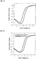
- I d - Vg of the n channel FeFET is disclosed in Fig. 6(a) .
- the drain current is represented in logarithm.
- This FeFET has a gate length (L) of 10 micro-m and a gate width of 200 micro-m.
- Vg is swept in reciprocation between - 3.3 volts and + 3.3 volts.
- V c 0
- a sweep amplitude V amp refers to the absolute value of a data writing voltage into the FeFET. While in measurement of I d - V g the sweep range may hereafter be referred to as Vc ⁇ Vamp, note that it signifies that Vg is swept in reciprocation between V c - V amp and V c + V amp . Along the direction of the arrows as shown, the drain current is changed.
- the drain current (I d ) as shown is normalized for a current per a gate width of 1 micro-m.
- V w V a - V b is equal to 0.59 volt which apparently is wide enough compared with values of the memory window in the prior art (shown in Fig. 30 ).
- the memory window here is markedly widened.
- Example 21C of the invention disclosed in Fig. 7 it is found from a sectional TEM analysis that an interfacial layer 5 mainly composed of SiO 2 has a thickness of 2.5 nm.
- the silicon surface is oxynitrided to a depth of 1.4 nm in an environment of reduced pressure, leaving "SiON (1.4 nm thick) / Si" as it is briefly termed.
- the interfacial layer 5 is formed mainly composed of SiO 2 initially united with a layer of oxynitride of 1.4 nm thick.
- a layer denoted by IL in Fig. 7 is the interfacial layer 5.
- the thickness of the interfacial layer 5 is 2.5 nm which is sufficiently thinner than 3.4 to 5 nm in the prior art.
- Example 02A represents an embodiment of the first form of implementation 1 of the present invention.
- the semiconductor substrate is Si of p type.
- a relationship of electric capacitance with respect to gate voltage: C g -V g is measured, giving a graph shown in Fig. 8 .
- Metal Ir is planar in form and of a square having a side of 100 micro-m.
- the gate voltage after rising from - 3.3 volts to + 3.3 volts is returned to - 3.3 volts.
- An AC voltage having an amplitude of 0.1 volts and an AC frequency of 100 kHz is used.
- a memory window V w of 0.56 volts is evaluated from the C g -V g curves.
- the semiconductor substrate 1 is of silicon or of a semiconductor having a silicon component. It may be a mixed crystal of Si and Ge, or SiC. In lieu of the semiconductor substrate there may be used an SOI (silicon on insulator) substrate.
- SOI silicon on insulator
- the process step of forming the insulator 2 is effected directly upon removal of the surface oxide film, or after the semiconductor substrate surface is nitrided or oxynitrided.
- the nitride or oxynitride film formed has a thickness preferably of not more than 1.5 nm. Any process may be used to make it.
- the surface oxide film is removed by immersion in a solution of buffered or unbuffered fluorinated acid.
- a nitride film may, for example, be formed by introducing NH 3 gas into an atmosphere of reduced pressure and effecting rapid thermal annealing (RTA).
- RTA rapid thermal annealing
- An oxynitride film may, for example, be formed by introducing O 2 gas in an atmosphere of reduced pressure and effecting rapid thermal annealing (RTA) and thereafter introducing NH 3 gas in an atmosphere of reduced pressure and effecting rapid thermal annealing (RTA).
- the insulator 2 is required to be elaborate and to diminish the leakage current between the gate and the semiconductor substrate surface. Further, in the process of making a FeFET, it is also requited, not to cause inter-diffusion of, and to produce no chemical reaction product from, elements of the film 3a, the ferroelectric 3, the semiconductor substrate 1. Further, it is preferred that the insulator 2 be high in dielectric constant so that a gate voltage applied to the FeFET may effectively be applied to the ferroelectric 3.
- the insulator 2 should have an electron affinity (difference in energy between the vacuum level and the lowermost end of conduction bands) smaller than that of the ferroelectric 3, and further that the insulator 2 should have an ionization potential (difference in energy between vacuum level and the uppermost end of conduction bands) larger than that of the ferroelectric 3. If the electron affinity of the insulator 2 is larger than that of the ferroelectric 3, the insulator 2 between the ferroelectric 3 and the interfacial layer 5 mainly composed of SiO 2 on the semiconductor substrate surface tends to become a well for conductive electrons. Due to a leakage current, electrons once they enter the well are hard to come off therefrom; the well providing for a collecting place for incoming electrons.
- the threshold voltage of the FeFET will be caused to shift by a mechanism separate from that of switching between polarizations of the ferroelectric. If the ionization potential of the insulator 2 is lower than that of the ferroelectric, the insulator 2 between the ferroelectric 3 and the interfacial layer 5 mainly composed of SiO 2 on the semiconductor substrate surface tends to become a well for positive holes. Due to a leakage current, positive holes once they enter the well are hard to come off therefrom; the well providing for a collecting place for incoming positive holes.
- the insulator 2 regardless of its kinds if they satisfy these requirements, should preferably be a single oxide or mixed oxides or layered oxides of elements such as hafnium, zirconium, lanthanum, yttrium, aluminum, magnesium and/or manganese. It is also useful to achieve the object of diminishing a leakage current to add nitrogen to the oxides listed.
- the insulator 2 of one or more of aluminum nitride, hafnium nitride, and mixed nitride of aluminum and hafnium, which are found to act to reduce oxygen diffusing into the ferroelectric in the process step of annealing for its crystallization and thus to reduce the extent in which to form an interfacial layer 5 mainly composed of SiO 2 . It is preferable to use a composite compound and layered composite compounds of a nitride such as aluminum nitride, hafnium nitride, or a mixed nitride of aluminum and hafnium and an oxide as an insulator that satisfies the abovementioned requirements as to the insulator 2. In addition, a material may be used that is not an insulator prior to the process step of ferroelectric crystallization annealing and which thereafter comes to satisfy the abovementioned requirements to form the ferroelectric 2.
- an interfacial layer 5 mainly composed of SiO 2 be thinner than 3.4nm as mentioned above, an SiO 2 equivalent film thickness (EOT) of an insulator 2 be also smaller than 3.4 nm and let to stay not less than 0.2 nm and not more than 2 nm, so that a voltage may equally be applied to the interfacial layer 5 and to the insulator 2.
- EOT SiO 2 equivalent film thickness
- An insulator 2 may be formed by any process that meets the abovementioned requirements and may suitably be formed by pulse laser deposition, sputtering, metal organic chemical vapor deposition, atomic layer deposition or the like technique.
- the film 3a is a film composed of elements constituting a Bi layer perovskite. Prior to a process step of crystallization annealing, the film has not yet had a Bi layer perovskite crystal structure.
- Representative of the film 3a are a film of elements of strontium, bismuth, tantalum and oxygen, a film of calcium, strontium, bismuth, tantalum and oxygen, a film of strontium, bismuth, tantalum, niobium and oxygen, and a film of calcium, strontium, bismuth, tantalum, niobium and oxygen, it may also be a film of bismuth, titanium and oxygen, a film of bismuth, tantalum, titanium and oxygen, or a film of bismuth, neodymium, titanium and oxygen.
- the film 3a may be formed by pulse laser deposition, sputtering, or metal chemical vapor deposition, metal organic decomposition (MOD or sol - gel technique or the like.
- the metal 4 may be selected to be a pure metal or an alloy thereof.
- a FeFET that is excellent in data retention property and rewrite withstand property.
- Annealing for ferroelectric crystallization is effected preferably at a temperature of 700 to 820 degrees C and for a time period of 10 to 60 minutes. A material is thus called for to meet the annealing conditions. After zealous investigations, it has been found that Ir, Pt, or an alloy of Ir and Pt, or Ru is suitable.
- metal 4 While there is no particular limitation in how metal 4 is formed, it may be formed, for example, by sputtering, metal organic chemical vapor deposition or electron beam vapor deposition technique.
- the ferroelectric 3 is constituted by a material mainly composed of a Bi layered perovskite that is found robust in fatigue of ferroelectric polarization reversal.
- its main component may be Sr 2 Bi2 Ta 2 O 9 ; Ca x Sr 1-x Bi 2 Ta 2 O 9 as a substitute of a part of Sr with Ca in Sr 2 Bi 2 Ta 2 O 9 ; Sr Bi 2 (Ta 1-z Nb z ) 2 O 9 and Ca in Sr 2 Bi 2 Ta 2 O 9 as substitutes of parts of Ta with Nb in Sr 2 Bi 2 Ta 2 O 9 ; Ca x Sr 1-x Bi 2 Ta 2 O 9 and Ca x Sr 1-x Bi 2 Ta 2 O 9 ; Bi 4 Ti 3 O 12 ; (Bi, La) 4 Ti 3 O 12 ; and (Bi, Nd) 4 Ti 3 O 12 .
- annealing after formation of up to the metal 4 makes an interfacial region between the ferroelectric 3 and the metal 4 stable in quality, this being connected with and leading to excellent data retention capability and exceeding data rewriting tolerance.
- a mixed gas having oxygen added to an inert gas such as N 2 or Ar.
- the ferroelectric 3 which has undergone annealing for ferroelectric crystallization has a Bi layered perovskite crystal structure.
- the ferroelectric should have a thickness df preferably such that 59 nm ⁇ d ⁇ 150 nm.
- an interfacial layer 5 mainly composed of SiO 2 it is important that oxygen as a component of the gaseous atmosphere used in annealing for ferroelectric crystallization should be reduced as much as possible in nitrogen or argon as its main component.
- the ferroelectric being an oxide requires that there exist a degree of oxygen in the atmospheric gas. It is further necessary that metal 4 should withstand the annealing.
- annealing for ferroelectric crystallization is effected at a temperature of 760 degrees C and for a time period of 30 minutes.
- annealing for ferroelectric crystallization is effected at a temperature of 760 degrees C and for a time period of 30 minutes.
- the insulator 2 is of HfO 2 .
- annealing for ferroelectric crystallization is effected at a temperature of 750 degrees C and for a time period of 30 minutes.
- Fig. 11 is a result of measurement of I d - Vg.
- the ferroelectric contains Nb.
- the structure and thickness of a gate laminate are: Ir (75 nm) / Ca 0.2 Sr 0.8 Bi 2 (Ta 0.75 Nb 0.25 ) 2 O 9 (135 nm) / Hf O 2 (5 nm) / Si.
- annealing for ferroelectric crystallization is effected at a temperature of 793 degrees C and for a time period of 30 minutes.
- V w 0.28 volts.
- the insulator 2 is a laminated film having a layer of hafnium nitride having a thickness of 2 nm deposited on Si and a layer of HfO 2 having a thickness of 4 nm deposited on the Hf - N layer .
- annealing for ferroelectric crystallization is effected at a temperature of 780 degrees C and for a time period of 30 minutes.
- the insulator 2 is a laminated film having a layer of hafnium nitride having a thickness of 2 nm deposited on Si and a layer of HfO 2 having a thickness of 4 nm deposited on the Hf - N layer.
- annealing for ferroelectric crystallization is effected at a temperature of 780 degrees C and for a time period of 30 minutes.
- a result of measurement of I d - Vg: with a gate voltage that is swept in a range from - 3.3 volts to + 3.3 volts there is observed a memory window: V w 0.52 volts.
- the insulator 2 is a layer of hafnium nitride having a thickness of 5 nm.
- annealing for ferroelectric crystallization is effected at a temperature of 750 degrees C and for a time period of 30 minutes.
- annealing for ferroelectric crystallization is effected at a temperature of 793 degrees C and for a time period of 30 minutes.
- the insulator 2 is a laminated film formed of a layer of hafnium nitride (Hf - N) deposited on Si and a layer of HfO 2 deposited on the Hf - N layer are put together in Table1.
- the memory window of I d - Vg characteristic has values found with a gate voltage swept from V c - 3.3 volts to V c + 3.3 volts.
- Hf - N is formed by a metal organic chemical vapor deposition (MOCVD) technique.
- the flow of NH 3 should preferably be not less than 9 sccm and not more than 20 sccm. Ranging it so is found to achieve a memory window of not less than 0.4 volt.
- the susceptor temperature should preferably be not less than 260 degrees C and not more than 400 degrees C.
- Hf - N should have a thickness of not less than 1 nm and not more than 3.1 nm. The result of sectional TEM analysis indicates that the thickness of an interfacial layer mainly composed of SiO 2 in Example 11A is 3.1 nm.
- a film of Ir as metal 4 is formed by a sputtering technique and a film 3a by a pulse laser deposition technique.
- hafnium nitride and aluminum nitride are formed by a metal organic chemical vapor deposition technique, and other materials by the pulse laser deposition technique.
- the film 3a is made by the metal organic chemical vapor deposition technique.
- annealing for ferroelectric crystallization is effected at a temperature of 780 degrees C and for a time period of 30 minutes.
- Ir and HfO 2 are formed by the sputtering and pulse laser deposition techniques, respectively.
- Annealing for ferroelectric crystallization may be carried out in an atmosphere having oxygen mixed with an inert gas.
- annealing for ferroelectric crystallization is effected at a temperature of 760 degrees C and for a time period of 30 minutes.
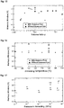
- a volume proportion y of N 2 to O 2 with respect to a memory window in an I d - V g characteristic measured, of a FeFET made using the volume proportion.
- the memory window as a variable along the ordinate axis has values with the gate voltage that is swept in the rage of - 3.3 volts to + 3.3 volts.
- the abscissa axis has a variable y representing a volume proportion of O 2 to N 2 , viz.
- y (volume of O 2 in the mixed gas) / (volume of N 2 in the mixed gas).
- the gases are added at a selected proportion of mixture for ferroelectric crystallization annealing.
- Embodiments indicated by marks ( ⁇ ) in Fig. 15 are the case that annealing is effected in the presence of a flow of nitrogen and oxygen gases. More specifically, the flows of N 2 and O 2 are 1000 and 1000y, respectively.
- Embodiments of marks ( ⁇ ) are the case that annealing is effected in the absence of the flow of nitrogen and oxygen gases. It has been found that favorable conditions to obtain good window are represented by a volume proportion of the gases, regardless of the presence or absence of the gases flowing. With Ir selected for metal 4, a preferred volume proportion of oxygen is not less than 0.0002 and not more than 0.02, achieving a memory window of not less than 0.4 volts.
- an FeFET is made of Ca composition X
- a good memory window is achieved, regardless of presence or absence of gases flowing.
- x 0.25
- Fig. 16 is a graph illustrating a relationship between an annealing temperature in the process step of annealing for ferroelectric crystallization and a memory window in I d - V g characteristic of a FeFET made.
- the memory window as a variable along the ordinate axis has values with the gate voltage that is swept in the rage of - 3.3 volts to + 3.3 volts.
- the time period for annealing is 30 minutes.
- the marks in Fig. 16 individually represent embodiments of FeFET made.
- Embodiments indicated by marks ( ⁇ ) in Fig. 16 are the case that annealing is effected in the presence of a flow of nitrogen and oxygen gases. More specifically, the flows of N 2 and O 2 are 1000 and 1, respectively.
- Embodiments of marks ( ⁇ ) are the case that annealing is effected in the absence of the flow of nitrogen and oxygen gases.
- the preferred temperature conditioned for ferroelectric crystallization annealing is not less than 730 degrees C and not more than 800 degrees C, yielding memory window of not less than 0.4 volts.
- Examples using embodiments of metal 4 other than Ir are shown in Table 4.
- Pt is used for metal 4.
- the memory window is not less than 0.40 volts.
- Fig. 18 is a graph illustrating a relationship between a thickness of HfO 2 used for the insulator 2 and a memory window.
- the marks in Figure individually represent embodiments of FeFET made.
- Embodiments of marks ( ⁇ ) are the case that annealing is effected in the absence of a gaseous flow.
- Embodiments indicated by marks ( ⁇ ) in Fig. 15 are the case that annealing is effected in the presence of the gaseous flow.
- the volume proportion of oxygen gas y 0.0001.
- Fig. 18 shows that the film of HfO 2 (4 nm) most preferably has a thickness of not less than 2 nm and not more than 6 nm.
- the first process is to anneal in oxygen gas under a temperature condition lower than that in annealing for ferroelectric crystallization.
- the second process is to anneal in a gas containing hydrogen.
- the two characteristic adjustment annealing processes may be used in combination.
- annealing is effected at a temperature of not less than 500 degrees C and not more than 700 degrees C for a time period of not less than 10 minutes and not more than 60 minutes.
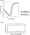
- Fig. 19 discloses the I d - Vg characteristics of one FeFET on the chip in Example 02B before and after the characteristic adjustment annealing. The broken and solid curves represent them before and after the characteristic adjustment. It is seen that with respect to a change in the gate voltage the drain current evidently changes in a region of the gate voltage from to 1 volt, more sharply after the characteristic adjustment annealing than before the characteristic adjustment annealing. The characteristic is improved because of a larger change in current deemed in general better for a narrow change in voltage.
- SS sub - threshold swing
- the SS value is defined as a gate voltage needed to change the drain current by one order of magnitude in a region of voltage lower than the threshold value, and it is better that the SS value is small.
- Fig. 19 (20) discloses the rate of change of the characteristic subsequent to annealing with respect to the temperature in the characteristic adjustment annealing.
- Marked with ⁇ are the rate of change of the memory window, and marked with ⁇ are the rate of change of the S value.
- the rate of change is ([the physical quantity subsequent to annealing] - [the physical quantity prior to annealing]) / [the physical quantity prior to annealing] and represented in per cent (%). It is not good that the rate of the window subsequent to annealing decreases and it is good that the SS value decreases.
- the rate of change of the memory window is small in a range of 500 to 700 degrees C while the SS value diminishes largely as the temperature is risen. A decrease is seen in the SS value to the extent of 10 % in the range of 500 to 700 degrees C.
- the upper limit of annealing temperature in the first process is determined. Annealing in oxygen is deemed to recover a defect in the interface between the interfacial layer and Si.
- the second process makes use of a mixed gas of hydrogen and nitrogen, containing 3 to 5 % of hydrogen.
- the annealing temperature is preferably not less than 350 degrees C and not more than 450 degrees C.
- the annealing time period is preferably not less than 3 minutes and not more than 30 minutes.
- Example 22 shows results of the second process of annealing a FeFET at a temperature of 400 degrees C for a time period of 5 minutes, the FeFET being on the chip in Example 23C.
- the effect of improvement is observed.
- a hydrogen atom coming into a dangling bond between Si and an interfacial layer 5 mainly composed of SiO 2 is deemed to decrease the state density in the interface, causing the effect of hydrogen annealing to be revealed.
- the temperature and period of time are preferably as mentioned above.
- a pulse rewrite withstand property and a data retention capability are disclosed if the writing voltage has its absolute value of 3. 3 volts.
- Use is made of a FeFET in Example 02B.
- An alternating pulse having a cycle of a negatively poled pulse having a height of - 3.3 volts and a width of 10 microseconds followed by a positively poled pulse having a height of + 3.3 volts and a width of 10 microseconds is repetitively applied, constituting rewriting pulses.
- the I d - V g characteristic is measured to examine a rewriting tolerance.
- the gate voltage is swept in reciprocation between - 3.3 and + 3.3 volts.
- Vg is swept from 1.0 volt to 0 volt to obtain an I d - Vg characteristic.
- Vg applied to yield I d 10 -8
- a / micro-m represents a threshold value which is plotted in Fig. 24 .
- the mark ⁇ at after 10 4 seconds and the marks ⁇ at after 10 5 seconds are connected by a straight line (broken line) and extrapolated up to 10 years.
- This extrapolating operation indicates that the difference in threshold voltage after 10 years remains to be about 0.18 volt, showing that two storage states are sufficiently distinguishable from each other. It thus follows that a data retention property equivalent to the data retention property described in patent documents 1 to 3 and non-p references 1 to 9 is met by the present invention.
- the end of a data retention time period refers to a point of time at which two states are no longer distinguishable from each other. It is herein defined as a time at which the difference between the two threshold voltages reaches 0.05 volt.
- the data retention property can also be rated by a method whereby in readout the drain current is measured with the gate voltage fixed.
- the ratio of on current to off current is 3 corresponds virtually to that the difference in threshold voltage is 0.05 volt.
- the end of a data retention time period is defined in a method of measuring a drain current by a time at which the ratio of on current to off current reaches 3. According to this definition, the life of data retention of embodiments of the present invention is enough in excess of 10 years.
- the present invention thus provides a FeFET capable of writing data with a writing voltage whose absolute value is not more than 3.3 volts, without impairing either of two properties which in combination are had by a FeFET which has been developed, the two properties being 1) a data retention property of not less than 10 5 seconds and 2) a data rewrite withstand capability of 10 8 times.
- a Fe FET according to the present invention provides a good device property by a writing voltage even if its absolute value is in excess of 3.3 volts.
- Figs. 25 and 26 show results of a data rewriting tolerance test.
- Fig. 25 is a graph having results from Example 27E.
- Fig. 26 represents results from Example 12H.
- the graph in Fig. 25 is obtained from measurement using the same process as those mentioned above. Only a portion that differs numerically is mentioned.
- An alternating pulse for a cycle of 20 microseconds, constituted of a negatively poled pulse having a height of - 4.5 volts and a width of 10 microseconds followed by a positively poled pulse having a height of + 4.5 volts and a width of 10 microseconds is used.
- a readout operation is performed. In reading out, the gate voltage is swept from 0.6 to - 0.4 volt.
- Fig 26 graphically shows a rewrite withstand capability not less than 10 9 times.
- Figs. 27 and 28 graphically show results of the data retention property.
- Fig. 27 represents results from Example 27F.
- a single negatively poled pulse having a height of - 4.5 volts and a width of 10 microseconds is applied, a state of data retention is entered.
- Vg is swept from 0.3 volt to - 0.4 volt to obtain an I d - Vg characteristic.
- Results of the data readout operation that is likewise performed are shown marked with ⁇ .
- the threshold voltage following the negatively poled pulse is found to be larger by about 0.5 volt higher than the threshold voltage following the positively poled pulse. showing a good data retention property.
- Fig. 28 shows results from Example 12H. Thickness of a gate laminate and condition of annealing for ferroelectric crystallization of the Example 12H are as mentioned above.
- the negatively poled pulse for writing has a height of - 4.5 volts and a width of 10 microseconds.
- the positively poled pulse for writing has a height of + 4.5 volts and a width of 10 microseconds.
- a source and a drain region are formed and a Si substrate of p - type covered with a SiO 2 surface layer having a thickness of 35 nm is prepared.
- the substrate is immersed in buffered hydrofluoric acid to remove the protective SiO 2 film on its surface, a state as shown in Fig. 29(a) .
- a pulse laser deposition technique is used to form an insulator 2.
- Its target is HfO2 and the laser is KrF excimer laser, having a wavelength of 248 nm, a pulse projection number of 10 per second and a laser energy of 250 mJ.
- the substrate is held at a temperature of 220 degrees C, and N 2 is introduced at a rate of flow of 4 sccm and under a pressure of 15 Pa and for a time period of 8 minutes and 57 seconds.
- the insulator 2 is formed in the form of a film of HfO 2 . Note that the rate of forming the film varying with the state of equipment and target is seized separately by a monitor. The film forming time is adjusted to give a selected film thickness.
- a pulse laser deposition technique is used to form a film 3a.
- the target is Ca - Sr - Bi - Ta - O.
- the laser is KrF excimer laser, having a wavelength of 246 nm, a pulse projection number of 50 per second and a laser energy of 250 mJ.
- the substrate is held at a temperature of 415 degrees C, and O 2 is introduced at a rate of flow of 3.1 sccm and under a pressure of 11 Pa and for a time period of 17 minutes and 47 seconds to form a film 3a.
- the film 3a formed is of Ca - Sr - Bi - Ta - O. Note that the rate of forming the film varying with the state of equipment and target is seized separately by a monitor. The film forming time is adjusted to give a selected film thickness.
- An Rf magnetron scattering technique is used to form a metal 4.
- the target is metal Ir and the substrate is not heated.
- Argon is introduced at a rate of flow of 1.4 sccm and under a pressure of 0.15 Pa.
- Rf power is 40 W and held for 22 minutes and 30 seconds to form a film of Ir having a thickness of 75 nm, as the metal.
- Past process steps 2, 3 and 4 a state as shown in Fig. 29(b) is had.
- a photoresist of the gate configuration is left by an ordinary photographic technique.
- FeFETs of 8 kinds have a gate length of 10 micrometers and a gate width of 200 to 10 micrometers
- An ion milling technique is used to remove portions of Ir metal which are not covered with the photoresist.
- Example specimen is immersed in acetone to remove the photoresist, the specimen being thereafter cleansed in ultrapure water, bringing about a state as shown in Fig. 29c ).
- An infrared gold-image furnace is used to perform annealing for ferroelectric crystallization.
- the Example specimen has a temperature risen from room temperature to 750 degrees C for a time period of 10 minutes and is annealed at the temperature of 750 degrees C under a pressure of 1 atm in the absence of flow for a time period of 30 minutes.
- An ordinary photolithographic technique is used to remove the resist at a portion of the hole for contact of the source and drain.
- An ion milling technique is used to remove portions of the ferroelectric and insulator 2.
- Example specimen is immersed in acetone to remove the photoresist.
- a state as shown in Fig. 29(d) is reached, making it possible to measure an I d - V g characteristic and others.
- the process step of annealing for ferroelectric crystallization is effected intervening between the process steps of Fig. 29(c) and2(d) , transforming the film 3a in Fig. 29(c) into a ferroelectric 3.
- the interfacial layer 5 mainly composed of SiO 2 is omitted from illustration.
- the two sorts of annealing may be performed at need and after process steps 6 and 7.
- this Example has hafnium nitride (Hf - N) formed having a thickness of 2 nm and thereafter HfO 2 formed having a thickness of 4 nm. Forming of HfO 2 is the same as in Example 302B. However, the time period for film forming is varied in consideration of a change in rate of film forming.
- a film of hafnium nitride (Hf - N) is formed using a metal organic chemical vapor deposition technique of the type in which a raw material liquid solution is prepared having a complex compound containing Hf and dissolved in a solvent, the raw material liquid solution being dispersed into a carrier gas to form a raw material gaseous medium in a state of gas and liquid two phases; the raw material gaseous medium while in the state of gas and liquid two phases is introduced into a vaporizing chamber to form a vapor thereof; and the vapor is introduced into a film forming chamber.
- the complex compound containing Hf is preferably Hf [N (C 2 H 5 ) (CH 3 )] 4 , tetrakis - dimethyl amino hafnium, which is abbreviated as TEMAHF. It can be confirmed that a complex compound expressed by chemical formula: Hf (N (C 2 H 5 ) 2 ] 4 , tetrakis diethyl-amido hafnium abbreviated as TDEAHF can also be used to form a film of Hf-N.
- TDEAHF tetrakis diethyl-amido hafnium
- EHC ethyl cyclohexane
- the carrier gas uses nitrogen gas, but may be argon gas. Ammonia (NH 3 ) gas is also introduced in to the growth chamber.
- the concentration of TEMAHF in ECT is preferably 0.1 mol to 0.2 mol per liter.
- the concentration of TDEAHF in ECT is preferably 0.1 mol to 0.2 mol per liter.
- the rate of liquid flow of the raw material liquid solution is preferably 0.1 to ccm to 0.3 ccm.
- the pressure of the growth chamber is 200 Pa to 700 Pa.
- the rate of NH 3 gas is not less than 5 sccm and not more than 30 sccm, and the susceptor temperature is not less than 260 degrees C and not more than 400 degrees C, it has been found that they are preferable to form a film of hafnium nitride satisfying a stoichiometric mixture ratio of Hf 3 N 4 .
Landscapes
- Engineering & Computer Science (AREA)
- Computer Hardware Design (AREA)
- Chemical & Material Sciences (AREA)
- Non-Volatile Memory (AREA)
- Semiconductor Memories (AREA)
- Materials Engineering (AREA)
- Crystallography & Structural Chemistry (AREA)
- Chemical Kinetics & Catalysis (AREA)
- Physics & Mathematics (AREA)
- Optics & Photonics (AREA)
- Formation Of Insulating Films (AREA)
Abstract
Description
- The present invention relates to a method of making a semiconductor ferroelectric memory element and to a semiconductor ferroelectric memory transistor. More specifically, it relates to a semiconductor ferroelectric memory transistor operable under a reduced voltage and to a method of making such a semiconductor ferroelectric memory element.
- A ferroelectric-gate field effect transistor (FeFET) incorporating a ferroelectric in its gate insulator has come to be attracting attention as a transistor having a memory function. While having long had the problem that its data storage time is short, in
patent document 1 an FeFET is shown in which the gate laminate of electrode conductor / ferroelectric / insulator / semiconductor is comprised of metal Pt, SBT (Sr Bi2 Ta2 O9) as a sort of crystal of Bi layered perovskite structure, insulator Hf - Al - O and semiconductor Si, thus of Pt / Sr Bi2 Ta2 O9 / Hf - Al - O2 / Si. An example of the FeFET is disclosed there in which both the on and off states of a drain current when each measured for a long period of time are continued extremely stably and the ratio of drain currents in the on state and off state after a weak reaches not less than 105. In the same patent document, a good data retention property is disclosed of a FeFET composed of Pt / Sr Bi2 Ta2 O9 / Hf O2 / Si, too. Thus, it has been demonstrated bypatent document 1 that a FeFET acts as a memory transistor in which data is truly retained and stored. In the same patent document, data rewrite withstand property is evaluated and it is disclosed that after rewriting 1012 times, the on time and off states read out are fully discriminated. While a reason for such good data rewrite withstand capability has not yet been clarified, it is deemed to be due to the fact that the ferroelectric is made up of crystal of Bi layer perovskite structure. In the Bi layered perovskite structure, ferroelectricity (i.e. the property that atoms are distorted according to a direction of electric field and after the electric field is removed, the distortion is left and electric polarization is not restored to zero) occurs at portions of the perovskite structure. It appears that a Bi layered oxide substance between the perovskite portions acting as a buffer layer renders a malfunction less liable to occur at an interface with another layer such as of Pt, in data rewriting, to wit, during a repetition of the reversal of electric field for writing, thus leading to the good rewrite withstand capability of a FeFET. - In
patent document 2, there is disclosed a FeFET using (Bi, Nd)4 Ti3 O12 that is a Bi layer perovskite substance, as the ferroelectric. Non-patentreference 1 discloses the use in FeFETs of (Bi, La)4 Ti3 O12 that is a Bi layer perovskite substance, as the ferroelectric. -
Patent document 3 discloses using CSBT (CaxSr1-x Bi2 Ta2 O9) as the ferroelectric of Bi layer perovskite substance, and that a FeFET composed of Pt / Cax Sr1-x Bi2 Ta2 O9 / Hf - Al- O /Si processes a good data retention property and a good data rewrite withstand capability. - Upon forming Bi layer perovskite on the insulator / semiconductor, annealing is performed in an oxygen atmosphere for a time period of 10 to 60 minutes to crystallize the Bi layer perovskite, thereby causing it to express the ferroelectricity. It is performed at a temperature preferably from 700 to 830 degrees Celsius, more preferably from 730 to 813 degrees C. Passing the process step of annealing is found to achieve a good data retention and a good rewrite withstand property as mentioned above. By passing the process step of annealing, an interfacial layer is formed at an interface between silicon and the insulator as shown by
non-patent reference 2 to 4. Non-patentreference 3 teaches that the interfacial layer is formed mainly composed of SiO2. This connotes that in annealing in an oxygen atmosphere for crystallizing the Bi layer perovskite, a silicon surface is oxidized to form the interfacial layer mainly composed of SiO2. As a result of uniform formation of the interfacial layer, it contributes to development of good electrical characteristics. Non-patentreference 5 discloses an example of development of an NAND flash memory of 64 k bitts with a FeFET as a memory cell by this technique. - There are the following reports of dividing the insulator into two layers. In
non-patent reference 6, a film of silicon nitride is formed on silicon and thereafter a film of HfO2 is formed. Innon-patent reference 7, a film of oxynitride of silicon is formed on silicon and thereafter HfO2 is formed. In either case, passing the process step of annealing to crystallize the Bi layer perovskite and to develop the ferroelectricity causes an interfacial layer mainly composed of SiO2 to be formed between Si and HfO2. The interfacial layer may contain nitrogen as derived from the film of silicon nitride and/or the film of oxynitride of silicon but is mainly composed of SiO2. The interfacial layer is formed mainly by oxidation of Si, but may be merged with the insulating layer, and may have an insulating material contained therein as an impurity. Note that whilenon-patent reference 7 shows the range in which the gate voltage is swept is from 1 - 3.3 volts to 1 + 3.3 volts, the data given there teaches that the ferroelectric SBT has a thickness as thick as 450 nm and is not suitable for a FeFET to be nanofined. - There is a report regarding the thickness of an interfacial layer which is inspected with a transmission electron microscope as mainly composed of SiO2. Non-patent
reference 2 shows that a FeFET composed of Pt / Sr Bi2 Ta2 O9 / Hf - Al - O / Si annealed in oxygen at a temperature of 800 degrees C and for a time period of 60 minutes has an interfacial layer having a thickness of 4.4 nm. Althoughpatent document 2 discloses that SiO2 having a thickness of 2 nm to 5 nm is provided between Hf2 and Si, it is not the thickness of an interfacial layer mainly composed of SiO2, but is the thickness of SiO2 in the insulator prior to annealing for ferroelectric crystallization. There is no mention of the thickness of an interfacial layer mainly composed of SiO2 subsequent to annealing which is effected at a temperature of 700 to 800 degrees C in an oxygen atmosphere for a time period of 30 minutes for the purposes of annealing for ferroelectric crystallization. - In
patent reference 8, it is shown that annealed in oxygen at a temperature of 750 degrees C for a time period of 30 minutes, a laminate constituted of a film of (Bi, La)4 Ti3 O12 having a thickness of 400 nm on a film of HfO2 having a thickness of 8 nm on Si has an interfacial layer having a thickness of about 5 nm. Innon-patent reference 4, it is shown that a FeFET composed of Pt / Cax Sr1-X Bi2 Ta2 O9 / Hf - Al - O / Si annealed in oxygen at a temperature of 778 degrees C for a time period of 30 minutes has an interfacial layer having a thickness of 3.4 nm. Innon-patent reference 6, it is shown that a gate laminate composed of Pt / Sr Bi2 Ta2 O9 / HfO2 / SiN / Si is annealed in oxygen at a temperature of 800 degrees C for a time period of 1 hour, forming an interfacial layer mainly composed of SiO2 and having a thickness of 4 nm. Thus, annealing in oxygen at a temperature of 750 to 800 degrees C for a time period of 30 to 60 minutes is shown to form an interfacial layer having a thickness of 3.4 nm to 5 nm. Further lowering the annealing temperature is shown to tend to decrease the thickness of an interfacial layer and to produce a FeFET whose electrical characteristics are not good. A FeFET presenting acceptable characteristics is shown to have an interfacial layer having a thickness of 3.4 nm to 5 nm. - In reducing a FeFET in size, it is required from the technique of microfining such as etching that the height of a gate laminate be reduced. As shown in
patent document 1 andnon-patent references 6 to 8, the thickness of a ferroelectric is commonly 400 nm or more. While inpatent reference 3 Examples are almost of a film of ferroelectric Cax Sr1-x Bi2 Ta2 having a thickness of 200 nm, an Example is shown in which the film thickness is 120 nm. However, the writing voltage is used which in absolute value is as high as 5 volts. - In
non-patent reference 9, where a positive voltage for data writing is shown applied to the gate of an FeFET of Pt / Sr Bi2 Ta2 O9 / Hf -Al- O / Si, a diagram is discussed of voltage divisions applied to various portions of a gate and energy bands in directions of depth of the gate. Identically computed, there is derived an energy band diagram (Fig. 31 ) that is equivalent to that ofnon-patent reference 9. It is assumed that Pt / Sr Bi2 Ta2 O9 (SBT), Hf -Al- O (HAO) and an interfacial layer (IL) mainly composed of SiO2 have thicknesses of 200 nm, 7 nm and 3.5 nm, respectively. If it is then assumed that when a writing voltage is applied, an electric polarization of Pmax = 2.7 micro C / cm2 is formed in a ferroelectric, an equivalent charge is induced on the gate electrode Pt, and a voltage of 1.20 volts is applied to the ferroelectric, a voltage of 1.06 volts to Hf - Al - O, a voltage of 2.74 volt to the interfacial layer and a surface electrostatic potential of 0.95 volt to Si. A voltage of 5.95 volts as a sum of them is applied the gate metal, Pt. The voltage Vil of 2.74 volts applied to the interfacial layer is derived from dil Pmax / ( ε 0 kil) (= 2.74 V) where dil is a thickness of the interfacial layer mainly composed of SiO2, and kil is a dielectric constant of the interfacial layer, for which use is made of that of 3.9 of SiO2, and ε 0 is the dielectric constant in vacuum. The electric polarization at writing is of a degree of 1 to 3 micro C / cm2. If the polarization is greater than of 3 micro C / cm2, the voltage and electric field applied to the interfacial layer are increased so that there may develop a phenomenon of injection of electrons from the semiconductor side into the gate insulator side. The addition of a phenomenon other than polarization reversal mechanism makes the operation of a FeFET very complicated. - Non-patent
reference 10 discloses a FeFET of Al / PTO / Si where PTO is lead titanate in the form of a film whose thickness is 90 nm. Id - Vd characteristics of FeFET is shown which is obtained on sweeping the gate voltage between - 4 volts and + 4 volts and sweeping it in reciprocation between 1 2 volts and + 2 volts. A data retention property with writing voltages of - 4 and + 4 colts is measured. It is shown that in about 104 seconds, it becomes hard to discriminate an On and an Off states. There is no showing of a data retention property with writing voltages of - 2 and + 2 volts, nor is a result shown of rewrite withstand test. Innon-patent reference 11, a Fe FET of TiN / HfSiO / SiO2 / Si is reported where HfSiO is claimed to be a ferroelectric, having a thickness of 8.5 nm. A writing voltage is shown as - 3 and 4 volts and, if a manner of expression of the present invention as mentioned hereinafter is followed, its absolute value is 3.5 volts. A data retention property of up to 3 x 10⁴ seconds is shown but there is no mention of results of rewrite withstand property. -
- [patent document 1]
JP 2004 - 304143 A - [patent document 2]
JP 2006 - 108648 A - [patent Document 3]
WO / 2013 / 183547 -
- [non-patent ref. 1] Applied Physics Letters, vol. 85, pages 399 - 3201, published in 2004
- [non-p ref. 2] Japanese Journal of Applied Physics, vol. 43, pages 7876 - 7878, published in 2004
- [non-p ref. 3] IEEE International Electron Devices Meeting Technical Digest, pages 915 - 918, published in 2004
- [non-p ref. 4] Semiconductor Science and Technology, vol. 28, MS No. (pages): 085003 (7), published in 2013
- [non-p ref. 5] Japanese Journal of Applied Physics, vol. 51, MS No. (pages); 04DD01 (7), published in 2012
- [non-p ref. 6] Semiconductor Science and Technology, vol. 24, MS No. (pages): 105026 (5), published in 2009
- [non-p ref. 7] Semiconductor Science and Technology, vol. 25, MS No. (pages): 055005 (5), published in 2009
- [non-p ref. 8] Japanese Journal of Applied Physics, vol. 44, pages 6218 - 6220, published in 2005
- [non-p ref. 9] IEEE Non-Volatile Memory Technology Symposium 2012 Proceeding, pages 55 - 59, published in 2013
- [non-p ref. 10] Applied Physics Letters, vol. 85, pages 4726 - 4728, published in 2004
- [non-p ref. 11] IEEE International Electron Devices Meeting Digest, pages 547 - 550, published in 2011
- According to the prior art as mentioned above, as for an interfacial layer mainly composed of SiO2 and having a thickness of 3.4 to 5 nm and which is formed on a Si semiconductor surface, assume that the interfacial layer has a thickness, e. g. of 3.5 nm. Then, if the ferroelectric at the time of writing has a polarization of 2.7 micro C / cm2, it follows that a voltage of 2.74 volts is applied to the interfacial layer, amounting to 46 % of a gate voltage of 5.95 volts. This necessarily requires the writing voltage as shown in
non-patent reference 5, i.e. the operating voltage to be as high as 6 to 7 volts. While this voltage is enough lower than that of a NAND flash memory with a memory cell comprising a field effect transistor having a floating gate using a voltage of around 20 volts for writing, it is demanded that a FeFET operate at a voltage which is still more reduced to meet a diversity of needs. - Of a FeFET made in the prior art, let it be assumed that the gate voltage is swept in reciprocation in a range between - 2.3 volts and + 4.3 volts (i.e. in a range between 0.5 - 3.3 volts and 0.5 + 3.3 volts at a sweep amplitude of 3.3 volts). Then, the drain current is as shown in
Figs. 30 (a) and (b) from which it is seen that the memory window as a width between hysteresis curves is smaller than 0.26 volt.Figs. 30(a) and (b) are of examples in which the films have thicknesses of 120 nm and 160 nm, respectively.Fig. 30(c) shows memory windows of 6 (six) FeFETs of composition Ca0.2 Sr0.8 Bi2 Ta2 O9 which are of film thicknesses of 120 nm, 160 nm and 200 nm and are annealed in oxygen at temperatures of 775 and 800 degrees C. The same six FeFETs ofFig. 30(c) are measured in sweeping rages of - 0.5 volt to + 0.5 volt. Memory windows measured with sleep amplitudes of 3.3 and 5.0 volts are shown inFig. 30(d) . The rate of reduction of a memory window at a sweep amplitude of 3.3 volts down to a memory window at a sweep amplitude of 5.0 volts is at most 38.8 %. Thus, of a FeFET made by the prior art, a sufficient memory window is not obtainable at a sweep amplitude of 3.3 volts. In the prior art, the thickness of an interfacial layer across which a voltage is applied is as thick as 3.4 to 5 nm, which made it necessary to apply a surplus writing voltage to cause a phenomenon of electric polarization reversal to develop. Hence, with a small sweep amplitude of 3.3 volts, a sufficient and satisfactory memory window has hitherto been unobtainable. - Assuming that the thickness of an interfacial layer mainly composed of SiO2 can be reduced by Δ, the writing voltage can be reduced by Δ Vil = Δ dil x Pmax / ( ε 0kil). And, assuming that the ferroelectric polarization at writing: Pmax = 2.7 micro C / cm2, a reduction of 1 nm of the interfacial layer can be estimated to lead to a decrease of 0.78 volt of the writing voltage. The formation and thickness of an interfacial layer may not be enough simply if the time period of annealing is reduced, and the process step of annealing must be one that is sufficient for a ferroelectric layer to develop ferroelectricity. Making a semiconductor ferroelectric memory element less than a gate length of 100 nm (or nano-fining the element) requires making a gate laminate less in thickness by photolithography or working technique. Although the thinner, the better; the thickness of a ferroelectric needs to be less than 150 nm. The lower limit of the thickness of a ferroelectric is defined as follows: The limit of electric polarization at which the aforementioned phenomenon of injection of electrons may no longer occurs at the time of writing is 3 micro C / cm2. The coercive electric field Ec of ferroelectric SBT (Sr Bi2 Ta2 O9) in reciprocal sweeping between + 3 micro C / cm2 and - 3 micro C / cm2 for metal / SBT / metal is known to be about 33 kV / cm. If the film thickness necessary to obtain a memory window of 0.39 volt is defined as the lower limit in film thickness, it follows that from Vw / (2Ec) = 0.39 / (2ES), the lower limit of film thickness can be estimated to be 59 nm. Since Ec of Cax Sr1-x Bi2 Ta2 O9 is more than that of SBT, its lower limit in film thickness comes to be further lowered.
- It is accordingly an object of the present invention to provide a FeFET and a method of its making, the FeFET having a ferroelectric whose film thickness (dr) is made small and so nanofine as to range in: 59 nm < dr < 150, without impairing the data retention property of not less than 105 seconds and the data rewrite withstand property of not less than 108 times of FeFETs that have hitherto been developed, and the FeFET allowing data to be written with a writing voltage whose absolute value is not more than 3.3 volts.
- In order to achieve the object mentioned above, there is provided in accordance with the present invention a method of making a device comprising a semiconductor substrate, an insulator, a ferroelectric and a metal in which the insulator, a film made of constituent elements of a bismuth layer perovskite crystalline ferroelectric and the metal are sequentially formed in the indicated order on the semiconductor substrate and thereafter are subjected to annealing for ferroelectric crystallization, the method being a method of making a semiconductor ferroelectric memory element, characterized in that: the said film comprises one selected from the class which consists of a film composed of strontium, bismuth, tantalum and oxygen, a film of calcium, strontium, bismuth, tantalum and oxygen, a film of strontium, bismuth, tantalum, niobium and oxygen, and a film of calcium, strontium, bismuth, tantalum, niobium and oxygen; the said metal is composed of one selected from the class which consists of Ir, Pt, an alloy of Ir and Pt, and R; and said annealing for ferroelectric crystallization is performed in a mixed gas selected from the class which consists of one having oxygen added to nitrogen and one having oxygen added to argon.
- The present invention also provides a method of making a semiconductor ferroelectric memory element as set forth above, characterized in that the said semiconductor substrate has a source and a drain region, the said semiconductor ferroelectric memory element being a transistor.
- Further, according to the invention the said annealing for ferroelectric crystallization is performed preferably at a temperature of not less than 730 degrees Celsius and not more than 800 degrees Celsius.
- Also, it is preferred according to the invention that the said metal be Ir, and the said mixed gas having oxygen added to nitrogen have oxygen added to nitrogen at a volume proportion of not less than 0.0002 and not more than 0.02.
- Alternatively, it is also preferred according to the invention that the said metal be Pt, and the said mixed gas having oxygen added to nitrogen have oxygen added to nitrogen at a volume proportion of more than 0.0007 and not more than 0.01.
- Alternatively, it is also preferred according to the invention that the said metal be an alloy of Ir and Pt alloyed at a weight proportion of 1 to 1, and the said mixed gas having oxygen added to nitrogen have oxygen added to nitrogen at a volume proportion of more than 0.0001 and not more than 0.0004.
- According to the invention, the said annealing for ferroelectric crystallization is performed, preferably, under a pressure of not less than 0.001 MPa and not more than 1 atmospheric pressure. Note here that 1 atm is equal to 0.1013 Pa.
- Also, the present invention provides a method of making a semiconductor ferroelectric memory element, characterized in that the said insulator is composed of a metal oxide containing at least one of metallic elements of hafnium, zirconium, lanthanum, yttrium, aluminum, magnesium and manganese and comprises a laminate of such metal oxides.
- Also, the present invention provides a method of making a semiconductor ferroelectric memory element, characterized in that the said insulator is of a nitride selected from the class which consists of hafnium nitride and aluminum nitride.
- Further, the present invention provides a method of making a semiconductor ferroelectric memory element, characterized in that the said insulator is selected from the class which consists of one which is composed of the said nitride and the said metal oxide and one which is constituted of a lamination of the said nitride and the said metal oxide laminate.
- Further, the present invention provides a method of making a semiconductor ferroelectric memory element, characterized in that the said nitride is hafnium nitride and the said metal oxide is HfO2.
- According to the present invention, the said metal oxide is preferably in the form of a film of HfO2 having a film thickness of not less than 1. 3 nm and not more than 13 nm.
- Also, the present invention provides a method of making a semiconductor ferroelectric memory element, characterized in that the said annealing for ferroelectric crystallization is followed by characteristic adjustment annealing which is at least one of annealing in an oxygen gas and annealing in a mixed gas having hydrogen mixed with nitrogen.
- Further, according to the invention, annealing in the oxygen gas in the characteristic adjustment annealing is effected at an annealing temperature, preferably, of not less than 600 degrees C and not more than 700 degrees C.
- Also, according to the invention, in characteristic adjustment annealing, annealing in the mixed gas having hydrogen mixed with nitrogen is effected at an annealing temperature, preferably, of not less than 350 degrees C and not more than 450 degrees C.
- The present invention further provides a method of making a device comprising a semiconductor substrate, an insulator, a ferroelectric and a metal in which the insulator, a film made of constituent elements of a bismuth layer perovskite crystalline ferroelectric and the metal are sequentially formed in the indicated order on a semiconductor substrate and thereafter are subjected to annealing for ferroelectric crystallization, the method being a method of making a semiconductor ferroelectric memory element, characterized in that: the said film comprises one selected from the class which consists of a film composed of strontium, bismuth, tantalum and oxygen, a film of calcium, strontium, bismuth, tantalum and oxygen, a film of strontium, bismuth, tantalum, niobium and oxygen, and a film of calcium, strontium, bismuth, tantalum, niobium and oxygen; the said metal is composed of one selected from the class which consists of Ir, Pt, an alloy of Ir and Pt, and R; and the said annealing for ferroelectric crystallization is performed in an oxygen atmosphere under a pressure of not less than 10 Pa and not more than 100 Pa.
- Also, the present invention provides a method of making a semiconductor ferroelectric memory element, characterized in that the said hafnium nitride is formed upon reaction between NH3 gas and a complex containing Hf in a growth chamber by a metal organic chemical vapor deposition process which comprises the steps of preparing a raw material liquid solution having the complex with Hf dissolved in a solvent; dispersing the raw material liquid solution into a carrier gas to form a raw material gaseous medium in a state of gas and liquid two phases; introducing the raw material gaseous medium while in the state of gas and liquid two phases into a vaporizing chamber to form a vapor thereof; and introducing the vapor into a film forming chamber.
- Further, according to the invention the said complex that contains hafnium is preferably one of TEMAHF and TDEAHF.
- Also, the present invention provides a semiconductor ferroelectric memory transistor, characterized in that it comprises a semiconductor substrate having a source and a drain region; and an insulator, a ferroelectric and a metal which are layered or laminated in this order on the semiconductor substrate, wherein: the said ferroelectric is one selected from the class which consists of a bismuth layer perovskite ferroelectric composed of strontium, bismuth, tantalum and oxygen, a bismuth layer perovskite ferroelectric composed of calcium, strontium, bismuth, tantalum and oxygen, a bismuth layer perovskite ferroelectric composed of strontium, bismuth, tantalum, niobium and oxygen, and a bismuth layer perovskite ferroelectric composed of calcium, strontium, bismuth, tantalum, niobium and oxygen; the said metal is one selected from the class which consists of Ir, Pt, an alloy of Ir and Pt, and Ru; and the said ferroelectric has a film thickness of more than 59 nm and less than 150 nm, the said semiconductor ferroelectric memory element being usable to write data with a writing voltage whose absolute value is not more than 3.3 volts, and having an ability to retain data for a time period of not less than 105 seconds.
- The present invention further provides a semiconductor ferroelectric memory transistor as set forth above, characterized in that it is capable of rewriting data not less than 108 times.
- The present invention still further provides a semiconductor ferroelectric memory transistor as set forth in
claim 20, characterized in that an interfacial layer is formed between said semiconductor substrate and said insulator and has a thickness of less than 3.4 nm. - In a semiconductor ferroelectric memory element having a laminated structure of an insulator, a ferroelectric and a metal formed on a semiconductor substrate, preferred conditions are selected for the metal and for the gas in which annealing is effected to crystallize the ferroelectric which adjoins the metal, to reduce the thickness of an interfacial layer mainly composed of SiO2 and tending to form on surfaces of the semiconductor substrate, whereby an ferroelectric memory element and a transistor having a memory window sufficiently wide at a lower voltage are brought into reality. Furthermore, annealing for characteristic adjustment is subsequently effected to achieve a characteristic improvement such as to enlarge the change in drain current with respect to the change in gate voltage.
-
- [
Fig. 1 ] It is a sectional view illustrating a step in making a semiconductor ferroelectric memory element made in a first form of implementation of the present invention. - [
Fig. 2 ] It is a sectional view illustrating a step in making a semiconductor ferroelectric memory element made in a second form of implementation of the present invention. - [
Fig. 3 ] It is a sectional view of the semiconductor ferroelectric memory element made in the first form of implementation of the present invention. - [
Fig. 4 ] It is a sectional view of the semiconductor ferroelectric memory element made in the second form of implementation of the present invention. - [
Fig. 5 ] It is a sectional TEM photograph of Example 02B of the invention. - [
Fig. 6 ] It includes a graph (a) representing a relationship between a drain current and a gate voltage of a FeFET in Example 02B of the present invention and a graph (b) representing a relationship between a sweep amplitude Vamp and a memory window. - [
Fig. 7 ] It is a sectional TEM photograph of Example 21C of the invention. - [
Fig. 8 ] It is a graphical representation of an electric capacitance with respect to a gate voltage between metal and a semiconductor substrate in Example 02A of the invention. - [
Fig. 9 ] It shows a relationship between a drain current and a gate voltage in Example 26C of the invention in which the gate lamination has a structure and a thickness of Ir (75 nm) / CSBT (x = 0.2, 135 nm) / Hf - La - Al - O (5 nm) / Si, having the insulator 5 (I layer) of a composition ratio of HfO2: LaAlO3 = 7: 3. - [
Fig. 10 ] It is a graph illustrating a relationship between a drain current and a gate voltage in Example 16A of the invention in which the gate lamination has a structure and a thickness of Ir (75 nm) / CSBT (x = 0.25, 135 nm) / Zr- Y - O (5 nm) / Si, having the insulator 5 (I layer) of Zr - Y - O. - [
Fig. 11 ] It is a graph illustrating a relationship between a drain current and a gate voltage in Example 302B of the invention in which the gate lamination has a structure and a thickness of Ir (75 nm) / CSBT (x = 0.2, 135 nm) / HfO2 (4 nm) / Si. - [
Fig. 12 ] It is a graph illustrating a relationship between a drain current and a gate voltage in Example 12B of the invention in which the gate lamination has a structure and a thickness of Ir (75 nm) / CSBT (x = 0.2, 135 nm) / HfO2 (4 nm) / Si. - [
Fig. 13 ] It is a graph illustrating a relationship between a drain current and a gate voltage in Example 09F of the invention in which the gate lamination has a structure and a thickness of Ir (75 nm) / CSBT (x = 0.15, 120 nm) / HfO2 (5 nm) / Si. - [
Fig. 14 ] It is a graph illustrating a relationship between a drain current and a gate voltage in Example 03C of the invention in which the gate lamination has a structure and a thickness of Ir (75 nm) / CSBT (x = 0.2, 135 nm) / Hf - Mg - O (5 nm) / Si. Annealing for crystallization is performed in Ar - O2. - [
Fig. 15 ] It is a graph illustrating a relationship between a volume proportion of O2 to N2 in annealing for ferroelectric crystallization and a memory window of Id - Vg characteristic in an embodiment of FeFET made using the volume proportion andmetal 4 of Ir, according to the present invention. - [
Fig. 16 ] It is a graph illustrating a relationship between an annealing temperature of the process of annealing for ferroelectric crystallization and a memory window of Id - Vg characteristic of a FeFET made according to the present invention. - [
Fig. 17 ] It is a graph in summary of Examples of the invention in which annealing for ferroelectric crystallization is performed in the environment of a pressure lower than one atmospheric pressure in accordance with the present invention. - [
Fig. 18 ] It is a graph illustrating a relationship between a thickness of HfO2 used for theinsulator 2 and a memory window, according to the present invention. - [
Fig. 19 ] It is a graph illustrating Id - Vg characteristics before and after annealing in a first process of characteristic adjustment annealing in Example 02B of the invention. - [
Fig. 20 ] It is a graph illustrating a relationship between an annealing temperature in the first process and a rate of change of memory window and a rate of change of SS value, according to the present invention. - [
Fig. 21 ] It is a graph illustrating relationships between a drain current and a gate voltage after (solid curve), and between those before (broken curve), annealing in a second process of characteristic adjustment is performed at a temperature of 400 degrees C and a time period of 30 minutes in Example 21C of the invention. - [
Fig. 22 ] It is a graph illustrating relationships between a drain current and a gate voltage after (solid curve), and between those before (broken curve), annealing in a second process of characteristic adjustment is performed at a temperature of 400 degrees C and a time period of 5 minutes in Example 23C of the invention. - [
Fig. 23 ] It is a graph illustrating results of data rewrite withstand tests for Example 02B of the invention, using rewrite pulses alternating between - 3.3 volts and + 3.3 volts. - [
Fig. 24 ] It is a graph illustrating results of measurement of data retention property for Example 02B (with rewrite voltages of + 3.3 volts) of the invention. - [
Fig. 25 ] It is a graph illustrating results of data rewrite withstand tests for Example 27E of the invention. - [
Fig. 26 ] It is a graph illustrating results of data rewrite withstand tests for Example 12H of the invention. - [
Fig. 27 ] It is a graph illustrating results of data rewrite withstand tests for Example 27F of the invention. - [
Fig. 28 ] It is a graph illustrating results of data rewrite withstand tests for Example 12H of the invention. - [
Fig. 29 ] It is an explanatory view illustrating a process of making an Example 302B of the invention. - [
Fig. 30 ] It illustrates properties of FeFETs made by the prior art, including a graph (a) illustrating a relationship between a drain current and a gate voltage of a FeFET made of a ferroelectric of Ca0.2 Sr0.8 Bi2 Ta2 O9 and having a film thickness of 120 nm, a graph (b) illustrating that of a FeFET made of a ferroelectric of Ca0.2 Sr0.8 Bi2 Ta2 O9 and having a film thickness of 160 nm, (c) a graph illustrating a relationship between a memory window and a film thickness of prior-art FeFETs made of Ca0.2 Sr0.8 Bi2 Ta2 O9 and of 120 nm, 160 nm and 200 nm thick in which marked by ○ and ● are ones annealed for 30 minutes at temperatures of 775 and 800 degrees C, respectively, and to obtain a memory window, a gate voltage sweep range I is set at 0.5 volts ± 3.3 volts, and a graph (d) illustrating a memory window with respect to a sweep amplitude of 3.3 volts and 5.0 volts. - [
Fig. 31 ] It is a diagram illustrating energy and voltage divisions found depth-wise at various gate parts when a positive data rewrite voltage is applied to the gate of FeFET composed of Pt / Sr Bi2 Ta2 O9 / Hf - Al - O / Si. -
Fig. 1 is a sectional view diagrammatically illustrating a course of making a semiconductor ferroelectric memory element made in a first form of implementation of the present invention.Numeral 1 designates a semiconductor substrate.Fig. 2 is a sectional view diagrammatically illustrating a course of making a semiconductor ferroelectric memory element made in a second form of implementation of the present invention. In the second form of implementation, asemiconductor substrate 1 is shown having asource region 6 and adrain region 7. Thesemiconductor substrate 1 is composed of silicon or a semiconductor having a silicon component. It may also be of a mixed crystal of Si and Ge or of SiC. In lieu of a semiconductor substrate, it may also be a SOI (silicon on insulator) substrate.Character 3a denotes a layer formed of a composition, as a ferroelectric predecessor, of constituent elements of a Bi layered perovskite crystal structure. Prior to annealing for ferroelectric crystallization, the composition has not yet be of Bi layered perovskite crystal structure. Representative are a film made of strontium, bismuth, tantalum and oxygen elements, a film of calcium, strontium, bismuth, tantalum and oxygen, a film of strontium, bismuth, tantalum, niobium and oxygen, and a film of calcium, strontium, bismuth, tantalum, niobium and oxygen. It may also be a film of bismuth, titan and oxygen, a film of bismuth, lanthanum, titanium and oxygen or a film of bismuth, neodymium, titanium and oxygen.Metal 4 may be Ir, Pt, Ru or an alloy of them. - After up to the meal are formed, the
film 3a is annealed in a suitable environment for ferroelectric crystallization. This causes its composition to transform into a ferroelectric 3. The ferroelectric 3 is composed of a material mainly constituted by a Bi layer perovskite which has been found robust in the fatigue of polarization reversal of ferroelectrics. In accordance with a composition of elements of the film, the main constituent of such perovskite may be Sr2 Bi2 Ta2 O9; Cax Sr1-x Bi2 Ta2 O9 as a substitute of a part of Sr with Ca in Sr2 Bi2 Ta2 O9; Sr Bi2 (Ta1-z Nbz)2 O9 and Ca in Sr2 Bi2 Ta2 O9 as substitutes of parts of Ta with Nb in Sr2 Bi2 Ta2 O9; Cax Sr1-x Bi2 Ta2 O9 and Cax Sr1-x Bi2 Ta2 O9; Bi4 Ti3 O12; (Bi, La)4 Ti3 O12; and (Bi, Nd)4 Ti3 O12. Cax Sr1-x Bi2 Ta2, Sr Bi2 (Ta1-z Nbz)2 O9 and Sr Bi2 (Ta1-z Nbz)2 O9 are similar in crystal structure and properties and may interchangeably be used. It has been found that annealing thefilm 3a after formation of up to themetal 4 on the substrate makes an interfacial region between the ferroelectric 3 and themetal 4 stable in quality, this being connected with and leading to excellent data retention capability and exceeding data rewriting tolerance. Upon zealous investigations in annealing to crystallize the ferroelectric, it has been found important that annealing be performed in the environment of a mixed gas having oxygen added to an inert gas such as N2 or Ar. Passing through the annealing to crystallize the ferroelectric, the first form of implementation comes out whose cross section is diagrammatically shown inFig. 3 , Passing through the annealing to crystallize the ferroelectric, the second form of implementation comes out whose cross section is diagrammatically shown inFig. 4 . Aninterfacial layer 5 mainly composed of SiO2 is formed on a surface region of thesemiconductor substrate 1. The term "interfacial layer 5" may hereinafter be so simply termed, suggesting that it be so composed. While theinterfacial layer 5 which is of electrical insulating properties can be defined as included in aninsulator 2, it may well be regarded as a part of the semiconductor substrate in the present invention. Either way, it is only a question of definition and mode. Electrical conduction in a semiconductor occurs at an interface between the interfacial layer and the internal semiconductor. - An embodiment of the invention that has been annealed for the ferroelectric crystallization is analyzed using a sectional transmission electron microscope (sectional TEM) and it has been found possible that the
interfacial layer 5 mainly composed of SiO2 be made thinner than 3.4 nm. In Example 02B of the invention disclosed inFig. 5 , theinterfacial layer 5 mainly composed of SiO2 has a thickness of 2.6 nm. A layer denoted by character IL inFig. 5 is theinterfacial layer 5. A FeFET in this Example has Ir having a thickness of 75 nm, CSBT (Ca Sr Bi Ta) of x = 0.2 having a thickness of 135 nm and HfO2 having a thickness of 4 nm, which are formed on the semiconductor substrate. A ferroelectric of CSBT of x = 0.2 signifies that the ferroelectric is mainly composed of Cax Sr1-x Bi2 Ta2 O9 where x = 0.2. This gate lamination is referred to briefly as Ir (75 nm) / CSBT (x=0.2, 135 nm) / HfO2 (4 nm) / Si. This brief reference will hereinafter be used suitably to the extent that it brings about no confusion. The relationship between a drain current and a gate voltage: Id - Vg of the n channel FeFET is disclosed inFig. 6(a) . The drain current is represented in logarithm. This FeFET has a gate length (L) of 10 micro-m and a gate width of 200 micro-m. Vg is swept around a center Vc = 0 volt, with a sweep amplitude Vamp = 3.3 V and in a sweep range which is Vc + Vamp = 3.3 volts from Vc - Vamp = - 3.3 volts. Vg is swept in reciprocation between - 3.3 volts and + 3.3 volts. While there are Examples, too, hereafter in which measurement is made with Vc that is not zero, it is ensured to achieve Vc = 0 by suitably selecting the kind and concentration of an impurity on the side of a semiconductor in the use of such technique as ion implantation. Note that a sweep amplitude Vamp refers to the absolute value of a data writing voltage into the FeFET. While in measurement of Id - Vg the sweep range may hereafter be referred to as Vc ± Vamp, note that it signifies that Vg is swept in reciprocation between Vc - Vamp and Vc + Vamp. Along the direction of the arrows as shown, the drain current is changed. The drain current (Id) as shown is normalized for a current per a gate width of 1 micro-m. In achieving this Id - Vg relationship, the drain voltage (Vd), source voltage (Vs), and substrate voltage (Vsub) are so conditioned that Vd = 0.1 volt and Vs = Vsub = 0 volt. Hereafter, unless otherwise indicated, an Id - Vg relationship is measured under such Vd, Vs and Vsub voltage conditions. If threshold voltages are defined as corresponding to Id = 1 x 10⁻⁸ amperes per micro-m, inFig. 6(a) they are seen to be gate voltages Va and Vb at points (a) and (b), respectively. If a difference between them is defined as a memory window Vw, it is seen inFig. 6(a) that Vw = Va - Vb is equal to 0.59 volt which apparently is wide enough compared with values of the memory window in the prior art (shown inFig. 30 ). InFig. 6(b) there is shown a relationship between a sweep amplitude and a memory window. It is shown that at Vamp = 2.7 volts, = 3.6 volts and = 3.9 volts, Vw = 0.40 volts, = 0.69 volts and = 079 volts, respectively. Compared with those of the prior art shown inFig. 30d , the memory window here is markedly widened. Especially, even at a small writing voltage as Vamp = 2.7 volts, it becomes apparent that Vw = 0.40 volts. These manifest improvements are apparently due to a reduction in thickness of the interfacial layer down to a thickness of 2.6 nm which should lower the voltage applied thereto in data writing, thereby permitting an inversion in electric polarization to be initiated at a lower writing voltage. - In Example 21C of the invention disclosed in
Fig. 7 , it is found from a sectional TEM analysis that aninterfacial layer 5 mainly composed of SiO2 has a thickness of 2.5 nm. In this Example, on asemiconductor substrate 1 after an oxide film on its surface is removed by a buffered hydroacid fluoride, the silicon surface is oxynitrided to a depth of 1.4 nm in an environment of reduced pressure, leaving "SiON (1.4 nm thick) / Si" as it is briefly termed. The lamination or structure of layers in this Example comprises a metal layer of Ir having a thickness of 150 nm, a ferroelectric layer of CSBT where x = 0.2, and an insulator layer of HfO2 having a thickness of 6 nm. As disclosed inFig. 7 , theinterfacial layer 5 is formed mainly composed of SiO2 initially united with a layer of oxynitride of 1.4 nm thick. A layer denoted by IL inFig. 7 is theinterfacial layer 5. The thickness of theinterfacial layer 5 is 2.5 nm which is sufficiently thinner than 3.4 to 5 nm in the prior art. - Example 02A represents an embodiment of the first form of
implementation 1 of the present invention. The laminated gate structure comprises Ir (75 nm) / CSBT (x = 0, 2.135 nm) / HfO2 (4 nm) / Si. The semiconductor substrate is Si of p type. A relationship of electric capacitance with respect to gate voltage: Cg-Vg is measured, giving a graph shown inFig. 8 . Metal Ir is planar in form and of a square having a side of 100 micro-m. The gate voltage after rising from - 3.3 volts to + 3.3 volts is returned to - 3.3 volts. An AC voltage having an amplitude of 0.1 volts and an AC frequency of 100 kHz is used. As seen from the Figure, a memory window Vw of 0.56 volts is evaluated from the Cg-Vg curves. Vw is evaluated with a gate voltage where Cg = 100 F / cm2. - Explanation is given in detail of forming of the laminated structure.
- The
semiconductor substrate 1 is of silicon or of a semiconductor having a silicon component. It may be a mixed crystal of Si and Ge, or SiC. In lieu of the semiconductor substrate there may be used an SOI (silicon on insulator) substrate. Prior to attaching aninsulator 2 to the semiconductor substrate, it is important that an oxide film on its surface be removed. The process step of forming theinsulator 2 is effected directly upon removal of the surface oxide film, or after the semiconductor substrate surface is nitrided or oxynitrided. The nitride or oxynitride film formed has a thickness preferably of not more than 1.5 nm. Any process may be used to make it. For example, the surface oxide film is removed by immersion in a solution of buffered or unbuffered fluorinated acid. A nitride film may, for example, be formed by introducing NH3 gas into an atmosphere of reduced pressure and effecting rapid thermal annealing (RTA). An oxynitride film may, for example, be formed by introducing O2 gas in an atmosphere of reduced pressure and effecting rapid thermal annealing (RTA) and thereafter introducing NH3 gas in an atmosphere of reduced pressure and effecting rapid thermal annealing (RTA). - The
insulator 2 is required to be elaborate and to diminish the leakage current between the gate and the semiconductor substrate surface. Further, in the process of making a FeFET, it is also requited, not to cause inter-diffusion of, and to produce no chemical reaction product from, elements of thefilm 3a, the ferroelectric 3, thesemiconductor substrate 1. Further, it is preferred that theinsulator 2 be high in dielectric constant so that a gate voltage applied to the FeFET may effectively be applied to the ferroelectric 3. Furthermore, it is preferred that theinsulator 2 should have an electron affinity (difference in energy between the vacuum level and the lowermost end of conduction bands) smaller than that of the ferroelectric 3, and further that theinsulator 2 should have an ionization potential (difference in energy between vacuum level and the uppermost end of conduction bands) larger than that of the ferroelectric 3. If the electron affinity of theinsulator 2 is larger than that of the ferroelectric 3, theinsulator 2 between the ferroelectric 3 and theinterfacial layer 5 mainly composed of SiO2 on the semiconductor substrate surface tends to become a well for conductive electrons. Due to a leakage current, electrons once they enter the well are hard to come off therefrom; the well providing for a collecting place for incoming electrons. As a result, electrons are extant in theinsulator 2, and if they change, the threshold voltage of the FeFET will be caused to shift by a mechanism separate from that of switching between polarizations of the ferroelectric. If the ionization potential of theinsulator 2 is lower than that of the ferroelectric, theinsulator 2 between the ferroelectric 3 and theinterfacial layer 5 mainly composed of SiO2 on the semiconductor substrate surface tends to become a well for positive holes. Due to a leakage current, positive holes once they enter the well are hard to come off therefrom; the well providing for a collecting place for incoming positive holes. As a result, positive holes are extant in theinsulator 2, and if they change, the threshold voltage of the FeFET will be caused to shift by a mechanism separate from that of switching between polarizations of the ferroelectric. Note further that since the height of a barrier of SiO2 as of Si for electrons is smaller than for positive holes and injection of charges from the semiconductor substrate into theinsulator 2 is more prone to occur with electrons than with positive holes, it is preferred that the electron affinity of theinsulator 2 should be smaller than that of the ferroelectric 3, than that the ionization potential of theinsulator 2 should be higher than that of the ferroelectric 3. Theinsulator 2, regardless of its kinds if they satisfy these requirements, should preferably be a single oxide or mixed oxides or layered oxides of elements such as hafnium, zirconium, lanthanum, yttrium, aluminum, magnesium and/or manganese. It is also useful to achieve the object of diminishing a leakage current to add nitrogen to the oxides listed. It is also preferable to compose theinsulator 2 of one or more of aluminum nitride, hafnium nitride, and mixed nitride of aluminum and hafnium, which are found to act to reduce oxygen diffusing into the ferroelectric in the process step of annealing for its crystallization and thus to reduce the extent in which to form aninterfacial layer 5 mainly composed of SiO2. It is preferable to use a composite compound and layered composite compounds of a nitride such as aluminum nitride, hafnium nitride, or a mixed nitride of aluminum and hafnium and an oxide as an insulator that satisfies the abovementioned requirements as to theinsulator 2. In addition, a material may be used that is not an insulator prior to the process step of ferroelectric crystallization annealing and which thereafter comes to satisfy the abovementioned requirements to form the ferroelectric 2. - Since it is preferred that an
interfacial layer 5 mainly composed of SiO2 be thinner than 3.4nm as mentioned above, an SiO2 equivalent film thickness (EOT) of aninsulator 2 be also smaller than 3.4 nm and let to stay not less than 0.2 nm and not more than 2 nm, so that a voltage may equally be applied to theinterfacial layer 5 and to theinsulator 2. Denoting a specific dielectric constant of theinsulator 2 as kin and a dielectric constant of SiO2 as ksio2, it follows that the insulator has an actual film thickness of di = (kin / ksio2) * EOT. Using kin = 25 and k sio2 = 3.9 if theinsulator 2 is HfO2, it is seen that an actual film thickness of HfO2 that corresponds to the EOT that is not less than 0. 2 nm and not more than 2 nm becomes not less than 1.3 nm and not more than13 nm. - An
insulator 2 may be formed by any process that meets the abovementioned requirements and may suitably be formed by pulse laser deposition, sputtering, metal organic chemical vapor deposition, atomic layer deposition or the like technique. - The
film 3a is a film composed of elements constituting a Bi layer perovskite. Prior to a process step of crystallization annealing, the film has not yet had a Bi layer perovskite crystal structure. Representative of thefilm 3a are a film of elements of strontium, bismuth, tantalum and oxygen, a film of calcium, strontium, bismuth, tantalum and oxygen, a film of strontium, bismuth, tantalum, niobium and oxygen, and a film of calcium, strontium, bismuth, tantalum, niobium and oxygen, it may also be a film of bismuth, titanium and oxygen, a film of bismuth, tantalum, titanium and oxygen, or a film of bismuth, neodymium, titanium and oxygen. - The
film 3a may be formed by pulse laser deposition, sputtering, or metal chemical vapor deposition, metal organic decomposition (MOD or sol - gel technique or the like. - The
metal 4 may be selected to be a pure metal or an alloy thereof. By formingmetal 4 on thefilm 3a and thereafter annealing the film to effect ferroelectric crystallization, there is yielded a FeFET that is excellent in data retention property and rewrite withstand property. Annealing for ferroelectric crystallization is effected preferably at a temperature of 700 to 820 degrees C and for a time period of 10 to 60 minutes. A material is thus called for to meet the annealing conditions, After zealous investigations, it has been found that Ir, Pt, or an alloy of Ir and Pt, or Ru is suitable. - While there is no particular limitation in how
metal 4 is formed, it may be formed, for example, by sputtering, metal organic chemical vapor deposition or electron beam vapor deposition technique. - After
metal 4 is formed, annealing for ferroelectric crystallization is effected in a suitable temperature environment. This will transform thefilm 3a into a ferroelectric 3. The ferroelectric 3 is constituted by a material mainly composed of a Bi layered perovskite that is found robust in fatigue of ferroelectric polarization reversal. According to a composition of elements of thefilm 3a, its main component may be Sr2 Bi2 Ta2 O9; Cax Sr1-x Bi2 Ta2 O9 as a substitute of a part of Sr with Ca in Sr2 Bi2 Ta2 O9; Sr Bi2 (Ta1-z Nbz)2 O9 and Ca in Sr2 Bi2 Ta2 O9 as substitutes of parts of Ta with Nb in Sr2 Bi2 Ta2 O9; Cax Sr1-x Bi2 Ta2 O9 and Cax Sr1-x Bi2 Ta2 O9; Bi4 Ti3 O12; (Bi, La)4 Ti3 O12; and (Bi, Nd)4 Ti3 O12. It has been found that annealing after formation of up to themetal 4 makes an interfacial region between the ferroelectric 3 and themetal 4 stable in quality, this being connected with and leading to excellent data retention capability and exceeding data rewriting tolerance. Upon zealous investigations, in annealing to crystallize the ferroelectric it has been found important that it be performed in the environment of a mixed gas having oxygen added to an inert gas such as N2 or Ar. It has been confirmed by an X - ray analysis process that the ferroelectric 3 which has undergone annealing for ferroelectric crystallization has a Bi layered perovskite crystal structure. The ferroelectric should have a thickness df preferably such that 59 nm < d < 150 nm. More specifically, to lessen forming aninterfacial layer 5 mainly composed of SiO2, it is important that oxygen as a component of the gaseous atmosphere used in annealing for ferroelectric crystallization should be reduced as much as possible in nitrogen or argon as its main component. At the same time, in order to transform thefilm 3a into a ferroelectric 3 of Bi layer perovskite, the ferroelectric being an oxide requires that there exist a degree of oxygen in the atmospheric gas. It is further necessary thatmetal 4 should withstand the annealing. With Ir, Pt, an alloy of Ir and Pt, and Ru there are available suitable amounts, respectively, of oxygen gas. - Forming of the laminated structure is disclosed below in detail through Examples of the invention. In Example 26C, the
insulator 2 is of a composite oxide of hafnium, lanthanum and aluminum: (Hf - La - Al - O), having a makeup molar ratio, HfO2: LaAlO3 = 7: 3. The structure and thickness of a gate laminate are: Ir (75 nm) / CSBT (x = 0.2, 135 nm) / Hf - La - Al - O (5 nm) / Si. In an atmosphere having oxygen mixed with N2 (the volume ratio of N2 to O2 being 1: 0.001), annealing for ferroelectric crystallization is effected at a temperature of 760 degrees C and for a time period of 30 minutes.Fig. 9 is a result of measurement of Id - Vg. With a gate voltage that is swept in a range from - 3.3 volts to + 3.3 volts there is observed a memory window: Vw = 0.49 volts. In Example 16A, theinsulator 2 is of a composite oxide of zirconium and yttrium: (Zr - Y - O), having a makeup molar ratio, ZrO2: Y2O3 = 92: 8. The structure and thickness of a gate laminate are: Ir (75 nm) / CSBT (x = 0.25, 135 nm) / Zr - Y - O (5 nm) / Si. In an atmosphere having oxygen mixed with N2 (the volume ratio of N2 to O2 being 1: 0.001), annealing for ferroelectric crystallization is effected at a temperature of 760 degrees C and for a time period of 30 minutes.Fig. 10 is a result of measurement of Id - Vg. With a gate voltage that is swept in a range from - 3.3 volts to + 3.3 volts there is observed a memory window: Vw = 0.37 volts. In Example 302B, theinsulator 2 is of HfO2. The structure and thickness of a gate laminate are: Ir (75 nm) / CSBT (x = 0.2, 135 nm) / Hf O2- (4 nm) / Si. In an atmosphere having oxygen mixed with N2 (the volume ratio of N2 to O2 being 1: 0.001), annealing for ferroelectric crystallization is effected at a temperature of 750 degrees C and for a time period of 30 minutes.Fig. 11 is a result of measurement of Id - Vg. With a gate voltage that is swept in a range from 0.5 - 3.3 volts to 0.5 + 3.3 volts there is observed a memory window: Vw = 0.64 volts. In Example 20C, the ferroelectric contains Nb. The structure and thickness of a gate laminate are: Ir (75 nm) / Ca0.2 Sr0.8 Bi2 (Ta0.75 Nb0.25)2 O9 (135 nm) / Hf O2 (5 nm) / Si. In an atmosphere having oxygen mixed with N2 (the volume ratio of N2 to O2 being 1: 0.001), annealing for ferroelectric crystallization is effected at a temperature of 793 degrees C and for a time period of 30 minutes. With a gate voltage that is swept in a range from - 3.3 volts to + 3.3 volts there is observed a memory window: Vw = 0.28 volts. - In Example 12B, the
insulator 2 is a laminated film having a layer of hafnium nitride having a thickness of 2 nm deposited on Si and a layer of HfO2 having a thickness of 4 nm deposited on the Hf - N layer .The structure and thickness of a gate laminate are: Ir (75 nm) / CSBT (x = 0.2, 135 nm) / HfO2 (4 nm) / Hf - N (2 nm) / Si. In an atmosphere having oxygen mixed with N2 (the volume ratio of N2 to O2 being 1: 0.001), annealing for ferroelectric crystallization is effected at a temperature of 780 degrees C and for a time period of 30 minutes.Fig. 12 is a result of measurement of Id - Vg. With a gate voltage that is swept in a range from 0.5 - 3.3 volts to 0.5 + 3.3 volts there is observed a memory window: Vw = 0.57 volts. In Example 25C, theinsulator 2 is a laminated film having a layer of hafnium nitride having a thickness of 2 nm deposited on Si and a layer of HfO2 having a thickness of 4 nm deposited on the Hf - N layer. The structure and thickness of a gate laminate are: Ir (75 nm) / CSBT (x = 0.2, 135 nm) / HfO2 (4 nm) / Al - N (2 nm) / Si. In an atmosphere having oxygen mixed with N2 (the volume ratio of N2 to O2 being 1: 0.001), annealing for ferroelectric crystallization is effected at a temperature of 780 degrees C and for a time period of 30 minutes. A result of measurement of Id - Vg: with a gate voltage that is swept in a range from - 3.3 volts to + 3.3 volts there is observed a memory window: Vw = 0.52 volts. In Example 18C, theinsulator 2 is a layer of hafnium nitride having a thickness of 5 nm. The structure and thickness of a gate laminate are: Ir (75 nm) / CSBT (x = 0.2, 135 nm) / Hf - N (4 nm) / Si. In an atmosphere having oxygen mixed with N2 (the volume ratio of N2 to O2 being 1: 0.0006), annealing for ferroelectric crystallization is effected at a temperature of 750 degrees C and for a time period of 30 minutes. A result of measurement of Id - Vg: with a gate voltage that is swept in a range from - 3.3 volts to + 3.3 volts there is observed a memory window: Vw = 0.39 volts. Example 402A is an Example in which use is made of CSBT of x = 0.3. The structure and thickness of a gate laminate are: Ir (75 nm) / CSBT (x = 0.3, 135 nm) / Hf O2- (5 nm) / Si. In an atmosphere having oxygen mixed with N2, annealing for ferroelectric crystallization is effected at a temperature of 793 degrees C and for a time period of 30 minutes. A result of measurement of Id - Vg: with a gate voltage that is swept in a range from - 3.3 volts to + 3.3 volts there is observed a memory window: Vw = 0.42 volts. - Results of Examples in which likewise in Example 12B, the
insulator 2 is a laminated film formed of a layer of hafnium nitride (Hf - N) deposited on Si and a layer of HfO2 deposited on the Hf - N layer are put together in Table1. The gate laminate is structured commonly of Ir / CSBT (x = 0.2) / HfO2 / Hf - N / Si. The memory window of Id - Vg characteristic has values found with a gate voltage swept from Vc - 3.3 volts to Vc + 3.3 volts. Hf - N is formed by a metal organic chemical vapor deposition (MOCVD) technique. Making conditions becoming a key to the MOCVD technique respectively for the Examples are listed in Table 1. The flow of NH3 should preferably be not less than 9 sccm and not more than 20 sccm. Ranging it so is found to achieve a memory window of not less than 0.4 volt. Also, the susceptor temperature should preferably be not less than 260 degrees C and not more than 400 degrees C. Hf - N should have a thickness of not less than 1 nm and not more than 3.1 nm. The result of sectional TEM analysis indicates that the thickness of an interfacial layer mainly composed of SiO2 in Example 11A is 3.1 nm. - In Examples 02B, 21C, 02A, 26C, 16A, 302B and 12B, a film of Ir as
metal 4 is formed by a sputtering technique and afilm 3a by a pulse laser deposition technique. Of theinsulator 2, hafnium nitride and aluminum nitride are formed by a metal organic chemical vapor deposition technique, and other materials by the pulse laser deposition technique. In Example 09F, thefilm 3a is made by the metal organic chemical vapor deposition technique. CSBT as the ferroelectric 3 has a thickness of 120 nm and has a Ca composition x where x = 0.15. The structure and thickness of a gate laminate are Ir (75 nm) / CSBT (x = 0.15, 120 nm) / HfO2 (5 nm) / Si. In an atmosphere having oxygen mixed with N2 (the volume ratio of N2 to O2 being 1: 0.00026, annealing for ferroelectric crystallization is effected at a temperature of 780 degrees C and for a time period of 30 minutes.Fig. 13 is a result of measurement of Id - Vg. With a gate voltage that is swept in a range from 0.5 - 3.3 volts to 0.5 + 3.3 volts there is observed a memory window: Vw = 0.51 volts. In Example 09F, Ir and HfO2 are formed by the sputtering and pulse laser deposition techniques, respectively. - Annealing for ferroelectric crystallization may be carried out in an atmosphere having oxygen mixed with an inert gas. In Example 030C, The
insulator 2 is of a composite oxide of hafnium and magnesium (Hf - Mg - O), having a makeup molar ratio of HfO2: MgO = 7: 3. The structure and thickness of a gate laminate are Ir (75 nm) / CSBT (x = 0.2, 135 nm) / Hf - Mg - O (5 nm) / Si. In an atmosphere having oxygen mixed with Ar (the volume ratio of Ar to O2 being 1: 0.001), annealing for ferroelectric crystallization is effected at a temperature of 760 degrees C and for a time period of 30 minutes.Fig. 14 is a result of measurement of Id - Vg. With a gate voltage that is swept in a range from - 3.3 volts to + 3.3 volts there is observed a memory window: Vw = 0.44 volts. - For annealing to crystallize a ferroelectric, investigations have been made in detail of the atmosphere having oxygen gas O2 mixed with N2 gas, the temperature and the pressure. First, with Ir used for
metal 4 there has been found a relationship, as shown inFig. 15 , of a volume proportion y of N2 to O2 with respect to a memory window in an Id - Vg characteristic measured, of a FeFET made using the volume proportion. The memory window as a variable along the ordinate axis has values with the gate voltage that is swept in the rage of - 3.3 volts to + 3.3 volts. The abscissa axis has a variable y representing a volume proportion of O2 to N2, viz. that y = (volume of O2 in the mixed gas) / (volume of N2 in the mixed gas). The marks inFig. 15 individually represent embodiments of FeFET made. Commonly to all embodiments inFig. 15 , The structure and thickness of a gate laminate are Ir (75 nm) / CSBT (x = 0.2, 135 nm) / HfO2 (4 nm) / Si, and the temperature and the time period of annealing to crystallize the ferroelectric are 780 degrees C and 30 minutes, respectively. Ir and is formed by the sputtering technique, and CSBT and HfO2 are formed by the pulse laser deposition technique. After the annealing vessel is once evacuated to a vacuum, the gases are added at a selected proportion of mixture for ferroelectric crystallization annealing. Embodiments indicated by marks (▲) inFig. 15 are the case that annealing is effected in the presence of a flow of nitrogen and oxygen gases. More specifically, the flows of N2 and O2 are 1000 and 1000y, respectively. Embodiments of marks (■) are the case that annealing is effected in the absence of the flow of nitrogen and oxygen gases. It has been found that favorable conditions to obtain good window are represented by a volume proportion of the gases, regardless of the presence or absence of the gases flowing. With Ir selected formetal 4, a preferred volume proportion of oxygen is not less than 0.0002 and not more than 0.02, achieving a memory window of not less than 0.4 volts. - In other embodiments, too, in which an FeFET is made of Ca composition X, a good memory window is achieved, regardless of presence or absence of gases flowing. In Example 24A, x = 0.25, and the gate laminate is of Ir (75 nm) / CSBT (x = 0.25, 135) / HfO2 (4 nm) / Si. Annealing for ferroelectric crystallization is performed under conditions of: without gases flowing, y = 0.01, 780 degrees C and 30 minutes, yielding a memory window of 0.51 volts with the gate voltage that is swept in a rage from - 3.3 volts to + 3.3 volts. In Example 24B, x = 0.25, and the gate laminate is of Ir (75 nm) / CSBT (x = 0.25, 135) / HfO2 (4 nm) / Si. Annealing for ferroelectric crystallization is performed under conditions of in the presence of gases flowing, y = 0.01, 780 degrees C and 30 minutes, yielding a memory window of 0.51 volts with the gate voltage that is swept in a rage from - 3.3 volts to + 3.3 volts. In Example 24B, x = 0.25, and the gate laminate is of Ir (75 nm) / CSBT (x = 0.25, 135) / HfO2 (4 nm) / Si. Annealing for ferroelectric crystallization is performed under conditions of in the presence of gases flowing, y = 0.01, 780 degrees C and 30 minutes, yielding a memory window of 0.48 volts with the gate voltage that is swept in a rage from - 3.3 volts to + 3.3 volts.
-
Fig. 16 is a graph illustrating a relationship between an annealing temperature in the process step of annealing for ferroelectric crystallization and a memory window in Id - Vg characteristic of a FeFET made. The memory window as a variable along the ordinate axis has values with the gate voltage that is swept in the rage of - 3.3 volts to + 3.3 volts. The time period for annealing is 30 minutes. The marks inFig. 16 individually represent embodiments of FeFET made. Embodiments indicated by marks (▲) inFig. 16 are the case that annealing is effected in the presence of a flow of nitrogen and oxygen gases. More specifically, the flows of N2 and O2 are 1000 and 1, respectively. Embodiments of marks (■) are the case that annealing is effected in the absence of the flow of nitrogen and oxygen gases. In the embodiments marked with (▲), the structure and thickness of a gate laminate are of Ir (75 nm) / CSBT (x = 0.2, 135 nm) / HfO2 (5 nm) / Si. The structure and thickness of a gate laminate in the embodiments marked with (■) are of Ir (75 nm) / CSBT (x = 0.2, 135) / HfO2 (4 nm) / Si. The preferred temperature conditioned for ferroelectric crystallization annealing is not less than 730 degrees C and not more than 800 degrees C, yielding memory window of not less than 0.4 volts. - Examples using embodiments of
metal 4 other than Ir are shown in Table 4. In Examples 22A, 22B, 22C, 19E, 19B and 19C, Pt is used formetal 4. In those except Example 19, the memory window is not less than 0.40 volts. The volume proportion of oxygen gas to nitrogen gas varies from each other of the six Examples. Annealing at a temperature of 700 to 800 degrees C in pure nitrogen not containing oxygen is found to cause Pt to come off or be detached. Note is taken of Examples in which oxygen is less contained, that is, y is small. In Example 19E where y = 0.0003, Id - Vg characteristic is obtainable, but there is much damage in Pt. In Examples of x = 0.0001 tried, a keen detachment of Pt makes it impossible to measure Id - Vg. In Example 22C where y = 0.0007 which has practically no problem, an inspection with a FeSEM (field emission scanning electron microscope) indicates that Pt tends to break off. With Ir, annealing at 700 to 800 degrees C in pure nitrogen produces no such detachment or breakage. Note then Examples 14A and 14B in whichmetal 4 is an alloy of Ir and Pt alloyed at 1: 1 in weight and formed by the sputtering technique. In Example 14B of y = 0.0004, no detachment of the metal is observed, but in Example A, a little breakage of the metal is seen. In Example 17C in which the metal is Ru, no breakage is observed of Ru that is annealed under y = 0.0005. - In the Examples hereinbefore disclosed, annealing for ferroelectric crystallization is effected under one atmospheric pressure (1 atm). Annealing for ferroelectric crystallization is also effected in an environment of a reduced pressure, that is, a pressure lower than 1 atm. Their results are put together in
Fig. 17 and Table 2 and 3. Adjacent to the marks in the Figure are denoted the names of the Examples in which the annealing conditions in detail can be confirmed in Tables 2 and 3. In Examples 12G, 12H, 12I, 21B and 16F, annealing is carried out in a mixed gas having oxygen mixed with nitrogen at a volume proportion of y = 0.001. The pressure under which annealing is effected can be read out fromFig. 17 and Table 2. As seen fromFig. 17 and Table 2, the pressure condition of not less than 1 atm and not more than 0.001 MPa is preferred to achieve a memory window of not less than 0.4 volt. - After iterated investigations, it has been found that in annealing for ferroelectric crystallization it is also effective to use oxygen alone as the gas while reducing its pressure. As disclosed in
Fig. 17 and Examples 12L and 12k noted in Table 3, note that if the pressure of oxygen alone as the gas introduced is not less than 10-5 MPa (namely 10 Pa) and not more than 10-4 MPa (namely 100 Pa), that is preferred to yield a memory window of 0.4 volts. Brining about such an environment of reduced pressure is deemed important in order to reduce the extent in which to form an interfacial layer mainly composed of SiO2 and to furnish necessary oxygen for annealing of a ferroelectric as an oxide, thereby constituting a favorable annealing condition. -
Fig. 18 is a graph illustrating a relationship between a thickness of HfO2 used for theinsulator 2 and a memory window. The marks in Figure individually represent embodiments of FeFET made. Embodiments of marks (■) are the case that annealing is effected in the absence of a gaseous flow. Embodiments indicated by marks (▲) inFig. 15 are the case that annealing is effected in the presence of the gaseous flow. The structure and thickness of a gate laminate in the embodiments marked with (■) are of Ir (75 nm) / CSBT (x = 0.2, 135) / HfO2 (4 nm) / Si. The volume proportion of oxygen gas y = 0.0001.Fig. 18 shows that the film of HfO2 (4 nm) most preferably has a thickness of not less than 2 nm and not more than 6 nm. - For adjusting the Id - Vg characteristic for all the Fe FETs of the present invention described above, two additional annealing processes have been found out, each one of which is performed after all of process steps described above have been ended. The first process is to anneal in oxygen gas under a temperature condition lower than that in annealing for ferroelectric crystallization. The second process is to anneal in a gas containing hydrogen. The two characteristic adjustment annealing processes may be used in combination.
- In the first process, annealing is effected at a temperature of not less than 500 degrees C and not more than 700 degrees C for a time period of not less than 10 minutes and not more than 60 minutes.
Fig. 19 discloses the Id - Vg characteristics of one FeFET on the chip in Example 02B before and after the characteristic adjustment annealing. The broken and solid curves represent them before and after the characteristic adjustment. It is seen that with respect to a change in the gate voltage the drain current evidently changes in a region of the gate voltage from to 1 volt, more sharply after the characteristic adjustment annealing than before the characteristic adjustment annealing. The characteristic is improved because of a larger change in current deemed in general better for a narrow change in voltage. Quantitatively, evaluation is made using an SS (sub - threshold swing) value. The SS value is defined as a gate voltage needed to change the drain current by one order of magnitude in a region of voltage lower than the threshold value, and it is better that the SS value is small. The SS value is found from the gradient of a curve at Id = 10-10 A / micro-m. An average value of the SS value obtained from the hysteresis curves right and left is here adopted. Also, the memory window is evaluated at Id = 10-8 A / micro-m.Fig. 19 (20) discloses the rate of change of the characteristic subsequent to annealing with respect to the temperature in the characteristic adjustment annealing. Marked with ○ are the rate of change of the memory window, and marked with ■ are the rate of change of the S value. Here, the rate of change is ([the physical quantity subsequent to annealing] - [the physical quantity prior to annealing]) / [the physical quantity prior to annealing] and represented in per cent (%). It is not good that the rate of the window subsequent to annealing decreases and it is good that the SS value decreases. As shown inFig. 20 , the rate of change of the memory window is small in a range of 500 to 700 degrees C while the SS value diminishes largely as the temperature is risen. A decrease is seen in the SS value to the extent of 10 % in the range of 500 to 700 degrees C. Since rise in temperature to an excess facilitates growth of an interfacial layer mainly composed of SiO2 and decreases the memory window, resulting in a decrease in the memory window, the upper limit of annealing temperature in the first process is determined. Annealing in oxygen is deemed to recover a defect in the interface between the interfacial layer and Si. - The second process makes use of a mixed gas of hydrogen and nitrogen, containing 3 to 5 % of hydrogen. The annealing temperature is preferably not less than 350 degrees C and not more than 450 degrees C. The annealing time period is preferably not less than 3 minutes and not more than 30 minutes. A clear effect of the second process can be seen from
Figs. 21 and22 . As regardsFig. 21 and Example 21, annealing is effected at a temperature of 40 degrees C for a time period of 30 minutes. It is seen that "after annealing" (solid curve) is more sharply changed clearly with respect to a change in the gate voltage than "before annealing" (broken curve).Fig. 22 shows results of the second process of annealing a FeFET at a temperature of 400 degrees C for a time period of 5 minutes, the FeFET being on the chip in Example 23C. As withFig. 21 , the effect of improvement is observed. A hydrogen atom coming into a dangling bond between Si and aninterfacial layer 5 mainly composed of SiO2 is deemed to decrease the state density in the interface, causing the effect of hydrogen annealing to be revealed. Inasmuch as a ferroelectric that is an oxide is decomposed at a higher temperature and for a longer period of time, the temperature and period of time are preferably as mentioned above. - A pulse rewrite withstand property and a data retention capability are disclosed if the writing voltage has its absolute value of 3. 3 volts. Use is made of a FeFET in Example 02B. An alternating pulse having a cycle of a negatively poled pulse having a height of - 3.3 volts and a width of 10 microseconds followed by a positively poled pulse having a height of + 3.3 volts and a width of 10 microseconds is repetitively applied, constituting rewriting pulses. Upon applying a given cumulative number of alternating pulses, the Id - Vg characteristic is measured to examine a rewriting tolerance. The gate voltage is swept in reciprocation between - 3.3 and + 3.3 volts. While the gate voltage is being swept, Va = 0.1 volt and Vs = Vsub = 0 volt. As explained in
Fig. 6 where Id = 10-8 A / microsecond is imparted, two gate voltages (threshold voltages) are taken. Thereafter, alternating pulses are applied again. After a given cumulative number is reached, the Id - Vg characteristic is again measured to examine a rewriting tolerance. This is repeated to acquire a graph shown inFig. 23 . Marked with ▼ are values of threshold voltage obtained when the voltage is risen from - 3.3 volts to + 3.3 volts, and marked with ▲ are values of threshold voltage obtained when the voltage is sunk from - 3.3 volts to + 3.3 volts∘ FromFig. 23 , it is seen that this embodiment has a rewriting tolerance or rewrite withstand capability of 109 times or more. According to the techniques described inpant documents 1 andnon-p references Fig. 23 shows that FeFETs of the invention have values of the rewriting tolerance which are much not less than the equivalent of the prior art. - As regards the data retention property, a state of data retention is entered upon applying a single negatively poled pulse having a height of - 3.3 volts and a width of 0.1 second, and while the data is retained, Vg = Vd = Vs = Vsub =0 volt. At a point of time of each mark ▼, a readout operation is performed. While the data is being read out, let it be held that Vd = 0.1 volt and Vs = Vsub = 0 volts, and Vg is swept from 1.0 volt to 0 volt to obtain an Id - Vg characteristic. Vg applied to yield Id = 10-8 A / micro-m represents a threshold value which is plotted in
Fig. 24 . After the data is retained for a given time interval, a readout operation is performed. By repeating this, results at marks ▼ in the Figure are obtained until 105 seconds are lapsed after the pulse is written. A state of data retention is entered upon applying a single positively poled pulse having a height of - 3.3 volts and a width of 0.1 second Results of the same readout operations are represented at marks ▼ in the Figure, showing a good data retention property. After 105 seconds are lapsed, it is found that the threshold voltage following a negatively poled pulse is higher by about 0.31 than the threshold voltage following a positively poled pulse. The mark ▼ at after 104 seconds and the marks ▼ at after 105 seconds are connected by a straight line (broken line) and extrapolated up to 10 years. Likewise, the mark ▲ at after 104 seconds and the marks ▲ at after 105 seconds are connected by a straight line (broken line) and extrapolated up to 10 years. This extrapolating operation indicates that the difference in threshold voltage after 10 years remains to be about 0.18 volt, showing that two storage states are sufficiently distinguishable from each other. It thus follows that a data retention property equivalent to the data retention property described inpatent documents 1 to 3 andnon-p references 1 to 9 is met by the present invention. Note that the end of a data retention time period refers to a point of time at which two states are no longer distinguishable from each other. It is herein defined as a time at which the difference between the two threshold voltages reaches 0.05 volt. Note further that the data retention property can also be rated by a method whereby in readout the drain current is measured with the gate voltage fixed. In this case, that the ratio of on current to off current is 3 corresponds virtually to that the difference in threshold voltage is 0.05 volt. Thus, the end of a data retention time period is defined in a method of measuring a drain current by a time at which the ratio of on current to offcurrent reaches 3. According to this definition, the life of data retention of embodiments of the present invention is enough in excess of 10 years. The present invention thus provides a FeFET capable of writing data with a writing voltage whose absolute value is not more than 3.3 volts, without impairing either of two properties which in combination are had by a FeFET which has been developed, the two properties being 1) a data retention property of not less than 105 seconds and 2) a data rewrite withstand capability of 108 times. - A Fe FET according to the present invention provides a good device property by a writing voltage even if its absolute value is in excess of 3.3 volts.
Figs. 25 and 26 show results of a data rewriting tolerance test.Fig. 25 is a graph having results from Example 27E. The gate laminate in Example 27E has a structure and thickness such as Ir (75 nm) / CSBT (x = 0.2, 135) / HfO2 (5 nm) / Si. Annealing for ferroelectric crystallization is effected in a mixed gas (in the presence of a gas flow under 1 atm) having oxygen mixed with nitrogen at a volume proportion of y = 0.001, at a temperature of 800 degrees C and for a time period of 30 minutes. An alternating pulse constituted in one cycle of a negatively poled pulse having a height of - 4.5 volts and a width of 10 microseconds followed by a positively poled pulse having a height of + 4.5 volts and a width of 10 microseconds is repetitively applied forming alternating pulses for rewriting. While rewriting alternating pulses are being applied, it is held that Vd = Vs = V sub = 0 volt. After a given cumulative number of alternating pulses are applied, a readout operation is performed. In the readout operation, first after writing with a negatively poled pulse of - 4.5 volts high and 10 microseconds wide, the gate voltage is swept in a narrow range such that a threshold voltage can be measured. In this case, the gate voltage is swept from 0.9 volt to 0.1 volt. While the gate voltage is being swept, Id is measured with that Vd = 0.1 volt and Vs = Vsub = 0 volt. The gate voltage applied to yield Id = 10-8 A / micro-m becomes a threshold voltage after the negatively poled pulse is applied. Next, after writing with a positively poled pulse of + 4.5 volts high and 10 microseconds wide, the gate voltage is likewise swept from 0.9 volt to 0.1 volt to measure Id under the conditions of Vd = 0.1 volt and Vs = Vsub= 0 volt. The gate voltage applied to yield Id = 10-8 A / micro-m becomes a threshold voltage after the positively poled pulse is applied. When this readout operation is ended, alternating pulses are applied again. When a given cumulative number is reached, the readout operation is again performed. This is repeated. In this ways is yielded the graph ofFig. 25 . Results fromFig. 25 demonstrate that the present embodiment has a rewrite withstand capability of not less than 108 times. It is known that A NAND flash memory made of a transistor having a floating gate has a rewrite withstand capability of, at most, not less than 105 times. In comparison, it is a markedly better rewrite withstand capability. -
Fig. 26 represents results from Example 12H. The gate laminate in Example 12H has a structure and thickness such as Ir (75 nm) / CSBT (x = 0.2, 135) / HfO2 (5 nm) / Si. Annealing for ferroelectric crystallization is effected in a mixed gas (in the presence of a gas flow) having oxygen mixed with nitrogen at a volume proportion of y = 0.001, at a temperature of 750 degrees C and for a time period of 30 minutes. The graph inFig. 25 is obtained from measurement using the same process as those mentioned above. Only a portion that differs numerically is mentioned. An alternating pulse, for a cycle of 20 microseconds, constituted of a negatively poled pulse having a height of - 4.5 volts and a width of 10 microseconds followed by a positively poled pulse having a height of + 4.5 volts and a width of 10 microseconds is used. After a given cumulative number of the alternating pulses, a readout operation is performed. In reading out, the gate voltage is swept from 0.6 to - 0.4 volt.Fig 26 graphically shows a rewrite withstand capability not less than 109 times. -
Figs. 27 and 28 graphically show results of the data retention property.Fig. 27 represents results from Example 27F. The gate laminate in Example 27F has a structure and a thickness such as Ir (75 nm) / CSBT (x = 0.2, 135) / HfO2 (5 nm) / Si. Annealing for ferroelectric crystallization is effected in a mixed gas (in the presence of a gas flow under 1 atm) having oxygen mixed with nitrogen at a volume proportion of y = 0.001, at a temperature of 750 degrees C and for a time period of 30 minutes. After a single negatively poled pulse having a height of - 4.5 volts and a width of 10 microseconds is applied, a state of data retention is entered. While the data is retained, it is held that Vd = Vs = V sub = 0 volt. At a point of time represented by the mark ●, an readout operation is performed. While the data is being read out, it is held that Vd = 0.1 volt and Vs = Vsub = 0 volt, and Vg is swept from 0.3 volt to - 0.4 volt to obtain an Id - Vg characteristic. Vg applied to yield Id = 10-8 A / micro-m represents a threshold value which is plotted in the graph ofFig. 27 . After a single positively pulse having a height of 4.5 volts and a width of 10 microseconds is applied. A state of data retention is entered. Results of the data readout operation that is likewise performed are shown marked with ○. After a lapse of 105 seconds, the threshold voltage following the negatively poled pulse is found to be larger by about 0.5 volt higher than the threshold voltage following the positively poled pulse. showing a good data retention property.Fig. 28 shows results from Example 12H. Thickness of a gate laminate and condition of annealing for ferroelectric crystallization of the Example 12H are as mentioned above. The negatively poled pulse for writing has a height of - 4.5 volts and a width of 10 microseconds. The positively poled pulse for writing has a height of + 4.5 volts and a width of 10 microseconds. While data is being retained, it is held that Vg = Vd = Vs = Vsub =0 volt. While the data is being read out, it is held that Vd = 0.1 volt and Vs = Vsub = 0 volts, and Vg is swept from 0.6 volt to - 0.4 volt to obtain an Id - Vg characteristic. Vg applied to yield Id = 10-8 A / micro-m represents a threshold value which is plotted in the graph ofFig. 28 . After a lapse of 105 seconds, the threshold voltage following the negatively poled pulse is found to be larger by about 0.25 volt higher than the threshold voltage following the positively poled pulse. showing a good data retention property. As shown by the embodiments in Example 12H, the FeFET provides both excellent data retention property and excellent data rewrite withstand capability at the same time. - While the method of making a FeFET according to the present invention can be implemented in various forms that are not limitative, mention is made of two Examples of them.
- A source and a drain region are formed and a Si substrate of p - type covered with a SiO2 surface layer having a thickness of 35 nm is prepared. The substrate is immersed in buffered hydrofluoric acid to remove the protective SiO2 film on its surface, a state as shown in
Fig. 29(a) . - A pulse laser deposition technique is used to form an
insulator 2. Its target is HfO2 and the laser is KrF excimer laser, having a wavelength of 248 nm, a pulse projection number of 10 per second and a laser energy of 250 mJ. The substrate is held at a temperature of 220 degrees C, and N2 is introduced at a rate of flow of 4 sccm and under a pressure of 15 Pa and for a time period of 8 minutes and 57 seconds. Theinsulator 2 is formed in the form of a film of HfO2. Note that the rate of forming the film varying with the state of equipment and target is seized separately by a monitor. The film forming time is adjusted to give a selected film thickness. - A pulse laser deposition technique is used to form a
film 3a. The target is Ca - Sr - Bi - Ta - O. Ca and Sr contained in the target are of molar a ratio, Ca: Sr = 0.2: 0.8. Note that it is confirmed by Rutherford backscattering spectrometry that the molar ratio is held in a FeFET completed through annealing for ferroelectric crystallization. The laser is KrF excimer laser, having a wavelength of 246 nm, a pulse projection number of 50 per second and a laser energy of 250 mJ. The substrate is held at a temperature of 415 degrees C, and O2 is introduced at a rate of flow of 3.1 sccm and under a pressure of 11 Pa and for a time period of 17 minutes and 47 seconds to form afilm 3a. Thefilm 3a formed is of Ca - Sr - Bi - Ta - O. Note that the rate of forming the film varying with the state of equipment and target is seized separately by a monitor. The film forming time is adjusted to give a selected film thickness. - An Rf magnetron scattering technique is used to form a
metal 4. The target is metal Ir and the substrate is not heated. Argon is introduced at a rate of flow of 1.4 sccm and under a pressure of 0.15 Pa. Rf power is 40 W and held for 22 minutes and 30 seconds to form a film of Ir having a thickness of 75 nm, as the metal. Past process steps 2, 3 and 4, a state as shown inFig. 29(b) is had. - A photoresist of the gate configuration is left by an ordinary photographic technique. FeFETs of 8 kinds have a gate length of 10 micrometers and a gate width of 200 to 10 micrometers
- An ion milling technique is used to remove portions of Ir metal which are not covered with the photoresist.
- The Example specimen is immersed in acetone to remove the photoresist, the specimen being thereafter cleansed in ultrapure water, bringing about a state as shown in
Fig. 29c ). - An infrared gold-image furnace is used to perform annealing for ferroelectric crystallization. The furnace vessel having the Example specimen set is evacuated to vacuum. Then, after a gas containing oxygen and nitrogen is introduced while a volume proportion thereof is maintained at y = 0.001 into the furnace vessel, the gas introduction is halted. The Example specimen has a temperature risen from room temperature to 750 degrees C for a time period of 10 minutes and is annealed at the temperature of 750 degrees C under a pressure of 1 atm in the absence of flow for a time period of 30 minutes.
- An ordinary photolithographic technique is used to remove the resist at a portion of the hole for contact of the source and drain.
- An ion milling technique is used to remove portions of the ferroelectric and
insulator 2. - The Example specimen is immersed in acetone to remove the photoresist.
- Past this process step, a state as shown in
Fig. 29(d) is reached, making it possible to measure an Id - Vg characteristic and others. The process step of annealing for ferroelectric crystallization is effected intervening between the process steps ofFig. 29(c) and2(d) , transforming thefilm 3a inFig. 29(c) into a ferroelectric 3. Note, further, that theinterfacial layer 5 mainly composed of SiO2 is omitted from illustration. - The two sorts of annealing may be performed at need and after process steps 6 and 7.
-
- (1) Preparation of
Si Substrate 1 and Surface Treatment, (3) Forming aFilm 3a, (4) Forming aMetal 4, (5) Forming a Gate Metal Configuration and (7) Forming a Hole for contact of Source and Drain are the same as in Example 302B. However, in (3) Forming aFilm 3a, the time period for film forming is varied in view of a change in rate of film forming. Also, (6) Annealing for Ferroelectric Crystallization is the same as in Example 302B, except that the annealing temperature is changed to 780 degrees C. - In (2) Forming an
Insulator 2, this Example has hafnium nitride (Hf - N) formed having a thickness of 2 nm and thereafter HfO2 formed having a thickness of 4 nm. Forming of HfO2 is the same as in Example 302B. However, the time period for film forming is varied in consideration of a change in rate of film forming. - Mention is here made of forming a film of hafnium nitride (Hf - N) in detail. A film of hafnium nitride (Hf - N) is formed using a metal organic chemical vapor deposition technique of the type in which a raw material liquid solution is prepared having a complex compound containing Hf and dissolved in a solvent, the raw material liquid solution being dispersed into a carrier gas to form a raw material gaseous medium in a state of gas and liquid two phases; the raw material gaseous medium while in the state of gas and liquid two phases is introduced into a vaporizing chamber to form a vapor thereof; and the vapor is introduced into a film forming chamber.
- The complex compound containing Hf is preferably Hf [N (C2 H5) (CH3)]4, tetrakis - dimethyl amino hafnium, which is abbreviated as TEMAHF. It can be confirmed that a complex compound expressed by chemical formula: Hf (N (C2 H5)2]4, tetrakis diethyl-amido hafnium abbreviated as TDEAHF can also be used to form a film of Hf-N. For the solvent, use is made of ethyl cyclohexane (ECH). The carrier gas uses nitrogen gas, but may be argon gas. Ammonia (NH3) gas is also introduced in to the growth chamber. It is important that a preferred rate of flow of NH3 gas be selected. Further, It is necessary that the temperature of a susceptor holding the substrate (i.e. an Example specimen being made) be suitably selected. In the raw material liquid solution having TEMAHF dissolved in ECT, the concentration of TEMAHF in ECT is preferably 0.1 mol to 0.2 mol per liter. In the raw material liquid solution, to, having TDEAHF dissolved in ETC, the concentration of TDEAHF in ECT is preferably 0.1 mol to 0.2 mol per liter. The rate of liquid flow of the raw material liquid solution is preferably 0.1 to ccm to 0.3 ccm. The pressure of the growth chamber is 200 Pa to 700 Pa. While the rate of NH3 gas is not less than 5 sccm and not more than 30 sccm, and the susceptor temperature is not less than 260 degrees C and not more than 400 degrees C, it has been found that they are preferable to form a film of hafnium nitride satisfying a stoichiometric mixture ratio of Hf3N4. When under the conditions a film of Hf - N having a thickness of 35 nm is formed on the test specimen not of FeFET (but a silicon wafer) and its composition is analyzed by the Rutherford backscattering spectroscopic technique, the ratio in number of atoms of Hf and N, [number of N atoms] / [number of Hf atoms], is found to be = 1.36. This shows that the composition of hafnium nitride formed into a film according to the present invention is close to the composition of hafnium nitride (4 / 3 = 1.33) known in chemical formula of Hf3N4.
-
- 1
- a semiconductor substrate
- 2
- an insulator
- 3a
- a film a
- 3
- a ferroelectric
- 4
- a metal
- 5
- an interfacial layer (IL) mainly composed of SiO2
- 6
- a source region
- 7
- a drain region
| Making Conditions of FeFET with a Gate Laminate of Ir (75 nm) / CSBT (x = 0.2) / HfO2 (5 nm) / Si, and Memory Window therein | |||||||||
| Example Name | Making Conditions of Hf - N | HfO2 Thickness (nm) | CSBT (x = 1) Thickness (nm) | Annealing for Ferroelectric Crystallization | |||||
| NH3 Flow Rate (sccm) | Susceptor temperature (°C) | Thickness (nm) | Gaseous Flow ○ or × | Oxygen Vol. Prop. y | Temp. (°C) | | |||
| 11A | |||||||||
| 9 | 260 | 1 | 3 | 135 | × | 0.001 | 780 | 0.54 | |
| |
9 | 260 | 1 | 3 | 135 | × | 0.001 | 780 | 0.47 |
| |
9 | 260 | 1.5 | 3 | 135 | × | 0.001 | 780 | 0.51 |
| |
9 | 260 | 1.5 | 4 | 135 | × | 0.0005 | 780 | 0.42 |
| |
9 | 260 | 2 | 3 | 135 | × | 0.001 | 780 | 0.5 |
| |
9 | 260 | 2 | 4 | 135 | × | 0.001 | 780 | 0.57 |
| |
20 | 260 | 1 | 3 | 135 | × | 0.001 | 780 | 0.53 |
| |
20 | 260 | 1 | 4 | 135 | × | 0.0005 | 780 | 0.54 |
| |
20 | 260 | 1.5 | 3 | 135 | × | 0.001 | 780 | 0.53 |
| |
20 | 260 | 2 | 4 | 135 | × | 0.001 | 780 | 0.56 |
| |
20 | 400 | 1 | 4 | 135 | × | 0.001 | 780 | 0.47 |
| |
20 | 400 | 1.5 | 4 | 135 | × | 0.001 | 780 | 0.43 |
| Conditions of Examples in which Annealing is effected in a Mixed Gas of Nitrogen and Oxygen under a Reduced Pressure, and Memory Window therein | ||||||||
| Example Name | I Layer HfO2 Thickness (nm) | F Layer CSBT (x = 2) Thickness (nm) | M Layer Ir Thickness (nm) | Temp. in Annealing Tan (°C) | Gas Flow in Annealing ○ or × | Oxygen Vol. Prop. To Nitrogen in Annealing | Pressure in Annealing (MPa) | |
| 12G | ||||||||
| 5 | 135 | 75 | 750 | ○ | 0.001 | 0.04 | 0.44 | |
| |
5 | 135 | 75 | 750 | ○ | 0.001 | 0.01 | 0.45 |
| |
5 | 135 | 75 | 750 | ○ | 0.001 | 0.001 | 0.40 |
| |
4 | 135 | 75 | 780 | ○ | 0.001 | 0.001 | 0.51 |
| |
4 | 135 | 75 | 780 | × | 0.001 | 0.0475 | 0.54 |
| Conditions of and Memory Window in Examples In which Annealing is effected under a Reduced Pressure | ||||||||
| Example Name | I Layer HfO2 Thickness (nm) | F Layer CSBT (x = 2) Thickness (nm) | M Layer Ir Thickness (nm) | Temp. in Annealing Tan (°C) | Gas Flow in Annealing ○ or × | Oxygen Vol. Prop. To Nitrogen in Annealing | Pressure in Annealing (MPa) | |
| 12K | ||||||||
| 5 | 135 | 75 | 750 | ○ | ||||
| |
5 | 135 | 75 | 750 | ○ | |||
| Examples using Pt, IrPt and Ru for Metal | |||||||||
| Example Name | Insulator | Ferroelectric | Metal | Annealing for Ferroelectric Crystallization | Memory Window | ||||
| Material Type | Technique for Deposition | Thickness (nm) | |||||||
| Gaseous Flow ○ or × | Oxygen Vol. Prop. Y | Temp. (°C) | |||||||
| HfO2 Thickness (nm) | CSBT X = 0.2 (nm) | ||||||||
| |
4 | 135 | Pt | Electron Beam Depo. | 150 | ○ | 0.003 | 780 | 0.46 |
| |
4 | 135 | Pt | Electron Beam Depo/ | 150 | ○ | 0.006 | 780 | 0.40 |
| |
4 | 135 | Pt | Electron Beam Depo. | 150 | ○ | 0.0007 | 780 | 0.42 |
| |
5 | 135 | Pt | Electron Beam Depo. | 150 | ○ | 0.0003 | 780 | 0.30 |
| |
5 | 135 | Pt | Electron Beam Depo. | 150 | ○ | 0.001 | 780 | 0.49 |
| |
5 | 135 | Pt | Electron Beam Depo. | 150 | ○ | 0.01 | 780 | 0.40 |
| |
4 | 146 | IrPt alloy | Spattering | 75 | ○ | 0.0001 | 780 | 0.56 |
| |
4 | 146 | IrPt alloy | Spattering | 75 | ○ | 0.0004 | 780 | 0.49 |
| |
4 | 135 | Ru | Spattering | 70 | ○ | 0.0005 | 740 | 0.40 |
Claims (22)
- In methods of making a device comprising a semiconductor substrate, an insulator, a ferroelectric and a metal in which the insulator, a film made of constituent elements of a bismuth layer perovskite crystalline ferroelectric and the metal are sequentially formed in the indicated order on a semiconductor substrate and thereafter are subjected to annealing for ferroelectric crystallization, a method of making a semiconductor ferroelectric memory element, characterized in that:said film comprises one selected from the class which consists of a film composed of strontium, bismuth, tantalum and oxygen, a film of calcium, strontium, bismuth, tantalum and oxygen, a film of strontium, bismuth, tantalum, niobium and oxygen, and a film of calcium, strontium, bismuth, tantalum, niobium and oxygen;said metal is composed of one selected from the class which consists of Ir, Pt, an alloy of Ir and Pt, and R; andsaid annealing for ferroelectric crystallization is performed in a mixed gas selected from the class which consists of one having oxygen added to nitrogen and one having oxygen added to argon.
- A method of making a semiconductor ferroelectric memory element as set forth in claim 1, characterized in that said semiconductor substrate has a source and a drain region, said semiconductor ferroelectric memory element being a transistor.
- A method of making a semiconductor ferroelectric memory element as set forth in one of claims 1 and 2, characterized in that said annealing for ferroelectric crystallization is performed at a temperature of not less than 730 degrees Celsius and not more than 800 degrees Celsius.
- A method of making a semiconductor ferroelectric memory element as set forth in one of claims 1 and 2, characterized in that said metal is Ir, and said mixed gas having oxygen added to nitrogen has oxygen added to nitrogen at a volume proportion of not less than 0.0002 and not more than 0.02.
- A method of making a semiconductor ferroelectric memory element as set forth in one of claims 1 and 2, characterized in that said metal is Pt, and said mixed gas having oxygen added to nitrogen has oxygen added to nitrogen at a volume proportion of more than 0.0007 and not more than 0.01.
- A method of making a semiconductor ferroelectric memory element as set forth in one of claims 1 and 2, characterized in that said metal is an alloy of Ir and Pt alloyed at a weight proportion of 1 to 1, and said mixed gas having oxygen added to nitrogen has oxygen added to nitrogen at a volume proportion of more than 0.0001 and not more than 0.0004.
- A method of making a semiconductor ferroelectric memory element as set forth in one of claims 1 and 2, characterized in that said annealing for ferroelectric crystallization is performed under a pressure of not less than 0.001 MPa and not more than 1 atmospheric pressure.
- A method of making a semiconductor ferroelectric memory element as set forth in one of claims 1 and 2, characterized in that said insulator is composed of a metal oxide containing at least one of metallic elements of hafnium, zirconium, lanthanum, yttrium, aluminum, magnesium and manganese and comprises a laminate of such metal oxides.
- A method of making a semiconductor ferroelectric memory element as set forth in one of claims 1, 2 and 8, characterized in that said insulator is of a nitride selected from the class which consists of hafnium nitride and aluminum nitride.
- A method of making a semiconductor ferroelectric memory element as set forth in claims 8 and 9, characterized in that said insulator is selected from the class which consists of one which is composed of said nitride and said metal oxide and one which is constituted of a lamination of said nitride and said metal oxide laminate.
- A method of making a semiconductor ferroelectric memory element as set forth in claim 10, characterized in that said nitride is hafnium nitride and said metal oxide is HfO2.
- A method of making a semiconductor ferroelectric memory element as set forth in claim 8, characterized in that said metal oxide is in the form of a film of HfO2 having a film thickness of not less than 1. 3 nm and not more than 13 nm.
- A method of making a semiconductor ferroelectric memory element as set forth in one of claims 1 and 2, characterized in that said annealing for ferroelectric crystallization is followed by characteristic adjustment annealing which is at least one of annealing in an oxygen gas and annealing in a mixed gas having hydrogen mixed with nitrogen.
- A method of making a semiconductor ferroelectric memory element as set forth in claim 13, characterized in that annealing in the oxygen gas in the characteristic adjustment annealing is effected at an annealing temperature of not less than 600 degrees C and not more than 700 degrees C.
- A method of making a semiconductor ferroelectric memory element as set forth in claim 13, characterized in that in characteristic adjustment annealing, annealing in the mixed gas having hydrogen mixed with nitrogen is effected at an annealing temperature of not less than 350 degrees C and not more than 450 degrees C.
- A method of making a semiconductor ferroelectric memory element as set forth in claim 13, characterized in that in the characteristic adjustment annealing, annealing in the mixed gas having hydrogen mixed with nitrogen is effected for a time period of not less than 3 minutes and not more than 30 minutes.
- In methods of making a device comprising a semiconductor substrate, an insulator, a ferroelectric and a metal in which the insulator, a film made of constituent elements of a bismuth layer perovskite crystalline ferroelectric and the metal are sequentially formed in the indicated order on the semiconductor substrate and thereafter are subjected to annealing for ferroelectric crystallization, a method of making a semiconductor ferroelectric memory element, characterized in that:said film comprises one selected from the class which consists of a film composed of strontium, bismuth, tantalum and oxygen, a film of calcium, strontium, bismuth, tantalum and oxygen, a film of strontium, bismuth, tantalum, niobium and oxygen, and a film of calcium, strontium, bismuth, tantalum, niobium and oxygen;said metal is composed of one selected from the class which consists of Ir, Pt, an alloy of Ir and Pt, and R; andsaid annealing for ferroelectric crystallization is performed in an oxygen atmosphere under a pressure of not less than 10 Pa and not more than 100 Pa.
- A method of making a semiconductor ferroelectric memory element as set forth in claim 9, characterized in that said hafnium nitride is formed upon reaction between NH3 gas and a complex containing Hf in a growth chamber by a metal organic chemical vapor deposition process which comprises the steps of preparing a raw material liquid solution having the complex with Hf dissolved in a solvent; dispersing the raw material liquid solution into a carrier gas to form a raw material gaseous medium in a state of gas and liquid two phases; introducing the raw material gaseous medium while in the state of gas and liquid two phases into a vaporizing chamber to form a vapor thereof; and introducing the vapor into a film forming chamber.
- A method of making a semiconductor ferroelectric memory element as set forth in claim 18, characterized in that said complex that contains hafnium is one of TEMAHF and TDEAHF.
- A semiconductor ferroelectric memory transistor, characterized in that it comprises a semiconductor substrate having a source and a drain region; and an insulator, a ferroelectric and a metal which are layered in this order on the semiconductor substrate, wherein:said ferroelectric is one selected from the class which consists of a bismuth layer perovskite ferroelectric composed of strontium, bismuth, tantalum and oxygen, a bismuth layer perovskite ferroelectric composed of calcium, strontium, bismuth, tantalum and oxygen, a bismuth layer perovskite ferroelectric composed of strontium, bismuth, tantalum, niobium and oxygen, and a bismuth layer perovskite ferroelectric composed of calcium, strontium, bismuth, tantalum, niobium and oxygen;said metal is one selected from the class which consists of Ir, Pt, an alloy of Ir and Pt, and Ru; andsaid ferroelectric has a film thickness of more than 59 nm and less than 150 nm,said semiconductor ferroelectric memory element being usable to write data with a writing voltage whose absolute value is not more than 3.3 volts, and having an ability to retain data for a time period of not less than 105 seconds.
- A semiconductor ferroelectric memory transistor as set forth in claim 20, characterized in that it is capable of rewriting data not less than 108 times.
- A semiconductor ferroelectric memory transistor as set forth in claim 20 characterized in that an interfacial layer is formed between said semiconductor substrate and said insulator and has a thickness of less than 3.4 nm.
Applications Claiming Priority (1)
| Application Number | Priority Date | Filing Date | Title |
|---|---|---|---|
| JP2016086570A JP6751866B2 (en) | 2016-04-22 | 2016-04-22 | Manufacturing method of semiconductor ferroelectric storage element and semiconductor ferroelectric storage transistor |
Publications (3)
| Publication Number | Publication Date |
|---|---|
| EP3236487A2 true EP3236487A2 (en) | 2017-10-25 |
| EP3236487A3 EP3236487A3 (en) | 2018-05-16 |
| EP3236487B1 EP3236487B1 (en) | 2024-06-05 |
Family
ID=58644838
Family Applications (1)
| Application Number | Title | Priority Date | Filing Date |
|---|---|---|---|
| EP17167457.5A Active EP3236487B1 (en) | 2016-04-22 | 2017-04-21 | Method of making semiconductor ferroelectric memory element and semiconductor ferroelectric memory transistor |
Country Status (6)
| Country | Link |
|---|---|
| US (2) | US10686043B2 (en) |
| EP (1) | EP3236487B1 (en) |
| JP (1) | JP6751866B2 (en) |
| KR (1) | KR102154646B1 (en) |
| CN (1) | CN107452742B (en) |
| TW (1) | TWI721157B (en) |
Families Citing this family (14)
| Publication number | Priority date | Publication date | Assignee | Title |
|---|---|---|---|---|
| KR20190008049A (en) * | 2017-07-14 | 2019-01-23 | 에스케이하이닉스 주식회사 | Method of Fabricating Ferroelectric Memory Device |
| KR20190115508A (en) * | 2018-03-15 | 2019-10-14 | 에스케이하이닉스 주식회사 | Ferroelectric Memory Device |
| US10879391B2 (en) | 2019-05-07 | 2020-12-29 | Taiwan Semiconductor Manufacturing Co., Ltd. | Wakeup-free ferroelectric memory device |
| KR102827209B1 (en) | 2019-07-29 | 2025-07-01 | 삼성전자주식회사 | Semiconductor device and method for fabricating the same |
| US11139315B2 (en) * | 2019-10-31 | 2021-10-05 | Qualcomm Incorporated | Ferroelectric transistor |
| US11227933B2 (en) * | 2020-03-31 | 2022-01-18 | Taiwan Semiconductor Manufacturing Company Limited | Ferroelectric field effect transistor using charge trapping band misalignment and methods of forming the same |
| KR102906608B1 (en) * | 2020-05-19 | 2025-12-30 | 삼성전자주식회사 | Oxide semiconductor transistor |
| US11569382B2 (en) * | 2020-06-15 | 2023-01-31 | Taiwan Semiconductor Manufacturing Company, Ltd. | Semiconductor device and method of fabricating the same |
| US12148828B2 (en) | 2020-06-18 | 2024-11-19 | Taiwan Semiconductor Manufacturing Company, Ltd. | Semiconductor device and manufacturing method thereof |
| KR20210030306A (en) | 2021-02-25 | 2021-03-17 | 삼성전자주식회사 | Semiconductor memory device |
| WO2022190817A1 (en) * | 2021-03-11 | 2022-09-15 | 国立大学法人東京工業大学 | Method for forming ferroelectric thin film and semiconductor device provided with same |
| CN117413366A (en) * | 2021-05-26 | 2024-01-16 | 国立研究开发法人产业技术综合研究所 | Semiconductor device and manufacturing method thereof |
| KR20230077516A (en) | 2021-11-25 | 2023-06-01 | 삼성전자주식회사 | Ferroelectric memory device |
| US20240413078A1 (en) * | 2023-06-08 | 2024-12-12 | Nanya Technology Corporation | Anti-Fuse Device by Ferroelectric Characteristic |
Citations (3)
| Publication number | Priority date | Publication date | Assignee | Title |
|---|---|---|---|---|
| JP2004304143A (en) | 2002-08-20 | 2004-10-28 | National Institute Of Advanced Industrial & Technology | Semiconductor ferroelectric storage device and method of manufacturing the same |
| JP2006108648A (en) | 2004-09-10 | 2006-04-20 | Fujitsu Ltd | Ferroelectric memory, multilevel data recording method, and multilevel data reading method |
| WO2013183547A1 (en) | 2012-06-05 | 2013-12-12 | 独立行政法人産業技術総合研究所 | Semiconductor ferroelectric storage transistor and method for manufacturing same |
Family Cites Families (44)
| Publication number | Priority date | Publication date | Assignee | Title |
|---|---|---|---|---|
| JP3152859B2 (en) | 1994-09-16 | 2001-04-03 | 株式会社東芝 | Method for manufacturing semiconductor device |
| US6185472B1 (en) * | 1995-12-28 | 2001-02-06 | Kabushiki Kaisha Toshiba | Semiconductor device manufacturing method, manufacturing apparatus, simulation method and simulator |
| JP3103916B2 (en) | 1997-07-09 | 2000-10-30 | ソニー株式会社 | Ferroelectric capacitor, method of manufacturing the same, and memory cell using the same |
| US6133092A (en) * | 1998-07-24 | 2000-10-17 | Symetrix Corporation | Low temperature process for fabricating layered superlattice materials and making electronic devices including same |
| US6048740A (en) * | 1998-11-05 | 2000-04-11 | Sharp Laboratories Of America, Inc. | Ferroelectric nonvolatile transistor and method of making same |
| JP2000236075A (en) * | 1999-02-12 | 2000-08-29 | Sony Corp | Method for manufacturing dielectric capacitor and method for manufacturing semiconductor memory device |
| US6151241A (en) | 1999-05-19 | 2000-11-21 | Symetrix Corporation | Ferroelectric memory with disturb protection |
| US6495878B1 (en) | 1999-08-02 | 2002-12-17 | Symetrix Corporation | Interlayer oxide containing thin films for high dielectric constant application |
| JP4303389B2 (en) * | 2000-02-24 | 2009-07-29 | ローム株式会社 | Method for manufacturing ferroelectric memory device |
| JP4445091B2 (en) * | 2000-04-07 | 2010-04-07 | 康夫 垂井 | Ferroelectric memory element |
| US6822277B2 (en) * | 2000-08-24 | 2004-11-23 | Rohm Co. Ltd. | Semiconductor device and method for manufacturing the same |
| US6660631B1 (en) * | 2000-08-31 | 2003-12-09 | Micron Technology, Inc. | Devices containing platinum-iridium films and methods of preparing such films and devices |
| JP5016416B2 (en) | 2001-01-18 | 2012-09-05 | 株式会社渡辺商行 | Vaporizer and vaporization method |
| US6441417B1 (en) | 2001-03-28 | 2002-08-27 | Sharp Laboratories Of America, Inc. | Single c-axis PGO thin film on ZrO2 for non-volatile memory applications and methods of making the same |
| JP2002305289A (en) | 2001-04-05 | 2002-10-18 | Hitachi Ltd | Semiconductor integrated circuit device and method of manufacturing the same |
| US20020168785A1 (en) * | 2001-05-10 | 2002-11-14 | Symetrix Corporation | Ferroelectric composite material, method of making same, and memory utilizing same |
| JP4488661B2 (en) * | 2001-09-18 | 2010-06-23 | Okiセミコンダクタ株式会社 | Method for manufacturing ferroelectric capacitor |
| JP2003243628A (en) * | 2002-02-15 | 2003-08-29 | Sony Corp | Ferroelectric thin film, ferroelectric capacitor, and method of manufacturing ferroelectric memory element |
| JP3622055B2 (en) * | 2002-03-26 | 2005-02-23 | 松下電器産業株式会社 | Semiconductor device and manufacturing method thereof |
| CN100423266C (en) | 2002-08-20 | 2008-10-01 | 独立行政法人产业技术综合研究所 | Semiconductor-ferroelectric memory device and process for manufacturing the same |
| US6714435B1 (en) | 2002-09-19 | 2004-03-30 | Cova Technologies, Inc. | Ferroelectric transistor for storing two data bits |
| JP2004139655A (en) * | 2002-10-17 | 2004-05-13 | Matsushita Electric Ind Co Ltd | Semiconductor storage device and electronic device on which it is mounted |
| WO2004059736A1 (en) * | 2002-12-25 | 2004-07-15 | Fujitsu Limited | Method for manufacturing semiconductor device |
| US6876536B2 (en) | 2002-12-27 | 2005-04-05 | Tdk Corporation | Thin film capacitor and method for fabricating the same |
| US9121098B2 (en) | 2003-02-04 | 2015-09-01 | Asm International N.V. | NanoLayer Deposition process for composite films |
| JP4192008B2 (en) | 2003-02-18 | 2008-12-03 | 株式会社渡辺商行 | Vaporizer, vaporizer cleaning method, and apparatus using vaporizer |
| US7250648B2 (en) * | 2003-09-04 | 2007-07-31 | Intematix Corporation | Ferroelectric rare-earth manganese-titanium oxides |
| KR100655291B1 (en) * | 2005-03-14 | 2006-12-08 | 삼성전자주식회사 | Nonvolatile Semiconductor Memory Device and Manufacturing Method Thereof |
| JP2007115733A (en) * | 2005-10-18 | 2007-05-10 | Fujitsu Ltd | Ferroelectric capacitor, ferroelectric memory, and manufacturing method thereof |
| JP4768469B2 (en) * | 2006-02-21 | 2011-09-07 | 株式会社東芝 | Manufacturing method of semiconductor device |
| JP4998461B2 (en) * | 2006-03-30 | 2012-08-15 | 富士通セミコンダクター株式会社 | Semiconductor device and manufacturing method thereof |
| JP2008016626A (en) | 2006-07-05 | 2008-01-24 | Toshiba Corp | Semiconductor device and manufacturing method thereof |
| US20080087890A1 (en) * | 2006-10-16 | 2008-04-17 | Micron Technology, Inc. | Methods to form dielectric structures in semiconductor devices and resulting devices |
| JP5092461B2 (en) * | 2007-03-09 | 2012-12-05 | 富士通セミコンダクター株式会社 | Semiconductor device and manufacturing method thereof |
| JP4822547B2 (en) | 2007-03-28 | 2011-11-24 | 独立行政法人産業技術総合研究所 | Field effect transistor type memory element having ferroelectric and method for manufacturing the same |
| JP2008219026A (en) | 2008-03-31 | 2008-09-18 | Watanabe Shoko:Kk | Method for vaporizing material solution |
| US8304823B2 (en) | 2008-04-21 | 2012-11-06 | Namlab Ggmbh | Integrated circuit including a ferroelectric memory cell and method of manufacturing the same |
| US20120181584A1 (en) | 2011-01-19 | 2012-07-19 | Ru Huang | Resistive Field Effect Transistor Having an Ultra-Steep Subthreshold Slope and Method for Fabricating the Same |
| US8513773B2 (en) * | 2011-02-02 | 2013-08-20 | Semiconductor Energy Laboratory Co., Ltd. | Capacitor and semiconductor device including dielectric and N-type semiconductor |
| KR20130047054A (en) * | 2011-10-31 | 2013-05-08 | 에스케이하이닉스 주식회사 | Semiconductor device with metal gate electrode and high-k dielectric and fabricating the same |
| JP5561300B2 (en) | 2012-03-26 | 2014-07-30 | 富士通セミコンダクター株式会社 | Manufacturing method of semiconductor device |
| JP2014053571A (en) * | 2012-09-10 | 2014-03-20 | Toshiba Corp | Ferroelectric memory and method of manufacturing the same |
| JP6261987B2 (en) * | 2013-01-16 | 2018-01-17 | 日東電工株式会社 | Transparent conductive film and method for producing the same |
| KR102183763B1 (en) * | 2013-10-11 | 2020-11-27 | 가부시키가이샤 한도오따이 에네루기 켄큐쇼 | Semiconductor device and method for manufacturing semiconductor device |
-
2016
- 2016-04-22 JP JP2016086570A patent/JP6751866B2/en active Active
-
2017
- 2017-04-21 EP EP17167457.5A patent/EP3236487B1/en active Active
- 2017-04-21 TW TW106113416A patent/TWI721157B/en active
- 2017-04-21 KR KR1020170051593A patent/KR102154646B1/en active Active
- 2017-04-21 US US15/493,995 patent/US10686043B2/en active Active
- 2017-04-21 CN CN201710265559.0A patent/CN107452742B/en active Active
-
2020
- 2020-05-08 US US16/870,308 patent/US11335783B2/en active Active
Patent Citations (3)
| Publication number | Priority date | Publication date | Assignee | Title |
|---|---|---|---|---|
| JP2004304143A (en) | 2002-08-20 | 2004-10-28 | National Institute Of Advanced Industrial & Technology | Semiconductor ferroelectric storage device and method of manufacturing the same |
| JP2006108648A (en) | 2004-09-10 | 2006-04-20 | Fujitsu Ltd | Ferroelectric memory, multilevel data recording method, and multilevel data reading method |
| WO2013183547A1 (en) | 2012-06-05 | 2013-12-12 | 独立行政法人産業技術総合研究所 | Semiconductor ferroelectric storage transistor and method for manufacturing same |
Non-Patent Citations (11)
| Title |
|---|
| APPLIED PHYSICS LETTERS, vol. 85, 2004, pages 399 - 3201 |
| APPLIED PHYSICS LETTERS, vol. 85, 2004, pages 4726 - 4728 |
| IEEE INTERNATIONAL ELECTRON DEVICES MEETING DIGEST, 2011, pages 547 - 550 |
| IEEE INTERNATIONAL ELECTRON DEVICES MEETING TECHNICAL DIGEST, 2004, pages 915 - 918 |
| IEEE NON-VOLATILE MEMORY TECHNOLOGY SYMPOSIUM 2012 PROCEEDING, 2013, pages 55 - 59 |
| JAPANESE JOURNAL OF APPLIED PHYSICS, vol. 43, 2004, pages 7876 - 7878 |
| JAPANESE JOURNAL OF APPLIED PHYSICS, vol. 44, 2005, pages 6218 - 6220 |
| JAPANESE JOURNAL OF APPLIED PHYSICS, vol. 51, no. 7, 2012, pages 04DD01 |
| SEMICONDUCTOR SCIENCE AND TECHNOLOGY, vol. 24, no. 5, 2009, pages 105026 |
| SEMICONDUCTOR SCIENCE AND TECHNOLOGY, vol. 25, no. 5, 2009, pages 055005 |
| SEMICONDUCTOR SCIENCE AND TECHNOLOGY, vol. 28, no. 7, 2013, pages 085003 |
Also Published As
| Publication number | Publication date |
|---|---|
| EP3236487A3 (en) | 2018-05-16 |
| US10686043B2 (en) | 2020-06-16 |
| CN107452742B (en) | 2022-02-01 |
| JP2017195348A (en) | 2017-10-26 |
| KR102154646B1 (en) | 2020-09-10 |
| US20200279927A1 (en) | 2020-09-03 |
| US11335783B2 (en) | 2022-05-17 |
| CN107452742A (en) | 2017-12-08 |
| EP3236487B1 (en) | 2024-06-05 |
| JP6751866B2 (en) | 2020-09-09 |
| TWI721157B (en) | 2021-03-11 |
| US20170309488A1 (en) | 2017-10-26 |
| TW201803033A (en) | 2018-01-16 |
| KR20170121082A (en) | 2017-11-01 |
Similar Documents
| Publication | Publication Date | Title |
|---|---|---|
| US11335783B2 (en) | Method of making semiconductor ferroelectric memory element, and semiconductor ferroelectric memory transistor | |
| Tokumitsu et al. | Nonvolatile ferroelectric-gate field-effect transistors using SrBi 2 Ta 2 O 9/Pt/SrTa 2 O 6/SiON/Si structures | |
| KR100754264B1 (en) | Semiconductor ferroelectric storage device and its manufacturing method | |
| CN100524643C (en) | Semiconductor device and method for manufacturing the same | |
| EP1246253A2 (en) | MFMOS transistor memory structures with high dielectric constant materials and a method of making the same | |
| Jeon et al. | Electrical characteristics of epitaxially grown SrTiO 3 on silicon for metal-insulator-semiconductor gate dielectric applications | |
| Duenas et al. | The electrical-interface quality of as-grown atomic-layer-deposited disordered HfO2 on p-and n-type silicon | |
| US7262450B2 (en) | MFS type field effect transistor, its manufacturing method, ferroelectric memory and semiconductor device | |
| Gonta | Atomic layer of deposition of ferroelectric HfO2 | |
| US20020125515A1 (en) | Field effect transistor using zirconiumtitanate thin film | |
| Huang et al. | BaTiO3 as charge-trapping layer for nonvolatile memory applications | |
| Shi et al. | Y-doped BaTiO 3 as a charge-trapping layer for nonvolatile memory applications | |
| Zhang et al. | Leakage Study of Ferroelectric AlScN Capacitors Prepared on Different Bottom Electrodes | |
| Lu et al. | Fabrication and characterization of metal-ferroelectric-insulator-Si diodes and transistors with different HfSiON buffer layer thickness | |
| Uedono et al. | Characterization of Hf0. 3Al0. 7O x Fabricated by Atomic-Layer-Deposition Technique Using Monoenergetic Positron Beams | |
| Dixit | Radiation-induced charge trapping studies of advanced Si and SiC based MOS devices | |
| 김세현 | Interface Engineering of Ferroelectric/Metal and Ferroelectric/Semiconductor interface for HfO2-based ferroelectrics | |
| Paskaleva et al. | Electrical properties and conduction mechanisms in Hf/sub x/Ti/sub y/Si/sub z/O films obtained from novel MOCVD precursors | |
| Zhu et al. | Pulsed laser deposition of zirconium silicate thin films as candidate gate dielectrics | |
| Zhou et al. | Study of Transient Current Dependent on Different Traps in HfZrO FeFET with Thin HfO2 Insertion | |
| Kar | Physics and Technology of High-k Gate Dielectrics II: Proceedings of the Second International Symposium on High Dielectric Constant Materials: Materials Science, Processing, Reliability, and Manufacturing Issues: Held in Orlando, Florida, October 12-16, 2003 | |
| García et al. | Electrical characterization of MIS capacitors based on Dy 2 O 3-doped ZrO 2 dielectrics | |
| Han | Electrical characterization of doped strontium titanate thin films for semiconductor memories | |
| Mahapatra et al. | Structural and electrical characteristics of the interfacial layer of ultrathin ZrO 2 films on partially strain compensated Si 0.69 Ge 0.3 C 0.01 layers | |
| Mussig et al. | Can praseodymium oxide be an alternative high-k gate dielectric material for silicon integrated circuits? |
Legal Events
| Date | Code | Title | Description |
|---|---|---|---|
| PUAI | Public reference made under article 153(3) epc to a published international application that has entered the european phase |
Free format text: ORIGINAL CODE: 0009012 |
|
| STAA | Information on the status of an ep patent application or granted ep patent |
Free format text: STATUS: THE APPLICATION HAS BEEN PUBLISHED |
|
| AK | Designated contracting states |
Kind code of ref document: A2 Designated state(s): AL AT BE BG CH CY CZ DE DK EE ES FI FR GB GR HR HU IE IS IT LI LT LU LV MC MK MT NL NO PL PT RO RS SE SI SK SM TR |
|
| AX | Request for extension of the european patent |
Extension state: BA ME |
|
| RIC1 | Information provided on ipc code assigned before grant |
Ipc: H01L 29/78 20060101ALI20180111BHEP Ipc: G11C 11/22 20060101ALI20180111BHEP Ipc: H01L 21/28 20060101AFI20180111BHEP Ipc: H01L 29/51 20060101ALI20180111BHEP Ipc: H01L 29/66 20060101ALI20180111BHEP |
|
| PUAL | Search report despatched |
Free format text: ORIGINAL CODE: 0009013 |
|
| AK | Designated contracting states |
Kind code of ref document: A3 Designated state(s): AL AT BE BG CH CY CZ DE DK EE ES FI FR GB GR HR HU IE IS IT LI LT LU LV MC MK MT NL NO PL PT RO RS SE SI SK SM TR |
|
| AX | Request for extension of the european patent |
Extension state: BA ME |
|
| RIC1 | Information provided on ipc code assigned before grant |
Ipc: G11C 11/22 20060101ALI20180412BHEP Ipc: H01L 29/51 20060101ALI20180412BHEP Ipc: H01L 29/78 20060101ALI20180412BHEP Ipc: H01L 21/28 20060101AFI20180412BHEP Ipc: H01L 29/66 20060101ALI20180412BHEP |
|
| STAA | Information on the status of an ep patent application or granted ep patent |
Free format text: STATUS: REQUEST FOR EXAMINATION WAS MADE |
|
| 17P | Request for examination filed |
Effective date: 20181116 |
|
| RBV | Designated contracting states (corrected) |
Designated state(s): AL AT BE BG CH CY CZ DE DK EE ES FI FR GB GR HR HU IE IS IT LI LT LU LV MC MK MT NL NO PL PT RO RS SE SI SK SM TR |
|
| STAA | Information on the status of an ep patent application or granted ep patent |
Free format text: STATUS: EXAMINATION IS IN PROGRESS |
|
| 17Q | First examination report despatched |
Effective date: 20210311 |
|
| RAP1 | Party data changed (applicant data changed or rights of an application transferred) |
Owner name: NATIONAL INSTITUTE OF ADVANCED INDUSTRIAL SCIENCE AND TECHNOLOGY Owner name: WACOM |
|
| RAP3 | Party data changed (applicant data changed or rights of an application transferred) |
Owner name: WACOM R&D CORPORATION Owner name: NATIONAL INSTITUTE OF ADVANCED INDUSTRIAL SCIENCE AND TECHNOLOGY |
|
| RIC1 | Information provided on ipc code assigned before grant |
Ipc: H01L 29/49 20060101ALN20231012BHEP Ipc: H01L 21/02 20060101ALI20231012BHEP Ipc: H01L 29/78 20060101ALI20231012BHEP Ipc: H01L 29/66 20060101ALI20231012BHEP Ipc: H01L 29/51 20060101ALI20231012BHEP Ipc: G11C 11/22 20060101ALI20231012BHEP Ipc: H01L 21/28 20060101AFI20231012BHEP |
|
| GRAP | Despatch of communication of intention to grant a patent |
Free format text: ORIGINAL CODE: EPIDOSNIGR1 |
|
| STAA | Information on the status of an ep patent application or granted ep patent |
Free format text: STATUS: GRANT OF PATENT IS INTENDED |
|
| RIC1 | Information provided on ipc code assigned before grant |
Ipc: H01L 29/49 20060101ALN20231106BHEP Ipc: H01L 21/02 20060101ALI20231106BHEP Ipc: H01L 29/78 20060101ALI20231106BHEP Ipc: H01L 29/66 20060101ALI20231106BHEP Ipc: H01L 29/51 20060101ALI20231106BHEP Ipc: G11C 11/22 20060101ALI20231106BHEP Ipc: H01L 21/28 20060101AFI20231106BHEP |
|
| INTG | Intention to grant announced |
Effective date: 20231124 |
|
| GRAS | Grant fee paid |
Free format text: ORIGINAL CODE: EPIDOSNIGR3 |
|
| GRAA | (expected) grant |
Free format text: ORIGINAL CODE: 0009210 |
|
| STAA | Information on the status of an ep patent application or granted ep patent |
Free format text: STATUS: THE PATENT HAS BEEN GRANTED |
|
| AK | Designated contracting states |
Kind code of ref document: B1 Designated state(s): AL AT BE BG CH CY CZ DE DK EE ES FI FR GB GR HR HU IE IS IT LI LT LU LV MC MK MT NL NO PL PT RO RS SE SI SK SM TR |
|
| REG | Reference to a national code |
Ref country code: GB Ref legal event code: FG4D |
|
| REG | Reference to a national code |
Ref country code: CH Ref legal event code: EP |
|
| REG | Reference to a national code |
Ref country code: DE Ref legal event code: R096 Ref document number: 602017082381 Country of ref document: DE |
|
| REG | Reference to a national code |
Ref country code: IE Ref legal event code: FG4D |
|
| REG | Reference to a national code |
Ref country code: NL Ref legal event code: FP |
|
| REG | Reference to a national code |
Ref country code: LT Ref legal event code: MG9D |
|
| PG25 | Lapsed in a contracting state [announced via postgrant information from national office to epo] |
Ref country code: BG Free format text: LAPSE BECAUSE OF FAILURE TO SUBMIT A TRANSLATION OF THE DESCRIPTION OR TO PAY THE FEE WITHIN THE PRESCRIBED TIME-LIMIT Effective date: 20240605 |
|
| PG25 | Lapsed in a contracting state [announced via postgrant information from national office to epo] |
Ref country code: FI Free format text: LAPSE BECAUSE OF FAILURE TO SUBMIT A TRANSLATION OF THE DESCRIPTION OR TO PAY THE FEE WITHIN THE PRESCRIBED TIME-LIMIT Effective date: 20240605 Ref country code: HR Free format text: LAPSE BECAUSE OF FAILURE TO SUBMIT A TRANSLATION OF THE DESCRIPTION OR TO PAY THE FEE WITHIN THE PRESCRIBED TIME-LIMIT Effective date: 20240605 |
|
| PG25 | Lapsed in a contracting state [announced via postgrant information from national office to epo] |
Ref country code: GR Free format text: LAPSE BECAUSE OF FAILURE TO SUBMIT A TRANSLATION OF THE DESCRIPTION OR TO PAY THE FEE WITHIN THE PRESCRIBED TIME-LIMIT Effective date: 20240906 |
|
| PG25 | Lapsed in a contracting state [announced via postgrant information from national office to epo] |
Ref country code: ES Free format text: LAPSE BECAUSE OF FAILURE TO SUBMIT A TRANSLATION OF THE DESCRIPTION OR TO PAY THE FEE WITHIN THE PRESCRIBED TIME-LIMIT Effective date: 20240605 |
|
| PG25 | Lapsed in a contracting state [announced via postgrant information from national office to epo] |
Ref country code: LV Free format text: LAPSE BECAUSE OF FAILURE TO SUBMIT A TRANSLATION OF THE DESCRIPTION OR TO PAY THE FEE WITHIN THE PRESCRIBED TIME-LIMIT Effective date: 20240605 |
|
| PG25 | Lapsed in a contracting state [announced via postgrant information from national office to epo] |
Ref country code: NO Free format text: LAPSE BECAUSE OF FAILURE TO SUBMIT A TRANSLATION OF THE DESCRIPTION OR TO PAY THE FEE WITHIN THE PRESCRIBED TIME-LIMIT Effective date: 20240905 Ref country code: LV Free format text: LAPSE BECAUSE OF FAILURE TO SUBMIT A TRANSLATION OF THE DESCRIPTION OR TO PAY THE FEE WITHIN THE PRESCRIBED TIME-LIMIT Effective date: 20240605 Ref country code: HR Free format text: LAPSE BECAUSE OF FAILURE TO SUBMIT A TRANSLATION OF THE DESCRIPTION OR TO PAY THE FEE WITHIN THE PRESCRIBED TIME-LIMIT Effective date: 20240605 Ref country code: GR Free format text: LAPSE BECAUSE OF FAILURE TO SUBMIT A TRANSLATION OF THE DESCRIPTION OR TO PAY THE FEE WITHIN THE PRESCRIBED TIME-LIMIT Effective date: 20240906 Ref country code: FI Free format text: LAPSE BECAUSE OF FAILURE TO SUBMIT A TRANSLATION OF THE DESCRIPTION OR TO PAY THE FEE WITHIN THE PRESCRIBED TIME-LIMIT Effective date: 20240605 Ref country code: ES Free format text: LAPSE BECAUSE OF FAILURE TO SUBMIT A TRANSLATION OF THE DESCRIPTION OR TO PAY THE FEE WITHIN THE PRESCRIBED TIME-LIMIT Effective date: 20240605 Ref country code: BG Free format text: LAPSE BECAUSE OF FAILURE TO SUBMIT A TRANSLATION OF THE DESCRIPTION OR TO PAY THE FEE WITHIN THE PRESCRIBED TIME-LIMIT Effective date: 20240605 Ref country code: RS Free format text: LAPSE BECAUSE OF FAILURE TO SUBMIT A TRANSLATION OF THE DESCRIPTION OR TO PAY THE FEE WITHIN THE PRESCRIBED TIME-LIMIT Effective date: 20240905 |
|
| REG | Reference to a national code |
Ref country code: AT Ref legal event code: MK05 Ref document number: 1693090 Country of ref document: AT Kind code of ref document: T Effective date: 20240605 |
|
| REG | Reference to a national code |
Ref country code: DE Ref legal event code: R079 Ref document number: 602017082381 Country of ref document: DE Free format text: PREVIOUS MAIN CLASS: H01L0021280000 Ipc: H10D0064010000 |
|
| PG25 | Lapsed in a contracting state [announced via postgrant information from national office to epo] |
Ref country code: PT Free format text: LAPSE BECAUSE OF FAILURE TO SUBMIT A TRANSLATION OF THE DESCRIPTION OR TO PAY THE FEE WITHIN THE PRESCRIBED TIME-LIMIT Effective date: 20241007 |
|
| PG25 | Lapsed in a contracting state [announced via postgrant information from national office to epo] |
Ref country code: PT Free format text: LAPSE BECAUSE OF FAILURE TO SUBMIT A TRANSLATION OF THE DESCRIPTION OR TO PAY THE FEE WITHIN THE PRESCRIBED TIME-LIMIT Effective date: 20241007 |
|
| PG25 | Lapsed in a contracting state [announced via postgrant information from national office to epo] |
Ref country code: PL Free format text: LAPSE BECAUSE OF FAILURE TO SUBMIT A TRANSLATION OF THE DESCRIPTION OR TO PAY THE FEE WITHIN THE PRESCRIBED TIME-LIMIT Effective date: 20240605 |
|
| PG25 | Lapsed in a contracting state [announced via postgrant information from national office to epo] |
Ref country code: EE Free format text: LAPSE BECAUSE OF FAILURE TO SUBMIT A TRANSLATION OF THE DESCRIPTION OR TO PAY THE FEE WITHIN THE PRESCRIBED TIME-LIMIT Effective date: 20240605 |
|
| PG25 | Lapsed in a contracting state [announced via postgrant information from national office to epo] |
Ref country code: IS Free format text: LAPSE BECAUSE OF FAILURE TO SUBMIT A TRANSLATION OF THE DESCRIPTION OR TO PAY THE FEE WITHIN THE PRESCRIBED TIME-LIMIT Effective date: 20241005 Ref country code: AT Free format text: LAPSE BECAUSE OF FAILURE TO SUBMIT A TRANSLATION OF THE DESCRIPTION OR TO PAY THE FEE WITHIN THE PRESCRIBED TIME-LIMIT Effective date: 20240605 |
|
| PG25 | Lapsed in a contracting state [announced via postgrant information from national office to epo] |
Ref country code: CZ Free format text: LAPSE BECAUSE OF FAILURE TO SUBMIT A TRANSLATION OF THE DESCRIPTION OR TO PAY THE FEE WITHIN THE PRESCRIBED TIME-LIMIT Effective date: 20240605 |
|
| PG25 | Lapsed in a contracting state [announced via postgrant information from national office to epo] |
Ref country code: RO Free format text: LAPSE BECAUSE OF FAILURE TO SUBMIT A TRANSLATION OF THE DESCRIPTION OR TO PAY THE FEE WITHIN THE PRESCRIBED TIME-LIMIT Effective date: 20240605 Ref country code: SK Free format text: LAPSE BECAUSE OF FAILURE TO SUBMIT A TRANSLATION OF THE DESCRIPTION OR TO PAY THE FEE WITHIN THE PRESCRIBED TIME-LIMIT Effective date: 20240605 |
|
| PG25 | Lapsed in a contracting state [announced via postgrant information from national office to epo] |
Ref country code: SM Free format text: LAPSE BECAUSE OF FAILURE TO SUBMIT A TRANSLATION OF THE DESCRIPTION OR TO PAY THE FEE WITHIN THE PRESCRIBED TIME-LIMIT Effective date: 20240605 |
|
| PG25 | Lapsed in a contracting state [announced via postgrant information from national office to epo] |
Ref country code: SM Free format text: LAPSE BECAUSE OF FAILURE TO SUBMIT A TRANSLATION OF THE DESCRIPTION OR TO PAY THE FEE WITHIN THE PRESCRIBED TIME-LIMIT Effective date: 20240605 Ref country code: SK Free format text: LAPSE BECAUSE OF FAILURE TO SUBMIT A TRANSLATION OF THE DESCRIPTION OR TO PAY THE FEE WITHIN THE PRESCRIBED TIME-LIMIT Effective date: 20240605 Ref country code: RO Free format text: LAPSE BECAUSE OF FAILURE TO SUBMIT A TRANSLATION OF THE DESCRIPTION OR TO PAY THE FEE WITHIN THE PRESCRIBED TIME-LIMIT Effective date: 20240605 Ref country code: PL Free format text: LAPSE BECAUSE OF FAILURE TO SUBMIT A TRANSLATION OF THE DESCRIPTION OR TO PAY THE FEE WITHIN THE PRESCRIBED TIME-LIMIT Effective date: 20240605 Ref country code: IS Free format text: LAPSE BECAUSE OF FAILURE TO SUBMIT A TRANSLATION OF THE DESCRIPTION OR TO PAY THE FEE WITHIN THE PRESCRIBED TIME-LIMIT Effective date: 20241005 Ref country code: EE Free format text: LAPSE BECAUSE OF FAILURE TO SUBMIT A TRANSLATION OF THE DESCRIPTION OR TO PAY THE FEE WITHIN THE PRESCRIBED TIME-LIMIT Effective date: 20240605 Ref country code: CZ Free format text: LAPSE BECAUSE OF FAILURE TO SUBMIT A TRANSLATION OF THE DESCRIPTION OR TO PAY THE FEE WITHIN THE PRESCRIBED TIME-LIMIT Effective date: 20240605 Ref country code: AT Free format text: LAPSE BECAUSE OF FAILURE TO SUBMIT A TRANSLATION OF THE DESCRIPTION OR TO PAY THE FEE WITHIN THE PRESCRIBED TIME-LIMIT Effective date: 20240605 |
|
| PG25 | Lapsed in a contracting state [announced via postgrant information from national office to epo] |
Ref country code: IT Free format text: LAPSE BECAUSE OF FAILURE TO SUBMIT A TRANSLATION OF THE DESCRIPTION OR TO PAY THE FEE WITHIN THE PRESCRIBED TIME-LIMIT Effective date: 20240605 |
|
| REG | Reference to a national code |
Ref country code: DE Ref legal event code: R097 Ref document number: 602017082381 Country of ref document: DE |
|
| PLBE | No opposition filed within time limit |
Free format text: ORIGINAL CODE: 0009261 |
|
| STAA | Information on the status of an ep patent application or granted ep patent |
Free format text: STATUS: NO OPPOSITION FILED WITHIN TIME LIMIT |
|
| PG25 | Lapsed in a contracting state [announced via postgrant information from national office to epo] |
Ref country code: DK Free format text: LAPSE BECAUSE OF FAILURE TO SUBMIT A TRANSLATION OF THE DESCRIPTION OR TO PAY THE FEE WITHIN THE PRESCRIBED TIME-LIMIT Effective date: 20240605 |
|
| 26N | No opposition filed |
Effective date: 20250306 |
|
| PGFP | Annual fee paid to national office [announced via postgrant information from national office to epo] |
Ref country code: NL Payment date: 20250427 Year of fee payment: 9 |
|
| PGFP | Annual fee paid to national office [announced via postgrant information from national office to epo] |
Ref country code: DE Payment date: 20250429 Year of fee payment: 9 |
|
| PGFP | Annual fee paid to national office [announced via postgrant information from national office to epo] |
Ref country code: FR Payment date: 20250425 Year of fee payment: 9 |
|
| PG25 | Lapsed in a contracting state [announced via postgrant information from national office to epo] |
Ref country code: SE Free format text: LAPSE BECAUSE OF FAILURE TO SUBMIT A TRANSLATION OF THE DESCRIPTION OR TO PAY THE FEE WITHIN THE PRESCRIBED TIME-LIMIT Effective date: 20240605 |
|
| REG | Reference to a national code |
Ref country code: CH Ref legal event code: H13 Free format text: ST27 STATUS EVENT CODE: U-0-0-H10-H13 (AS PROVIDED BY THE NATIONAL OFFICE) Effective date: 20251125 |
|
| PG25 | Lapsed in a contracting state [announced via postgrant information from national office to epo] |
Ref country code: LU Free format text: LAPSE BECAUSE OF NON-PAYMENT OF DUE FEES Effective date: 20250421 |
|
| PG25 | Lapsed in a contracting state [announced via postgrant information from national office to epo] |
Ref country code: MC Free format text: LAPSE BECAUSE OF FAILURE TO SUBMIT A TRANSLATION OF THE DESCRIPTION OR TO PAY THE FEE WITHIN THE PRESCRIBED TIME-LIMIT Effective date: 20240605 |
|
| GBPC | Gb: european patent ceased through non-payment of renewal fee |
Effective date: 20250421 |
|
| REG | Reference to a national code |
Ref country code: BE Ref legal event code: MM Effective date: 20250430 |
|
| PG25 | Lapsed in a contracting state [announced via postgrant information from national office to epo] |
Ref country code: GB Free format text: LAPSE BECAUSE OF NON-PAYMENT OF DUE FEES Effective date: 20250421 |
|
| PG25 | Lapsed in a contracting state [announced via postgrant information from national office to epo] |
Ref country code: BE Free format text: LAPSE BECAUSE OF NON-PAYMENT OF DUE FEES Effective date: 20250430 |
|
| PG25 | Lapsed in a contracting state [announced via postgrant information from national office to epo] |
Ref country code: CH Free format text: LAPSE BECAUSE OF NON-PAYMENT OF DUE FEES Effective date: 20250430 |
|
| PG25 | Lapsed in a contracting state [announced via postgrant information from national office to epo] |
Ref country code: IE Free format text: LAPSE BECAUSE OF NON-PAYMENT OF DUE FEES Effective date: 20250421 |