EP3236464A2 - Display device - Google Patents
Display device Download PDFInfo
- Publication number
- EP3236464A2 EP3236464A2 EP17158526.8A EP17158526A EP3236464A2 EP 3236464 A2 EP3236464 A2 EP 3236464A2 EP 17158526 A EP17158526 A EP 17158526A EP 3236464 A2 EP3236464 A2 EP 3236464A2
- Authority
- EP
- European Patent Office
- Prior art keywords
- scan
- pixel area
- pixel
- transistor
- pixels
- Prior art date
- Legal status (The legal status is an assumption and is not a legal conclusion. Google has not performed a legal analysis and makes no representation as to the accuracy of the status listed.)
- Pending
Links
- 239000000758 substrate Substances 0.000 claims abstract description 32
- 230000002093 peripheral effect Effects 0.000 claims description 64
- 101100513400 Arabidopsis thaliana MIK1 gene Proteins 0.000 description 62
- 101150040546 PXL1 gene Proteins 0.000 description 33
- 239000003990 capacitor Substances 0.000 description 25
- 102100040862 Dual specificity protein kinase CLK1 Human genes 0.000 description 24
- 102100040856 Dual specificity protein kinase CLK3 Human genes 0.000 description 21
- 101000749304 Homo sapiens Dual specificity protein kinase CLK3 Proteins 0.000 description 21
- 101000749294 Homo sapiens Dual specificity protein kinase CLK1 Proteins 0.000 description 20
- 238000010586 diagram Methods 0.000 description 20
- 102100036285 25-hydroxyvitamin D-1 alpha hydroxylase, mitochondrial Human genes 0.000 description 19
- 101000875403 Homo sapiens 25-hydroxyvitamin D-1 alpha hydroxylase, mitochondrial Proteins 0.000 description 19
- 102100040844 Dual specificity protein kinase CLK2 Human genes 0.000 description 17
- 102100040858 Dual specificity protein kinase CLK4 Human genes 0.000 description 17
- 101000749291 Homo sapiens Dual specificity protein kinase CLK2 Proteins 0.000 description 17
- 101000749298 Homo sapiens Dual specificity protein kinase CLK4 Proteins 0.000 description 17
- 102100029563 Somatostatin Human genes 0.000 description 11
- 101100377797 Arabidopsis thaliana ABCC1 gene Proteins 0.000 description 10
- 101100532584 Clostridium perfringens (strain 13 / Type A) sspC1 gene Proteins 0.000 description 10
- 101150025806 Est1 gene Proteins 0.000 description 10
- 101100095550 Homo sapiens SENP7 gene Proteins 0.000 description 10
- 101150098865 SSP2 gene Proteins 0.000 description 10
- 102100031406 Sentrin-specific protease 7 Human genes 0.000 description 10
- 101100256651 Homo sapiens SENP6 gene Proteins 0.000 description 9
- 101150038317 SSP1 gene Proteins 0.000 description 9
- 101100125020 Schizosaccharomyces pombe (strain 972 / ATCC 24843) pss1 gene Proteins 0.000 description 9
- 101100018019 Schizosaccharomyces pombe (strain 972 / ATCC 24843) ssc1 gene Proteins 0.000 description 9
- 102100023713 Sentrin-specific protease 6 Human genes 0.000 description 9
- 238000000034 method Methods 0.000 description 8
- 101100119167 Drosophila mojavensis Est-4 gene Proteins 0.000 description 7
- 101000597499 Homo sapiens Obg-like ATPase 1 Proteins 0.000 description 5
- 102100035415 Obg-like ATPase 1 Human genes 0.000 description 5
- 102100030851 Cortistatin Human genes 0.000 description 4
- 101100014264 Arabidopsis thaliana GCS2 gene Proteins 0.000 description 3
- 101000577105 Homo sapiens Mannosyl-oligosaccharide glucosidase Proteins 0.000 description 3
- 102100025315 Mannosyl-oligosaccharide glucosidase Human genes 0.000 description 3
- 230000008878 coupling Effects 0.000 description 3
- 238000010168 coupling process Methods 0.000 description 3
- 238000005859 coupling reaction Methods 0.000 description 3
- 239000000463 material Substances 0.000 description 3
- 101000655352 Homo sapiens Telomerase reverse transcriptase Proteins 0.000 description 2
- 102100032938 Telomerase reverse transcriptase Human genes 0.000 description 2
- 239000011152 fibreglass Substances 0.000 description 2
- 239000010410 layer Substances 0.000 description 2
- -1 polyethylene naphthalate Polymers 0.000 description 2
- 238000005070 sampling Methods 0.000 description 2
- 230000001360 synchronised effect Effects 0.000 description 2
- 239000010409 thin film Substances 0.000 description 2
- 229920008347 Cellulose acetate propionate Polymers 0.000 description 1
- 239000004695 Polyether sulfone Substances 0.000 description 1
- 239000004697 Polyetherimide Substances 0.000 description 1
- 239000004642 Polyimide Substances 0.000 description 1
- 239000004734 Polyphenylene sulfide Substances 0.000 description 1
- 239000004793 Polystyrene Substances 0.000 description 1
- 239000004372 Polyvinyl alcohol Substances 0.000 description 1
- 239000001913 cellulose Substances 0.000 description 1
- 229920006218 cellulose propionate Polymers 0.000 description 1
- 239000003086 colorant Substances 0.000 description 1
- 239000010408 film Substances 0.000 description 1
- 239000011521 glass Substances 0.000 description 1
- 239000011810 insulating material Substances 0.000 description 1
- 238000004519 manufacturing process Methods 0.000 description 1
- 239000011159 matrix material Substances 0.000 description 1
- 230000003071 parasitic effect Effects 0.000 description 1
- 229920003207 poly(ethylene-2,6-naphthalate) Polymers 0.000 description 1
- 229920003229 poly(methyl methacrylate) Polymers 0.000 description 1
- 229920000058 polyacrylate Polymers 0.000 description 1
- 229920001230 polyarylate Polymers 0.000 description 1
- 229920000515 polycarbonate Polymers 0.000 description 1
- 239000004417 polycarbonate Substances 0.000 description 1
- 229920006393 polyether sulfone Polymers 0.000 description 1
- 229920001601 polyetherimide Polymers 0.000 description 1
- 239000011112 polyethylene naphthalate Substances 0.000 description 1
- 229920000139 polyethylene terephthalate Polymers 0.000 description 1
- 239000005020 polyethylene terephthalate Substances 0.000 description 1
- 229920001721 polyimide Polymers 0.000 description 1
- 239000004926 polymethyl methacrylate Substances 0.000 description 1
- 229920000069 polyphenylene sulfide Polymers 0.000 description 1
- 229920002223 polystyrene Polymers 0.000 description 1
- 229920002451 polyvinyl alcohol Polymers 0.000 description 1
- 239000011347 resin Substances 0.000 description 1
- 229920005989 resin Polymers 0.000 description 1
- 239000002356 single layer Substances 0.000 description 1
- ILJSQTXMGCGYMG-UHFFFAOYSA-N triacetic acid Chemical compound CC(=O)CC(=O)CC(O)=O ILJSQTXMGCGYMG-UHFFFAOYSA-N 0.000 description 1
Images


Classifications
-
- H—ELECTRICITY
- H10—SEMICONDUCTOR DEVICES; ELECTRIC SOLID-STATE DEVICES NOT OTHERWISE PROVIDED FOR
- H10K—ORGANIC ELECTRIC SOLID-STATE DEVICES
- H10K59/00—Integrated devices, or assemblies of multiple devices, comprising at least one organic light-emitting element covered by group H10K50/00
- H10K59/10—OLED displays
- H10K59/12—Active-matrix OLED [AMOLED] displays
-
- G—PHYSICS
- G09—EDUCATION; CRYPTOGRAPHY; DISPLAY; ADVERTISING; SEALS
- G09G—ARRANGEMENTS OR CIRCUITS FOR CONTROL OF INDICATING DEVICES USING STATIC MEANS TO PRESENT VARIABLE INFORMATION
- G09G3/00—Control arrangements or circuits, of interest only in connection with visual indicators other than cathode-ray tubes
- G09G3/20—Control arrangements or circuits, of interest only in connection with visual indicators other than cathode-ray tubes for presentation of an assembly of a number of characters, e.g. a page, by composing the assembly by combination of individual elements arranged in a matrix no fixed position being assigned to or needed to be assigned to the individual characters or partial characters
- G09G3/22—Control arrangements or circuits, of interest only in connection with visual indicators other than cathode-ray tubes for presentation of an assembly of a number of characters, e.g. a page, by composing the assembly by combination of individual elements arranged in a matrix no fixed position being assigned to or needed to be assigned to the individual characters or partial characters using controlled light sources
- G09G3/30—Control arrangements or circuits, of interest only in connection with visual indicators other than cathode-ray tubes for presentation of an assembly of a number of characters, e.g. a page, by composing the assembly by combination of individual elements arranged in a matrix no fixed position being assigned to or needed to be assigned to the individual characters or partial characters using controlled light sources using electroluminescent panels
- G09G3/32—Control arrangements or circuits, of interest only in connection with visual indicators other than cathode-ray tubes for presentation of an assembly of a number of characters, e.g. a page, by composing the assembly by combination of individual elements arranged in a matrix no fixed position being assigned to or needed to be assigned to the individual characters or partial characters using controlled light sources using electroluminescent panels semiconductive, e.g. using light-emitting diodes [LED]
- G09G3/3208—Control arrangements or circuits, of interest only in connection with visual indicators other than cathode-ray tubes for presentation of an assembly of a number of characters, e.g. a page, by composing the assembly by combination of individual elements arranged in a matrix no fixed position being assigned to or needed to be assigned to the individual characters or partial characters using controlled light sources using electroluminescent panels semiconductive, e.g. using light-emitting diodes [LED] organic, e.g. using organic light-emitting diodes [OLED]
- G09G3/3266—Details of drivers for scan electrodes
-
- G—PHYSICS
- G09—EDUCATION; CRYPTOGRAPHY; DISPLAY; ADVERTISING; SEALS
- G09G—ARRANGEMENTS OR CIRCUITS FOR CONTROL OF INDICATING DEVICES USING STATIC MEANS TO PRESENT VARIABLE INFORMATION
- G09G3/00—Control arrangements or circuits, of interest only in connection with visual indicators other than cathode-ray tubes
- G09G3/20—Control arrangements or circuits, of interest only in connection with visual indicators other than cathode-ray tubes for presentation of an assembly of a number of characters, e.g. a page, by composing the assembly by combination of individual elements arranged in a matrix no fixed position being assigned to or needed to be assigned to the individual characters or partial characters
- G09G3/22—Control arrangements or circuits, of interest only in connection with visual indicators other than cathode-ray tubes for presentation of an assembly of a number of characters, e.g. a page, by composing the assembly by combination of individual elements arranged in a matrix no fixed position being assigned to or needed to be assigned to the individual characters or partial characters using controlled light sources
- G09G3/30—Control arrangements or circuits, of interest only in connection with visual indicators other than cathode-ray tubes for presentation of an assembly of a number of characters, e.g. a page, by composing the assembly by combination of individual elements arranged in a matrix no fixed position being assigned to or needed to be assigned to the individual characters or partial characters using controlled light sources using electroluminescent panels
- G09G3/32—Control arrangements or circuits, of interest only in connection with visual indicators other than cathode-ray tubes for presentation of an assembly of a number of characters, e.g. a page, by composing the assembly by combination of individual elements arranged in a matrix no fixed position being assigned to or needed to be assigned to the individual characters or partial characters using controlled light sources using electroluminescent panels semiconductive, e.g. using light-emitting diodes [LED]
- G09G3/3208—Control arrangements or circuits, of interest only in connection with visual indicators other than cathode-ray tubes for presentation of an assembly of a number of characters, e.g. a page, by composing the assembly by combination of individual elements arranged in a matrix no fixed position being assigned to or needed to be assigned to the individual characters or partial characters using controlled light sources using electroluminescent panels semiconductive, e.g. using light-emitting diodes [LED] organic, e.g. using organic light-emitting diodes [OLED]
- G09G3/3225—Control arrangements or circuits, of interest only in connection with visual indicators other than cathode-ray tubes for presentation of an assembly of a number of characters, e.g. a page, by composing the assembly by combination of individual elements arranged in a matrix no fixed position being assigned to or needed to be assigned to the individual characters or partial characters using controlled light sources using electroluminescent panels semiconductive, e.g. using light-emitting diodes [LED] organic, e.g. using organic light-emitting diodes [OLED] using an active matrix
- G09G3/3233—Control arrangements or circuits, of interest only in connection with visual indicators other than cathode-ray tubes for presentation of an assembly of a number of characters, e.g. a page, by composing the assembly by combination of individual elements arranged in a matrix no fixed position being assigned to or needed to be assigned to the individual characters or partial characters using controlled light sources using electroluminescent panels semiconductive, e.g. using light-emitting diodes [LED] organic, e.g. using organic light-emitting diodes [OLED] using an active matrix with pixel circuitry controlling the current through the light-emitting element
-
- H—ELECTRICITY
- H10—SEMICONDUCTOR DEVICES; ELECTRIC SOLID-STATE DEVICES NOT OTHERWISE PROVIDED FOR
- H10K—ORGANIC ELECTRIC SOLID-STATE DEVICES
- H10K59/00—Integrated devices, or assemblies of multiple devices, comprising at least one organic light-emitting element covered by group H10K50/00
- H10K59/10—OLED displays
- H10K59/12—Active-matrix OLED [AMOLED] displays
- H10K59/121—Active-matrix OLED [AMOLED] displays characterised by the geometry or disposition of pixel elements
-
- H—ELECTRICITY
- H10—SEMICONDUCTOR DEVICES; ELECTRIC SOLID-STATE DEVICES NOT OTHERWISE PROVIDED FOR
- H10K—ORGANIC ELECTRIC SOLID-STATE DEVICES
- H10K59/00—Integrated devices, or assemblies of multiple devices, comprising at least one organic light-emitting element covered by group H10K50/00
- H10K59/10—OLED displays
- H10K59/12—Active-matrix OLED [AMOLED] displays
- H10K59/131—Interconnections, e.g. wiring lines or terminals
-
- G—PHYSICS
- G09—EDUCATION; CRYPTOGRAPHY; DISPLAY; ADVERTISING; SEALS
- G09G—ARRANGEMENTS OR CIRCUITS FOR CONTROL OF INDICATING DEVICES USING STATIC MEANS TO PRESENT VARIABLE INFORMATION
- G09G2300/00—Aspects of the constitution of display devices
- G09G2300/04—Structural and physical details of display devices
- G09G2300/0404—Matrix technologies
- G09G2300/0408—Integration of the drivers onto the display substrate
-
- G—PHYSICS
- G09—EDUCATION; CRYPTOGRAPHY; DISPLAY; ADVERTISING; SEALS
- G09G—ARRANGEMENTS OR CIRCUITS FOR CONTROL OF INDICATING DEVICES USING STATIC MEANS TO PRESENT VARIABLE INFORMATION
- G09G2300/00—Aspects of the constitution of display devices
- G09G2300/04—Structural and physical details of display devices
- G09G2300/0421—Structural details of the set of electrodes
- G09G2300/0426—Layout of electrodes and connections
-
- G—PHYSICS
- G09—EDUCATION; CRYPTOGRAPHY; DISPLAY; ADVERTISING; SEALS
- G09G—ARRANGEMENTS OR CIRCUITS FOR CONTROL OF INDICATING DEVICES USING STATIC MEANS TO PRESENT VARIABLE INFORMATION
- G09G2300/00—Aspects of the constitution of display devices
- G09G2300/08—Active matrix structure, i.e. with use of active elements, inclusive of non-linear two terminal elements, in the pixels together with light emitting or modulating elements
- G09G2300/0809—Several active elements per pixel in active matrix panels
- G09G2300/0842—Several active elements per pixel in active matrix panels forming a memory circuit, e.g. a dynamic memory with one capacitor
- G09G2300/0861—Several active elements per pixel in active matrix panels forming a memory circuit, e.g. a dynamic memory with one capacitor with additional control of the display period without amending the charge stored in a pixel memory, e.g. by means of additional select electrodes
-
- G—PHYSICS
- G09—EDUCATION; CRYPTOGRAPHY; DISPLAY; ADVERTISING; SEALS
- G09G—ARRANGEMENTS OR CIRCUITS FOR CONTROL OF INDICATING DEVICES USING STATIC MEANS TO PRESENT VARIABLE INFORMATION
- G09G2310/00—Command of the display device
- G09G2310/02—Addressing, scanning or driving the display screen or processing steps related thereto
- G09G2310/0202—Addressing of scan or signal lines
-
- G—PHYSICS
- G09—EDUCATION; CRYPTOGRAPHY; DISPLAY; ADVERTISING; SEALS
- G09G—ARRANGEMENTS OR CIRCUITS FOR CONTROL OF INDICATING DEVICES USING STATIC MEANS TO PRESENT VARIABLE INFORMATION
- G09G2310/00—Command of the display device
- G09G2310/02—Addressing, scanning or driving the display screen or processing steps related thereto
- G09G2310/0232—Special driving of display border areas
-
- G—PHYSICS
- G09—EDUCATION; CRYPTOGRAPHY; DISPLAY; ADVERTISING; SEALS
- G09G—ARRANGEMENTS OR CIRCUITS FOR CONTROL OF INDICATING DEVICES USING STATIC MEANS TO PRESENT VARIABLE INFORMATION
- G09G2310/00—Command of the display device
- G09G2310/02—Addressing, scanning or driving the display screen or processing steps related thereto
- G09G2310/0262—The addressing of the pixel, in a display other than an active matrix LCD, involving the control of two or more scan electrodes or two or more data electrodes, e.g. pixel voltage dependent on signals of two data electrodes
-
- G—PHYSICS
- G09—EDUCATION; CRYPTOGRAPHY; DISPLAY; ADVERTISING; SEALS
- G09G—ARRANGEMENTS OR CIRCUITS FOR CONTROL OF INDICATING DEVICES USING STATIC MEANS TO PRESENT VARIABLE INFORMATION
- G09G2310/00—Command of the display device
- G09G2310/02—Addressing, scanning or driving the display screen or processing steps related thereto
- G09G2310/0264—Details of driving circuits
- G09G2310/0281—Arrangement of scan or data electrode driver circuits at the periphery of a panel not inherent to a split matrix structure
-
- G—PHYSICS
- G09—EDUCATION; CRYPTOGRAPHY; DISPLAY; ADVERTISING; SEALS
- G09G—ARRANGEMENTS OR CIRCUITS FOR CONTROL OF INDICATING DEVICES USING STATIC MEANS TO PRESENT VARIABLE INFORMATION
- G09G2310/00—Command of the display device
- G09G2310/02—Addressing, scanning or driving the display screen or processing steps related thereto
- G09G2310/0264—Details of driving circuits
- G09G2310/0286—Details of a shift registers arranged for use in a driving circuit
-
- G—PHYSICS
- G09—EDUCATION; CRYPTOGRAPHY; DISPLAY; ADVERTISING; SEALS
- G09G—ARRANGEMENTS OR CIRCUITS FOR CONTROL OF INDICATING DEVICES USING STATIC MEANS TO PRESENT VARIABLE INFORMATION
- G09G2320/00—Control of display operating conditions
- G09G2320/02—Improving the quality of display appearance
- G09G2320/0223—Compensation for problems related to R-C delay and attenuation in electrodes of matrix panels, e.g. in gate electrodes or on-substrate video signal electrodes
Definitions
- Embodiments of the present invention relate to a display device.
- a display device such as an organic light emitting device may include two electrodes and an organic light emitting layer interposed between the two electrodes. Electrons injected from one electrode and holes injected from the other electrode may be combined to form excitons. The organic light emitting device may emit light when the excitons discharge energy.
- An organic light emitting device may also include a plurality of pixels, each pixel including an organic light emitting diode.
- Each of the pixels may include wiring lines and a plurality of thin film transistors connected to the wiring lines to drive the pixel's organic light emitting diode.
- An organic light emitting device may further include a scan driver, a light emitting driver and a data driver. When these drivers are mounted onto a panel, a dead space of the panel may be increased.
- a display device may include a substrate including a first pixel area and a second pixel area, wherein the second pixel area is located at a side of the first pixel area, first pixels located in the first pixel area and connected to first scan lines, and second pixels located in the second pixel area and connected to second scan lines, wherein the first pixels and the second pixels include pixel rows extending in a first direction, and at least one of the second scan lines is inclined with respect to the first direction.
- the substrate may further include a first peripheral area located outside the first pixel area, a second peripheral area located outside the second pixel area, first scan stages located in the first peripheral area and connected to the first scan lines, and second scan stages located in the second peripheral area and connected to the second scan lines.
- the first scan lines may extend from output terminals of the first scan stages in parallel with the first direction.
- the second peripheral area may have a curved shape.
- a number of pixels provided in pixel rows arranged in the second pixel area may be smaller than a number of pixels provided in pixel rows arranged in the first pixel area.
- Pixel rows distant from the first pixel area, among the pixel rows arranged in the second pixel area, may include a smaller number of pixels.
- the second pixel area may have a smaller area than the first pixel area and a corner portion of the second pixel area has a curved shape.
- a position of a second scan stage output terminal along a second direction crossing the first direction may be different from a position of a scan signal input terminal of each of the second pixels connected to the second scan stage through a corresponding second scan line.
- a display device may include a substrate including a first pixel area and a second pixel area, wherein the second pixel area is located at a side of the first pixel area, first pixels located in the first pixel area and connected to first scan lines, and second pixels located in the second pixel area and connected to second scan lines, wherein first pixel rows in which the first pixels are arranged extend in a first direction and are located in the first pixel area and second pixel rows in which the second pixels are arranged extend in the first direction and are located in the second pixel area, and lengths of second scan lines connected to outermost second pixels in the second pixel rows are greater than lengths of first scan lines connected to outermost first pixels in the first pixel rows.
- the lengths of the second scan lines connected to the outermost second pixels in the second pixel rows may increase as the second pixel rows get farther from the first pixel area.
- the second pixel area may have a smaller area than the first pixel area and may have a corner portion with a curved shape.
- Pixel columns in which the first pixels and the second pixels are arranged in a second direction crossing the first direction may be located in the first pixel area and the second pixel area, and data lines extending in the second direction may be connected to each of the pixel columns.
- the substrate may further include a first peripheral area located outside the first pixel area, a second peripheral area located outside the second pixel area, first scan stages located in the first peripheral area and connected to the first scan lines, and second scan stages located in the second peripheral area and connected to the second scan lines.
- the second peripheral area may have a curved shape.
- Overlapping areas between the second scan lines and the data lines may be formed in a region between the second scan stages and the second pixels.
- a plurality of first overlapping areas may be formed between a first second scan line of the second scan lines and the data lines, a plurality of second overlapping areas may be formed between a second second scan line of the second scan lines and the data lines, and the first second scan line may be closer to the first pixel area than the second second scan line.
- a sum of areas of the second overlapping areas may be greater than a sum of areas of the first overlapping areas.
- a number of the first overlapping areas may be smaller than a number of the second overlapping areas.
- a display device may include: a substrate including a first pixel area and a second pixel area, wherein the second pixel area is adjacent to the first pixel area, wherein a corner of the second pixel area has a curved shape; the substrate further including a first peripheral area adjacent to the second pixel area and having a curved shape, wherein the first peripheral area includes a plurality of scan drivers, and the second pixel area includes a plurality of pixels arranged in pixel rows, wherein a distance from a scan driver adjacent to the first pixel area to a corresponding pixel is less than a distance from a scan driver farther away from the first pixel area to a corresponding pixel.
- An amount of overlap between a signal line and a data line in the second pixel area may be greater proceeding away from the first pixel area.
- a display device capable of minimizing dead space.
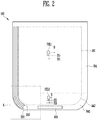
- FIG. 1 is a diagram illustrating a substrate 100 according to an embodiment of the present invention.
- the substrate 100 may include pixel areas AA1 and AA2 and peripheral areas NA1 and NA2.
- a plurality of pixels PXL1 and PXL2 may be located in the pixel areas AA1 and AA2 so that an image may be displayed on the pixel areas AA1 and AA2. Therefore, the pixel areas AA1 and AA2 may be referred to as a display area.
- Components such as drivers or wiring lines, for driving the pixels PXL1 and PXL2 may be located in the peripheral areas NA1 and NA2. Since the pixels PXL1 and PXL2 are not present in the peripheral areas NA1 and NA2, the peripheral areas NA1 and NA2 may be referred to as a non-display area.
- peripheral areas NA1 and NA2 may exist on the outside of the pixel areas AA1 and AA2 and surround at least portions of the pixel areas AA1 and AA2.
- the pixel areas AA1 and AA2 may include a first pixel area AA1 and a second pixel area AA2 located at one side of the first pixel area AA1.
- the first pixel area AA1 may have a greater area than the second area AA2.
- the peripheral areas NA1 and NA2 may include a first peripheral area NA1 and a second peripheral area NA2.
- the first peripheral area NA1 may be near the first pixel area AA1 and surround at least a portion of the first pixel area AA1.
- the second peripheral area NA2 may be near the second pixel area AA2 and surround at least a portion of the second pixel area AA2.
- the pixels PXL1 and PXL2 may include first pixels PXL1 and second pixels PXL2.
- the first pixels PXL1 may be located in the first pixel area AA1
- the second pixels PXL2 may be located in the second pixel area AA2.
- the pixels PXL1 and PXL2 may emit light with a predetermined brightness in response to control of drivers located in the peripheral areas NA1 and NA2.
- the pixels PXL1 and PXL2 may include organic light emitting diodes.
- the substrate 100 may have various shapes such that the above-described pixel areas AA1 and AA2 and peripheral areas NA1 and NA2 may be set.
- the substrate 100 may include two square corners and two rounded corners.
- the substrate 100 may include four rounded corners such that upper rounded corners and lower rounded corners may have different curvatures.
- a lower corner portion of the substrate 100 which corresponds to the second peripheral area NA2 and the second pixel area AA2 may have a curved shape with a predetermined curvature.
- the lower conrer portion of the substrate 100 may also have various shapes such as an angular shape.
- the second pixels PXL2 located in the second pixel area AA2 may be arranged in a different manner from the first pixels PXL1 located in the first pixel area AA1.
- the arrangement of the second pixels PXL2 will be described below.
- the substrate 100 may include an insulating material such as glass or resin.
- the substrate 100 may include a material with flexibility so that the substrate 100 may be bent or folded.
- the substrate 100 may have a single layer structure or a multilayer structure.
- the substrate 100 may include at least one of polystyrene, polyvinyl alcohol, polymethyl methacrylate, polyethersulfone, polyacrylate, polyetherimide, polyethylene naphthalate, polyethylene terephthalate, polyphenylene sulfide, polyarylate, polyimide, polycarbonate, triacetate cellulose, and cellulose acetate propionate.
- the substrate 100 may include various materials in addition to the above materials.
- the substrate 100 may include fiber glass reinforced plastic (FRP).
- FRP fiber glass reinforced plastic
- FIG. 2 is a diagram illustrating an organic light emitting display device according to an embodiment of the present invention.
- an organic light emitting display device may include the substrate 100, the first pixels PXL1, the second pixels PXL2, a scan driver 210, a light emitting driver 310, and a data driver 400.
- the first pixels PXL1 may be located in the first pixel area AA1. Each of the first pixels PXL1 may be connected to a first scan line S1i, a first light emission control line E1i, and a data line D.
- the second pixels PXL2 may be located in the second pixel area AA2. Each of the second pixels PXL2 may be connected to a second scan line S2i, a second light emission control line E2i, and the data line D.
- i is a natural number.
- reference character S1i may refer to an ith first scan line, among plural first scan lines.
- the scan driver 210 may supply scan signals to first scan lines S1i and second scan lines S2i. In other words, the scan driver 210 may drive the first pixels PXL1 and the second pixels PXL2. The scan driver 210 may be located in the first peripheral area NA1 and the second peripheral area NA2.
- the scan driver 210 may have a curved shape in the second peripheral area NA2 to correspond to the shape of the corner portion of the second peripheral area NA2 where it is disposed.
- the light emitting driver 310 may supply a light emission control signal to the first light emission control line E1i and the second light emission control line E2i. In other words, the light emitting driver 310 may drive the first pixels PXL1 and the second pixels PXL2. The light emitting driver 310 may be located in the first peripheral area NA1 and the second peripheral area NA2.
- the light emitting driver 310 may have a curved shape in the second peripheral area NA2 to correspond to the shape of the corner portion of the second peripheral area NA2 where it is disposed.
- FIG. 2 illustrates the light emitting driver 310 may be located separate the scan driver 210.
- the present invention is not limited thereto.
- the light emitting driver 310 may be combined with the scan driver 210 in a singular device.
- the data driver 400 may supply data signals to the first and second pixels PXL1 and PXL2 through the data lines D.
- a timing controller configured to supply predetermined control signals to the scan driver 210, the light emitting driver 310, and the data driver 400 may further be included.
- FIG. 3 is a detailed diagram illustrating an organic light emitting display device according to an embodiment of the present inventive concept.
- an organic light-emitting display device may include the scan driver 210, the light emitting driver 310, the data driver 400, a timing controller 180, the first pixels PXL1, and the second pixels PXL2.
- the first pixels PXL1 may be located in the first pixel area AA1 divided by first scan lines S11, S12,..., first light emission control lines E11, E12,..., and data lines D1 to Dm.
- the first pixels PXL1 may receive data signals from the data lines D1 to Dm when scan signals are supplied from the first scan lines S11, S12,....
- the first pixels PXL1 receiving the data signals may control the amount of current flowing from a first power supply ELVDD to a second power supply ELVSS via an organic light emitting diode.
- the second pixels PXL2 may be located in the second pixel area AA2 divided by second scan lines S21,..., second light emission control lines E21,..., and the data lines D1 to Dm.
- the second pixels PXL2 may receive data signals from the data lines D1 to Dm when scan signals are supplied from the second scan lines S21,....
- the second pixels PXL2 receiving the data signals may control the amount of current flowing from the first power supply ELVDD to the second power supply ELVSS via the organic light emitting diode.
- FIG. 3 illustrates the second pixels PXL2 arranged in a single pixel row.
- the present invention is not limited thereto.
- the second pixels PXL2 may be arranged in different rows, so that a plurality of the second scan lines S2i and a plurality of the second light emission control lines E2i may be formed.
- the scan driver 210 may supply scan signals to the first scan lines S11, S12,..., and the second scan lines S21,... in response to a first gate control signal GCS1 from the timing controller 180. For example, the scan driver 210 may sequentially supply scan signals to the first scan lines S11, S12,..., and the second scan lines S21,.... When the scan signals are sequentially supplied to the first scan lines S11, S12,..., and the second scan lines S21,..., the first pixels PXL1 and the second pixels PXL2 may be sequentially selected in units of horizontal lines.
- the scan driver 210 may be mounted onto the substrate 100 through a thin film process. In addition, the scan driver 210 may be mounted on both sides of the substrate 100 with the first pixel area AA1 and the second pixel area AA2 interposed therebetween.
- the light emitting driver 310 may supply light emission control signals to the first light emission control lines E11, E12,... and the second light emission control lines E21,... in response to a second gate control signal GCS2 from the timing controller 180. For example, the light emitting driver 310 may sequentially supply the light emission control signals to the first light emission control lines E11, E12,... and the second light emission control lines E21,....
- the light emission control signals may be used to control light emission times of the pixels PXL.
- PXL may be used to refer to at least one of the pixels PXL1 and PXL2.
- a light emission control signal may be set to have a greater width than a scan signal.
- the light emission control signals may be set to a gate off voltage (e.g., a high voltage) so that transistors included in the pixels PXL1 and PXL2 may be turned off, and the scan signals may be set to a gate on voltage (e.g., a low voltage) so that the transistors included in the pixels PXL1 and PXL2 may be turned on.
- a gate off voltage e.g., a high voltage
- the scan signals may be set to a gate on voltage (e.g., a low voltage) so that the transistors included in the pixels PXL1 and PXL2 may be turned on.
- the data driver 400 may supply data signals to the data lines D1 to Dm in response to a data control signal DCS.
- the data signals supplied to the data lines D1 to Dm may be supplied to the pixels PXL1 and PXL2 selected by the scan signals.
- FIG. 3 illustrates the data driver 400 located below the first pixel area AA1.
- the present invention is not limited thereto.
- the data driver 400 may be located above the first pixel area AA1.
- the timing controller 180 may supply the gate control signals GCS1 and GCS2, which are generated on the basis of externally supplied timing signals, to the scan driver 210 and the light emitting driver 310, and supply the data control signal DCS to the data driver 400.
- Each of the gate control signals GCS1 and GCS2 may include a start pulse and clock signals.
- the start pulse may control the timing of the first scan signal or the first light emission control signal.
- the clock signals may be used to shift the start pulse.
- the data control signal DCS may include a source start pulse and clock signals.
- the source start pulse may control a sampling start point of data.
- the clock signals may be used to control a sampling operation.
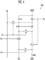
- FIG. 4 is a diagram illustrating a first pixel shown in FIG. 3 according to an embodiment of the present invention.
- FIG. 4 illustrates a first pixel coupled to an mth data line Dm and the ith first scan line S1i.
- the first pixel PXL1 may include an organic light emitting diode OLED, first to seventh transistors T1 to T7, and a storage capacitor Cst.
- An anode of the organic light emitting diode OLED may be coupled to the first transistor T1 through the sixth transistor T6, and a cathode thereof may be coupled to the second power supply ELVSS.
- the organic light emitting diode OLED may generate light with a predetermined brightness in response to the amount of current supplied from the first transistor T1.
- the first power supply ELVDD may be set to a greater voltage than the second power supply ELVSS so that a current may flow through the organic light emitting diode OLED.
- the seventh transistor T7 may be coupled between an initialization power supply Vint and the anode of the organic light emitting diode OLED.
- a gate electrode of the seventh transistor T7 may be coupled to an (i+1)th first scan line S1i+1.
- the seventh transistor T7 may be turned on when a scan signal is supplied to the (i+1)th first scan line S1i+1 to supply a voltage of the initialization power supply Vint to the organic light emitting diode OLED.
- the initialization power supply Vint may be set to have a lower voltage than a data signal.
- the sixth transistor T6 may be coupled between the first transistor T1 and the organic light emitting diode OLED.
- a gate electrode of the sixth transistor T6 may be coupled to the ith first light emission control line E1i.
- the sixth transistor T6 may be turned off when a light emission control signal is supplied to the ith first light emission control line E1i, and may be turned on when the light emission control signal is not supplied to the ith first light emission control line E1i.
- the fifth transistor T5 may be coupled between the first power supply ELVDD and the first transistor T1.
- a gate electrode of the fifth transistor T5 may be coupled to the ith first light emission control line E1i.
- the fifth transistor T5 may be turned off when the light emission control signal is supplied to the ith first light emission control line E1i, and may be turned on when the light emission control signal is not supplied to the ith first light emission control line E1i.
- a first electrode of the first transistor T1 (e.g., a driving transistor) may be coupled to the first power supply ELVDD through the fifth transistor T5, and a second electrode of the first transistor T1 may be coupled to the anode of the organic light emitting diode OLED via the sixth transistor T6.
- the gate electrode of the first transistor T1 may be coupled to a tenth node N10.
- the first transistor T1 may control the amount of current flowing from the first power supply ELVDD to the second power supply ELVSS via the organic light emitting diode OLED in response to a voltage of the tenth node N10.
- the third transistor T3 may be coupled between the second electrode of the first transistor T1 and the tenth node N10.
- a gate electrode of the third transistor T3 may be coupled to the ith first scan line S1i.
- the third transistor T3 may be turned on when the scan signal is supplied to the ith first scan line S1i to electrically connect the second electrode of the first transistor T1 to the tenth node N10. Therefore, when the third transistor T3 is turned on, the first transistor T1 may be connected in the form of a diode.
- the fourth transistor T4 may be coupled between the tenth node N10 and the initialization power supply Vint.
- a gate electrode of the fourth transistor T4 may be coupled to the (i-1)th first scan line S1i-1.
- the fourth transistor T4 may be turned on when a scan signal is supplied to the (i-1)th first scan line S1i-1 to supply a voltage of the initialization power supply Vint to the tenth node N10.
- the second transistor T2 may be coupled between the mth data line Dm and the first electrode of the first transistor T1.
- a gate electrode of the second transistor T2 may be coupled to the ith first scan line S1i.
- the second transistor T2 When the scan signal is supplied to the ith first scan line S1i, the second transistor T2 may be turned on to electrically connect the mth data line Dm to the first electrode of the first transistor T1.
- the storage capacitor Cst may be coupled between the first power supply ELVDD and the tenth node N10.
- the storage capacitor Cst may store voltages corresponding to a data signal and a threshold voltage of the first transistor T1.
- the second pixel PXL2 may have substantially the same circuit configuration as the first pixel PXL1. Therefore, a detailed description of the second pixel PXL2 will be omitted.
- FIG. 5 is a diagram illustrating a scan driver according to an embodiment of the present invention. For convenience of explanation, FIG. 5 illustrates four scan stages.
- the scan driver 210 may include a plurality of scan stages SST1 to SST4.
- Each of the scan stages SST1 to SST4 may be connected to one of the first scan lines S11 to S14 and be driven in response to first and second clock signals CLK1 and CLK2.
- the scan stages SST1 to SST4 may have the same circuit configuration.
- Each of the scan stages SST1 to SST4 may include first to third input terminals 1001 to 1003 and an output terminal 1004.
- the first input terminal 1001 of each of the scan stages SST1 to SST4 may receive an output signal (e.g., a scan signal) from a previous scan stage, or a first start pulse SSP1.
- the first input terminal 1001 of the first scan stage SST1 may receive the first start pulse SSP1
- the first input terminal 1001 of each of the scan stages SST2 to SST4 may receive an output signal from a previous scan stage.
- the second input terminal 1002 of a jth scan stage SSTj may receive the first clock signal CLK1, where j is an odd or even number.
- the third input terminal 1003 of the jth scan stage SSTj may receive the second clock signal CLK2.
- the second input terminal 1002 of a (j+1)th scan stage SSTj+1 may receive the second clock signal CLK2, and the third input terminal 1003 of the (j+1)th scan stage SSTj+1 may receive the first clock signal CLK1.
- the first clock signal CLK1 and the second clock signal CLK2 may have the same period and phases as each other may not overlap with each other. For example, when a period during which a scan signal is supplied to the first scan line S1i is a single horizontal period 1H, the clock signals CLK1 and CLK2 may each have a period of 2H and be supplied during different horizontal periods.
- each of the scan stages SST1 to SST4 may receive a first power supply VDD and a second power supply VSS.
- the first power supply VDD may be set to a gate off voltage, e.g., a high voltage
- the second power supply VSS may be set to a gate on voltage, e.g., a low voltage.
- FIG. 6 is a circuit diagram illustrating a scan stage shown in FIG. 5 according to an embodiment of the present invention. For convenience of explanation, FIG. 6 illustrates the first scan stage SST1 and and the second scan stage SST2.
- the first scan stage SST1 may include a first driver 1210, a second driver 1220, an output unit 1230 (or a buffer), and a first transistor M1.
- the output unit 1230 may control a voltage supplied to the output terminal 1004 in response to voltages of a first node N1 and a second node N2.
- the output unit 1230 may include a fifth transistor M5 and a sixth transistor M6.
- the fifth transistor M5 may be located between the first power supply VDD and the output terminal 1004 and have a gate electrode connected to the first node N1.
- the fifth transistor M5 may control the connection between the first power supply VDD and the output terminal 1004 in response to a voltage applied to the first node N1.
- the sixth transistor M6 may be located between the output terminal 1004 and the third input terminal 1003 and have a gate electrode coupled to the second node N2.
- the sixth transistor M6 may control the connection between the output terminal 1004 and the third input terminal 1003 in response to a voltage applied to the second node N2.
- the output unit 1230 may be driven as a buffer.
- the fifth transistor M5, and/or the sixth transistor M6 may be composed of a plurality of transistors connected in parallel with each other.
- the first driver 1210 may control a voltage of a third node N3 in response to signals supplied to the first to third input terminals 1001 to 1003.
- the first driver 1210 may include second to fourth transistors M2 to M4.
- the second transistor M2 may be interposed between the first input terminal 1001 and a third node N3, and a gate electrode of the second transistor M2 may be coupled to the second input terminal 1002.
- the second transistor M2 may control the connection between the first input terminal 1001 and the third node N3 in response to the signals supplied to the second input terminal 1002.
- the third transistor M3 and the fourth transistor M4 may be connected in series between the third node N3 and the first power supply VDD.
- the third transistor M3 may be located between the fourth transistor M4 and the third node N3 and a gate electrode of the third transistor M3 may be coupled to the third input terminal 1003.
- the third transistor M3 may control the connection between the fourth transistor M4 and the third node N3 in response to the signals supplied to the third input terminal 1003.
- the fourth transistor M4 may be located between the third transistor M3 and the first power supply VDD and a gate electrode of the fourth transistor M4 may be coupled to the first node N1.
- the fourth transistor M4 may control the connection between the third transistor M3 and the first power supply VDD in response to the voltage of the first node N1.
- the second driver 1220 may control the voltage of the first node N1 in response to voltages of the second input terminal 1002 and the third node N3.
- the second driver 1220 may include a seventh transistor M7, an eighth transistor M8, a first capacitor C1, and a second capacitor C2.
- the first capacitor C1 may be coupled between the second node N2 and the output terminal 1004.
- the first capacitor C1 may be charged with voltages corresponding to a turn-on state and a turn-off state of the sixth transistor M6.
- the second capacitor C2 may be coupled between the first node N1 and the first power supply VDD.
- the second capacitor C2 may be charged with the voltage applied to the first node N1.
- the seventh transistor M7 may be located between the first node N1 and the second input terminal 1002 and a gate electrode of the seventh transistor M7 may be coupled to the third node N3.
- the seventh transistor M7 may control the connection between the first node N1 and the second input terminal 1002 in response to the voltage of the third node N3.
- the eighth transistor M8 may be located between the first node N1 and the second power supply VSS and a gate electrode of the eighth transistor M8 may be coupled to the second input terminal 1002.
- the eighth transistor M8 may control the connection between the first node N1 and the second power supply VSS in response to a signal from the second input terminal 1002.
- the first transistor M1 may be located between the third node N3 and the second node N2 and a gate electrode of the first transistor M1 may be coupled to the second power supply VSS.
- the first transistor M1 may maintain a turn-on state and maintain the electrical connection between the third node N3 and the second node N2.
- the first transistor M1 may limit a width by which the voltage of the third node N3 is lowered in response to the voltage of the second node N2. In other words, when the voltage of the second node N2 is lowered to a voltage less than the second power supply VSS, the voltage of the third node N3 may not be reduced to a voltage obtained by subtracting a threshold voltage of the first transistor M1 from the second power supply VSS. A detailed description thereof will be described below.
- FIG. 7 is a waveform diagram illustrating a method of driving a scan stage shown in FIG. 6 according to an embodiment of the present invention. For convenience of explanation, FIG. 7 illustrates operations using the first scan stage SST1.
- each of the first clock signal CLK1 and the second clock signal CLK2 may have two horizontal periods (2H).
- the first and second clock signals CLK1 and CLK2 may be supplied during different horizontal periods.
- the second clock signal CLK2 may be set to a signal shifted by a half period, e.g., a single horizontal period, from the first clock signal CLK1.
- the first start pulse SSP1 supplied to the first input terminal 1001 may be supplied in synchronization with a clock signal supplied to the second input terminal 1002, e.g., the first clock signal CLK1.
- the first input terminal 1001 when the first start pulse SSP1 is supplied, the first input terminal 1001 may be set to a voltage of the second power supply VSS. When the first start pulse SSP1 is not supplied, the first input terminal 1001 may be set to a voltage of the first power supply VDD. In addition, when the clock signal CLK is supplied to the second input terminal 1002 and the third input terminal 1003, the second input terminal 1002 and the third input terminal 1003 may be set to the voltage of the second power supply VSS. When the clock signal CLK is not supplied to the second input terminal 1002 and the third input terminal 1003, the second input terminal 1002 and the third input terminal 1003 may be set to the voltage of the first power supply VDD.
- the first start pulse SSP1 may be supplied in synchronization with the first clock signal CLK1.
- the second transistor M2 and the eighth transistor M8 may be turned on.
- the first input terminal 1001 and the third node N3 may be electrically connected to each other. Since the first transistor M1 is set to a turn-on state at all times, the second node N2 may maintain an electrical connection with the third node N3.
- the third node N3 and the second node N2 may be set to a low voltage by the first start pulse SSP1 supplied to the first input terminal 1001.
- the sixth transistor M6 and the seventh transistor M7 may be turned on.
- the third input terminal 1003 and the output terminal 1004 may be electrically connected to each other.
- the third input terminal 1003 may be set to a high voltage (e.g., when the second clock signal CLK2 is not supplied to the third input terminal 1003). Therefore, the high voltage may also be output to the output terminal 1004.
- the seventh transistor M7 When the seventh transistor M7 is turned on, the second input terminal 1002 and the first node N1 may be electrically connected to each other.
- a voltage of the first clock signal CLK1 supplied to the second input terminal 1002, e.g., a low voltage, may be supplied to the first node N1.
- the eighth transistor M8 when the first clock signal CLK1 is supplied, the eighth transistor M8 may be turned on.
- the voltage of the second power supply VSS may be supplied to the first node N1.
- the voltage of the second power supply VSS may be set to the same (or similar) voltage as the first clock signal CLK1, so that the first node N1 may stably maintain the low voltage.
- the fourth transistor M4 and the fifth transistor M5 may be turned on.
- the fourth transistor M4 When the fourth transistor M4 is turned on, the first power supply VDD and the third transistor M3 may be electrically connected to each other. Since the third transistor M3 is set to a turn-off state, the third node N3 may stably maintain the low voltage when the fourth transistor M4 is turned on.
- the fifth transistor M5 When the fifth transistor M5 is turned on, the voltage of the first power supply VDD may be applied to the output terminal 1004.
- the voltage of the first power supply VDD may be set to the same voltage as the high voltage of the third input terminal 1003. Therefore, the output terminal 1004 may stably maintain the high voltage.
- the supply of the first start pulse SSP1 and the first clock signal CLK1 may be stopped.
- the second transistor M2 and the eighth transistor M8 may be turned off.
- the sixth transistor M6 and the seventh transistor M7 may maintain the turn-on state in response to the voltages stored in the first capacitor C1.
- the second node N2 and the third node N3 may maintain the low voltages by virtue of the voltages stored in the first capacitor C 1.
- the output terminal 1004 and the third input terminal 1003 may maintain their electrical connection.
- the seventh transistor M7 maintains the turn-on state
- the first node N1 may maintain the electrical connection with the second input terminal 1002.
- a voltage of the second input terminal 1002 may be set to a high voltage in response to an interruption of the supply of the first clock signal CLK1, and the first node N1 may also be set to the high voltage.
- the fourth transistor M4 and the fifth transistor M5 may be turned off.
- the second clock signal CLK2 may be supplied to the third input terminal 1003. Since the sixth transistor M6 is set to the turn-on state, the second clock signal CLK2 supplied to the third input terminal 1003 may be supplied to the output terminal 1004. The output terminal 1004 may output the second clock signal CLK2 as a scan signal to the first scan line S11.
- the voltage of the second node N2 may be lowered to a voltage less than the second power supply VSS by coupling of the first capacitor C1, so that the sixth transistor M6 may stably maintain a turn-on state.
- the third node N3 may maintain the voltage of the second power supply VSS (e.g., the maintained voltage may be a voltage obtained by subtracting the threshold voltage of the first transistor M1 from the second power supply VSS) by virtue of the first transistor M1.
- the supply of the second clock signal CLK2 may be stopped.
- the output terminal 1004 may output a high voltage.
- the voltage of the second node N2 may be increased to approximately the voltage of the second power supply VSS in response to the high voltage of the output terminal 1004.
- the first clock signal CLK1 may be supplied.
- the second transistor M2 and the eighth transistor M8 may be turned on.
- the first input terminal 1001 and the third node N3 may be electrically connected to each other. Since the first start pulse SSP1 is not supplied to the first input terminal 1001, the first input terminal 1001 may be set to a high voltage. Therefore, when the first transistor M1 is turned on, the high voltage may be supplied to the third node N3 and the second node N2, so that the sixth transistor M6 and the seventh transistor M7 may be turned off.
- the second power supply VSS may be supplied to the first node N1, so that the fourth transistor M4 and the fifth transistor M5 may be turned on.
- the fifth transistor M5 When the fifth transistor M5 is turned on, the voltage of the first power supply VDD may be supplied to the output terminal 1004. Subsequently, the fourth transistor M4 and the fifth transistor M5 may maintain the turn-on state in response to the voltage charged in the second capacitor C2, so that output terminal 1004 may stably receive the voltage of the first power supply VDD.
- the third transistor M3 may be turned on. Since the fourth transistor M4 is set to the turn-on state, the voltage of the first power supply VDD may be supplied to the third node N3 and the second node N2. The sixth transistor M6 and the seventh transistor M7 may stably maintain the turn-off state.
- the second scan stage SST2 may receive an output signal (e.g., a scan signal) from the first scan stage SST1 to be synchronized with the second clock signal CLK2.
- the second scan stage SST2 may output a scan signal to the second scan line S12 to be synchronized with the first clock signal CLK1.
- the scan stages SST of the present invention may repeat the above-described operations and sequentially output scan signals to the scan lines.
- the first transistor M1 may limit the minimum voltage width of the third node N3 regardless of the voltage of the second node N2, so that manufacturing costs and driving reliability may be ensured.
- the voltage of the second node N2 may be lowered to a voltage of approximately VSS - (VDD - VSS).
- VDD voltage of approximately VSS -
- the voltage of the second node N2 may be lowered to approximately -20V despite threshold voltages of the transistors.
- Vds of the second transistor M2 and Vgs of the seventh transistor M7 may be set to approximately -27V. Therefore, components having a high internal pressure may be used as the second transistor M2 and the seventh transistor M7. In addition, when a high voltage is applied to the second transistor M2 and the seventh transistor M7, a large amount of power may be consumed and driving reliability may be lowered. However, according to an exemplary embodiment of the present invention, when the first transistor M1 is added between the third node N3 and the second node N2, the voltage of the third node N3 may be maintained at a voltage of approximately the second power supply VSS. As a result, Vds of the second transistor M2 and Vgs of the seventh transistor M7 may be set to approximately -14V.
- Scan stages may also be provided in the second peripheral area NA2 as well as the first peripheral area NA1.
- the scan stages provided in the second peripheral area NA2 may be configured in substantially the same manner and drive by substantially the same driving method as the above-described scan stages
- FIG. 8 is a diagram illustrating a light emitting driver according to an embodiment of the present invention. For convenience of explanation, FIG. 8 illustrates four light emitting stages.
- the light emitting driver 310 may include a plurality of light emitting stages EST1 to EST4. Each of the light emitting stages EST1 to EST4 may be coupled to one of the first light emission control lines E11 to E14 and be driven by third and fourth clock signals CLK3 and CLK4. The light emitting stages EST1 to EST4 may be realized with the same circuit configurations as each other.
- Each of the light emitting stages EST1 to EST4 may include first to third input terminals 2001 to 2003 and an output terminal 2004.
- the first input terminal 2001 of each of the light emitting stages EST1 to EST4 may receive an output signal (e.g., a light emission control signal) from a previous light emitting stage, or a second start pulse SSP2.
- an output signal e.g., a light emission control signal
- the first input terminal 2001 of the first light emitting stage EST1 may receive the second start pulse SSP2 and the first input terminal 2001 of each of the remaining light emitting stages EST2 to EST4 may receive an output signal of a previous stage.
- the second input terminal 2002 of a jth light emitting stage ESTj may receive the third clock signal CLK3, and the third input terminal 2003 of the jth light emitting stage ESTj may receive the fourth clock signal CLK4.
- the second input terminal 2002 of a (j+1)th light emitting stage ESTj+1 may receive the fourth clock signal CLK4, and the third input terminal 2003 of the (j+1)th light emitting stage ESTj+1 may receive the third clock signal CLK3.
- the third clock signal CLK3 and the fourth clock signal CLK4 may have the same period and phases as each other may not overlap with each other.
- the clock signals CLK3 and CLK4 may each have a period of 2H and be supplied during different horizontal periods.
- each of the light emitting stages EST1 to EST4 may receive a third power supply VDD1 and a fourth power supply VSS1.
- the third power supply VDD 1 may be set as a gate off voltage and the fourth power supply VSS1 may be set as a gate on voltage.
- the third power supply VDD1 may be set to the same voltage as the first power supply VDD, and the fourth power supply VSS1 may be set to the same voltage as the second power supply VSS.
- FIG. 9 is a circuit diagram illustrating a light emitting stage shown in FIG. 8 according to an embodiment of the present invention. For convenience of explanation, FIG. 9 illustrates the first light emitting stage EST1 and the second light emitting stage EST2.
- the first light emitting stage EST1 may include a first signal processor 2100, a second signal processor 2200, a third signal processor 2300, and an output unit 2400 (or buffer).
- the first signal processor 2100 may control voltages of a twenty-second node N22 and a twenty-first node N21 in response to signals supplied to the first input terminal 2001 and the second input terminal 2002.
- the first signal processor 2100 may include an eleventh transistor M11, a twelfth transistor M12, and a thirteenth transistor M13.
- the eleventh transistor M11 may be located between the first input terminal 2001 and the twenty-first node N21 and a gate electrode of the eleventh transistor M11 may be coupled to the second input terminal 2002.
- the eleventh transistor M11 may be turned on when the third clock signal CLK3 is supplied to the second input terminal 2002.
- the twelfth transistor M12 may be located between the second input terminal 2002 and the twenty-second node N22 and a gate electrode of the twelfth transistor M12 may be coupled to the twenty-first node N21.
- the twelfth transistor M12 may be turned on or off in response to a voltage of the twenty-first node N21.
- the thirteenth transistor M13 may be located between the fourth power supply VSS1 and the twenty-second node N22 and a gate electrode of the thirteenth transistor M13 may be coupled to the second input terminal 2002.
- the thirteenth transistor M13 may be turned on when the third clock signal CLK3 is supplied to the second input terminal 2002.
- the second signal processor 2200 may control voltages of the twenty-first node N21 and a twenty-third node N23 in response to the signals supplied to the third input terminal 2003 and a voltage of the twenty-second node N22.
- the second signal processor 2200 may include fourteenth to seventeenth transistors M14 to M17, an eleventh capacitor C11, and a twelfth capacitor C12.
- the fourteenth transistor M14 may be located between the fifteenth transistor M15 and the twenty-first node N21 and a gate electrode of the fourteenth transistor M14 may be coupled to the third input terminal 2003.
- the fourteenth transistor M14 may be turned on when the fourth clock signal CLK4 is supplied to the third input terminal 2003.
- the fifteenth transistor M15 may be located between the third power supply VDD1 and the fourteenth transistor M14 and a gate electrode of the fifteenth transistor M15 may be coupled to the twenty-second node N22.
- the fifteenth transistor M15 may be turned on or off in response to the voltage of the twenty-second node N22.
- the sixteenth transistor M16 may be located between a first electrode of the seventeenth transistor M17 and the third input terminal 2003 and a gate electrode of the sixteenth transistor M16 may be coupled to the twenty-second node N22.
- the sixteenth transistor M16 may be turned on or off in response to the voltage of the twenty-second node N22.
- the seventeenth transistor M17 may be located between a first electrode of the sixteenth transistor M16 and the twenty-third node N23 and a gate electrode of the seventeenth transistor M17 may be coupled to the third input terminal 2003.
- the seventeenth transistor M17 may be turned on when the fourth clock signal CLK4 is supplied to the third input terminal 2003.
- the eleventh capacitor C11 may be coupled between the twenty-first node N21 and the third input terminal 2003.
- the twelfth capacitor C12 may be coupled between the twenty-second node N22 and the first electrode of the seventeenth transistor M17.
- the third signal processor 2300 may control a voltage of the twenty-third node N23 in response to the voltage of the twenty-first node N21.
- the third signal processor 2300 may include an eighteenth transistor M18 and a thirteenth capacitor C13.
- the eighteenth transistor M18 may be located between the third power supply VDD1 and the twenty-third node N23 and a gate electrode of the eighteenth transistor M18 may be coupled to the twenty-first node N21.
- the eighteenth transistor M18 may be turned on or off in response to the voltage of the twenty-first node N21.
- the thirteenth capacitor C13 may be located between the third power supply VDD1 and the twenty-third node N23.
- the output unit 2400 may control a voltage supplied to the output terminal 2004 in response to the voltages of the twenty-first node N21 and the twenty-third node N23.
- the output unit 2400 may include a nineteenth transistor M19 and a twentieth transistor M20.
- the nineteenth transistor M19 may be located between the third power supply VDD1 and the output terminal 2004 and a gate electrode of the nineteenth transistor M19 may be coupled to the twenty-third node N23.
- the nineteenth transistor M19 may be turned on or off in response to the voltage of the twenty-third node N23.
- the twentieth transistor M20 may be located between the output terminal 2004 and the fourth power supply VSS1 and a gate electrode of the twentieth transistor M20 may be coupled to the twenty-first node N21.
- the twentieth transistor M20 may be turned on or off in response to the voltage of the twenty-first node N21.
- the output unit 2400 may be driven as a buffer.
- the nineteenth transistor M19 and/or the twentieth transistor M20 may be composed of a plurality of transistors connected in parallel.
- FIG. 10 is a waveform diagram illustrating a method of driving light emitting stages shown in FIG. 9 according to an embodiment of the present invention. For convenience of explanation, FIG. 10 illustrates operations using the first light emitting stage EST1.
- the third clock signal CLK3 and the fourth clock signal CLK4 may each have two horizontal periods 2H and be supplied during different horizontal periods.
- the fourth clock signal CLK4 may be set to a signal shifted by a half period (e.g., a single horizontal period 1H) from the third clock signal CLK3.
- the first input terminal 2001 When the second start pulse SSP2 is supplied, the first input terminal 2001 may be set to a voltage of the third power supply VDD1. When the second start pulse SSP2 is not supplied, the first input terminal 2001 may be set to a voltage of the fourth power supply VSS1. In addition, when the clock signal CLK is supplied to the second input terminal 2002 and the third input terminal 2003, the second input terminal 2002 and the third input terminal 2003 may be set to the voltage of the fourth power supply VSS1. When the clock signal CLK is not supplied to the second input terminal 2002 and the third input terminal 2003, the second input terminal 2002 and the third input terminal 2003 may be set to the voltage of the third power supply VDD1.
- the second start pulse SSP2 supplied to the first input terminal 2001 may be supplied in synchronization with the clock signal supplied to the second input terminal 2002, e.g., the third clock signal CLK3.
- the second start pulse SSP2 may be set to have a greater width than the third clock signal CLK3.
- the second start pulse SSP2 may be supplied during four horizontal periods 4H.
- the third clock signal CLK3 may be supplied to the second input terminal 2002 during a first time t1.
- the eleventh transistor M11 and the thirteenth transistor M13 may be turned on.
- the eleventh transistor M11 When the eleventh transistor M11 is turned on, the first input terminal 2001 and the twenty-first node N21 may be electrically connected to each other. Since the second start pulse SSP2 is not supplied to the first input terminal 2001, a low voltage may be supplied to the twenty-first node N21.
- the twelfth transistor M12, the eighteenth transistor M18 and the twentieth transistor M20 may be turned on.
- the third power supply VDD1 may be supplied to the twenty-third node N23, so that the nineteenth transistor M19 may be turned off.
- the thirteenth capacitor C13 may be charged with a voltage corresponding to the third power supply VDD1, so that the nineteenth transistor M19 may stably maintain the turn-off state after the first time t1.
- the voltage of the fourth power supply VSS1 may be supplied to the output terminal 2004. Therefore, during the first time t1, a light emission control signal may not be supplied to the first light emission control line E11.
- the third clock signal CLK3 may be supplied to the twenty-second node N22.
- the voltage of the fourth power supply VSS1 may be supplied to the twenty-second node N22.
- the third clock signal CLK3 may be set to the voltage of the fourth power supply VSS1, so that the twenty-second node N22 may be stably set to the voltage of the fourth power supply VSS1.
- the seventeenth transistor M17 may be set to a turn-off state. Therefore, the twenty-third node N23 may maintain a voltage of the third power supply VDD1 regardless of the voltage of the twenty-second node N22.
- the supply of the third clock signal CLK3 to the second input terminal 2002 may be stopped during a second time t2.
- the eleventh transistor M11 and the thirteenth transistor M13 may be turned off.
- the voltage of the twenty-first node N21 may be maintained at a low voltage by the eleventh capacitor C11, so that the twelfth transistor M12, the eighteenth transistor M18, and the twentieth transistor M20 may maintain the turn-on state.
- the second input terminal 2002 and the twenty-second node N22 may be electrically connected to each other.
- the twenty-second node N22 may be set to a high voltage.
- a voltage of the third power supply VDD1 may be supplied to the twenty-third node N23, so that the nineteenth transistor M19 may maintain the turn-off state.
- the voltage of the fourth power supply VSS1 may be supplied to the output terminal 2004.
- the fourth clock signal CLK4 may be supplied to the third input terminal 2003 during a third time t3.
- the fourteenth transistor M14 and the seventeenth transistor M17 may be turned on.
- the seventeenth transistor M17 When the seventeenth transistor M17 is turned on, the twelfth capacitor C12 and the twenty-third node N23 may be electrically connected to each other.
- the twenty-third node N23 may maintain the voltage of the third power supply VDD1.
- the fourteenth transistor M14 when the fourteenth transistor M14 is turned on, the fifteenth transistor M15 may be set to a turn-off state. Therefore, when the fourteenth transistor M14 is turned on, the voltage of the twenty-first node N21 may not be changed.
- the twenty-first node N21 may be reduced to a smaller voltage than the fourth power supply VSS1 by coupling of the eleventh capacitor C11.
- driving characteristics of the eighteenth transistor M18 and the twentieth transistor M20 may be increased since, e.g., a PMOS transistor has better driving characteristics when receiving a lower voltage level.
- the second start pulse SSP2 may be supplied to the first input terminal 2001 and the third clock signal CLK3 may be supplied to the second input terminal 2002.
- the eleventh transistor M11 and the thirteenth transistor M13 may be turned on.
- the eleventh transistor M11 When the eleventh transistor M11 is turned on, the first input terminal 2001 and the twenty-first node N21 may be electrically connected to each other. Since the second start pulse SSP2 is supplied to the first input terminal 2001, a high voltage may be supplied to the twenty-first node N21.
- the twelfth transistor M 12, the eighteenth transistor M18 and the twentieth transistor M20 may be turned off.
- the voltage of the fourth power supply VSS1 may be supplied to the twenty-second node N22. Since the fourteenth transistor M14 is set to the turn-off state, the twenty-first node N21 may maintain the high voltage. In addition, since the seventeenth transistor M17 is set to the turn-off state, the voltage of the twenty-third node N23 may maintain the high voltage of the thirteenth capacitor C13. Therefore, the nineteenth transistor M19 may maintain the turn-off state.
- the fourth clock signal CLK4 may be supplied to the third input terminal 2003 during a fifth time t5.
- the fourteenth transistor M14 and the seventeenth transistor M17 may be turned on.
- the twenty-second node N22 is set to the voltage of the fourth power supply VSS1, the fifteenth transistor M15 and the sixteenth transistor M16 may be turned on.
- the fourth clock signal CLK4 may be supplied to the twenty-third node N23.
- the nineteenth transistor M19 may be turned on.
- the voltage of the third power supply VDD1 may be supplied to the output terminal 2004.
- the voltage of the third power supply VDD1 supplied to the output terminal 2004 may be supplied as a light emission control signal to the first light emission control line E11.
- the voltage of the twenty-second node N22 may be lowered to a smaller voltage than the fourth power supply VSS1 by coupling of the twelfth capacitor C12, so that driving characteristics of the transistors coupled to the twenty-second node N22 may be increased.
- the voltage of the third power supply VDD1 may be supplied to the twenty-first node N21.
- the twentieth transistor M20 may maintain the turn-off state. Therefore, the voltage of the third power supply VDD1 may be stably supplied to the first light emission control line E11.
- the third clock signal CLK3 may be supplied to the second input terminal 2002 during a sixth time t6.
- the eleventh transistor M11 and the thirteenth transistor M13 may be turned on.
- the eleventh transistor M11 When the eleventh transistor M11 is turned on, the twenty-first node N21 and the first input terminal 2001 may be electrically connected to each other, so that the twenty-first node N21 may be set to a low voltage.
- the eighteenth transistor M18 and the twentieth transistor M20 When the twenty-first node N21 is set to the low voltage, the eighteenth transistor M18 and the twentieth transistor M20 may be turned on.
- the voltage of the third power supply VDD1 may be supplied to the twenty-third node N23, so that the nineteenth transistor M 19 may be turned off.
- the voltage of the fourth power supply VSS1 may be supplied to the output terminal 2004.
- the voltage of the fourth power supply VSS1 supplied to the output terminal 2004 may be supplied to the first light emission control line E11, so that the supply of the light emission control signal may be stopped.
- the light emitting stages EST may repeat the above-described processes to sequentially output light emission control signals to light emission control lines.
- transistors are illustrated as PMOS transistors.
- the present invention may not be limited thereto.
- the transistors may be NMOS transistors.
- Light emitting stages may also be provided in the second peripheral area NA2 as well as the first peripheral area NA1.
- the light emitting stages provided in the second peripheral area NA2 may have the same configuration as the above-described light emitting stages and be operated by the same driving method.
- the first light emitting stage in the second peripheral area NA2 may operate upon receiving an output signal from the last light emitting stage provided in the first peripheral area NA1.
- the organic light emitting diode OLED may generate light of various colors including red, green and blue in response to the amount of current supplied from the driving transistor.
- the present invention is not limited thereto.
- the organic light emitting diode OLED may generate white light in response to the amount of current supplied from the driving transistor.
- a color image may be displayed using a separate color filter.
- FIG. 11 is an enlarged diagram of a region A of an organic light-emitting display device shown in FIG. 2 according to an exemplary embodiment of the present invention.
- the region A illustrated in FIG. 2 may include some of the lower part of the first pixel area AA1 and some of the corner portion of the second pixel area AA2.
- the region A may include a portion of the first peripheral area NA1 and a portion of the second peripheral area NA2.
- the pixels PXL1 and PXL2 provided in the region A may include a plurality of pixel rows PR1 in which each of the pixels may extend in a first direction DR1.
- Each of the pixel rows PR1 may be arranged in a second direction DR2.
- pixel columns PC1 may be formed such that each of the pixels PXL1 and PXL2 may extend in the second direction DR2.
- Each of the pixel columns PC1 may be arranged in the first direction DR1.
- the pixels PXL1 and PXL2 may be arranged in a matrix format.
- the first pixel area AA1 may have a rectangular shape.
- outermost pixels of the respective pixel rows PR1 may have the same x-axis position
- each pixel row PR1 may have the same number of pixels
- each pixel row PR1 may have the same length in the first direction DR1.
- the pixel row PR1 closer to the first pixel area AA1 may have a larger number of pixels PXL2, and the pixel row PR1 closer to a lower part of the second pixel area AA2 may include a smaller number of second pixels PXL2.
- the x-axis position of the leftmost pixel of the pixel row PR1 in the first pixel area AA1 when used as a reference position, the x-axis position of the rightmost pixel may be more distant from the reference position as the pixel row PR1 in the second pixel area AA2 advances in the second direction DR2, and the number of pixels PXL2 constituting the pixel row PR1 may gradually decrease.
- a length L of the pixel row PR1 in the first direction DR1 may gradually decrease, so that the corner portion of the second pixel area AA2 may have a curved shape.
- FIG. 11 illustrates the second pixels PXL2 arranged in seven rows.
- the present invention is not limited thereto.
- the number of pixel rows PR1 forming the second pixel area AA2 may vary.
- first and second pixel areas AA1 and AA2 are illustrated. However, the left and right sides of the first and second pixel areas AA1 and AA2 may be symmetrical with respect to each other.
- the lengths of the pixel rows PR1 arranged in the second pixel area AA2 may gradually decrease as the pixel rows PR1 go down in the second direction DR2. However, the lengths are not necessarily reduced at the same rate (or the numbers of pixels PXL2 arranged in the pixel rows PR1 are not necessarily reduced at the same rate).
- the number of pixels PXL2 arranged in each pixel row PR1 may vary depending on the curvature of a curved line defining the corner portion of the second pixel area AA2.
- the first peripheral area NA1 and the second peripheral area NA2 may include first scan stages SST11 to SST13 and second scan stages SST21 to SST27, respectively.
- Each of the first scan stages SST11 to SST13 may correspond to each of the pixel rows PR1 included in the first pixel area AA1 and supply scan signals to the first pixels PXL1 arranged in a corresponding pixel row.
- a scan line S connecting an output terminal of each of the first scan stages SST11 to SST13 to a scan signal input terminal of the outermost pixel of the pixel row PR1 has a length SL1
- the scan lines S included in the first pixel area AA1 may have the same length SL1.
- a scan signal input terminal of a pixel may be included in a pixel circuit and refer to a gate electrode (e.g., the gate electrode of the transistor T2 shown in FIG. 4 ) of a predetermined transistor driven by a scan signal supplied through the scan line S.
- the scan lines S provided in the first pixel area AA1 may be in parallel with the first direction DR1.
- the output terminal of each of the first scan stages SST11 to SST13 and the scan signal input terminal of the outermost pixel in the pixel row PR1 may have the same position in the second direction DR2.
- Each of first light emitting stages EST11 to EST13 may be provided at one side of each of the first scan stages SST11 to SST13.
- Each of the first light emitting stages EST11 to EST13 may correspond to each of the pixel rows PR1 provided in the first pixel area AA1 and supply light emission control signals to the first pixels PXL1 arranged in the corresponding pixel row.
- the second scan stages SST21 to SST27 may be arranged in a curved shape to correspond to the shape of the corner of the second peripheral area NA2.
- some or all lines connecting the respective output terminals of the second scan stages SST21 to SST27 may be curved lines having predetermined curvatures.
- the length SL2 of each of the scan lines S included in the second pixel area AA2 may be greater than the length SL1 of each of the scan lines S included in the first pixel area AA1.
- the length SL2 of the scan line S closer to the first pixel area AA1 may be smaller and the length SL2 of the scan line S closer to the lower part of the second pixel area AA2 may be greater.
- the scan lines provided in the second pixel area AA2 may be formed at a predetermined angle (greater than zero degrees) with respect to the first direction DR1.
- the output terminal of each of the second scan stages SST21 to SST27 and the scan signal input terminal of the outermost pixel in the pixel row PR1 may have different positions in the second direction DR2, so that the scan line S may be connected at a predetermined slope.
- a y-axis output position of at least one of the second scan stages SST21 to SST27 may be arranged to be higher than a y-axis position of the scan signal input terminal of the second pixel PXL2 connected through the scan line S.
- each of the second scan stages SST21 to SST27 When the y-axis output position of each of the second scan stages SST21 to SST27 is located above the y-axis position of the scan signal input terminal of the second pixel PXL2 connected through the scan line S, a portion of each of the second scan stages SST21 to SST27 may be located below the y-axis position of the scan signal input terminal of the second pixel PXL2 corresponding thereto.
- the y-axis output position of at least one of the second scan stages SST21 to SST27 may be lower than the y-axis position of the scan signal input terminal of the second pixel PXL2 connected through the scan line S.
- the y-axis output position of each of the second scan stages SST21 to SST27 is lower than the y-axis position of the scan signal input terminal of the second pixel PXL2 corresponding thereto, a portion of each of the second scan stages SST21 to SST27 may be higher than the y-axis position of the scan signal input terminal of the second pixel PXL2 corresponding thereto.
- the scan signal input terminal of the pixel PXL1 or PXL2 may be provided in a pixel circuit and refer to a gate electrode (e.g., a gate electrode of the transistor T4 shown in FIG. 4 ) of a predetermined transistor driven by a scan signal supplied through the scan line S.
- a gate electrode e.g., a gate electrode of the transistor T4 shown in FIG. 4
- the scan lines S included in the second pixel area AA2 may have linear shapes having the same slope between the output terminals of the second scan stages SST21 to SST27 to the input terminals of the outermost pixels of the pixel rows PR1.
- the present invention is not limited thereto. In other words, as illustrated in FIG. 11 , each of the scan lines S may be curved at a predetermined position.
- Each of the second light emitting stages EST21 to EST27 may be provided at one side of each of the second scan stages SST21 to SST27.
- the second light emitting stages EST21 to EST27 may be arranged in a curved shape to correspond to the second peripheral area NA2.
- some or all lines connecting the respective output terminals of the second light emitting stages EST21 to EST27 may be curved lines having predetermined curvatures.
- Each of the second light emitting stages EST21 to EST27 may correspond to each of the pixel rows PR1 provided in the second pixel area AA2 and supply light emission control signals to the second pixels PXL2 arranged in the corresponding pixel row PR1.
- the data driver 400 may be provided at another side of the second pixel area AA2. For example, away from the curved side of the second pixel area AA2.
- a corresponding data line D may be connected to each of the pixel columns PC1.
- the same data line D may be connected to the first pixels PXL1 and the second pixels PXL2 arranged in the same pixel columns PC1.
- the scan lines S may be connected in the first direction DR1 and the data lines D may be connected in the second direction DR2.
- overlapping portions may exist between the scan lines S and the data lines D.
- the pixel row PR1 closer to the lower part of the second pixel area AA2 may include a smaller number of pixels PXL2 so that the corner portion of the second pixel area AA2 may be curved. Therefore, the number of data lines D passing through the sides of the second pixels PXL2 may increase toward the lower part of the second pixel area AA2. As a result, more overlapping may occur between the scan line S and the data line D in the pixel row PR1 closer to the lower part of the second pixel area AA2.
- FIG. 11 illustrates the structures of the second pixels PXL2 and the second scan stages SST21 to SST27 arranged in the second pixel area AA2 and the second peripheral area NA2 in detail.
- the arrangements of the components illustrated in FIG. 11 may be applicable to other components.
- the above-described configurations of the pixels, scan lines, the light emission control lines, the scan stages and the light emitting stages may be applicable to the corresponding portion.
- FIG. 12 is an enlarged view of some of the components of an organic light-emitting display device shown in FIG. 11 which are located in a second pixel area and a second peripheral area according to an embodiment of the present invention.
- FIG. 12 shows the second scan stage SST24 and the second scan stage SST27, among the second scan stages SST21 to SST27, the scan lines S coupled to the second scan stages SST24 and SST27, the second pixels PXL2 coupled to the scan lines S, and the data lines D overlapping the scan lines S when viewed in the plane.
- These components may be included in the second pixel area AA2 and the second peripheral area NA2.
- first overlapping areas OLA1 may be formed between the scan line S connected to the second scan stage SST24 and the data lines D
- second overlapping areas OLA2 may be formed between the scan line S connected to the second scan stage SST27 and the data lines D.
- Each of the second scan stages SST24 and SST27 may include an output terminal OUTP through which a scan signal is output to the scan line S.
- the second pixel PXL2 may include an input terminal INP to receive the scan signal through the scan line S.
- all scan stages and light emitting stages included in an organic light-emitting display device may include the output terminals OUTP.
- each of the pixels may include the input terminal INP.
- a y-axis position of the output terminal OUTP of the second scan stage SST27 may be different from a y-axis position of the input terminal INP of the second pixel PXL2 coupled to the second scan stage SST27. Therefore, the scan line S connecting the output terminal OUTP of the second scan stage SST27 and the input terminal INP of the second pixel PXL2 may be inclined to have a predetermined angle (e.g., greater than zero degrees) with respect to an axis parallel to the first direction DR1.
- a y-axis position of the output terminal OUTP of the second scan stage SST24 may also be different from the y-axis position of the input terminal INP of the second pixel PXL2 coupled to the second scan stage SST24.
- the y-axis output position of the output terminal OUTP of the second scan stage SST24 may be higher than the y-axis position of the input terminal INP of the second pixel PXL2.
- a portion of second scan stage SST24 may be lower than the y-axis position of the input terminal INP of the second pixel PXL2 corresponding thereto.
- the y-axis position of the output terminal OUTP of the second scan stage SST27 when the y-axis position of the output terminal OUTP of the second scan stage SST27 is a reference position, the y-axis position of the input terminal INP of the second pixel PXL2 may be lower than the reference position.
- the present invention is not limited thereto.
- the y-axis position of the input terminal INP of the second pixel PXL2 may be higher than the reference position.
- FIG. 11 schematically illustrates the scan lines S and the data lines D in a linear shape.
- the scan lines S and the data lines D may actually be in the shape of wiring lines having a predetermined width.
- the overlapping areas OLA1 and OLA2 may exist between the scan line S and the data line D.
- the pixel row PR1 closer to the lower part of the second pixel area AA2 may include a smaller number of pixels PXL2 so that the corner portion of the second pixel area AA2 may have a curved shape. Therefore, the number of data lines D passing through sides of the second pixels PXL2 may increase toward the lower part of the second pixel area AA2.
- the number of overlapping areas OLA1 and OLA2 between the data line D and the scan line S corresponding to the pixel row PR1 closer to the lower part of the second pixel area AA2 may increase when viewed in a plane.
- the number of first overlapping areas OLA1 close to the first pixel area AA1 may be smaller than the number of second overlapping areas OLA2.
- the increase in the number of overlapping areas may cause an increase in the sum of areas of the overlapping areas (e.g., a total area of the overlapping areas). Therefore, the sum of areas of the first overlapping areas OLA1 may be smaller than the sum of areas of the second overlapping areas OLA2.
- a capacitance generated by overlapping the scan line and the data line may vary toward the lower part of the second pixel area AA2.
- a signal delay may be increased by increasing the capacitance. Therefore, a load deviation caused by a length difference between scan lines in the corner portion of the curved shape may be matched.
- a display device having a minimized dead space may be provided.
- a signal delay may be compensated by setting different parasitic capacitance values by overlapping a scan line and a data line depending on a particular position in a corner portion of a second pixel area.
Abstract
Description
- Embodiments of the present invention relate to a display device.
- A display device such as an organic light emitting device may include two electrodes and an organic light emitting layer interposed between the two electrodes. Electrons injected from one electrode and holes injected from the other electrode may be combined to form excitons. The organic light emitting device may emit light when the excitons discharge energy.
- An organic light emitting device may also include a plurality of pixels, each pixel including an organic light emitting diode. Each of the pixels may include wiring lines and a plurality of thin film transistors connected to the wiring lines to drive the pixel's organic light emitting diode.
- An organic light emitting device may further include a scan driver, a light emitting driver and a data driver. When these drivers are mounted onto a panel, a dead space of the panel may be increased.
- According to an embodiment of the present invention, a display device may include a substrate including a first pixel area and a second pixel area, wherein the second pixel area is located at a side of the first pixel area, first pixels located in the first pixel area and connected to first scan lines, and second pixels located in the second pixel area and connected to second scan lines, wherein the first pixels and the second pixels include pixel rows extending in a first direction, and at least one of the second scan lines is inclined with respect to the first direction.
- The substrate may further include a first peripheral area located outside the first pixel area, a second peripheral area located outside the second pixel area, first scan stages located in the first peripheral area and connected to the first scan lines, and second scan stages located in the second peripheral area and connected to the second scan lines.
- The first scan lines may extend from output terminals of the first scan stages in parallel with the first direction.
- The second peripheral area may have a curved shape.
- A number of pixels provided in pixel rows arranged in the second pixel area may be smaller than a number of pixels provided in pixel rows arranged in the first pixel area.
- Pixel rows distant from the first pixel area, among the pixel rows arranged in the second pixel area, may include a smaller number of pixels.
- The second pixel area may have a smaller area than the first pixel area and a corner portion of the second pixel area has a curved shape.
- A position of a second scan stage output terminal along a second direction crossing the first direction may be different from a position of a scan signal input terminal of each of the second pixels connected to the second scan stage through a corresponding second scan line.
- According to an exemplary embodiment of the present invention, a display device may include a substrate including a first pixel area and a second pixel area, wherein the second pixel area is located at a side of the first pixel area, first pixels located in the first pixel area and connected to first scan lines, and second pixels located in the second pixel area and connected to second scan lines, wherein first pixel rows in which the first pixels are arranged extend in a first direction and are located in the first pixel area and second pixel rows in which the second pixels are arranged extend in the first direction and are located in the second pixel area, and lengths of second scan lines connected to outermost second pixels in the second pixel rows are greater than lengths of first scan lines connected to outermost first pixels in the first pixel rows.
- The lengths of the second scan lines connected to the outermost second pixels in the second pixel rows may increase as the second pixel rows get farther from the first pixel area.
- The second pixel area may have a smaller area than the first pixel area and may have a corner portion with a curved shape.
- Pixel columns in which the first pixels and the second pixels are arranged in a second direction crossing the first direction may be located in the first pixel area and the second pixel area, and data lines extending in the second direction may be connected to each of the pixel columns.
- The substrate may further include a first peripheral area located outside the first pixel area, a second peripheral area located outside the second pixel area, first scan stages located in the first peripheral area and connected to the first scan lines, and second scan stages located in the second peripheral area and connected to the second scan lines.
- The second peripheral area may have a curved shape.
- Overlapping areas between the second scan lines and the data lines may be formed in a region between the second scan stages and the second pixels.
- A plurality of first overlapping areas may be formed between a first second scan line of the second scan lines and the data lines, a plurality of second overlapping areas may be formed between a second second scan line of the second scan lines and the data lines, and the first second scan line may be closer to the first pixel area than the second second scan line.
- A sum of areas of the second overlapping areas may be greater than a sum of areas of the first overlapping areas.
- A number of the first overlapping areas may be smaller than a number of the second overlapping areas.
- According to an embodiment of the present invention, a display device may include: a substrate including a first pixel area and a second pixel area, wherein the second pixel area is adjacent to the first pixel area, wherein a corner of the second pixel area has a curved shape; the substrate further including a first peripheral area adjacent to the second pixel area and having a curved shape, wherein the first peripheral area includes a plurality of scan drivers, and the second pixel area includes a plurality of pixels arranged in pixel rows, wherein a distance from a scan driver adjacent to the first pixel area to a corresponding pixel is less than a distance from a scan driver farther away from the first pixel area to a corresponding pixel.
- An amount of overlap between a signal line and a data line in the second pixel area may be greater proceeding away from the first pixel area.
- At least some of the above and other features of the invention are set out in the claims.
- The above and other features of the present invention will be made more apparent by describing in detail embodiments thereof with reference to the accompanying drawings.
-
FIG. 1 is a diagram illustrating a substrate according to an embodiment of the present invention. -
FIG. 2 is a diagram illustrating an organic light emitting device according to an mbodiment of the present invention. -
FIG. 3 is a diagram illustrating an organic light emitting device according to an embodiment of the present invention. -
FIG. 4 is a diagram illustrating a first pixel shown inFIG. 3 according to an embodiment of the present invention. -
FIG. 5 is a diagram illustrating a driver according to an embodiment of the present invention. -
FIG. 6 is a circuit diagram illustrating scan stages shown inFIG. 5 according to an embodiment of the present invention. -
FIG. 7 is a waveform view illustrating a method of driving scan stages shown inFIG. 6 according to an embodiment of the present invention. -
FIG. 8 is a diagram illustrating a scan driver according to an embodiment of the present invention. -
FIG. 9 is a circuit diagram illustrating a light emission stage shown inFIG. 8 according to an embodiment of the present invention. -
FIG. 10 is a waveform diagram illustrating a method of driving a light emission stage shown inFIG. 9 according to an embodiment of the present invention. -
FIG. 11 is an enlarged view of an area A of an organic light emitting display device shown inFIG. 2 according to an embodiment of the present invention. -
FIG. 12 is an enlarged view of portions of components of an organic light emitting display device shown inFIG. 11 which are located in a second pixel area and a second peripheral area according to an embodiment of the present invention. - The present invention will now be described more fully with reference to the accompanying drawings, in which embodiments of the invention are shown.
- When an element, such as a layer, a film, a region or a plate, is referred to as being "on" another element, it can be directly on the another element or be on the another element with one or more intervening elements interposed therebetween. In the drawings, like reference numbers may refer to like components.
- Hereinafter, an organic light emitting display device according to embodiments of the present invention will be described in detail with reference to the accompanying drawings.
- According to an embodiment of the present invention, a display device capable of minimizing dead space is provided.
-
FIG. 1 is a diagram illustrating asubstrate 100 according to an embodiment of the present invention. - Referring to
FIG. 1 , thesubstrate 100 may include pixel areas AA1 and AA2 and peripheral areas NA1 and NA2. - A plurality of pixels PXL1 and PXL2 may be located in the pixel areas AA1 and AA2 so that an image may be displayed on the pixel areas AA1 and AA2. Therefore, the pixel areas AA1 and AA2 may be referred to as a display area.
- Components, such as drivers or wiring lines, for driving the pixels PXL1 and PXL2 may be located in the peripheral areas NA1 and NA2. Since the pixels PXL1 and PXL2 are not present in the peripheral areas NA1 and NA2, the peripheral areas NA1 and NA2 may be referred to as a non-display area.
- For example, the peripheral areas NA1 and NA2 may exist on the outside of the pixel areas AA1 and AA2 and surround at least portions of the pixel areas AA1 and AA2.
- The pixel areas AA1 and AA2 may include a first pixel area AA1 and a second pixel area AA2 located at one side of the first pixel area AA1.
- The first pixel area AA1 may have a greater area than the second area AA2.
- The peripheral areas NA1 and NA2 may include a first peripheral area NA1 and a second peripheral area NA2.
- The first peripheral area NA1 may be near the first pixel area AA1 and surround at least a portion of the first pixel area AA1.
- The second peripheral area NA2 may be near the second pixel area AA2 and surround at least a portion of the second pixel area AA2.
- The pixels PXL1 and PXL2 may include first pixels PXL1 and second pixels PXL2.
- For example, the first pixels PXL1 may be located in the first pixel area AA1, and the second pixels PXL2 may be located in the second pixel area AA2.
- The pixels PXL1 and PXL2 may emit light with a predetermined brightness in response to control of drivers located in the peripheral areas NA1 and NA2. The pixels PXL1 and PXL2 may include organic light emitting diodes.
- The
substrate 100 may have various shapes such that the above-described pixel areas AA1 and AA2 and peripheral areas NA1 and NA2 may be set. - For example, as illustrated in
FIG. 1 , thesubstrate 100 may include two square corners and two rounded corners. - However, the present invention is not limited thereto. In other words, the
substrate 100 may include four rounded corners such that upper rounded corners and lower rounded corners may have different curvatures. - As illustrated in
FIG. 1 , a lower corner portion of thesubstrate 100 which corresponds to the second peripheral area NA2 and the second pixel area AA2 may have a curved shape with a predetermined curvature. However, the lower conrer portion of thesubstrate 100 may also have various shapes such as an angular shape. - When corner portions of the second pixel area AA2 and the second peripheral area NA2 are curved, the second pixels PXL2 located in the second pixel area AA2 may be arranged in a different manner from the first pixels PXL1 located in the first pixel area AA1. The arrangement of the second pixels PXL2 will be described below.
- The
substrate 100 may include an insulating material such as glass or resin. In addition, thesubstrate 100 may include a material with flexibility so that thesubstrate 100 may be bent or folded. Thesubstrate 100 may have a single layer structure or a multilayer structure. - For example, the
substrate 100 may include at least one of polystyrene, polyvinyl alcohol, polymethyl methacrylate, polyethersulfone, polyacrylate, polyetherimide, polyethylene naphthalate, polyethylene terephthalate, polyphenylene sulfide, polyarylate, polyimide, polycarbonate, triacetate cellulose, and cellulose acetate propionate. - However, the
substrate 100 may include various materials in addition to the above materials. For example, thesubstrate 100 may include fiber glass reinforced plastic (FRP). -
FIG. 2 is a diagram illustrating an organic light emitting display device according to an embodiment of the present invention. - Referring to
FIG. 2 , an organic light emitting display device according to an embodiment of the present invention may include thesubstrate 100, the first pixels PXL1, the second pixels PXL2, ascan driver 210, alight emitting driver 310, and adata driver 400. - The first pixels PXL1 may be located in the first pixel area AA1. Each of the first pixels PXL1 may be connected to a first scan line S1i, a first light emission control line E1i, and a data line D.
- The second pixels PXL2 may be located in the second pixel area AA2. Each of the second pixels PXL2 may be connected to a second scan line S2i, a second light emission control line E2i, and the data line D. Here, i is a natural number. For example, reference character S1i may refer to an ith first scan line, among plural first scan lines.
- The
scan driver 210 may supply scan signals to first scan lines S1i and second scan lines S2i. In other words, thescan driver 210 may drive the first pixels PXL1 and the second pixels PXL2. Thescan driver 210 may be located in the first peripheral area NA1 and the second peripheral area NA2. - The
scan driver 210 may have a curved shape in the second peripheral area NA2 to correspond to the shape of the corner portion of the second peripheral area NA2 where it is disposed. - The
light emitting driver 310 may supply a light emission control signal to the first light emission control line E1i and the second light emission control line E2i. In other words, thelight emitting driver 310 may drive the first pixels PXL1 and the second pixels PXL2. Thelight emitting driver 310 may be located in the first peripheral area NA1 and the second peripheral area NA2. - The
light emitting driver 310 may have a curved shape in the second peripheral area NA2 to correspond to the shape of the corner portion of the second peripheral area NA2 where it is disposed. - In addition,
FIG. 2 illustrates thelight emitting driver 310 may be located separate thescan driver 210. However, the present invention is not limited thereto. For example, thelight emitting driver 310 may be combined with thescan driver 210 in a singular device. - The
data driver 400 may supply data signals to the first and second pixels PXL1 and PXL2 through the data lines D. - In
FIG. 2 , a timing controller configured to supply predetermined control signals to thescan driver 210, thelight emitting driver 310, and thedata driver 400 may further be included. -
FIG. 3 is a detailed diagram illustrating an organic light emitting display device according to an embodiment of the present inventive concept. - Referring to
FIG. 3 , an organic light-emitting display device according to an exemplary embodiment of the present invention may include thescan driver 210, thelight emitting driver 310, thedata driver 400, atiming controller 180, the first pixels PXL1, and the second pixels PXL2. - The first pixels PXL1 may be located in the first pixel area AA1 divided by first scan lines S11, S12,..., first light emission control lines E11, E12,..., and data lines D1 to Dm. The first pixels PXL1 may receive data signals from the data lines D1 to Dm when scan signals are supplied from the first scan lines S11, S12,.... The first pixels PXL1 receiving the data signals may control the amount of current flowing from a first power supply ELVDD to a second power supply ELVSS via an organic light emitting diode.
- The second pixels PXL2 may be located in the second pixel area AA2 divided by second scan lines S21,..., second light emission control lines E21,..., and the data lines D1 to Dm. The second pixels PXL2 may receive data signals from the data lines D1 to Dm when scan signals are supplied from the second scan lines S21,.... The second pixels PXL2 receiving the data signals may control the amount of current flowing from the first power supply ELVDD to the second power supply ELVSS via the organic light emitting diode.
- For convenience of explanation,
FIG. 3 illustrates the second pixels PXL2 arranged in a single pixel row. However, the present invention is not limited thereto. For example, the second pixels PXL2 may be arranged in different rows, so that a plurality of the second scan lines S2i and a plurality of the second light emission control lines E2i may be formed. - The
scan driver 210 may supply scan signals to the first scan lines S11, S12,..., and the second scan lines S21,... in response to a first gate control signal GCS1 from thetiming controller 180. For example, thescan driver 210 may sequentially supply scan signals to the first scan lines S11, S12,..., and the second scan lines S21,.... When the scan signals are sequentially supplied to the first scan lines S11, S12,..., and the second scan lines S21,..., the first pixels PXL1 and the second pixels PXL2 may be sequentially selected in units of horizontal lines. Thescan driver 210 may be mounted onto thesubstrate 100 through a thin film process. In addition, thescan driver 210 may be mounted on both sides of thesubstrate 100 with the first pixel area AA1 and the second pixel area AA2 interposed therebetween. - The
light emitting driver 310 may supply light emission control signals to the first light emission control lines E11, E12,... and the second light emission control lines E21,... in response to a second gate control signal GCS2 from thetiming controller 180. For example, thelight emitting driver 310 may sequentially supply the light emission control signals to the first light emission control lines E11, E12,... and the second light emission control lines E21,.... The light emission control signals may be used to control light emission times of the pixels PXL. PXL may be used to refer to at least one of the pixels PXL1 and PXL2. A light emission control signal may be set to have a greater width than a scan signal. - The light emission control signals may be set to a gate off voltage (e.g., a high voltage) so that transistors included in the pixels PXL1 and PXL2 may be turned off, and the scan signals may be set to a gate on voltage (e.g., a low voltage) so that the transistors included in the pixels PXL1 and PXL2 may be turned on.
- The
data driver 400 may supply data signals to the data lines D1 to Dm in response to a data control signal DCS. The data signals supplied to the data lines D1 to Dm may be supplied to the pixels PXL1 and PXL2 selected by the scan signals.FIG. 3 illustrates thedata driver 400 located below the first pixel area AA1. However, the present invention is not limited thereto. For example, thedata driver 400 may be located above the first pixel area AA1. - The
timing controller 180 may supply the gate control signals GCS1 and GCS2, which are generated on the basis of externally supplied timing signals, to thescan driver 210 and thelight emitting driver 310, and supply the data control signal DCS to thedata driver 400. - Each of the gate control signals GCS1 and GCS2 may include a start pulse and clock signals. The start pulse may control the timing of the first scan signal or the first light emission control signal. The clock signals may be used to shift the start pulse.
- The data control signal DCS may include a source start pulse and clock signals. The source start pulse may control a sampling start point of data. The clock signals may be used to control a sampling operation.
-
FIG. 4 is a diagram illustrating a first pixel shown inFIG. 3 according to an embodiment of the present invention. For convenience of explanation,FIG. 4 illustrates a first pixel coupled to an mth data line Dm and the ith first scan line S1i. - Referring to
FIG. 4 , the first pixel PXL1 may include an organic light emitting diode OLED, first to seventh transistors T1 to T7, and a storage capacitor Cst. - An anode of the organic light emitting diode OLED may be coupled to the first transistor T1 through the sixth transistor T6, and a cathode thereof may be coupled to the second power supply ELVSS. The organic light emitting diode OLED may generate light with a predetermined brightness in response to the amount of current supplied from the first transistor T1.
- The first power supply ELVDD may be set to a greater voltage than the second power supply ELVSS so that a current may flow through the organic light emitting diode OLED.
- The seventh transistor T7 may be coupled between an initialization power supply Vint and the anode of the organic light emitting diode OLED. In addition, a gate electrode of the seventh transistor T7 may be coupled to an (i+1)th first scan
line S1i+ 1. The seventh transistor T7 may be turned on when a scan signal is supplied to the (i+1)th first scan line S1i+1 to supply a voltage of the initialization power supply Vint to the organic light emitting diode OLED. The initialization power supply Vint may be set to have a lower voltage than a data signal. - The sixth transistor T6 may be coupled between the first transistor T1 and the organic light emitting diode OLED. In addition, a gate electrode of the sixth transistor T6 may be coupled to the ith first light emission control line E1i. The sixth transistor T6 may be turned off when a light emission control signal is supplied to the ith first light emission control line E1i, and may be turned on when the light emission control signal is not supplied to the ith first light emission control line E1i.
- The fifth transistor T5 may be coupled between the first power supply ELVDD and the first transistor T1. In addition, a gate electrode of the fifth transistor T5 may be coupled to the ith first light emission control line E1i. The fifth transistor T5 may be turned off when the light emission control signal is supplied to the ith first light emission control line E1i, and may be turned on when the light emission control signal is not supplied to the ith first light emission control line E1i.
- A first electrode of the first transistor T1 (e.g., a driving transistor) may be coupled to the first power supply ELVDD through the fifth transistor T5, and a second electrode of the first transistor T1 may be coupled to the anode of the organic light emitting diode OLED via the sixth transistor T6. In addition, the gate electrode of the first transistor T1 may be coupled to a tenth node N10. The first transistor T1 may control the amount of current flowing from the first power supply ELVDD to the second power supply ELVSS via the organic light emitting diode OLED in response to a voltage of the tenth node N10.
- The third transistor T3 may be coupled between the second electrode of the first transistor T1 and the tenth node N10. In addition, a gate electrode of the third transistor T3 may be coupled to the ith first scan line S1i. The third transistor T3 may be turned on when the scan signal is supplied to the ith first scan line S1i to electrically connect the second electrode of the first transistor T1 to the tenth node N10. Therefore, when the third transistor T3 is turned on, the first transistor T1 may be connected in the form of a diode.
- The fourth transistor T4 may be coupled between the tenth node N10 and the initialization power supply Vint. In addition, a gate electrode of the fourth transistor T4 may be coupled to the (i-1)th first scan line S1i-1. The fourth transistor T4 may be turned on when a scan signal is supplied to the (i-1)th first scan line S1i-1 to supply a voltage of the initialization power supply Vint to the tenth node N10.
- The second transistor T2 may be coupled between the mth data line Dm and the first electrode of the first transistor T1. In addition, a gate electrode of the second transistor T2 may be coupled to the ith first scan line S1i. When the scan signal is supplied to the ith first scan line S1i, the second transistor T2 may be turned on to electrically connect the mth data line Dm to the first electrode of the first transistor T1.
- The storage capacitor Cst may be coupled between the first power supply ELVDD and the tenth node N10. The storage capacitor Cst may store voltages corresponding to a data signal and a threshold voltage of the first transistor T1.
- The second pixel PXL2 may have substantially the same circuit configuration as the first pixel PXL1. Therefore, a detailed description of the second pixel PXL2 will be omitted.
-
FIG. 5 is a diagram illustrating a scan driver according to an embodiment of the present invention. For convenience of explanation,FIG. 5 illustrates four scan stages. - Referring to
FIG. 5 , thescan driver 210 according to an embodiment of the present invention may include a plurality of scan stages SST1 to SST4. Each of the scan stages SST1 to SST4 may be connected to one of the first scan lines S11 to S14 and be driven in response to first and second clock signals CLK1 and CLK2. The scan stages SST1 to SST4 may have the same circuit configuration. - Each of the scan stages SST1 to SST4 may include first to
third input terminals 1001 to 1003 and anoutput terminal 1004. - The
first input terminal 1001 of each of the scan stages SST1 to SST4 may receive an output signal (e.g., a scan signal) from a previous scan stage, or a first start pulse SSP1. For example, thefirst input terminal 1001 of the first scan stage SST1 may receive the first start pulse SSP1, and thefirst input terminal 1001 of each of the scan stages SST2 to SST4 may receive an output signal from a previous scan stage. - The
second input terminal 1002 of a jth scan stage SSTj may receive the first clock signal CLK1, where j is an odd or even number. Thethird input terminal 1003 of the jth scan stage SSTj may receive the second clock signal CLK2. Thesecond input terminal 1002 of a (j+1)th scan stage SSTj+1 may receive the second clock signal CLK2, and thethird input terminal 1003 of the (j+1)th scan stage SSTj+1 may receive the first clock signal CLK1. - The first clock signal CLK1 and the second clock signal CLK2 may have the same period and phases as each other may not overlap with each other. For example, when a period during which a scan signal is supplied to the first scan line S1i is a single
horizontal period 1H, the clock signals CLK1 and CLK2 may each have a period of 2H and be supplied during different horizontal periods. - In addition, each of the scan stages SST1 to SST4 may receive a first power supply VDD and a second power supply VSS. The first power supply VDD may be set to a gate off voltage, e.g., a high voltage, and the second power supply VSS may be set to a gate on voltage, e.g., a low voltage.
-
FIG. 6 is a circuit diagram illustrating a scan stage shown inFIG. 5 according to an embodiment of the present invention. For convenience of explanation,FIG. 6 illustrates the first scan stage SST1 and and the second scan stage SST2. - Referring to
FIG. 6 , the first scan stage SST1 according to an embodiment of the present invention may include afirst driver 1210, asecond driver 1220, an output unit 1230 (or a buffer), and a first transistor M1. - The
output unit 1230 may control a voltage supplied to theoutput terminal 1004 in response to voltages of a first node N1 and a second node N2. Theoutput unit 1230 may include a fifth transistor M5 and a sixth transistor M6. - The fifth transistor M5 may be located between the first power supply VDD and the
output terminal 1004 and have a gate electrode connected to the first node N1. The fifth transistor M5 may control the connection between the first power supply VDD and theoutput terminal 1004 in response to a voltage applied to the first node N1. - The sixth transistor M6 may be located between the
output terminal 1004 and thethird input terminal 1003 and have a gate electrode coupled to the second node N2. The sixth transistor M6 may control the connection between theoutput terminal 1004 and thethird input terminal 1003 in response to a voltage applied to the second node N2. Theoutput unit 1230 may be driven as a buffer. In addition, the fifth transistor M5, and/or the sixth transistor M6 may be composed of a plurality of transistors connected in parallel with each other. - The
first driver 1210 may control a voltage of a third node N3 in response to signals supplied to the first tothird input terminals 1001 to 1003. Thefirst driver 1210 may include second to fourth transistors M2 to M4. - The second transistor M2 may be interposed between the
first input terminal 1001 and a third node N3, and a gate electrode of the second transistor M2 may be coupled to thesecond input terminal 1002. The second transistor M2 may control the connection between thefirst input terminal 1001 and the third node N3 in response to the signals supplied to thesecond input terminal 1002. - The third transistor M3 and the fourth transistor M4 may be connected in series between the third node N3 and the first power supply VDD. For example, the third transistor M3 may be located between the fourth transistor M4 and the third node N3 and a gate electrode of the third transistor M3 may be coupled to the
third input terminal 1003. The third transistor M3 may control the connection between the fourth transistor M4 and the third node N3 in response to the signals supplied to thethird input terminal 1003. - The fourth transistor M4 may be located between the third transistor M3 and the first power supply VDD and a gate electrode of the fourth transistor M4 may be coupled to the first node N1. The fourth transistor M4 may control the connection between the third transistor M3 and the first power supply VDD in response to the voltage of the first node N1.
- The
second driver 1220 may control the voltage of the first node N1 in response to voltages of thesecond input terminal 1002 and the third node N3. Thesecond driver 1220 may include a seventh transistor M7, an eighth transistor M8, a first capacitor C1, and a second capacitor C2. - The first capacitor C1 may be coupled between the second node N2 and the
output terminal 1004. The first capacitor C1 may be charged with voltages corresponding to a turn-on state and a turn-off state of the sixth transistor M6. - The second capacitor C2 may be coupled between the first node N1 and the first power supply VDD. The second capacitor C2 may be charged with the voltage applied to the first node N1.
- The seventh transistor M7 may be located between the first node N1 and the
second input terminal 1002 and a gate electrode of the seventh transistor M7 may be coupled to the third node N3. The seventh transistor M7 may control the connection between the first node N1 and thesecond input terminal 1002 in response to the voltage of the third node N3. - The eighth transistor M8 may be located between the first node N1 and the second power supply VSS and a gate electrode of the eighth transistor M8 may be coupled to the
second input terminal 1002. The eighth transistor M8 may control the connection between the first node N1 and the second power supply VSS in response to a signal from thesecond input terminal 1002. - The first transistor M1 may be located between the third node N3 and the second node N2 and a gate electrode of the first transistor M1 may be coupled to the second power supply VSS. The first transistor M1 may maintain a turn-on state and maintain the electrical connection between the third node N3 and the second node N2. In addition, the first transistor M1 may limit a width by which the voltage of the third node N3 is lowered in response to the voltage of the second node N2. In other words, when the voltage of the second node N2 is lowered to a voltage less than the second power supply VSS, the voltage of the third node N3 may not be reduced to a voltage obtained by subtracting a threshold voltage of the first transistor M1 from the second power supply VSS. A detailed description thereof will be described below.
-
FIG. 7 is a waveform diagram illustrating a method of driving a scan stage shown inFIG. 6 according to an embodiment of the present invention. For convenience of explanation,FIG. 7 illustrates operations using the first scan stage SST1. - Referring to
FIG. 7 , each of the first clock signal CLK1 and the second clock signal CLK2 may have two horizontal periods (2H). The first and second clock signals CLK1 and CLK2 may be supplied during different horizontal periods. In other words, the second clock signal CLK2 may be set to a signal shifted by a half period, e.g., a single horizontal period, from the first clock signal CLK1. In addition, the first start pulse SSP1 supplied to thefirst input terminal 1001 may be supplied in synchronization with a clock signal supplied to thesecond input terminal 1002, e.g., the first clock signal CLK1. - In addition, when the first start pulse SSP1 is supplied, the
first input terminal 1001 may be set to a voltage of the second power supply VSS. When the first start pulse SSP1 is not supplied, thefirst input terminal 1001 may be set to a voltage of the first power supply VDD. In addition, when the clock signal CLK is supplied to thesecond input terminal 1002 and thethird input terminal 1003, thesecond input terminal 1002 and thethird input terminal 1003 may be set to the voltage of the second power supply VSS. When the clock signal CLK is not supplied to thesecond input terminal 1002 and thethird input terminal 1003, thesecond input terminal 1002 and thethird input terminal 1003 may be set to the voltage of the first power supply VDD. - For example, the first start pulse SSP1 may be supplied in synchronization with the first clock signal CLK1.
- When the first clock signal CLK1 is supplied, the second transistor M2 and the eighth transistor M8 may be turned on. When the second transistor M2 is turned on, the
first input terminal 1001 and the third node N3 may be electrically connected to each other. Since the first transistor M1 is set to a turn-on state at all times, the second node N2 may maintain an electrical connection with the third node N3. - When the
first input terminal 1001 and the third node N3 are electrically connected to each other, the third node N3 and the second node N2 may be set to a low voltage by the first start pulse SSP1 supplied to thefirst input terminal 1001. When the third node N3 and the second node N2 are set to the low voltage, the sixth transistor M6 and the seventh transistor M7 may be turned on. - When the sixth transistor M6 is turned on, the
third input terminal 1003 and theoutput terminal 1004 may be electrically connected to each other. Thethird input terminal 1003 may be set to a high voltage (e.g., when the second clock signal CLK2 is not supplied to the third input terminal 1003). Therefore, the high voltage may also be output to theoutput terminal 1004. When the seventh transistor M7 is turned on, thesecond input terminal 1002 and the first node N1 may be electrically connected to each other. A voltage of the first clock signal CLK1 supplied to thesecond input terminal 1002, e.g., a low voltage, may be supplied to the first node N1. - In addition, when the first clock signal CLK1 is supplied, the eighth transistor M8 may be turned on. When the eighth transistor M8 is turned on, the voltage of the second power supply VSS may be supplied to the first node N1. The voltage of the second power supply VSS may be set to the same (or similar) voltage as the first clock signal CLK1, so that the first node N1 may stably maintain the low voltage.
- When the first node N1 is set to the low voltage, the fourth transistor M4 and the fifth transistor M5 may be turned on. When the fourth transistor M4 is turned on, the first power supply VDD and the third transistor M3 may be electrically connected to each other. Since the third transistor M3 is set to a turn-off state, the third node N3 may stably maintain the low voltage when the fourth transistor M4 is turned on. When the fifth transistor M5 is turned on, the voltage of the first power supply VDD may be applied to the
output terminal 1004. The voltage of the first power supply VDD may be set to the same voltage as the high voltage of thethird input terminal 1003. Therefore, theoutput terminal 1004 may stably maintain the high voltage. - Subsequently, the supply of the first start pulse SSP1 and the first clock signal CLK1 may be stopped. When the supply of the first clock signal CLK1 is stopped, the second transistor M2 and the eighth transistor M8 may be turned off. The sixth transistor M6 and the seventh transistor M7 may maintain the turn-on state in response to the voltages stored in the first capacitor C1. In other words, the second node N2 and the third node N3 may maintain the low voltages by virtue of the voltages stored in the
first capacitor C 1. - When the sixth transistor M6 maintains the turn-on state, the
output terminal 1004 and thethird input terminal 1003 may maintain their electrical connection. When the seventh transistor M7 maintains the turn-on state, the first node N1 may maintain the electrical connection with thesecond input terminal 1002. A voltage of thesecond input terminal 1002 may be set to a high voltage in response to an interruption of the supply of the first clock signal CLK1, and the first node N1 may also be set to the high voltage. When the high voltage is supplied to the first node N1, the fourth transistor M4 and the fifth transistor M5 may be turned off. - Subsequently, the second clock signal CLK2 may be supplied to the
third input terminal 1003. Since the sixth transistor M6 is set to the turn-on state, the second clock signal CLK2 supplied to thethird input terminal 1003 may be supplied to theoutput terminal 1004. Theoutput terminal 1004 may output the second clock signal CLK2 as a scan signal to the first scan line S11. - When the second clock signal CLK2 is supplied to the
output terminal 1004, the voltage of the second node N2 may be lowered to a voltage less than the second power supply VSS by coupling of the first capacitor C1, so that the sixth transistor M6 may stably maintain a turn-on state. - When the voltage of the second node N2 is lowered, the third node N3 may maintain the voltage of the second power supply VSS (e.g., the maintained voltage may be a voltage obtained by subtracting the threshold voltage of the first transistor M1 from the second power supply VSS) by virtue of the first transistor M1.
- After the scan signal is output to the first scan line S11, the supply of the second clock signal CLK2 may be stopped. When the supply of the second clock signal CLK2 is stopped, the
output terminal 1004 may output a high voltage. In addition, the voltage of the second node N2 may be increased to approximately the voltage of the second power supply VSS in response to the high voltage of theoutput terminal 1004. - Subsequently, the first clock signal CLK1 may be supplied. When the first clock signal CLK1 is supplied, the second transistor M2 and the eighth transistor M8 may be turned on. When the second transistor M2 is turned on, the
first input terminal 1001 and the third node N3 may be electrically connected to each other. Since the first start pulse SSP1 is not supplied to thefirst input terminal 1001, thefirst input terminal 1001 may be set to a high voltage. Therefore, when the first transistor M1 is turned on, the high voltage may be supplied to the third node N3 and the second node N2, so that the sixth transistor M6 and the seventh transistor M7 may be turned off. - When the eighth transistor M8 is turned on, the second power supply VSS may be supplied to the first node N1, so that the fourth transistor M4 and the fifth transistor M5 may be turned on. When the fifth transistor M5 is turned on, the voltage of the first power supply VDD may be supplied to the
output terminal 1004. Subsequently, the fourth transistor M4 and the fifth transistor M5 may maintain the turn-on state in response to the voltage charged in the second capacitor C2, so thatoutput terminal 1004 may stably receive the voltage of the first power supply VDD. - In addition, when the second clock signal CLK2 is supplied, the third transistor M3 may be turned on. Since the fourth transistor M4 is set to the turn-on state, the voltage of the first power supply VDD may be supplied to the third node N3 and the second node N2. The sixth transistor M6 and the seventh transistor M7 may stably maintain the turn-off state.
- The second scan stage SST2 may receive an output signal (e.g., a scan signal) from the first scan stage SST1 to be synchronized with the second clock signal CLK2. The second scan stage SST2 may output a scan signal to the second scan line S12 to be synchronized with the first clock signal CLK1. As can be seen, the scan stages SST of the present invention may repeat the above-described operations and sequentially output scan signals to the scan lines.
- According to an embodiment of the present invention, the first transistor M1 may limit the minimum voltage width of the third node N3 regardless of the voltage of the second node N2, so that manufacturing costs and driving reliability may be ensured.
- For example, when a scan signal is supplied to the
output terminal 1004, the voltage of the second node N2 may be lowered to a voltage of approximately VSS - (VDD - VSS). When it is assumed that the first power supply VDD is 7V and the second power supply VSS is -8V, the voltage of the second node N2 may be lowered to approximately -20V despite threshold voltages of the transistors. - When the first transistor M1 is removed, Vds of the second transistor M2 and Vgs of the seventh transistor M7 may be set to approximately -27V. Therefore, components having a high internal pressure may be used as the second transistor M2 and the seventh transistor M7. In addition, when a high voltage is applied to the second transistor M2 and the seventh transistor M7, a large amount of power may be consumed and driving reliability may be lowered. However, according to an exemplary embodiment of the present invention, when the first transistor M1 is added between the third node N3 and the second node N2, the voltage of the third node N3 may be maintained at a voltage of approximately the second power supply VSS. As a result, Vds of the second transistor M2 and Vgs of the seventh transistor M7 may be set to approximately -14V.
- Scan stages may also be provided in the second peripheral area NA2 as well as the first peripheral area NA1. The scan stages provided in the second peripheral area NA2 may be configured in substantially the same manner and drive by substantially the same driving method as the above-described scan stages
-
FIG. 8 is a diagram illustrating a light emitting driver according to an embodiment of the present invention. For convenience of explanation,FIG. 8 illustrates four light emitting stages. - Referring to
FIG. 8 , thelight emitting driver 310 according to an embodiment of the present invention may include a plurality of light emitting stages EST1 to EST4. Each of the light emitting stages EST1 to EST4 may be coupled to one of the first light emission control lines E11 to E14 and be driven by third and fourth clock signals CLK3 and CLK4. The light emitting stages EST1 to EST4 may be realized with the same circuit configurations as each other. - Each of the light emitting stages EST1 to EST4 may include first to
third input terminals 2001 to 2003 and anoutput terminal 2004. - The
first input terminal 2001 of each of the light emitting stages EST1 to EST4 may receive an output signal (e.g., a light emission control signal) from a previous light emitting stage, or a second start pulse SSP2. For example, thefirst input terminal 2001 of the first light emitting stage EST1 may receive the second start pulse SSP2 and thefirst input terminal 2001 of each of the remaining light emitting stages EST2 to EST4 may receive an output signal of a previous stage. - The
second input terminal 2002 of a jth light emitting stage ESTj may receive the third clock signal CLK3, and thethird input terminal 2003 of the jth light emitting stage ESTj may receive the fourth clock signal CLK4. Thesecond input terminal 2002 of a (j+1)th light emitting stage ESTj+1 may receive the fourth clock signal CLK4, and thethird input terminal 2003 of the (j+1)th light emitting stage ESTj+1 may receive the third clock signal CLK3. - The third clock signal CLK3 and the fourth clock signal CLK4 may have the same period and phases as each other may not overlap with each other. For example, the clock signals CLK3 and CLK4 may each have a period of 2H and be supplied during different horizontal periods.
- In addition, each of the light emitting stages EST1 to EST4 may receive a third power supply VDD1 and a fourth power supply VSS1. The third
power supply VDD 1 may be set as a gate off voltage and the fourth power supply VSS1 may be set as a gate on voltage. In addition, the third power supply VDD1 may be set to the same voltage as the first power supply VDD, and the fourth power supply VSS1 may be set to the same voltage as the second power supply VSS. -
FIG. 9 is a circuit diagram illustrating a light emitting stage shown inFIG. 8 according to an embodiment of the present invention. For convenience of explanation,FIG. 9 illustrates the first light emitting stage EST1 and the second light emitting stage EST2. - Referring to
FIG. 9 , the first light emitting stage EST1 may include afirst signal processor 2100, asecond signal processor 2200, athird signal processor 2300, and an output unit 2400 (or buffer). - The
first signal processor 2100 may control voltages of a twenty-second node N22 and a twenty-first node N21 in response to signals supplied to thefirst input terminal 2001 and thesecond input terminal 2002. Thefirst signal processor 2100 may include an eleventh transistor M11, a twelfth transistor M12, and a thirteenth transistor M13. - The eleventh transistor M11 may be located between the
first input terminal 2001 and the twenty-first node N21 and a gate electrode of the eleventh transistor M11 may be coupled to thesecond input terminal 2002. The eleventh transistor M11 may be turned on when the third clock signal CLK3 is supplied to thesecond input terminal 2002. - The twelfth transistor M12 may be located between the
second input terminal 2002 and the twenty-second node N22 and a gate electrode of the twelfth transistor M12 may be coupled to the twenty-first node N21. The twelfth transistor M12 may be turned on or off in response to a voltage of the twenty-first node N21. - The thirteenth transistor M13 may be located between the fourth power supply VSS1 and the twenty-second node N22 and a gate electrode of the thirteenth transistor M13 may be coupled to the
second input terminal 2002. The thirteenth transistor M13 may be turned on when the third clock signal CLK3 is supplied to thesecond input terminal 2002. - The
second signal processor 2200 may control voltages of the twenty-first node N21 and a twenty-third node N23 in response to the signals supplied to thethird input terminal 2003 and a voltage of the twenty-second node N22. Thesecond signal processor 2200 may include fourteenth to seventeenth transistors M14 to M17, an eleventh capacitor C11, and a twelfth capacitor C12. - The fourteenth transistor M14 may be located between the fifteenth transistor M15 and the twenty-first node N21 and a gate electrode of the fourteenth transistor M14 may be coupled to the
third input terminal 2003. The fourteenth transistor M14 may be turned on when the fourth clock signal CLK4 is supplied to thethird input terminal 2003. - The fifteenth transistor M15 may be located between the third power supply VDD1 and the fourteenth transistor M14 and a gate electrode of the fifteenth transistor M15 may be coupled to the twenty-second node N22. The fifteenth transistor M15 may be turned on or off in response to the voltage of the twenty-second node N22.
- The sixteenth transistor M16 may be located between a first electrode of the seventeenth transistor M17 and the
third input terminal 2003 and a gate electrode of the sixteenth transistor M16 may be coupled to the twenty-second node N22. The sixteenth transistor M16 may be turned on or off in response to the voltage of the twenty-second node N22. - The seventeenth transistor M17 may be located between a first electrode of the sixteenth transistor M16 and the twenty-third node N23 and a gate electrode of the seventeenth transistor M17 may be coupled to the
third input terminal 2003. The seventeenth transistor M17 may be turned on when the fourth clock signal CLK4 is supplied to thethird input terminal 2003. - The eleventh capacitor C11 may be coupled between the twenty-first node N21 and the
third input terminal 2003. - The twelfth capacitor C12 may be coupled between the twenty-second node N22 and the first electrode of the seventeenth transistor M17.
- The
third signal processor 2300 may control a voltage of the twenty-third node N23 in response to the voltage of the twenty-first node N21. Thethird signal processor 2300 may include an eighteenth transistor M18 and a thirteenth capacitor C13. - The eighteenth transistor M18 may be located between the third power supply VDD1 and the twenty-third node N23 and a gate electrode of the eighteenth transistor M18 may be coupled to the twenty-first node N21. The eighteenth transistor M18 may be turned on or off in response to the voltage of the twenty-first node N21.
- The thirteenth capacitor C13 may be located between the third power supply VDD1 and the twenty-third node N23.
- The
output unit 2400 may control a voltage supplied to theoutput terminal 2004 in response to the voltages of the twenty-first node N21 and the twenty-third node N23. Theoutput unit 2400 may include a nineteenth transistor M19 and a twentieth transistor M20. - The nineteenth transistor M19 may be located between the third power supply VDD1 and the
output terminal 2004 and a gate electrode of the nineteenth transistor M19 may be coupled to the twenty-third node N23. The nineteenth transistor M19 may be turned on or off in response to the voltage of the twenty-third node N23. - The twentieth transistor M20 may be located between the
output terminal 2004 and the fourth power supply VSS1 and a gate electrode of the twentieth transistor M20 may be coupled to the twenty-first node N21. The twentieth transistor M20 may be turned on or off in response to the voltage of the twenty-first node N21. Theoutput unit 2400 may be driven as a buffer. In addition, the nineteenth transistor M19 and/or the twentieth transistor M20 may be composed of a plurality of transistors connected in parallel. -
FIG. 10 is a waveform diagram illustrating a method of driving light emitting stages shown inFIG. 9 according to an embodiment of the present invention. For convenience of explanation,FIG. 10 illustrates operations using the first light emitting stage EST1. - Referring to
FIG. 10 , the third clock signal CLK3 and the fourth clock signal CLK4 may each have two horizontal periods 2H and be supplied during different horizontal periods. In other words, the fourth clock signal CLK4 may be set to a signal shifted by a half period (e.g., a singlehorizontal period 1H) from the third clock signal CLK3. - When the second start pulse SSP2 is supplied, the
first input terminal 2001 may be set to a voltage of the third power supply VDD1. When the second start pulse SSP2 is not supplied, thefirst input terminal 2001 may be set to a voltage of the fourth power supply VSS1. In addition, when the clock signal CLK is supplied to thesecond input terminal 2002 and thethird input terminal 2003, thesecond input terminal 2002 and thethird input terminal 2003 may be set to the voltage of the fourth power supply VSS1. When the clock signal CLK is not supplied to thesecond input terminal 2002 and thethird input terminal 2003, thesecond input terminal 2002 and thethird input terminal 2003 may be set to the voltage of the third power supply VDD1. - The second start pulse SSP2 supplied to the
first input terminal 2001 may be supplied in synchronization with the clock signal supplied to thesecond input terminal 2002, e.g., the third clock signal CLK3. In addition, the second start pulse SSP2 may be set to have a greater width than the third clock signal CLK3. For example, the second start pulse SSP2 may be supplied during fourhorizontal periods 4H. - For example, the third clock signal CLK3 may be supplied to the
second input terminal 2002 during a first time t1. When the third clock signal CLK3 is supplied to thesecond input terminal 2002, the eleventh transistor M11 and the thirteenth transistor M13 may be turned on. - When the eleventh transistor M11 is turned on, the
first input terminal 2001 and the twenty-first node N21 may be electrically connected to each other. Since the second start pulse SSP2 is not supplied to thefirst input terminal 2001, a low voltage may be supplied to the twenty-first node N21. - When a low voltage is supplied to the twenty-first node N21, the twelfth transistor M12, the eighteenth transistor M18 and the twentieth transistor M20 may be turned on.
- When the eighteenth transistor M18 is turned on, the third power supply VDD1 may be supplied to the twenty-third node N23, so that the nineteenth transistor M19 may be turned off. The thirteenth capacitor C13 may be charged with a voltage corresponding to the third power supply VDD1, so that the nineteenth transistor M19 may stably maintain the turn-off state after the first time t1.
- When the twentieth transistor M20 is turned on, the voltage of the fourth power supply VSS1 may be supplied to the
output terminal 2004. Therefore, during the first time t1, a light emission control signal may not be supplied to the first light emission control line E11. - When the twelfth transistor M12 is turned on, the third clock signal CLK3 may be supplied to the twenty-second node N22. In addition, when the thirteenth transistor M13 is turned on, the voltage of the fourth power supply VSS1 may be supplied to the twenty-second node N22. The third clock signal CLK3 may be set to the voltage of the fourth power supply VSS1, so that the twenty-second node N22 may be stably set to the voltage of the fourth power supply VSS1. When the voltage of the twenty-second node N22 is set to the fourth power supply VSS1, the seventeenth transistor M17 may be set to a turn-off state. Therefore, the twenty-third node N23 may maintain a voltage of the third power supply VDD1 regardless of the voltage of the twenty-second node N22.
- The supply of the third clock signal CLK3 to the
second input terminal 2002 may be stopped during a second time t2. When the supply of the third clock signal CLK3 is stopped, the eleventh transistor M11 and the thirteenth transistor M13 may be turned off. The voltage of the twenty-first node N21 may be maintained at a low voltage by the eleventh capacitor C11, so that the twelfth transistor M12, the eighteenth transistor M18, and the twentieth transistor M20 may maintain the turn-on state. - When the twelfth transistor M12 is turned on, the
second input terminal 2002 and the twenty-second node N22 may be electrically connected to each other. The twenty-second node N22 may be set to a high voltage. - When the eighteenth transistor M18 is turned on, a voltage of the third power supply VDD1 may be supplied to the twenty-third node N23, so that the nineteenth transistor M19 may maintain the turn-off state.
- When the twentieth transistor M20 is turned on, the voltage of the fourth power supply VSS1 may be supplied to the
output terminal 2004. - The fourth clock signal CLK4 may be supplied to the
third input terminal 2003 during a third time t3. When the fourth clock signal CLK4 is supplied to thethird input terminal 2003, the fourteenth transistor M14 and the seventeenth transistor M17 may be turned on. - When the seventeenth transistor M17 is turned on, the twelfth capacitor C12 and the twenty-third node N23 may be electrically connected to each other. The twenty-third node N23 may maintain the voltage of the third power supply VDD1. In addition, when the fourteenth transistor M14 is turned on, the fifteenth transistor M15 may be set to a turn-off state. Therefore, when the fourteenth transistor M14 is turned on, the voltage of the twenty-first node N21 may not be changed.
- When the fourth clock signal CLK4 is supplied to the
third input terminal 2003, the twenty-first node N21 may be reduced to a smaller voltage than the fourth power supply VSS1 by coupling of the eleventh capacitor C11. When the voltage of the twenty-first node N21 is lowered to the smaller voltage than the fourth power supply VSS1, driving characteristics of the eighteenth transistor M18 and the twentieth transistor M20 may be increased since, e.g., a PMOS transistor has better driving characteristics when receiving a lower voltage level. - During a fourth time t4, the second start pulse SSP2 may be supplied to the
first input terminal 2001 and the third clock signal CLK3 may be supplied to thesecond input terminal 2002. - When the third clock signal CLK3 is supplied to the
second input terminal 2002, the eleventh transistor M11 and the thirteenth transistor M13 may be turned on. When the eleventh transistor M11 is turned on, thefirst input terminal 2001 and the twenty-first node N21 may be electrically connected to each other. Since the second start pulse SSP2 is supplied to thefirst input terminal 2001, a high voltage may be supplied to the twenty-first node N21. When the high voltage is supplied to the twenty-first node N21, thetwelfth transistor M 12, the eighteenth transistor M18 and the twentieth transistor M20 may be turned off. - When the thirteenth transistor M13 is turned on, the voltage of the fourth power supply VSS1 may be supplied to the twenty-second node N22. Since the fourteenth transistor M14 is set to the turn-off state, the twenty-first node N21 may maintain the high voltage. In addition, since the seventeenth transistor M17 is set to the turn-off state, the voltage of the twenty-third node N23 may maintain the high voltage of the thirteenth capacitor C13. Therefore, the nineteenth transistor M19 may maintain the turn-off state.
- The fourth clock signal CLK4 may be supplied to the
third input terminal 2003 during a fifth time t5. When the fourth clock signal CLK4 is supplied to thethird input terminal 2003, the fourteenth transistor M14 and the seventeenth transistor M17 may be turned on. In addition, since the twenty-second node N22 is set to the voltage of the fourth power supply VSS1, the fifteenth transistor M15 and the sixteenth transistor M16 may be turned on. - When the sixteenth transistor M16 and the seventeenth transistor M17 are turned on, the fourth clock signal CLK4 may be supplied to the twenty-third node N23. When the fourth clock signal CLK4 is supplied to the twenty-third node N23, the nineteenth transistor M19 may be turned on. When the nineteenth transistor M19 is turned on, the voltage of the third power supply VDD1 may be supplied to the
output terminal 2004. The voltage of the third power supply VDD1 supplied to theoutput terminal 2004 may be supplied as a light emission control signal to the first light emission control line E11. - When a voltage of the fourth clock signal CLK4 is supplied to the twenty-third node N23, the voltage of the twenty-second node N22 may be lowered to a smaller voltage than the fourth power supply VSS1 by coupling of the twelfth capacitor C12, so that driving characteristics of the transistors coupled to the twenty-second node N22 may be increased.
- When the fourteenth transistor M14 and the fifteenth transistor M15 are turned on, the voltage of the third power supply VDD1 may be supplied to the twenty-first node N21. When the voltage of the third power supply VDD1 is supplied to the twenty-first node N21, the twentieth transistor M20 may maintain the turn-off state. Therefore, the voltage of the third power supply VDD1 may be stably supplied to the first light emission control line E11.
- The third clock signal CLK3 may be supplied to the
second input terminal 2002 during a sixth time t6. When the third clock signal CLK3 is supplied to thesecond input terminal 2002, the eleventh transistor M11 and the thirteenth transistor M13 may be turned on. - When the eleventh transistor M11 is turned on, the twenty-first node N21 and the
first input terminal 2001 may be electrically connected to each other, so that the twenty-first node N21 may be set to a low voltage. When the twenty-first node N21 is set to the low voltage, the eighteenth transistor M18 and the twentieth transistor M20 may be turned on. - When the eighteenth transistor M18 is turned on, the voltage of the third power supply VDD1 may be supplied to the twenty-third node N23, so that the nineteenth transistor M 19 may be turned off. When the twentieth transistor M20 is turned on, the voltage of the fourth power supply VSS1 may be supplied to the
output terminal 2004. The voltage of the fourth power supply VSS1 supplied to theoutput terminal 2004 may be supplied to the first light emission control line E11, so that the supply of the light emission control signal may be stopped. - As can be seen, the light emitting stages EST according to an embodiment of the present invention may repeat the above-described processes to sequentially output light emission control signals to light emission control lines.
- In addition, for convenience of explanation, transistors are illustrated as PMOS transistors. However, the present invention may not be limited thereto. In other words, the transistors may be NMOS transistors.
- Light emitting stages may also be provided in the second peripheral area NA2 as well as the first peripheral area NA1. The light emitting stages provided in the second peripheral area NA2 may have the same configuration as the above-described light emitting stages and be operated by the same driving method. In addition, the first light emitting stage in the second peripheral area NA2 may operate upon receiving an output signal from the last light emitting stage provided in the first peripheral area NA1.
- In an exemplary of the present invention, the organic light emitting diode OLED may generate light of various colors including red, green and blue in response to the amount of current supplied from the driving transistor. However, the present invention is not limited thereto. For example, the organic light emitting diode OLED may generate white light in response to the amount of current supplied from the driving transistor. A color image may be displayed using a separate color filter.
-
FIG. 11 is an enlarged diagram of a region A of an organic light-emitting display device shown inFIG. 2 according to an exemplary embodiment of the present invention. - The region A illustrated in
FIG. 2 may include some of the lower part of the first pixel area AA1 and some of the corner portion of the second pixel area AA2. In addition, the region A may include a portion of the first peripheral area NA1 and a portion of the second peripheral area NA2. - Referring to
FIG. 11 , the pixels PXL1 and PXL2 provided in the region A may include a plurality of pixel rows PR1 in which each of the pixels may extend in a first direction DR1. Each of the pixel rows PR1 may be arranged in a second direction DR2. - In addition, pixel columns PC1 may be formed such that each of the pixels PXL1 and PXL2 may extend in the second direction DR2. Each of the pixel columns PC1 may be arranged in the first direction DR1. In other words, the pixels PXL1 and PXL2 may be arranged in a matrix format.
- The first pixel area AA1 may have a rectangular shape. For example, when an axis in parallel with the first direction DR1 is an x axis, outermost pixels of the respective pixel rows PR1 may have the same x-axis position, each pixel row PR1 may have the same number of pixels, and each pixel row PR1 may have the same length in the first direction DR1.
- For the corner portion of the second pixel area AA2 to have a curved shape, the pixel row PR1 closer to the first pixel area AA1 may have a larger number of pixels PXL2, and the pixel row PR1 closer to a lower part of the second pixel area AA2 may include a smaller number of second pixels PXL2.
- For example, when the x-axis position of the leftmost pixel of the pixel row PR1 in the first pixel area AA1 is used as a reference position, the x-axis position of the rightmost pixel may be more distant from the reference position as the pixel row PR1 in the second pixel area AA2 advances in the second direction DR2, and the number of pixels PXL2 constituting the pixel row PR1 may gradually decrease. In other words, as the pixel row PR1 advances in the second direction DR2, a length L of the pixel row PR1 in the first direction DR1 may gradually decrease, so that the corner portion of the second pixel area AA2 may have a curved shape.
-
FIG. 11 illustrates the second pixels PXL2 arranged in seven rows. However, the present invention is not limited thereto. The number of pixel rows PR1 forming the second pixel area AA2 may vary. - In addition, for convenience of explanation, only the left sides of the first and second pixel areas AA1 and AA2 are illustrated. However, the left and right sides of the first and second pixel areas AA1 and AA2 may be symmetrical with respect to each other.
- In addition, the lengths of the pixel rows PR1 arranged in the second pixel area AA2 may gradually decrease as the pixel rows PR1 go down in the second direction DR2. However, the lengths are not necessarily reduced at the same rate (or the numbers of pixels PXL2 arranged in the pixel rows PR1 are not necessarily reduced at the same rate). The number of pixels PXL2 arranged in each pixel row PR1 may vary depending on the curvature of a curved line defining the corner portion of the second pixel area AA2.
- The first peripheral area NA1 and the second peripheral area NA2 may include first scan stages SST11 to SST13 and second scan stages SST21 to SST27, respectively.
- Each of the first scan stages SST11 to SST13 may correspond to each of the pixel rows PR1 included in the first pixel area AA1 and supply scan signals to the first pixels PXL1 arranged in a corresponding pixel row.
- When a scan line S connecting an output terminal of each of the first scan stages SST11 to SST13 to a scan signal input terminal of the outermost pixel of the pixel row PR1 has a length SL1, the scan lines S included in the first pixel area AA1 may have the same length SL1. Here, a scan signal input terminal of a pixel may be included in a pixel circuit and refer to a gate electrode (e.g., the gate electrode of the transistor T2 shown in
FIG. 4 ) of a predetermined transistor driven by a scan signal supplied through the scan line S. - The scan lines S provided in the first pixel area AA1 may be in parallel with the first direction DR1. In other words, the output terminal of each of the first scan stages SST11 to SST13 and the scan signal input terminal of the outermost pixel in the pixel row PR1 may have the same position in the second direction DR2.
- Each of first light emitting stages EST11 to EST13 may be provided at one side of each of the first scan stages SST11 to SST13. Each of the first light emitting stages EST11 to EST13 may correspond to each of the pixel rows PR1 provided in the first pixel area AA1 and supply light emission control signals to the first pixels PXL1 arranged in the corresponding pixel row. Subsequently, the second scan stages SST21 to SST27 may be arranged in a curved shape to correspond to the shape of the corner of the second peripheral area NA2. For example, some or all lines connecting the respective output terminals of the second scan stages SST21 to SST27 may be curved lines having predetermined curvatures.
- When the scan line S connecting the output terminal of each of the second scan stages SST21 to SST27 to the input terminal of the outermost pixel of the pixel row PR1 corresponding thereto has a length SL2, the length SL2 of each of the scan lines S included in the second pixel area AA2 may be greater than the length SL1 of each of the scan lines S included in the first pixel area AA1.
- In addition, regarding the scan lines S included in the second pixel area AA2, the length SL2 of the scan line S closer to the first pixel area AA1 may be smaller and the length SL2 of the scan line S closer to the lower part of the second pixel area AA2 may be greater.
- In addition, the scan lines provided in the second pixel area AA2 may be formed at a predetermined angle (greater than zero degrees) with respect to the first direction DR1. In other words, the output terminal of each of the second scan stages SST21 to SST27 and the scan signal input terminal of the outermost pixel in the pixel row PR1 may have different positions in the second direction DR2, so that the scan line S may be connected at a predetermined slope.
- When an axis parallel to the second direction DR2 is a y axis, a y-axis output position of at least one of the second scan stages SST21 to SST27 may be arranged to be higher than a y-axis position of the scan signal input terminal of the second pixel PXL2 connected through the scan line S.
- When the y-axis output position of each of the second scan stages SST21 to SST27 is located above the y-axis position of the scan signal input terminal of the second pixel PXL2 connected through the scan line S, a portion of each of the second scan stages SST21 to SST27 may be located below the y-axis position of the scan signal input terminal of the second pixel PXL2 corresponding thereto.
- In addition, the y-axis output position of at least one of the second scan stages SST21 to SST27 may be lower than the y-axis position of the scan signal input terminal of the second pixel PXL2 connected through the scan line S. When the y-axis output position of each of the second scan stages SST21 to SST27 is lower than the y-axis position of the scan signal input terminal of the second pixel PXL2 corresponding thereto, a portion of each of the second scan stages SST21 to SST27 may be higher than the y-axis position of the scan signal input terminal of the second pixel PXL2 corresponding thereto.
- As described above, the scan signal input terminal of the pixel PXL1 or PXL2 may be provided in a pixel circuit and refer to a gate electrode (e.g., a gate electrode of the transistor T4 shown in
FIG. 4 ) of a predetermined transistor driven by a scan signal supplied through the scan line S. - The scan lines S included in the second pixel area AA2 may have linear shapes having the same slope between the output terminals of the second scan stages SST21 to SST27 to the input terminals of the outermost pixels of the pixel rows PR1. However, the present invention is not limited thereto. In other words, as illustrated in
FIG. 11 , each of the scan lines S may be curved at a predetermined position. - Each of the second light emitting stages EST21 to EST27 may be provided at one side of each of the second scan stages SST21 to SST27. The second light emitting stages EST21 to EST27 may be arranged in a curved shape to correspond to the second peripheral area NA2. For example, some or all lines connecting the respective output terminals of the second light emitting stages EST21 to EST27 may be curved lines having predetermined curvatures.
- Each of the second light emitting stages EST21 to EST27 may correspond to each of the pixel rows PR1 provided in the second pixel area AA2 and supply light emission control signals to the second pixels PXL2 arranged in the corresponding pixel row PR1.
- The
data driver 400 may be provided at another side of the second pixel area AA2. For example, away from the curved side of the second pixel area AA2. A corresponding data line D may be connected to each of the pixel columns PC1. For example, the same data line D may be connected to the first pixels PXL1 and the second pixels PXL2 arranged in the same pixel columns PC1. - As illustrated in
FIG. 11 , the scan lines S may be connected in the first direction DR1 and the data lines D may be connected in the second direction DR2. Thus, when viewed in a plane, overlapping portions may exist between the scan lines S and the data lines D. - The pixel row PR1 closer to the lower part of the second pixel area AA2 may include a smaller number of pixels PXL2 so that the corner portion of the second pixel area AA2 may be curved. Therefore, the number of data lines D passing through the sides of the second pixels PXL2 may increase toward the lower part of the second pixel area AA2. As a result, more overlapping may occur between the scan line S and the data line D in the pixel row PR1 closer to the lower part of the second pixel area AA2.
- For convenience of explanation,
FIG. 11 illustrates the structures of the second pixels PXL2 and the second scan stages SST21 to SST27 arranged in the second pixel area AA2 and the second peripheral area NA2 in detail. However, the arrangements of the components illustrated inFIG. 11 may be applicable to other components. For example, when another portion of thesubstrate 100 in addition to the lower corner portion thereof is curved, the above-described configurations of the pixels, scan lines, the light emission control lines, the scan stages and the light emitting stages may be applicable to the corresponding portion. -
FIG. 12 is an enlarged view of some of the components of an organic light-emitting display device shown inFIG. 11 which are located in a second pixel area and a second peripheral area according to an embodiment of the present invention. -
FIG. 12 shows the second scan stage SST24 and the second scan stage SST27, among the second scan stages SST21 to SST27, the scan lines S coupled to the second scan stages SST24 and SST27, the second pixels PXL2 coupled to the scan lines S, and the data lines D overlapping the scan lines S when viewed in the plane. These components may be included in the second pixel area AA2 and the second peripheral area NA2. - As illustrated in
FIG. 12 , first overlapping areas OLA1 may be formed between the scan line S connected to the second scan stage SST24 and the data lines D, and second overlapping areas OLA2 may be formed between the scan line S connected to the second scan stage SST27 and the data lines D. - Each of the second scan stages SST24 and SST27 may include an output terminal OUTP through which a scan signal is output to the scan line S. The second pixel PXL2 may include an input terminal INP to receive the scan signal through the scan line S.
- In addition to the second scan stage SST27 illustrated in
FIG. 12 , all scan stages and light emitting stages included in an organic light-emitting display device according to an embodiment of the present invention may include the output terminals OUTP. In addition, each of the pixels may include the input terminal INP. - Referring to
FIG. 12 , when an axis in parallel with the second direction DR2 is a y axis, a y-axis position of the output terminal OUTP of the second scan stage SST27 may be different from a y-axis position of the input terminal INP of the second pixel PXL2 coupled to the second scan stage SST27. Therefore, the scan line S connecting the output terminal OUTP of the second scan stage SST27 and the input terminal INP of the second pixel PXL2 may be inclined to have a predetermined angle (e.g., greater than zero degrees) with respect to an axis parallel to the first direction DR1. A y-axis position of the output terminal OUTP of the second scan stage SST24 may also be different from the y-axis position of the input terminal INP of the second pixel PXL2 coupled to the second scan stage SST24. - For example, when an axis in parallel with the second direction DR2 is a y axis, the y-axis output position of the output terminal OUTP of the second scan stage SST24 may be higher than the y-axis position of the input terminal INP of the second pixel PXL2.
- When the y-axis output position of the output terminal OUTP of the second scan stage SST24 is higher than the y-axis position of the input terminal INP of the second pixel PXL2 connected through the scan line S, a portion of second scan stage SST24 may be lower than the y-axis position of the input terminal INP of the second pixel PXL2 corresponding thereto.
- As illustrated in
FIG. 12 , when the y-axis position of the output terminal OUTP of the second scan stage SST27 is a reference position, the y-axis position of the input terminal INP of the second pixel PXL2 may be lower than the reference position. However, the present invention is not limited thereto. The y-axis position of the input terminal INP of the second pixel PXL2 may be higher than the reference position. - For convenience of explanation,
FIG. 11 schematically illustrates the scan lines S and the data lines D in a linear shape. However, as illustrated inFIG. 12 , the scan lines S and the data lines D may actually be in the shape of wiring lines having a predetermined width. - Therefore, when viewed in a plane, the overlapping areas OLA1 and OLA2 may exist between the scan line S and the data line D.
- In the display device according to an embodiment of the present invention, the pixel row PR1 closer to the lower part of the second pixel area AA2 may include a smaller number of pixels PXL2 so that the corner portion of the second pixel area AA2 may have a curved shape. Therefore, the number of data lines D passing through sides of the second pixels PXL2 may increase toward the lower part of the second pixel area AA2. The number of overlapping areas OLA1 and OLA2 between the data line D and the scan line S corresponding to the pixel row PR1 closer to the lower part of the second pixel area AA2 may increase when viewed in a plane.
- For example, as illustrated in
FIG. 12 , the number of first overlapping areas OLA1 close to the first pixel area AA1 may be smaller than the number of second overlapping areas OLA2. In addition, the increase in the number of overlapping areas may cause an increase in the sum of areas of the overlapping areas (e.g., a total area of the overlapping areas). Therefore, the sum of areas of the first overlapping areas OLA1 may be smaller than the sum of areas of the second overlapping areas OLA2. - In other words, a capacitance generated by overlapping the scan line and the data line may vary toward the lower part of the second pixel area AA2. A signal delay may be increased by increasing the capacitance. Therefore, a load deviation caused by a length difference between scan lines in the corner portion of the curved shape may be matched.
- According to the present invention, a display device having a minimized dead space may be provided.
- In addition, according to the present invention, a signal delay may be compensated by setting different parasitic capacitance values by overlapping a scan line and a data line depending on a particular position in a corner portion of a second pixel area.
- While the present invention has been particularly shown and described with reference to embodiments thereof, it will be understood by those of ordinary skill in the art that various changes in form and details may be made therein without departing from the scope of the invention as defined by the following claims.
Claims (20)
- A display device, comprising:a substrate including a first pixel area and a second pixel area, wherein the second pixel area is located at a side of the first pixel area;first pixels located in the first pixel area and connected to first scan lines, andsecond pixels located in the second pixel area and connected to second scan lines,wherein the first pixels and the second pixels include pixel rows extending in a first direction, andat least one of the second scan lines is inclined with respect to the first direction.
- A display device according to claim 1, wherein the substrate further comprises:a first peripheral area located outside the first pixel area;a second peripheral area located outside the second pixel area;first scan stages located in the first peripheral area and connected to the first scan lines; andsecond scan stages located in the second peripheral area and connected to the second scan lines.
- A display device according to claim 2, wherein the first scan lines extend from output terminals of the first scan stages in parallel with the first direction.
- A display device of claim 2 or 3, wherein the second peripheral area has a curved shape.
- A display device according to any preceding claim, wherein a number of pixels provided in pixel rows arranged in the second pixel area is smaller than a number of pixels provided in pixel rows arranged in the first pixel area.
- A display device according to claim 5, wherein pixel rows distant from the first pixel area, among the pixel rows arranged in the second pixel area, include a smaller number of pixels.
- A display device according to any preceding claim, wherein the second pixel area has a smaller area than the first pixel area and a corner portion of the second pixel area has a curved shape.
- A display device according to claim 2, wherein a position of a second scan stage output terminal along a second direction crossing the first direction is different from a position of a scan signal input terminal of each of the second pixels connected to the second scan stage through a corresponding second scan line.
- A display device, comprising:a substrate including a first pixel area and a second pixel area, wherein the second pixel area is located at a side of the first pixel area;first pixels located in the first pixel area and connected to first scan lines; andsecond pixels located in the second pixel area and connected to second scan lines,wherein first pixel rows in which the first pixels are arranged extend in a first direction and are located in the first pixel area and second pixel rows in which the second pixels are arranged extend in the first direction and are located in the second pixel area, andlengths of second scan lines connected to outermost second pixels in the second pixel rows are greater than lengths of first scan lines connected to outermost first pixels in the first pixel rows.
- A display device according to claim 9, wherein the lengths of the second scan lines connected to the outermost second pixels in the second pixel rows increase as the second pixel rows get farther from the first pixel area.
- A display device according to claim 10, wherein the second pixel area has a smaller area than the first pixel area and has a corner portion with a curved shape.
- A display device according to any one of claims 9 to 11, wherein pixel columns in which the first pixels and the second pixels are arranged in a second direction crossing the first direction are located in the first pixel area and the second pixel area, and
data lines extending in the second direction are connected to each of the pixel columns. - A display device according to claim 12, wherein the substrate further comprises:a first peripheral area located outside the first pixel area;a second peripheral area located outside the second pixel area;first scan stages located in the first peripheral area and connected to the first scan lines; andsecond scan stages located in the second peripheral area and connected to the second scan lines.
- A display device according to claim 13, wherein the second peripheral area has a curved shape.
- A display device according to claim 13 or 14, wherein overlapping areas between the second scan lines and the data lines are formed in a region between the second scan stages and the second pixels.
- A display device according to claim 15, wherein a plurality of first overlapping areas are formed between a first second scan line of the second scan lines and the data lines,
a plurality of second overlapping areas are formed between a second second scan line of the second scan lines and the data lines, and
the first second scan lines is closer to the first pixel area than the second second scan line. - A display device according to claim 16, wherein a sum of areas of the second overlapping areas is greater than a sum of areas of the first overlapping areas.
- A display device according to claim 16 or 17, wherein a number of the first overlapping areas is smaller than a number of the second overlapping areas.
- A display device, comprising:a substrate including a first pixel area and a second pixel area, wherein the second pixel area is adjacent to the first pixel area, wherein a corner of the second pixel area has a curved shape;the substrate further including a first peripheral area adjacent to the second pixel area and having a curved shape,wherein the first peripheral area includes a plurality of scan drivers, and the second pixel area includes a plurality of pixels arranged in pixel rows,wherein a distance from a scan driver adjacent to the first pixel area to a corresponding pixel is less than a distance from a scan driver farther away from the first pixel area to a corresponding pixel.
- A display device of claim 19, wherein an amount of overlap between a signal line and a data line in the second pixel area is greater proceeding away from the first pixel area.
Applications Claiming Priority (2)
| Application Number | Priority Date | Filing Date | Title |
|---|---|---|---|
| KR20160024724 | 2016-02-29 | ||
| KR1020160062319A KR102509004B1 (en) | 2016-02-29 | 2016-05-20 | Display device |
Publications (2)
| Publication Number | Publication Date |
|---|---|
| EP3236464A2 true EP3236464A2 (en) | 2017-10-25 |
| EP3236464A3 EP3236464A3 (en) | 2017-11-15 |
Family
ID=58231403
Family Applications (1)
| Application Number | Title | Priority Date | Filing Date |
|---|---|---|---|
| EP17158526.8A Pending EP3236464A3 (en) | 2016-02-29 | 2017-02-28 | Display device |
Country Status (3)
| Country | Link |
|---|---|
| US (3) | US11482176B2 (en) |
| EP (1) | EP3236464A3 (en) |
| CN (2) | CN107134472B (en) |
Cited By (1)
| Publication number | Priority date | Publication date | Assignee | Title |
|---|---|---|---|---|
| EP4086968A4 (en) * | 2020-02-10 | 2023-01-25 | Huawei Technologies Co., Ltd. | Oled display screen module and terminal device |
Families Citing this family (14)
| Publication number | Priority date | Publication date | Assignee | Title |
|---|---|---|---|---|
| US11482176B2 (en) | 2016-02-29 | 2022-10-25 | Samsung Display Co., Ltd. | Display device |
| KR102477486B1 (en) * | 2016-04-19 | 2022-12-14 | 삼성디스플레이 주식회사 | Emission control driver and display device having the same |
| KR102567324B1 (en) * | 2017-08-30 | 2023-08-16 | 엘지디스플레이 주식회사 | Gate driver and display device including the same |
| KR102352312B1 (en) * | 2017-09-29 | 2022-01-19 | 삼성디스플레이 주식회사 | Display device |
| JP6917273B2 (en) * | 2017-10-27 | 2021-08-11 | 株式会社ジャパンディスプレイ | Display device |
| KR102527230B1 (en) | 2018-03-09 | 2023-05-02 | 삼성디스플레이 주식회사 | Display apparatus |
| CN108447392B (en) * | 2018-03-13 | 2021-01-15 | 京东方科技集团股份有限公司 | Display panel and display device |
| CN111868808B (en) * | 2018-03-22 | 2021-11-09 | 夏普株式会社 | Display device |
| WO2019187156A1 (en) * | 2018-03-30 | 2019-10-03 | シャープ株式会社 | Display device |
| CN112912947B (en) * | 2018-10-18 | 2022-12-06 | 夏普株式会社 | Display device |
| KR102611466B1 (en) * | 2019-01-30 | 2023-12-08 | 삼성디스플레이 주식회사 | Scan driver |
| NL2025203B1 (en) | 2020-03-24 | 2021-10-20 | Microsoft Technology Licensing Llc | Alignment of modification regions with pixel registration |
| CN114175166A (en) * | 2020-06-19 | 2022-03-11 | 京东方科技集团股份有限公司 | Display substrate, manufacturing method thereof and display device |
| KR20220072003A (en) * | 2020-11-23 | 2022-06-02 | 삼성디스플레이 주식회사 | Display device |
Family Cites Families (21)
| Publication number | Priority date | Publication date | Assignee | Title |
|---|---|---|---|---|
| KR100476368B1 (en) | 2002-11-05 | 2005-03-17 | 엘지.필립스 엘시디 주식회사 | Data driving apparatus and method of organic electro-luminescence display panel |
| CN100550102C (en) * | 2005-11-14 | 2009-10-14 | 索尼株式会社 | Display device and driving method thereof |
| JP4240068B2 (en) * | 2006-06-30 | 2009-03-18 | ソニー株式会社 | Display device and driving method thereof |
| EP2085952B1 (en) | 2006-11-21 | 2016-08-10 | Sharp Kabushiki Kaisha | Active matrix substrate, display panel, and display |
| JP2008233123A (en) * | 2007-03-16 | 2008-10-02 | Sony Corp | Display device |
| US8638280B2 (en) * | 2007-04-27 | 2014-01-28 | Nlt Technologies, Ltd. | Non-rectangular display apparatus |
| US9626900B2 (en) * | 2007-10-23 | 2017-04-18 | Japan Display Inc. | Electro-optical device |
| KR101719567B1 (en) * | 2010-10-28 | 2017-03-27 | 삼성디스플레이 주식회사 | Organic Light Emitting Display Device |
| JP2012103335A (en) * | 2010-11-08 | 2012-05-31 | Hitachi Displays Ltd | Display device |
| KR101871993B1 (en) | 2011-08-23 | 2018-06-28 | 삼성디스플레이 주식회사 | Display device |
| CN102645804B (en) * | 2011-12-12 | 2015-12-02 | 北京京东方光电科技有限公司 | A kind of array base palte and manufacture method and display device |
| KR101985921B1 (en) * | 2012-06-13 | 2019-06-05 | 삼성디스플레이 주식회사 | Organic light emitting diode display |
| JP6101509B2 (en) * | 2013-02-18 | 2017-03-22 | 株式会社ジャパンディスプレイ | Display device and driving method of display device |
| KR20140109261A (en) * | 2013-03-05 | 2014-09-15 | 가부시키가이샤 한도오따이 에네루기 켄큐쇼 | Display device and electronic device |
| KR20150101026A (en) * | 2014-02-25 | 2015-09-03 | 삼성디스플레이 주식회사 | Display device |
| KR102295874B1 (en) * | 2014-07-24 | 2021-08-31 | 엘지디스플레이 주식회사 | Display device |
| KR102365917B1 (en) | 2014-08-13 | 2022-02-25 | 엘지디스플레이 주식회사 | Display device |
| KR102239481B1 (en) * | 2014-12-31 | 2021-04-13 | 엘지디스플레이 주식회사 | Display apparatus |
| KR102276995B1 (en) | 2015-02-12 | 2021-07-21 | 삼성디스플레이 주식회사 | Nonsquare display |
| US9940866B2 (en) * | 2015-06-01 | 2018-04-10 | Apple Inc. | Electronic device having display with curved edges |
| US11482176B2 (en) | 2016-02-29 | 2022-10-25 | Samsung Display Co., Ltd. | Display device |
-
2017
- 2017-01-16 US US15/406,927 patent/US11482176B2/en active Active
- 2017-02-27 CN CN201710106783.5A patent/CN107134472B/en active Active
- 2017-02-27 CN CN202310851609.9A patent/CN116685164A/en active Pending
- 2017-02-28 EP EP17158526.8A patent/EP3236464A3/en active Pending
-
2022
- 2022-09-30 US US17/956,951 patent/US11763753B2/en active Active
-
2023
- 2023-09-15 US US18/368,809 patent/US20240046883A1/en active Pending
Non-Patent Citations (1)
| Title |
|---|
| None |
Cited By (2)
| Publication number | Priority date | Publication date | Assignee | Title |
|---|---|---|---|---|
| EP4086968A4 (en) * | 2020-02-10 | 2023-01-25 | Huawei Technologies Co., Ltd. | Oled display screen module and terminal device |
| US11869440B2 (en) | 2020-02-10 | 2024-01-09 | Huawei Technologies Co., Ltd. | OLED display module and terminal device |
Also Published As
| Publication number | Publication date |
|---|---|
| CN116685164A (en) | 2023-09-01 |
| US20240046883A1 (en) | 2024-02-08 |
| US11482176B2 (en) | 2022-10-25 |
| US20230023507A1 (en) | 2023-01-26 |
| US20170249905A1 (en) | 2017-08-31 |
| EP3236464A3 (en) | 2017-11-15 |
| CN107134472B (en) | 2023-08-01 |
| US11763753B2 (en) | 2023-09-19 |
| CN107134472A (en) | 2017-09-05 |
Similar Documents
| Publication | Publication Date | Title |
|---|---|---|
| EP3236464A2 (en) | Display device | |
| EP3246914B1 (en) | Display device | |
| US10909931B2 (en) | Display device | |
| CN107403604B (en) | Display device | |
| KR102589759B1 (en) | Display device | |
| KR102509004B1 (en) | Display device | |
| EP4047594A1 (en) | Display device |
Legal Events
| Date | Code | Title | Description |
|---|---|---|---|
| PUAI | Public reference made under article 153(3) epc to a published international application that has entered the european phase |
Free format text: ORIGINAL CODE: 0009012 |
|
| STAA | Information on the status of an ep patent application or granted ep patent |
Free format text: STATUS: THE APPLICATION HAS BEEN PUBLISHED |
|
| PUAL | Search report despatched |
Free format text: ORIGINAL CODE: 0009013 |
|
| AK | Designated contracting states |
Kind code of ref document: A2 Designated state(s): AL AT BE BG CH CY CZ DE DK EE ES FI FR GB GR HR HU IE IS IT LI LT LU LV MC MK MT NL NO PL PT RO RS SE SI SK SM TR |
|
| AX | Request for extension of the european patent |
Extension state: BA ME |
|
| AK | Designated contracting states |
Kind code of ref document: A3 Designated state(s): AL AT BE BG CH CY CZ DE DK EE ES FI FR GB GR HR HU IE IS IT LI LT LU LV MC MK MT NL NO PL PT RO RS SE SI SK SM TR |
|
| AX | Request for extension of the european patent |
Extension state: BA ME |
|
| RIC1 | Information provided on ipc code assigned before grant |
Ipc: G09G 3/3208 20160101ALI20171010BHEP Ipc: G09G 3/3266 20160101ALI20171010BHEP Ipc: G09G 3/3233 20160101AFI20171010BHEP |
|
| STAA | Information on the status of an ep patent application or granted ep patent |
Free format text: STATUS: REQUEST FOR EXAMINATION WAS MADE |
|
| 17P | Request for examination filed |
Effective date: 20180515 |
|
| RBV | Designated contracting states (corrected) |
Designated state(s): AL AT BE BG CH CY CZ DE DK EE ES FI FR GB GR HR HU IE IS IT LI LT LU LV MC MK MT NL NO PL PT RO RS SE SI SK SM TR |
|
| STAA | Information on the status of an ep patent application or granted ep patent |
Free format text: STATUS: EXAMINATION IS IN PROGRESS |
|
| 17Q | First examination report despatched |
Effective date: 20200923 |
|
| STAA | Information on the status of an ep patent application or granted ep patent |
Free format text: STATUS: EXAMINATION IS IN PROGRESS |
|
| P01 | Opt-out of the competence of the unified patent court (upc) registered |
Effective date: 20230516 |