EP3232469A1 - Embedding diamond and other ceramic media into metal substrates to form thermal interface materials - Google Patents
Embedding diamond and other ceramic media into metal substrates to form thermal interface materials Download PDFInfo
- Publication number
- EP3232469A1 EP3232469A1 EP17161859.8A EP17161859A EP3232469A1 EP 3232469 A1 EP3232469 A1 EP 3232469A1 EP 17161859 A EP17161859 A EP 17161859A EP 3232469 A1 EP3232469 A1 EP 3232469A1
- Authority
- EP
- European Patent Office
- Prior art keywords
- particles
- layer
- partially
- substrate
- melting
- Prior art date
- Legal status (The legal status is an assumption and is not a legal conclusion. Google has not performed a legal analysis and makes no representation as to the accuracy of the status listed.)
- Granted
Links
Images


Classifications
-
- H—ELECTRICITY
- H10—SEMICONDUCTOR DEVICES; ELECTRIC SOLID-STATE DEVICES NOT OTHERWISE PROVIDED FOR
- H10W—GENERIC PACKAGES, INTERCONNECTIONS, CONNECTORS OR OTHER CONSTRUCTIONAL DETAILS OF DEVICES COVERED BY CLASS H10
- H10W40/00—Arrangements for thermal protection or thermal control
- H10W40/20—Arrangements for cooling
- H10W40/25—Arrangements for cooling characterised by their materials
- H10W40/255—Arrangements for cooling characterised by their materials having a laminate or multilayered structure, e.g. direct bond copper [DBC] ceramic substrates
-
- H—ELECTRICITY
- H10—SEMICONDUCTOR DEVICES; ELECTRIC SOLID-STATE DEVICES NOT OTHERWISE PROVIDED FOR
- H10W—GENERIC PACKAGES, INTERCONNECTIONS, CONNECTORS OR OTHER CONSTRUCTIONAL DETAILS OF DEVICES COVERED BY CLASS H10
- H10W40/00—Arrangements for thermal protection or thermal control
- H10W40/20—Arrangements for cooling
- H10W40/25—Arrangements for cooling characterised by their materials
- H10W40/251—Organics
-
- H—ELECTRICITY
- H10—SEMICONDUCTOR DEVICES; ELECTRIC SOLID-STATE DEVICES NOT OTHERWISE PROVIDED FOR
- H10W—GENERIC PACKAGES, INTERCONNECTIONS, CONNECTORS OR OTHER CONSTRUCTIONAL DETAILS OF DEVICES COVERED BY CLASS H10
- H10W40/00—Arrangements for thermal protection or thermal control
- H10W40/20—Arrangements for cooling
- H10W40/25—Arrangements for cooling characterised by their materials
- H10W40/254—Diamond
-
- H—ELECTRICITY
- H10—SEMICONDUCTOR DEVICES; ELECTRIC SOLID-STATE DEVICES NOT OTHERWISE PROVIDED FOR
- H10W—GENERIC PACKAGES, INTERCONNECTIONS, CONNECTORS OR OTHER CONSTRUCTIONAL DETAILS OF DEVICES COVERED BY CLASS H10
- H10W40/00—Arrangements for thermal protection or thermal control
- H10W40/20—Arrangements for cooling
- H10W40/25—Arrangements for cooling characterised by their materials
- H10W40/258—Metallic materials
-
- H—ELECTRICITY
- H10—SEMICONDUCTOR DEVICES; ELECTRIC SOLID-STATE DEVICES NOT OTHERWISE PROVIDED FOR
- H10W—GENERIC PACKAGES, INTERCONNECTIONS, CONNECTORS OR OTHER CONSTRUCTIONAL DETAILS OF DEVICES COVERED BY CLASS H10
- H10W40/00—Arrangements for thermal protection or thermal control
- H10W40/20—Arrangements for cooling
- H10W40/25—Arrangements for cooling characterised by their materials
- H10W40/259—Ceramics or glasses
-
- H—ELECTRICITY
- H10—SEMICONDUCTOR DEVICES; ELECTRIC SOLID-STATE DEVICES NOT OTHERWISE PROVIDED FOR
- H10W—GENERIC PACKAGES, INTERCONNECTIONS, CONNECTORS OR OTHER CONSTRUCTIONAL DETAILS OF DEVICES COVERED BY CLASS H10
- H10W40/00—Arrangements for thermal protection or thermal control
- H10W40/70—Fillings or auxiliary members in containers or in encapsulations for thermal protection or control
-
- H—ELECTRICITY
- H10—SEMICONDUCTOR DEVICES; ELECTRIC SOLID-STATE DEVICES NOT OTHERWISE PROVIDED FOR
- H10W—GENERIC PACKAGES, INTERCONNECTIONS, CONNECTORS OR OTHER CONSTRUCTIONAL DETAILS OF DEVICES COVERED BY CLASS H10
- H10W70/00—Package substrates; Interposers; Redistribution layers [RDL]
- H10W70/01—Manufacture or treatment
- H10W70/02—Manufacture or treatment of conductive package substrates serving as an interconnection, e.g. of metal plates
Definitions
- the present invention relates generally to thermal management in electronic packages, and particularly to thermal interface materials.
- Electrical components such as semiconductors, integrated circuit packages, transistors, etc. typically have predesigned temperature limits, below which the electrical components optimally operate. Ideally, the temperatures approximate ambient surroundings. Operations of the components often generate internal heating due to switching losses. If the heat is not removed, the electrical components may then operate at temperatures significantly higher than their normal or desirable operating temperatures. Such excessive temperatures may adversely affect the operating characteristics of the electrical components and the operation of the associated devices. In the extreme case, thermal runaway results, and the device is significantly damaged or even fails completely.
- the heat should be removed, for example by conducting the heat from the operating electrical components to heat sinks.
- the electrical component often must be electrically isolated from a heat sink and be capable of withstanding breakdown voltages as high as several hundred volts.
- the heat sinks may then be cooled by conventional convection, radiation or conduction techniques.
- the heat may pass from the operating electrical components to the heat sinks by direct surface contact between the electrical components and heat sinks and/or by contact of the electrical components and heat sink materials through intermediate electrically insulating mediums such as thermal interface materials.
- a multi-layer thermal interface structure includes a substrate with a surface with particles partially covering and partially embedded in the surface wherein the particles have high thermal conductivity and low electrical conductivity.
- a dielectric layer on the surface fills in the gaps between the partially embedded particles to prevent electrical breakthrough while enabling the effective conduction of heat through the high thermal conductivity particles.
- a metal layer covers the dielectric layer.
- a method of forming a multi-layer thermal interface structure with a high thermal conductivity and low electrical conductivity top layer on a metallic substrate includes partially covering a top surface of the substrate with electrically insulating particles with high thermal conductivity. Partially melting the top surface of the substrate allows the particles to be partially embedded into the molten surface. Allowing the molten surface to solidify to embed the particles in the surface, covering the space around the partially embedded particles with a dielectric material and covering the dielectric material with a metal layer finishes the process.
- a further embodiment includes multi-layer thermal interface structures, e.g. multi-layer thermal interface structures as herein described, produced by the methods described herein.
- TIM thermal interface material with high dielectric strength suitable for microelectronic applications.
- FIGS. 1A and 1B illustrate an embodiment of such a TIM.
- High thermal conductivity may be realized with a single layer of isolated particles of high thermal conductivity material embedded in a top surface of a current carrying metal substrate.
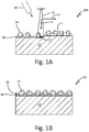
- multi-layer thermal interface material precursor structure 10A may comprise metal substrate 12 and high thermal conductivity electrically insulating particles 14 arranged on a surface S of substrate 12. Particles 14 may be embedded in substrate 12 by locally melting regions on surface S of substrate 12, thereby allowing the particles to be partially immersed in melt pool 17 and to be physically attached to substrate 12 following solidification of melt pool 17 to form layer 18.
- FIG. 1A illustrates how surface S may be locally melted by energy beam 16 focused in the direction of arrow A on surface S. As shown, energy beam 16 may move from left to right in a continuous manner in the direction of arrow B to embed high thermal conductivity particles 14 in surface S to form part of a high thermal conductivity layer.
- Examples of candidate materials for high thermal conductivity particles 14 may include, but are not limited to, in order of decreasing thermal conductivity, diamond, silicon carbide, hexagonal boron nitride, and silicon nitride.
- Examples of candidate materials for metal substrate 12 may include, but are not limited to, nickel, titanium, aluminum, copper, cobalt, tungsten and their alloys and mixtures thereof. In the case where particles 14 are diamond, studies have shown that diamond adhesion in solidified nickel and titanium alloy substrates is high, presumably due to the interfacial formation of a metal carbide during interaction with the molten metal.
- Methods of partially melting surface S may include, but are not limited to, laser melting, RF induction melting, infrared melting electron arc melting, plasma melting, and others known in the art.
- multi-layer precursor thermal interface material 10 may be formed by first assembling an array of particles 14 on surface S of substrate 10 by a computer controlled or manually controlled spreading device. Energy beam 16 may then move over surface S by a computer controlled process to locally melt surface S to allow particles 14 to be partially immersed in melt pool 17, and finally embedded in solidified layer 18 in substrate 12. In other embodiments, particles 14 may be delivered to melt pool 17 by feeder apparatus 19 as energy beam 16 traverses surface S of substrate 12 according to a predetermined pattern in the memory of an additive manufacturing system.
- the areal coverage of the particles in surface S may be from about 20 to 90 percent. More particularly, the areal coverage may be from 30 to 75 percent.
- additive manufacturing processes may include, but are not limited to, laser engineered net shaping (LENS), direct light manufacturing, selective laser melting (SLM), direct laser melting (DLM), laser based additive manufacturing (LBAM), radio frequency induction melting, and others known in the art.
- LENS laser engineered net shaping
- SLM selective laser melting
- DLM direct laser melting
- LBAM laser based additive manufacturing
- radio frequency induction melting and others known in the art.
- Dielectric polymer 20 may be a polymer with electrical resistivity greater than 10 6 ohm-cm.
- Dielectric polymer 20 may be polyimide, polyethylene, nylon, spin on glass, polyester, flyropolymers such asPTFE and others known in the art.
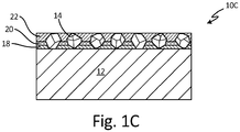
- final thermal insulating material 10C may be formed by depositing metal layer 22 on polymer electrical insulating layer 20 to insure optimum thermal contact between structures mounted on TIM 10C and thermal conducting particles 14.
- Metal layers 22 may be copper, aluminum, gold, silver, nickel, titanium and their alloys and mixtures thereof.
- FIG. 2 is a plot showing the positive effects on thermal conductivity of even a partial coverage of substrate 12 with high thermal conductivity particles 14.
- the thermal conductivity perpendicular to the surface layer as a function of the areal fraction of particles on the surface has been modeled.
- the results are shown in FIG. 2 , where the thermal conductivity of a layer of particles on a surface perpendicular to the surface is plotted against the areal fraction of particles on the surface.
- the lines on the plot are loci of equal values of thermal conductivity (K).
- Alumina has a value of K that is considered to be 20 W/m-°K, while diamond has a value of K that is considered to be 1500 W/m-°K.
- the "star" on the diamond vertical line at a 30% areal fraction of diamond indicates a thermal conductivity of about 400W/m-°K which is 20 times higher than the thermal conductivity of alumina, a common thermal interface material (TIM) in microelectronic packages.
- TIM common thermal interface material
- FIGS. 3A-3D are diagrams illustrating an alternative method to embed high thermal conductivity particles in a metal substrate.
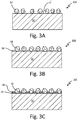
- high thermal conductivity particles 34 are shown distributed on surface S' of metal substrate 32 to form TIM precursor 30A.
- Particles 34 may be distributed on surface S' by means well known in the art and in particular by additive manufacturing technologies.
- An example may be a programmable nozzle to create uniform coverage of particles on surface S'.
- Surface S' of substrate 32 may be melted by using any form of directed energy known in the art.
- surface S' may be subjected to radio frequency (RF) induction that melts surface S' and allows particles 34 to be partially submerged in the melt.
- RF radio frequency
- the particles may be embedded in solidified layer 36 to form precursor thermal interface material 30B as shown in FIG. 3B .
- electrically insulating polymer layer 38 may be deposited on layer 36 to cover the space between particles 34 and to partially cover particles 34 as shown in FIG. 3C .
- thermally insulating material 30D may be formed by depositing metal layer 40 on polymer layer 38 to cover particles 34 to ensure optimum thermal contact between structures mounted on thermal insulating material 30D and thermal conducting particles 14, as shown in FIG. 3D .
- Particles 20 and 34 may have a diameter of from about 1 micron to 100 microns.
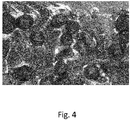
- FIG. 4 shows a scanning electron micrograph of the surface of a nickel substrate containing diamond particles that were spread on the surface by hand and irradiated with an approximately 1KW, 1 micron Nd:YAG laser beam. The particles are clearly embedded in the surface in accord with the claims of the present invention.
- the diamond particles in FIG. 4 are approximately 50 microns in diameter.
- a multi-layer thermal interface structure includes metal substrate and a layer of particles partially covering and partially embedded in a top surface layer of the substrate wherein the particles have a high thermal conductivity and low electrical conductivity.
- a dielectric layer on the top surface layer of the substrate covers the surface between the particles and partially covers the partially embedded particles.
- a metal layer on the dielectric layer covers the partially embedded particles.
- the structure of the preceding paragraph can optionally include, additionally and/or alternatively any, one or more of the following features, configurations and/or additional components:
- the metal may be a nickel alloy.
- the metal substrate may be, or comprise, a nickel alloy.
- the metal may be a titanium alloy.
- the metal substrate may be, or comprise, a titanium alloy.
- the particles may be (e.g. they may be composed of) diamond, boron nitride, silicon nitride, or silicon carbide.
- the dielectric layer may be a polymer, e.g. a polymer with electrical resistivity greater than 10 6 ohm-cm.
- the polymer may be (or is selected from one or more of) a polyimide, polyethylene, nylon, spin on glass, and polyester.
- the particles may have a diameter of from 1 micron to 100 microns.
- the method of the preceding paragraph can optionally include, additional and/or alternatively any, one or more of the following features, configurations, and/or additional components:
- the high thermal conductivity, low electrical conductivity particles may have a diameter from 1 micron to 100 microns.
- the surface coverage of the high thermal conductivity, low electrical conductivity particles on the substrate may be from about 20% to about 90%.
- the surface coverage of the high thermal conductivity, low electrical conductivity particles on the substrate may be from about 30% to about 75%.
- the metal substrate may be, or comprise, titanium, aluminum, copper, cobalt, tungsten, or alloys thereof or mixtures thereof.
- the metal substrate may be, or comprise, nickel, titanium, aluminium, copper, cobalt, tungsten, or alloys thereof, or mixtures thereof.
- the metal may be a nickel alloy.
- the metal substrate may be, or comprise, a nickel alloy.
- Partially melting the top surface of the substrate may include one of more of laser melting, RF induction melting, infrared melting, electric arc melting, and plasma melting.
- the dielectric material may be a polyimide, polyethylene, nylon, spin on glass, and polyester.
- the dielectric material may be a polymer, e.g. a polymer with electrical resistivity greater than 10 6 ohm-cm.
- Partially covering a top surface of the substrate with high thermal conductivity, low electrical conductivity particles and partially melting the top surface of the substrate may comprise and additive manufacturing process.
- the additive manufacturing process may be laser engineered net shaping (LANS or LENS), direct light manufacturing, selective laser melting (SLM), direct laser melting (DLM), laser based additive manufacturing(LBAM), and radio frequency induction melting.
- LENS laser engineered net shaping
- SLM selective laser melting
- DLM direct laser melting
- LBAM laser based additive manufacturing
Landscapes
- Chemical & Material Sciences (AREA)
- Engineering & Computer Science (AREA)
- Ceramic Engineering (AREA)
- Materials Engineering (AREA)
- Cooling Or The Like Of Semiconductors Or Solid State Devices (AREA)
Abstract
Description
- The present invention relates generally to thermal management in electronic packages, and particularly to thermal interface materials.
- Electrical components such as semiconductors, integrated circuit packages, transistors, etc. typically have predesigned temperature limits, below which the electrical components optimally operate. Ideally, the temperatures approximate ambient surroundings. Operations of the components often generate internal heating due to switching losses. If the heat is not removed, the electrical components may then operate at temperatures significantly higher than their normal or desirable operating temperatures. Such excessive temperatures may adversely affect the operating characteristics of the electrical components and the operation of the associated devices. In the extreme case, thermal runaway results, and the device is significantly damaged or even fails completely.
- To avoid or at least reduce the adverse operating characteristics from the heat generation, the heat should be removed, for example by conducting the heat from the operating electrical components to heat sinks. Concurrently, the electrical component often must be electrically isolated from a heat sink and be capable of withstanding breakdown voltages as high as several hundred volts. The heat sinks may then be cooled by conventional convection, radiation or conduction techniques. During conduction, the heat may pass from the operating electrical components to the heat sinks by direct surface contact between the electrical components and heat sinks and/or by contact of the electrical components and heat sink materials through intermediate electrically insulating mediums such as thermal interface materials.
- A multi-layer thermal interface structure includes a substrate with a surface with particles partially covering and partially embedded in the surface wherein the particles have high thermal conductivity and low electrical conductivity. A dielectric layer on the surface fills in the gaps between the partially embedded particles to prevent electrical breakthrough while enabling the effective conduction of heat through the high thermal conductivity particles. A metal layer covers the dielectric layer.
- In an embodiment a method of forming a multi-layer thermal interface structure with a high thermal conductivity and low electrical conductivity top layer on a metallic substrate includes partially covering a top surface of the substrate with electrically insulating particles with high thermal conductivity. Partially melting the top surface of the substrate allows the particles to be partially embedded into the molten surface. Allowing the molten surface to solidify to embed the particles in the surface, covering the space around the partially embedded particles with a dielectric material and covering the dielectric material with a metal layer finishes the process. A further embodiment includes multi-layer thermal interface structures, e.g. multi-layer thermal interface structures as herein described, produced by the methods described herein.
-
-
FIG. 1A is a schematic cross-section showing the formation of the first layer of a multi-layer structure according to an embodiment of the invention. -
FIG. 1B is a schematic cross-section showing the formation of the first two layers according to an embodiment of the invention multi-layer structure ofFIG. 1A . -
FIG. 1C is a schematic cross-section showing the finished multi-layer structure according to an embodiment of the invention. -
FIG. 2 is a plot showing the thermal conductivity of a surface partially covered with particles as a function of the areal density of the coverage. -
FIG. 3A is a schematic cross-section showing a precursor to a multi-layer structure according to an embodiment of the invention. -
FIG. 3B is a schematic cross-section showing the first layer of a multi-layer structure according to an embodiment of the invention. -
FIG. 3C is a schematic cross-section showing the first two layers of a multi-layer structure according to an embodiment of the invention. -
FIG. 3D is a schematic cross-section showing the finished multi-layer structure according to an embodiment of the invention. -
FIG. 4 is a scanning electron micrograph of diamond particles embedded in nickel. - A thermal interface material (TIM) with high dielectric strength suitable for microelectronic applications is disclosed herein.
-
FIGS. 1A and 1B illustrate an embodiment of such a TIM. High thermal conductivity may be realized with a single layer of isolated particles of high thermal conductivity material embedded in a top surface of a current carrying metal substrate. As shown inFIG. 1A , multi-layer thermal interfacematerial precursor structure 10A may comprisemetal substrate 12 and high thermal conductivity electrically insulatingparticles 14 arranged on a surface S ofsubstrate 12.Particles 14 may be embedded insubstrate 12 by locally melting regions on surface S ofsubstrate 12, thereby allowing the particles to be partially immersed inmelt pool 17 and to be physically attached tosubstrate 12 following solidification ofmelt pool 17 to formlayer 18. -
FIG. 1A illustrates how surface S may be locally melted byenergy beam 16 focused in the direction of arrow A on surface S. As shown,energy beam 16 may move from left to right in a continuous manner in the direction of arrow B to embed highthermal conductivity particles 14 in surface S to form part of a high thermal conductivity layer. - Examples of candidate materials for high
thermal conductivity particles 14 may include, but are not limited to, in order of decreasing thermal conductivity, diamond, silicon carbide, hexagonal boron nitride, and silicon nitride. Examples of candidate materials formetal substrate 12 may include, but are not limited to, nickel, titanium, aluminum, copper, cobalt, tungsten and their alloys and mixtures thereof. In the case whereparticles 14 are diamond, studies have shown that diamond adhesion in solidified nickel and titanium alloy substrates is high, presumably due to the interfacial formation of a metal carbide during interaction with the molten metal. - Methods of partially melting surface S may include, but are not limited to, laser melting, RF induction melting, infrared melting electron arc melting, plasma melting, and others known in the art.
- In an additive manufacturing embodiment, multi-layer precursor thermal interface material 10 may be formed by first assembling an array of
particles 14 on surface S of substrate 10 by a computer controlled or manually controlled spreading device.Energy beam 16 may then move over surface S by a computer controlled process to locally melt surface S to allowparticles 14 to be partially immersed inmelt pool 17, and finally embedded in solidifiedlayer 18 insubstrate 12. In other embodiments,particles 14 may be delivered tomelt pool 17 byfeeder apparatus 19 asenergy beam 16 traverses surface S ofsubstrate 12 according to a predetermined pattern in the memory of an additive manufacturing system. - The areal coverage of the particles in surface S may be from about 20 to 90 percent. More particularly, the areal coverage may be from 30 to 75 percent.
- Examples of additive manufacturing processes may include, but are not limited to, laser engineered net shaping (LENS), direct light manufacturing, selective laser melting (SLM), direct laser melting (DLM), laser based additive manufacturing (LBAM), radio frequency induction melting, and others known in the art.
- As shown in
FIG. 1B , to continue forming multi-layer thermal interface material (TIM) structure 10B, the space between partially embeddedparticles 14 may be covered withdielectric polymer 20 to also partially coverparticles 14 to provide electrical insulation betweensubstrate 12 and electrical components mounted on the final structure.Dielectric polymer 20 may be a polymer with electrical resistivity greater than 106 ohm-cm.Dielectric polymer 20 may be polyimide, polyethylene, nylon, spin on glass, polyester, flyropolymers such asPTFE and others known in the art. - As shown in
FIG. 1C , final thermalinsulating material 10C may be formed by depositingmetal layer 22 on polymerelectrical insulating layer 20 to insure optimum thermal contact between structures mounted onTIM 10C andthermal conducting particles 14. Metal layers 22 may be copper, aluminum, gold, silver, nickel, titanium and their alloys and mixtures thereof. - Modeling has indicated the particular significance of even a partial coverage of embedded high
thermal conductivity particles 14 on surface S ofmetal substrate 12.FIG. 2 is a plot showing the positive effects on thermal conductivity of even a partial coverage ofsubstrate 12 with highthermal conductivity particles 14. The thermal conductivity perpendicular to the surface layer as a function of the areal fraction of particles on the surface has been modeled. The results are shown inFIG. 2 , where the thermal conductivity of a layer of particles on a surface perpendicular to the surface is plotted against the areal fraction of particles on the surface. The lines on the plot are loci of equal values of thermal conductivity (K). Alumina has a value of K that is considered to be 20 W/m-°K, while diamond has a value of K that is considered to be 1500 W/m-°K. The "star" on the diamond vertical line at a 30% areal fraction of diamond indicates a thermal conductivity of about 400W/m-°K which is 20 times higher than the thermal conductivity of alumina, a common thermal interface material (TIM) in microelectronic packages. -
FIGS. 3A-3D are diagrams illustrating an alternative method to embed high thermal conductivity particles in a metal substrate. InFIG. 3A , highthermal conductivity particles 34 are shown distributed on surface S' ofmetal substrate 32 to formTIM precursor 30A.Particles 34 may be distributed on surface S' by means well known in the art and in particular by additive manufacturing technologies. An example may be a programmable nozzle to create uniform coverage of particles on surface S'. Surface S' ofsubstrate 32 may be melted by using any form of directed energy known in the art. For example, surface S' may be subjected to radio frequency (RF) induction that melts surface S' and allowsparticles 34 to be partially submerged in the melt. Following solidification, the particles may be embedded in solidifiedlayer 36 to form precursorthermal interface material 30B as shown inFIG. 3B . In the next step, electrically insulatingpolymer layer 38 may be deposited onlayer 36 to cover the space betweenparticles 34 and to partially coverparticles 34 as shown inFIG. 3C . In the final step, thermally insulatingmaterial 30D may be formed by depositingmetal layer 40 onpolymer layer 38 to coverparticles 34 to ensure optimum thermal contact between structures mounted on thermal insulatingmaterial 30D andthermal conducting particles 14, as shown inFIG. 3D . -
Particles - It has been demonstrated that diamond particles can be partially embedded in the surface of metal substrates by irradiating the surface with a laser.
FIG. 4 shows a scanning electron micrograph of the surface of a nickel substrate containing diamond particles that were spread on the surface by hand and irradiated with an approximately 1KW, 1 micron Nd:YAG laser beam. The particles are clearly embedded in the surface in accord with the claims of the present invention. The diamond particles inFIG. 4 are approximately 50 microns in diameter. - The following are non-exclusive descriptions of possible embodiments of the present invention.
- A multi-layer thermal interface structure includes metal substrate and a layer of particles partially covering and partially embedded in a top surface layer of the substrate wherein the particles have a high thermal conductivity and low electrical conductivity. A dielectric layer on the top surface layer of the substrate covers the surface between the particles and partially covers the partially embedded particles. A metal layer on the dielectric layer covers the partially embedded particles.
- The structure of the preceding paragraph can optionally include, additionally and/or alternatively any, one or more of the following features, configurations and/or additional components:
- The metal substrate may be, or comprise, nickel, titanium, aluminum, copper, cobalt, tungsten, or alloys thereof or mixtures thereof.
- The metal may be a nickel alloy. The metal substrate may be, or comprise, a nickel alloy.
- The metal may be a titanium alloy. The metal substrate may be, or comprise, a titanium alloy.
- The particles may be (e.g. they may be composed of) diamond, boron nitride, silicon nitride, or silicon carbide.
- The dielectric layer may be a polymer, e.g. a polymer with electrical resistivity greater than 106 ohm-cm.
- The polymer may be (or is selected from one or more of) a polyimide, polyethylene, nylon, spin on glass, and polyester.
- The particles may have a diameter of from 1 micron to 100 microns.
- A method of forming a multi-layer thermal interface structure, e.g. a multi-layer thermal interface structure as herein described, with high thermal conductivity and low electrical conductivity on a metal substrate may include partially covering a top surface of the substrate with high thermal conductivity, low electrical conductivity particles. Partially melting the top surface of the substrate may cause the particles to sink into the molten layer. Allowing the molten layer to solidify will embed the particles in the substrate. Partially covering the space around the partially embedded particles and partially covering the partially embedded particles with a dielectric material and covering the partially covered particles with a metal layer completes the process.
- The method of the preceding paragraph can optionally include, additional and/or alternatively any, one or more of the following features, configurations, and/or additional components:
- The high thermal conductivity, low electrical conductivity particles may be, e.g. they may be composed of, diamond, boron nitride, silicon nitride or silicon carbide.
- The high thermal conductivity, low electrical conductivity particles may have a diameter from 1 micron to 100 microns.
- The surface coverage of the high thermal conductivity, low electrical conductivity particles on the substrate may be from about 20% to about 90%.
- The surface coverage of the high thermal conductivity, low electrical conductivity particles on the substrate may be from about 30% to about 75%.
- The metal substrate may be, or comprise, titanium, aluminum, copper, cobalt, tungsten, or alloys thereof or mixtures thereof.
- The metal substrate may be, or comprise, nickel, titanium, aluminium, copper, cobalt, tungsten, or alloys thereof, or mixtures thereof.
- The metal may be a nickel alloy. The metal substrate may be, or comprise, a nickel alloy.
- Partially melting the top surface of the substrate may include one of more of laser melting, RF induction melting, infrared melting, electric arc melting, and plasma melting.
- The dielectric material may be a polyimide, polyethylene, nylon, spin on glass, and polyester.
- The dielectric material may be a polymer, e.g. a polymer with electrical resistivity greater than 106 ohm-cm.
- Partially covering a top surface of the substrate with high thermal conductivity, low electrical conductivity particles and partially melting the top surface of the substrate may comprise and additive manufacturing process.
- The additive manufacturing process may be laser engineered net shaping (LANS or LENS), direct light manufacturing, selective laser melting (SLM), direct laser melting (DLM), laser based additive manufacturing(LBAM), and radio frequency induction melting.
- While the invention has been described with reference to an exemplary embodiment(s), it will be understood by those skilled in the art that various changes may be made and equivalents may be substituted for elements thereof without departing from the scope of the invention. In addition, many modifications may be made to adapt a particular situation or material to the teachings of the invention without departing from the essential scope thereof. Therefore, it is intended that the invention not be limited to the particular embodiment(s) disclosed, but that the invention will include all embodiments falling within the scope of the appended claims.
- Certain preferred embodiments of the present invention are as follows:
- 1. A multi-layer thermal interface structure comprising:
- a metal substrate;
- a layer of particles partially covering and partially embedded in a top surface layer of the substrate, wherein the particles have high thermal conductivity and low electrical conductivity;
- a dielectric layer on the top surface layer of the substrate covering the surface between the partially embedded particles and partially covering the particles; and
- a metal layer on the dielectric layer covering the partially embedded particles.
- 2. The structure of embodiment 1, wherein the metal substrate comprises nickel, titanium, aluminum, copper, cobalt, tungsten, or alloys thereof, or mixtures thereof.
- 3. The structure of embodiment 2, wherein the metal substrate is a nickel alloy.
- 4. The structure of embodiment 2, wherein the metal substrate is a titanium alloy.
- 5. The structure of embodiment 1, wherein the particles are composed of diamond, boron nitride, silicon nitride or silicon carbide.
- 6. The structure of embodiment 1, wherein the dielectric layer is a polymer with electrical resistivity greater than 106 ohm-cm.
- 7. The structure of embodiment 6, wherein the polymer is a polyimide, polyethylene, nylon, spin on glass, and polyester.
- 8. The structure of embodiment 5, wherein the particles have a diameter of from 1 micron to 100 microns.
- 9. A method of forming a multi-layer thermal interface structure with a high thermal conductivity and low electrical conductivity on a metal substrate comprising:
- partially covering a top surface of the substrate with high thermal conductivity, low electrical conductivity particles;
- partially melting the top surface of the substrate, thereby causing the particles to sink into the molten layer;
- allowing the molten layer to solidify to embed the particles in the substrate layer;
- partially covering the space around the partially embedded particles and partially covering the partially embedded particles with a dielectric material; and covering the partially covered particles with a metal layer.
- 10. The method of embodiment 9, wherein the high thermal conductivity, low electrical conductivity particles are composed of diamond, boron nitride, silicon nitride or silicon carbide.
- 11. The method of embodiment 9, wherein the high thermal conductivity, low electrical conductivity particles have a diameter of from 1 micron to 100 microns.
- 12. The method of embodiment 9, wherein the surface coverage of the high thermal conductivity, low electrical conductivity particles on the substrate is from about 20% to about 90%.
- 13. The method of
embodiment 12, wherein the surface coverage of the high thermal conductivity, low electrical conductivity particles on the substrate is from about 30% to about 75%. - 14. The method of embodiment 9, wherein the metal substrate comprises nickel, titanium, aluminum, copper, cobalt, tungsten, or alloys thereof, or mixtures thereof.
- 15. The method of
embodiment 14, wherein the metal substrate is a nickel alloy - 16. The method of embodiment 9, wherein partially melting the top surface of the substrate comprises laser melting, RF induction melting, infrared melting, electric arc melting and plasma melting.
- 17. The method of embodiment 9, wherein the dielectric material is a polyimide, polyethylene, nylon, spin on glass, and polyester.
- 18. The method of embodiment 9, wherein the dielectric material is a polymer with electrical resistivity greater than 106 ohm-cm.
- 19. The method of embodiment 9, wherein partially covering a top surface of the substrate with high thermal conductivity, low electrical conductivity particles and partially melting the top surface of the substrate comprises an additive manufacturing process.
- 20. The method of
embodiment 19, wherein the additive manufacturing process comprises laser engineered net shaping (LENS), direct light manufacturing, selective laser melting (SLM), direct laser melting (DLM), laser based additive manufacturing (LBAM), and radio frequency induction melting
Claims (15)
- A multi-layer thermal interface structure comprising:a metal substrate;a layer of particles partially covering and partially embedded in a top surface layer of the substrate, wherein the particles have high thermal conductivity and low electrical conductivity;a dielectric layer on the top surface layer of the substrate covering the surface between the partially embedded particles and partially covering the particles; anda metal layer on the dielectric layer covering the partially embedded particles.
- The structure of claim 1, wherein the metal substrate comprises nickel, titanium, aluminum, copper, cobalt, tungsten, or alloys thereof, or mixtures thereof, preferably wherein the metal substrate is a nickel or titanium alloy.
- The structure of claim 1 or claim 2, wherein the particles are composed of diamond, boron nitride, silicon nitride or silicon carbide, and or wherein the particles have a diameter of from 1 micron to 100 microns.
- The structure of any preceding claim, wherein the dielectric layer is a polymer with electrical resistivity greater than 106 ohm-cm.
- The structure of any preceding claim, wherein the polymer is one or more selected from a polyimide, polyethylene, nylon, spin on glass, and polyester.
- A method of forming a multi-layer thermal interface structure with a high thermal conductivity and low electrical conductivity on a metal substrate comprising:partially covering a top surface of the substrate with high thermal conductivity, low electrical conductivity particles;partially melting the top surface of the substrate, thereby causing the particles to sink into the molten layer;allowing the molten layer to solidify to embed the particles in the substrate layer;partially covering the space around the partially embedded particles and partially covering the partially embedded particles with a dielectric material; andcovering the partially covered particles with a metal layer.
- The method of claim 6, wherein the high thermal conductivity, low electrical conductivity particles are composed of diamond, boron nitride, silicon nitride or silicon carbide, and/or wherein the high thermal conductivity, low electrical conductivity particles have a diameter of from 1 micron to 100 microns.
- The method of claim 6 or claim 7, wherein the surface coverage of the high thermal conductivity, low electrical conductivity particles on the substrate is from about 20% to about 90%, preferably from about 30% to about 75%.
- The method of any one of claims 6 to 8, wherein the metal substrate comprises nickel, titanium, aluminum, copper, cobalt, tungsten, or alloys thereof, or mixtures thereof, preferably wherein the metal substrate is a nickel alloy.
- The method of any one of claims 6 to 9, wherein partially melting the top surface of the substrate comprises one or more of laser melting, RF induction melting, infrared melting, electric arc melting and plasma melting.
- The method of any one of claims 6 to 10, wherein the dielectric material is one or more selected from a polyimide, polyethylene, nylon, spin on glass, and polyester.
- The method of any one of claims 6 to 11, wherein the dielectric material is a polymer with electrical resistivity greater than 106 ohm-cm.
- The method of any one of claims 6 to 12, wherein partially covering a top surface of the substrate with high thermal conductivity, low electrical conductivity particles and partially melting the top surface of the substrate comprises an additive manufacturing process.
- The method of any one of claims 6 to 13, wherein the additive manufacturing process comprises one or more of laser engineered net shaping (LENS), direct light manufacturing, selective laser melting (SLM), direct laser melting (DLM), laser based additive manufacturing (LBAM), and radio frequency induction melting.
- A multi-layer thermal interface structure (e.g. as claimed in any one of claims 1 to 5) produced by the method as claimed in any one of claims 6 to 14.
Applications Claiming Priority (1)
| Application Number | Priority Date | Filing Date | Title |
|---|---|---|---|
| US15/098,597 US10074589B2 (en) | 2016-04-14 | 2016-04-14 | Embedding diamond and other ceramic media into metal substrates to form thermal interface materials |
Publications (2)
| Publication Number | Publication Date |
|---|---|
| EP3232469A1 true EP3232469A1 (en) | 2017-10-18 |
| EP3232469B1 EP3232469B1 (en) | 2021-02-17 |
Family
ID=58387750
Family Applications (1)
| Application Number | Title | Priority Date | Filing Date |
|---|---|---|---|
| EP17161859.8A Active EP3232469B1 (en) | 2016-04-14 | 2017-03-20 | Embedding diamond and other ceramic media into metal substrates to form thermal interface materials |
Country Status (2)
| Country | Link |
|---|---|
| US (1) | US10074589B2 (en) |
| EP (1) | EP3232469B1 (en) |
Cited By (1)
| Publication number | Priority date | Publication date | Assignee | Title |
|---|---|---|---|---|
| CN115706038A (en) * | 2021-08-03 | 2023-02-17 | 中微半导体设备(上海)股份有限公司 | Electrostatic chuck, manufacturing method, refurbishing method and plasma reaction device |
Families Citing this family (2)
| Publication number | Priority date | Publication date | Assignee | Title |
|---|---|---|---|---|
| US10937716B2 (en) * | 2017-12-12 | 2021-03-02 | Arizona Board Of Regents On Behalf Of Arizona State University | Multi-layer thin film composite thermal interface materials |
| US12187951B2 (en) * | 2020-07-27 | 2025-01-07 | Google Llc | Thermal interface material and method for making the same |
Citations (8)
| Publication number | Priority date | Publication date | Assignee | Title |
|---|---|---|---|---|
| US4782893A (en) * | 1986-09-15 | 1988-11-08 | Trique Concepts, Inc. | Electrically insulating thermally conductive pad for mounting electronic components |
| JP2006270062A (en) * | 2005-02-22 | 2006-10-05 | Mitsubishi Materials Corp | Insulated heat transfer structure and power module substrate |
| JP2007214492A (en) * | 2006-02-13 | 2007-08-23 | Mitsubishi Materials Corp | Insulated heat transfer structure, power module substrate, and method of manufacturing insulated heat transfer structure |
| US20100319897A1 (en) * | 2009-06-19 | 2010-12-23 | Shih-Yao Huang | High-performance heat dissipation substrate with monoparticle layer |
| US20110024101A1 (en) * | 2009-07-31 | 2011-02-03 | Korea Electronics Technology Institute | Thermal conductive substrate and method of manufacturing the same |
| US20110044004A1 (en) * | 2009-08-18 | 2011-02-24 | Garosshen Thomas J | Heat transfer apparatus having a thermal interface material |
| JP2012227271A (en) * | 2011-04-18 | 2012-11-15 | Cmk Corp | Insulating/heat dissipating substrate for power module |
| JP2013131662A (en) * | 2011-12-22 | 2013-07-04 | Cmk Corp | Insulating/heat dissipating substrate for power module and method for manufacturing the same |
Family Cites Families (8)
| Publication number | Priority date | Publication date | Assignee | Title |
|---|---|---|---|---|
| US6808817B2 (en) * | 2002-03-15 | 2004-10-26 | Delphi Technologies, Inc. | Kinetically sprayed aluminum metal matrix composites for thermal management |
| AT7382U1 (en) | 2003-03-11 | 2005-02-25 | Plansee Ag | HEAT SINK WITH HIGH HEAT-CONDUCTIVITY |
| US7164197B2 (en) * | 2003-06-19 | 2007-01-16 | 3M Innovative Properties Company | Dielectric composite material |
| US7279023B2 (en) | 2003-10-02 | 2007-10-09 | Materials And Electrochemical Research (Mer) Corporation | High thermal conductivity metal matrix composites |
| DE102010055201A1 (en) | 2010-12-20 | 2012-06-21 | Eads Deutschland Gmbh | Method for producing a component |
| WO2013142580A1 (en) * | 2012-03-20 | 2013-09-26 | Applied Nanotech Holdings, Inc. | Application of dielectric layer and circuit traces on heat sink |
| US9515004B2 (en) | 2013-03-15 | 2016-12-06 | Laird Technologies, Inc. | Thermal interface materials |
| US9024436B2 (en) * | 2013-06-19 | 2015-05-05 | Broadcom Corporation | Thermal interface material for integrated circuit package |
-
2016
- 2016-04-14 US US15/098,597 patent/US10074589B2/en active Active
-
2017
- 2017-03-20 EP EP17161859.8A patent/EP3232469B1/en active Active
Patent Citations (8)
| Publication number | Priority date | Publication date | Assignee | Title |
|---|---|---|---|---|
| US4782893A (en) * | 1986-09-15 | 1988-11-08 | Trique Concepts, Inc. | Electrically insulating thermally conductive pad for mounting electronic components |
| JP2006270062A (en) * | 2005-02-22 | 2006-10-05 | Mitsubishi Materials Corp | Insulated heat transfer structure and power module substrate |
| JP2007214492A (en) * | 2006-02-13 | 2007-08-23 | Mitsubishi Materials Corp | Insulated heat transfer structure, power module substrate, and method of manufacturing insulated heat transfer structure |
| US20100319897A1 (en) * | 2009-06-19 | 2010-12-23 | Shih-Yao Huang | High-performance heat dissipation substrate with monoparticle layer |
| US20110024101A1 (en) * | 2009-07-31 | 2011-02-03 | Korea Electronics Technology Institute | Thermal conductive substrate and method of manufacturing the same |
| US20110044004A1 (en) * | 2009-08-18 | 2011-02-24 | Garosshen Thomas J | Heat transfer apparatus having a thermal interface material |
| JP2012227271A (en) * | 2011-04-18 | 2012-11-15 | Cmk Corp | Insulating/heat dissipating substrate for power module |
| JP2013131662A (en) * | 2011-12-22 | 2013-07-04 | Cmk Corp | Insulating/heat dissipating substrate for power module and method for manufacturing the same |
Cited By (1)
| Publication number | Priority date | Publication date | Assignee | Title |
|---|---|---|---|---|
| CN115706038A (en) * | 2021-08-03 | 2023-02-17 | 中微半导体设备(上海)股份有限公司 | Electrostatic chuck, manufacturing method, refurbishing method and plasma reaction device |
Also Published As
| Publication number | Publication date |
|---|---|
| US20170301605A1 (en) | 2017-10-19 |
| EP3232469B1 (en) | 2021-02-17 |
| US10074589B2 (en) | 2018-09-11 |
Similar Documents
| Publication | Publication Date | Title |
|---|---|---|
| US11594475B2 (en) | Method of fabricating an electronic power module by additive manufacturing, and associated substrate and module | |
| TWI492303B (en) | Buffer layer for enhanced light and/or laser sintering | |
| US9412658B2 (en) | Constrained nanosecond laser anneal of metal interconnect structures | |
| EP3232469B1 (en) | Embedding diamond and other ceramic media into metal substrates to form thermal interface materials | |
| US9111924B2 (en) | Flip-chip hybridization of microelectronic components by local heating of connecting elements | |
| US9190375B2 (en) | Solder bump reflow by induction heating | |
| CN1757112A (en) | Micro fuse | |
| CN101237746A (en) | Electronic board with heating resistors | |
| US11147851B2 (en) | Method of fabricating an electronic power module by additive manufacturing, and associated substrate and module | |
| US12604752B2 (en) | Semiconductor die package | |
| CN109075125B (en) | Method for filling a via hole of a ceramic substrate and ceramic substrate via hole filler formed thereby | |
| US20150004400A1 (en) | Support assembly for use in semiconductor manufacturing tools with a fusible bond | |
| US20180277491A1 (en) | Power electronics assemblies and vehicles incorporating the same | |
| CN103428992A (en) | Circuit board, electronic module, lighting device and method for manufacturing circuit board | |
| US5940727A (en) | Technique for producing interconnecting conductive links | |
| JP4492257B2 (en) | Semiconductor module and manufacturing method thereof | |
| TWI677958B (en) | Power semiconductor module device and method for manufacturing power semiconductor module | |
| JP5644806B2 (en) | Insulating substrate, semiconductor device and manufacturing method thereof | |
| US9165915B2 (en) | Flip-chip hybridization of microelectronic components using suspended fusible resistive connection elements | |
| JP2016502758A (en) | Graphene interposer and method for producing the interposer | |
| CN102267260A (en) | Substrate having laser sintered underplate | |
| JP2001144035A (en) | Semiconductor device manufacturing method and semiconductor device | |
| JP2847549B2 (en) | Method for manufacturing semiconductor device | |
| JP5287556B2 (en) | LCP multilayer substrate and manufacturing method thereof | |
| JPS63137455A (en) | Manufacture of semiconductor device |
Legal Events
| Date | Code | Title | Description |
|---|---|---|---|
| PUAI | Public reference made under article 153(3) epc to a published international application that has entered the european phase |
Free format text: ORIGINAL CODE: 0009012 |
|
| STAA | Information on the status of an ep patent application or granted ep patent |
Free format text: STATUS: THE APPLICATION HAS BEEN PUBLISHED |
|
| AK | Designated contracting states |
Kind code of ref document: A1 Designated state(s): AL AT BE BG CH CY CZ DE DK EE ES FI FR GB GR HR HU IE IS IT LI LT LU LV MC MK MT NL NO PL PT RO RS SE SI SK SM TR |
|
| AX | Request for extension of the european patent |
Extension state: BA ME |
|
| STAA | Information on the status of an ep patent application or granted ep patent |
Free format text: STATUS: REQUEST FOR EXAMINATION WAS MADE |
|
| 17P | Request for examination filed |
Effective date: 20180403 |
|
| RBV | Designated contracting states (corrected) |
Designated state(s): AL AT BE BG CH CY CZ DE DK EE ES FI FR GB GR HR HU IE IS IT LI LT LU LV MC MK MT NL NO PL PT RO RS SE SI SK SM TR |
|
| GRAP | Despatch of communication of intention to grant a patent |
Free format text: ORIGINAL CODE: EPIDOSNIGR1 |
|
| STAA | Information on the status of an ep patent application or granted ep patent |
Free format text: STATUS: GRANT OF PATENT IS INTENDED |
|
| INTG | Intention to grant announced |
Effective date: 20200902 |
|
| GRAS | Grant fee paid |
Free format text: ORIGINAL CODE: EPIDOSNIGR3 |
|
| GRAA | (expected) grant |
Free format text: ORIGINAL CODE: 0009210 |
|
| STAA | Information on the status of an ep patent application or granted ep patent |
Free format text: STATUS: THE PATENT HAS BEEN GRANTED |
|
| AK | Designated contracting states |
Kind code of ref document: B1 Designated state(s): AL AT BE BG CH CY CZ DE DK EE ES FI FR GB GR HR HU IE IS IT LI LT LU LV MC MK MT NL NO PL PT RO RS SE SI SK SM TR |
|
| REG | Reference to a national code |
Ref country code: GB Ref legal event code: FG4D |
|
| REG | Reference to a national code |
Ref country code: CH Ref legal event code: EP |
|
| REG | Reference to a national code |
Ref country code: DE Ref legal event code: R096 Ref document number: 602017032481 Country of ref document: DE |
|
| REG | Reference to a national code |
Ref country code: AT Ref legal event code: REF Ref document number: 1362590 Country of ref document: AT Kind code of ref document: T Effective date: 20210315 |
|
| REG | Reference to a national code |
Ref country code: IE Ref legal event code: FG4D |
|
| REG | Reference to a national code |
Ref country code: LT Ref legal event code: MG9D |
|
| REG | Reference to a national code |
Ref country code: NL Ref legal event code: MP Effective date: 20210217 |
|
| PG25 | Lapsed in a contracting state [announced via postgrant information from national office to epo] |
Ref country code: BG Free format text: LAPSE BECAUSE OF FAILURE TO SUBMIT A TRANSLATION OF THE DESCRIPTION OR TO PAY THE FEE WITHIN THE PRESCRIBED TIME-LIMIT Effective date: 20210517 Ref country code: LT Free format text: LAPSE BECAUSE OF FAILURE TO SUBMIT A TRANSLATION OF THE DESCRIPTION OR TO PAY THE FEE WITHIN THE PRESCRIBED TIME-LIMIT Effective date: 20210217 Ref country code: HR Free format text: LAPSE BECAUSE OF FAILURE TO SUBMIT A TRANSLATION OF THE DESCRIPTION OR TO PAY THE FEE WITHIN THE PRESCRIBED TIME-LIMIT Effective date: 20210217 Ref country code: GR Free format text: LAPSE BECAUSE OF FAILURE TO SUBMIT A TRANSLATION OF THE DESCRIPTION OR TO PAY THE FEE WITHIN THE PRESCRIBED TIME-LIMIT Effective date: 20210518 Ref country code: FI Free format text: LAPSE BECAUSE OF FAILURE TO SUBMIT A TRANSLATION OF THE DESCRIPTION OR TO PAY THE FEE WITHIN THE PRESCRIBED TIME-LIMIT Effective date: 20210217 Ref country code: NO Free format text: LAPSE BECAUSE OF FAILURE TO SUBMIT A TRANSLATION OF THE DESCRIPTION OR TO PAY THE FEE WITHIN THE PRESCRIBED TIME-LIMIT Effective date: 20210517 Ref country code: PT Free format text: LAPSE BECAUSE OF FAILURE TO SUBMIT A TRANSLATION OF THE DESCRIPTION OR TO PAY THE FEE WITHIN THE PRESCRIBED TIME-LIMIT Effective date: 20210617 |
|
| REG | Reference to a national code |
Ref country code: AT Ref legal event code: MK05 Ref document number: 1362590 Country of ref document: AT Kind code of ref document: T Effective date: 20210217 |
|
| PG25 | Lapsed in a contracting state [announced via postgrant information from national office to epo] |
Ref country code: SE Free format text: LAPSE BECAUSE OF FAILURE TO SUBMIT A TRANSLATION OF THE DESCRIPTION OR TO PAY THE FEE WITHIN THE PRESCRIBED TIME-LIMIT Effective date: 20210217 Ref country code: RS Free format text: LAPSE BECAUSE OF FAILURE TO SUBMIT A TRANSLATION OF THE DESCRIPTION OR TO PAY THE FEE WITHIN THE PRESCRIBED TIME-LIMIT Effective date: 20210217 Ref country code: LV Free format text: LAPSE BECAUSE OF FAILURE TO SUBMIT A TRANSLATION OF THE DESCRIPTION OR TO PAY THE FEE WITHIN THE PRESCRIBED TIME-LIMIT Effective date: 20210217 Ref country code: NL Free format text: LAPSE BECAUSE OF FAILURE TO SUBMIT A TRANSLATION OF THE DESCRIPTION OR TO PAY THE FEE WITHIN THE PRESCRIBED TIME-LIMIT Effective date: 20210217 Ref country code: PL Free format text: LAPSE BECAUSE OF FAILURE TO SUBMIT A TRANSLATION OF THE DESCRIPTION OR TO PAY THE FEE WITHIN THE PRESCRIBED TIME-LIMIT Effective date: 20210217 |
|
| PG25 | Lapsed in a contracting state [announced via postgrant information from national office to epo] |
Ref country code: IS Free format text: LAPSE BECAUSE OF FAILURE TO SUBMIT A TRANSLATION OF THE DESCRIPTION OR TO PAY THE FEE WITHIN THE PRESCRIBED TIME-LIMIT Effective date: 20210617 |
|
| PG25 | Lapsed in a contracting state [announced via postgrant information from national office to epo] |
Ref country code: SM Free format text: LAPSE BECAUSE OF FAILURE TO SUBMIT A TRANSLATION OF THE DESCRIPTION OR TO PAY THE FEE WITHIN THE PRESCRIBED TIME-LIMIT Effective date: 20210217 Ref country code: AT Free format text: LAPSE BECAUSE OF FAILURE TO SUBMIT A TRANSLATION OF THE DESCRIPTION OR TO PAY THE FEE WITHIN THE PRESCRIBED TIME-LIMIT Effective date: 20210217 Ref country code: CZ Free format text: LAPSE BECAUSE OF FAILURE TO SUBMIT A TRANSLATION OF THE DESCRIPTION OR TO PAY THE FEE WITHIN THE PRESCRIBED TIME-LIMIT Effective date: 20210217 Ref country code: EE Free format text: LAPSE BECAUSE OF FAILURE TO SUBMIT A TRANSLATION OF THE DESCRIPTION OR TO PAY THE FEE WITHIN THE PRESCRIBED TIME-LIMIT Effective date: 20210217 |
|
| REG | Reference to a national code |
Ref country code: CH Ref legal event code: PL |
|
| REG | Reference to a national code |
Ref country code: DE Ref legal event code: R097 Ref document number: 602017032481 Country of ref document: DE |
|
| PG25 | Lapsed in a contracting state [announced via postgrant information from national office to epo] |
Ref country code: RO Free format text: LAPSE BECAUSE OF FAILURE TO SUBMIT A TRANSLATION OF THE DESCRIPTION OR TO PAY THE FEE WITHIN THE PRESCRIBED TIME-LIMIT Effective date: 20210217 Ref country code: SK Free format text: LAPSE BECAUSE OF FAILURE TO SUBMIT A TRANSLATION OF THE DESCRIPTION OR TO PAY THE FEE WITHIN THE PRESCRIBED TIME-LIMIT Effective date: 20210217 Ref country code: MC Free format text: LAPSE BECAUSE OF FAILURE TO SUBMIT A TRANSLATION OF THE DESCRIPTION OR TO PAY THE FEE WITHIN THE PRESCRIBED TIME-LIMIT Effective date: 20210217 Ref country code: DK Free format text: LAPSE BECAUSE OF FAILURE TO SUBMIT A TRANSLATION OF THE DESCRIPTION OR TO PAY THE FEE WITHIN THE PRESCRIBED TIME-LIMIT Effective date: 20210217 |
|
| REG | Reference to a national code |
Ref country code: BE Ref legal event code: MM Effective date: 20210331 |
|
| PLBE | No opposition filed within time limit |
Free format text: ORIGINAL CODE: 0009261 |
|
| STAA | Information on the status of an ep patent application or granted ep patent |
Free format text: STATUS: NO OPPOSITION FILED WITHIN TIME LIMIT |
|
| 26N | No opposition filed |
Effective date: 20211118 |
|
| PG25 | Lapsed in a contracting state [announced via postgrant information from national office to epo] |
Ref country code: IE Free format text: LAPSE BECAUSE OF NON-PAYMENT OF DUE FEES Effective date: 20210320 Ref country code: ES Free format text: LAPSE BECAUSE OF FAILURE TO SUBMIT A TRANSLATION OF THE DESCRIPTION OR TO PAY THE FEE WITHIN THE PRESCRIBED TIME-LIMIT Effective date: 20210217 Ref country code: AL Free format text: LAPSE BECAUSE OF FAILURE TO SUBMIT A TRANSLATION OF THE DESCRIPTION OR TO PAY THE FEE WITHIN THE PRESCRIBED TIME-LIMIT Effective date: 20210217 Ref country code: CH Free format text: LAPSE BECAUSE OF NON-PAYMENT OF DUE FEES Effective date: 20210331 Ref country code: LU Free format text: LAPSE BECAUSE OF NON-PAYMENT OF DUE FEES Effective date: 20210320 Ref country code: LI Free format text: LAPSE BECAUSE OF NON-PAYMENT OF DUE FEES Effective date: 20210331 |
|
| PG25 | Lapsed in a contracting state [announced via postgrant information from national office to epo] |
Ref country code: SI Free format text: LAPSE BECAUSE OF FAILURE TO SUBMIT A TRANSLATION OF THE DESCRIPTION OR TO PAY THE FEE WITHIN THE PRESCRIBED TIME-LIMIT Effective date: 20210217 |
|
| PG25 | Lapsed in a contracting state [announced via postgrant information from national office to epo] |
Ref country code: IT Free format text: LAPSE BECAUSE OF FAILURE TO SUBMIT A TRANSLATION OF THE DESCRIPTION OR TO PAY THE FEE WITHIN THE PRESCRIBED TIME-LIMIT Effective date: 20210217 |
|
| PG25 | Lapsed in a contracting state [announced via postgrant information from national office to epo] |
Ref country code: IS Free format text: LAPSE BECAUSE OF FAILURE TO SUBMIT A TRANSLATION OF THE DESCRIPTION OR TO PAY THE FEE WITHIN THE PRESCRIBED TIME-LIMIT Effective date: 20210617 |
|
| PG25 | Lapsed in a contracting state [announced via postgrant information from national office to epo] |
Ref country code: BE Free format text: LAPSE BECAUSE OF NON-PAYMENT OF DUE FEES Effective date: 20210331 |
|
| PG25 | Lapsed in a contracting state [announced via postgrant information from national office to epo] |
Ref country code: HU Free format text: LAPSE BECAUSE OF FAILURE TO SUBMIT A TRANSLATION OF THE DESCRIPTION OR TO PAY THE FEE WITHIN THE PRESCRIBED TIME-LIMIT; INVALID AB INITIO Effective date: 20170320 |
|
| P01 | Opt-out of the competence of the unified patent court (upc) registered |
Effective date: 20230522 |
|
| PG25 | Lapsed in a contracting state [announced via postgrant information from national office to epo] |
Ref country code: CY Free format text: LAPSE BECAUSE OF FAILURE TO SUBMIT A TRANSLATION OF THE DESCRIPTION OR TO PAY THE FEE WITHIN THE PRESCRIBED TIME-LIMIT Effective date: 20210217 |
|
| PG25 | Lapsed in a contracting state [announced via postgrant information from national office to epo] |
Ref country code: MK Free format text: LAPSE BECAUSE OF FAILURE TO SUBMIT A TRANSLATION OF THE DESCRIPTION OR TO PAY THE FEE WITHIN THE PRESCRIBED TIME-LIMIT Effective date: 20210217 |
|
| PG25 | Lapsed in a contracting state [announced via postgrant information from national office to epo] |
Ref country code: MT Free format text: LAPSE BECAUSE OF FAILURE TO SUBMIT A TRANSLATION OF THE DESCRIPTION OR TO PAY THE FEE WITHIN THE PRESCRIBED TIME-LIMIT Effective date: 20210217 |
|
| REG | Reference to a national code |
Ref country code: DE Ref legal event code: R079 Ref document number: 602017032481 Country of ref document: DE Free format text: PREVIOUS MAIN CLASS: H01L0023373000 Ipc: H10W0040250000 |
|
| PG25 | Lapsed in a contracting state [announced via postgrant information from national office to epo] |
Ref country code: TR Free format text: LAPSE BECAUSE OF FAILURE TO SUBMIT A TRANSLATION OF THE DESCRIPTION OR TO PAY THE FEE WITHIN THE PRESCRIBED TIME-LIMIT Effective date: 20210217 |
|
| PGFP | Annual fee paid to national office [announced via postgrant information from national office to epo] |
Ref country code: GB Payment date: 20260219 Year of fee payment: 10 |
|
| PGFP | Annual fee paid to national office [announced via postgrant information from national office to epo] |
Ref country code: DE Payment date: 20260219 Year of fee payment: 10 |
|
| PGFP | Annual fee paid to national office [announced via postgrant information from national office to epo] |
Ref country code: FR Payment date: 20260219 Year of fee payment: 10 |