EP3229270A1 - Integrated circuit power distribution network - Google Patents
Integrated circuit power distribution network Download PDFInfo
- Publication number
- EP3229270A1 EP3229270A1 EP16164134.5A EP16164134A EP3229270A1 EP 3229270 A1 EP3229270 A1 EP 3229270A1 EP 16164134 A EP16164134 A EP 16164134A EP 3229270 A1 EP3229270 A1 EP 3229270A1
- Authority
- EP
- European Patent Office
- Prior art keywords
- metal layer
- power
- stack
- integrated circuit
- distribution network
- Prior art date
- Legal status (The legal status is an assumption and is not a legal conclusion. Google has not performed a legal analysis and makes no representation as to the accuracy of the status listed.)
- Pending
Links
Images



Classifications
-
- H—ELECTRICITY
- H10—SEMICONDUCTOR DEVICES; ELECTRIC SOLID-STATE DEVICES NOT OTHERWISE PROVIDED FOR
- H10D—INORGANIC ELECTRIC SEMICONDUCTOR DEVICES
- H10D84/00—Integrated devices formed in or on semiconductor substrates that comprise only semiconducting layers, e.g. on Si wafers or on GaAs-on-Si wafers
- H10D84/90—Masterslice integrated circuits
- H10D84/903—Masterslice integrated circuits comprising field effect technology
- H10D84/907—CMOS gate arrays
-
- H—ELECTRICITY
- H10—SEMICONDUCTOR DEVICES; ELECTRIC SOLID-STATE DEVICES NOT OTHERWISE PROVIDED FOR
- H10D—INORGANIC ELECTRIC SEMICONDUCTOR DEVICES
- H10D89/00—Aspects of integrated devices not covered by groups H10D84/00 - H10D88/00
- H10D89/10—Integrated device layouts
-
- H—ELECTRICITY
- H10—SEMICONDUCTOR DEVICES; ELECTRIC SOLID-STATE DEVICES NOT OTHERWISE PROVIDED FOR
- H10W—GENERIC PACKAGES, INTERCONNECTIONS, CONNECTORS OR OTHER CONSTRUCTIONAL DETAILS OF DEVICES COVERED BY CLASS H10
- H10W20/00—Interconnections in chips, wafers or substrates
- H10W20/40—Interconnections external to wafers or substrates, e.g. back-end-of-line [BEOL] metallisations or vias connecting to gate electrodes
- H10W20/41—Interconnections external to wafers or substrates, e.g. back-end-of-line [BEOL] metallisations or vias connecting to gate electrodes characterised by their conductive parts
- H10W20/427—Power or ground buses
-
- H—ELECTRICITY
- H10—SEMICONDUCTOR DEVICES; ELECTRIC SOLID-STATE DEVICES NOT OTHERWISE PROVIDED FOR
- H10D—INORGANIC ELECTRIC SEMICONDUCTOR DEVICES
- H10D84/00—Integrated devices formed in or on semiconductor substrates that comprise only semiconducting layers, e.g. on Si wafers or on GaAs-on-Si wafers
- H10D84/90—Masterslice integrated circuits
- H10D84/903—Masterslice integrated circuits comprising field effect technology
- H10D84/907—CMOS gate arrays
- H10D84/968—Macro-architecture
- H10D84/974—Layout specifications, i.e. inner core regions
- H10D84/975—Wiring regions or routing
-
- H—ELECTRICITY
- H10—SEMICONDUCTOR DEVICES; ELECTRIC SOLID-STATE DEVICES NOT OTHERWISE PROVIDED FOR
- H10D—INORGANIC ELECTRIC SEMICONDUCTOR DEVICES
- H10D84/00—Integrated devices formed in or on semiconductor substrates that comprise only semiconducting layers, e.g. on Si wafers or on GaAs-on-Si wafers
- H10D84/90—Masterslice integrated circuits
- H10D84/903—Masterslice integrated circuits comprising field effect technology
- H10D84/907—CMOS gate arrays
- H10D84/968—Macro-architecture
- H10D84/974—Layout specifications, i.e. inner core regions
- H10D84/981—Power supply lines
-
- H—ELECTRICITY
- H10—SEMICONDUCTOR DEVICES; ELECTRIC SOLID-STATE DEVICES NOT OTHERWISE PROVIDED FOR
- H10D—INORGANIC ELECTRIC SEMICONDUCTOR DEVICES
- H10D84/00—Integrated devices formed in or on semiconductor substrates that comprise only semiconducting layers, e.g. on Si wafers or on GaAs-on-Si wafers
- H10D84/90—Masterslice integrated circuits
- H10D84/903—Masterslice integrated circuits comprising field effect technology
- H10D84/907—CMOS gate arrays
- H10D84/983—Levels of metallisation
- H10D84/988—Four or more levels of metal
Definitions
- the invention relates to the field of integrated solid state semiconductor devices using standard-cell design methodologies. More specifically it relates to an integrated circuit device comprising a power distribution network and a related method of manufacture.
- Standard-cell design in current high-performance CMOS platform technology involves tight contacted poly pitch constraints and metallization pitch constraints.
- Standard-cell architectures are known in the art for predetermined cell track heights, e.g. 9-track, 7.5-track or 6-track standard-cell libraries may be available, for example, for 32 nm metallization pitch technology.
- self-aligned double patterning and self-aligned quadruple patterning techniques used for state-of-the-art device manufacture impose strict design constraints.
- a plurality of standard cells are arranged in at least one row in a front-of-the-line portion of the device, e.g. a bottom portion of the device manufactured directly in and on the semiconductor substrate.
- Current standard cell technology may also involve a middle-of-line portion for enabling an efficient internal layout of the standard cells.
- This middle-of-line portion may comprise a metal layer for internal routing of signals and/or power supply in the standard cell.
- This middle-of-line portion may advantageously comprise, as known in the art, a power rail to provide efficient source and/or drain power tapping at the lowest level in the power distribution architecture.
- current 7.5-track cells may be designed with such inbound Vss/Vdd power rail in a metal layer of the middle-of-line portion.
- a power distribution network is typically provided in integrated circuit devices to supply a ground and power supply voltage pair to the solid state devices integrated in and/or on the semiconductor substrate, e.g. to transistors provided in the front-of-the-line portion of the device.
- This power distribution network may receive such voltage pair from external connections, e.g. provided at a top level of the semiconductor stack, and route these voltages via metal tracks provided in metal layers, e.g. interconnected by vias, to a level where the semiconductor transistors of the integrated device are arranged, e.g. a lowest level of the network near the semiconductor substrate at the bottom of the stack.
- wide power rails 21 may be provided in a metal layer M2. These power rails may run perpendicular to the gate orientation y of the standard cells 23.
- the metal layer M2 being the first metal layer having tracks in this direction x above the intra-cell integration level, e.g. above the front-end-of-the-line (FEOL) and middle-of-line (MOL) levels, e.g. above a middle-of-line internal routing layer M0 that provides an interface between the low-level cell components and the cell integration wiring of the back-of-the-line (BEOL), could provide valuable routing resources which are consumed by such power rail structures 21.
- FEOL front-end-of-the-line
- MOL middle-of-line internal routing layer M0 that provides an interface between the low-level cell components and the cell integration wiring of the back-of-the-line (BEOL)
- These wide power rails 21 may be, for example, provided at a periodicity along the direction y corresponding to the cell height, e.g. at cell height frequency.
- the width of these power rails may be constrained by design requirements, e.g. to 3 critical dimensions (CD), as required by self-aligned quadruple patterning technology.
- internal power rails 22, as part of the standard cell 23, may thus run along the direction x in the internal routing layer M0 .
- These internal power rails may be connected to abutting or otherwise adjacent cells in the row direction x.
- This internal power rails may be connected, e.g. by vias, to short, interconnecting metal traces 24 orientated along the direction x in a metal layer M1, which provide the connection, e.g. by vias, to the power rails 21 in metal layer M2.
- power is transferred, as indicated by the bold arrows 25 in FIG 3 from metal layer M2, via the stitching straps 24 in metal layer M1 , to the internal power rail 22 in the internal routing layer M0.
- a disadvantage of this approach is that, for a 7.5-track cell, only 5 of the 7.5 tracks on metal layer M2 may be available for signal routing, while the rest is consumed by power routing.
- current 7.5 track-height cells may be designed with such internal inbound Vdd and Vss power rails 22 to provide easy power tapping to the source and drain regions of the transistors integrated in the standard cell. Furthermore, it is also known in the art to design 6 track-height cells having an outbound buried power rail to free up some of the resources used in the M2 layer for signal routing.
- routing resources in the lowest metal routing layers in a semiconductor stack are available for signal routing in a direction perpendicular to the gate orientation and parallel to the substrate.
- embodiments of the present invention relate to an integrated circuit device comprising a stack of layers and a semiconductor substrate forming a bottom level of this stack, e.g. an IC device comprising a stack consisting of a semiconductor substrate and a plurality of layers stacked thereon, e.g. an IC device comprising a stack of layers on a semiconductor substrate.
- the integrated circuit device comprises a plurality of standard cells, each standard cell comprising a plurality of integrated transistors and interconnecting structures for locally interconnecting the transistors such as to provide a predetermined function of the standard cell.
- the standard cells comprise parallel gate structures oriented in a first direction that is parallel to the substrate.
- the standard cell e.g.
- each standard cell comprises at least one internal power pin, e.g. a power connector that is internal in the cell, for supplying a reference voltage to contacts of the integrated transistors in accordance with the predetermined function of the standard cell.
- the stack of layers further comprises a plurality of metal layers in which conductive metal lines are formed to route signals between the standard cells.
- the metal lines in each metal layer have a preferred orientation, in which each metal layer has a preferred orientation that is orthogonal to the preferred orientation of the metal lines in an adjacent metal layer of the plurality of metal layers.
- a first metal layer, e.g. a vertical metal layer, e.g. a first vertical metal layer, of the plurality of metal layers is the lowest metal layer in the stack, e.g. of the stack, that has the first direction as preferred orientation and that provides routing resources for signal routing between the standard cells.
- a second metal layer, e.g. a horizontal metal layer, e.g. a second horizontal metal layer, of the plurality of metal layers is the nearest metal layer above the first vertical metal layer in the stack.
- the integrated circuit device further comprises a power distribution network for delivering the reference voltage to the at least one internal power pin.
- a power distribution network for delivering the reference voltage to the at least one internal power pin.
- the at least one internal power pin may comprise a buried power rail.
- the at least one internal power pin may comprise an internal power rail extending in the second direction, in which this internal power rail may be provided in a local interconnect metal layer of the standard cells.
- the stack may comprise at least one layer fabricated using multiple patterning, e.g. LELE, LELELE or such.
- the at least one layer may be fabricated using self-aligned double patterning or self-aligned quadruple patterning.
- the power distribution network may comprise at least one power rail oriented along the first direction and provided in the first vertical metal layer.
- the power distribution network may comprise at least one power rail oriented along said first direction and provided in a third vertical metal layer of the plurality of metal layers, in which this third vertical metal layer refers to the nearest metal layer above the second horizontal metal layer in the stack.
- the power distribution network may comprise at least one power staple in the second horizontal metal layer for electrically connecting the power rail in the third vertical metal layer to the power rail in the first vertical metal layer.
- the second horizontal metal layer may have a larger pitch than the smallest pitch of the other metal layers in the stack.
- the second horizontal metal layer may have a larger pitch than the smallest pitch of the other horizontal metal layers in the stack.
- the power distribution network may comprise at least one power strap oriented along the second direction.
- This at least one power strap may be provided in a horizontal metal layer above the first vertical metal layer, e.g. in the second horizontal metal layer.
- This at least one power strap may be adapted for locally connecting, e.g. electrically interconnecting, two power rails that are oriented along the first direction and provided in the first vertical metal layer.
- The, or each, at least one power strap may for example electrically connect at most four power rails oriented along the first direction and provided in the first vertical metal layer.
- The, or each, at least one power strap may for example electrically connect at most two power rails oriented along the first direction and provided in the first vertical metal layer.
- the at least one power strap may form part of a conductive path electrically connecting a further metal layer above the second horizontal metal layer to the at least one internal power pin.
- the at least one power strap may form part of a conductive path electrically connecting a further metal layer above the second horizontal metal layer to a further internal power pin, e.g. as described hereinbelow.
- An integrated circuit device in accordance with embodiments of the present invention may comprise at least one further standard cell that comprises a plurality of integrated transistors and interconnecting structures for locally interconnecting the transistors such as to provide a predetermined function of the further standard cell.
- the further standard cells may comprise parallel gate structures oriented in the first direction.
- the further standard cell may comprise at least one further internal power pin, e.g. a power connector that is internal in the further standard cell, for supplying a reference voltage to contacts of the integrated transistors in accordance with the predetermined function of the further standard cell.
- the power distribution network may furthermore be adapted for delivering the reference voltage to the at least one further internal power pin.
- each, at least one power strap may form part of a conductive path electrically connecting a further metal layer above the second horizontal metal layer to the at least one further internal power pin.
- the at least one power strap may have a length that covers less than 129 times the width of the further standard cell in said second direction, e.g. less than 65 times the width of the further standard cell, e.g. less than 33 times the width of the further standard cell, e.g. less than 17 times the width of the further standard cell, e.g. less than five times said width, e.g. less than four times said width, e.g. preferably less than three times said width, e.g. even more preferable less than twice said width.
- the at least one power strap may have a length that covers less than an entire cell row of the integrated circuit device, e.g. preferably less than or equal to 50% of the entire cell row, e.g. less than or equal to 25% of the entire cell row, e.g. even more preferred less than or equal to 10% of the entire cell row, e.g. less than or equal to 5% of the entire cell row.
- the second horizontal metal layer may have a larger pitch than the smallest pitch of the vertical metal layers in the stack.
- embodiments of the present invention relate to a method for manufacturing an integrated circuit device, e.g. an integrated circuit device in accordance with embodiments of the first aspect of the present invention.
- the method comprises providing a stack of layers and a semiconductor substrate forming a bottom level of this stack.
- the method may comprise providing a semiconductor substrate and stacking a plurality of layers thereon.
- the method further comprises fabricating a plurality of standard cells, each standard cell comprising a plurality of integrated transistors and interconnecting structures for locally interconnecting the transistors such as to provide a predetermined function of the standard cell.
- the standard cells comprise parallel gate structures oriented in a first direction that is parallel to the substrate.
- the standard cell e.g. each standard cell, comprises at least one internal power pin for supplying a reference voltage to contacts of the integrated transistors in accordance with the predetermined function of the standard cell.
- Providing the stack of layers comprises providing a plurality of metal layers in which conductive metal lines are formed to route signals between the standard cells, the metal lines in each metal layer having a preferred orientation, in which each metal layer has a preferred orientation that is orthogonal to the preferred orientation of the metal lines in an adjacent metal layer of the plurality of metal layers.
- a first vertical metal layer of the plurality of metal layers is provided as the lowest metal layer in the stack, e.g. of the stack, that has the first direction as preferred orientation and that provides routing resources for signal routing between the standard cells.
- a second horizontal metal layer of the plurality of metal layers is provided as the nearest metal layer above the first vertical metal layer in the stack, e.g. of the stack.
- the method furthermore comprises providing a power distribution network for delivering the reference voltage to the at least one internal power pin, such that, for any conductive path in the power distribution network that electrically connects a further metal layer above the second horizontal metal layer to the at least one internal power pin, any portion, of this conductive path, in which this portion is contained within the second horizontal metal layer, covers less than the width of the standard cell in a second direction orthogonal to the first direction, e.g. the second direction also being parallel to the substrate.
- fabricating the plurality of standard cells may comprise providing an internal power rail extending in the second direction, in which this internal power rail may be provided in a local interconnect metal layer of the standard cells.
- fabricating the plurality of standard cells may comprise providing a buried power rail.
- providing the power distribution network may comprise providing at least one power rail, oriented along the first direction, in the first vertical metal layer.
- providing the power distribution network may comprise providing at least one power rail, oriented along the first direction, in a third vertical metal layer of the plurality of metal layers, wherein this third vertical metal layer is the nearest metal layer above the second horizontal metal layer in the stack.
- providing the power distribution network may comprise providing at least one power staple in the second horizontal metal layer for electrically connecting the power rail in the third vertical metal layer to the power rail in the first vertical metal layer.
- the present invention relates to an integrated circuit (IC) device comprising a stack of layers and a semiconductor substrate forming a bottom level of said stack.
- the IC device comprises a plurality of standard cells, in which each standard cell comprises a plurality of integrated transistors and interconnecting structures for locally interconnecting the transistors, such as to provide a predetermined function of the standard cell.
- the integrated circuit device may be an integrated circuit chip, but may also relate to only a part of the integrated circuit in such integrated circuit chip.
- an integrated circuit device in accordance with embodiments of the present invention is not necessarily limited to an entire chip device, but could be only a part of a larger integrated circuit, e.g. a subunit comprising adjacent cells, e.g. a cell row, a plurality of adjacent cell rows, a cell column, a plurality of adjacent cell columns and/or a block of adjacent standard cells.
- Such subunit may comprise substantially a majority of the cells in the entire device.
- another part of such chip e.g.
- another power distribution network structure may be implemented, e.g. comprising a conventional power rail in a second horizontal layer.
- the other part of the chip may have abundantly available routing resources for locally implementing the intended functionality of this other part.
- Such other part may for example merely implement a simple header structure.
- the power distribution network for memory macros and logic circuits may be implemented differently, whereas the integrated circuit in accordance with embodiments of the present invention may only relate to the logic circuits (however, embodiments of the present invention relating to memory devices are not necessarily limited to only the logic circuits in such memory device).
- I/O pads of a mixed signal integrated circuit may have a specific power distribution network structure, as known in the art, yet such mixed signal ICs may comprise an integrated circuit device in accordance with embodiments of the present invention for implementing the logic circuitry (however, embodiments of the present invention relating to a mixed signal integrated circuit device are not necessarily limited to only the logic circuits in such mixed signal integrated circuit device).
- At least one internal power pin is comprised, in which for any conductive path in the power distribution network electrically connecting a further metal layer of the plurality of metal layers to the at least one internal power pin, any portion of this conductive path that is contained within the second horizontal metal layer covers less than the width the standard cell, as described in detail further hereinbelow.
- this does not preclude the presence of another power pin in a different part of the device, or even a further power pin in the same part of the device, that is supplied by another power distribution network structure, e.g. a conventional power distribution network, or even supplied by a part of the same power distribution network as the network supplying the at least one internal power pin.
- the predetermined function may for example comprise a primitive signal processing function, such as a logic function.
- the predetermined function may for example comprise a physical function, such as provided by a filler cell, a decap cell or a header cell.
- the predetermined function may for example comprise a signal storage function.
- the standard cells comprise parallel gate structures oriented in a first direction parallel to the substrate.
- the standard cell further comprises at least one internal power pin for supplying a reference voltage to contacts of the integrated transistors in accordance with the predetermined function of the standard cell.
- This reference voltage may relate to any or each of a plurality of reference voltages, e.g. a supply voltage and a ground voltage.
- an internal power pin may be adapted for supplying a supply voltage and/or a ground voltage.
- the internal power pin may be adapted for supplying such reference voltage to source and/or drain and/or gate contacts of at least some of the integrated transistors in accordance with the predetermined function of the standard cell.
- the reference voltage may equally relate to more than two reference voltages, e.g. a -5V voltage, a +3.3V voltage and a +5V voltage.
- a reference voltage may for example be characterized as a voltage which is not changing in time such as to encode information to be processed by the integrated circuit.
- the stack of layers further comprises a plurality of metal layers in which conductive metal lines are formed to route signals between the standard cells, e.g. to route signals between and/or inside the standard cells, the metal lines in each metal layer have a preferred orientation.
- Each metal layer has a preferred orientation that is orthogonal to the preferred orientation of the metal lines in an adjacent metal layer of said plurality of metal layers, e.g. a neighbouring metal layer in the stack of layers.
- the adjacent and/or neighbouring metal layers may be separated by at least one insulating material layer, but, for example, not by an intermediate metal layer. It is also understood that such insulating material layer may be penetrated by a conductive structure, e.g.
- a via structure for example to electrically connect a metal layer above the insulating material layer to a metal layer below the insulating material layer, without the conductive material layer therefore being considered as a metal layer, even if such local conductive structure comprises a metal element, as this would not be consistent with common usage and understanding of the wording 'metal layer' in the art.
- a first vertical metal layer of the plurality of metal layers is the lowest metal layer in the stack that has the first direction as preferred orientation and that provides routing resources for signal routing between the standard cells.
- signal routing in the first vertical metal layer is not necessarily limited to routing between standard cells, e.g. also intra-cell signal routing may be provided via the first vertical metal layer.
- the first vertical metal layer may be lowest metal layer of the metal layers in the stack that satisfies simultaneously the condition of having the first direction as preferred direction and the condition of providing routing resources for signal routing between standard cells.
- 'vertical' merely refers to the preferred orientation of this metal layer being in the first direction, which may also be referred to as the vertical direction.
- a metal layer providing routing resources for signal routing between standard cells may refer to a metal layer comprising at least one conductive path for connecting a signal output port, e.g. a drain, source and/or gate contact, of a first standard cell to a signal input port, e.g. a drain, source and/or gate contact, of a second standard cell.
- signal routing may refer to providing a signal that can change in time to encode information to be processed by the integrated circuit, e.g. as opposed to the reference voltage described hereinabove.
- a second horizontal metal layer of the plurality of metal layers is the nearest metal layer above the first vertical metal layer in the stack, e.g. thus having a preferred orientation in a second direction orthogonal to the first direction.
- 'horizontal' merely refers to the preferred orientation of this metal layer being in the second direction, which may also be referred to as the horizontal direction.
- 'Horizontal' thus does not imply a further limitation, other than the preferred orientation being in the second direction.
- Reference to the 'second horizontal metal layer' may thus be made by simply referring to the 'second metal layer' without loss of generality.
- 'second' in the expression 'second horizontal metal layer' does not imply a further limitation other than what is already implied by the layer being the nearest metal layer above the first vertical metal layer in the stack.
- the second horizontal metal layer may be the second metal layer, when counting from the bottom of the stack, that has the second direction as preferred direction and that provides routing resources for signal routing between the standard cells.
- this limitation is not necessarily implied for all embodiments of the present invention by merely using the wording 'second horizontal metal layer'.
- the integrated circuit device comprises a power distribution network for delivering the reference voltage, e.g. a supply voltage and/or a ground voltage, to the at least one internal power pin.
- a power distribution network for delivering the reference voltage, e.g. a supply voltage and/or a ground voltage, to the at least one internal power pin.
- this conductive path electrically connects a further metal layer of the plurality of metal layers to the at least one internal power pin, the further metal layer being arranged above the second horizontal metal layer, any portion, of this conductive path, that is contained within the second horizontal metal layer covers less than the width the standard cell in a direction orthogonal to said first direction, e.g. in the second direction, e.g. less than 75%, e.g. less than 50%, e.g. less than 25%, e.g. less than 10% of the width of the standard cell.
- the power distribution network may not comprise a power rail structure spanning over a plurality of standard cells in the second horizontal metal layer, e.g. over at least two standard cells, e.g. insofar relating to a part of the power distribution network supplying the reference voltage to the at least one internal pin.
- This integrated circuit device 1 comprises a semiconductor substrate 2 forming a bottom level of a stack, and a plurality of layers provided on the substrate, as schematically illustrated in the cross-sectional view shown in FIG 1 .
- This stack may comprise at least one layer fabricated using multiple patterning.
- the stack may comprise at least one layer fabricated using self-aligned double patterning or self-aligned quadruple patterning.
- the IC device 1 comprises a plurality of standard cells 3. As known in the art, these standard cells may be arranged in at least one row, e.g. in a plurality of rows.
- the standard cells may be provided in a lower portion of the device that corresponds to a front-end-of-the-line portion, or to a front-end-of-the-line and middle-of-line portion, of the device.
- the metal layers may refer to the metal layers in a back-end-of-the-line portion of the device, e.g. to the plurality of all metal layers used for signal and/or power routing in the back-of-the-line portion of the device.
- the front-end-of-the-line portion may comprise source and drain regions of the plurality of integrated transistors and a middle-of-the-line portion may comprise a gate electrode, contact electrodes to the source and drain, a local power rail and/or other intra-cell electrically interconnecting features.
- Each standard cell 3 comprises a plurality of integrated transistors 4 and interconnecting structures for locally interconnecting the transistors.
- the standard cell may have a complementary metal oxide semiconductor architecture, comprising at least one NMOS and at least one PMOS region having transistor elements defined therein.
- the interconnecting structures may for example comprise conductive structures, e.g. metal structures, for directly contacting a source and/or drain region of at least one transistor.
- the interconnecting structures may for example comprise conductive structures, e.g. metal and/or polysilicon structures, for directly contacting a gate region of at least one transistor.
- the interconnecting structures may for example comprise conductive structures, e.g. metal structures, for providing single routing inside the standard cell, e.g. to connect predetermined gate, source and/or drain regions of a plurality of transistors inside the standard cell.
- this predetermined function may comprise a primitive signal processing and/or signal storage function of the standard cell, e.g. a memory function, such as a flip-flop or latch function, or a Boolean logic function, such as an AND, OR, XOR, NAND, XNOR or inverter operation.
- the standard cell may provide a primitive function of some complexity, e.g. a muxed D-input flipflop or a two-bit full-adder.
- the function of a standard cell may for example be represented by a truth table, a Boolean algebra equation, or a state transition table.
- the predetermined function may also relate to a physical function, e.g. such as to provide a header or as a filler.
- the standard cells comprise parallel gate structures oriented in a first direction parallel to the substrate, which may be referred to as a gate direction or 'vertical' direction in a plane parallel to the substrate.
- the standard cells may have a predetermined height, e.g. a height defined as a integer or non-integer multiple of tracks, in the first direction.
- the standard cells may have a track height of 6T or 7.5T, e.g. the standard cells may be 6-track cells or 7.5-track cells.
- the standard cell further comprises at least one internal power pin 5 for supplying a reference voltage to contacts of, e.g. of at least some of, the integrated transistors in accordance with the predetermined function of the standard cell.
- This reference voltage may comprise a supply voltage and/or a ground voltage.
- at least one internal power pin may be adapted for supplying a ground voltage to at least a first contact of an integrated transistor, and at least one internal power pin may be adapted for supplying a power supply voltage to at least a second contact of an integrated transistor.
- this 'pin' refers to an electrical connection node, and does not imply any particular properties in terms of shape, geometry and/or size of such connector.
- the contacts of the integrated transistors may comprise source, drain and/or gate contacts.
- this at least one internal power pin 5 may comprise a buried power rail.
- state-of-the-art 6-track cells may comprise an outbound buried power rail to provide more available signal routing resources in the metal layers of the back-of-the-line portion of the device.
- this at least one internal power pin 5 may comprise an internal power rail extending in the second direction x parallel to the substrate and orthogonal to the first direction y.
- This internal power rail may be provided in a local interconnect metal layer M0 of the standard cell.
- This interconnect metal layer M0 may refer to a middle-of-line metal layer to provide an interface between the front-end-of-the-line portion of the cell that comprises the transistors and the back-of-the-line portion of the device that interconnects the cells into an operational device.
- the interconnect metal layer M0 may be the lowest metal layer in the stack that has the second direction x as preferred orientation and that provides routing resources for signal routing between the standard cells.
- signal routing in the interconnect metal layer M0 is not necessarily limited to routing between standard cells, e.g. also intra-cell signal routing may be provided via the interconnect metal layer M0.
- the interconnect metal layer M0 may be the lowest metal layer in the stack that simultaneously satisfies the conditions of: having the second direction x as preferred orientation, and of providing routing resources for signal routing between the standard cells.
- the interconnect metal layer M0 may be the lowest horizontal metal layer that comprises at least one conductive path connecting a first standard cell to a second standard cell, e.g. for signal and/or power routing.
- an inbound Vdd and Vss power rail may be provided in the local interconnect metal layer M0, such as to enable efficient source and drain power tapping via local interconnecting structures of the cell.
- the stack of layers further comprises a plurality of metal layers in which conductive metal lines are formed to route signals between the standard cells.
- the metal lines in each metal layer have a preferred orientation, for example determined by a minimum spatial feature size, e.g. a pitch.
- the metal layers may be fabricated such that their smallest feature size is available in only one direction. For example, the smallest trace width and spacing may be available in only the preferred direction along the plane of the metal layer.
- the metal lines in a single layer may be laid out in predominantly a single direction, the preferred direction, in which this preferred direction alternates between two perpendicular directions in the plane over neighbouring metal layers.
- Each metal layer has a preferred orientation that is orthogonal to the preferred orientation of the metal lines in an adjacent metal layer of the plurality of metal layers, e.g. the metal layers may alternate between a preferred track orientation in the first direction y and in the second direction x .
- the plurality of metal layers may correspond to metal layers in a back-end-of-the-line portion of the semiconductor device 1, while the plurality of standard cells may correspond to structures formed in a front-end-of-the-line portion, or a front-and-of-the line portion and middle-of-line portion, of the semiconductor device 1.
- a first, vertical, metal layer M1 of the plurality of metal layers is the lowest metal layer in the stack that has the first direction y as preferred orientation of the metal tracks provided therein, and that provides routing resources for signal routing between the standard cells.
- a second, horizontal, metal layer M2 of the plurality of metal layers is the nearest metal layer above the first, vertical, metal layer M1 in the stack.
- reference to a third, vertical, metal layer M3 in present description refers to is the nearest metal layer above the second, horizontal, metal layer M2 in the stack
- reference to a fourth, horizontal, metal layer M 4 in present description refers to is the nearest metal layer above the third, vertical, metal layer M3 in the stack.
- the interconnect metal layer M0 may be a horizontal metal layer of the plurality of metal layers that is the nearest metal layer below the first vertical metal layer M1 in the stack.
- the metal layers may be separated from each other by electrically insulating layers 11, e.g. via layers, which may be locally provided with conductive structures 12 to allow current to pass in a substantially normal direction z with respect to the substrate between the metal layers, e.g. via structures.
- electrically insulating layers 11, e.g. via layers which may be locally provided with conductive structures 12 to allow current to pass in a substantially normal direction z with respect to the substrate between the metal layers, e.g. via structures.
- the integrated circuit device further comprises a power distribution network for delivering the reference voltage, e.g. a supply voltage and/or a ground voltage, e.g. Vdd and Vss, to the at least one internal power pin 5.
- a power distribution network for delivering the reference voltage, e.g. a supply voltage and/or a ground voltage, e.g. Vdd and Vss, to the at least one internal power pin 5.
- any portion, of such conductive path, that is entirely contained within the second horizontal metal layer M2 covers less than the width the standard cell in a direction orthogonal to said first direction y , e.g. in the second direction x , e.g. less than 75%, e.g. less than 50%, e.g. less than 25%, e.g. less than 10% of the width of the standard cell.
- the width of the standard cell may refer to the width of the standard cell directly underneath in a normal direction z with respect to the substrate.
- the width may refer to a spatial dimension in the second direction x , which is orthogonal to the first direction y and the normal direction z .
- At least one power rail e.g. a power rail for Vdd and a power rail for Vss
- design rules e.g. self-aligned quadruple patterning rules, may restrict the track width of such power rails, e.g. to 3 CD, such that optimization of the routing design can be difficult in such prior art arrangements.
- device ports may be preferably accessed via signal tracks along the second direction x , parallel to the substrate and perpendicular to the first direction y .
- standard cells having a small track height e.g. less than 9 tracks in height
- port access to gate, source and/or drain regions of the transistor devices along the second direction x may be difficult in devices as known in the art due to power rails provided on the first back-of-the-line metal level with preferred direction along this second direction x , e.g. in the second horizontal metal layer M2. This may imply a disadvantageously large chip size, which may be avoided by a device in accordance with embodiments of the present invention.
- a power distribution network in an integrated circuit device may comprise at least one power rail 7 oriented along the first direction y and provided in the first vertical metal layer M1.
- This at least one power rail 7 may be formed over a plurality of the standard cells, e.g. such as to cover multiple rows of standard cells.
- the at least one internal power pin 5 may comprise at least one internal power rail, oriented in the direction x, that is provided in a local interconnect metal layer M0 of the standard cell.
- Such internal power rail(s) may form the lowest level of power distribution in the semiconductor device, e.g. before connecting via branch connections to the semiconductor drain and/or source regions of the standard cell.
- the internal power pin 5, e.g. an internal power rail, may be connected, e.g. by a via connection, to at least one power rail 7 oriented along the first direction y and provided in the first vertical metal layer M1.
- This at least one power rail 7 may be formed over a plurality of the standard cells, e.g. such as to cover multiple rows of standard cells.
- power may be transferred, as indicated by the bold arrows 6, from the vertical rails in M1 to the internal power rails in M0.
- the tracks in the second horizontal metal layer M2 may be used to a large extend, e.g. exclusively, for signal routing, as opposed to power distribution.
- short metal connections may be provided in M2 , e.g. such as to stitch power connection using short straps, e.g. to provide power staples, for power routing, e.g. such as cover less than the width of the standard cell by such local power connection, e.g. power straps, in M2 .
- the at least one power rail 7 in the first vertical metal layer M1 may comprise parallel power rails that alternatingly provide a supply voltage and a ground voltage, e.g. Vdd and Vss.
- the at least one internal power pin 5 may comprise an internal power rail in the local interconnect layer M0, e.g. parallel internal power rails in M0 that alternatingly provide the supply voltage and the ground voltage.
- Vias 9 may connect the power rails 7 in the first vertical metal layer M1 to internal power pins 5, e.g. the internal power rails in the local interconnect layer M0, for example such as to connect rails in M1 and M0 that carry the same voltage.
- substantially all M2 tracks may be available for signal routing, as indicated by the dashed lines 35 in FIG 5 .
- more routing resources may thus be consumed by power routing in the first vertical metal layer M1.
- access to source, drain and/or gate ports in the standard cell may preferably be arranged in a direction perpendicular to the gate orientation for efficiency and ease of access.
- the power distribution network may comprise at least one power rail 39 oriented along the first direction and provided in a third metal layer M3 of the plurality of metal layers, as illustrated in FIG 7 . This may provide the next level of power distribution above the first vertical metal layer M1, or even the first level of power distribution above the internal power pin 5, e.g. above an internal power rail in M0.
- the power distribution network may comprise at least one power staple in the second horizontal metal layer M2 for electrically connecting a power rail in the third metal layer M3 to a power rail in the first vertical metal layer M1.
- the at least one power rail 39 oriented along the first direction and provided in the third metal layer M3 of the plurality of metal layers may be connected, e.g. by a via stack, directly to the internal power pin 5, e.g. to internal power rails, e.g. to internal power rails in the local interconnect layer M0.
- power straps 38 may be provided in the first vertical metal layer M1, e.g. to achieve a lower IR-drop, as shown in FIG 7 .
- the at least one power rail 7, e.g. in the first vertical metal layer M1 may comprise pairs of parallel power rails that alternatingly provide a supply voltage and a ground voltage, e.g. Vdd and Vss, as shown in FIG 6 .
- two power rails of a pair 37 of power rails 7 in the first vertical metal layer M1 may be adapted for supplying the same voltage, in which the two power rails of the pair are adjacent, while the voltage carried by neighbouring pairs 37 may alternate between a supply voltage and a ground voltage.
- the power distribution network may comprise at least one power strap 101, e.g. as shown in FIG 12 .
- This at least one power strap 101 may be oriented along the second direction x, and may be provided in a horizontal metal layer above the first vertical metal layer M1, e.g. in the second horizontal metal layer M2.
- This at least one power strap 101 may be adapted for locally connecting, e.g. electrically interconnecting, two power rails 102 that are oriented along the first direction y and provided in the first vertical metal layer M1.
- The, or each, at least one power strap may for example electrically connect at most four power rails oriented along the first direction and provided in the first vertical metal layer.
- The, or each, at least one power strap may for example electrically connect at most two power rails oriented along the first direction and provided in the first vertical metal layer.
- These at most two power rails may, for example, be two adjacent, e.g. neighboring, power rails for carrying the same reference voltage.
- the at least one power strap may form part of a conductive path electrically connecting a further metal layer above the second horizontal metal layer to the at least one internal power pin.
- the at least one power strap may form part of a conductive path electrically connecting a further metal layer above the second horizontal metal layer to a further internal power pin.
- an integrated circuit device in accordance with embodiments of the present invention may comprise at least one further standard cell that comprises a plurality of integrated transistors and interconnecting structures for locally interconnecting the transistors such as to provide a predetermined function of the further standard cell.
- the further standard cells may comprise parallel gate structures oriented in the first direction.
- the further standard cell may comprise at least one further internal power pin, e.g. a power connector that is internal in the further standard cell, for supplying a reference voltage to contacts of the integrated transistors in accordance with the predetermined function of the further standard cell.
- the at least one further power pin may comprise an internal power rail, e.g. in the local interconnect layer M0, and/or a buried power rail.
- the power distribution network may be adapted for delivering the reference voltage to the at least one further internal power pin.
- The, e.g. each, at least one power strap may form part of a conductive path electrically connecting a further metal layer above the second horizontal metal layer to the at least one further internal power pin.
- the at least one power strap may have a length that covers less than 129 times the width of the further standard cell in said second direction, e.g. less than 65 times the width of the further standard cell, e.g. less than 33 times the width of the further standard cell, e.g. less than 17 times the width of the further standard cell, e.g. less than five times said width, e.g. less than four times said width, e.g.
- the at least one power strap may have a length that covers less than an entire cell row of the integrated circuit device, e.g. preferably less than or equal to 50% of the entire cell row, e.g. less than or equal to 25% of the entire cell row, e.g. even more preferred less than or equal to 10% of the entire cell row, e.g. less than or equal to 5% of the entire cell row.
- an extended power strap may be provided locally in the second horizontal metal layer M2 to prevent hotspots.
- such extended power strap may still be relatively short, such as to prevent a blocking allocation of routing resources over a large area of the device, e.g. an entire cell row.
- the second horizontal metal layer M2 may have a larger pitch, e.g. center-to-center distance in the first direction y between the interconnect lines, than the smallest pitch of the other metal layers in the stack, e.g. than the smallest (or tightest) pitch of the other horizontal metal layers in the stack, or than the smallest (or tightest) pitch of the vertical metal layers in the stack.
- the standard cell may be a 6-track cell, e.g. having a cell height of 192 nm, e.g. using 32 nm process technology
- the second horizontal metal layer M2 may have a higher pitch, e.g. providing 4 tracks per row, e.g. corresponding to a 48 nm pitch.
- the second horizontal metal layer M2 may have a relaxed pitch.
- FIG 8 where in a conventional power distribution network as known in the art for such 6-track cell with 4-track M2 pitch, two M2 tracks may be reserved for power rails and only two tracks 42 would be available for signal routing, in accordance with embodiments of the present invention, 4 M2 tracks may be available for signal routing.
- about 20% utilization gain may be achievable when compared to a similar device using M2 power rails as known in the art. Furthermore, by relaxing the pitch of the second, horizontal, metal layer M2, a reduced cost may be achieved, as well as advantageous improvement of capacitance and/or resistance. Furthermore, it is an advantage that good and efficient pin pickup may be achieved.
- An integrated circuit device 1 in accordance with embodiments of the present invention may comprise a top metal layer 50, e.g. a back metal layer forming top level of the stack, that provides external access to the power distribution network, as shown in FIG 9 .
- a top metal layer 50 e.g. a back metal layer forming top level of the stack, that provides external access to the power distribution network, as shown in FIG 9 .
- This top metal layer 50 may also provide external access to signal lines extending through the metal layers to input and/or output ports of the standard cells.
- the top metal layer may comprise a flip chip region in which access pads are provided for the power distribution network to power and ground voltage supplies in a regular, two-dimensional grid pattern.
- access pads 54 for the power voltage supply may form an effective mesh 53 that is diagonally offset with respect an effective mesh 51 formed by access pads 52 for the ground supply voltage, as is known in the art.
- the access pads in this flip chip region may be provided with a predetermined pad pitch 55, e.g. of 150 ⁇ m, in a two-dimensional regular grid.
- the power distribution network may extend down from the top metal layer 50 in a power distribution configuration, similar to flip chip power supply networks as known in the art.
- the power may be supplied in accordance with embodiments of the present invention, for example to power rails in the first vertical metal layer M1 which run along the first direction y, from which power ports of the standard cells may be tapped further below, e.g. via the internal power pins 5, e.g. via internal power rails in the interconnect metal layer M0.
- a higher portion of the power distribution network may distribute the power and ground voltage supplied via the top metal layer 50 over power and ground power rail pairs at a predetermined pitch 58, which is typically larger, e.g. substantially larger, than the standard cell height and width.
- each power and ground pair may be distributed by a lower portion of the power distribution network that provides connections to the lowest level of power rails above the intra-cell level, e.g. to power rails in the first vertical metal layer M1, at a predetermined power to ground pitch 57, which may, for example, typically correspond to the width of about 8 standard cells.
- the lower metal resistive mesh can be sparse.
- vertical power rails in the third metal layer M3 may cross and connect to horizontal power rails in the metal layer M2.
- Each row of standard cells may be powered in a prior-art device by a corresponding ground power rail and a corresponding supply voltage power rail in the metal layer M2.
- internal power ports of the standard cells in a row 61 e.g. power ports on an internal power rail 5
- the present invention also relates to a method for manufacturing an integrated circuit device, e.g. an integrated circuit device in accordance with embodiments of the first aspect of the present invention.
- This method comprises providing a stack of layers and a semiconductor substrate forming a bottom level of this stack, e.g. providing the semiconductor substrate and a plurality of layers thereon such as to form a stack.
- the method also comprises fabricating a plurality of standard cells, in which each standard cell comprises a plurality of integrated transistors and interconnecting structures for locally interconnecting the transistors such as to provide a predetermined function of the standard cell.
- the standard cells are fabricated such that the standard cells comprise parallel gate structures oriented in a first direction parallel to the substrate.
- Each standard cell is manufactured such as to comprise at least one internal power pin for supplying a reference voltage to contacts of the integrated transistors in accordance with the predetermined function of the standard cell.
- This at least one internal power pin may be manufactured in a front-end-of-the-line process and/or a middle-of-line process.
- providing the stack of layers comprises providing a plurality of metal layers in which conductive metal lines are formed to route signals between said standard cells, e.g. to provide signal routing between the standard cells.
- the metal lines in each metal layer are providing to have a preferred orientation, in which each metal layer has a preferred orientation that is orthogonal to the preferred orientation of the metal lines in an adjacent metal layer of the plurality of metal layers.
- a first vertical metal layer M1 of the plurality of metal layers is furthermore provided as the lowest metal layer in the stack that has the first direction as preferred orientation and that provides routing resources for signal routing between the standard cells.
- a second horizontal metal layer M2 of the plurality of metal layers is provided as the nearest metal layer above the first vertical metal layer M1 in the stack.
- the method furthermore comprises providing a power distribution network for delivering the reference voltage, e.g. a supply voltage and a ground voltage, to the at least one internal power pin, e.g. to an internal power rail, such that, for any conductive path in the power distribution network that electrically connects a further metal layer above the second horizontal metal layer M2 to the at least one internal power pin, any portion, of such conductive path, that is contained within the second horizontal metal layer M2 covers less than the width of the standard cell in a second direction orthogonal to the first direction.
- a power distribution network for delivering the reference voltage, e.g. a supply voltage and a ground voltage, to the at least one internal power pin, e.g. to an internal power rail, such that, for any conductive path in the power distribution network that electrically connects a further metal layer above the second horizontal metal layer M2 to the at least one internal power pin, any portion, of such conductive path, that is contained within the second horizontal metal layer M2 covers less than the width of the standard cell in
- fabricating the plurality of standard cells may comprise providing an internal power rail extending in the second direction, in which this internal power rail is provided in a local interconnect metal layer M0 of the standard cells.
- fabricating the plurality of standard cells may comprise providing a buried power rail.
- providing the power distribution network may comprise providing at least one power rail, oriented along the first direction, in the first vertical metal layer M1.
- providing the power distribution network may comprise providing at least one power rail, oriented along the first direction, in a third metal layer M3 of the plurality of metal layers, wherein this third metal layer M3 is the nearest metal layer above the second horizontal metal layer M2 in the stack.
- providing the power distribution network may comprise providing at least one power staple in the second horizontal metal layer M2 for electrically connecting the power rail in the third vertical metal layer M3 to the power rail 7 in the first vertical metal layer M1.
Landscapes
- Design And Manufacture Of Integrated Circuits (AREA)
- Engineering & Computer Science (AREA)
- General Engineering & Computer Science (AREA)
Abstract
Description
- The invention relates to the field of integrated solid state semiconductor devices using standard-cell design methodologies. More specifically it relates to an integrated circuit device comprising a power distribution network and a related method of manufacture.
- Standard-cell design in current high-performance CMOS platform technology involves tight contacted poly pitch constraints and metallization pitch constraints. Standard-cell architectures are known in the art for predetermined cell track heights, e.g. 9-track, 7.5-track or 6-track standard-cell libraries may be available, for example, for 32 nm metallization pitch technology. Furthermore, self-aligned double patterning and self-aligned quadruple patterning techniques used for state-of-the-art device manufacture impose strict design constraints.
- In standard-cell methodology, a plurality of standard cells are arranged in at least one row in a front-of-the-line portion of the device, e.g. a bottom portion of the device manufactured directly in and on the semiconductor substrate. Current standard cell technology may also involve a middle-of-line portion for enabling an efficient internal layout of the standard cells. This middle-of-line portion may comprise a metal layer for internal routing of signals and/or power supply in the standard cell. This middle-of-line portion may advantageously comprise, as known in the art, a power rail to provide efficient source and/or drain power tapping at the lowest level in the power distribution architecture. For example, current 7.5-track cells may be designed with such inbound Vss/Vdd power rail in a metal layer of the middle-of-line portion.
- A power distribution network is typically provided in integrated circuit devices to supply a ground and power supply voltage pair to the solid state devices integrated in and/or on the semiconductor substrate, e.g. to transistors provided in the front-of-the-line portion of the device. This power distribution network may receive such voltage pair from external connections, e.g. provided at a top level of the semiconductor stack, and route these voltages via metal tracks provided in metal layers, e.g. interconnected by vias, to a level where the semiconductor transistors of the integrated device are arranged, e.g. a lowest level of the network near the semiconductor substrate at the bottom of the stack.
- In a prior art device, as shown in
FIG 3 ,wide power rails 21 may be provided in a metal layer M2. These power rails may run perpendicular to the gate orientation y of thestandard cells 23. However, the metal layer M2, being the first metal layer having tracks in this direction x above the intra-cell integration level, e.g. above the front-end-of-the-line (FEOL) and middle-of-line (MOL) levels, e.g. above a middle-of-line internal routing layer M0 that provides an interface between the low-level cell components and the cell integration wiring of the back-of-the-line (BEOL), could provide valuable routing resources which are consumed by suchpower rail structures 21. Thesewide power rails 21 may be, for example, provided at a periodicity along the direction y corresponding to the cell height, e.g. at cell height frequency. The width of these power rails may be constrained by design requirements, e.g. to 3 critical dimensions (CD), as required by self-aligned quadruple patterning technology. - In such prior art device,
internal power rails 22, as part of thestandard cell 23, may thus run along the direction x in the internal routing layer M0. These internal power rails may be connected to abutting or otherwise adjacent cells in the row direction x. This internal power rails may be connected, e.g. by vias, to short, interconnectingmetal traces 24 orientated along the direction x in a metal layer M1, which provide the connection, e.g. by vias, to thepower rails 21 in metal layer M2. Thus, power is transferred, as indicated by thebold arrows 25 inFIG 3 from metal layer M2, via thestitching straps 24 in metal layer M1, to theinternal power rail 22 in the internal routing layer M0. A disadvantage of this approach is that, for a 7.5-track cell, only 5 of the 7.5 tracks on metal layer M2 may be available for signal routing, while the rest is consumed by power routing. - Particularly, current 7.5 track-height cells may be designed with such internal inbound Vdd and
Vss power rails 22 to provide easy power tapping to the source and drain regions of the transistors integrated in the standard cell. Furthermore, it is also known in the art to design 6 track-height cells having an outbound buried power rail to free up some of the resources used in the M2 layer for signal routing. - It is an object of embodiments of the present invention to provide good and efficient means of power routing in integrated circuit semiconductor devices.
- The above objective is accomplished by a method and device according to the present invention.
- It is an advantage of embodiments of the present invention that routing resources in the lowest metal routing layers in a semiconductor stack are available for signal routing in a direction perpendicular to the gate orientation and parallel to the substrate.
- It is an advantage of embodiments of the present invention that good port access for signal routing is be provided.
- It is an advantage of embodiments of the present invention that a small chip size can be achieved.
- In a first aspect, embodiments of the present invention relate to an integrated circuit device comprising a stack of layers and a semiconductor substrate forming a bottom level of this stack, e.g. an IC device comprising a stack consisting of a semiconductor substrate and a plurality of layers stacked thereon, e.g. an IC device comprising a stack of layers on a semiconductor substrate. The integrated circuit device comprises a plurality of standard cells, each standard cell comprising a plurality of integrated transistors and interconnecting structures for locally interconnecting the transistors such as to provide a predetermined function of the standard cell. The standard cells comprise parallel gate structures oriented in a first direction that is parallel to the substrate. The standard cell, e.g. each standard cell, comprises at least one internal power pin, e.g. a power connector that is internal in the cell, for supplying a reference voltage to contacts of the integrated transistors in accordance with the predetermined function of the standard cell. The stack of layers further comprises a plurality of metal layers in which conductive metal lines are formed to route signals between the standard cells. The metal lines in each metal layer have a preferred orientation, in which each metal layer has a preferred orientation that is orthogonal to the preferred orientation of the metal lines in an adjacent metal layer of the plurality of metal layers.
- A first metal layer, e.g. a vertical metal layer, e.g. a first vertical metal layer, of the plurality of metal layers is the lowest metal layer in the stack, e.g. of the stack, that has the first direction as preferred orientation and that provides routing resources for signal routing between the standard cells. A second metal layer, e.g. a horizontal metal layer, e.g. a second horizontal metal layer, of the plurality of metal layers is the nearest metal layer above the first vertical metal layer in the stack.
- The integrated circuit device further comprises a power distribution network for delivering the reference voltage to the at least one internal power pin. For any conductive path in this power distribution network, in which the conductive path electrically connects a further metal layer above the second horizontal metal layer to the at least one internal power pin, any portion of this conductive path, in which the portion is contained within the second horizontal metal layer, covers less than the width of the standard cell in a second direction orthogonal to the first direction.
- In an integrated circuit device in accordance with embodiments of the present invention, the at least one internal power pin may comprise a buried power rail.
- In an integrated circuit device in accordance with embodiments of the present invention, the at least one internal power pin may comprise an internal power rail extending in the second direction, in which this internal power rail may be provided in a local interconnect metal layer of the standard cells.
- In an integrated circuit device in accordance with embodiments of the present invention, the stack may comprise at least one layer fabricated using multiple patterning, e.g. LELE, LELELE or such. In an integrated circuit device in accordance with embodiments of the present invention, the at least one layer may be fabricated using self-aligned double patterning or self-aligned quadruple patterning.
- In an integrated circuit device in accordance with embodiments of the present invention, the power distribution network may comprise at least one power rail oriented along the first direction and provided in the first vertical metal layer.
- In an integrated circuit device in accordance with embodiments of the present invention, the power distribution network may comprise at least one power rail oriented along said first direction and provided in a third vertical metal layer of the plurality of metal layers, in which this third vertical metal layer refers to the nearest metal layer above the second horizontal metal layer in the stack.
- In an integrated circuit device in accordance with embodiments of the present invention, the power distribution network may comprise at least one power staple in the second horizontal metal layer for electrically connecting the power rail in the third vertical metal layer to the power rail in the first vertical metal layer.
- In an integrated circuit device in accordance with embodiments of the present invention, the second horizontal metal layer may have a larger pitch than the smallest pitch of the other metal layers in the stack.
- In an integrated circuit device in accordance with embodiments of the present invention, the second horizontal metal layer may have a larger pitch than the smallest pitch of the other horizontal metal layers in the stack.
- In an integrated circuit device in accordance with embodiments of the present invention, the power distribution network may comprise at least one power strap oriented along the second direction. This at least one power strap may be provided in a horizontal metal layer above the first vertical metal layer, e.g. in the second horizontal metal layer. This at least one power strap may be adapted for locally connecting, e.g. electrically interconnecting, two power rails that are oriented along the first direction and provided in the first vertical metal layer. The, or each, at least one power strap may for example electrically connect at most four power rails oriented along the first direction and provided in the first vertical metal layer. The, or each, at least one power strap may for example electrically connect at most two power rails oriented along the first direction and provided in the first vertical metal layer. These at most two power rails may, for example, be two adjacent, e.g. neighboring, power rails for carrying the same reference voltage. The at least one power strap may form part of a conductive path electrically connecting a further metal layer above the second horizontal metal layer to the at least one internal power pin. Alternatively, the at least one power strap may form part of a conductive path electrically connecting a further metal layer above the second horizontal metal layer to a further internal power pin, e.g. as described hereinbelow.
- An integrated circuit device in accordance with embodiments of the present invention may comprise at least one further standard cell that comprises a plurality of integrated transistors and interconnecting structures for locally interconnecting the transistors such as to provide a predetermined function of the further standard cell. The further standard cells may comprise parallel gate structures oriented in the first direction. The further standard cell may comprise at least one further internal power pin, e.g. a power connector that is internal in the further standard cell, for supplying a reference voltage to contacts of the integrated transistors in accordance with the predetermined function of the further standard cell. The power distribution network may furthermore be adapted for delivering the reference voltage to the at least one further internal power pin. The, e.g. each, at least one power strap may form part of a conductive path electrically connecting a further metal layer above the second horizontal metal layer to the at least one further internal power pin. The at least one power strap may have a length that covers less than 129 times the width of the further standard cell in said second direction, e.g. less than 65 times the width of the further standard cell, e.g. less than 33 times the width of the further standard cell, e.g. less than 17 times the width of the further standard cell, e.g. less than five times said width, e.g. less than four times said width, e.g. preferably less than three times said width, e.g. even more preferable less than twice said width. The at least one power strap may have a length that covers less than an entire cell row of the integrated circuit device, e.g. preferably less than or equal to 50% of the entire cell row, e.g. less than or equal to 25% of the entire cell row, e.g. even more preferred less than or equal to 10% of the entire cell row, e.g. less than or equal to 5% of the entire cell row.
- In an integrated circuit device in accordance with embodiments of the present invention, the second horizontal metal layer may have a larger pitch than the smallest pitch of the vertical metal layers in the stack.
- In a second aspect, embodiments of the present invention relate to a method for manufacturing an integrated circuit device, e.g. an integrated circuit device in accordance with embodiments of the first aspect of the present invention. The method comprises providing a stack of layers and a semiconductor substrate forming a bottom level of this stack. For example, the method may comprise providing a semiconductor substrate and stacking a plurality of layers thereon. The method further comprises fabricating a plurality of standard cells, each standard cell comprising a plurality of integrated transistors and interconnecting structures for locally interconnecting the transistors such as to provide a predetermined function of the standard cell. The standard cells comprise parallel gate structures oriented in a first direction that is parallel to the substrate. The standard cell, e.g. each standard cell, comprises at least one internal power pin for supplying a reference voltage to contacts of the integrated transistors in accordance with the predetermined function of the standard cell.
- Providing the stack of layers comprises providing a plurality of metal layers in which conductive metal lines are formed to route signals between the standard cells, the metal lines in each metal layer having a preferred orientation, in which each metal layer has a preferred orientation that is orthogonal to the preferred orientation of the metal lines in an adjacent metal layer of the plurality of metal layers. A first vertical metal layer of the plurality of metal layers is provided as the lowest metal layer in the stack, e.g. of the stack, that has the first direction as preferred orientation and that provides routing resources for signal routing between the standard cells. A second horizontal metal layer of the plurality of metal layers is provided as the nearest metal layer above the first vertical metal layer in the stack, e.g. of the stack.
- The method furthermore comprises providing a power distribution network for delivering the reference voltage to the at least one internal power pin, such that, for any conductive path in the power distribution network that electrically connects a further metal layer above the second horizontal metal layer to the at least one internal power pin, any portion, of this conductive path, in which this portion is contained within the second horizontal metal layer, covers less than the width of the standard cell in a second direction orthogonal to the first direction, e.g. the second direction also being parallel to the substrate.
- In a method in accordance with embodiments of the present invention, fabricating the plurality of standard cells may comprise providing an internal power rail extending in the second direction, in which this internal power rail may be provided in a local interconnect metal layer of the standard cells.
- In a method in accordance with embodiments of the present invention, fabricating the plurality of standard cells may comprise providing a buried power rail.
- In a method in accordance with embodiments of the present invention, providing the power distribution network may comprise providing at least one power rail, oriented along the first direction, in the first vertical metal layer.
- In a method in accordance with embodiments of the present invention, providing the power distribution network may comprise providing at least one power rail, oriented along the first direction, in a third vertical metal layer of the plurality of metal layers, wherein this third vertical metal layer is the nearest metal layer above the second horizontal metal layer in the stack.
- In a method in accordance with embodiments of the present invention, providing the power distribution network may comprise providing at least one power staple in the second horizontal metal layer for electrically connecting the power rail in the third vertical metal layer to the power rail in the first vertical metal layer.
- Particular and preferred aspects of the invention are set out in the accompanying independent and dependent claims. Features from the dependent claims may be combined with features of the independent claims and with features of other dependent claims as appropriate and not merely as explicitly set out in the claims.
- These and other aspects of the invention will be apparent from and elucidated with reference to the embodiment(s) described hereinafter.
-
-
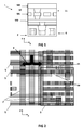
FIG 1 shows an exemplary stack of layers in an integrated circuit semiconductor device in accordance with embodiments of the present invention. -
FIG 2 shows an exemplary device in accordance with embodiments of the present invention. -
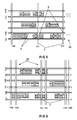
FIG 3 illustrates a prior art device in which wide power rails running perpendicular to the gate orientation are provided. -
FIG 4 illustrates the availability of routing resources for signal routing in a prior art device as also shown inFIG 3 . -
FIG 5 shows a schematic overview of an exemplary device in accordance with embodiments of the present invention. -
FIG 6 illustrates pairs of parallel power rails that alternatingly provide a supply voltage and a ground voltage in a device in accordance with embodiments of the present invention. -
FIG 7 illustrates a device in accordance with embodiments of the present invention that comprises a power rail in a third metal layer. -
FIG 8 shows a relaxed pitch in a second horizontal metal layer in a device in accordance with embodiments of the present invention. -
FIG 9 illustrates a top metal layer to provide external access to the power distribution network in a device in accordance with embodiments of the present invention. -
FIG 10 further illustrates a power distribution network extending down from a top metal layer in a flip-chip power distribution configuration, in accordance with embodiments of the present invention. -
FIG 11 shows internal power ports of the standard cells connecting directly to a vertical power rail, in a device in accordance with embodiments of the present invention. -
FIG 12 illustrates a device in accordance with embodiments of the present invention that comprises at least one power strap. - The drawings are only schematic and are non-limiting. In the drawings, the size of some of the elements may be exaggerated and not drawn on scale for illustrative purposes.
- Any reference signs in the claims shall not be construed as limiting the scope.
- In the different drawings, the same reference signs refer to the same or analogous elements.
- The present invention will be described with respect to particular embodiments and with reference to certain drawings but the invention is not limited thereto but only by the claims. The drawings described are only schematic and are non-limiting. In the drawings, the size of some of the elements may be exaggerated and not drawn on scale for illustrative purposes. The dimensions and the relative dimensions do not correspond to actual reductions to practice of the invention.
- Furthermore, the terms first, second and the like in the description and in the claims, are used for distinguishing between similar elements and not necessarily for describing a sequence, either temporally, spatially, in ranking or in any other manner. It is to be understood that the terms so used are interchangeable under appropriate circumstances and that the embodiments of the invention described herein are capable of operation in other sequences than described or illustrated herein.
- Moreover, the terms top, under and the like in the description and the claims are used for descriptive purposes and not necessarily for describing relative positions. It is to be understood that the terms so used are interchangeable under appropriate circumstances and that the embodiments of the invention described herein are capable of operation in other orientations than described or illustrated herein.
- It is to be noticed that the term "comprising", used in the claims, should not be interpreted as being restricted to the means listed thereafter; it does not exclude other elements or steps. It is thus to be interpreted as specifying the presence of the stated features, integers, steps or components as referred to, but does not preclude the presence or addition of one or more other features, integers, steps or components, or groups thereof. Thus, the scope of the expression "a device comprising means A and B" should not be limited to devices consisting only of components A and B. It means that with respect to the present invention, the only relevant components of the device are A and B.
- Reference throughout this specification to "one embodiment" or "an embodiment" means that a particular feature, structure or characteristic described in connection with the embodiment is included in at least one embodiment of the present invention. Thus, appearances of the phrases "in one embodiment" or "in an embodiment" in various places throughout this specification are not necessarily all referring to the same embodiment, but may. Furthermore, the particular features, structures or characteristics may be combined in any suitable manner, as would be apparent to one of ordinary skill in the art from this disclosure, in one or more embodiments.
- Similarly it should be appreciated that in the description of exemplary embodiments of the invention, various features of the invention are sometimes grouped together in a single embodiment, figure, or description thereof for the purpose of streamlining the disclosure and aiding in the understanding of one or more of the various inventive aspects. This method of disclosure, however, is not to be interpreted as reflecting an intention that the claimed invention requires more features than are expressly recited in each claim. Rather, as the following claims reflect, inventive aspects lie in less than all features of a single foregoing disclosed embodiment. Thus, the claims following the detailed description are hereby expressly incorporated into this detailed description, with each claim standing on its own as a separate embodiment of this invention.
- Furthermore, while some embodiments described herein include some but not other features included in other embodiments, combinations of features of different embodiments are meant to be within the scope of the invention, and form different embodiments, as would be understood by those in the art. For example, in the following claims, any of the claimed embodiments can be used in any combination.
- In the description provided herein, numerous specific details are set forth. However, it is understood that embodiments of the invention may be practiced without these specific details. In other instances, well-known methods, structures and techniques have not been shown in detail in order not to obscure an understanding of this description.
- In a first aspect, the present invention relates to an integrated circuit (IC) device comprising a stack of layers and a semiconductor substrate forming a bottom level of said stack. The IC device comprises a plurality of standard cells, in which each standard cell comprises a plurality of integrated transistors and interconnecting structures for locally interconnecting the transistors, such as to provide a predetermined function of the standard cell.
- It will be clear to the person skilled in the art that the integrated circuit device may be an integrated circuit chip, but may also relate to only a part of the integrated circuit in such integrated circuit chip. For example, an integrated circuit device in accordance with embodiments of the present invention is not necessarily limited to an entire chip device, but could be only a part of a larger integrated circuit, e.g. a subunit comprising adjacent cells, e.g. a cell row, a plurality of adjacent cell rows, a cell column, a plurality of adjacent cell columns and/or a block of adjacent standard cells. Such subunit may comprise substantially a majority of the cells in the entire device. In another part of such chip, e.g. different from a subunit in accordance with embodiments of the present invention, another power distribution network structure may be implemented, e.g. comprising a conventional power rail in a second horizontal layer. For example, the other part of the chip may have abundantly available routing resources for locally implementing the intended functionality of this other part. Such other part may for example merely implement a simple header structure. For example, in a memory chip device, the power distribution network for memory macros and logic circuits may be implemented differently, whereas the integrated circuit in accordance with embodiments of the present invention may only relate to the logic circuits (however, embodiments of the present invention relating to memory devices are not necessarily limited to only the logic circuits in such memory device). In another example, I/O pads of a mixed signal integrated circuit may have a specific power distribution network structure, as known in the art, yet such mixed signal ICs may comprise an integrated circuit device in accordance with embodiments of the present invention for implementing the logic circuitry (however, embodiments of the present invention relating to a mixed signal integrated circuit device are not necessarily limited to only the logic circuits in such mixed signal integrated circuit device).
- In other words, in an integrated circuit device in accordance with embodiments of the present invention, at least one internal power pin is comprised, in which for any conductive path in the power distribution network electrically connecting a further metal layer of the plurality of metal layers to the at least one internal power pin, any portion of this conductive path that is contained within the second horizontal metal layer covers less than the width the standard cell, as described in detail further hereinbelow. However, this does not preclude the presence of another power pin in a different part of the device, or even a further power pin in the same part of the device, that is supplied by another power distribution network structure, e.g. a conventional power distribution network, or even supplied by a part of the same power distribution network as the network supplying the at least one internal power pin.
- The predetermined function may for example comprise a primitive signal processing function, such as a logic function. The predetermined function may for example comprise a physical function, such as provided by a filler cell, a decap cell or a header cell. The predetermined function may for example comprise a signal storage function.
- The standard cells comprise parallel gate structures oriented in a first direction parallel to the substrate. The standard cell further comprises at least one internal power pin for supplying a reference voltage to contacts of the integrated transistors in accordance with the predetermined function of the standard cell. This reference voltage may relate to any or each of a plurality of reference voltages, e.g. a supply voltage and a ground voltage. For example, an internal power pin may be adapted for supplying a supply voltage and/or a ground voltage. The internal power pin may be adapted for supplying such reference voltage to source and/or drain and/or gate contacts of at least some of the integrated transistors in accordance with the predetermined function of the standard cell. However, in accordance with embodiments of the present invention, the reference voltage may equally relate to more than two reference voltages, e.g. a -5V voltage, a +3.3V voltage and a +5V voltage. A reference voltage may for example be characterized as a voltage which is not changing in time such as to encode information to be processed by the integrated circuit.
- The stack of layers further comprises a plurality of metal layers in which conductive metal lines are formed to route signals between the standard cells, e.g. to route signals between and/or inside the standard cells, the metal lines in each metal layer have a preferred orientation. Each metal layer has a preferred orientation that is orthogonal to the preferred orientation of the metal lines in an adjacent metal layer of said plurality of metal layers, e.g. a neighbouring metal layer in the stack of layers.
- It is to be understood that 'adjacent' and/or 'neighbouring' does not require that such layers are provided in direct physical contact. For example, as is known in the art, the adjacent and/or neighbouring metal layers may be separated by at least one insulating material layer, but, for example, not by an intermediate metal layer. It is also understood that such insulating material layer may be penetrated by a conductive structure, e.g. a via structure, for example to electrically connect a metal layer above the insulating material layer to a metal layer below the insulating material layer, without the conductive material layer therefore being considered as a metal layer, even if such local conductive structure comprises a metal element, as this would not be consistent with common usage and understanding of the wording 'metal layer' in the art.
- A first vertical metal layer of the plurality of metal layers is the lowest metal layer in the stack that has the first direction as preferred orientation and that provides routing resources for signal routing between the standard cells. However, signal routing in the first vertical metal layer is not necessarily limited to routing between standard cells, e.g. also intra-cell signal routing may be provided via the first vertical metal layer. For example, the first vertical metal layer may be lowest metal layer of the metal layers in the stack that satisfies simultaneously the condition of having the first direction as preferred direction and the condition of providing routing resources for signal routing between standard cells. Here, 'vertical' merely refers to the preferred orientation of this metal layer being in the first direction, which may also be referred to as the vertical direction. 'Vertical' thus does not imply a further limitation, other than the preferred orientation being in the first direction. Reference to the 'first vertical metal layer' may thus be made by simply referring to the 'first metal layer' without loss of generality. Furthermore, 'first' in the expression 'first vertical metal layer' does not imply a further limitation other than what is already implied by the layer being the lowest vertical metal layer in the stack that provides routing resources for signal routing between standard cells.
- A metal layer providing routing resources for signal routing between standard cells may refer to a metal layer comprising at least one conductive path for connecting a signal output port, e.g. a drain, source and/or gate contact, of a first standard cell to a signal input port, e.g. a drain, source and/or gate contact, of a second standard cell. Here, signal routing may refer to providing a signal that can change in time to encode information to be processed by the integrated circuit, e.g. as opposed to the reference voltage described hereinabove.
- A second horizontal metal layer of the plurality of metal layers is the nearest metal layer above the first vertical metal layer in the stack, e.g. thus having a preferred orientation in a second direction orthogonal to the first direction. Here, 'horizontal' merely refers to the preferred orientation of this metal layer being in the second direction, which may also be referred to as the horizontal direction. 'Horizontal' thus does not imply a further limitation, other than the preferred orientation being in the second direction. Reference to the 'second horizontal metal layer' may thus be made by simply referring to the 'second metal layer' without loss of generality. Furthermore, 'second' in the expression 'second horizontal metal layer' does not imply a further limitation other than what is already implied by the layer being the nearest metal layer above the first vertical metal layer in the stack. In particular embodiments of the present invention, the second horizontal metal layer may be the second metal layer, when counting from the bottom of the stack, that has the second direction as preferred direction and that provides routing resources for signal routing between the standard cells. However, this limitation is not necessarily implied for all embodiments of the present invention by merely using the wording 'second horizontal metal layer'.
- The integrated circuit device comprises a power distribution network for delivering the reference voltage, e.g. a supply voltage and/or a ground voltage, to the at least one internal power pin. For any conductive path in this power distribution network, in which this conductive path electrically connects a further metal layer of the plurality of metal layers to the at least one internal power pin, the further metal layer being arranged above the second horizontal metal layer, any portion, of this conductive path, that is contained within the second horizontal metal layer covers less than the width the standard cell in a direction orthogonal to said first direction, e.g. in the second direction, e.g. less than 75%, e.g. less than 50%, e.g. less than 25%, e.g. less than 10% of the width of the standard cell. In other words, the power distribution network may not comprise a power rail structure spanning over a plurality of standard cells in the second horizontal metal layer, e.g. over at least two standard cells, e.g. insofar relating to a part of the power distribution network supplying the reference voltage to the at least one internal pin.
- Referring to
FIG 2 , an exemplaryintegrated circuit device 1 according to embodiments of the present invention is shown. Thisintegrated circuit device 1 comprises asemiconductor substrate 2 forming a bottom level of a stack, and a plurality of layers provided on the substrate, as schematically illustrated in the cross-sectional view shown inFIG 1 . This stack may comprise at least one layer fabricated using multiple patterning. The stack may comprise at least one layer fabricated using self-aligned double patterning or self-aligned quadruple patterning. - The
IC device 1 comprises a plurality ofstandard cells 3. As known in the art, these standard cells may be arranged in at least one row, e.g. in a plurality of rows. - In accordance with embodiments of the present invention, the standard cells may be provided in a lower portion of the device that corresponds to a front-end-of-the-line portion, or to a front-end-of-the-line and middle-of-line portion, of the device. Furthermore, where is referred to a plurality of metal layers hereinbelow, the metal layers may refer to the metal layers in a back-end-of-the-line portion of the device, e.g. to the plurality of all metal layers used for signal and/or power routing in the back-of-the-line portion of the device. For example, the front-end-of-the-line portion may comprise source and drain regions of the plurality of integrated transistors and a middle-of-the-line portion may comprise a gate electrode, contact electrodes to the source and drain, a local power rail and/or other intra-cell electrically interconnecting features.
- Each
standard cell 3 comprises a plurality ofintegrated transistors 4 and interconnecting structures for locally interconnecting the transistors. For example, the standard cell may have a complementary metal oxide semiconductor architecture, comprising at least one NMOS and at least one PMOS region having transistor elements defined therein. The interconnecting structures may for example comprise conductive structures, e.g. metal structures, for directly contacting a source and/or drain region of at least one transistor. The interconnecting structures may for example comprise conductive structures, e.g. metal and/or polysilicon structures, for directly contacting a gate region of at least one transistor. The interconnecting structures may for example comprise conductive structures, e.g. metal structures, for providing single routing inside the standard cell, e.g. to connect predetermined gate, source and/or drain regions of a plurality of transistors inside the standard cell. - These integrated transistors and interconnecting structures are adapted for providing a predetermined function of the standard cell. For example, this predetermined function may comprise a primitive signal processing and/or signal storage function of the standard cell, e.g. a memory function, such as a flip-flop or latch function, or a Boolean logic function, such as an AND, OR, XOR, NAND, XNOR or inverter operation. As is known in the art, the standard cell may provide a primitive function of some complexity, e.g. a muxed D-input flipflop or a two-bit full-adder. The function of a standard cell may for example be represented by a truth table, a Boolean algebra equation, or a state transition table. However, the predetermined function may also relate to a physical function, e.g. such as to provide a header or as a filler.
- The standard cells comprise parallel gate structures oriented in a first direction parallel to the substrate, which may be referred to as a gate direction or 'vertical' direction in a plane parallel to the substrate.
- The standard cells may have a predetermined height, e.g. a height defined as a integer or non-integer multiple of tracks, in the first direction. For example, the standard cells may have a track height of 6T or 7.5T, e.g. the standard cells may be 6-track cells or 7.5-track cells.
- The standard cell further comprises at least one
internal power pin 5 for supplying a reference voltage to contacts of, e.g. of at least some of, the integrated transistors in accordance with the predetermined function of the standard cell. This reference voltage may comprise a supply voltage and/or a ground voltage. For example, at least one internal power pin may be adapted for supplying a ground voltage to at least a first contact of an integrated transistor, and at least one internal power pin may be adapted for supplying a power supply voltage to at least a second contact of an integrated transistor. Where is referred to such 'internal power pin,' this 'pin' refers to an electrical connection node, and does not imply any particular properties in terms of shape, geometry and/or size of such connector. The contacts of the integrated transistors may comprise source, drain and/or gate contacts. - In accordance with embodiments of the present invention, this at least one
internal power pin 5 may comprise a buried power rail. For example, state-of-the-art 6-track cells may comprise an outbound buried power rail to provide more available signal routing resources in the metal layers of the back-of-the-line portion of the device. - In accordance with embodiments of the present invention, this at least one
internal power pin 5 may comprise an internal power rail extending in the second direction x parallel to the substrate and orthogonal to the first direction y. This internal power rail may be provided in a local interconnect metal layer M0 of the standard cell. This interconnect metal layer M0 may refer to a middle-of-line metal layer to provide an interface between the front-end-of-the-line portion of the cell that comprises the transistors and the back-of-the-line portion of the device that interconnects the cells into an operational device. For example, the interconnect metal layer M0 may be the lowest metal layer in the stack that has the second direction x as preferred orientation and that provides routing resources for signal routing between the standard cells. However, signal routing in the interconnect metal layer M0 is not necessarily limited to routing between standard cells, e.g. also intra-cell signal routing may be provided via the interconnect metal layer M0. For example, the interconnect metal layer M0 may be the lowest metal layer in the stack that simultaneously satisfies the conditions of: having the second direction x as preferred orientation, and of providing routing resources for signal routing between the standard cells. In other words, in analogy to what was already discussed hereinabove in relation to the first vertical layer M1, the interconnect metal layer M0 may be the lowest horizontal metal layer that comprises at least one conductive path connecting a first standard cell to a second standard cell, e.g. for signal and/or power routing. For example, in 7.5-track standard cells, as known in the art, an inbound Vdd and Vss power rail may be provided in the local interconnect metal layer M0, such as to enable efficient source and drain power tapping via local interconnecting structures of the cell. - The stack of layers further comprises a plurality of metal layers in which conductive metal lines are formed to route signals between the standard cells. The metal lines in each metal layer have a preferred orientation, for example determined by a minimum spatial feature size, e.g. a pitch. For example, as known in semiconductor device fabrication, the metal layers may be fabricated such that their smallest feature size is available in only one direction. For example, the smallest trace width and spacing may be available in only the preferred direction along the plane of the metal layer. Nevertheless, due to conventional orthogonal wiring methodology, even if the smallest trace width in a metal layer can be achieved in two orthogonal directions, the metal lines in a single layer may be laid out in predominantly a single direction, the preferred direction, in which this preferred direction alternates between two perpendicular directions in the plane over neighbouring metal layers.
- Each metal layer has a preferred orientation that is orthogonal to the preferred orientation of the metal lines in an adjacent metal layer of the plurality of metal layers, e.g. the metal layers may alternate between a preferred track orientation in the first direction y and in the second direction x.
- For example, the plurality of metal layers may correspond to metal layers in a back-end-of-the-line portion of the
semiconductor device 1, while the plurality of standard cells may correspond to structures formed in a front-end-of-the-line portion, or a front-and-of-the line portion and middle-of-line portion, of thesemiconductor device 1. - A first, vertical, metal layer M1 of the plurality of metal layers is the lowest metal layer in the stack that has the first direction y as preferred orientation of the metal tracks provided therein, and that provides routing resources for signal routing between the standard cells. A second, horizontal, metal layer M2 of the plurality of metal layers is the nearest metal layer above the first, vertical, metal layer M1 in the stack. Likewise, reference to a third, vertical, metal layer M3 in present description refers to is the nearest metal layer above the second, horizontal, metal layer M2 in the stack, and reference to a fourth, horizontal, metal layer M4 in present description refers to is the nearest metal layer above the third, vertical, metal layer M3 in the stack. Likewise, in a device in accordance with embodiments of the present invention, the interconnect metal layer M0, referred to hereinabove, may be a horizontal metal layer of the plurality of metal layers that is the nearest metal layer below the first vertical metal layer M1 in the stack.
- As will be understood by the person skilled in the art, the metal layers may be separated from each other by electrically insulating
layers 11, e.g. via layers, which may be locally provided withconductive structures 12 to allow current to pass in a substantially normal direction z with respect to the substrate between the metal layers, e.g. via structures. - The integrated circuit device further comprises a power distribution network for delivering the reference voltage, e.g. a supply voltage and/or a ground voltage, e.g. Vdd and Vss, to the at least one
internal power pin 5. - Furthermore, for any conductive path in the power distribution network that electrically connects a further metal layer above the second horizontal metal layer M2 to the at least one
internal power pin 5, any portion, of such conductive path, that is entirely contained within the second horizontal metal layer M2 covers less than the width the standard cell in a direction orthogonal to said first direction y, e.g. in the second direction x, e.g. less than 75%, e.g. less than 50%, e.g. less than 25%, e.g. less than 10% of the width of the standard cell. The width of the standard cell may refer to the width of the standard cell directly underneath in a normal direction z with respect to the substrate. The width may refer to a spatial dimension in the second direction x, which is orthogonal to the first direction y and the normal direction z. - Where in conventional circuit designs known in the art at least one power rail, e.g. a power rail for Vdd and a power rail for Vss, may be provided in such second horizontal metal layer M2, this has the disadvantage of consuming a substantial amount of routing resources. Furthermore, design rules, e.g. self-aligned quadruple patterning rules, may restrict the track width of such power rails, e.g. to 3 CD, such that optimization of the routing design can be difficult in such prior art arrangements.
- For example, in an arrangement where the transistor gates of the standard cells are oriented along the first direction y, device ports may be preferably accessed via signal tracks along the second direction x, parallel to the substrate and perpendicular to the first direction y. In standard cells having a small track height, e.g. less than 9 tracks in height, port access to gate, source and/or drain regions of the transistor devices along the second direction x may be difficult in devices as known in the art due to power rails provided on the first back-of-the-line metal level with preferred direction along this second direction x, e.g. in the second horizontal metal layer M2. This may imply a disadvantageously large chip size, which may be avoided by a device in accordance with embodiments of the present invention.
- A power distribution network in an integrated circuit device according to embodiments of the present invention may comprise at least one
power rail 7 oriented along the first direction y and provided in the first vertical metal layer M1. This at least onepower rail 7 may be formed over a plurality of the standard cells, e.g. such as to cover multiple rows of standard cells. - For example, as illustrated in
FIG 2 , the at least oneinternal power pin 5 may comprise at least one internal power rail, oriented in the direction x, that is provided in a local interconnect metal layer M0 of the standard cell. Such internal power rail(s) may form the lowest level of power distribution in the semiconductor device, e.g. before connecting via branch connections to the semiconductor drain and/or source regions of the standard cell. - The
internal power pin 5, e.g. an internal power rail, may be connected, e.g. by a via connection, to at least onepower rail 7 oriented along the first direction y and provided in the first vertical metal layer M1. This at least onepower rail 7 may be formed over a plurality of the standard cells, e.g. such as to cover multiple rows of standard cells. Thus, power may be transferred, as indicated by thebold arrows 6, from the vertical rails in M1 to the internal power rails in M0. Thus, the tracks in the second horizontal metal layer M2 may be used to a large extend, e.g. exclusively, for signal routing, as opposed to power distribution. However, short metal connections may be provided in M2, e.g. such as to stitch power connection using short straps, e.g. to provide power staples, for power routing, e.g. such as cover less than the width of the standard cell by such local power connection, e.g. power straps, in M2. - A further schematic overview of the exemplary device in accordance with embodiments of the present invention, that was also shown in
FIG 2 , is provided inFIG 5 . For example, the at least onepower rail 7 in the first vertical metal layer M1 may comprise parallel power rails that alternatingly provide a supply voltage and a ground voltage, e.g. Vdd and Vss. Likewise, the at least oneinternal power pin 5 may comprise an internal power rail in the local interconnect layer M0, e.g. parallel internal power rails in M0 that alternatingly provide the supply voltage and the ground voltage. Vias 9 may connect the power rails 7 in the first vertical metal layer M1 tointernal power pins 5, e.g. the internal power rails in the local interconnect layer M0, for example such as to connect rails in M1 and M0 that carry the same voltage. - For example, as shown in
FIG 4 , in a prior-art power grid arrangement, only 5 of the 7.5 M2 tracks 31, provided in a 7.5-track standard cell architecture, may be free for signal routing, while the rest is used for power routing. For example, the available M2 tracks for signal routing are indicated by the dashedlines 33 inFIG 4 . On the other hand, only a small portion of the M1 routing resources are used byM1 straps 32 for power stitching. - However, in a device in accordance with embodiments of the present invention, substantially all M2 tracks may be available for signal routing, as indicated by the dashed
lines 35 inFIG 5 . However, more routing resources may thus be consumed by power routing in the first vertical metal layer M1. Nevertheless, as explained hereinabove, due to the gate orientation in the devices, access to source, drain and/or gate ports in the standard cell may preferably be arranged in a direction perpendicular to the gate orientation for efficiency and ease of access. - In accordance with embodiments of the present invention, the power distribution network may comprise at least one
power rail 39 oriented along the first direction and provided in a third metal layer M3 of the plurality of metal layers, as illustrated inFIG 7 . This may provide the next level of power distribution above the first vertical metal layer M1, or even the first level of power distribution above theinternal power pin 5, e.g. above an internal power rail in M0. - For example, in an integrated circuit device according to embodiments of the present invention, the power distribution network may comprise at least one power staple in the second horizontal metal layer M2 for electrically connecting a power rail in the third metal layer M3 to a power rail in the first vertical metal layer M1.
- In order to advantageously make more routing resources available for signal routing in the first vertical metal layer M1, in addition to an efficient use of routing resources in the second horizontal metal layer M2 in accordance with embodiments of the present invention, the at least one
power rail 39 oriented along the first direction and provided in the third metal layer M3 of the plurality of metal layers may be connected, e.g. by a via stack, directly to theinternal power pin 5, e.g. to internal power rails, e.g. to internal power rails in the local interconnect layer M0. - Furthermore, power straps 38 may be provided in the first vertical metal layer M1, e.g. to achieve a lower IR-drop, as shown in
FIG 7 . - Furthermore, the at least one
power rail 7, e.g. in the first vertical metal layer M1, may comprise pairs of parallel power rails that alternatingly provide a supply voltage and a ground voltage, e.g. Vdd and Vss, as shown inFIG 6 . For example, two power rails of apair 37 ofpower rails 7 in the first vertical metal layer M1 may be adapted for supplying the same voltage, in which the two power rails of the pair are adjacent, while the voltage carried by neighbouringpairs 37 may alternate between a supply voltage and a ground voltage. Thus, by doubling the power supply in the first vertical metal layer M1, advantageously the impact of static noise and dynamic voltage drops, e.g. IR and EM noise. - In an integrated circuit device in accordance with embodiments of the present invention, the power distribution network may comprise at least one
power strap 101, e.g. as shown inFIG 12 . This at least onepower strap 101 may be oriented along the second direction x, and may be provided in a horizontal metal layer above the first vertical metal layer M1, e.g. in the second horizontal metal layer M2. This at least onepower strap 101 may be adapted for locally connecting, e.g. electrically interconnecting, twopower rails 102 that are oriented along the first direction y and provided in the first vertical metal layer M1. The, or each, at least one power strap may for example electrically connect at most four power rails oriented along the first direction and provided in the first vertical metal layer. The, or each, at least one power strap may for example electrically connect at most two power rails oriented along the first direction and provided in the first vertical metal layer. These at most two power rails may, for example, be two adjacent, e.g. neighboring, power rails for carrying the same reference voltage. - The at least one power strap may form part of a conductive path electrically connecting a further metal layer above the second horizontal metal layer to the at least one internal power pin. Alternatively, the at least one power strap may form part of a conductive path electrically connecting a further metal layer above the second horizontal metal layer to a further internal power pin.
- For example, an integrated circuit device in accordance with embodiments of the present invention may comprise at least one further standard cell that comprises a plurality of integrated transistors and interconnecting structures for locally interconnecting the transistors such as to provide a predetermined function of the further standard cell. The further standard cells may comprise parallel gate structures oriented in the first direction. The further standard cell may comprise at least one further internal power pin, e.g. a power connector that is internal in the further standard cell, for supplying a reference voltage to contacts of the integrated transistors in accordance with the predetermined function of the further standard cell. Likewise as discussed in present description in relation to the at least one
internal power pin 5, the at least one further power pin may comprise an internal power rail, e.g. in the local interconnect layer M0, and/or a buried power rail. - The power distribution network may be adapted for delivering the reference voltage to the at least one further internal power pin. The, e.g. each, at least one power strap may form part of a conductive path electrically connecting a further metal layer above the second horizontal metal layer to the at least one further internal power pin. The at least one power strap may have a length that covers less than 129 times the width of the further standard cell in said second direction, e.g. less than 65 times the width of the further standard cell, e.g. less than 33 times the width of the further standard cell, e.g. less than 17 times the width of the further standard cell, e.g. less than five times said width, e.g. less than four times said width, e.g. preferably less than three times said width, e.g. even more preferable less than twice said width, e.g. having a length that does not exceed 150% of the width of the further standard cell, e.g. having a length less than or equal to 125% of the width of the further standard cell. The at least one power strap may have a length that covers less than an entire cell row of the integrated circuit device, e.g. preferably less than or equal to 50% of the entire cell row, e.g. less than or equal to 25% of the entire cell row, e.g. even more preferred less than or equal to 10% of the entire cell row, e.g. less than or equal to 5% of the entire cell row.
- It is an advantage of such power strap arrangement in a device in accordance with embodiments of the present invention that locally a low resistance, and thus a low IR drop can be achieved, and/or that locally a low current density of a power supply current can be achieved, e.g. to achieve a low electromigration (EM). This may be particularly advantageous to prevent hotspot formation, e.g. for IR or EM. Thus, even where an advantageous increase in free routing resources, as compared to particular prior art devices, can be achieved by short power routing paths in the second horizontal metal layer M2 in accordance with embodiments of the present invention, an extended power strap may be provided locally in the second horizontal metal layer M2 to prevent hotspots. However, such extended power strap may still be relatively short, such as to prevent a blocking allocation of routing resources over a large area of the device, e.g. an entire cell row.
- In accordance with embodiments of the present invention, the second horizontal metal layer M2 may have a larger pitch, e.g. center-to-center distance in the first direction y between the interconnect lines, than the smallest pitch of the other metal layers in the stack, e.g. than the smallest (or tightest) pitch of the other horizontal metal layers in the stack, or than the smallest (or tightest) pitch of the vertical metal layers in the stack.
- For example, while the standard cell may be a 6-track cell, e.g. having a cell height of 192 nm, e.g. using 32 nm process technology, the second horizontal metal layer M2 may have a higher pitch, e.g. providing 4 tracks per row, e.g. corresponding to a 48 nm pitch. In accordance with embodiments of the present invention, the second horizontal metal layer M2 may have a relaxed pitch. As shown in
FIG 8 , where in a conventional power distribution network as known in the art for such 6-track cell with 4-track M2 pitch, two M2 tracks may be reserved for power rails and only twotracks 42 would be available for signal routing, in accordance with embodiments of the present invention, 4 M2 tracks may be available for signal routing. - In accordance with embodiments of the present invention, about 20% utilization gain may be achievable when compared to a similar device using M2 power rails as known in the art. Furthermore, by relaxing the pitch of the second, horizontal, metal layer M2, a reduced cost may be achieved, as well as advantageous improvement of capacitance and/or resistance. Furthermore, it is an advantage that good and efficient pin pickup may be achieved.
- An
integrated circuit device 1 in accordance with embodiments of the present invention may comprise atop metal layer 50, e.g. a back metal layer forming top level of the stack, that provides external access to the power distribution network, as shown inFIG 9 . - This
top metal layer 50 may also provide external access to signal lines extending through the metal layers to input and/or output ports of the standard cells. The top metal layer may comprise a flip chip region in which access pads are provided for the power distribution network to power and ground voltage supplies in a regular, two-dimensional grid pattern. For example,access pads 54 for the power voltage supply may form aneffective mesh 53 that is diagonally offset with respect aneffective mesh 51 formed byaccess pads 52 for the ground supply voltage, as is known in the art. The access pads in this flip chip region may be provided with apredetermined pad pitch 55, e.g. of 150 µm, in a two-dimensional regular grid. - As shown in
FIG 10 , the power distribution network may extend down from thetop metal layer 50 in a power distribution configuration, similar to flip chip power supply networks as known in the art. However, at the lower levels of this network, the power may be supplied in accordance with embodiments of the present invention, for example to power rails in the first vertical metal layer M1 which run along the first direction y, from which power ports of the standard cells may be tapped further below, e.g. via theinternal power pins 5, e.g. via internal power rails in the interconnect metal layer M0. - For example, a higher portion of the power distribution network may distribute the power and ground voltage supplied via the
top metal layer 50 over power and ground power rail pairs at apredetermined pitch 58, which is typically larger, e.g. substantially larger, than the standard cell height and width. Further down, each power and ground pair may be distributed by a lower portion of the power distribution network that provides connections to the lowest level of power rails above the intra-cell level, e.g. to power rails in the first vertical metal layer M1, at a predetermined power to groundpitch 57, which may, for example, typically correspond to the width of about 8 standard cells. Thus, the lower metal resistive mesh can be sparse. In a device as known in the art, vertical power rails in the third metal layer M3 may cross and connect to horizontal power rails in the metal layer M2. Each row of standard cells may be powered in a prior-art device by a corresponding ground power rail and a corresponding supply voltage power rail in the metal layer M2. However, as shown inFIG 11 , in a device in accordance with embodiments of the present invention, internal power ports of the standard cells in arow 61, e.g. power ports on aninternal power rail 5, may connect directly to a vertical power rail in the metal layers, e.g. to a power rail provided in the first vertical metal layer M1. - In a second aspect, the present invention also relates to a method for manufacturing an integrated circuit device, e.g. an integrated circuit device in accordance with embodiments of the first aspect of the present invention. This method comprises providing a stack of layers and a semiconductor substrate forming a bottom level of this stack, e.g. providing the semiconductor substrate and a plurality of layers thereon such as to form a stack. The method also comprises fabricating a plurality of standard cells, in which each standard cell comprises a plurality of integrated transistors and interconnecting structures for locally interconnecting the transistors such as to provide a predetermined function of the standard cell. The standard cells are fabricated such that the standard cells comprise parallel gate structures oriented in a first direction parallel to the substrate. Each standard cell is manufactured such as to comprise at least one internal power pin for supplying a reference voltage to contacts of the integrated transistors in accordance with the predetermined function of the standard cell. This at least one internal power pin may be manufactured in a front-end-of-the-line process and/or a middle-of-line process.
- Furthermore, providing the stack of layers comprises providing a plurality of metal layers in which conductive metal lines are formed to route signals between said standard cells, e.g. to provide signal routing between the standard cells. The metal lines in each metal layer are providing to have a preferred orientation, in which each metal layer has a preferred orientation that is orthogonal to the preferred orientation of the metal lines in an adjacent metal layer of the plurality of metal layers.
- A first vertical metal layer M1 of the plurality of metal layers is furthermore provided as the lowest metal layer in the stack that has the first direction as preferred orientation and that provides routing resources for signal routing between the standard cells. A second horizontal metal layer M2 of the plurality of metal layers is provided as the nearest metal layer above the first vertical metal layer M1 in the stack.
- The method furthermore comprises providing a power distribution network for delivering the reference voltage, e.g. a supply voltage and a ground voltage, to the at least one internal power pin, e.g. to an internal power rail, such that, for any conductive path in the power distribution network that electrically connects a further metal layer above the second horizontal metal layer M2 to the at least one internal power pin, any portion, of such conductive path, that is contained within the second horizontal metal layer M2 covers less than the width of the standard cell in a second direction orthogonal to the first direction. These and other features of a method in accordance with embodiments of the second aspect of the present invention may be understood by the skilled person from the description provided hereinabove relating to embodiments of the first aspect of the present invention.
- In a method in accordance with embodiments of the present invention, fabricating the plurality of standard cells may comprise providing an internal power rail extending in the second direction, in which this internal power rail is provided in a local interconnect metal layer M0 of the standard cells.
- In a method in accordance with embodiments of the present invention, fabricating the plurality of standard cells may comprise providing a buried power rail.
- In a method in accordance with embodiments of the present invention, providing the power distribution network may comprise providing at least one power rail, oriented along the first direction, in the first vertical metal layer M1.
- In a method in accordance with embodiments of the present invention, providing the power distribution network may comprise providing at least one power rail, oriented along the first direction, in a third metal layer M3 of the plurality of metal layers, wherein this third metal layer M3 is the nearest metal layer above the second horizontal metal layer M2 in the stack.
- In a method in accordance with embodiments of the present invention, providing the power distribution network may comprise providing at least one power staple in the second horizontal metal layer M2 for electrically connecting the power rail in the third vertical metal layer M3 to the
power rail 7 in the first vertical metal layer M1.
Claims (15)
- An integrated circuit device (1) comprising a stack of layers and a semiconductor substrate (2) forming a bottom level of said stack;
said integrated circuit device comprising a plurality of standard cells (3), each standard cell comprising a plurality of integrated transistors (4) and interconnecting structures for locally interconnecting said transistors such as to provide a predetermined function of said standard cell (3);
said standard cells (3) comprising parallel gate structures oriented in a first direction (y) parallel to said substrate (2);
said standard cell comprising at least one internal power pin (5) for supplying a reference voltage to contacts of said integrated transistors in accordance with said predetermined function of the standard cell;
said stack of layers further comprising a plurality of metal layers in which conductive metal lines are formed to route signals between said standard cells (3), said metal lines in each metal layer having a preferred orientation, in which each metal layer has a preferred orientation that is orthogonal to the preferred orientation of the metal lines in an adjacent metal layer of said plurality of metal layers;
wherein a first vertical metal layer (M1) of said plurality of metal layers is the lowest metal layer in said stack that has said first direction (y) as preferred orientation and that provides routing resources for signal routing between said standard cells,, and wherein a second horizontal metal layer (M2) of said plurality of metal layers is the nearest metal layer above the first vertical metal layer (M1) in said stack;
said integrated circuit device further comprising a power distribution network for delivering said reference voltage to said at least one internal power pin (5);
wherein for any conductive path in said power distribution network that electrically connects a further metal layer above said second horizontal metal layer (M2) to said at least one internal power pin (5), any portion, of said conductive path, that is contained within the second horizontal metal layer (M2) covers less than the width of the standard cell in a second direction (x) orthogonal to said first direction (y). - The integrated circuit device according to claim 1, wherein said at least one internal power pin (5) comprises a buried power rail.
- The integrated circuit device according to claim 1 or claim 2, wherein said at least one internal power pin (5) comprises an internal power rail extending in said second direction (x), said internal power rail being provided in a local interconnect metal layer (M0) of said standard cells.
- The integrated circuit device according to any of the previous claims, in which said stack comprises at least one layer fabricated using multiple patterning.
- The integrated circuit device according to claim 4, wherein said at least one layer is fabricated using self-aligned double patterning or self-aligned quadruple patterning.
- The integrated circuit device according to any of the previous claims, in which said power distribution network comprises at least one power rail (7) oriented along said first direction (y) and provided in said first vertical metal layer (M1).
- The integrated circuit device according to any of the previous claims, in which said power distribution network comprises at least one power rail oriented along said first direction (y) and provided in a third vertical metal layer (M3) of said plurality of metal layers, wherein said third vertical metal layer (M3) is the nearest metal layer above the second horizontal metal layer (M2) in said stack.
- The integrated circuit device according to claims 6 and 7, in which said power distribution network comprises at least one power staple in said second horizontal metal layer (M2) for electrically connecting said power rail in said third vertical metal layer (M3) to said power rail in said first vertical metal layer (M1).
- The integrated circuit device according to any of the previous claims, in which said power distribution network comprises at least one power strap (101) oriented along said second direction (x) and provided in a horizontal metal layer above the first vertical metal layer (M1) such as to locally connect two power rails (102) oriented along said first direction (y), said two power rails (102) being provided in said first vertical metal layer (M1).
- The integrated circuit device according to any of the previous claims, wherein said second horizontal metal layer (M2) has a larger pitch than the smallest pitch of the other metal layers in said stack.
- A method for manufacturing an integrated circuit device (1), the method comprising- providing a stack of layers on a semiconductor substrate (2), and- fabricating a plurality of standard cells (3), each standard cell comprising a plurality of integrated transistors (4) and interconnecting structures for locally interconnecting said transistors such as to provide a predetermined function of said standard cell (3), said standard cells (3) comprising parallel gate structures oriented in a first direction (y) parallel to said substrate (2), said standard cell comprising at least one internal power pin (5) for supplying a reference voltage to contacts of said integrated transistors in accordance with said predetermined function of the standard cell;wherein providing said stack of layers comprises providing a plurality of metal layers in which conductive metal lines are formed to route signals between said standard cells (3), said metal lines in each metal layer having a preferred orientation, in which each metal layer has a preferred orientation that is orthogonal to the preferred orientation of the metal lines in an adjacent metal layer of said plurality of metal layers;
wherein a first vertical metal layer (M1) of said plurality of metal layers is provided as the lowest metal layer in said stack that has said first direction (y) as preferred orientation and that provides routing resources for signal routing between said standard cells, and wherein a second horizontal metal layer (M2) of said plurality of metal layers is provided as the nearest metal layer above the first vertical metal layer (M1) in said stack;
the method furthermore comprising providing a power distribution network for delivering said reference voltage to said at least one internal power pin, such that, for any conductive path in said power distribution network that electrically connects a further metal layer above said second horizontal metal layer (M2) to said at least one internal power pin (5), any portion, of said conductive path, that is contained within the second horizontal metal layer (M2) covers less than the width of the standard cell in a second direction (x) orthogonal to said first direction (y). - The method according to claim 11, wherein fabricating the plurality of standard cells comprises providing an internal power rail extending in said second direction (x), said internal power rail being provided in a local interconnect metal layer (M0) of said standard cells.
- The method according to claim 11 or 12, wherein providing said power distribution network comprises providing at least one power rail (7), oriented along said first direction (y), in said first vertical metal layer (M1).
- The method according to any of claims 11 to 13, wherein providing said power distribution network comprises providing at least one power rail, oriented along said first direction (y), in a third vertical metal layer (M3) of said plurality of metal layers, wherein said third vertical metal layer (M3) is the nearest metal layer above the second horizontal metal layer (M2) in said stack.
- The method according to claim 14 and claim 13, in which providing said power distribution network comprises providing at least one power staple in said second horizontal metal layer (M2) for electrically connecting said power rail in said third vertical metal layer (M3) to said power rail (7) in said first vertical metal layer (M1).
Priority Applications (2)
| Application Number | Priority Date | Filing Date | Title |
|---|---|---|---|
| EP16164134.5A EP3229270A1 (en) | 2016-04-06 | 2016-04-06 | Integrated circuit power distribution network |
| US15/479,633 US10510774B2 (en) | 2016-04-06 | 2017-04-05 | Integrated circuit power distribution network |
Applications Claiming Priority (1)
| Application Number | Priority Date | Filing Date | Title |
|---|---|---|---|
| EP16164134.5A EP3229270A1 (en) | 2016-04-06 | 2016-04-06 | Integrated circuit power distribution network |
Publications (1)
| Publication Number | Publication Date |
|---|---|
| EP3229270A1 true EP3229270A1 (en) | 2017-10-11 |
Family
ID=55750312
Family Applications (1)
| Application Number | Title | Priority Date | Filing Date |
|---|---|---|---|
| EP16164134.5A Pending EP3229270A1 (en) | 2016-04-06 | 2016-04-06 | Integrated circuit power distribution network |
Country Status (2)
| Country | Link |
|---|---|
| US (1) | US10510774B2 (en) |
| EP (1) | EP3229270A1 (en) |
Cited By (8)
| Publication number | Priority date | Publication date | Assignee | Title |
|---|---|---|---|---|
| WO2019139705A1 (en) * | 2018-01-10 | 2019-07-18 | Qualcomm Incorporated | POWER DISTRIBUTION NETWORKS (PDNs) USING HYBRID GRID AND PILLAR ARRANGEMENTS |
| WO2019165087A1 (en) * | 2018-02-22 | 2019-08-29 | Xilinx, Inc. | Power distribution for active-on-active die stack with reduced resistance |
| CN111128997A (en) * | 2018-10-31 | 2020-05-08 | 台湾积体电路制造股份有限公司 | Method for generating integrated circuit layout |
| CN111684589A (en) * | 2018-02-02 | 2020-09-18 | Arm 有限公司 | distribution circuit |
| CN113451264A (en) * | 2020-03-24 | 2021-09-28 | 瑞昱半导体股份有限公司 | Integrated circuit device |
| WO2021255570A1 (en) * | 2020-06-18 | 2021-12-23 | International Business Machines Corporation | Sloped epitaxy buried contact |
| US12277375B2 (en) | 2022-01-27 | 2025-04-15 | International Business Machines Corporation | Power staple avoidance for routing via reduction |
| US12575399B2 (en) | 2022-01-26 | 2026-03-10 | International Business Machines Corporation | Interconnect structure including vertically stacked power and ground lines |
Families Citing this family (47)
| Publication number | Priority date | Publication date | Assignee | Title |
|---|---|---|---|---|
| US10127340B2 (en) * | 2016-09-30 | 2018-11-13 | Taiwan Semiconductor Manufacturing Company, Ltd. | Standard cell layout, semiconductor device having engineering change order (ECO) cells and method |
| US11347925B2 (en) * | 2017-05-01 | 2022-05-31 | Advanced Micro Devices, Inc. | Power grid architecture and optimization with EUV lithography |
| US11211330B2 (en) | 2017-05-01 | 2021-12-28 | Advanced Micro Devices, Inc. | Standard cell layout architectures and drawing styles for 5nm and beyond |
| US10878163B2 (en) * | 2017-08-30 | 2020-12-29 | Taiwan Semiconductor Manufacturing Company, Ltd. | Semiconductor device including PG-aligned cells and method of generating layout of same |
| WO2019048028A1 (en) | 2017-09-05 | 2019-03-14 | Huawei Technologies Co., Ltd. | Optical transmitter and transmission method |
| TWI636542B (en) | 2017-10-20 | 2018-09-21 | 智原科技股份有限公司 | Integrated circuit distribution network |
| US10790273B2 (en) | 2017-12-07 | 2020-09-29 | Samsung Electronics Co., Ltd. | Integrated circuits including standard cells and method of manufacturing the integrated circuits |
| US10916498B2 (en) | 2018-03-28 | 2021-02-09 | Taiwan Semiconductor Manufacturing Co., Ltd. | Interconnect structure for logic circuit |
| US10366954B1 (en) | 2018-04-25 | 2019-07-30 | Globalfoundries Inc. | Structure and method for flexible power staple insertion |
| US10748889B2 (en) | 2018-06-15 | 2020-08-18 | Samsung Electronics Co., Ltd. | Power grid and standard cell co-design structure and methods thereof |
| US10867102B2 (en) * | 2018-06-28 | 2020-12-15 | Taiwan Semiconductor Manufacturing Company, Ltd. | Inverted pitch IC structure, layout method, and system |
| US10607982B2 (en) * | 2018-07-10 | 2020-03-31 | Samsung Electronics Co., Ltd. | Layout connection isolation technique for improving immunity to jitter and voltage drop in a standard cell |
| US11017146B2 (en) * | 2018-07-16 | 2021-05-25 | Taiwan Semiconductor Manufacturing Company, Ltd. | Integrated circuit and method of forming the same |
| CN109326578B (en) * | 2018-09-07 | 2021-02-26 | 上海兆芯集成电路有限公司 | Power supply network and wiring method thereof |
| KR102576212B1 (en) | 2018-09-21 | 2023-09-07 | 삼성전자주식회사 | Semiconductor devices |
| US10872818B2 (en) | 2018-10-26 | 2020-12-22 | Taiwan Semiconductor Manufacturing Company, Ltd. | Buried power rail and method forming same |
| US11195797B2 (en) | 2019-05-21 | 2021-12-07 | Samsung Electronics Co., Ltd. | Applications of buried power rails |
| US10886224B2 (en) | 2019-05-22 | 2021-01-05 | Samsung Electronics Co., Ltd. | Power distribution network using buried power rail |
| JP7268728B2 (en) | 2019-05-23 | 2023-05-08 | 株式会社ソシオネクスト | semiconductor equipment |
| WO2020235084A1 (en) | 2019-05-23 | 2020-11-26 | 株式会社ソシオネクスト | Semiconductor device |
| US11233008B2 (en) | 2019-06-19 | 2022-01-25 | Samsung Electronics Co., Ltd. | Method of manufacturing an integrated circuit with buried power rail |
| US10796061B1 (en) | 2019-08-29 | 2020-10-06 | Advanced Micro Devices, Inc. | Standard cell and power grid architectures with EUV lithography |
| US11449116B2 (en) * | 2019-09-26 | 2022-09-20 | Arm Limited | Power grid porosity techniques |
| US11756876B2 (en) * | 2020-04-01 | 2023-09-12 | Taiwan Semiconductor Manufacturing Company Ltd. | Semiconductor devices having power rails and signal tracks arranged in different layer |
| KR102899035B1 (en) * | 2020-04-29 | 2025-12-12 | 삼성전자주식회사 | Semiconductor devices |
| US11222831B2 (en) | 2020-06-04 | 2022-01-11 | Samsung Electronics Co., Ltd. | Stacked integrated circuit devices |
| US11296070B2 (en) * | 2020-06-12 | 2022-04-05 | Taiwan Semiconductor Manufacturing Company Limited | Integrated circuit with backside power rail and backside interconnect |
| US11961802B2 (en) * | 2020-12-04 | 2024-04-16 | Tokyo Electron Limited | Power-tap pass-through to connect a buried power rail to front-side power distribution network |
| US12148697B2 (en) * | 2020-12-17 | 2024-11-19 | Arm Limited | Devices and methods of local interconnect stitches and power grids |
| JP7635557B2 (en) * | 2021-01-19 | 2025-02-26 | 株式会社ソシオネクスト | Semiconductor Device |
| EP4274309A4 (en) * | 2021-03-24 | 2024-07-17 | Samsung Electronics Co., Ltd. | ELECTRONIC DEVICE FOR CARRYING OUT A NETWORK MANAGEMENT OPERATION, AND ASSOCIATED OPERATING METHOD |
| US20220328409A1 (en) * | 2021-04-08 | 2022-10-13 | Taiwan Semiconductor Manufacturing Company, Ltd. | Targeted power grid structure and method |
| KR102957844B1 (en) | 2021-05-06 | 2026-04-29 | 삼성전자주식회사 | Semiconductor devices and manufacturing method of the same |
| US11984384B2 (en) | 2021-09-09 | 2024-05-14 | Synopsys, Inc. | Power routing for 2.5D or 3D integrated circuits including a buried power rail and interposer with power delivery network |
| US12205897B2 (en) | 2021-09-23 | 2025-01-21 | Advanced Micro Devices, Inc. | Standard cell design architecture for reduced voltage droop utilizing reduced contacted gate poly pitch and dual height cells |
| US11990412B2 (en) * | 2021-09-29 | 2024-05-21 | International Business Machines Corporation | Buried power rails located in a base layer including first, second, and third etch stop layers |
| EP4199052B1 (en) * | 2021-12-17 | 2024-08-21 | IMEC vzw | Metallization scheme for an integrated circuit |
| US20230197612A1 (en) * | 2021-12-20 | 2023-06-22 | Intel Corporation | Backside power delivery network and signal routing |
| EP4199090A1 (en) * | 2021-12-20 | 2023-06-21 | Imec VZW | Multiport sram in sequential 3d technology |
| US12598979B2 (en) | 2022-03-21 | 2026-04-07 | Apple Inc. | Dual contact and power rail for high performance standard cells |
| US12543555B2 (en) | 2022-03-21 | 2026-02-03 | Apple Inc. | Backside routing implementation in SRAM arrays |
| US12271674B2 (en) | 2022-03-23 | 2025-04-08 | International Business Machines Corporation | Generating a power delivery network based on the routing of signal wires within a circuit design |
| KR102949453B1 (en) | 2022-05-19 | 2026-04-07 | 삼성전자주식회사 | Semiconductor devices |
| CN114864525B (en) * | 2022-07-08 | 2022-10-21 | 之江实验室 | Standard integrated area wiring structure and method of wafer substrate suitable for on-chip integration |
| US12511463B2 (en) | 2022-08-31 | 2025-12-30 | Apple Inc. | Backside contacts for signal routing |
| CN118824990A (en) * | 2023-04-17 | 2024-10-22 | 联华电子股份有限公司 | Semiconductor structure |
| US20250273573A1 (en) * | 2023-10-02 | 2025-08-28 | Taiwan Semiconductor Manufacturing Company, Ltd. | Integrated circuit and method of forming the same |
Citations (5)
| Publication number | Priority date | Publication date | Assignee | Title |
|---|---|---|---|---|
| US20100097875A1 (en) * | 2008-10-20 | 2010-04-22 | David Vinke | Enhanced Power Distribution in an Integrated Circuit |
| US20130063203A1 (en) * | 2011-09-08 | 2013-03-14 | Kabushiki Kaisha Toshiba | Semiconductor integrated circuit, design method of same, and design apparatus of same |
| US20140175565A1 (en) * | 2007-03-05 | 2014-06-26 | Tela Innovations, Inc. | Integrated Circuit Cell Library for Multiple Patterning |
| US20140229908A1 (en) * | 2011-03-03 | 2014-08-14 | Synopsys, Inc. | Power Routing in Standard Cells |
| US20150357282A1 (en) * | 2014-06-10 | 2015-12-10 | Vincent Chun Fai LAU | Logic cell, semiconductor device including logic cell, and method of manufacturing the logic cell and semiconductor device |
Family Cites Families (4)
| Publication number | Priority date | Publication date | Assignee | Title |
|---|---|---|---|---|
| US5742099A (en) * | 1994-09-29 | 1998-04-21 | Intel Corporation | Power bus for an integrated circuit including end-to-end arranged segments providing power and ground |
| CN100468735C (en) * | 2006-08-25 | 2009-03-11 | 威盛电子股份有限公司 | Power ground network for integrated circuit and arrangement method thereof |
| FI125245B (en) * | 2009-03-12 | 2015-07-31 | Aker Arctic Technology Inc | Vessels or floating construction operating in iced water and operating procedures therefore |
| JP5741234B2 (en) * | 2011-06-10 | 2015-07-01 | 富士通株式会社 | Cell arrangement structure, semiconductor integrated circuit, and circuit element cell arrangement method |
-
2016
- 2016-04-06 EP EP16164134.5A patent/EP3229270A1/en active Pending
-
2017
- 2017-04-05 US US15/479,633 patent/US10510774B2/en active Active
Patent Citations (5)
| Publication number | Priority date | Publication date | Assignee | Title |
|---|---|---|---|---|
| US20140175565A1 (en) * | 2007-03-05 | 2014-06-26 | Tela Innovations, Inc. | Integrated Circuit Cell Library for Multiple Patterning |
| US20100097875A1 (en) * | 2008-10-20 | 2010-04-22 | David Vinke | Enhanced Power Distribution in an Integrated Circuit |
| US20140229908A1 (en) * | 2011-03-03 | 2014-08-14 | Synopsys, Inc. | Power Routing in Standard Cells |
| US20130063203A1 (en) * | 2011-09-08 | 2013-03-14 | Kabushiki Kaisha Toshiba | Semiconductor integrated circuit, design method of same, and design apparatus of same |
| US20150357282A1 (en) * | 2014-06-10 | 2015-12-10 | Vincent Chun Fai LAU | Logic cell, semiconductor device including logic cell, and method of manufacturing the logic cell and semiconductor device |
Cited By (14)
| Publication number | Priority date | Publication date | Assignee | Title |
|---|---|---|---|---|
| US10380308B2 (en) | 2018-01-10 | 2019-08-13 | Qualcomm Incorporated | Power distribution networks (PDNs) using hybrid grid and pillar arrangements |
| CN111602243B (en) * | 2018-01-10 | 2024-06-11 | 高通股份有限公司 | Power distribution network (PDN) using hybrid grid and pillar arrangements |
| WO2019139705A1 (en) * | 2018-01-10 | 2019-07-18 | Qualcomm Incorporated | POWER DISTRIBUTION NETWORKS (PDNs) USING HYBRID GRID AND PILLAR ARRANGEMENTS |
| CN111602243A (en) * | 2018-01-10 | 2020-08-28 | 高通股份有限公司 | Power Distribution Network (PDN) using hybrid grid and post arrangements |
| CN111684589A (en) * | 2018-02-02 | 2020-09-18 | Arm 有限公司 | distribution circuit |
| US11670585B1 (en) | 2018-02-22 | 2023-06-06 | Xilinx, Inc. | Power distribution for active-on-active die stack with reduced resistance |
| US11041211B2 (en) | 2018-02-22 | 2021-06-22 | Xilinx, Inc. | Power distribution for active-on-active die stack with reduced resistance |
| WO2019165087A1 (en) * | 2018-02-22 | 2019-08-29 | Xilinx, Inc. | Power distribution for active-on-active die stack with reduced resistance |
| CN111128997A (en) * | 2018-10-31 | 2020-05-08 | 台湾积体电路制造股份有限公司 | Method for generating integrated circuit layout |
| CN113451264A (en) * | 2020-03-24 | 2021-09-28 | 瑞昱半导体股份有限公司 | Integrated circuit device |
| CN113451264B (en) * | 2020-03-24 | 2024-05-31 | 瑞昱半导体股份有限公司 | Integrated Circuit Devices |
| WO2021255570A1 (en) * | 2020-06-18 | 2021-12-23 | International Business Machines Corporation | Sloped epitaxy buried contact |
| US12575399B2 (en) | 2022-01-26 | 2026-03-10 | International Business Machines Corporation | Interconnect structure including vertically stacked power and ground lines |
| US12277375B2 (en) | 2022-01-27 | 2025-04-15 | International Business Machines Corporation | Power staple avoidance for routing via reduction |
Also Published As
| Publication number | Publication date |
|---|---|
| US20170294448A1 (en) | 2017-10-12 |
| US10510774B2 (en) | 2019-12-17 |
Similar Documents
| Publication | Publication Date | Title |
|---|---|---|
| US10510774B2 (en) | Integrated circuit power distribution network | |
| CN114631180B (en) | CFET Power Delivery Network for Buried Power Rails | |
| CN112771655B (en) | Semiconductor integrated circuit device and semiconductor package structure | |
| US11004780B2 (en) | Hard macro having blockage sites, integrated circuit including same and method of routing through a hard macro | |
| US6938226B2 (en) | 7-tracks standard cell library | |
| US6838713B1 (en) | Dual-height cell with variable width power rail architecture | |
| US20080180132A1 (en) | Semiconductor device and method of fabricating the same | |
| KR20140084017A (en) | Gate array architecture with multiple programmable regions | |
| US7760578B2 (en) | Enhanced power distribution in an integrated circuit | |
| US9337139B2 (en) | Semiconductor device having compensation capacitor to stabilize power supply voltage | |
| US12354962B2 (en) | Standard cell layout for better routability | |
| US7786566B2 (en) | Semiconductor integrated circuit | |
| JP3825252B2 (en) | Flip chip type semiconductor device | |
| CN100442497C (en) | Semiconductor device with stacked chips | |
| KR20150139435A (en) | An integrated circuit with interface circuitry, and an interface cell for such interface cicuitry | |
| JPH10284605A (en) | Semiconductor integrated circuit and semiconductor integrated circuit layout-designed by cell-based method | |
| JP6836137B2 (en) | Semiconductor device and its layout design method | |
| CN105322943B (en) | Integrated circuit with interface circuit, and interface unit for interface circuit | |
| US11621259B2 (en) | Semiconductor chip | |
| US20240347460A1 (en) | Semiconductor integrated circuit device | |
| US20250156623A1 (en) | Semiconductor integrated circuit in backside power distribution network semiconductor architecture and design method thereof | |
| WO1994029902A1 (en) | Flexcell gate array | |
| JPH03218052A (en) | Semiconductor integrated circuit device |
Legal Events
| Date | Code | Title | Description |
|---|---|---|---|
| PUAI | Public reference made under article 153(3) epc to a published international application that has entered the european phase |
Free format text: ORIGINAL CODE: 0009012 |
|
| STAA | Information on the status of an ep patent application or granted ep patent |
Free format text: STATUS: THE APPLICATION HAS BEEN PUBLISHED |
|
| AK | Designated contracting states |
Kind code of ref document: A1 Designated state(s): AL AT BE BG CH CY CZ DE DK EE ES FI FR GB GR HR HU IE IS IT LI LT LU LV MC MK MT NL NO PL PT RO RS SE SI SK SM TR |
|
| AX | Request for extension of the european patent |
Extension state: BA ME |
|
| STAA | Information on the status of an ep patent application or granted ep patent |
Free format text: STATUS: REQUEST FOR EXAMINATION WAS MADE |
|
| 17P | Request for examination filed |
Effective date: 20180409 |
|
| RBV | Designated contracting states (corrected) |
Designated state(s): AL AT BE BG CH CY CZ DE DK EE ES FI FR GB GR HR HU IE IS IT LI LT LU LV MC MK MT NL NO PL PT RO RS SE SI SK SM TR |
|
| STAA | Information on the status of an ep patent application or granted ep patent |
Free format text: STATUS: EXAMINATION IS IN PROGRESS |
|
| 17Q | First examination report despatched |
Effective date: 20201217 |