EP3226433A2 - Demodulator eines drahtloskommunikationslesers - Google Patents
Demodulator eines drahtloskommunikationslesers Download PDFInfo
- Publication number
- EP3226433A2 EP3226433A2 EP17158554.0A EP17158554A EP3226433A2 EP 3226433 A2 EP3226433 A2 EP 3226433A2 EP 17158554 A EP17158554 A EP 17158554A EP 3226433 A2 EP3226433 A2 EP 3226433A2
- Authority
- EP
- European Patent Office
- Prior art keywords
- phase
- carrier signal
- demodulator
- signal
- estimating
- Prior art date
- Legal status (The legal status is an assumption and is not a legal conclusion. Google has not performed a legal analysis and makes no representation as to the accuracy of the status listed.)
- Granted
Links
Images




Classifications
-
- H—ELECTRICITY
- H04—ELECTRIC COMMUNICATION TECHNIQUE
- H04B—TRANSMISSION
- H04B5/00—Near-field transmission systems, e.g. inductive or capacitive transmission systems
- H04B5/40—Near-field transmission systems, e.g. inductive or capacitive transmission systems characterised by components specially adapted for near-field transmission
- H04B5/48—Transceivers
-
- G—PHYSICS
- G06—COMPUTING OR CALCULATING; COUNTING
- G06K—GRAPHICAL DATA READING; PRESENTATION OF DATA; RECORD CARRIERS; HANDLING RECORD CARRIERS
- G06K7/00—Methods or arrangements for sensing record carriers, e.g. for reading patterns
- G06K7/10—Methods or arrangements for sensing record carriers, e.g. for reading patterns by electromagnetic radiation, e.g. optical sensing; by corpuscular radiation
- G06K7/10009—Methods or arrangements for sensing record carriers, e.g. for reading patterns by electromagnetic radiation, e.g. optical sensing; by corpuscular radiation sensing by radiation using wavelengths larger than 0.1 mm, e.g. radio-waves or microwaves
-
- H—ELECTRICITY
- H03—ELECTRONIC CIRCUITRY
- H03D—DEMODULATION OR TRANSFERENCE OF MODULATION FROM ONE CARRIER TO ANOTHER
- H03D1/00—Demodulation of amplitude-modulated oscillations
- H03D1/22—Homodyne or synchrodyne circuits
- H03D1/2209—Decoders for simultaneous demodulation and decoding of signals composed of a sum-signal and a suppressed carrier, amplitude modulated by a difference signal, e.g. stereocoders
-
- H—ELECTRICITY
- H03—ELECTRONIC CIRCUITRY
- H03D—DEMODULATION OR TRANSFERENCE OF MODULATION FROM ONE CARRIER TO ANOTHER
- H03D1/00—Demodulation of amplitude-modulated oscillations
- H03D1/22—Homodyne or synchrodyne circuits
- H03D1/2245—Homodyne or synchrodyne circuits using two quadrature channels
-
- H—ELECTRICITY
- H04—ELECTRIC COMMUNICATION TECHNIQUE
- H04B—TRANSMISSION
- H04B5/00—Near-field transmission systems, e.g. inductive or capacitive transmission systems
- H04B5/20—Near-field transmission systems, e.g. inductive or capacitive transmission systems characterised by the transmission technique; characterised by the transmission medium
-
- H—ELECTRICITY
- H04—ELECTRIC COMMUNICATION TECHNIQUE
- H04B—TRANSMISSION
- H04B5/00—Near-field transmission systems, e.g. inductive or capacitive transmission systems
- H04B5/40—Near-field transmission systems, e.g. inductive or capacitive transmission systems characterised by components specially adapted for near-field transmission
- H04B5/45—Transponders
-
- H—ELECTRICITY
- H04—ELECTRIC COMMUNICATION TECHNIQUE
- H04L—TRANSMISSION OF DIGITAL INFORMATION, e.g. TELEGRAPHIC COMMUNICATION
- H04L25/00—Baseband systems
- H04L25/02—Details ; arrangements for supplying electrical power along data transmission lines
- H04L25/06—DC level restoring means; Bias distortion correction ; Decision circuits providing symbol by symbol detection
-
- H—ELECTRICITY
- H04—ELECTRIC COMMUNICATION TECHNIQUE
- H04L—TRANSMISSION OF DIGITAL INFORMATION, e.g. TELEGRAPHIC COMMUNICATION
- H04L27/00—Modulated-carrier systems
- H04L27/0014—Carrier regulation
-
- H—ELECTRICITY
- H04—ELECTRIC COMMUNICATION TECHNIQUE
- H04L—TRANSMISSION OF DIGITAL INFORMATION, e.g. TELEGRAPHIC COMMUNICATION
- H04L27/00—Modulated-carrier systems
- H04L27/02—Amplitude-modulated carrier systems, e.g. using on-off keying; Single sideband or vestigial sideband modulation
- H04L27/06—Demodulator circuits; Receiver circuits
-
- H—ELECTRICITY
- H04—ELECTRIC COMMUNICATION TECHNIQUE
- H04W—WIRELESS COMMUNICATION NETWORKS
- H04W4/00—Services specially adapted for wireless communication networks; Facilities therefor
- H04W4/80—Services using short range communication, e.g. near-field communication [NFC], radio-frequency identification [RFID] or low energy communication
-
- H—ELECTRICITY
- H04—ELECTRIC COMMUNICATION TECHNIQUE
- H04L—TRANSMISSION OF DIGITAL INFORMATION, e.g. TELEGRAPHIC COMMUNICATION
- H04L27/00—Modulated-carrier systems
- H04L27/0014—Carrier regulation
- H04L2027/0024—Carrier regulation at the receiver end
- H04L2027/0026—Correction of carrier offset
-
- H—ELECTRICITY
- H04—ELECTRIC COMMUNICATION TECHNIQUE
- H04L—TRANSMISSION OF DIGITAL INFORMATION, e.g. TELEGRAPHIC COMMUNICATION
- H04L27/00—Modulated-carrier systems
- H04L27/18—Phase-modulated carrier systems, i.e. using phase-shift keying
- H04L27/22—Demodulator circuits; Receiver circuits
- H04L27/233—Demodulator circuits; Receiver circuits using non-coherent demodulation
- H04L27/2335—Demodulator circuits; Receiver circuits using non-coherent demodulation using temporal properties of the received signal
Definitions
- the present disclosure generally relates to a demodulator of a near field wireless communication reader, and more specifically, to a coherent demodulator configured to increase a modulation index of a modulated carrier signal artificially.
- the disclosure also relates to a noncoherent demodulator configured to demodulate a phase and amplitude of a load modulated signal.
- a Near Field Communication (NFC) system comprises a reader and one or more targets, which may alternatively be referred to as tags, cards, NFC-enabled phones, etc.
- the reader and target communicate through inductive coupling of their respective antennas using, for example, Amplitude-Shift Keying (ASK) modulation.
- the reader transmits an unmodulated carrier signal C(t) generally at a 13.56MHz carrier frequency (Fc).
- a target receiving this carrier signal C(t) may communicate data to the reader by modulating the carrier signal with the data to generate a load modulated signal M(t).
- the target modulates the data on the carrier signal by switching between two impedance loads.
- the target In the case of active modulation, the target generates a carrier synchronized to the carrier from the reader.
- the amplitude and phase of the resultant modulated carrier signal CM(t) is a sum of the unmodulated carrier signal C(t) and the load modulated signal M(t).
- an operating volume within which the communication between the reader and target is successful.
- Such points are known as "communication holes". For example, if there is an operating volume of about 4cm, somewhere within the 4cm operating volume, for example, at around 2cm, the amplitude modulation caused by the load modulation may be close to zero. This means that both below and above 2cm there is load modulation amplitude that can be decoded, but at 2cm the load modulation amplitude is zero.
- the present disclosure is directed to a coherent demodulator of a wireless communication reader configured to leverage on a parasitic carrier signal phase change between the carrier signal's unmodulated and modulated states. More specifically, a phase of the demodulator is locked onto the unmodulated carrier signal by sampling the unmodulated carrier signal at the peaks.
- the target modulates the carrier signal using Amplitude Shift Keying (ASK)
- ASK Amplitude Shift Keying
- the target effectively decreases the carrier signal amplitude, and the phase of the carrier signal changes due to the impedance changes affecting the transfer function. Since the phase of the demodulator is locked onto the carrier signal in the unmodulated state, a result is the carrier signal in the modulated state is sampled off-peak, thereby increasing the modulation index artificially.
- Figure 1 illustrates a schematic diagram of a demodulator 100 of a wireless communication reader in accordance with an aspect of the disclosure.
- the demodulator 100 comprises a peak sampler 110 and an envelope builder 120.
- the peak sampler 110 is configured to sample a carrier signal in an unmodulated state at peaks, and to sample the carrier signal in a modulated state at a sampling phase of the unmodulated state, thus off-peak.
- the peak sampler 110 comprises an analog-to-digital converter (ADC) 112, a phase estimator 114, and a digital delay lock loop (DLL).
- ADC analog-to-digital converter
- DLL digital delay lock loop
- the ADC 112 is configured to receive at its input a carrier signal and sample the carrier signal at a sampling frequency Fs that is at least twice the carrier frequency Fc so as to satisfy the Nyquist theorem. As there are two peaks in a carrier cycle, ideally these two samples have the same amplitude but different sign. This sampling of the carrier signal occurs during both unmodulated and modulated states.
- the phase estimator 114 has an input coupled to an output of the ADC 112.
- the phase estimator 114 is configured to estimate the phase of the carrier signal in the unmodulated state for a predetermined period of time following the wireless communication reader establishing a communication session with a wireless target. This predetermined period of time may be few microseconds, which is perhaps less than 100 samples, depending on the particular phase loop control algorithm.
- the demodulator 100 then uses the phase estimate T to set the sampling clock phase stage of the unmodulated carrier signal.
- the phase estimator 114 does not continue estimating the phase of the carrier signal when the carrier signal is subsequently in the modulated state. However, the phase estimator 114 might continue estimating the phase of the carrier signal when the carrier is in any subsequent unmodulated states if the unmodulated state information can be fed back from a consequent bit-detector or known bits.
- the DLL 116 has an input coupled to an output of the phase estimator 114 and an output coupled to a second input of the ADC 112.
- the DLL 116 is configured to use the phase information T from the phase estimator 114 to control the ADC 112 to sample the carrier signal in an unmodulated state at peaks, and to sample the carrier signal in a modulated state at the phase of carrier signal in the unmodulated state. Since during the modulated state the phase of the carrier signal changes due to the impedance changes affecting the transfer function, during the modulated state the carrier signal is sampled off-peak. A difference between the phases of the carrier signal in the unmodulated state and the modulated state is nonzero and could be up to n/2 depending upon the impedance changes.
- the envelope builder 120 has an input coupled to an output of the peak sampler 210, and is configured to determine an envelope signal based on differentials between maximum and minimum peaks of respective cycles of the sampled carrier signal.
- the envelope builder 120 comprises an adder 122, a decimator 124, and a delay 126.
- the delay 126 has an input coupled to the output of the peak sampler 110.
- the output of the peak sampler in these examples also the output of the ADC 112 in Figure 1 and the decimator 218 in Figure 2 .
- the delay 126 is configured to delay one sample of the carrier signal.
- the adder 122 has a positive input coupled to the output of the peak sampler 110 and a negative input coupled to an output of the delay 120.
- the adder 122 is configured to subtract the delayed samples of the carrier signal from non-delayed samples of the carrier signal.
- the decimator 124 has an input coupled to an output of the adder 122.
- the decimator 124 is configured to reduce the sampling rate of the carrier signal to Fc by choosing one of two samples, and its output is a digital envelope signal.
- Figure 2 illustrates a schematic diagram of a demodulator 200 in accordance with another aspect of the disclosure.
- the demodulator 200 comprises a peak sampler 210 and an envelope builder 120.
- the peak sampler 210 comprises an ADC 212, a phase estimator 241, a resampler 216, and a decimator 218.
- the demodulator 200 differs from the demodulator 100 of Figure 1 in its peak sampler 210. Rather than using the output of the phase estimator 114 as a reference to control the ADC 112, the output of the phase estimator 214 drives a resampler 216 to reconstruct a digitized carrier signal.
- the ADC 212 is configured to receive a carrier signal and sample the carrier signal at a sampling frequency (Fs) that is at least twice the carrier frequency (2*Fc) so as to satisfy the Nyquist theorem.
- Fs sampling frequency
- 2*Fc carrier frequency
- the resampler rate is 4*Fc, which is the most simple example.
- the phase estimator 214 has an input coupled to an output of the ADC 212 via the resampler 216.
- the phase estimator 214 is configured to estimate the phase of the carrier signal in the unmodulated state. This estimation occurs for a predetermined period of time following the wireless communication reader comprising the demodulator 200 establishing a communication session with a target, as described above, and then the sampling phase to sample on the peaks of the unmodulated carrier signal is fixed.
- the resampler 216 has a first input coupled to the output of the ADC 212, a second input coupled to an output of the phase estimator 214, and an output coupled to an input of the phase estimator 214.
- the resampler 216 is configured to use the estimated phase T from the phase estimator 214 to reconstruct the peaks of the modulated carrier signal from actual carrier signal samples using interpolation.
- the resampler 216 is used to reconstruct the carrier signal rather than the ADC 212 sampling at a higher rate because in some cases it is not possible to control the ADC clock.
- G( ⁇ ) is a cost function that is kept as small as possible.
- G( ⁇ ) is a monotonous function, and thus the convergence speed of the updated phase is fast.
- the estimated phase is obtained at worst within 0.25/ ⁇ carrier cycles, and the maximum phase error is less than ⁇ /2.
- G( ⁇ ) is monotonous function.
- the resampler 216 aims to correct the sampling phase ⁇ by minimizing the absolute value of G( ⁇ ).
- the decimator 218 has an input coupled to the output of the resampler 216.
- the decimator 218 is configured to reduce the rate of the sampled carrier signal from 4*Fc to 2*Fc.
- the outputs of the decimator 218 are those samples of the carrier signal at positive and negative peaks.
- the envelope detector 120 of Figure 2 is that same as that of Figure 1 described above.
- the ADC 212 samples the carrier signal at a sampling frequency that is two times the carrier frequency (2*Fc), as opposed to four times the carrier frequency (4*Fc) as in previous solutions.
- the envelope builder 120 is configured to determine the difference between maximum and minimum to obtain a peak difference for one cycle, and this is the envelope. For two input samples (2*Fc) there is one output sample (1*Fc), which is the digital envelope signal that is sent to the bit detector (not shown). This slower output signal stream reduces a processing load of subsequent data detection by a factor of two.
- Figure 3 illustrates a schematic diagram of an example of a resampler 300 (216 in Figure 2 ) of the demodulator of Figure 2 .
- the resampler 300 comprises a transfer function 310, adders 320, and coefficients 330.
- the transfer function is comprised of four transfer function units 310 - B 0 (z), B 1 (z), B 2 (z), and B 3 (z) - because the resampler 300 is of the fourth order.
- Outputs of the transfer units B(z) 310 are combined with coefficients depending on the phase estimate T from the phase estimator 314. More specifically, the transfer units B n (z) 310-0 are configured to receive a digitized carrier signal from the ADC 212. An output of the fourth order transfer unit B 3 (z) 410-3 is weighted by coefficient 330-2. An output of the third order transfer unit B 2 (z) 310-2 is added to the weighted output of the fourth order transfer unit B 3 (z) 310-3, and this combined signal is weighted by coefficient 330-1. An output of the second order transfer unit B 1 (z) 310-1 is added to the weighted output of coefficient 330-1, and this combined signal is weighted by coefficient 330-0. An output of the first order transfer unit B 0 (z) 310-0 is added to the weighted output of coefficient 330-0, and this combined signal is output as the resampler output.
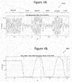
- Figure 4A illustrates a graph 400A of an output of a resampler 216 of the demodulator 200 of Figure 2 .
- the graph 400A is amplitude versus samples.
- the carrier signal starts unmodulated, is then modulated, and then unmodulated, etc.
- the initial unmodulated portion is prior to the reader and target establishing a communication session, and thus is in steady state.
- the second unmodulated portion is higher than the first unmodulated portion due to a transient overshoot. If the communication system has enough time to settle down after modulation, the system will eventually return back to steady state.
- the unmodulated carrier signal is shown in the graph 400A as varying between approximately +1500 and -1500, for a total range of approximately 3000 sampling on the positive and negative peaks.
- the modulated amplitude peak is about 25% of the unmodulated amplitude peak, varying between approximately +250 and -250.
- Figure 4B illustrates the demodulator output signal of the carrier signal in graph 400A.
- the graph 400B is amplitude versus samples.
- the unmodulated amplitude is about 3000.
- the modulated amplitude is about -500.
- the phase change in modulated carrier causes the signs of the samples flip.
- the difference in amplitude between the unmodulated and modulated samples is increased artificially.
- Figure 5 is a flowchart 500 illustrating an example of a method of decoding in accordance with an aspect of the disclosure.
- the peak sampler 110/210 controls the ADC 112/212 or digital resampler 216 to sample a carrier signal in an unmodulated state at peaks.
- the peak sampler 110/210 controls the ADC 112/212 or digital resampler 216 to sample the carrier signal in a modulated state at a sampling phase of the unmodulated state.
- the envelope builder 120 determines an envelope signal based on differentials between maximum and minimum peaks of respective cycles of the sampled carrier signal.
- the demodulators 100, 200 leverage on the phase shift caused by the inherent properties of load modulation. There will be a performance improvement. However, the improvement will vary with the loads, antennas and distance between the NFC target and reader. Also, implementation cost is lower.
- the present disclosure is also directed to a noncoherent demodulator configured to demodulate the phase and amplitude of a load modulated signal.
- the demodulator of this disclosure separates the load modulated signal from the unmodulated carrier signal, and the demodulator outputs an absolute value of the load modulated signal. Since both amplitude and phase of the dynamics of the load modulated contributes to the demodulator output, the bit detector coupled with the demodulator has better sensitivity even when the amplitude of load modulation is below the receiver's amplitude sensitivity.
- Figure 6 illustrates a schematic diagram of a demodulator 600 in accordance with an aspect of the disclosure.
- the demodulator 600 comprises an analog-to-digital converter (ADC) 610, a pair of mixers 620, a pair of low-pass filters (LPF) 630, an offset estimator 640, a load modulated signal estimator 650, and an envelope builder 660.
- ADC analog-to-digital converter
- LPF low-pass filters
- the ADC 610 is configured to sample a carrier signal at a sampling frequency Fs.
- the sampling frequency Fs is greater than twice the carrier frequency (2*Fc) to satisfy the Nyquist theorem.
- the mixer 620 is coupled to the output of the ADC 610, and has two paths to determine the in-phase and quadrature components of the sampled carrier signal.
- the mixer frequency in this example is the carrier frequency Fc.
- the mixer 620 comprises an in-phase component mixer 620I configured to mix the samples of the carrier signal with a cosine function, and a quadrature component mixer 620Q configured to mix the samples of the carrier signal with a sine function.
- the LPF 630 is coupled to the output of the mixer 620, and is configured to filter out frequency components greater than a predetermined frequency (e.g. 2*Fc) from the mixed in-phase and quadrature components of the carrier signal and output the in-phase component signal I and the quadrature component signal Q.
- the LPF 630 comprises an in-phase component low-pass filter 630I configured to filter out frequency components from the mixed in-phase component of the carrier signal, and a quadrature component low-pass filter 630Q configured to filter out frequency components from the mixed quadrature component of the carrier signal.
- the offset estimator 640 is coupled to the output of the LPF 630, and is configured to estimate in-phase and quadrature components of the carrier signal when the carrier signal is in an unmodulated state to determine in-phase and quadrature component offsets.
- the offset estimator 640 comprises an in-phase offset estimator 640I configured to estimate the in-phase component offset Ic of the carrier signal in the unmodulated state by averaging in-phase component samples of the carrier signal in the unmodulated state.
- the offset estimator 640 also comprises a quadrature offset estimator 640Q configured to estimate the quadrature component offset Qc of the carrier signal in the unmodulated state by averaging quadrature component samples of the carrier signal in the unmodulated state.
- the number of samples of the carrier signal averaged by each of the in-phase offset estimator 640I and the quadrature offset estimator 640Q may be, for example, 256 samples.
- Each of the offsets Ic, Qc is a sum of samples divided by the number of samples. Averages of the carrier signal samples are used as offsets so as to reduce noise impact. If the signal-to-noise ratio is high, for example, higher than 40dB, no averaging is needed.
- the offset may be a moving average or a mean of a number of samples.
- the offset estimator 640 is configured to estimate the in-phase and quadrature components Ic, Qc of the carrier signal in the unmodulated state for a predetermined period of time following the wireless communication reader establishing a communication session with a wireless tag. When the reader and tag start communicating, it will take some time before the tag starts to modulate the carrier signal. At the beginning of the communication session the in-phase and quadrature component offsets Ic, Qc are determined, then these offsets are fixed for the modulated state.
- the mode when the offset estimator 630 updates the in-phase and quadrature component offsets may be controlled by firmware when the timing of the unmodulated signal state is known.
- the load modulated signal estimator 650 is configured to estimate in-phase and quadrature components X, Y of a load modulated signal by removing the in-phase and quadrature component offsets Ic, Qc from in-phase and quadrature component samples I, Q of the carrier signal.
- the load modulated signal estimator 650 comprises an in-phase component load modulated signal 650I and a quadrature component load modulated signal estimator 650Q.
- the in-phase component load modulated signal estimator 650I has a positive input coupled to an output of the in-phase component LPF 630I and a negative input coupled to an output of the in-phase offset estimator 640I.
- the in-phase component load modulated signal estimator 650I is configured to remove the in-phase component offset Ic of the carrier signal in the unmodulated state from the in-phase component samples I of the carrier signal.
- the quadrature component load modulated signal estimator 650Q has a positive input coupled to an output of the quadrature component LPF 630Q and a negative input coupled to the output of the quadrature offset estimator 640Q.
- the quadrature component load modulated signal estimator 650Q is configured to remove the quadrature component offset Qc of the carrier signal in the unmodulated state from the quadrature component samples Q of the carrier signal.
- the envelope builder 660 is coupled to the output of the load modulated signal estimator 650, and is configured to build an envelope signal Z by combining X and Y signals.
- Z may be the sum of the square of X and the square of Y.
- Z is the sum of absolute values of the in-phase X and quadrature component Y outputs of the load modulated signal.
- is the absolute value of the quadrature component of the load modulated signal.
- Equation 8 is easier and less expensive to implement.
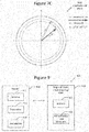
- Figures 7A-7C illustrate in-phase and quadrature plots 700 of the demodulator 600 of Figure 6 .
- Modulation information may be obtained by looking for a difference between the unmodulated carrier signal and the modulated carrier signal, and the difference could be in amplitude, phase, or both. There is no need for a decision mechanism for looking at the amplitude separately, phase separately, and then determine which is used.
- Each of the plots 700 illustrates an unmodulated carrier signal (I,Q) with a thin line, a modulated carrier signal (I',Q') with a bold line, and a load modulated signal representing the difference between the unmodulated and modulated carrier signals with a dashed line.
- Figure 7A illustrates a plot 700A of a difference in carrier signal phase only (i.e., pure PSK modulation), such as in the communication hole discussed above.
- Figure 7B illustrates a plot 700B of a difference in carrier signal amplitude only (i.e., pure ASK modulation).
- Figure 7C illustrates a plot 700C of a difference in both carrier signal amplitude and phase.
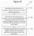
- Figure 8 is a flowchart 800 of a method of decoding in accordance with an aspect of the disclosure.
- the offset estimator estimates in-phase and quadrature component offsets Ic, Qc of a carrier signal in an unmodulated state.
- the load modulated signal estimator 650 estimates in-phase and quadrature components X, Y of a load modulated signal by removing the in-phase and quadrature component offsets Ic, Qc from in-phase and quadrature component samples I, Q of the carrier signal.
- the envelope builder 660 builds an envelope signal by combining absolute values of the in-phase and quadrature components X, Y of the load modulated signal.
- the demodulator 600 is advantageous over prior demodulators in that phase information is included more simply in the input samples to the bit detector, while the demodulator 600 remains low in cost.
- the demodulator 600 also demodulates carrier signals with small or zero amplitude load modulation indices, that is, during communication holes.
- the demodulator 600 also reduces a dynamic range needed for the bit detector. Since the demodulator uses a difference between the unmodulated and modulated carrier signals, and the phase difference is typically below ⁇ /4, the demodulator 600 is not processing absolute signal values, and thus there can be a much lower dynamic range as compared with previous demodulators.
- Figure 9 illustrates a schematic diagram of a wireless system 900.
- the wireless communication system 900 is a Near Field Communication (NFC) system, though the disclosure is not limited in this respect.
- the wireless communication system 900 may be any short range (e.g., a few centimeters) communication (e.g., NFC) involving antenna coupling.
- the wireless communication system 900 comprises a reader 910 and a target or device emulating a tag/card 920.
- the reader 910 comprises an antenna 912, a transmitter 914, and a demodulator 916, as well as other well-known components.
- the demodulator 914 is one of the demodulators described above with respect to Figures 1 , 2 , and 6 .
- the target or device emulating a tag/card 920 comprises an antenna 922 and an active/passive load modulator 926, along with other well-known components, and is configured to communicate with the reader 910 by modulating the carrier signal with data.
- the data may be modulated on the carrier signal using Amplitude Shift Keying (ASK) by switching the load impedances, though the disclosure is not limited in this respect.
- ASK Amplitude Shift Keying
- the tag or device emulating a tag/card 920 may use any modulating technique as suitable for the intended purpose.
Landscapes
- Engineering & Computer Science (AREA)
- Computer Networks & Wireless Communication (AREA)
- Signal Processing (AREA)
- Power Engineering (AREA)
- Health & Medical Sciences (AREA)
- Toxicology (AREA)
- Physics & Mathematics (AREA)
- Electromagnetism (AREA)
- General Health & Medical Sciences (AREA)
- Artificial Intelligence (AREA)
- Computer Vision & Pattern Recognition (AREA)
- General Physics & Mathematics (AREA)
- Theoretical Computer Science (AREA)
- Digital Transmission Methods That Use Modulated Carrier Waves (AREA)
- Near-Field Transmission Systems (AREA)
Applications Claiming Priority (1)
| Application Number | Priority Date | Filing Date | Title |
|---|---|---|---|
| US15/088,636 US10148322B2 (en) | 2016-04-01 | 2016-04-01 | Demodulator of a wireless communication reader |
Publications (3)
| Publication Number | Publication Date |
|---|---|
| EP3226433A2 true EP3226433A2 (de) | 2017-10-04 |
| EP3226433A3 EP3226433A3 (de) | 2017-10-25 |
| EP3226433B1 EP3226433B1 (de) | 2019-03-27 |
Family
ID=58231410
Family Applications (1)
| Application Number | Title | Priority Date | Filing Date |
|---|---|---|---|
| EP17158554.0A Active EP3226433B1 (de) | 2016-04-01 | 2017-02-28 | Demodulator eines drahtloskommunikationslesers |
Country Status (3)
| Country | Link |
|---|---|
| US (1) | US10148322B2 (de) |
| EP (1) | EP3226433B1 (de) |
| CN (1) | CN107276939B (de) |
Families Citing this family (12)
| Publication number | Priority date | Publication date | Assignee | Title |
|---|---|---|---|---|
| SG10201509261UA (en) * | 2015-11-09 | 2017-06-29 | Huawei Int Pte Ltd | Apparatus and method for direct radio frequency (rf) sampling in near field communication (nfc) devices |
| CN110557118B (zh) * | 2018-05-31 | 2022-12-27 | 华为技术有限公司 | 一种锁相装置及锁相方法 |
| US10785015B1 (en) * | 2019-04-30 | 2020-09-22 | Keyssa Systems, Inc. | Multiple phase symbol synchronization for amplifier sampler accepting modulated signal |
| EP3736994B1 (de) * | 2019-05-09 | 2023-05-03 | Nxp B.V. | Genaue detektion des endes einer pause-a für nahfeldkommunikationen |
| US10771187B1 (en) * | 2019-10-18 | 2020-09-08 | Arm Limited | Adaptive coding for wireless communication |
| KR102925429B1 (ko) * | 2019-11-12 | 2026-02-11 | 삼성전자주식회사 | 무선 통신 장치 및 방법 |
| US11366779B2 (en) | 2019-11-15 | 2022-06-21 | Arm Limited | System-in-package architecture with wireless bus interconnect |
| KR102690677B1 (ko) | 2019-11-25 | 2024-08-01 | 삼성전자주식회사 | 근거리 통신 장치 및 근거리 통신 장치의 동작 방법 |
| CN111800170A (zh) * | 2020-06-24 | 2020-10-20 | 易兆微电子(杭州)股份有限公司 | 一种用于负载调制的峰值检测方法 |
| CN113055326B (zh) * | 2021-03-10 | 2022-06-17 | 四川省博瑞恩科技有限公司 | 一种基于采样相减方法的幅移键控解调电路 |
| US11985014B2 (en) * | 2022-06-03 | 2024-05-14 | Renesas Electronics America Inc. | Digital demodulation for wireless power |
| KR20240132897A (ko) | 2023-02-27 | 2024-09-04 | 삼성전자주식회사 | Nfc 장치의 동작 방법 및 이를 수행하는 nfc 장치 |
Family Cites Families (22)
| Publication number | Priority date | Publication date | Assignee | Title |
|---|---|---|---|---|
| US4864167A (en) * | 1988-08-01 | 1989-09-05 | Tektronix, Inc. | Dual function peak metering circuit |
| US4887050A (en) | 1989-03-31 | 1989-12-12 | Motorola, Inc. | Frequency control apparatus and method for a digital radio receiver |
| US6757340B1 (en) | 1999-02-22 | 2004-06-29 | Telefonaktiebolaget L M Ericsson (Publ) | Radio receiver and method for preloading an average DC-offset into a channel filter |
| US7010073B2 (en) * | 2001-01-19 | 2006-03-07 | Qualcomm, Incorporated | Delay lock loops for wireless communication systems |
| US6700514B2 (en) | 2002-03-14 | 2004-03-02 | Nec Corporation | Feed-forward DC-offset canceller for direct conversion receiver |
| US8559559B2 (en) | 2002-06-20 | 2013-10-15 | Qualcomm, Incorporated | Method and apparatus for compensating DC offsets in communication systems |
| JP4030482B2 (ja) | 2003-08-18 | 2008-01-09 | シャープ株式会社 | I/q復調回路 |
| WO2006009871A1 (en) * | 2004-06-17 | 2006-01-26 | W5 Networks, Inc. | Low power wireless communication system and protocol |
| GB0501593D0 (en) | 2005-01-25 | 2005-03-02 | Innovision Res & Tech Plc | Demodulation apparatus and method |
| US20070026825A1 (en) * | 2005-02-24 | 2007-02-01 | Innovision Research & Technology Plc | NFC device and apparatus |
| JP2006252681A (ja) * | 2005-03-11 | 2006-09-21 | Hitachi Ltd | 光ディスク装置及びpll回路 |
| GB2437574B (en) | 2006-04-28 | 2008-06-25 | Motorola Inc | Receiver for use in wireless communications and method of operation of the receiver |
| WO2008093254A1 (en) | 2007-01-31 | 2008-08-07 | Nxp B.V. | Demodulation circuit for ask coded or amplitude modulated signals as well as nfc and rfid devices comprising the same |
| US8175192B2 (en) * | 2007-04-02 | 2012-05-08 | Broadcom Corporation | Method and system for determining and removing DC offset in communication signals |
| TWI401923B (zh) * | 2009-06-06 | 2013-07-11 | Generalplus Technology Inc | 適應性時脈重建方法與裝置以及進行音頻解碼方法 |
| US8427974B2 (en) * | 2009-10-22 | 2013-04-23 | Jds Uniphase Corporation | Identifying an origin of a DOCSIS upstream burst |
| US8605816B2 (en) * | 2010-05-27 | 2013-12-10 | Sony Corporation | Non-contact wireless communication apparatus, method of waveform-shaping envelope curve, and mobile electronic device |
| US8867990B2 (en) * | 2012-02-29 | 2014-10-21 | Broadcom Corporation | Detecting a presence of near field communications (NFC) devices |
| EP2940916B1 (de) * | 2014-05-02 | 2017-03-22 | Nxp B.V. | Symboltaktrückgewinnungsschaltung |
| CN104362981A (zh) * | 2014-08-27 | 2015-02-18 | 北京中电华大电子设计有限责任公司 | 一种同步采样解调方法和电路 |
| JP6341105B2 (ja) * | 2015-01-26 | 2018-06-13 | 株式会社Jvcケンウッド | Fm受信装置、fm受信方法 |
| CN105337915B (zh) * | 2015-09-30 | 2018-09-18 | 电信科学技术第一研究所有限公司 | π/4-QPSK解调器基带采样数据最佳采样点的获取方法 |
-
2016
- 2016-04-01 US US15/088,636 patent/US10148322B2/en not_active Expired - Fee Related
-
2017
- 2017-02-28 EP EP17158554.0A patent/EP3226433B1/de active Active
- 2017-03-02 CN CN201710121731.5A patent/CN107276939B/zh not_active Expired - Fee Related
Non-Patent Citations (1)
| Title |
|---|
| None |
Also Published As
| Publication number | Publication date |
|---|---|
| US10148322B2 (en) | 2018-12-04 |
| CN107276939B (zh) | 2020-09-18 |
| US20170288741A1 (en) | 2017-10-05 |
| EP3226433A3 (de) | 2017-10-25 |
| CN107276939A (zh) | 2017-10-20 |
| EP3226433B1 (de) | 2019-03-27 |
Similar Documents
| Publication | Publication Date | Title |
|---|---|---|
| EP3226433B1 (de) | Demodulator eines drahtloskommunikationslesers | |
| CN102934378B (zh) | 频率偏移估计装置、接收装置、频率偏移估计方法及接收方法 | |
| US4896336A (en) | Differential phase-shift keying demodulator | |
| KR100379723B1 (ko) | 디지탈적으로보상된직접변환수신기 | |
| US9712317B2 (en) | Carrier synchronization appropriate for ALM NFC data transmission | |
| CN108141251B (zh) | Nfc卡仿真模式的异步传输 | |
| CN107079233B (zh) | 用于近场通信(nfc)设备中的直接射频(rf)采样的装置和方法 | |
| US8463121B2 (en) | Ultra wide-range frequency offset estimation for digital coherent optical receivers | |
| WO2001020863A9 (en) | Method and apparatus for carrier phase tracking | |
| US20050008101A1 (en) | Computationally efficient demodulation for differential phase shift keying | |
| US10491437B2 (en) | Circuits for amplitude demodulation and related methods | |
| US8792846B2 (en) | Demodulator and method for demodulating a modulated carrier signal | |
| EP0924892A2 (de) | Schaltung zur Rückgewinnung des Bittaktes und Verfahren zur Rückgewinnung des Bittaktes | |
| EP1213890A2 (de) | Phasennachlauf vierter Ordnung für DPSK-Empfänger | |
| KR20240010366A (ko) | 반송파 주파수 오류 추정 방법 및 장치 | |
| US8519825B2 (en) | RFID transponder | |
| US20070189420A1 (en) | Limiter based analog demodulator | |
| US7746958B2 (en) | Receiver for a wire-free communication system | |
| US8472909B2 (en) | Filter device for detecting and/or removing erroneous components in and/or from a signal | |
| KR101000230B1 (ko) | 차동 이진 위상 편이 변조 방식을 이용한 무선 식별 시스템및 방법 | |
| CN121418238A (zh) | 基于rpa-dtft载波估计与ask定时的同步方法及系统 | |
| JPH07212423A (ja) | データ受信装置 | |
| US20040247064A1 (en) | Differential detector | |
| CN113726706A (zh) | 一种提高d8psk信号解调精度的方法、装置及存储介质 | |
| JPH0630072A (ja) | 直交振幅変調波の搬送波再生回路 |
Legal Events
| Date | Code | Title | Description |
|---|---|---|---|
| PUAI | Public reference made under article 153(3) epc to a published international application that has entered the european phase |
Free format text: ORIGINAL CODE: 0009012 |
|
| STAA | Information on the status of an ep patent application or granted ep patent |
Free format text: STATUS: REQUEST FOR EXAMINATION WAS MADE |
|
| PUAL | Search report despatched |
Free format text: ORIGINAL CODE: 0009013 |
|
| 17P | Request for examination filed |
Effective date: 20170228 |
|
| AK | Designated contracting states |
Kind code of ref document: A2 Designated state(s): AL AT BE BG CH CY CZ DE DK EE ES FI FR GB GR HR HU IE IS IT LI LT LU LV MC MK MT NL NO PL PT RO RS SE SI SK SM TR |
|
| AX | Request for extension of the european patent |
Extension state: BA ME |
|
| AK | Designated contracting states |
Kind code of ref document: A3 Designated state(s): AL AT BE BG CH CY CZ DE DK EE ES FI FR GB GR HR HU IE IS IT LI LT LU LV MC MK MT NL NO PL PT RO RS SE SI SK SM TR |
|
| AX | Request for extension of the european patent |
Extension state: BA ME |
|
| RIC1 | Information provided on ipc code assigned before grant |
Ipc: H03D 1/00 20060101ALI20170915BHEP Ipc: H03D 3/06 20060101ALN20170915BHEP Ipc: H03D 1/02 20060101ALI20170915BHEP Ipc: H04W 4/00 20090101ALI20170915BHEP Ipc: H04L 27/233 20060101ALN20170915BHEP Ipc: H03D 1/22 20060101ALI20170915BHEP Ipc: H04L 27/06 20060101ALN20170915BHEP Ipc: H04B 5/00 20060101AFI20170915BHEP Ipc: H04L 25/06 20060101ALI20170915BHEP Ipc: H03D 3/18 20060101ALN20170915BHEP Ipc: H03D 3/00 20060101ALN20170915BHEP Ipc: H03K 9/02 20060101ALN20170915BHEP |
|
| REG | Reference to a national code |
Ref country code: DE Ref legal event code: R079 Ref document number: 602017002877 Country of ref document: DE Free format text: PREVIOUS MAIN CLASS: H04B0005000000 Ipc: H04B0005020000 |
|
| GRAP | Despatch of communication of intention to grant a patent |
Free format text: ORIGINAL CODE: EPIDOSNIGR1 |
|
| STAA | Information on the status of an ep patent application or granted ep patent |
Free format text: STATUS: GRANT OF PATENT IS INTENDED |
|
| RIC1 | Information provided on ipc code assigned before grant |
Ipc: H04W 4/80 20180101ALI20180904BHEP Ipc: H04B 5/02 20060101AFI20180904BHEP Ipc: H04L 27/06 20060101ALI20180904BHEP Ipc: H03D 1/22 20060101ALI20180904BHEP Ipc: H04B 5/00 20060101ALI20180904BHEP Ipc: H04L 27/233 20060101ALI20180904BHEP Ipc: H04L 25/06 20060101ALI20180904BHEP |
|
| INTG | Intention to grant announced |
Effective date: 20181004 |
|
| GRAS | Grant fee paid |
Free format text: ORIGINAL CODE: EPIDOSNIGR3 |
|
| GRAA | (expected) grant |
Free format text: ORIGINAL CODE: 0009210 |
|
| STAA | Information on the status of an ep patent application or granted ep patent |
Free format text: STATUS: THE PATENT HAS BEEN GRANTED |
|
| AK | Designated contracting states |
Kind code of ref document: B1 Designated state(s): AL AT BE BG CH CY CZ DE DK EE ES FI FR GB GR HR HU IE IS IT LI LT LU LV MC MK MT NL NO PL PT RO RS SE SI SK SM TR |
|
| REG | Reference to a national code |
Ref country code: GB Ref legal event code: FG4D |
|
| REG | Reference to a national code |
Ref country code: CH Ref legal event code: EP |
|
| REG | Reference to a national code |
Ref country code: AT Ref legal event code: REF Ref document number: 1114251 Country of ref document: AT Kind code of ref document: T Effective date: 20190415 |
|
| REG | Reference to a national code |
Ref country code: IE Ref legal event code: FG4D |
|
| REG | Reference to a national code |
Ref country code: DE Ref legal event code: R096 Ref document number: 602017002877 Country of ref document: DE |
|
| REG | Reference to a national code |
Ref country code: NL Ref legal event code: FP |
|
| PG25 | Lapsed in a contracting state [announced via postgrant information from national office to epo] |
Ref country code: LT Free format text: LAPSE BECAUSE OF FAILURE TO SUBMIT A TRANSLATION OF THE DESCRIPTION OR TO PAY THE FEE WITHIN THE PRESCRIBED TIME-LIMIT Effective date: 20190327 Ref country code: SE Free format text: LAPSE BECAUSE OF FAILURE TO SUBMIT A TRANSLATION OF THE DESCRIPTION OR TO PAY THE FEE WITHIN THE PRESCRIBED TIME-LIMIT Effective date: 20190327 Ref country code: NO Free format text: LAPSE BECAUSE OF FAILURE TO SUBMIT A TRANSLATION OF THE DESCRIPTION OR TO PAY THE FEE WITHIN THE PRESCRIBED TIME-LIMIT Effective date: 20190627 Ref country code: FI Free format text: LAPSE BECAUSE OF FAILURE TO SUBMIT A TRANSLATION OF THE DESCRIPTION OR TO PAY THE FEE WITHIN THE PRESCRIBED TIME-LIMIT Effective date: 20190327 |
|
| PG25 | Lapsed in a contracting state [announced via postgrant information from national office to epo] |
Ref country code: HR Free format text: LAPSE BECAUSE OF FAILURE TO SUBMIT A TRANSLATION OF THE DESCRIPTION OR TO PAY THE FEE WITHIN THE PRESCRIBED TIME-LIMIT Effective date: 20190327 Ref country code: LV Free format text: LAPSE BECAUSE OF FAILURE TO SUBMIT A TRANSLATION OF THE DESCRIPTION OR TO PAY THE FEE WITHIN THE PRESCRIBED TIME-LIMIT Effective date: 20190327 Ref country code: BG Free format text: LAPSE BECAUSE OF FAILURE TO SUBMIT A TRANSLATION OF THE DESCRIPTION OR TO PAY THE FEE WITHIN THE PRESCRIBED TIME-LIMIT Effective date: 20190627 Ref country code: RS Free format text: LAPSE BECAUSE OF FAILURE TO SUBMIT A TRANSLATION OF THE DESCRIPTION OR TO PAY THE FEE WITHIN THE PRESCRIBED TIME-LIMIT Effective date: 20190327 Ref country code: GR Free format text: LAPSE BECAUSE OF FAILURE TO SUBMIT A TRANSLATION OF THE DESCRIPTION OR TO PAY THE FEE WITHIN THE PRESCRIBED TIME-LIMIT Effective date: 20190628 |
|
| REG | Reference to a national code |
Ref country code: AT Ref legal event code: MK05 Ref document number: 1114251 Country of ref document: AT Kind code of ref document: T Effective date: 20190327 |
|
| PG25 | Lapsed in a contracting state [announced via postgrant information from national office to epo] |
Ref country code: EE Free format text: LAPSE BECAUSE OF FAILURE TO SUBMIT A TRANSLATION OF THE DESCRIPTION OR TO PAY THE FEE WITHIN THE PRESCRIBED TIME-LIMIT Effective date: 20190327 Ref country code: SK Free format text: LAPSE BECAUSE OF FAILURE TO SUBMIT A TRANSLATION OF THE DESCRIPTION OR TO PAY THE FEE WITHIN THE PRESCRIBED TIME-LIMIT Effective date: 20190327 Ref country code: PT Free format text: LAPSE BECAUSE OF FAILURE TO SUBMIT A TRANSLATION OF THE DESCRIPTION OR TO PAY THE FEE WITHIN THE PRESCRIBED TIME-LIMIT Effective date: 20190727 Ref country code: AL Free format text: LAPSE BECAUSE OF FAILURE TO SUBMIT A TRANSLATION OF THE DESCRIPTION OR TO PAY THE FEE WITHIN THE PRESCRIBED TIME-LIMIT Effective date: 20190327 Ref country code: CZ Free format text: LAPSE BECAUSE OF FAILURE TO SUBMIT A TRANSLATION OF THE DESCRIPTION OR TO PAY THE FEE WITHIN THE PRESCRIBED TIME-LIMIT Effective date: 20190327 Ref country code: ES Free format text: LAPSE BECAUSE OF FAILURE TO SUBMIT A TRANSLATION OF THE DESCRIPTION OR TO PAY THE FEE WITHIN THE PRESCRIBED TIME-LIMIT Effective date: 20190327 Ref country code: IT Free format text: LAPSE BECAUSE OF FAILURE TO SUBMIT A TRANSLATION OF THE DESCRIPTION OR TO PAY THE FEE WITHIN THE PRESCRIBED TIME-LIMIT Effective date: 20190327 Ref country code: RO Free format text: LAPSE BECAUSE OF FAILURE TO SUBMIT A TRANSLATION OF THE DESCRIPTION OR TO PAY THE FEE WITHIN THE PRESCRIBED TIME-LIMIT Effective date: 20190327 |
|
| PG25 | Lapsed in a contracting state [announced via postgrant information from national office to epo] |
Ref country code: SM Free format text: LAPSE BECAUSE OF FAILURE TO SUBMIT A TRANSLATION OF THE DESCRIPTION OR TO PAY THE FEE WITHIN THE PRESCRIBED TIME-LIMIT Effective date: 20190327 Ref country code: PL Free format text: LAPSE BECAUSE OF FAILURE TO SUBMIT A TRANSLATION OF THE DESCRIPTION OR TO PAY THE FEE WITHIN THE PRESCRIBED TIME-LIMIT Effective date: 20190327 |
|
| PG25 | Lapsed in a contracting state [announced via postgrant information from national office to epo] |
Ref country code: AT Free format text: LAPSE BECAUSE OF FAILURE TO SUBMIT A TRANSLATION OF THE DESCRIPTION OR TO PAY THE FEE WITHIN THE PRESCRIBED TIME-LIMIT Effective date: 20190327 Ref country code: IS Free format text: LAPSE BECAUSE OF FAILURE TO SUBMIT A TRANSLATION OF THE DESCRIPTION OR TO PAY THE FEE WITHIN THE PRESCRIBED TIME-LIMIT Effective date: 20190727 |
|
| REG | Reference to a national code |
Ref country code: DE Ref legal event code: R097 Ref document number: 602017002877 Country of ref document: DE |
|
| PG25 | Lapsed in a contracting state [announced via postgrant information from national office to epo] |
Ref country code: DK Free format text: LAPSE BECAUSE OF FAILURE TO SUBMIT A TRANSLATION OF THE DESCRIPTION OR TO PAY THE FEE WITHIN THE PRESCRIBED TIME-LIMIT Effective date: 20190327 |
|
| PLBE | No opposition filed within time limit |
Free format text: ORIGINAL CODE: 0009261 |
|
| STAA | Information on the status of an ep patent application or granted ep patent |
Free format text: STATUS: NO OPPOSITION FILED WITHIN TIME LIMIT |
|
| PG25 | Lapsed in a contracting state [announced via postgrant information from national office to epo] |
Ref country code: SI Free format text: LAPSE BECAUSE OF FAILURE TO SUBMIT A TRANSLATION OF THE DESCRIPTION OR TO PAY THE FEE WITHIN THE PRESCRIBED TIME-LIMIT Effective date: 20190327 |
|
| 26N | No opposition filed |
Effective date: 20200103 |
|
| PG25 | Lapsed in a contracting state [announced via postgrant information from national office to epo] |
Ref country code: TR Free format text: LAPSE BECAUSE OF FAILURE TO SUBMIT A TRANSLATION OF THE DESCRIPTION OR TO PAY THE FEE WITHIN THE PRESCRIBED TIME-LIMIT Effective date: 20190327 |
|
| REG | Reference to a national code |
Ref country code: DE Ref legal event code: R119 Ref document number: 602017002877 Country of ref document: DE |
|
| REG | Reference to a national code |
Ref country code: CH Ref legal event code: PL |
|
| REG | Reference to a national code |
Ref country code: NL Ref legal event code: MM Effective date: 20200301 |
|
| REG | Reference to a national code |
Ref country code: BE Ref legal event code: MM Effective date: 20200229 |
|
| PG25 | Lapsed in a contracting state [announced via postgrant information from national office to epo] |
Ref country code: LU Free format text: LAPSE BECAUSE OF NON-PAYMENT OF DUE FEES Effective date: 20200228 Ref country code: MC Free format text: LAPSE BECAUSE OF FAILURE TO SUBMIT A TRANSLATION OF THE DESCRIPTION OR TO PAY THE FEE WITHIN THE PRESCRIBED TIME-LIMIT Effective date: 20190327 |
|
| PG25 | Lapsed in a contracting state [announced via postgrant information from national office to epo] |
Ref country code: LI Free format text: LAPSE BECAUSE OF NON-PAYMENT OF DUE FEES Effective date: 20200229 Ref country code: CH Free format text: LAPSE BECAUSE OF NON-PAYMENT OF DUE FEES Effective date: 20200229 |
|
| PG25 | Lapsed in a contracting state [announced via postgrant information from national office to epo] |
Ref country code: NL Free format text: LAPSE BECAUSE OF NON-PAYMENT OF DUE FEES Effective date: 20200301 |
|
| PG25 | Lapsed in a contracting state [announced via postgrant information from national office to epo] |
Ref country code: FR Free format text: LAPSE BECAUSE OF NON-PAYMENT OF DUE FEES Effective date: 20200229 Ref country code: IE Free format text: LAPSE BECAUSE OF NON-PAYMENT OF DUE FEES Effective date: 20200228 Ref country code: DE Free format text: LAPSE BECAUSE OF NON-PAYMENT OF DUE FEES Effective date: 20200901 |
|
| PG25 | Lapsed in a contracting state [announced via postgrant information from national office to epo] |
Ref country code: BE Free format text: LAPSE BECAUSE OF NON-PAYMENT OF DUE FEES Effective date: 20200229 |
|
| GBPC | Gb: european patent ceased through non-payment of renewal fee |
Effective date: 20210228 |
|
| PG25 | Lapsed in a contracting state [announced via postgrant information from national office to epo] |
Ref country code: GB Free format text: LAPSE BECAUSE OF NON-PAYMENT OF DUE FEES Effective date: 20210228 |
|
| PG25 | Lapsed in a contracting state [announced via postgrant information from national office to epo] |
Ref country code: MT Free format text: LAPSE BECAUSE OF FAILURE TO SUBMIT A TRANSLATION OF THE DESCRIPTION OR TO PAY THE FEE WITHIN THE PRESCRIBED TIME-LIMIT Effective date: 20190327 Ref country code: CY Free format text: LAPSE BECAUSE OF FAILURE TO SUBMIT A TRANSLATION OF THE DESCRIPTION OR TO PAY THE FEE WITHIN THE PRESCRIBED TIME-LIMIT Effective date: 20190327 |
|
| PG25 | Lapsed in a contracting state [announced via postgrant information from national office to epo] |
Ref country code: MK Free format text: LAPSE BECAUSE OF FAILURE TO SUBMIT A TRANSLATION OF THE DESCRIPTION OR TO PAY THE FEE WITHIN THE PRESCRIBED TIME-LIMIT Effective date: 20190327 |