EP3226302A1 - Method for fabricating finfet structure - Google Patents
Method for fabricating finfet structure Download PDFInfo
- Publication number
- EP3226302A1 EP3226302A1 EP17162505.6A EP17162505A EP3226302A1 EP 3226302 A1 EP3226302 A1 EP 3226302A1 EP 17162505 A EP17162505 A EP 17162505A EP 3226302 A1 EP3226302 A1 EP 3226302A1
- Authority
- EP
- European Patent Office
- Prior art keywords
- layer
- fin structure
- semiconductor
- recesses
- semiconductor substrate
- Prior art date
- Legal status (The legal status is an assumption and is not a legal conclusion. Google has not performed a legal analysis and makes no representation as to the accuracy of the status listed.)
- Withdrawn
Links
Images




Classifications
-
- H—ELECTRICITY
- H10—SEMICONDUCTOR DEVICES; ELECTRIC SOLID-STATE DEVICES NOT OTHERWISE PROVIDED FOR
- H10D—INORGANIC ELECTRIC SEMICONDUCTOR DEVICES
- H10D30/00—Field-effect transistors [FET]
- H10D30/60—Insulated-gate field-effect transistors [IGFET]
- H10D30/62—Fin field-effect transistors [FinFET]
-
- H—ELECTRICITY
- H10—SEMICONDUCTOR DEVICES; ELECTRIC SOLID-STATE DEVICES NOT OTHERWISE PROVIDED FOR
- H10D—INORGANIC ELECTRIC SEMICONDUCTOR DEVICES
- H10D30/00—Field-effect transistors [FET]
- H10D30/01—Manufacture or treatment
- H10D30/021—Manufacture or treatment of FETs having insulated gates [IGFET]
- H10D30/024—Manufacture or treatment of FETs having insulated gates [IGFET] of fin field-effect transistors [FinFET]
-
- H—ELECTRICITY
- H10—SEMICONDUCTOR DEVICES; ELECTRIC SOLID-STATE DEVICES NOT OTHERWISE PROVIDED FOR
- H10D—INORGANIC ELECTRIC SEMICONDUCTOR DEVICES
- H10D62/00—Semiconductor bodies, or regions thereof, of devices having potential barriers
- H10D62/10—Shapes, relative sizes or dispositions of the regions of the semiconductor bodies; Shapes of the semiconductor bodies
- H10D62/113—Isolations within a component, i.e. internal isolations
- H10D62/115—Dielectric isolations, e.g. air gaps
-
- H—ELECTRICITY
- H10—SEMICONDUCTOR DEVICES; ELECTRIC SOLID-STATE DEVICES NOT OTHERWISE PROVIDED FOR
- H10D—INORGANIC ELECTRIC SEMICONDUCTOR DEVICES
- H10D64/00—Electrodes of devices having potential barriers
- H10D64/01—Manufacture or treatment
- H10D64/015—Manufacture or treatment removing at least parts of gate spacers, e.g. disposable spacers
-
- H—ELECTRICITY
- H10—SEMICONDUCTOR DEVICES; ELECTRIC SOLID-STATE DEVICES NOT OTHERWISE PROVIDED FOR
- H10D—INORGANIC ELECTRIC SEMICONDUCTOR DEVICES
- H10D84/00—Integrated devices formed in or on semiconductor substrates that comprise only semiconducting layers, e.g. on Si wafers or on GaAs-on-Si wafers
- H10D84/01—Manufacture or treatment
- H10D84/0123—Integrating together multiple components covered by H10D12/00 or H10D30/00, e.g. integrating multiple IGBTs
- H10D84/0126—Integrating together multiple components covered by H10D12/00 or H10D30/00, e.g. integrating multiple IGBTs the components including insulated gates, e.g. IGFETs
- H10D84/0158—Integrating together multiple components covered by H10D12/00 or H10D30/00, e.g. integrating multiple IGBTs the components including insulated gates, e.g. IGFETs the components including FinFETs
-
- H—ELECTRICITY
- H10—SEMICONDUCTOR DEVICES; ELECTRIC SOLID-STATE DEVICES NOT OTHERWISE PROVIDED FOR
- H10D—INORGANIC ELECTRIC SEMICONDUCTOR DEVICES
- H10D84/00—Integrated devices formed in or on semiconductor substrates that comprise only semiconducting layers, e.g. on Si wafers or on GaAs-on-Si wafers
- H10D84/01—Manufacture or treatment
- H10D84/02—Manufacture or treatment characterised by using material-based technologies
- H10D84/03—Manufacture or treatment characterised by using material-based technologies using Group IV technology, e.g. silicon technology or silicon-carbide [SiC] technology
- H10D84/038—Manufacture or treatment characterised by using material-based technologies using Group IV technology, e.g. silicon technology or silicon-carbide [SiC] technology using silicon technology, e.g. SiGe
-
- H—ELECTRICITY
- H10—SEMICONDUCTOR DEVICES; ELECTRIC SOLID-STATE DEVICES NOT OTHERWISE PROVIDED FOR
- H10P—GENERIC PROCESSES OR APPARATUS FOR THE MANUFACTURE OR TREATMENT OF DEVICES COVERED BY CLASS H10
- H10P14/00—Formation of materials, e.g. in the shape of layers or pillars
- H10P14/60—Formation of materials, e.g. in the shape of layers or pillars of insulating materials
- H10P14/63—Formation of materials, e.g. in the shape of layers or pillars of insulating materials characterised by the formation processes
- H10P14/6302—Non-deposition formation processes
- H10P14/6304—Formation by oxidation, e.g. oxidation of the substrate
- H10P14/6306—Formation by oxidation, e.g. oxidation of the substrate of the semiconductor materials
- H10P14/6308—Formation by oxidation, e.g. oxidation of the substrate of the semiconductor materials of Group IV semiconductors
-
- H—ELECTRICITY
- H10—SEMICONDUCTOR DEVICES; ELECTRIC SOLID-STATE DEVICES NOT OTHERWISE PROVIDED FOR
- H10P—GENERIC PROCESSES OR APPARATUS FOR THE MANUFACTURE OR TREATMENT OF DEVICES COVERED BY CLASS H10
- H10P14/00—Formation of materials, e.g. in the shape of layers or pillars
- H10P14/60—Formation of materials, e.g. in the shape of layers or pillars of insulating materials
- H10P14/66—Formation of materials, e.g. in the shape of layers or pillars of insulating materials characterised by the type of materials
- H10P14/665—Porous materials
-
- H—ELECTRICITY
- H10—SEMICONDUCTOR DEVICES; ELECTRIC SOLID-STATE DEVICES NOT OTHERWISE PROVIDED FOR
- H10P—GENERIC PROCESSES OR APPARATUS FOR THE MANUFACTURE OR TREATMENT OF DEVICES COVERED BY CLASS H10
- H10P14/00—Formation of materials, e.g. in the shape of layers or pillars
- H10P14/60—Formation of materials, e.g. in the shape of layers or pillars of insulating materials
- H10P14/69—Inorganic materials
- H10P14/692—Inorganic materials composed of oxides, glassy oxides or oxide-based glasses
- H10P14/6921—Inorganic materials composed of oxides, glassy oxides or oxide-based glasses containing silicon
- H10P14/69215—Inorganic materials composed of oxides, glassy oxides or oxide-based glasses containing silicon the material being a silicon oxide, e.g. SiO2
-
- H—ELECTRICITY
- H10—SEMICONDUCTOR DEVICES; ELECTRIC SOLID-STATE DEVICES NOT OTHERWISE PROVIDED FOR
- H10P—GENERIC PROCESSES OR APPARATUS FOR THE MANUFACTURE OR TREATMENT OF DEVICES COVERED BY CLASS H10
- H10P14/00—Formation of materials, e.g. in the shape of layers or pillars
- H10P14/60—Formation of materials, e.g. in the shape of layers or pillars of insulating materials
- H10P14/69—Inorganic materials
- H10P14/692—Inorganic materials composed of oxides, glassy oxides or oxide-based glasses
- H10P14/6921—Inorganic materials composed of oxides, glassy oxides or oxide-based glasses containing silicon
- H10P14/6922—Inorganic materials composed of oxides, glassy oxides or oxide-based glasses containing silicon the material containing Si, O and at least one of H, N, C, F or other non-metal elements, e.g. SiOC, SiOC:H or SiONC
-
- H—ELECTRICITY
- H10—SEMICONDUCTOR DEVICES; ELECTRIC SOLID-STATE DEVICES NOT OTHERWISE PROVIDED FOR
- H10P—GENERIC PROCESSES OR APPARATUS FOR THE MANUFACTURE OR TREATMENT OF DEVICES COVERED BY CLASS H10
- H10P50/00—Etching of wafers, substrates or parts of devices
- H10P50/20—Dry etching; Plasma etching; Reactive-ion etching
- H10P50/28—Dry etching; Plasma etching; Reactive-ion etching of insulating materials
- H10P50/282—Dry etching; Plasma etching; Reactive-ion etching of insulating materials of inorganic materials
- H10P50/283—Dry etching; Plasma etching; Reactive-ion etching of insulating materials of inorganic materials by chemical means
-
- H—ELECTRICITY
- H10—SEMICONDUCTOR DEVICES; ELECTRIC SOLID-STATE DEVICES NOT OTHERWISE PROVIDED FOR
- H10P—GENERIC PROCESSES OR APPARATUS FOR THE MANUFACTURE OR TREATMENT OF DEVICES COVERED BY CLASS H10
- H10P50/00—Etching of wafers, substrates or parts of devices
- H10P50/69—Etching of wafers, substrates or parts of devices using masks for semiconductor materials
- H10P50/691—Etching of wafers, substrates or parts of devices using masks for semiconductor materials for Group V materials or Group III-V materials
- H10P50/692—Etching of wafers, substrates or parts of devices using masks for semiconductor materials for Group V materials or Group III-V materials characterised by their composition, e.g. multilayer masks or materials
-
- H—ELECTRICITY
- H10—SEMICONDUCTOR DEVICES; ELECTRIC SOLID-STATE DEVICES NOT OTHERWISE PROVIDED FOR
- H10W—GENERIC PACKAGES, INTERCONNECTIONS, CONNECTORS OR OTHER CONSTRUCTIONAL DETAILS OF DEVICES COVERED BY CLASS H10
- H10W10/00—Isolation regions in semiconductor bodies between components of integrated devices
- H10W10/01—Manufacture or treatment
- H10W10/011—Manufacture or treatment of isolation regions comprising dielectric materials
- H10W10/012—Manufacture or treatment of isolation regions comprising dielectric materials using local oxidation of silicon [LOCOS]
- H10W10/0121—Manufacture or treatment of isolation regions comprising dielectric materials using local oxidation of silicon [LOCOS] in regions recessed from the surface, e.g. in trenches or grooves
-
- H—ELECTRICITY
- H10—SEMICONDUCTOR DEVICES; ELECTRIC SOLID-STATE DEVICES NOT OTHERWISE PROVIDED FOR
- H10W—GENERIC PACKAGES, INTERCONNECTIONS, CONNECTORS OR OTHER CONSTRUCTIONAL DETAILS OF DEVICES COVERED BY CLASS H10
- H10W10/00—Isolation regions in semiconductor bodies between components of integrated devices
- H10W10/01—Manufacture or treatment
- H10W10/011—Manufacture or treatment of isolation regions comprising dielectric materials
- H10W10/014—Manufacture or treatment of isolation regions comprising dielectric materials using trench refilling with dielectric materials, e.g. shallow trench isolations
-
- H—ELECTRICITY
- H10—SEMICONDUCTOR DEVICES; ELECTRIC SOLID-STATE DEVICES NOT OTHERWISE PROVIDED FOR
- H10W—GENERIC PACKAGES, INTERCONNECTIONS, CONNECTORS OR OTHER CONSTRUCTIONAL DETAILS OF DEVICES COVERED BY CLASS H10
- H10W10/00—Isolation regions in semiconductor bodies between components of integrated devices
- H10W10/01—Manufacture or treatment
- H10W10/021—Manufacture or treatment of air gaps
-
- H—ELECTRICITY
- H10—SEMICONDUCTOR DEVICES; ELECTRIC SOLID-STATE DEVICES NOT OTHERWISE PROVIDED FOR
- H10W—GENERIC PACKAGES, INTERCONNECTIONS, CONNECTORS OR OTHER CONSTRUCTIONAL DETAILS OF DEVICES COVERED BY CLASS H10
- H10W10/00—Isolation regions in semiconductor bodies between components of integrated devices
- H10W10/10—Isolation regions comprising dielectric materials
- H10W10/13—Isolation regions comprising dielectric materials formed using local oxidation of silicon [LOCOS], e.g. sealed interface localised oxidation [SILO] or side-wall mask isolation [SWAMI]
-
- H—ELECTRICITY
- H10—SEMICONDUCTOR DEVICES; ELECTRIC SOLID-STATE DEVICES NOT OTHERWISE PROVIDED FOR
- H10W—GENERIC PACKAGES, INTERCONNECTIONS, CONNECTORS OR OTHER CONSTRUCTIONAL DETAILS OF DEVICES COVERED BY CLASS H10
- H10W10/00—Isolation regions in semiconductor bodies between components of integrated devices
- H10W10/10—Isolation regions comprising dielectric materials
- H10W10/17—Isolation regions comprising dielectric materials formed using trench refilling with dielectric materials, e.g. shallow trench isolations
-
- H—ELECTRICITY
- H10—SEMICONDUCTOR DEVICES; ELECTRIC SOLID-STATE DEVICES NOT OTHERWISE PROVIDED FOR
- H10W—GENERIC PACKAGES, INTERCONNECTIONS, CONNECTORS OR OTHER CONSTRUCTIONAL DETAILS OF DEVICES COVERED BY CLASS H10
- H10W10/00—Isolation regions in semiconductor bodies between components of integrated devices
- H10W10/20—Air gaps
-
- H—ELECTRICITY
- H10—SEMICONDUCTOR DEVICES; ELECTRIC SOLID-STATE DEVICES NOT OTHERWISE PROVIDED FOR
- H10D—INORGANIC ELECTRIC SEMICONDUCTOR DEVICES
- H10D84/00—Integrated devices formed in or on semiconductor substrates that comprise only semiconducting layers, e.g. on Si wafers or on GaAs-on-Si wafers
- H10D84/01—Manufacture or treatment
- H10D84/0123—Integrating together multiple components covered by H10D12/00 or H10D30/00, e.g. integrating multiple IGBTs
- H10D84/0126—Integrating together multiple components covered by H10D12/00 or H10D30/00, e.g. integrating multiple IGBTs the components including insulated gates, e.g. IGFETs
- H10D84/0151—Manufacturing their isolation regions
Definitions
- the present invention relates to the field of semiconductor technology. Specifically, embodiments of the invention relate to fin type device structures and manufacturing methods.
- FIG. 1 is a cross-sectional view illustrating a conventional fin type device (e.g., the FinFET device).
- the device includes a substrate 102 and a fin structure on the substrate.
- the fin structure includes a semiconductor layer 104 and a hard mask layer 106 overlying the semiconductor layer.
- the fin structures are separated by an isolation layer 108. Since the insulating layer 108 exists only between parts of the semiconductor layer 104 of the fin, there is no effective isolation in the substrate 102 below the fin structures. As a result, this structure can be susceptible to the problem of leakage current.
- a first aspect of the invention provides a method of forming a semiconductor device.
- the method includes providing a substrate structure having a semiconductor substrate and a fin structure on the semiconductor substrate.
- the fin structure includes a semiconductor layer and a hard mask layer on top of the semiconductor layer.
- the method also includes forming a spacer layer on sidewalls of the fin structure.
- the semiconductor substrate is etched to form recesses on both sides of the fin structure that extend partially to underneath the bottom of the fin structure.
- the method further includes forming a filler material to fill at least the recesses, thereby forming the first filler layer.
- the filler material includes an organic silicon compound
- the method also includes curing the first filler layer to form a cured second filler layer.
- the second filler layer may be oxidized to form a porous silicon oxide material.
- the method also includes oxidizing the portion of the semiconductor substrate underneath the fin structure and between the recesses.
- the first filler layer may include voids.
- the organic silicon compound comprises SiOCH (organosilicate).
- the second filler layer has a porosity of 15% to 70%
- oxidizing the second filler layer includes using wet oxidation and / or dry oxidation.
- the method also includes etching the porous silicon oxide material to expose at least a portion of the spacer layer, and removing the spacer layer to expose a portion of the fin structure.
- etching the semiconductor substrate to form recesses includes using an isotropic etching process.
- etching the semiconductor substrate to form recesses comprises using a crystalline orientation selective wet etching process.
- forming a spacer layer on sidewalls of the fin structure includes forming a spacer material layer overlying the fin structure, and removing the spacer material layer from the top of the fin structure and the silicon substrate to form the spacer layer on sidewalls of the fin structure.
- the semiconductor substrate also includes an additional semiconductor layer adjacent to the semiconductor substrate, and the recesses are formed in the additional semiconductor layer.
- a second aspect of the invention provides a semiconductor device.
- the semiconductor device includes a semiconductor substrate and a fin structure on the semiconductor substrate.
- the fin structure includes a semiconductor layer.
- the semiconductor device also includes recesses in the semiconductor substrate on both sides of the fin structure and extending partially to underneath the bottom of the fin structure.
- the semiconductor device also includes an isolation structure filling the recesses.
- the isolation structure comprises a porous silicon oxide material.
- the isolation structure includes a low K dielectric material.
- the porosity of the isolation structure is between 15% to 70%.
- the semiconductor substrate also includes an additional semiconductor layer adjacent to the semiconductor substrate, and the recesses are formed in the additional semiconductor layer.
- the device also includes a silicon oxide material under the fin structure and between the recesses.
- the device also has a hard mask layer on the semiconductor material of the fin structure.
- the semiconductor device according to the second aspect of the invention can be obtained by a method according to the first aspect of the invention.
- any specific value is to be construed as merely illustrative, and not as a limitation. Accordingly, another exemplary embodiment may have different values. It should be also noted that like reference numerals and letters refer to similar items in the following figures, and thus once an item is defined in one figure, it need not be further discussed in subsequent figures.
- FIG. 2 is a simplified flow chart illustrating a method of manufacturing a semiconductor device according to an embodiment of the invention.
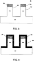
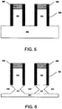
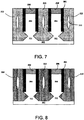
- FIGS. 3-11 are simplified cross-sectional view diagrams illustrating a number of stages of the manufacturing process of a semiconductor device according to an embodiment of the invention.
- the method of forming a semiconductor device includes, at step 201, providing a substrate structure having a semiconductor substrate and a fin structure on the semiconductor substrate.
- the fin structure includes a semiconductor layer and a hard mask layer on top of the semiconductor layer.
- the method also includes forming a spacer layer on sidewalls of the fin structure.
- the semiconductor substrate is etched to form recesses on both sides of the fin structure that extend partially to underneath the bottom of the fin structure.
- a filler material is formed to fill at least the recesses, thereby forming the first filler layer.
- a substrate structure 30 has a semiconductor substrate 302 and a fin structure 303 on the semiconductor substrate. Fin structure 303 includes a semiconductor layer 304 and a hard mask layer 306 on top of the semiconductor layer.
- Substrate 302 may be a semiconductor substrate, for example, a bulk silicon substrate. In some embodiments, substrate 302 can be a semiconductor material that is different from semiconductor layer 304 of the fin structure. For example, substrate 302 can be a silicon substrate, and semiconductor layer 304 of the fin structure can include germanium or silicon germanium.
- Hard mask layer 306 may be a silicon nitride, or other suitable masking material. Substrate structure 30 can be formed using known processes that will not be described in detail.
- an insulation material layer 308 is formed on fin structures 303 and substrate 302. As shown in FIG. 5 , insulation material layer 308 is etched to form spacers 501. Spacers 501 may be formed with silicon oxides or silicon nitrides, etc.
- substrate 302 is etched using hard mask layer 306 and spacers 501 as a mask to form recesses 310 in substrate 302. It can be seen that portions of recesses 310 extend to under fin structures 303. The remaining portions of substrate 302 underneath fins 304 are labeled 311.
- etching of the substrate 302 may be achieved using a crystalline orientation selective etching process.
- TMAH tetramethylammonium hydroxide
- TMAH tetramethyl ammonium hydroxide
- FIG. 6 the recesses formed in FIG. 6 are shown having E-shaped edges, it should be understood that it is only an example, as the present invention is not limited in concave shape.
- an isotropic wet etch process can be used to etch substrate 302 to form recesses 501.
- an insulating filler material is formed to fill recesses 310 to form a first filler layer 312.
- the insulating filler can be selected oxides of silicon, silicon-containing organic compounds, and other low-k dielectric materials, etc.
- a low-k dielectric material refers to a material having a dielectric constant of less than or equal to 3.0.
- a silicon-containing organic compound is used to fill recesses 310 to form the first filler layer 312.
- the organic silicon compound includes, but is not limited to, SiOCH.
- the first filler layer 312 fills at least recesses 310, and first filler layer 312 may be formed to be substantially flush with the top of hardmask layer 306, or may be formed so as to cover hard mask layer 306. When the first filler layer 312 covers hardmask layer 306, the portions of the cover may be etched away.
- First filler layer 312 may be formed using a plasma-enhanced chemical vapor deposition (PECVD) process or a spin coating process. As shown in FIG. 7 , first filler layer 312 may have voids 313.
- PECVD plasma-enhanced chemical vapor deposition
- the method includes curing first filler layer 312 to form a cured second filler layer 314, as shown in FIG. 8 .
- the first filler layer 312 with SiOCH material may be cured by a UV curing process to obtain a second filler layer 314 of porous SiOCH material. Because of its porosity, the equivalent dielectric constant is reduced further.
- the porosity of the second layer with ultraviolet-curing treatment can be 15% to 70%, so that the isolation structure can have low permittivity, high mechanical strength, excellent electrical properties and thermal stability.
- the material in second filler layer 314 can be oxidized to form an oxide of silicon.
- the second filler material 314 may be a porous silicon oxide layer. Further, the remaining portions 311 in the substrate under fin structures 303 can also be oxidized.
- the porous silicon oxide layer can be formed using wet oxidation and / or dry oxidation processes.
- the remaining portions 311 of the substrate may be partially oxidized or fully oxidized.
- the resulting isolation structure may have a low dielectric constant and good mechanical strength, so that the device has good electrical properties and thermal stability, thereby reducing the leakage current.
- second filler layer 314 can be etched, thereby forming the isolation structure 316 in the recessed regions 310.
- the second filler layer 314 of FIG. 8 is etched back before it is oxidized.
- second filler layer 314 can be etched back using, e.g., dilute aqueous hydrofluoric acid, thereby removing a portion of second filler layer 314, so that at least a portion of the spacer layer 501 at the side walls of fin 313 is exposed.
- a wet oxidation and / or dry oxidation process can be used to oxidize the porous filler layer 314 and the recesses substrate 311.
- the recessed portion 311 may be partially oxidized to silicon oxides, or fully oxidized to silicon oxides.
- the exposed barrier or spacer layer 501 may be removed to expose at least a portion of the fin, resulting in the structure shown in FIG. 11 .
- the dielectric constant of isolation structure 316 (or equivalent dielectric constant) is low.
- the device can be well isolated with good mechanical strength.
- the device can also have excellent stability and electrical characteristics (e.g., thermal stability, etc.), and the leakage current can be reduced.
- embodiments of the present invention also provide a semiconductor device as shown in FIG. 11 .
- the semiconductor device includes a semiconductor substrate and a fin structure on the semiconductor substrate.
- the fin structure includes a semiconductor layer.
- the semiconductor device also includes recesses in the semiconductor substrate on both sides of the fin structure and extending partially to underneath the bottom of the fin structure.
- the semiconductor device also includes an isolation structure filling the recesses.
- the isolation structure comprises a porous silicon oxide material.
- the isolation structure includes a low K dielectric material.
- the porosity of the isolation structure is between 15% to 70%.
- the semiconductor substrate also includes an additional semiconductor layer adjacent to the semiconductor substrate, and the recesses are formed in the additional semiconductor layer.
- the device also includes a silicon oxide material under the fin structure and between the recesses.
- the device also has a hard mask layer on the semiconductor material of the fin structure.
Landscapes
- Element Separation (AREA)
- Insulated Gate Type Field-Effect Transistor (AREA)
- Chemical & Material Sciences (AREA)
- Chemical Kinetics & Catalysis (AREA)
- General Chemical & Material Sciences (AREA)
Abstract
Description
- This application claims priority to Chinese patent application No.
201610191184.3, filed on March 30, 2016 - The present invention relates to the field of semiconductor technology. Specifically, embodiments of the invention relate to fin type device structures and manufacturing methods.
-
FIG. 1 is a cross-sectional view illustrating a conventional fin type device (e.g., the FinFET device). The device includes asubstrate 102 and a fin structure on the substrate. The fin structure includes asemiconductor layer 104 and ahard mask layer 106 overlying the semiconductor layer. In this conventional structure, the fin structures are separated by anisolation layer 108. Since theinsulating layer 108 exists only between parts of thesemiconductor layer 104 of the fin, there is no effective isolation in thesubstrate 102 below the fin structures. As a result, this structure can be susceptible to the problem of leakage current. - The above problems are more pronounced in the bulk semiconductor substrate process. Regarding the DC characteristics of the semiconductor device, devices based on the SOI (Silicon-On-Insulator) substrate and bulk silicon FinFET device of similar device sizes can provide similar on/off current ratio. However, regarding PN junction leakage current and parasitic capacitance of the devices, the difference becomes significant.
- It is an object of the present invention to provide an improved method of forming a semiconductor device and a corresponding semiconductor device by which at least some of the afore-mentioned problems are overcome or reduced.
- The object is achieved by the features of the respective independent claims. Further embodiments are defined in the respective dependent claims.
- A first aspect of the invention provides a method of forming a semiconductor device. The method includes providing a substrate structure having a semiconductor substrate and a fin structure on the semiconductor substrate. The fin structure includes a semiconductor layer and a hard mask layer on top of the semiconductor layer. The method also includes forming a spacer layer on sidewalls of the fin structure. Next, using the hard mask layer and the spacer layer as a mask, the semiconductor substrate is etched to form recesses on both sides of the fin structure that extend partially to underneath the bottom of the fin structure. The method further includes forming a filler material to fill at least the recesses, thereby forming the first filler layer.
- Preferably, the filler material includes an organic silicon compound, and the method also includes curing the first filler layer to form a cured second filler layer. The second filler layer may be oxidized to form a porous silicon oxide material.
- Preferably, the method also includes oxidizing the portion of the semiconductor substrate underneath the fin structure and between the recesses.
- Preferably, the first filler layer may include voids.
- Preferably, the organic silicon compound comprises SiOCH (organosilicate).
- Preferably, the second filler layer has a porosity of 15% to 70%
- Preferably, oxidizing the second filler layer includes using wet oxidation and / or dry oxidation.
- Preferably, the method also includes etching the porous silicon oxide material to expose at least a portion of the spacer layer, and removing the spacer layer to expose a portion of the fin structure.
- Preferably, etching the semiconductor substrate to form recesses includes using an isotropic etching process.
- Preferably, etching the semiconductor substrate to form recesses comprises using a crystalline orientation selective wet etching process.
- Preferably, forming a spacer layer on sidewalls of the fin structure includes forming a spacer material layer overlying the fin structure, and removing the spacer material layer from the top of the fin structure and the silicon substrate to form the spacer layer on sidewalls of the fin structure.
- Preferably, the semiconductor substrate also includes an additional semiconductor layer adjacent to the semiconductor substrate, and the recesses are formed in the additional semiconductor layer.
- A second aspect of the invention provides a semiconductor device. The semiconductor device includes a semiconductor substrate and a fin structure on the semiconductor substrate. The fin structure includes a semiconductor layer. The semiconductor device also includes recesses in the semiconductor substrate on both sides of the fin structure and extending partially to underneath the bottom of the fin structure. The semiconductor device also includes an isolation structure filling the recesses.
- Preferably, the isolation structure comprises a porous silicon oxide material.
- Preferably, the isolation structure includes a low K dielectric material.
- Preferably, the porosity of the isolation structure is between 15% to 70%.
- Preferably, the semiconductor substrate also includes an additional semiconductor layer adjacent to the semiconductor substrate, and the recesses are formed in the additional semiconductor layer.
- Preferably, the device also includes a silicon oxide material under the fin structure and between the recesses.
- Preferably, the device also has a hard mask layer on the semiconductor material of the fin structure.
- The semiconductor device according to the second aspect of the invention can be obtained by a method according to the first aspect of the invention.
- The following description, together with the accompanying drawings, will provide further understanding of the nature and advantages of the claimed invention.
-
-
FIG. 1 is a cross-sectional view illustrating a conventional fin type device (e.g., the FinFET device); -
FIG. 2 is a simplified flow chart illustrating a method of manufacturing a semiconductor device according to an embodiment of the invention; and -
FIGS. 3-11 are simplified cross-sectional view diagrams illustrating a number of stages of the manufacturing process of a semiconductor device according to an embodiment of the invention. - The drawings of various exemplary embodiments of the present invention will be described in detail. It should be noted that, unless otherwise specified, the relative arrangement set forth in these embodiments, components and steps, the numerical expressions, and values do not limit the scope of the present invention. At the same time, it should be appreciated that, for ease of description, the dimensions of the various parts are not illustrated in the drawings according to the actual proportional relationship.
- The following description of exemplary embodiments is merely illustrative of the present invention and in no way presents any restrictions on its use or application. Techniques, methods, and equipment known to someone of ordinary skill in the relevant art may not be discussed in detail, but in appropriate cases, the techniques, methods and equipment should be considered as part of the specification.
- In all the examples shown and discussed, any specific value is to be construed as merely illustrative, and not as a limitation. Accordingly, another exemplary embodiment may have different values. It should be also noted that like reference numerals and letters refer to similar items in the following figures, and thus once an item is defined in one figure, it need not be further discussed in subsequent figures.
-
FIG. 2 is a simplified flow chart illustrating a method of manufacturing a semiconductor device according to an embodiment of the invention.FIGS. 3-11 are simplified cross-sectional view diagrams illustrating a number of stages of the manufacturing process of a semiconductor device according to an embodiment of the invention. - As shown in
FIG. 2 , the method of forming a semiconductor device includes, atstep 201, providing a substrate structure having a semiconductor substrate and a fin structure on the semiconductor substrate. The fin structure includes a semiconductor layer and a hard mask layer on top of the semiconductor layer. Atstep 203, the method also includes forming a spacer layer on sidewalls of the fin structure. Next, atstep 205, using the hard mask layer and the spacer layer as a mask, the semiconductor substrate is etched to form recesses on both sides of the fin structure that extend partially to underneath the bottom of the fin structure. Atstep 207, a filler material is formed to fill at least the recesses, thereby forming the first filler layer. - The method is further described in
FIGS. 3-11 , which are simplified cross-sectional view diagrams illustrating a number of stages of the manufacturing process of a semiconductor device according to an embodiment of the invention. As shown inFIG. 3 , asubstrate structure 30 has asemiconductor substrate 302 and afin structure 303 on the semiconductor substrate.Fin structure 303 includes asemiconductor layer 304 and ahard mask layer 306 on top of the semiconductor layer.Substrate 302 may be a semiconductor substrate, for example, a bulk silicon substrate. In some embodiments,substrate 302 can be a semiconductor material that is different fromsemiconductor layer 304 of the fin structure. For example,substrate 302 can be a silicon substrate, andsemiconductor layer 304 of the fin structure can include germanium or silicon germanium.Hard mask layer 306 may be a silicon nitride, or other suitable masking material.Substrate structure 30 can be formed using known processes that will not be described in detail. - In
FIG. 4 , aninsulation material layer 308 is formed onfin structures 303 andsubstrate 302. As shown inFIG. 5 ,insulation material layer 308 is etched to formspacers 501.Spacers 501 may be formed with silicon oxides or silicon nitrides, etc. - In
FIG. 6 ,substrate 302 is etched usinghard mask layer 306 andspacers 501 as a mask to formrecesses 310 insubstrate 302. It can be seen that portions ofrecesses 310 extend to underfin structures 303. The remaining portions ofsubstrate 302 underneathfins 304 are labeled 311. - In an embodiment, etching of the
substrate 302 may be achieved using a crystalline orientation selective etching process. For example, tetramethylammonium hydroxide (Tetramethyl ammonium hydroxide, referred to as TMAH) solution may be used to etchsubstrate 302 fromrecesses 310. Although the recesses formed inFIG. 6 are shown having E-shaped edges, it should be understood that it is only an example, as the present invention is not limited in concave shape. For example, an isotropic wet etch process can be used to etchsubstrate 302 to form recesses 501. - In
step 207 inFIG. 2 , an insulating filler material is formed to fillrecesses 310 to form afirst filler layer 312. The insulating filler can be selected oxides of silicon, silicon-containing organic compounds, and other low-k dielectric materials, etc. As used here, a low-k dielectric material refers to a material having a dielectric constant of less than or equal to 3.0. Thus, a novel isolation structure for the fin device can be realized, providing good support, good mechanical strength, good electrical properties and stability. - In some embodiments, a silicon-containing organic compound is used to fill
recesses 310 to form thefirst filler layer 312. The organic silicon compound includes, but is not limited to, SiOCH. Thefirst filler layer 312 fills atleast recesses 310, andfirst filler layer 312 may be formed to be substantially flush with the top ofhardmask layer 306, or may be formed so as to coverhard mask layer 306. When thefirst filler layer 312 covershardmask layer 306, the portions of the cover may be etched away.First filler layer 312 may be formed using a plasma-enhanced chemical vapor deposition (PECVD) process or a spin coating process. As shown inFIG. 7 ,first filler layer 312 may havevoids 313. - Next, the method includes curing
first filler layer 312 to form a curedsecond filler layer 314, as shown inFIG. 8 . For example, thefirst filler layer 312 with SiOCH material may be cured by a UV curing process to obtain asecond filler layer 314 of porous SiOCH material. Because of its porosity, the equivalent dielectric constant is reduced further. In one implementation, the porosity of the second layer with ultraviolet-curing treatment can be 15% to 70%, so that the isolation structure can have low permittivity, high mechanical strength, excellent electrical properties and thermal stability. - In certain embodiments, as shown in
FIG. 9 , the material insecond filler layer 314 can be oxidized to form an oxide of silicon. Thesecond filler material 314 may be a porous silicon oxide layer. Further, the remainingportions 311 in the substrate underfin structures 303 can also be oxidized. - In one embodiment, the porous silicon oxide layer can be formed using wet oxidation and / or dry oxidation processes. The remaining
portions 311 of the substrate may be partially oxidized or fully oxidized. The resulting isolation structure may have a low dielectric constant and good mechanical strength, so that the device has good electrical properties and thermal stability, thereby reducing the leakage current. - Subsequently, in some embodiments, as shown in
FIG. 10 ,second filler layer 314 can be etched, thereby forming theisolation structure 316 in the recessedregions 310. - In another embodiment, the
second filler layer 314 ofFIG. 8 is etched back before it is oxidized. For example,second filler layer 314 can be etched back using, e.g., dilute aqueous hydrofluoric acid, thereby removing a portion ofsecond filler layer 314, so that at least a portion of thespacer layer 501 at the side walls offin 313 is exposed. After that, a wet oxidation and / or dry oxidation process can be used to oxidize theporous filler layer 314 and therecesses substrate 311. Here, the recessedportion 311 may be partially oxidized to silicon oxides, or fully oxidized to silicon oxides. Finally, the exposed barrier orspacer layer 501 may be removed to expose at least a portion of the fin, resulting in the structure shown inFIG. 11 . According to an embodiment of the present invention, the dielectric constant of isolation structure 316 (or equivalent dielectric constant) is low. The device can be well isolated with good mechanical strength. The device can also have excellent stability and electrical characteristics (e.g., thermal stability, etc.), and the leakage current can be reduced. - In alternative embodiments, embodiments of the present invention also provide a semiconductor device as shown in
FIG. 11 . The semiconductor device includes a semiconductor substrate and a fin structure on the semiconductor substrate. The fin structure includes a semiconductor layer. The semiconductor device also includes recesses in the semiconductor substrate on both sides of the fin structure and extending partially to underneath the bottom of the fin structure. The semiconductor device also includes an isolation structure filling the recesses. - In an embodiment of the above device, the isolation structure comprises a porous silicon oxide material.
- In another embodiment, the isolation structure includes a low K dielectric material.
- In another embodiment, the porosity of the isolation structure is between 15% to 70%.
- In another embodiment, the semiconductor substrate also includes an additional semiconductor layer adjacent to the semiconductor substrate, and the recesses are formed in the additional semiconductor layer.
- In another embodiment, the device also includes a silicon oxide material under the fin structure and between the recesses.
- In another embodiment, the device also has a hard mask layer on the semiconductor material of the fin structure.
Claims (15)
- A method of forming a semiconductor device, comprising:providing a substrate structure, the substrate structure including a semiconductor substrate and a fin structure on the semiconductor substrate, said fin structure including a semiconductor layer and a hard mask layer on top of the semiconductor layer;forming a spacer layer on sidewalls of the fin structure;using the hard mask layer and the spacer layer as a mask, etching the semiconductor substrate to form recesses on both sides of the fin structure, the recesses extending partially to underneath the bottom of the fin structure; andforming a filler material to fill at least the recesses, thereby forming the first filler layer.
- The method of claim 1, wherein the filler material comprises an organic silicon compound, and the method further comprising:curing said first filler layer to form a cured second filler layer; andoxidizing the second filler layer to form a porous silicon oxide material.
- The method of claim 2, further comprising at least one of:oxidizing the portion of the semiconductor substrate underneath the fin structure and between the recesses; and/oroxidizing the second filler layer comprises using wet oxidation and/or dry oxidation, wherein a portion of the semiconductor under the fin structure is partially or fully oxidized; andetching the porous silicon oxide material to expose at least a portion of the spacer layer, and removing the spacer layer to expose a portion of the fin structure.
- The method of claim 2 or 3, wherein the method is characterized by at least one of:the first filler layer comprises voids;the organic silicon compound comprises organosilicate, SiOCH;the second filler layer has a porosity of 15% to 70%; andthe porous silicon oxide material comprises silicon dioxide.
- The method of any one of the claims 1-4, wherein etching the semiconductor substrate to form recesses comprises using an isotropic etching process.
- The method of any one of the claims 1-5, wherein etching the semiconductor substrate to form recesses comprises using crystalline orientation selective wet etching process.
- The method of any one of the claim 1-6, wherein forming a spacer layer on sidewalls of the fin structure comprises:forming a spacer material layer overlying the fin structure; andremoving the spacer material layer from the top of the fin structure and the silicon substrate to form the spacer layer on sidewalls of the fin structure.
- The method of any one of the claim 1-7, wherein the semiconductor substrate further comprises an additional semiconductor layer adjacent to the semiconductor substrate, and the recesses are formed in the additional semiconductor layer.
- A semiconductor device, comprising:a semiconductor substrate and a fin structure on the semiconductor substrate, said fin structure including a semiconductor layer;recesses in the semiconductor substrate on both sides of the fin structure, and extending partially to underneath the bottom of the fin structure; andan isolation structure filling the recesses.
- The device of claim 9, wherein the isolation structure comprises a porous silicon oxide material.
- The device of claim 9 or 10, wherein the isolation structure comprises a low K dielectric material.
- The device of any one of the claims 9-11, wherein the porosity of the isolation structure is between 15% to 70%.
- The device of any one of the claims 9-12, wherein the semiconductor substrate further comprises an additional semiconductor layer adjacent to the semiconductor substrate, and the recesses are formed in the additional semiconductor layer.
- The device of claim 9-13, further comprising a silicon oxide material under the fin structure and between the recesses.
- The device of claim 9-14, further comprising a hard mask layer on the semiconductor material of the fin structure.
Applications Claiming Priority (1)
| Application Number | Priority Date | Filing Date | Title |
|---|---|---|---|
| CN201610191184.3A CN107293588A (en) | 2016-03-30 | 2016-03-30 | Semiconductor device and its manufacture method |
Publications (1)
| Publication Number | Publication Date |
|---|---|
| EP3226302A1 true EP3226302A1 (en) | 2017-10-04 |
Family
ID=58412918
Family Applications (1)
| Application Number | Title | Priority Date | Filing Date |
|---|---|---|---|
| EP17162505.6A Withdrawn EP3226302A1 (en) | 2016-03-30 | 2017-03-23 | Method for fabricating finfet structure |
Country Status (3)
| Country | Link |
|---|---|
| US (2) | US10084092B2 (en) |
| EP (1) | EP3226302A1 (en) |
| CN (1) | CN107293588A (en) |
Families Citing this family (4)
| Publication number | Priority date | Publication date | Assignee | Title |
|---|---|---|---|---|
| CN107293588A (en) | 2016-03-30 | 2017-10-24 | 中芯国际集成电路制造(上海)有限公司 | Semiconductor device and its manufacture method |
| US10325811B2 (en) * | 2017-10-26 | 2019-06-18 | Globalfoundries Inc. | Field-effect transistors with fins having independently-dimensioned sections |
| US11217664B2 (en) * | 2020-02-11 | 2022-01-04 | Nanya Technology Corporation | Semiconductor device with porous dielectric structure |
| CN111599684B (en) * | 2020-05-25 | 2023-08-15 | 上海华力集成电路制造有限公司 | Fin body manufacturing method, fin field effect transistor and a fin body structure |
Citations (7)
| Publication number | Priority date | Publication date | Assignee | Title |
|---|---|---|---|---|
| EP1037275A1 (en) * | 1999-03-17 | 2000-09-20 | Canon Sales Co., Inc. | Method for forming a porous silicon oxide film |
| US20110084340A1 (en) * | 2009-10-14 | 2011-04-14 | Feng Yuan | Voids in STI Regions for Forming Bulk FinFETs |
| US20110095372A1 (en) * | 2009-10-28 | 2011-04-28 | Taiwan Semiconductor Manufacturing Company, Ltd. | Forming Inter-Device STI Regions and Intra-Device STI Regions Using Different Dielectric Materials |
| US20120299099A1 (en) * | 2011-05-26 | 2012-11-29 | Rai-Min Huang | Finfet transistor structure and method for making the same |
| WO2013095384A1 (en) * | 2011-12-20 | 2013-06-27 | Intel Corporation | Semiconductor device with isolated body portion |
| US20150162190A1 (en) * | 2013-11-25 | 2015-06-11 | Commissariat A L'energie Atomique Et Aux Ene Alt | Method for forming spacers for a transistor gate |
| CN102651305B (en) * | 2011-02-25 | 2015-09-30 | 中国科学院微电子研究所 | A kind of preparation method of Ω-shaped fin |
Family Cites Families (7)
| Publication number | Priority date | Publication date | Assignee | Title |
|---|---|---|---|---|
| US8106459B2 (en) * | 2008-05-06 | 2012-01-31 | Taiwan Semiconductor Manufacturing Company, Ltd. | FinFETs having dielectric punch-through stoppers |
| US8143121B2 (en) * | 2009-10-01 | 2012-03-27 | Nanya Technology Corp. | DRAM cell with double-gate fin-FET, DRAM cell array and fabrication method thereof |
| CN102623321B (en) * | 2012-03-31 | 2015-01-28 | 上海华力微电子有限公司 | Manufacture method of longitudinal stacking type rear-grid type SiNWFET (Silicon-Nanowire Field Effect Transistor) based on bulk silicon |
| CN103700593B (en) * | 2013-12-18 | 2016-02-17 | 北京大学 | Prepare the method for accurate SOI source and drain multi-gate device |
| US9472446B2 (en) * | 2014-06-18 | 2016-10-18 | Globalfoundries Inc. | Methods of forming a FinFET semiconductor device with a unique gate configuration, and the resulting FinFET device |
| CN106298921B (en) * | 2015-06-01 | 2019-07-02 | 中芯国际集成电路制造(上海)有限公司 | Semiconductor device, fin field effect transistor and method of forming the same |
| CN107293588A (en) | 2016-03-30 | 2017-10-24 | 中芯国际集成电路制造(上海)有限公司 | Semiconductor device and its manufacture method |
-
2016
- 2016-03-30 CN CN201610191184.3A patent/CN107293588A/en active Pending
-
2017
- 2017-01-03 US US15/397,584 patent/US10084092B2/en active Active
- 2017-03-23 EP EP17162505.6A patent/EP3226302A1/en not_active Withdrawn
-
2018
- 2018-08-21 US US16/106,613 patent/US10608112B2/en active Active
Patent Citations (7)
| Publication number | Priority date | Publication date | Assignee | Title |
|---|---|---|---|---|
| EP1037275A1 (en) * | 1999-03-17 | 2000-09-20 | Canon Sales Co., Inc. | Method for forming a porous silicon oxide film |
| US20110084340A1 (en) * | 2009-10-14 | 2011-04-14 | Feng Yuan | Voids in STI Regions for Forming Bulk FinFETs |
| US20110095372A1 (en) * | 2009-10-28 | 2011-04-28 | Taiwan Semiconductor Manufacturing Company, Ltd. | Forming Inter-Device STI Regions and Intra-Device STI Regions Using Different Dielectric Materials |
| CN102651305B (en) * | 2011-02-25 | 2015-09-30 | 中国科学院微电子研究所 | A kind of preparation method of Ω-shaped fin |
| US20120299099A1 (en) * | 2011-05-26 | 2012-11-29 | Rai-Min Huang | Finfet transistor structure and method for making the same |
| WO2013095384A1 (en) * | 2011-12-20 | 2013-06-27 | Intel Corporation | Semiconductor device with isolated body portion |
| US20150162190A1 (en) * | 2013-11-25 | 2015-06-11 | Commissariat A L'energie Atomique Et Aux Ene Alt | Method for forming spacers for a transistor gate |
Also Published As
| Publication number | Publication date |
|---|---|
| US10084092B2 (en) | 2018-09-25 |
| CN107293588A (en) | 2017-10-24 |
| US10608112B2 (en) | 2020-03-31 |
| US20180358461A1 (en) | 2018-12-13 |
| US20170288049A1 (en) | 2017-10-05 |
Similar Documents
| Publication | Publication Date | Title |
|---|---|---|
| KR102073395B1 (en) | A method of manufacturing a semiconductor device with separated merged source/drain structure | |
| US8383503B2 (en) | Methods for forming semiconductor structures using selectively-formed sidewall spacers | |
| US8846466B2 (en) | Forming inter-device STI regions and intra-device STI regions using different dielectric materials | |
| CN109427674B (en) | Methods of forming fin field effect transistor device structures | |
| KR101745155B1 (en) | Semiconductor device and manufacturing method thereof | |
| US10608112B2 (en) | FinFET device having FinFET structure and filled recesses that partially extend underneath the Fin structure | |
| CN103985711A (en) | FinFETs with reduced parasitic capacitance and methods of forming the same | |
| WO2018040865A1 (en) | Vdmos device and manufacturing method therefor | |
| US9299793B2 (en) | Semiconductor device with a field plate trench having a thick bottom dielectric | |
| US9385037B2 (en) | Semiconductor arrangement comprising metal cap and dielectric layer defining air gap | |
| US8673723B1 (en) | Methods of forming isolation regions for FinFET semiconductor devices | |
| US20170330933A1 (en) | Air gaps formed by porous silicon removal | |
| US20130224944A1 (en) | Methods for fabricating integrated circuits using tailored chamfered gate liner profiles | |
| US8501578B2 (en) | Semiconductor structure formed without requiring thermal oxidation | |
| CN108091611B (en) | Semiconductor device and method of manufacturing the same | |
| CN103035709B (en) | A kind of semiconductor structure and its manufacturing method | |
| US9660058B2 (en) | Method of FinFET formation | |
| US11798836B2 (en) | Semiconductor isolation structure and method of making the same | |
| CN103681275B (en) | A kind of semiconductor device with highly controllable fin and preparation method | |
| US9437674B2 (en) | Insulating trench forming method | |
| CN109427808B (en) | Semiconductor memory element and method of manufacturing the same | |
| US20170076976A1 (en) | Isolation structure and method for fabricating the same | |
| CN111916398B (en) | A method of manufacturing a semiconductor device | |
| CN113394270B (en) | Isolation structure of semiconductor device and manufacturing method thereof | |
| US20120261790A1 (en) | Substrate structure, semiconductor device, and method for manufacturing the same |
Legal Events
| Date | Code | Title | Description |
|---|---|---|---|
| PUAI | Public reference made under article 153(3) epc to a published international application that has entered the european phase |
Free format text: ORIGINAL CODE: 0009012 |
|
| STAA | Information on the status of an ep patent application or granted ep patent |
Free format text: STATUS: THE APPLICATION HAS BEEN PUBLISHED |
|
| AK | Designated contracting states |
Kind code of ref document: A1 Designated state(s): AL AT BE BG CH CY CZ DE DK EE ES FI FR GB GR HR HU IE IS IT LI LT LU LV MC MK MT NL NO PL PT RO RS SE SI SK SM TR |
|
| AX | Request for extension of the european patent |
Extension state: BA ME |
|
| STAA | Information on the status of an ep patent application or granted ep patent |
Free format text: STATUS: REQUEST FOR EXAMINATION WAS MADE |
|
| 17P | Request for examination filed |
Effective date: 20180112 |
|
| RBV | Designated contracting states (corrected) |
Designated state(s): AL AT BE BG CH CY CZ DE DK EE ES FI FR GB GR HR HU IE IS IT LI LT LU LV MC MK MT NL NO PL PT RO RS SE SI SK SM TR |
|
| RAP1 | Party data changed (applicant data changed or rights of an application transferred) |
Owner name: SEMICONDUCTOR MANUFACTURING INTERNATIONAL (BEIJING Owner name: SEMICONDUCTOR MANUFACTURING INTERNATIONAL (SHANGHA |
|
| STAA | Information on the status of an ep patent application or granted ep patent |
Free format text: STATUS: EXAMINATION IS IN PROGRESS |
|
| 17Q | First examination report despatched |
Effective date: 20200508 |
|
| STAA | Information on the status of an ep patent application or granted ep patent |
Free format text: STATUS: THE APPLICATION IS DEEMED TO BE WITHDRAWN |
|
| 18D | Application deemed to be withdrawn |
Effective date: 20200919 |