EP3226287A1 - Electronic device - Google Patents
Electronic device Download PDFInfo
- Publication number
- EP3226287A1 EP3226287A1 EP15863142.4A EP15863142A EP3226287A1 EP 3226287 A1 EP3226287 A1 EP 3226287A1 EP 15863142 A EP15863142 A EP 15863142A EP 3226287 A1 EP3226287 A1 EP 3226287A1
- Authority
- EP
- European Patent Office
- Prior art keywords
- conductive layer
- metal plate
- power element
- electronic device
- heat dissipation
- Prior art date
- Legal status (The legal status is an assumption and is not a legal conclusion. Google has not performed a legal analysis and makes no representation as to the accuracy of the status listed.)
- Granted
Links
Images
Classifications
-
- H—ELECTRICITY
- H05—ELECTRIC TECHNIQUES NOT OTHERWISE PROVIDED FOR
- H05K—PRINTED CIRCUITS; CASINGS OR CONSTRUCTIONAL DETAILS OF ELECTRIC APPARATUS; MANUFACTURE OF ASSEMBLAGES OF ELECTRICAL COMPONENTS
- H05K7/00—Constructional details common to different types of electric apparatus
- H05K7/20—Modifications to facilitate cooling, ventilating, or heating
- H05K7/2089—Modifications to facilitate cooling, ventilating, or heating for power electronics, e.g. for inverters for controlling motor
- H05K7/20927—Liquid coolant without phase change
-
- H—ELECTRICITY
- H02—GENERATION; CONVERSION OR DISTRIBUTION OF ELECTRIC POWER
- H02M—APPARATUS FOR CONVERSION BETWEEN AC AND AC, BETWEEN AC AND DC, OR BETWEEN DC AND DC, AND FOR USE WITH MAINS OR SIMILAR POWER SUPPLY SYSTEMS; CONVERSION OF DC OR AC INPUT POWER INTO SURGE OUTPUT POWER; CONTROL OR REGULATION THEREOF
- H02M7/00—Conversion of AC power input into DC power output; Conversion of DC power input into AC power output
- H02M7/003—Constructional details, e.g. physical layout, assembly, wiring or busbar connections
-
- H—ELECTRICITY
- H02—GENERATION; CONVERSION OR DISTRIBUTION OF ELECTRIC POWER
- H02M—APPARATUS FOR CONVERSION BETWEEN AC AND AC, BETWEEN AC AND DC, OR BETWEEN DC AND DC, AND FOR USE WITH MAINS OR SIMILAR POWER SUPPLY SYSTEMS; CONVERSION OF DC OR AC INPUT POWER INTO SURGE OUTPUT POWER; CONTROL OR REGULATION THEREOF
- H02M7/00—Conversion of AC power input into DC power output; Conversion of DC power input into AC power output
- H02M7/42—Conversion of DC power input into AC power output without possibility of reversal
-
- H—ELECTRICITY
- H05—ELECTRIC TECHNIQUES NOT OTHERWISE PROVIDED FOR
- H05K—PRINTED CIRCUITS; CASINGS OR CONSTRUCTIONAL DETAILS OF ELECTRIC APPARATUS; MANUFACTURE OF ASSEMBLAGES OF ELECTRICAL COMPONENTS
- H05K1/00—Printed circuits
- H05K1/02—Details
-
- H—ELECTRICITY
- H05—ELECTRIC TECHNIQUES NOT OTHERWISE PROVIDED FOR
- H05K—PRINTED CIRCUITS; CASINGS OR CONSTRUCTIONAL DETAILS OF ELECTRIC APPARATUS; MANUFACTURE OF ASSEMBLAGES OF ELECTRICAL COMPONENTS
- H05K1/00—Printed circuits
- H05K1/02—Details
- H05K1/0201—Thermal arrangements, e.g. for cooling, heating or preventing overheating
- H05K1/0203—Cooling of mounted components
- H05K1/0207—Cooling of mounted components using internal conductor planes parallel to the surface for thermal conduction, e.g. power planes
-
- H—ELECTRICITY
- H05—ELECTRIC TECHNIQUES NOT OTHERWISE PROVIDED FOR
- H05K—PRINTED CIRCUITS; CASINGS OR CONSTRUCTIONAL DETAILS OF ELECTRIC APPARATUS; MANUFACTURE OF ASSEMBLAGES OF ELECTRICAL COMPONENTS
- H05K1/00—Printed circuits
- H05K1/02—Details
- H05K1/0201—Thermal arrangements, e.g. for cooling, heating or preventing overheating
- H05K1/0203—Cooling of mounted components
- H05K1/021—Components thermally connected to metal substrates or heat-sinks by insert mounting
-
- H—ELECTRICITY
- H05—ELECTRIC TECHNIQUES NOT OTHERWISE PROVIDED FOR
- H05K—PRINTED CIRCUITS; CASINGS OR CONSTRUCTIONAL DETAILS OF ELECTRIC APPARATUS; MANUFACTURE OF ASSEMBLAGES OF ELECTRICAL COMPONENTS
- H05K1/00—Printed circuits
- H05K1/18—Printed circuits structurally associated with non-printed electric components
-
- H—ELECTRICITY
- H05—ELECTRIC TECHNIQUES NOT OTHERWISE PROVIDED FOR
- H05K—PRINTED CIRCUITS; CASINGS OR CONSTRUCTIONAL DETAILS OF ELECTRIC APPARATUS; MANUFACTURE OF ASSEMBLAGES OF ELECTRICAL COMPONENTS
- H05K1/00—Printed circuits
- H05K1/18—Printed circuits structurally associated with non-printed electric components
- H05K1/182—Printed circuits structurally associated with non-printed electric components associated with components mounted in printed circuit boards [PCB], e.g. insert-mounted components [IMC]
- H05K1/185—Printed circuits structurally associated with non-printed electric components associated with components mounted in printed circuit boards [PCB], e.g. insert-mounted components [IMC] associated with components encapsulated in the insulating substrate of the PCBs; associated with components incorporated in internal layers of multilayer circuit boards
-
- H—ELECTRICITY
- H05—ELECTRIC TECHNIQUES NOT OTHERWISE PROVIDED FOR
- H05K—PRINTED CIRCUITS; CASINGS OR CONSTRUCTIONAL DETAILS OF ELECTRIC APPARATUS; MANUFACTURE OF ASSEMBLAGES OF ELECTRICAL COMPONENTS
- H05K3/00—Apparatus or processes for manufacturing printed circuits
- H05K3/46—Manufacturing multilayer circuits
- H05K3/4697—Manufacturing multilayer circuits having cavities, e.g. for mounting components
-
- H—ELECTRICITY
- H05—ELECTRIC TECHNIQUES NOT OTHERWISE PROVIDED FOR
- H05K—PRINTED CIRCUITS; CASINGS OR CONSTRUCTIONAL DETAILS OF ELECTRIC APPARATUS; MANUFACTURE OF ASSEMBLAGES OF ELECTRICAL COMPONENTS
- H05K7/00—Constructional details common to different types of electric apparatus
- H05K7/14—Mounting supporting structure in casing or on frame or rack
-
- H—ELECTRICITY
- H05—ELECTRIC TECHNIQUES NOT OTHERWISE PROVIDED FOR
- H05K—PRINTED CIRCUITS; CASINGS OR CONSTRUCTIONAL DETAILS OF ELECTRIC APPARATUS; MANUFACTURE OF ASSEMBLAGES OF ELECTRICAL COMPONENTS
- H05K7/00—Constructional details common to different types of electric apparatus
- H05K7/20—Modifications to facilitate cooling, ventilating, or heating
-
- H—ELECTRICITY
- H05—ELECTRIC TECHNIQUES NOT OTHERWISE PROVIDED FOR
- H05K—PRINTED CIRCUITS; CASINGS OR CONSTRUCTIONAL DETAILS OF ELECTRIC APPARATUS; MANUFACTURE OF ASSEMBLAGES OF ELECTRICAL COMPONENTS
- H05K7/00—Constructional details common to different types of electric apparatus
- H05K7/20—Modifications to facilitate cooling, ventilating, or heating
- H05K7/20218—Modifications to facilitate cooling, ventilating, or heating using a liquid coolant without phase change in electronic enclosures
- H05K7/20263—Heat dissipaters releasing heat from coolant
-
- H—ELECTRICITY
- H05—ELECTRIC TECHNIQUES NOT OTHERWISE PROVIDED FOR
- H05K—PRINTED CIRCUITS; CASINGS OR CONSTRUCTIONAL DETAILS OF ELECTRIC APPARATUS; MANUFACTURE OF ASSEMBLAGES OF ELECTRICAL COMPONENTS
- H05K7/00—Constructional details common to different types of electric apparatus
- H05K7/20—Modifications to facilitate cooling, ventilating, or heating
- H05K7/2039—Modifications to facilitate cooling, ventilating, or heating characterised by the heat transfer by conduction from the heat generating element to a dissipating body
- H05K7/20436—Inner thermal coupling elements in heat dissipating housings, e.g. protrusions or depressions integrally formed in the housing
-
- H—ELECTRICITY
- H10—SEMICONDUCTOR DEVICES; ELECTRIC SOLID-STATE DEVICES NOT OTHERWISE PROVIDED FOR
- H10W—GENERIC PACKAGES, INTERCONNECTIONS, CONNECTORS OR OTHER CONSTRUCTIONAL DETAILS OF DEVICES COVERED BY CLASS H10
- H10W20/00—Interconnections in chips, wafers or substrates
- H10W20/40—Interconnections external to wafers or substrates, e.g. back-end-of-line [BEOL] metallisations or vias connecting to gate electrodes
-
- H—ELECTRICITY
- H10—SEMICONDUCTOR DEVICES; ELECTRIC SOLID-STATE DEVICES NOT OTHERWISE PROVIDED FOR
- H10W—GENERIC PACKAGES, INTERCONNECTIONS, CONNECTORS OR OTHER CONSTRUCTIONAL DETAILS OF DEVICES COVERED BY CLASS H10
- H10W40/00—Arrangements for thermal protection or thermal control
- H10W40/40—Arrangements for thermal protection or thermal control involving heat exchange by flowing fluids
- H10W40/47—Arrangements for thermal protection or thermal control involving heat exchange by flowing fluids by flowing liquids, e.g. forced water cooling
-
- H—ELECTRICITY
- H10—SEMICONDUCTOR DEVICES; ELECTRIC SOLID-STATE DEVICES NOT OTHERWISE PROVIDED FOR
- H10W—GENERIC PACKAGES, INTERCONNECTIONS, CONNECTORS OR OTHER CONSTRUCTIONAL DETAILS OF DEVICES COVERED BY CLASS H10
- H10W70/00—Package substrates; Interposers; Redistribution layers [RDL]
- H10W70/01—Manufacture or treatment
- H10W70/05—Manufacture or treatment of insulating or insulated package substrates, or of interposers, or of redistribution layers
-
- H—ELECTRICITY
- H10—SEMICONDUCTOR DEVICES; ELECTRIC SOLID-STATE DEVICES NOT OTHERWISE PROVIDED FOR
- H10W—GENERIC PACKAGES, INTERCONNECTIONS, CONNECTORS OR OTHER CONSTRUCTIONAL DETAILS OF DEVICES COVERED BY CLASS H10
- H10W74/00—Encapsulations, e.g. protective coatings
- H10W74/40—Encapsulations, e.g. protective coatings characterised by their materials
-
- H—ELECTRICITY
- H02—GENERATION; CONVERSION OR DISTRIBUTION OF ELECTRIC POWER
- H02M—APPARATUS FOR CONVERSION BETWEEN AC AND AC, BETWEEN AC AND DC, OR BETWEEN DC AND DC, AND FOR USE WITH MAINS OR SIMILAR POWER SUPPLY SYSTEMS; CONVERSION OF DC OR AC INPUT POWER INTO SURGE OUTPUT POWER; CONTROL OR REGULATION THEREOF
- H02M1/00—Details of apparatus for conversion
- H02M1/32—Means for protecting converters other than automatic disconnection
- H02M1/327—Means for protecting converters other than automatic disconnection against abnormal temperatures
-
- H—ELECTRICITY
- H05—ELECTRIC TECHNIQUES NOT OTHERWISE PROVIDED FOR
- H05K—PRINTED CIRCUITS; CASINGS OR CONSTRUCTIONAL DETAILS OF ELECTRIC APPARATUS; MANUFACTURE OF ASSEMBLAGES OF ELECTRICAL COMPONENTS
- H05K1/00—Printed circuits
- H05K1/02—Details
- H05K1/0201—Thermal arrangements, e.g. for cooling, heating or preventing overheating
- H05K1/0203—Cooling of mounted components
- H05K1/0204—Cooling of mounted components using means for thermal conduction connection in the thickness direction of the substrate
-
- H—ELECTRICITY
- H05—ELECTRIC TECHNIQUES NOT OTHERWISE PROVIDED FOR
- H05K—PRINTED CIRCUITS; CASINGS OR CONSTRUCTIONAL DETAILS OF ELECTRIC APPARATUS; MANUFACTURE OF ASSEMBLAGES OF ELECTRICAL COMPONENTS
- H05K2201/00—Indexing scheme relating to printed circuits covered by H05K1/00
- H05K2201/10—Details of components or other objects attached to or integrated in a printed circuit board
- H05K2201/10007—Types of components
- H05K2201/1003—Non-printed inductor
-
- H—ELECTRICITY
- H05—ELECTRIC TECHNIQUES NOT OTHERWISE PROVIDED FOR
- H05K—PRINTED CIRCUITS; CASINGS OR CONSTRUCTIONAL DETAILS OF ELECTRIC APPARATUS; MANUFACTURE OF ASSEMBLAGES OF ELECTRICAL COMPONENTS
- H05K2201/00—Indexing scheme relating to printed circuits covered by H05K1/00
- H05K2201/10—Details of components or other objects attached to or integrated in a printed circuit board
- H05K2201/10007—Types of components
- H05K2201/10166—Transistor
-
- H—ELECTRICITY
- H10—SEMICONDUCTOR DEVICES; ELECTRIC SOLID-STATE DEVICES NOT OTHERWISE PROVIDED FOR
- H10W—GENERIC PACKAGES, INTERCONNECTIONS, CONNECTORS OR OTHER CONSTRUCTIONAL DETAILS OF DEVICES COVERED BY CLASS H10
- H10W70/00—Package substrates; Interposers; Redistribution layers [RDL]
- H10W70/60—Insulating or insulated package substrates; Interposers; Redistribution layers
- H10W70/611—Insulating or insulated package substrates; Interposers; Redistribution layers for connecting multiple chips together
- H10W70/614—Insulating or insulated package substrates; Interposers; Redistribution layers for connecting multiple chips together the multiple chips being integrally enclosed
-
- H—ELECTRICITY
- H10—SEMICONDUCTOR DEVICES; ELECTRIC SOLID-STATE DEVICES NOT OTHERWISE PROVIDED FOR
- H10W—GENERIC PACKAGES, INTERCONNECTIONS, CONNECTORS OR OTHER CONSTRUCTIONAL DETAILS OF DEVICES COVERED BY CLASS H10
- H10W74/00—Encapsulations, e.g. protective coatings
- H10W74/10—Encapsulations, e.g. protective coatings characterised by their shape or disposition
- H10W74/111—Encapsulations, e.g. protective coatings characterised by their shape or disposition the semiconductor body being completely enclosed
- H10W74/114—Encapsulations, e.g. protective coatings characterised by their shape or disposition the semiconductor body being completely enclosed by a substrate and the encapsulations
-
- H—ELECTRICITY
- H10—SEMICONDUCTOR DEVICES; ELECTRIC SOLID-STATE DEVICES NOT OTHERWISE PROVIDED FOR
- H10W—GENERIC PACKAGES, INTERCONNECTIONS, CONNECTORS OR OTHER CONSTRUCTIONAL DETAILS OF DEVICES COVERED BY CLASS H10
- H10W90/00—Package configurations
- H10W90/701—Package configurations characterised by the relative positions of pads or connectors relative to package parts
- H10W90/731—Package configurations characterised by the relative positions of pads or connectors relative to package parts of die-attach connectors
Definitions
- the present invention relates to an electronic device.
- Patent document 1 discloses a typical inverter device that is installed in a vehicle.
- the inverter device is an electronic device that converts direct current voltage into alternating current voltage.
- the inverter device includes a first metal plate (first conductive layer), on which a power element is mounted, and a second metal plate (second conductive layer), on which a control element is mounted.
- the control element controls a switching operation of the power element.
- Patent Document 1 Japanese Laid-Open Patent Publication No. 2010-73767
- the power element generates a greater amount of heat than the control element.
- the planar size of the electronic device increases. In such a case, the limited available space in the vehicle makes it difficult for the electronic device to be installed in the vehicle.
- An electronic device that solves the above problem includes a heat dissipation member, a power element that is thermally coupled to the heat dissipation member, a first conductive layer to which the power element is electrically coupled, a control element that controls a switching operation of the power element, a second conductive layer to which the control element is electrically coupled, and a resin layer arranged between the first conductive layer and the second conductive layer.
- the power element is embedded in the resin layer.
- the first conductive layer, the resin layer, and the second conductive layer are stacked on the heat dissipation member in this order from the ones closer to the heat dissipation member.
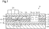
- Fig. 1 is a cross-sectional view showing one embodiment of an electronic device.
- the electronic device 10 of the present embodiment is, for example, an in-vehicle inverter device.
- the electronic device 10 includes a heat dissipation member 20, a power element 11a, a first metal plate 11 serving as a first conductive layer, two control elements 12a and 12b, and a second metal plate 12 serving as a second conductive layer.
- the power element 11a is electrically coupled to the first metal plate 11, and the control elements 12a and 12b are electrically coupled to the second metal plate 12.
- the power element 11 a is a metal-oxide-semiconductor field-effect transistor (MOSFET) and bare chip-mounted on the first metal plate 11.
- MOSFET metal-oxide-semiconductor field-effect transistor
- Each of the control elements 12a and 12b is, for example, a chip resistor or a capacitor.
- the heat dissipation member 20 is, for example, an aluminum housing including a coolant passage through which coolant flows.
- the first metal plate 11 and the second metal plate 12 are flat copper plates.
- the thickness H1 of the first metal plate 11 is greater than the thickness H2 of the second metal plate 12. Thus, a larger current flows to the first metal plate 11 than the second metal plate 12.
- the electronic device 10 includes a resin layer 13 located between the first metal plate 11 and the second metal plate 12.
- the power element 11 a is embedded in the resin layer 13.
- the resin layer 13 is formed from an epoxy resin including fillers that have a good thermal conductivity such as glass fiber.
- the first metal plate 11, the resin layer 13, and the second metal plate 12 are stacked on the heat dissipation member 20 in this order from the ones closer to the heat dissipation member 20. Thus, the first metal plate 11 is located closer to the heat dissipation member 20 than the second metal plate 12.
- the power element 11 a partially overlaps one of the control elements 12a in the direction in which the first metal plate 11, the resin layer 13, and the second metal plate 12 are stacked (hereinafter referred to as "stacking direction").
- the power element 11a is arranged between the first metal plate 11 and the resin layer 13 and embedded in the resin layer 13.
- a high thermal conduction insulative layer 14 is arranged between the heat dissipation member 20 and the first metal plate 11.
- the high thermal conduction insulative layer 14 is formed from an epoxy resin including fillers having a good thermal conductivity such as glass fiber.
- the amount of the fillers mixed with the epoxy resin that forms the high thermal conduction insulative layer 14 is greater than the amount of the fillers mixed in the epoxy resin that forms the resin layer 13.
- the high thermal conduction insulative layer 14 has a higher thermal conductivity than the resin layer 13.
- the power element 11a is electrically connected to the second metal plate 12 by two plate-shaped conductive members 15.
- Each flat conductive member 15 extends through the resin layer 13 in a vertical direction to a plane 111 a of the power element 11a that opposes the second metal plate 12.
- each conductive member 15 is arranged so that a thickness-wise direction of each conductive member 15 corresponds to a direction extending along the plane 111a of the power element 11a.
- the conductive members 15 form a path for the current flowing between the power element 11a and the control elements 12a and 12b.
- a switching operation of the power element 11a is performed when current flows between the control elements 12a and 12b and the power element 11a through the second metal plate 12 and the conductive members 15.
- the control elements 12a and 12b control the switching operation of the power element 11a.
- the electronic device 10 includes a third metal plate 16 having heat generating elements 16a that generate a smaller amount of heat than the control elements 12a and 12b.
- the third metal plate 16 is a flat copper plate.
- the third metal plate 16 and the first metal plate 11 are located at opposite sides of the second metal plate 12.
- An insulative layer 17 is arranged between the second metal plate 12 and the third metal plate 16. That is, the third metal plate 16 is arranged on the insulative layer 17.
- the insulative layer 17 is formed from an epoxy resin including fillers having a good thermal conductivity such as glass fiber.
- the thermal conductivity of the resin layer 13 is equal to that of the insulative layer 17.
- the control elements 12a and 12b are located between the second metal plate 12 and the insulative layer 17 and embedded in the insulative layer 17.
- the electronic device 10 includes a through hole 18 extending in the stacking direction through the third metal plate 16, the insulative layer 17, the second metal plate 12, and the resin layer 13.
- the through hole 18 accommodates an induction device 19 (for example, reactor) that is mounted on the first metal plate 11.
- the induction device 19 includes a coil 19a (shown by broken line in Fig. 1 ) that is electrically coupled to the first metal plate 11 and a core 19b (shown by broken line in Fig. 1 ) that is thermally coupled to the first metal plate 11.
- the induction device 19 does not extend beyond an upper surface of the third metal plate 16 (surface of third metal plate 16 located at side opposite to insulative layer 17).
- the power element 11a generates a greater amount of heat than the control elements 12a and 12b.
- the first metal plate 11 is located closer to the heat dissipation member 20 than the second metal plate 12.
- the heat dissipation member 20 gives priority to the dissipation of the heat generated from the power element 11 a over the dissipation of the heat generated from the control elements 12a and 12b.
- the high thermal conduction insulative layer 14 has a higher thermal conductivity than the resin layer 13. Thus, the heat generated from the power element 11a is transmitted more easily to the high thermal conduction insulative layer 14 than the resin layer 13.
- the heat generated from the power element 11a is transmitted through the first metal plate 11 and the high thermal conduction insulative layer 14 to the heat dissipation member 20 and dissipated from the heat dissipation member 20. Further, the heat generated from the coil 19a and the core 19b of the induction device 19 is transmitted through the first metal plate 11 and the high thermal conduction insulative layer 14 to the heat dissipation member 20 and dissipated from the heat dissipation member 20.
- the power element 11a does not have to overlap the control element 12a in the stacking direction.
- the shape of the conductive member 15 is not particularly limited.
- the conductive member 15 may be pin-shaped.
- the power element 11a may be electrically connected to the second metal plate 12 by a through hole.
- an insulative layer having the same thermal conductivity as the resin layer 13 may be arranged between the heat dissipation member 20 and the first metal plate 11.
- the high thermal conduction insulative layer 14 may be formed from a ceramic.
- the high thermal conduction insulative layer 14 may be omitted. Further, the first metal plate 11 may be bonded to the heat dissipation member 20.
- the numbers of the power element 11a and the control elements 12a and 12b are not particularly limited.
- the thickness H1 of the first metal plate 11 may be equal to the thickness H2 of the second metal plate 12.
- a metal plate may be arranged between the high thermal conduction insulative layer 14 and the heat dissipation member 20.
- an additional metal plate may be arranged between the third metal plate 16 and the insulative layer 17.
- an insulative layer that insulates the third metal plate 16 from the additional metal plate needs to be added.
- the heat dissipation member 20 may be, for example, a housing into which air flows to perform cooling.
- the electronic device 10 does not have to be an in-vehicle device.
- the present invention is not limited to the inverter device and may be applied to a DC-DC converter device.
Landscapes
- Engineering & Computer Science (AREA)
- Microelectronics & Electronic Packaging (AREA)
- Physics & Mathematics (AREA)
- Thermal Sciences (AREA)
- Power Engineering (AREA)
- Manufacturing & Machinery (AREA)
- Cooling Or The Like Of Semiconductors Or Solid State Devices (AREA)
- Inverter Devices (AREA)
- Ceramic Engineering (AREA)
- Production Of Multi-Layered Print Wiring Board (AREA)
- Cooling Or The Like Of Electrical Apparatus (AREA)
- Structures For Mounting Electric Components On Printed Circuit Boards (AREA)
- Structure Of Printed Boards (AREA)
Abstract
Description
- The present invention relates to an electronic device.
- Patent document 1 discloses a typical inverter device that is installed in a vehicle. The inverter device is an electronic device that converts direct current voltage into alternating current voltage. The inverter device includes a first metal plate (first conductive layer), on which a power element is mounted, and a second metal plate (second conductive layer), on which a control element is mounted. The control element controls a switching operation of the power element.
- Patent Document 1: Japanese Laid-Open Patent Publication No.
2010-73767 - The power element generates a greater amount of heat than the control element. Thus, it is desired that the power element be efficiently cooled. Further, in such an electronic device, for example, when the first metal plate and the second metal plate are arranged next to each other on the same plane, the planar size of the electronic device increases. In such a case, the limited available space in the vehicle makes it difficult for the electronic device to be installed in the vehicle.
- It is an object of the present invention to provide an electronic device that efficiently cools a power element and reduces the planar size of the electronic device.
- An electronic device that solves the above problem includes a heat dissipation member, a power element that is thermally coupled to the heat dissipation member, a first conductive layer to which the power element is electrically coupled, a control element that controls a switching operation of the power element, a second conductive layer to which the control element is electrically coupled, and a resin layer arranged between the first conductive layer and the second conductive layer. The power element is embedded in the resin layer. The first conductive layer, the resin layer, and the second conductive layer are stacked on the heat dissipation member in this order from the ones closer to the heat dissipation member.
-
Fig. 1 is a cross-sectional view showing one embodiment of an electronic device. - One embodiment of an
electronic device 10 will now be described with reference toFig. 1 . Theelectronic device 10 of the present embodiment is, for example, an in-vehicle inverter device. - As shown in
Fig. 1 , theelectronic device 10 includes aheat dissipation member 20, a power element 11a, afirst metal plate 11 serving as a first conductive layer, twocontrol elements second metal plate 12 serving as a second conductive layer. The power element 11a is electrically coupled to thefirst metal plate 11, and thecontrol elements second metal plate 12. The power element 11 a is a metal-oxide-semiconductor field-effect transistor (MOSFET) and bare chip-mounted on thefirst metal plate 11. Each of thecontrol elements heat dissipation member 20 is, for example, an aluminum housing including a coolant passage through which coolant flows. Thefirst metal plate 11 and thesecond metal plate 12 are flat copper plates. The thickness H1 of thefirst metal plate 11 is greater than the thickness H2 of thesecond metal plate 12. Thus, a larger current flows to thefirst metal plate 11 than thesecond metal plate 12. - The
electronic device 10 includes aresin layer 13 located between thefirst metal plate 11 and thesecond metal plate 12. The power element 11 a is embedded in theresin layer 13. Theresin layer 13 is formed from an epoxy resin including fillers that have a good thermal conductivity such as glass fiber. Thefirst metal plate 11, theresin layer 13, and thesecond metal plate 12 are stacked on theheat dissipation member 20 in this order from the ones closer to theheat dissipation member 20. Thus, thefirst metal plate 11 is located closer to theheat dissipation member 20 than thesecond metal plate 12. The power element 11 a partially overlaps one of thecontrol elements 12a in the direction in which thefirst metal plate 11, theresin layer 13, and thesecond metal plate 12 are stacked (hereinafter referred to as "stacking direction"). The power element 11a is arranged between thefirst metal plate 11 and theresin layer 13 and embedded in theresin layer 13. - A high thermal conduction
insulative layer 14 is arranged between theheat dissipation member 20 and thefirst metal plate 11. The high thermal conductioninsulative layer 14 is formed from an epoxy resin including fillers having a good thermal conductivity such as glass fiber. The amount of the fillers mixed with the epoxy resin that forms the high thermal conductioninsulative layer 14 is greater than the amount of the fillers mixed in the epoxy resin that forms theresin layer 13. Thus, the high thermal conductioninsulative layer 14 has a higher thermal conductivity than theresin layer 13. - The power element 11a is electrically connected to the
second metal plate 12 by two plate-shaped conductive members 15. Each flat conductive member 15 extends through theresin layer 13 in a vertical direction to a plane 111 a of the power element 11a that opposes thesecond metal plate 12. Thus, each conductive member 15 is arranged so that a thickness-wise direction of each conductive member 15 corresponds to a direction extending along the plane 111a of the power element 11a. The conductive members 15 form a path for the current flowing between the power element 11a and thecontrol elements control elements second metal plate 12 and the conductive members 15. Thus, thecontrol elements - The
electronic device 10 includes athird metal plate 16 having heat generating elements 16a that generate a smaller amount of heat than thecontrol elements third metal plate 16 is a flat copper plate. Thethird metal plate 16 and thefirst metal plate 11 are located at opposite sides of thesecond metal plate 12. Aninsulative layer 17 is arranged between thesecond metal plate 12 and thethird metal plate 16. That is, thethird metal plate 16 is arranged on theinsulative layer 17. Theinsulative layer 17 is formed from an epoxy resin including fillers having a good thermal conductivity such as glass fiber. The thermal conductivity of theresin layer 13 is equal to that of theinsulative layer 17. Thecontrol elements second metal plate 12 and theinsulative layer 17 and embedded in theinsulative layer 17. - The
electronic device 10 includes a throughhole 18 extending in the stacking direction through thethird metal plate 16, theinsulative layer 17, thesecond metal plate 12, and theresin layer 13. The throughhole 18 accommodates an induction device 19 (for example, reactor) that is mounted on thefirst metal plate 11. Theinduction device 19 includes acoil 19a (shown by broken line inFig. 1 ) that is electrically coupled to thefirst metal plate 11 and acore 19b (shown by broken line inFig. 1 ) that is thermally coupled to thefirst metal plate 11. Theinduction device 19 does not extend beyond an upper surface of the third metal plate 16 (surface ofthird metal plate 16 located at side opposite to insulative layer 17). - The operation of the present embodiment will now be described.
- The power element 11a generates a greater amount of heat than the
control elements first metal plate 11 is located closer to theheat dissipation member 20 than thesecond metal plate 12. Thus, theheat dissipation member 20 gives priority to the dissipation of the heat generated from the power element 11 a over the dissipation of the heat generated from thecontrol elements conduction insulative layer 14 has a higher thermal conductivity than theresin layer 13. Thus, the heat generated from the power element 11a is transmitted more easily to the high thermalconduction insulative layer 14 than theresin layer 13. As a result, the heat generated from the power element 11a is transmitted through thefirst metal plate 11 and the high thermalconduction insulative layer 14 to theheat dissipation member 20 and dissipated from theheat dissipation member 20. Further, the heat generated from thecoil 19a and the core 19b of theinduction device 19 is transmitted through thefirst metal plate 11 and the high thermalconduction insulative layer 14 to theheat dissipation member 20 and dissipated from theheat dissipation member 20. - The above embodiment has the advantages described below.
- (1) The
first metal plate 11, theresin layer 13, and thesecond metal plate 12 are stacked on theheat dissipation member 20 in this order from the ones closer to theheat dissipation member 20. Thefirst metal plate 11 is located closer to theheat dissipation member 20 than thesecond metal plate 12. Thus, theheat dissipation member 20 gives priority to the dissipation of the heat generated from the power element 11 a over the dissipation of the heat generated from thecontrol elements first metal plate 11, theresin layer 13, and thesecond metal plate 12 are stacked on theheat dissipation member 20. Thus, the power element 11 a is cooled more efficiently and the planar size of theelectronic device 10 is reduced as compared to when thefirst metal plate 11 and thesecond metal plate 12 are arranged next to each other on the same plane. - (2) The high thermal
conduction insulative layer 14 having a higher thermal conductivity than theresin layer 13 is located between theheat dissipation member 20 and thefirst metal plate 11. Thus, even in a structure in which theheat dissipation member 20 needs to be insulated from thefirst metal plate 11, the high thermalconduction insulative layer 14 located between theheat dissipation member 20 and thefirst metal plate 11 has a higher thermal conductivity than theresin layer 13. Accordingly, the heat transmitted from the power element 11a is transmitted to the high thermalconduction insulative layer 14 more easily than theresin layer 13. The heat transmitted to the high thermalconduction insulative layer 14 is further transmitted to theheat dissipation member 20 and dissipated from theheat dissipation member 20. Thus, even in a structure in which theheat dissipation member 20 needs to be insulated from thefirst metal plate 11, the power element 11a can be efficiently cooled. - (3) The power element 11a is connected to the
second metal plate 12 by the conductive members 15. The conductive members 15 extend through theresin layer 13 in the vertical direction to the plane of the power element 11a that opposes thesecond metal plate 12. This reduces the planar size of theelectronic device 10 as compared to when arranging the power element 11a and thesecond metal plate 12 next to each other on the same plane and connecting the power element 11a and thesecond metal plate 12 through wire bonding. - (4) The conductive members 15 are plate-shaped. Thus, as compared to when the power element 11a is electrically connected to the
second metal plate 12 by a through hole, the power element 11a and thesecond metal plate 12 are electrically connected in a further favorable manner. - (5) The power element 11a overlaps the
control element 12a in the stacking direction. This reduces the planar size of theelectronic device 10 as compared to when the power element 11a does not overlap thecontrol element 12a in the stacking direction. - (6) The
coil 19a is electrically coupled to thefirst metal plate 11, and the core 19b is thermally coupled to thefirst metal plate 11. Thus, the heat generated from thecoil 19a and the core 19b is transmitted through thefirst metal plate 11 and the high thermalconduction insulative layer 14 to theheat dissipation member 20 and dissipated from theheat dissipation member 20. This allows for effective cooling of thecoil 19a and the core 19b that generate a large amount of heat. - (7) The power element 11a is a MOSFET and bare-chip mounted on the
first metal plate 11. This reduces the size of theelectronic device 10 as compared to when a packaged power element is mounted on thefirst metal plate 11. - (8) The thickness H1 of the
first metal plate 11 is greater than the thickness H2 of thesecond metal plate 12. This reduces the size of theelectronic device 10 in a plan view as compared to when the planar size of thefirst metal plate 11 is increased. - (9) The
induction device 19 is accommodated in the throughhole 18 and does not extend beyond the upper surface of thethird metal plate 16. This reduces the size of theelectronic device 10 as compared to when theinduction device 19 extends beyond the upper surface of thethird metal plate 16. - (10) The heat generated from the power element 11a is transmitted through the
first metal plate 11 and the high thermalconduction insulative layer 14 to theheat dissipation member 20 and dissipated from theheat dissipation member 20. This limits situations in which the heat generated from the power element 11a is transmitted through the conductive members 15 and thesecond metal plate 12 to thecontrol elements - The above embodiment may be modified as described below.
- In the embodiment, the power element 11a does not have to overlap the
control element 12a in the stacking direction. - In the embodiment, the shape of the conductive member 15 is not particularly limited. For example, the conductive member 15 may be pin-shaped.
- In the embodiment, the power element 11a may be electrically connected to the
second metal plate 12 by a through hole. - In the embodiment, an insulative layer having the same thermal conductivity as the
resin layer 13 may be arranged between theheat dissipation member 20 and thefirst metal plate 11. - In the embodiment, the high thermal
conduction insulative layer 14 may be formed from a ceramic. - In the embodiment, as long as the
heat dissipation member 20 does not have to be insulated from thefirst metal plate 11, the high thermalconduction insulative layer 14 may be omitted. Further, thefirst metal plate 11 may be bonded to theheat dissipation member 20. - In the embodiment, the numbers of the power element 11a and the
control elements - In the embodiment, the thickness H1 of the
first metal plate 11 may be equal to the thickness H2 of thesecond metal plate 12. - In the embodiment, a metal plate may be arranged between the high thermal
conduction insulative layer 14 and theheat dissipation member 20. - In the embodiment, an additional metal plate may be arranged between the
third metal plate 16 and theinsulative layer 17. In this case, an insulative layer that insulates thethird metal plate 16 from the additional metal plate needs to be added. - In the embodiment, the
heat dissipation member 20 may be, for example, a housing into which air flows to perform cooling. - In the embodiment, the
electronic device 10 does not have to be an in-vehicle device. In addition, the present invention is not limited to the inverter device and may be applied to a DC-DC converter device.
Claims (8)
- An electronic device comprising:a heat dissipation member;a power element that is thermally coupled to the heat dissipation member;a first conductive layer to which the power element is electrically coupled;a control element that controls a switching operation of the power element;a second conductive layer to which the control element is electrically coupled; anda resin layer arranged between the first conductive layer and the second conductive layer, wherein the power element is embedded in the resin layer, whereinthe first conductive layer, the resin layer, and the second conductive layer are stacked on the heat dissipation member in this order from the ones closer to the heat dissipation member.
- The electronic device according to claim 1, wherein a high thermal conduction insulative layer having a higher thermal conductivity than the resin layer is arranged between the heat dissipation member and the first conductive layer.
- The electronic device according to claim 1 or 2, further comprising conductive members that extend through the resin layer in a vertical direction to a plane of the power element opposing the second conductive layer in order to connect the power element to the second conductive layer.
- The electronic device according to claim 3, wherein the conductive members are plate-shaped.
- The electronic device according to any one of claims 1 to 4, wherein the power element overlaps the control element in a stacking direction in which the first conductive layer, the resin layer, and the second conductive layer are stacked.
- The electronic device according to any one of claims 1 to 5, wherein
the resin layer and the second conductive layer include a through hole,
the through hole accommodates a coil and a core, and
the coil is electrically coupled to the first conductive layer and the core is thermally coupled to the first conductive layer. - The electronic device according to any one of claims 1 to 6, wherein
the power element is a MOSFET, and
the power element is bare-chip mounted on the first conductive layer. - The electronic device according to any one of claims 1 to 7, wherein the first conductive layer has a thickness that is greater than that of the second conductive layer.
Applications Claiming Priority (2)
| Application Number | Priority Date | Filing Date | Title |
|---|---|---|---|
| JP2014240286A JP6048481B2 (en) | 2014-11-27 | 2014-11-27 | Electronics |
| PCT/JP2015/081250 WO2016084579A1 (en) | 2014-11-27 | 2015-11-06 | Electronic device |
Publications (3)
| Publication Number | Publication Date |
|---|---|
| EP3226287A1 true EP3226287A1 (en) | 2017-10-04 |
| EP3226287A4 EP3226287A4 (en) | 2018-08-01 |
| EP3226287B1 EP3226287B1 (en) | 2019-08-28 |
Family
ID=56074149
Family Applications (1)
| Application Number | Title | Priority Date | Filing Date |
|---|---|---|---|
| EP15863142.4A Active EP3226287B1 (en) | 2014-11-27 | 2015-11-06 | Electronic device |
Country Status (6)
| Country | Link |
|---|---|
| US (1) | US10085368B2 (en) |
| EP (1) | EP3226287B1 (en) |
| JP (1) | JP6048481B2 (en) |
| KR (1) | KR101930391B1 (en) |
| CN (1) | CN107004645B (en) |
| WO (1) | WO2016084579A1 (en) |
Families Citing this family (7)
| Publication number | Priority date | Publication date | Assignee | Title |
|---|---|---|---|---|
| JP6048481B2 (en) | 2014-11-27 | 2016-12-21 | 株式会社豊田自動織機 | Electronics |
| JP2018010887A (en) * | 2016-07-11 | 2018-01-18 | 株式会社豊田自動織機 | Component built-in type multilayer substrate |
| US20180177045A1 (en) | 2016-12-21 | 2018-06-21 | At&S Austria Technologie & Systemtechnik Aktiengesellschaft | Embedding Component in Component Carrier by Component Fixation Structure |
| US10403558B2 (en) * | 2017-08-23 | 2019-09-03 | Ford Global Technologies, Llc | Power module with multi-layer substrate |
| KR102147792B1 (en) * | 2018-03-30 | 2020-08-25 | 삼성전기주식회사 | Rigid-flexible substrate module |
| US10912204B2 (en) * | 2018-03-30 | 2021-02-02 | Samsung Electro-Mechanics Co., Ltd. | Electronic device and rigid-flexible substrate module |
| CN112738994B (en) * | 2020-11-24 | 2022-12-09 | 鹤山市世拓电子科技有限公司 | Printed circuit board with embedded power device |
Family Cites Families (24)
| Publication number | Priority date | Publication date | Assignee | Title |
|---|---|---|---|---|
| JP2950290B2 (en) | 1997-06-27 | 1999-09-20 | 日本電気株式会社 | High frequency integrated circuit device and method of manufacturing the same |
| JP3673417B2 (en) * | 1998-12-03 | 2005-07-20 | ローム株式会社 | Multilayer hybrid integrated circuit device structure and manufacturing method thereof |
| JP4421081B2 (en) * | 1999-06-09 | 2010-02-24 | パナソニック株式会社 | Power module and manufacturing method thereof |
| JP2003115664A (en) * | 2001-10-05 | 2003-04-18 | Matsushita Electric Ind Co Ltd | Voltage conversion module |
| US6597575B1 (en) * | 2002-01-04 | 2003-07-22 | Intel Corporation | Electronic packages having good reliability comprising low modulus thermal interface materials |
| US6945312B2 (en) * | 2002-12-20 | 2005-09-20 | Saint-Gobain Performance Plastics Corporation | Thermal interface material and methods for assembling and operating devices using such material |
| JP2004214258A (en) * | 2002-12-27 | 2004-07-29 | Renesas Technology Corp | Semiconductor module |
| JP2008042120A (en) | 2006-08-10 | 2008-02-21 | Matsushita Electric Ind Co Ltd | Thermally conductive substrate, manufacturing method thereof, and electronic device using the same |
| JP2009123953A (en) * | 2007-11-15 | 2009-06-04 | Omron Corp | Transfer mold type power module |
| US9147649B2 (en) | 2008-01-24 | 2015-09-29 | Infineon Technologies Ag | Multi-chip module |
| JP2008263210A (en) * | 2008-05-16 | 2008-10-30 | Mitsubishi Electric Corp | Power semiconductor device |
| JP2010073767A (en) * | 2008-09-17 | 2010-04-02 | Jtekt Corp | Multilayer circuit board |
| JP5227770B2 (en) * | 2008-10-03 | 2013-07-03 | 古河電気工業株式会社 | Electronic substrate |
| JP2010199505A (en) * | 2009-02-27 | 2010-09-09 | Hitachi Ltd | Electronic circuit device |
| US8358000B2 (en) * | 2009-03-13 | 2013-01-22 | General Electric Company | Double side cooled power module with power overlay |
| JP2011044452A (en) * | 2009-08-19 | 2011-03-03 | Denso Corp | Electronic device and method of manufacturing the same |
| US8822281B2 (en) | 2010-02-23 | 2014-09-02 | Stats Chippac, Ltd. | Semiconductor device and method of forming TMV and TSV in WLCSP using same carrier |
| JP5423874B2 (en) * | 2010-03-18 | 2014-02-19 | 日本電気株式会社 | Semiconductor element-embedded substrate and manufacturing method thereof |
| JP2011243870A (en) * | 2010-05-20 | 2011-12-01 | Denso Corp | Coil mounting board |
| JP2012190955A (en) * | 2011-03-10 | 2012-10-04 | Furukawa Electric Co Ltd:The | Injection molded substrate |
| US9320173B2 (en) * | 2012-02-24 | 2016-04-19 | Mitsubishi Electric Corporation | Semiconductor device having a bulge portion and manufacturing method therefor |
| JP5807646B2 (en) * | 2013-01-15 | 2015-11-10 | トヨタ自動車株式会社 | Reactor with cooler |
| US9209151B2 (en) * | 2013-09-26 | 2015-12-08 | General Electric Company | Embedded semiconductor device package and method of manufacturing thereof |
| JP6048481B2 (en) | 2014-11-27 | 2016-12-21 | 株式会社豊田自動織機 | Electronics |
-
2014
- 2014-11-27 JP JP2014240286A patent/JP6048481B2/en active Active
-
2015
- 2015-11-06 KR KR1020177017115A patent/KR101930391B1/en active Active
- 2015-11-06 US US15/528,603 patent/US10085368B2/en active Active
- 2015-11-06 WO PCT/JP2015/081250 patent/WO2016084579A1/en not_active Ceased
- 2015-11-06 EP EP15863142.4A patent/EP3226287B1/en active Active
- 2015-11-06 CN CN201580063717.3A patent/CN107004645B/en active Active
Also Published As
| Publication number | Publication date |
|---|---|
| KR101930391B1 (en) | 2018-12-18 |
| US10085368B2 (en) | 2018-09-25 |
| WO2016084579A1 (en) | 2016-06-02 |
| CN107004645B (en) | 2019-08-23 |
| EP3226287B1 (en) | 2019-08-28 |
| US20170280595A1 (en) | 2017-09-28 |
| KR20170088930A (en) | 2017-08-02 |
| CN107004645A (en) | 2017-08-01 |
| JP6048481B2 (en) | 2016-12-21 |
| JP2016103538A (en) | 2016-06-02 |
| EP3226287A4 (en) | 2018-08-01 |
Similar Documents
| Publication | Publication Date | Title |
|---|---|---|
| EP3226287B1 (en) | Electronic device | |
| JP6584652B2 (en) | Power circuit equipment | |
| US8729692B2 (en) | Power module package | |
| JP6315091B2 (en) | Cooler and fixing method of cooler | |
| US20150116945A1 (en) | Semiconductor device and method for manufacturing same | |
| US11350517B2 (en) | Circuit device and power conversion device | |
| JP7345621B2 (en) | Power conversion device and method for manufacturing the power conversion device | |
| EP3038152A1 (en) | Wiring board and semiconductor package including wiring board | |
| WO2017060944A1 (en) | Electronic control device | |
| CN114446643B (en) | Power conversion device | |
| WO2022215357A1 (en) | Semiconductor device | |
| WO2021235485A1 (en) | Power conversion apparatus and method for manufacturing power conversion apparatus | |
| JP6076277B2 (en) | Power converter | |
| JP2016101071A (en) | Semiconductor device | |
| JP6308275B2 (en) | Electronics | |
| US9893624B2 (en) | Power supply unit having heat dissipation structure | |
| JP2009188192A (en) | Circuit equipment | |
| JP2023115513A (en) | power converter | |
| JP2013207242A (en) | Heating element heat radiation device and manufacturing method of the same | |
| CN104752381A (en) | Semiconductor device | |
| JP2017073528A (en) | Power supply device and switching hub having the same |
Legal Events
| Date | Code | Title | Description |
|---|---|---|---|
| STAA | Information on the status of an ep patent application or granted ep patent |
Free format text: STATUS: THE INTERNATIONAL PUBLICATION HAS BEEN MADE |
|
| PUAI | Public reference made under article 153(3) epc to a published international application that has entered the european phase |
Free format text: ORIGINAL CODE: 0009012 |
|
| STAA | Information on the status of an ep patent application or granted ep patent |
Free format text: STATUS: REQUEST FOR EXAMINATION WAS MADE |
|
| 17P | Request for examination filed |
Effective date: 20170606 |
|
| AK | Designated contracting states |
Kind code of ref document: A1 Designated state(s): AL AT BE BG CH CY CZ DE DK EE ES FI FR GB GR HR HU IE IS IT LI LT LU LV MC MK MT NL NO PL PT RO RS SE SI SK SM TR |
|
| AX | Request for extension of the european patent |
Extension state: BA ME |
|
| DAV | Request for validation of the european patent (deleted) | ||
| DAX | Request for extension of the european patent (deleted) | ||
| A4 | Supplementary search report drawn up and despatched |
Effective date: 20180702 |
|
| RIC1 | Information provided on ipc code assigned before grant |
Ipc: H01L 23/29 20060101AFI20180625BHEP Ipc: H05K 7/20 20060101ALI20180625BHEP Ipc: H05K 1/18 20060101ALI20180625BHEP Ipc: H05K 1/02 20060101ALI20180625BHEP Ipc: H05K 3/46 20060101ALI20180625BHEP |
|
| GRAP | Despatch of communication of intention to grant a patent |
Free format text: ORIGINAL CODE: EPIDOSNIGR1 |
|
| STAA | Information on the status of an ep patent application or granted ep patent |
Free format text: STATUS: GRANT OF PATENT IS INTENDED |
|
| INTG | Intention to grant announced |
Effective date: 20190311 |
|
| GRAS | Grant fee paid |
Free format text: ORIGINAL CODE: EPIDOSNIGR3 |
|
| GRAA | (expected) grant |
Free format text: ORIGINAL CODE: 0009210 |
|
| STAA | Information on the status of an ep patent application or granted ep patent |
Free format text: STATUS: THE PATENT HAS BEEN GRANTED |
|
| AK | Designated contracting states |
Kind code of ref document: B1 Designated state(s): AL AT BE BG CH CY CZ DE DK EE ES FI FR GB GR HR HU IE IS IT LI LT LU LV MC MK MT NL NO PL PT RO RS SE SI SK SM TR |
|
| REG | Reference to a national code |
Ref country code: GB Ref legal event code: FG4D |
|
| REG | Reference to a national code |
Ref country code: CH Ref legal event code: EP |
|
| REG | Reference to a national code |
Ref country code: AT Ref legal event code: REF Ref document number: 1173460 Country of ref document: AT Kind code of ref document: T Effective date: 20190915 |
|
| REG | Reference to a national code |
Ref country code: IE Ref legal event code: FG4D |
|
| REG | Reference to a national code |
Ref country code: DE Ref legal event code: R096 Ref document number: 602015036940 Country of ref document: DE |
|
| REG | Reference to a national code |
Ref country code: NL Ref legal event code: MP Effective date: 20190828 |
|
| REG | Reference to a national code |
Ref country code: LT Ref legal event code: MG4D |
|
| PG25 | Lapsed in a contracting state [announced via postgrant information from national office to epo] |
Ref country code: BG Free format text: LAPSE BECAUSE OF FAILURE TO SUBMIT A TRANSLATION OF THE DESCRIPTION OR TO PAY THE FEE WITHIN THE PRESCRIBED TIME-LIMIT Effective date: 20191128 Ref country code: NO Free format text: LAPSE BECAUSE OF FAILURE TO SUBMIT A TRANSLATION OF THE DESCRIPTION OR TO PAY THE FEE WITHIN THE PRESCRIBED TIME-LIMIT Effective date: 20191128 Ref country code: SE Free format text: LAPSE BECAUSE OF FAILURE TO SUBMIT A TRANSLATION OF THE DESCRIPTION OR TO PAY THE FEE WITHIN THE PRESCRIBED TIME-LIMIT Effective date: 20190828 Ref country code: HR Free format text: LAPSE BECAUSE OF FAILURE TO SUBMIT A TRANSLATION OF THE DESCRIPTION OR TO PAY THE FEE WITHIN THE PRESCRIBED TIME-LIMIT Effective date: 20190828 Ref country code: NL Free format text: LAPSE BECAUSE OF FAILURE TO SUBMIT A TRANSLATION OF THE DESCRIPTION OR TO PAY THE FEE WITHIN THE PRESCRIBED TIME-LIMIT Effective date: 20190828 Ref country code: LT Free format text: LAPSE BECAUSE OF FAILURE TO SUBMIT A TRANSLATION OF THE DESCRIPTION OR TO PAY THE FEE WITHIN THE PRESCRIBED TIME-LIMIT Effective date: 20190828 Ref country code: PT Free format text: LAPSE BECAUSE OF FAILURE TO SUBMIT A TRANSLATION OF THE DESCRIPTION OR TO PAY THE FEE WITHIN THE PRESCRIBED TIME-LIMIT Effective date: 20191230 Ref country code: FI Free format text: LAPSE BECAUSE OF FAILURE TO SUBMIT A TRANSLATION OF THE DESCRIPTION OR TO PAY THE FEE WITHIN THE PRESCRIBED TIME-LIMIT Effective date: 20190828 |
|
| PG25 | Lapsed in a contracting state [announced via postgrant information from national office to epo] |
Ref country code: GR Free format text: LAPSE BECAUSE OF FAILURE TO SUBMIT A TRANSLATION OF THE DESCRIPTION OR TO PAY THE FEE WITHIN THE PRESCRIBED TIME-LIMIT Effective date: 20191129 Ref country code: IS Free format text: LAPSE BECAUSE OF FAILURE TO SUBMIT A TRANSLATION OF THE DESCRIPTION OR TO PAY THE FEE WITHIN THE PRESCRIBED TIME-LIMIT Effective date: 20191228 Ref country code: RS Free format text: LAPSE BECAUSE OF FAILURE TO SUBMIT A TRANSLATION OF THE DESCRIPTION OR TO PAY THE FEE WITHIN THE PRESCRIBED TIME-LIMIT Effective date: 20190828 Ref country code: AL Free format text: LAPSE BECAUSE OF FAILURE TO SUBMIT A TRANSLATION OF THE DESCRIPTION OR TO PAY THE FEE WITHIN THE PRESCRIBED TIME-LIMIT Effective date: 20190828 Ref country code: LV Free format text: LAPSE BECAUSE OF FAILURE TO SUBMIT A TRANSLATION OF THE DESCRIPTION OR TO PAY THE FEE WITHIN THE PRESCRIBED TIME-LIMIT Effective date: 20190828 |
|
| REG | Reference to a national code |
Ref country code: AT Ref legal event code: MK05 Ref document number: 1173460 Country of ref document: AT Kind code of ref document: T Effective date: 20190828 |
|
| PG25 | Lapsed in a contracting state [announced via postgrant information from national office to epo] |
Ref country code: TR Free format text: LAPSE BECAUSE OF FAILURE TO SUBMIT A TRANSLATION OF THE DESCRIPTION OR TO PAY THE FEE WITHIN THE PRESCRIBED TIME-LIMIT Effective date: 20190828 |
|
| PG25 | Lapsed in a contracting state [announced via postgrant information from national office to epo] |
Ref country code: RO Free format text: LAPSE BECAUSE OF FAILURE TO SUBMIT A TRANSLATION OF THE DESCRIPTION OR TO PAY THE FEE WITHIN THE PRESCRIBED TIME-LIMIT Effective date: 20190828 Ref country code: IT Free format text: LAPSE BECAUSE OF FAILURE TO SUBMIT A TRANSLATION OF THE DESCRIPTION OR TO PAY THE FEE WITHIN THE PRESCRIBED TIME-LIMIT Effective date: 20190828 Ref country code: DK Free format text: LAPSE BECAUSE OF FAILURE TO SUBMIT A TRANSLATION OF THE DESCRIPTION OR TO PAY THE FEE WITHIN THE PRESCRIBED TIME-LIMIT Effective date: 20190828 Ref country code: AT Free format text: LAPSE BECAUSE OF FAILURE TO SUBMIT A TRANSLATION OF THE DESCRIPTION OR TO PAY THE FEE WITHIN THE PRESCRIBED TIME-LIMIT Effective date: 20190828 Ref country code: EE Free format text: LAPSE BECAUSE OF FAILURE TO SUBMIT A TRANSLATION OF THE DESCRIPTION OR TO PAY THE FEE WITHIN THE PRESCRIBED TIME-LIMIT Effective date: 20190828 Ref country code: PL Free format text: LAPSE BECAUSE OF FAILURE TO SUBMIT A TRANSLATION OF THE DESCRIPTION OR TO PAY THE FEE WITHIN THE PRESCRIBED TIME-LIMIT Effective date: 20190828 |
|
| PG25 | Lapsed in a contracting state [announced via postgrant information from national office to epo] |
Ref country code: IS Free format text: LAPSE BECAUSE OF FAILURE TO SUBMIT A TRANSLATION OF THE DESCRIPTION OR TO PAY THE FEE WITHIN THE PRESCRIBED TIME-LIMIT Effective date: 20200224 Ref country code: SK Free format text: LAPSE BECAUSE OF FAILURE TO SUBMIT A TRANSLATION OF THE DESCRIPTION OR TO PAY THE FEE WITHIN THE PRESCRIBED TIME-LIMIT Effective date: 20190828 Ref country code: CZ Free format text: LAPSE BECAUSE OF FAILURE TO SUBMIT A TRANSLATION OF THE DESCRIPTION OR TO PAY THE FEE WITHIN THE PRESCRIBED TIME-LIMIT Effective date: 20190828 Ref country code: SM Free format text: LAPSE BECAUSE OF FAILURE TO SUBMIT A TRANSLATION OF THE DESCRIPTION OR TO PAY THE FEE WITHIN THE PRESCRIBED TIME-LIMIT Effective date: 20190828 |
|
| REG | Reference to a national code |
Ref country code: DE Ref legal event code: R097 Ref document number: 602015036940 Country of ref document: DE |
|
| REG | Reference to a national code |
Ref country code: CH Ref legal event code: PL |
|
| PLBE | No opposition filed within time limit |
Free format text: ORIGINAL CODE: 0009261 |
|
| STAA | Information on the status of an ep patent application or granted ep patent |
Free format text: STATUS: NO OPPOSITION FILED WITHIN TIME LIMIT |
|
| PG2D | Information on lapse in contracting state deleted |
Ref country code: IS |
|
| PG25 | Lapsed in a contracting state [announced via postgrant information from national office to epo] |
Ref country code: CH Free format text: LAPSE BECAUSE OF NON-PAYMENT OF DUE FEES Effective date: 20191130 Ref country code: LU Free format text: LAPSE BECAUSE OF NON-PAYMENT OF DUE FEES Effective date: 20191106 Ref country code: MC Free format text: LAPSE BECAUSE OF FAILURE TO SUBMIT A TRANSLATION OF THE DESCRIPTION OR TO PAY THE FEE WITHIN THE PRESCRIBED TIME-LIMIT Effective date: 20190828 Ref country code: LI Free format text: LAPSE BECAUSE OF NON-PAYMENT OF DUE FEES Effective date: 20191130 |
|
| 26N | No opposition filed |
Effective date: 20200603 |
|
| REG | Reference to a national code |
Ref country code: BE Ref legal event code: MM Effective date: 20191130 |
|
| PG25 | Lapsed in a contracting state [announced via postgrant information from national office to epo] |
Ref country code: SI Free format text: LAPSE BECAUSE OF FAILURE TO SUBMIT A TRANSLATION OF THE DESCRIPTION OR TO PAY THE FEE WITHIN THE PRESCRIBED TIME-LIMIT Effective date: 20190828 |
|
| GBPC | Gb: european patent ceased through non-payment of renewal fee |
Effective date: 20191128 |
|
| PG25 | Lapsed in a contracting state [announced via postgrant information from national office to epo] |
Ref country code: FR Free format text: LAPSE BECAUSE OF NON-PAYMENT OF DUE FEES Effective date: 20191130 Ref country code: ES Free format text: LAPSE BECAUSE OF FAILURE TO SUBMIT A TRANSLATION OF THE DESCRIPTION OR TO PAY THE FEE WITHIN THE PRESCRIBED TIME-LIMIT Effective date: 20190828 Ref country code: IE Free format text: LAPSE BECAUSE OF NON-PAYMENT OF DUE FEES Effective date: 20191106 Ref country code: GB Free format text: LAPSE BECAUSE OF NON-PAYMENT OF DUE FEES Effective date: 20191128 |
|
| PG25 | Lapsed in a contracting state [announced via postgrant information from national office to epo] |
Ref country code: BE Free format text: LAPSE BECAUSE OF NON-PAYMENT OF DUE FEES Effective date: 20191130 |
|
| PG25 | Lapsed in a contracting state [announced via postgrant information from national office to epo] |
Ref country code: CY Free format text: LAPSE BECAUSE OF FAILURE TO SUBMIT A TRANSLATION OF THE DESCRIPTION OR TO PAY THE FEE WITHIN THE PRESCRIBED TIME-LIMIT Effective date: 20190828 |
|
| PG25 | Lapsed in a contracting state [announced via postgrant information from national office to epo] |
Ref country code: HU Free format text: LAPSE BECAUSE OF FAILURE TO SUBMIT A TRANSLATION OF THE DESCRIPTION OR TO PAY THE FEE WITHIN THE PRESCRIBED TIME-LIMIT; INVALID AB INITIO Effective date: 20151106 Ref country code: MT Free format text: LAPSE BECAUSE OF FAILURE TO SUBMIT A TRANSLATION OF THE DESCRIPTION OR TO PAY THE FEE WITHIN THE PRESCRIBED TIME-LIMIT Effective date: 20190828 |
|
| PG25 | Lapsed in a contracting state [announced via postgrant information from national office to epo] |
Ref country code: MK Free format text: LAPSE BECAUSE OF FAILURE TO SUBMIT A TRANSLATION OF THE DESCRIPTION OR TO PAY THE FEE WITHIN THE PRESCRIBED TIME-LIMIT Effective date: 20190828 |
|
| P01 | Opt-out of the competence of the unified patent court (upc) registered |
Effective date: 20230519 |
|
| REG | Reference to a national code |
Ref country code: DE Ref legal event code: R084 Ref document number: 602015036940 Country of ref document: DE |
|
| REG | Reference to a national code |
Ref country code: DE Ref legal event code: R079 Ref document number: 602015036940 Country of ref document: DE Free format text: PREVIOUS MAIN CLASS: H01L0023290000 Ipc: H10W0074400000 |
|
| PGFP | Annual fee paid to national office [announced via postgrant information from national office to epo] |
Ref country code: DE Payment date: 20250930 Year of fee payment: 11 |