WO2021235485A1 - Power conversion apparatus and method for manufacturing power conversion apparatus - Google Patents
Power conversion apparatus and method for manufacturing power conversion apparatus Download PDFInfo
- Publication number
- WO2021235485A1 WO2021235485A1 PCT/JP2021/018982 JP2021018982W WO2021235485A1 WO 2021235485 A1 WO2021235485 A1 WO 2021235485A1 JP 2021018982 W JP2021018982 W JP 2021018982W WO 2021235485 A1 WO2021235485 A1 WO 2021235485A1
- Authority
- WO
- WIPO (PCT)
- Prior art keywords
- cooling body
- main surface
- printed circuit
- circuit board
- substrate
- Prior art date
Links
Images


Classifications
-
- H—ELECTRICITY
- H02—GENERATION; CONVERSION OR DISTRIBUTION OF ELECTRIC POWER
- H02M—APPARATUS FOR CONVERSION BETWEEN AC AND AC, BETWEEN AC AND DC, OR BETWEEN DC AND DC, AND FOR USE WITH MAINS OR SIMILAR POWER SUPPLY SYSTEMS; CONVERSION OF DC OR AC INPUT POWER INTO SURGE OUTPUT POWER; CONTROL OR REGULATION THEREOF
- H02M1/00—Details of apparatus for conversion
- H02M1/32—Means for protecting converters other than automatic disconnection
- H02M1/327—Means for protecting converters other than automatic disconnection against abnormal temperatures
-
- H—ELECTRICITY
- H02—GENERATION; CONVERSION OR DISTRIBUTION OF ELECTRIC POWER
- H02M—APPARATUS FOR CONVERSION BETWEEN AC AND AC, BETWEEN AC AND DC, OR BETWEEN DC AND DC, AND FOR USE WITH MAINS OR SIMILAR POWER SUPPLY SYSTEMS; CONVERSION OF DC OR AC INPUT POWER INTO SURGE OUTPUT POWER; CONTROL OR REGULATION THEREOF
- H02M3/00—Conversion of dc power input into dc power output
- H02M3/003—Constructional details, e.g. physical layout, assembly, wiring or busbar connections
-
- H—ELECTRICITY
- H02—GENERATION; CONVERSION OR DISTRIBUTION OF ELECTRIC POWER
- H02M—APPARATUS FOR CONVERSION BETWEEN AC AND AC, BETWEEN AC AND DC, OR BETWEEN DC AND DC, AND FOR USE WITH MAINS OR SIMILAR POWER SUPPLY SYSTEMS; CONVERSION OF DC OR AC INPUT POWER INTO SURGE OUTPUT POWER; CONTROL OR REGULATION THEREOF
- H02M3/00—Conversion of dc power input into dc power output
- H02M3/22—Conversion of dc power input into dc power output with intermediate conversion into ac
- H02M3/24—Conversion of dc power input into dc power output with intermediate conversion into ac by static converters
- H02M3/28—Conversion of dc power input into dc power output with intermediate conversion into ac by static converters using discharge tubes with control electrode or semiconductor devices with control electrode to produce the intermediate ac
- H02M3/285—Single converters with a plurality of output stages connected in parallel
-
- H—ELECTRICITY
- H02—GENERATION; CONVERSION OR DISTRIBUTION OF ELECTRIC POWER
- H02M—APPARATUS FOR CONVERSION BETWEEN AC AND AC, BETWEEN AC AND DC, OR BETWEEN DC AND DC, AND FOR USE WITH MAINS OR SIMILAR POWER SUPPLY SYSTEMS; CONVERSION OF DC OR AC INPUT POWER INTO SURGE OUTPUT POWER; CONTROL OR REGULATION THEREOF
- H02M3/00—Conversion of dc power input into dc power output
- H02M3/22—Conversion of dc power input into dc power output with intermediate conversion into ac
- H02M3/24—Conversion of dc power input into dc power output with intermediate conversion into ac by static converters
- H02M3/28—Conversion of dc power input into dc power output with intermediate conversion into ac by static converters using discharge tubes with control electrode or semiconductor devices with control electrode to produce the intermediate ac
- H02M3/325—Conversion of dc power input into dc power output with intermediate conversion into ac by static converters using discharge tubes with control electrode or semiconductor devices with control electrode to produce the intermediate ac using devices of a triode or a transistor type requiring continuous application of a control signal
- H02M3/335—Conversion of dc power input into dc power output with intermediate conversion into ac by static converters using discharge tubes with control electrode or semiconductor devices with control electrode to produce the intermediate ac using devices of a triode or a transistor type requiring continuous application of a control signal using semiconductor devices only
- H02M3/33569—Conversion of dc power input into dc power output with intermediate conversion into ac by static converters using discharge tubes with control electrode or semiconductor devices with control electrode to produce the intermediate ac using devices of a triode or a transistor type requiring continuous application of a control signal using semiconductor devices only having several active switching elements
- H02M3/33573—Full-bridge at primary side of an isolation transformer
-
- H—ELECTRICITY
- H05—ELECTRIC TECHNIQUES NOT OTHERWISE PROVIDED FOR
- H05K—PRINTED CIRCUITS; CASINGS OR CONSTRUCTIONAL DETAILS OF ELECTRIC APPARATUS; MANUFACTURE OF ASSEMBLAGES OF ELECTRICAL COMPONENTS
- H05K1/00—Printed circuits
- H05K1/02—Details
- H05K1/14—Structural association of two or more printed circuits
- H05K1/148—Arrangements of two or more hingeably connected rigid printed circuit boards, i.e. connected by flexible means
-
- H—ELECTRICITY
- H05—ELECTRIC TECHNIQUES NOT OTHERWISE PROVIDED FOR
- H05K—PRINTED CIRCUITS; CASINGS OR CONSTRUCTIONAL DETAILS OF ELECTRIC APPARATUS; MANUFACTURE OF ASSEMBLAGES OF ELECTRICAL COMPONENTS
- H05K1/00—Printed circuits
- H05K1/18—Printed circuits structurally associated with non-printed electric components
- H05K1/181—Printed circuits structurally associated with non-printed electric components associated with surface mounted components
-
- H—ELECTRICITY
- H05—ELECTRIC TECHNIQUES NOT OTHERWISE PROVIDED FOR
- H05K—PRINTED CIRCUITS; CASINGS OR CONSTRUCTIONAL DETAILS OF ELECTRIC APPARATUS; MANUFACTURE OF ASSEMBLAGES OF ELECTRICAL COMPONENTS
- H05K3/00—Apparatus or processes for manufacturing printed circuits
- H05K3/0058—Laminating printed circuit boards onto other substrates, e.g. metallic substrates
- H05K3/0061—Laminating printed circuit boards onto other substrates, e.g. metallic substrates onto a metallic substrate, e.g. a heat sink
-
- H—ELECTRICITY
- H05—ELECTRIC TECHNIQUES NOT OTHERWISE PROVIDED FOR
- H05K—PRINTED CIRCUITS; CASINGS OR CONSTRUCTIONAL DETAILS OF ELECTRIC APPARATUS; MANUFACTURE OF ASSEMBLAGES OF ELECTRICAL COMPONENTS
- H05K7/00—Constructional details common to different types of electric apparatus
- H05K7/20—Modifications to facilitate cooling, ventilating, or heating
- H05K7/2089—Modifications to facilitate cooling, ventilating, or heating for power electronics, e.g. for inverters for controlling motor
- H05K7/209—Heat transfer by conduction from internal heat source to heat radiating structure
-
- H—ELECTRICITY
- H05—ELECTRIC TECHNIQUES NOT OTHERWISE PROVIDED FOR
- H05K—PRINTED CIRCUITS; CASINGS OR CONSTRUCTIONAL DETAILS OF ELECTRIC APPARATUS; MANUFACTURE OF ASSEMBLAGES OF ELECTRICAL COMPONENTS
- H05K2201/00—Indexing scheme relating to printed circuits covered by H05K1/00
- H05K2201/04—Assemblies of printed circuits
- H05K2201/047—Box-like arrangements of PCBs
-
- H—ELECTRICITY
- H05—ELECTRIC TECHNIQUES NOT OTHERWISE PROVIDED FOR
- H05K—PRINTED CIRCUITS; CASINGS OR CONSTRUCTIONAL DETAILS OF ELECTRIC APPARATUS; MANUFACTURE OF ASSEMBLAGES OF ELECTRICAL COMPONENTS
- H05K3/00—Apparatus or processes for manufacturing printed circuits
- H05K3/36—Assembling printed circuits with other printed circuits
- H05K3/366—Assembling printed circuits with other printed circuits substantially perpendicularly to each other
Definitions
- the present disclosure relates to a power conversion device and a method for manufacturing the power conversion device.
- the power conversion device includes electronic parts such as switching elements, rectifying elements, and magnetic parts. These electronic components generate heat as the power converter operates. The heat generated by these electronic components is transferred to the cooling body through the heat dissipation path, and is dissipated from the cooling body. In this way, the temperature of these electronic components is suppressed below the permissible temperature of each electronic component.
- Patent Document 1 Japanese Patent No. 4231626 (Patent Document 1) describes an automobile motor drive device.
- the power conversion element which is a high heat generation component
- the bottom surface of the housing in which the power conversion element is arranged is integrated with the cooling body.
- the printed circuit board on which the control element is mounted is fixed to the plate-shaped substrate mounting portion formed inside the housing. The heat generated by the control element is transferred to the housing via the plate-shaped substrate mounting portion. Further, the printed circuit board is laminated on the power conversion element.
- a power conversion element which is a high heat generation component
- the power conversion device becomes large.
- the heat generated by the control element is transferred to the housing via the plate-shaped substrate stationary portion. Therefore, the heat dissipation path becomes long. As a result, heat dissipation is reduced.
- the electrical connection technique between the component and the printed circuit board is not described in detail. Therefore, for example, when two printed circuit boards are connected to each other by a screw and a terminal block for fixing the harness and the harness, the Joule heat generated in the screw and the terminal block raises the temperature of the power converter.
- the present disclosure has been made in view of the above problems, and an object thereof is to suppress an expansion of the bottom area of the power conversion device, improve heat dissipation, and increase the temperature of the power conversion device. It is an object of the present invention to provide a power conversion device that can be suppressed and a method for manufacturing the power conversion device.
- the power conversion device of the present disclosure includes an electronic component, a first board, a first cooling body, a second board, a second cooling body, and a first wiring member.
- Electronic components include first and second components.
- the first substrate has a first main surface on which the first component of an electronic component is mounted and a second main surface facing the first main surface.
- the first cooling body is thermally connected to the second main surface of the first substrate.
- the second substrate has a third main surface on which the second component of the electronic component is mounted and a fourth main surface facing the third main surface.
- the second cooling body is thermally connected to the fourth main surface of the second substrate.
- the first wiring member electrically connects the first board and the second board.
- the second cooling body extends from the second main surface of the first substrate toward the first main surface.
- the first wiring member is connected to the first main surface of the first substrate and the third main surface of the second substrate by either direct connection or soldering joint, respectively.
- the electronic components are mounted not only on the first board but also on the second board. Therefore, even when the number of electronic components that are high heat generating components increases, the expansion of the first cooling body can be suppressed by mounting the electronic components on the second substrate. Therefore, it is possible to suppress the expansion of the bottom area of the power conversion device. Further, by mounting the electronic component on the second substrate, it is possible to shorten the heat dissipation distance in which the heat generated by the electronic component mounted on the second substrate is transferred to the second cooling body. Therefore, the heat dissipation of the second substrate can be improved. Further, the first wiring member is connected to the first main surface of the first substrate and the third main surface of the second substrate by either direct connection or soldering joint, respectively.
- FIG. It is a circuit diagram of the power conversion apparatus which concerns on Embodiment 1.
- FIG. It is a perspective view schematically showing the structure of the power conversion apparatus which concerns on Embodiment 1.
- FIG. It is a perspective view schematically showing the structure of the 1st printed circuit board module of the power conversion apparatus which concerns on Embodiment 1.
- FIG. It is a perspective view schematically showing the structure of the 2nd printed circuit board module of the power conversion apparatus which concerns on Embodiment 1.
- FIG. It is a perspective view schematically showing the structure of the 3rd printed circuit board module of the power conversion apparatus which concerns on Embodiment 1.
- FIG. It is sectional drawing which shows typically the structure of the power conversion apparatus which concerns on Embodiment 1.
- FIG. 3 is a perspective view schematically showing a configuration of a power conversion device according to a modification 3 of the first embodiment.
- FIG. 3 is a perspective view schematically showing a configuration of a power conversion device according to a modification 4 of the first embodiment.
- FIG. 5 is a perspective view schematically showing a configuration of a power conversion device according to a modification 5 of the first embodiment.
- FIG. 5 is a perspective view schematically showing a configuration of a power conversion device according to a modification 6 of the first embodiment.
- It is a perspective view schematically showing the structure of the power conversion apparatus which concerns on Embodiment 2.
- FIG. It is a perspective view which shows typically the structure of the power conversion apparatus which concerns on the modification of Embodiment 2.
- It is a perspective view schematically showing the structure of the power conversion apparatus which concerns on Embodiment 3.
- FIG. It is a perspective view for demonstrating the electrical connection between the printed circuit board modules of the power conversion apparatus which concerns on Embodiment 3.
- FIG. It is a perspective view for demonstrating the electrical connection between the printed circuit board modules of the power conversion apparatus which concerns on the modification of Embodiment 3.
- FIG. It is sectional drawing which shows typically the structure of the power conversion apparatus which concerns on Embodiment 4.
- FIG. It is a perspective view for demonstrating the electrical connection between the printed circuit board modules of the power conversion apparatus which concerns on Embodiment 5.
- FIG. It is sectional drawing which shows typically the structure of the power conversion apparatus which concerns on Embodiment 6.
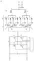
- FIG. 1 is an example of a circuit diagram of the power conversion device according to the first embodiment.
- the power conversion device shown in the circuit diagram of FIG. 1 is mounted on an electric vehicle, for example, and converts an input voltage of a lithium ion battery of DC100V to 300V into a voltage of DC12 to 15V and outputs the voltage to charge a lead storage battery. It is a DC-DC converter.
- the power conversion device shown in the circuit diagram of FIG. 1 includes an input capacitor 1, an inverter circuit unit 11 composed of four switching elements 2a, 2b, 2c and 2d, and a transformer unit 12 composed of transformers 3 and 4.
- the input is a rectifying circuit unit 13 composed of eight rectifying elements 5a, 5b, 5c, 5d, 5e, 5f, 5g, and 5h, a smoothing circuit unit 14 composed of reactors 6, 7, and a smoothing capacitor 8.
- a terminal 9, an output terminal 10, and a control circuit unit 15 are provided.
- each electronic component shown by a circuit symbol in FIG. 1 may have an arbitrary number of series configurations or parallel configurations.
- Each of the switching elements 2a, 2b, 2c, and 2d is a power semiconductor element such as a transistor, a MOSFET (Metal Oxide Semiconductor, Field Effect Transistor), and an IGBT (Insulated Gate Bipolar Transistor).
- the rectifying elements 5a, 5b, 5c, 5d, 5e, 5f, 5g, and 5h are power semiconductor elements such as diodes, MOSFETs, and thyristors.
- the power conversion device shown in the circuit diagram of FIG. 1 converts the DC voltage input from the input terminal 9 into an AC voltage by switching and controlling the inverter circuit unit 11 by the control circuit unit 15.
- the transformer unit 12 converts the AC voltage converted by the inverter circuit unit 11 into an arbitrary voltage according to the turns ratio of the transformers 3 and 4. Further, the transformers 3 and 4 electrically insulate between the input terminal 9 and the output terminal 10.
- the rectifier circuit unit 13 converts the AC voltage supplied from the transformers 3 and 4 into a DC voltage again.
- the smoothing circuit unit 14 smoothes the DC voltage converted by the rectifying circuit unit 13 to stabilize the output voltage.
- the wiring itself that electrically connects the high heat generation parts also generates a high heat generation amount. Therefore, when electrically connecting high heat-generating components with a circuit pattern formed on or inside the printed circuit board, it is necessary to dissipate the heat generated by the circuit pattern and keep the printed circuit board at an allowable temperature or lower.
- the permissible temperature of the printed circuit board is, for example, 100 ° C. or higher and 120 ° C. or lower.
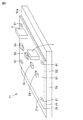
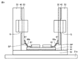
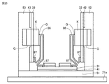
- FIG. 2 is a perspective view of the power conversion device 100 according to the first embodiment.
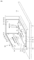
- FIG. 3 is a perspective view of the first printed circuit board module 71 included in the power conversion device 100.
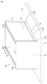
- FIG. 4 is a perspective view of the second printed circuit board module 72 included in the power conversion device 100.
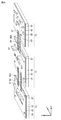
- FIG. 5 is a perspective view of the third printed circuit board module 73 included in the power conversion device 100. Note that the wiring member 86 and the joint portion 87, which will be described later, are not shown in FIGS. 2 to 5 for convenience of explanation.
- the power conversion device 100 includes an external cooling body 21, a first printed circuit board 31, a first insulating member 41, a first cooling body 51, and a first fixing member 61.
- the external cooling body 21 has a main surface 21a.
- the first printed circuit board (first board) 31 has a front surface (first main surface) S1 on which electronic components (first components) are mounted and a back surface (second main surface) S2 facing the first cooling body 51. have.
- the second main surface S2 faces the first main surface S1.
- the first insulating member 41 is arranged between the second main surface S2 of the first printed circuit board 31 and the first cooling body 51.
- the first cooling body 51 is thermally connected to the second main surface S2 of the first printed circuit board 31.
- the first cooling body 51 is thermally connected to the second main surface S2 of the first printed circuit board 31 via the first insulating member 41.
- the first cooling body 51 is thermally coupled to the external cooling body 21.
- the external cooling body 21 is thermally connected to the first cooling body 51.
- the first cooling body 51 is thermally connected to the second main surface S2 of the first printed circuit board 31.
- the first fixing member 61 is configured to fix the first printed circuit board 31 to the first cooling body 51.
- the second printed circuit board (second board) 32 has a front surface (third main surface) S3 on which electronic components (second components) are mounted and a back surface (fourth main surface) S4 facing the second cooling body 52. have.
- the fourth main surface S4 faces the third main surface S3.
- the second insulating member 42 is arranged between the fourth main surface S4 of the second printed circuit board 32 and the second cooling body 52.
- the second cooling body 52 is thermally connected to the fourth main surface S4 of the second printed circuit board 32.
- the second cooling body 52 is thermally connected to the fourth main surface S4 of the second printed circuit board 32 via the second insulating member 42.
- the second cooling body 52 is configured to extend vertically with the surface connected to the surface 51a of the first cooling body 51 facing the first printed circuit board 31 as the bottom surface.
- the second cooling body 52 extends from the second main surface S2 of the first printed circuit board 31 toward the first main surface S1.
- the second cooling body 52 is thermally connected to the first cooling body 51.
- the second fixing member 62 is configured to fix the second printed circuit board 32 to the second cooling body 52.
- the third printed circuit board (third board) 33 has a front surface (fifth main surface) S5 on which electronic components (third components) are mounted and a back surface (sixth main surface) S6 facing the third cooling body 53. have.
- the sixth main surface S6 faces the fifth main surface S5.
- the third insulating member 43 is arranged between the sixth main surface S6 of the third printed circuit board 33 and the third cooling body 53.
- the third cooling body 53 is thermally connected to the sixth main surface S6 of the third printed circuit board 33.
- the third cooling body 53 is thermally connected to the sixth main surface S6 of the third printed circuit board 33 via the third insulating member 43.
- the third cooling body 53 is configured to extend vertically with the surface connected to the surface 51a of the first cooling body 51 as the bottom surface.
- the third cooling body 53 extends from the second main surface S2 of the first printed circuit board 31 toward the first main surface S1.
- the third cooling body 53 is thermally connected to the first cooling body 51.
- the third fixing member 63 is configured to fix the third printed circuit board 33 to the third cooling body 53.
- Each of the second printed circuit board 32 and the third printed circuit board 33 extends in the direction from the second main surface S2 of the first printed circuit board 31 toward the first main surface S1.
- the second printed circuit board 32 and the third printed circuit board 33 are arranged so as to face each other.
- the first printed circuit board 31, the second printed circuit board, and the third printed circuit board 33 are configured inside the space composed of the cooling body.
- the second printed circuit board 32 and the third printed circuit board 33 are arranged so as to face each other, but they may be arranged so as to be adjacent to each other. At that time, the second printed circuit board 32 and the third printed circuit board 33 are thermally coupled.
- the vertical direction is a direction substantially perpendicular to the main surface 21a of the external cooling body 21.
- the first cooling body 51 constitutes the bottom surface of the support of the power conversion device 100.
- the second cooling body 52 and the third cooling body 53 form the side surface of the support of the power conversion device 100.
- the input power is connected to the first printed circuit board 31 from the upper opening of the second cooling body 52 or the third cooling body 53 by wiring such as a harness or a printed circuit board (not shown).
- the output power is output from the second printed circuit board 32 or the third printed circuit board 33.
- the second printed circuit board 32 or the third printed circuit board 33 for example, wiring of a harness or a printed circuit board for outputting output power is connected from an opening on the upper side of the housing (not shown).
- the control circuit unit 15 is arranged above the second cooling body 52 or the third cooling body 53 (not shown).
- the external cooling body 21 has a thermal conductivity of 1.0 W / (m ⁇ K) or more, preferably 10.0 W / (m ⁇ K) or more, and more preferably 100.0 W / (m ⁇ K) or more.
- the external cooling body 21 is formed of a metal material such as copper, iron, aluminum, an iron alloy, or an aluminum alloy, or a resin having a high thermal conductivity.
- the external cooling body 21 may be provided with a pipe for passing cooling water inside. Further, the external cooling body 21 may be provided with heat dissipation fins or the like in order to promote heat dissipation to the surrounding atmosphere.
- Each of the first printed circuit board 31, the second printed circuit board 32, and the third printed circuit board 33 may have a circuit pattern (not shown) formed on the surface or inside thereof.
- This circuit pattern has a thickness of 1 ⁇ m or more and 2000 ⁇ m or less.
- this circuit pattern is formed from a conductive material.
- This circuit pattern is formed from, for example, copper, nickel, gold, aluminum, silver, tin, etc. or alloys thereof.
- the materials constituting each of the first printed circuit board 31, the second printed circuit board 32, and the third printed circuit board 33 include, for example, glass fiber reinforced epoxy resin, phenol resin, polyphenylene sulfide (PPS), polyetheretherketone (PEEK), and the like. do it.
- each of the first printed circuit board 31, the second printed circuit board 32, and the third printed circuit board 33 may be made of a material generally having a low thermal conductivity. That is, each of the first printed circuit board 31, the second printed circuit board 32, and the third printed circuit board 33 may be a general-purpose printed circuit board. Further, each of the first printed circuit board 31, the second printed circuit board 32, and the third printed circuit board 33 may be made of ceramics such as aluminum oxide, aluminum nitride, and silicon carbide.
- Each of the first insulating member 41, the second insulating member 42, and the third insulating member 43 has electrical insulation. Further, each of the first insulating member 41, the second insulating member 42, and the third insulating member 43 may have elasticity. Further, each of the first insulating member 41, the second insulating member 42, and the third insulating member 43 may have a Young's modulus of 1 MPa or more and 100 MPa or less. Each of the first insulating member 41, the second insulating member 42, and the third insulating member 43 has a thermal conductivity of 0.1 W / (m ⁇ K) or more, preferably 1.0 W / (m ⁇ K) or more. ..
- Each of the first insulating member 41, the second insulating member 42 and the third insulating member 43 is made of, for example, a rubber material such as silicon or urethane, acrylonitrile butadiene styrene (ABS), polybutylene terephthalate (PBT), or polyphenylene sulfide (. It may be composed of a resin material such as PPS), a resin material such as phenol, a polymer material such as polyimide, a ceramic material such as alumina and aluminum nitride, and a phase change material containing silicon as a main raw material.
- a rubber material such as silicon or urethane, acrylonitrile butadiene styrene (ABS), polybutylene terephthalate (PBT), or polyphenylene sulfide (. It may be composed of a resin material such as PPS), a resin material such as phenol, a polymer material such as polyimide, a ceramic material such
- each of the first insulating member 41, the second insulating member 42, and the third insulating member 43 may be made of a material in which particles such as aluminum oxide, aluminum nitride, and boron nitride are mixed with a silicon resin.
- Each of the first cooling body 51, the second cooling body 52 and the third cooling body 53 is 1.0 W / (m ⁇ K) or more, preferably 10.0 W / (m ⁇ K) or more, more preferably 100. It has a thermal conductivity of 0 W / (m ⁇ K) or more.
- Each of the first cooling body 51, the second cooling body 52, and the third cooling body 53 is formed of a metal material such as copper, iron, aluminum, an iron alloy, or an aluminum alloy, or a resin having high thermal conductivity. ..
- the first cooling body 51, the second cooling body 52, and the third cooling body 53 are made of a plate-shaped aluminum alloy.
- each of the first cooling body 51, the second cooling body 52, and the third cooling body 53 may be electrically connected to another member so as to have the same potential as the ground. Further, each of the second cooling body 52 and the third cooling body 53 is connected to and fixed to the first cooling body 51 directly or via another member. Each of the second cooling body 52 and the third cooling body 53 is thermally connected to the first cooling body 51.
- a heat conductive grease, a heat conductive sheet, and a heat conductive adhesive are formed on the contact surface between the first cool body 51 and the second cool body 52 and the contact surface between the first cool body 51 and the third cool body 53.
- the heat conductive member (first heat conductive member) HC1 such as the above may be arranged.
- the heat conductive member (first heat conductive member) HC1 contains at least one of a heat conductive grease, a heat conductive sheet and a heat conductive adhesive.
- the first cooling body 51 is thermally connected to each of the second cooling body 52 and the third cooling body 53 via a heat conductive member (first heat conductive member) HC1.
- the first cooling body 51 may come into surface contact with the external cooling body 21.
- a heat conductive grease, a heat conductive sheet, a heat conductive adhesive, or the like is provided on the contact surface between the first cooling body 51 and the external cooling body 21.
- a heat conductive member may be arranged.
- the heat dissipation to the heat generated in the first printed circuit board module 71 is generated in the second printed circuit board module 72 and the third printed circuit board module 73. Higher than heat dissipation. Therefore, the electronic components arranged in the first printed circuit board module 71, the second printed circuit board module 72, and the third printed circuit board module 73 may be replaced, but the first printed circuit board module 71 generates particularly high heat generation electrons. It is preferable to arrange parts (high heat generation parts).
- each of the switching elements 2a, 2b, 2c, and 2d is a particularly heat-generating component
- each of the switching elements 2a, 2b, 2c, and 2d is attached to the first printed circuit board module 71. Deploy.
- the rectifying elements 5a, 5b, 5c, 5e, 5f, 5g, 5h or transformers 3 and 4 that generate less heat than the switching elements are arranged in the second printed circuit board module 72 and the third printed circuit board module 73.
- the first printed circuit board module 71 includes a first printed circuit board 31, a first insulating member 41, a first cooling body 51, a first fixing member 61, and an electronic component (first component). ) And.
- the electronic component (first component) is mounted on the first printed circuit board 31.
- the electronic component (first component) is each of the switching elements 2a, 2b, 2c, and 2d, which are particularly high heat generating components.
- the first insulating member 41 is provided between the first printed circuit board 31 and the first cooling body 51.
- the first insulating member 41 preferably comes into surface contact with the first printed circuit board 31 and the first cooling body 51.
- the first fixing member 61 fixes the first printed circuit board 31 to the first cooling body 51.
- the input capacitor 1 and the switching elements 2a, 2b, 2c, and 2d are mounted on the surface 31a of the first printed circuit board 31 opposite to the surface facing the first cooling body 51.
- An input terminal 9 (not shown) is mounted on the surface 31a.
- Other electronic components may be mounted on the surface 31a.
- other electronic components may be mounted on the surface of the first printed circuit board 31 facing the first cooling body 51.
- the surface of the first printed circuit board 31 facing the first cooling body 51 corresponds to the second main surface S2.
- the surface 31a of the first printed circuit board 31 opposite to the surface facing the first cooling body 51 corresponds to the first main surface S1.
- the second printed circuit board module 72 includes a second printed circuit board 32, a second insulating member 42, a second cooling body 52, a second fixing member 62, and an electronic component (second component). ) And.
- the electronic component (second component) is mounted on the second printed circuit board 32.
- the electronic components (second component) are transformers 3 and 4, which are particularly high heat generating components, and rectifying elements 5a, 5b, 5c, 5d, 5e, 5f, 5g, and 5h.
- the second insulating member 42 is provided between the fourth main surface S4 of the second printed circuit board 32 and the second cooling body 52.
- the second insulating member 42 preferably comes into surface contact with the second printed circuit board 32 and the second cooling body 52.
- the second fixing member 62 fixes the second printed circuit board 32 to the second cooling body 52.
- Rectifying elements 5a, 5b, 5c, 5d, 5e, 5f, 5g, 5h, and transformers 3 and 4 are mounted on the surface 32a of the second printed circuit board 32 opposite to the surface facing the second cooling body 52. Has been done. Other electronic components may be mounted on the surface 32a. Further, other electronic components may be mounted on the surface of the second printed circuit board 32 facing the second cooling body 52.
- the surface of the second printed circuit board 32 facing the second cooling body 52 corresponds to the fourth main surface S4.
- the surface 32a of the second printed circuit board 32 opposite to the surface facing the second cooling body 52 corresponds to the third main surface S3.
- the third printed circuit board module 73 includes a third printed circuit board 33, a third insulating member 43, a third cooling body 53, a third fixing member 63, and an electronic component (third component). ) And.
- the electronic component (third component) is mounted on the third printed circuit board 33.
- the electronic parts (third parts) are reactors 6 and 7, which are particularly high heat generating parts.
- the third insulating member 43 is provided between the third printed circuit board 33 and the third cooling body 53.
- the third insulating member 43 preferably comes into surface contact with the third printed circuit board 33 and the third cooling body 53.
- the third fixing member 63 fixes the third printed circuit board 33 to the third cooling body 53.
- the smoothing capacitor 8 and the reactors 6 and 7 are mounted on the surface 33a of the third printed circuit board 33 opposite to the surface facing the third cooling body 53. Further, an output terminal 10 (not shown) is mounted on the surface 33a. Further, other electronic components may be mounted on the surface 33a. Further, other electronic components may be mounted on the surface of the third printed circuit board 33 facing the third cooling body 53.
- the surface of the third printed circuit board 33 facing the third cooling body 53 corresponds to the sixth main surface S6.
- the surface 33a of the third printed circuit board 33 opposite to the surface facing the third cooling body 53 corresponds to the fifth main surface S5.
- the control circuit unit 15 shown in FIG. 1 may be mounted on any of the first printed circuit board 31, the second printed circuit board 32, and the third printed circuit board 33. Further, the control circuit unit 15 may be divided and mounted on at least two or more printed circuit boards among the first printed circuit board 31, the second printed circuit board 32, and the third printed circuit board 33.
- the power conversion device 100 includes an external cooling body 21, a first printed circuit board module 71, a second printed circuit board module 72, and a third printed circuit board module 73. ing.
- the wiring member 86 electrically connects between the first printed circuit board module 71 and the second printed circuit board module 72, and between the first printed circuit board module 71 and the third printed circuit board module 73.
- the wiring member 86 includes a first wiring member 86a and a second wiring member 86b.
- the first wiring member 86a electrically connects the first printed circuit board 31 of the first printed circuit board module 71 and the second printed circuit board 32 of the second printed circuit board module 72.
- the second wiring member 86b electrically connects the first printed circuit board 31 of the first printed circuit board module 71 and the third printed circuit board 33 of the third printed circuit board module 73.
- the first wiring member 86a is connected to the first main surface S1 of the first printed circuit board 31 and the third main surface S3 of the second printed circuit board 32 by either direct connection or soldering joint, respectively.
- the second wiring member 86b is joined to the first main surface S1 of the first printed circuit board 31 and the fifth main surface S5 of the third printed circuit board 33, respectively.
- bonding here refers to bonding by soldering, ultrasonic bonding, conductive adhesive, welding, or the like.
- a joint portion 87 is provided on the first main surface S1 of the first printed circuit board module 71.
- a joint portion 87 is provided on the third main surface S3 of the second printed circuit board module 72.
- a joint portion 87 is provided on the fifth main surface S5 of the third printed circuit board module 73.
- the wiring member 86 is electrically connected to the joint portion 87. A current of 0 to 300 A flows between the wiring member 86 and the joint portion 87.
- the wiring member 86 is formed of a conductive material.
- the wiring member 86 is formed of copper, nickel, gold, aluminum, silver, tin, or an alloy thereof.
- the shape of the wiring member 86 if the thickness is too thin, the width is too narrow, or the length is too long, the amount of heat generated when the wiring member 86 is energized becomes large. Therefore, the temperature rise of the wiring member 86 increases. Therefore, it is preferable that the shape of the wiring member 86 satisfies the following conditions.
- the wiring member 86 preferably has a thickness of 0.05 mm or more and less than 0.3 mm.
- the wiring member 86 preferably has a width of 3 mm or more and less than 50 mm.
- the wiring member 86 preferably has a length of 10 mm or more and less than 100 mm.
- the wiring member 86 preferably has a current density of 50 A / mm 2 or more and 100 A / mm 2 or less. Further, the aspect ratio of the wiring member 86 is preferably smaller than 1: 300.
- the wiring member 86 may have, for example, a thickness of 0.1 mm, a width of 10 mm, and a length of 50 mm, and may carry a current of 90 A.
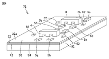
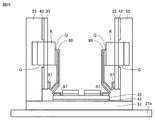
- FIG. 6 is a cross-sectional view schematically showing the configuration of the power conversion device 100. For convenience of explanation, hatching is not attached to FIG.
- FIG. 7 is a development view of the first printed circuit board module 71, the second printed circuit board module 72, and the third printed circuit board module 73 of the power conversion device 100.
- the thickness of the wiring member 86 is large, when the second printed circuit board module 72 and the third printed circuit board module 73 are bent as shown in FIG. 6 from the state shown in FIG. 7, the wiring member 86 and the joint portion 87 are bent. Cracks are likely to occur in the soldered part of the module.
- the thickness is 0. If it is less than mm, bending occurs in the Y-axis direction when the second printed circuit board module 72 and the third printed circuit board module 73 are bent perpendicularly to the first printed circuit board module 71 in the Z-axis direction. .. By deforming this bent portion in the Y-axis direction, it is possible to absorb the misalignment. Therefore, the thinner the thickness, the more the positional deviation in the Y-axis direction can be absorbed.
- the wiring member 86 is bent at a right angle and connected to the joint portion 87.
- the junction 87 is part of the circuit pattern.
- the wiring member 86 can be bent not only at a right angle but also at any angle from 0 degrees to 180 degrees.
- the second printed circuit board module 72 and the third printed circuit board module 73 can be bent in the Z-axis direction with respect to the first printed circuit board module 71. Therefore, each of the second printed circuit board module 72 and the third printed circuit board module 73 can be arranged perpendicularly to the external cooling body 21.
- the bottom area of the structure in which the first printed circuit board module 71, the second printed circuit board module 72, and the third printed circuit board module 73 are assembled is made smaller than that of the external cooling body 21, and this structure is made into the external cooling body 21. Can be implemented in.
- the direction parallel to the longitudinal direction of the wiring member 86 on the rectangular thin plate is defined as the X axis
- the direction perpendicular to the longitudinal direction is defined as the Y axis
- the direction perpendicular to the cooling surface is defined as the Z-axis direction.
- the position of the joint portion 87 may deviate from the design position in the Y-axis direction when the printed circuit board module is screwed to the cooling body.
- a misalignment in the Y-axis direction may occur. Further, in the state shown in FIG.
- the wiring member 86 can absorb the positional deviation in the Z-axis direction.
- the power conversion device 100 is manufactured through a preparation step S100, an assembly step S200, and a connection step S300.
- the electronic components including the first component, the second component, and the third component, the first printed circuit board 31, the second printed circuit board, the third printed circuit board 33, the first cooling body 51, and the second cooling body 52 ,
- the wiring member 86 is prepared.
- the printed circuit board may be divided from one board. In this case, the perforations formed on one substrate are cut by a router to be divided into each printed circuit board.
- each printed circuit board may be connected by a wiring member 86 via a joint portion 87.
- the perforations may be arranged so as not to overlap with the wiring member 86.
- the first printed circuit board module 71, the second printed circuit board module 72, and the third printed circuit board module 73 are assembled, respectively. Further, in the assembly step S200, each of the first printed circuit board module 71, the second printed circuit board module 72, and the third printed circuit board module 73 goes through an electronic component mounting step, a printed circuit board combination step, and a printed circuit board fixing step. Manufactured.
- the assembly process of the first printed circuit board module 71 will be described.
- the electronic component (first component) is mounted on the first main surface S1 of the first printed circuit board 31 by flow soldering, reflow soldering, or the like.
- the printed circuit board combination step the first cooling body 51, the first insulating member 41, and the first printed circuit board 31 on which the electronic component is mounted on the surface 31a are combined.
- the first cooling body 51 is thermally connected to the second main surface S2 facing the first main surface S1 of the first printed circuit board 31.
- the printed circuit board fixing step the first printed circuit board 31 is fixed to the first cooling body 51 by the first fixing member 61 via the first insulating member 41.
- the assembly process of the second printed circuit board module 72 will be described.
- the electronic component (second component) is mounted on the third main surface S3 of the second printed circuit board 32 by flow soldering, reflow soldering, or the like.
- the second cooling body 52, the second insulating member 42, and the second printed circuit board 32 on which the electronic component is mounted on the surface 32a are combined.
- the upper and lower cores are combined.
- the second cooling body 52 is thermally connected to the fourth main surface S4 facing the third main surface S3 of the second printed circuit board 32.
- the second printed circuit board 32 is fixed to the second cooling body 52 by the second fixing member 62 via the second insulating member 42.
- the assembly process of the third printed circuit board module 73 will be described.
- the electronic component (third component) is mounted on the fifth main surface S5 of the third printed circuit board 33 by flow soldering, reflow soldering, or the like.
- the third cooling body 53, the third insulating member 43, and the third printed circuit board 33 on which the electronic component is mounted on the surface 33a are combined.
- the upper and lower cores are combined.
- the third cooling body 53 is thermally connected to the sixth main surface S6 facing the fifth main surface S5 of the third printed circuit board 33.
- the third printed circuit board 33 is fixed to the third cooling body 53 by the third fixing member 63 via the third insulating member 43.
- the first wiring member 86a of the wiring member 86 electrically connects the first printed circuit board 31 and the second printed circuit board 32.
- the first wiring member 86a is connected to the first main surface S1 of the first printed circuit board 31 and the third main surface S3 of the second printed circuit board 32 by either direct connection or soldering joint, respectively.
- the first wiring member 86a is attached to the first printed circuit board 31. It may be electrically connected to the second printed circuit board 32.
- the first wiring member 86a is the first printed circuit board 31. And the second printed circuit board 32 may be electrically connected.
- the second wiring member 86b of the wiring member 86 electrically connects the first printed circuit board 31 and the third printed circuit board 33.
- the second wiring member 86b is connected to the first main surface S1 of the first printed circuit board 31 and the fifth main surface S5 of the third printed circuit board 33 by either direct connection or soldering joint, respectively.
- the first wiring member 86a is attached to the first printed circuit board 31. It may be electrically connected to the third printed circuit board 33.
- the first wiring member 86a is the first printed circuit board 31.
- the third printed circuit board 33 may be electrically connected.
- each of the second printed circuit board module 72 and the third printed circuit board module 73 is electrically connected to the first printed circuit board module 71 by a wiring member 86.
- the joint portion 87 is mounted on each of the first printed circuit board 31, the second printed circuit board 32, and the third printed circuit board 33.
- the wiring member 86 is electrically connected to the joint portion 87.
- each of the second printed circuit board module 72 and the third printed circuit board module 73 is electrically connected to the first printed circuit board module 71.
- the first printed circuit board 31 is connected to the second printed circuit board 32 and the third printed circuit board 33 by using the wiring member 86, but three or more boards are connected to one board. May be done.
- the joint portion 87 is a part of the circuit pattern, and is connected to the joint portion 87 by soldering without using a fastening member such as a screw and a terminal block. Further, the joint portion 87 may be connected to the joint portion 87 not only by soldering but also by welding, caulking, ultrasonic bonding or the like.
- each of the electronic component (second component) and the electronic component (third component) is fixed to the grooves G provided in each of the second printed circuit board 32 and the third printed circuit board 33.
- each of the second printed circuit board module 72 and the third printed circuit board module 73 is connected and fixed to the first printed circuit board module 71.
- the second cooling body 52 is arranged so as to extend in the direction from the second main surface S2 of the first printed circuit board 31 toward the first main surface S1.
- the third cooling body 53 is arranged so as to extend in the direction from the second main surface S2 of the first printed circuit board 31 toward the first main surface S1.
- connection step S300 the first cooling body 51 included in the first printed circuit board module 71, the second cooling body 52 included in the second printed circuit board module 72, and the third cooling body included in the third printed circuit board module 73.
- the 53 is connected and secured either directly or via other members.
- each of the second cooling body 52 and the third cooling body 53 is arranged so as to extend in the direction from the second main surface S2 of the first printed circuit board 31 toward the first main surface S1.
- the first cooling body 51 is thermally coupled to the external cooling body 21 by a method such as surface contact with the external cooling body 21.
- connection step S300 the second cooling body 52 and the third cooling body 53 are thermally connected to the first cooling body 51.
- the second cooling body 52 and the third cooling body 53 are assembled on the first cooling body 51 from the state of FIG. 7 as shown in FIG.
- the positions of the 87s and the positions of the joints 87 facing each other of the first printed circuit board 31 and the third printed circuit board 33 may be displaced. Even if the positions of the joints 87 are displaced, the connection can be maintained by the deformation of the wiring member 86.
- the electronic components are mounted not only on the first printed circuit board 31 but also on the second printed circuit board 32. Therefore, even when the number of electronic components that are high heat generation components increases, the expansion of the first cooling body 51 can be suppressed by mounting the electronic components on the second printed circuit board 32. Therefore, it is possible to suppress the expansion of the bottom area of the power conversion device 100. Further, by mounting the electronic component on the second printed circuit board 32, it is possible to shorten the heat dissipation distance in which the heat generated by the electronic component mounted on the second printed circuit board 32 is transferred to the second cooling body 52.
- the heat dissipation of the second printed circuit board 32 can be improved.
- the first wiring member 86a is connected to the first main surface S1 of the first printed circuit board 31 and the third main surface S3 of the second printed circuit board 32 by either direct connection or soldering joint, respectively. Therefore, since screws and terminal blocks are not used in the connection between the boards, the energization path is shortened by that amount, and the electric resistance is reduced. Therefore, the Joule heat generated in the screw and the terminal block is reduced, so that the temperature rise of the first wiring member 86a can be suppressed. Therefore, it is possible to suppress the temperature rise of the power conversion device 100. As a result, the power conversion device 100 according to the first embodiment can operate at a high output.
- the electronic component is also mounted on the third printed circuit board 33. Therefore, even when the number of electronic components that are high heat generation components increases, the expansion of the first cooling body 51 can be suppressed by mounting the electronic components on the third printed circuit board 33. Therefore, it is possible to suppress the expansion of the bottom area of the power conversion device 100. Further, by mounting the electronic component on the third printed circuit board 33, it is possible to shorten the heat dissipation path in which the heat generated by the electronic component mounted on the third printed circuit board 33 is transmitted to the third cooling body 53. Therefore, the heat dissipation of the third printed circuit board 33 can be improved.
- the second wiring member 86b is connected to the first main surface S1 of the first printed circuit board 31 and the fifth main surface S5 of the third printed circuit board 33 by either direct connection or soldering joint, respectively. Therefore, since screws and terminal blocks are not used in the connection between the boards, the energization path is shortened by that amount, and the electric resistance is reduced. Therefore, the Joule heat generated in the screw and the terminal block is reduced, so that the temperature rise of the second wiring member 86b can be suppressed. Therefore, it is possible to suppress the temperature rise of the power conversion device 100.
- the power conversion device 100 according to the first embodiment will be described in comparison with the comparative example.
- the terminal blocks installed at the joints 87 provided at the ends of the first printed circuit board 31 and the second printed circuit board 32 are connected by using screws and harnesses.
- the terminal block, screws, and the like installed at the joint portion 87 of the second printed circuit board 32 become the first printed circuit board 31. It interferes with the terminal block, screws, electronic parts, etc. installed at the end of the. Therefore, the first printed circuit board 31 and the second printed circuit board 32 must be mounted separately so that the components of the first printed circuit board 31 and the second printed circuit board 32 do not interfere with each other. Then, the volume and the bottom area of the power conversion device 100 become large.
- a thin ribbon-shaped copper plate is used as the wiring member 86 between the first printed circuit board 31 and the second printed circuit board 32 without using screws and terminal blocks.
- the joints 87 of the first printed circuit board 31 and the second printed circuit board 32 are connected to each other by soldering.
- the shape of the wiring member 86 has a large surface area in contact with air as compared with the circular wiring member having the same cross-sectional area. Therefore, it is possible to improve the heat dissipation of the power conversion device 100 with respect to the heat generated by the energization of the wiring member. Therefore, the current flowing through the power converter 100 can be increased. As a result, the power conversion device 100 according to the first embodiment can operate at a high output.
- the second printed circuit board 32 and the third printed circuit board 33 are arranged so as to face each other. Therefore, the power conversion device 100 can be miniaturized.
- the power conversion device 100 includes an external cooling body 21 thermally connected to the first cooling body 51.
- a heat dissipation path for radiating heat a first heat dissipation path for radiating heat to the external cooling body 21 can be formed via the first printed circuit board 31, the first insulating member 41, and the first cooling body 51.
- the heat radiated from the power conversion device 100 to the heat generated by the circuit pattern formed on the surface or the inside of the first printed circuit board 31 and the heat generated by the high heat generating component mounted on the first printed circuit board 31. Can improve sex.
- the power conversion device 100 according to the first embodiment can operate at a high output.
- the power conversion device 100 when the first insulating member 41 is brought into surface contact with the first printed circuit board 31 and the first cooling body 51, the area of the contact surface between the first insulating member 41 and the first printed circuit board 31 and the first insulation. Since the area of the contact surface between the member 41 and the first cooling body 51 can be widened, the contact thermal resistance of the contact surface between the first insulating member 41 and the first printed circuit board 31 and the first insulating member 41 and the first cooling body can be increased. The contact thermal resistance of the contact surface of 51 can be reduced, and the heat dissipation of the first heat dissipation path can be improved. As a result, the power conversion device 100 according to the first embodiment can operate at a high output.
- the second printed circuit board 32, the second insulating member 42, the second cooling body 52, and the first cooling body are used as heat dissipation paths to dissipate the heat generated by the 5e, 5f, 5g, 5h, and the transformers 3 and 4.
- a second heat dissipation path that dissipates heat to the external cooling body 21 can be formed via the 51.
- the second heat dissipation path does not include the plate-shaped substrate mounting portion as compared with the configuration described in Patent Document 1, the length of the heat dissipation path can be shortened and the heat dissipation can be improved. Therefore, the heat radiated from the power conversion device 100 to the heat generated by the circuit pattern formed on the surface or the inside of the second printed circuit board 32 and the heat generated by the high heat generating component mounted on the second printed circuit board 32. Can improve sex. As a result, the power conversion device 100 according to the first embodiment can operate at a high output.
- the power conversion device 100 when the second insulating member 42 is brought into surface contact with the second printed circuit board 32 and the second cooling body 52, the area of the contact surface between the second insulating member 42 and the second printed circuit board 32 and the second insulation Since the area of the contact surface between the member 42 and the second cooling body 52 can be widened, the contact thermal resistance of the contact surface between the second insulating member 42 and the second printed circuit board 32 and the second insulating member 42 and the second cooling body can be increased. The contact thermal resistance of the contact surface of 52 can be reduced, and the heat dissipation of the second heat dissipation path can be improved. As a result, the power conversion device 100 according to the first embodiment can operate at a high output.
- the power conversion device 100 when the lower surface of the core is in direct contact with the second cooling body 52, or the lower surface of the core is via a heat conductive member such as a heat conductive grease, a heat conductive sheet, or a heat conductive adhesive.
- a heat conductive member such as a heat conductive grease, a heat conductive sheet, or a heat conductive adhesive.
- the heat generated by the transformers 3 and 4 is transferred to the second cooling body. Since heat can be dissipated to the external cooling body 21 via the 52 and the first cooling body 51, the heat dissipation of the power conversion device 100 with respect to the heat generated by the transformers 3 and 4 can be improved. As a result, the power conversion device 100 according to the first embodiment can operate at a high output.
- the heat generated by the circuit pattern formed on the surface or the inside of the third printed circuit board 33 and the heat generated by the reactors 6 and 7, which are high heat generating components mounted on the third printed circuit board 33, are combined with each other.
- a heat dissipation path a third heat dissipation path that dissipates heat to the external cooling body 21 can be formed via the third printed circuit board 33, the third insulating member 43, the third cooling body 53, and the first cooling body 51. .. Since the third heat dissipation path does not include the plate-shaped substrate mounting portion as compared with the configuration described in Patent Document 1, the length of the heat dissipation path can be shortened and the heat dissipation can be improved.
- the heat radiated from the power conversion device 100 to the heat generated by the circuit pattern formed on the surface or the inside of the third printed circuit board 33 and the heat generated by the high heat generating component mounted on the third printed circuit board 33. Can improve sex.
- the power conversion device 100 according to the first embodiment can operate at a high output.
- the power conversion device 100 when the third insulating member 43 is brought into surface contact with the third printed circuit board 33 and the third cooling body 53, the area of the contact surface between the third insulating member 43 and the third printed circuit board 33 and the third insulation. Since the area of the contact surface between the member 43 and the third cooling body 53 can be widened, the contact thermal resistance of the contact surface between the third insulating member 43 and the third printed circuit board 33 and the third insulating member 43 and the third cooling body can be increased. The contact thermal resistance of the contact surface of 53 can be reduced, and the heat dissipation of the third heat dissipation path can be improved. As a result, the power conversion device 100 according to the first embodiment can operate at a high output.
- the power conversion device 100 when the lower surface of the core is in direct contact with the third cooling body 53, or the lower surface of the core is via a heat conductive member such as a heat conductive grease, a heat conductive sheet, or a heat conductive adhesive.
- a heat conductive member such as a heat conductive grease, a heat conductive sheet, or a heat conductive adhesive.
- the heat generated by the reactors 6 and 7 is transferred to the third cooling body. Since heat can be dissipated to the external cooling body 21 via the 53 and the first cooling body 51, the heat dissipation of the power conversion device 100 with respect to the heat generated by the reactors 6 and 7 can be improved. As a result, the power conversion device 100 according to the first embodiment can operate at a high output.
- the power conversion device 100 can operate at a high output.
- the thickness of the first cooling body 51 in the direction substantially perpendicular to the surface 31a of the first printed circuit board 31 is thin.
- the lengths of the first heat dissipation path, the second heat dissipation path, and the third heat dissipation path can be shortened, so that the heat dissipation property can be improved.
- the thickness of the second cooling body 52 in the direction substantially perpendicular to the surface 32a of the second printed circuit board 32 is increased.
- the thermal resistance of the second cooling body 52 included in the second heat dissipation path can be reduced, so that the heat dissipation can be improved.
- the thickness of the third cooling body 53 in the direction substantially perpendicular to the surface 33a of the third printed circuit board 33 is increased.
- the thermal resistance of the third cooling body 53 included in the third heat dissipation path can be reduced, so that the heat dissipation can be improved.
- the first cooling body 51 can be thermally connected to the first printed circuit board 31 via the first insulating member 41.
- the second cooling body 52 can be thermally connected to the second printed circuit board 32 via the second insulating member 42.
- the third cooling body 53 can be thermally connected to the third printed circuit board 33 via the third insulating member 43.
- the second cooling body 52 is thermally connected to the first cooling body 51
- the third cooling body 53 is thermally connected to the first cooling body 51. Has been done. Therefore, the heat generated by the electronic components mounted on the second printed circuit board 32 can be dissipated from the first cooling body 51 via the second cooling body 52, and the electronic components mounted on the third printed circuit board 33 can be dissipated. The heat generated in the above can be dissipated from the first cooling body 51 via the third cooling body 53.
- the first cooling body 51 is thermally connected to each of the second cooling body 52 and the third cooling body 53 via the first heat conductive member HC1. ing. Therefore, the heat transfer efficiency from the second cooling body 52 to the first cooling body 51 can be improved by the first heat conductive member HC1, and the heat transfer efficiency from the third cooling body 53 to the first cooling body 51 can be improved. Can be improved.
- the wiring member 86 has a thickness of 0.05 mm or more and less than 0.3 mm, and has a current density of 50 A / mm 2 or more and 100 / mm 2 or more. Therefore, the thin wiring member 86 can be energized with a large current.
- the manufacturing method of the power conversion device 100 includes a preparation step S100, an assembly step S200, and a connection step S300. Therefore, the first cooling body 51 constituting the bottom surface of the support, the second cooling body 52 and the third cooling body 53 forming the side surfaces of the support, the first insulating member 41, the second insulating member 42, and the third The work of arranging the insulating member 43 and fixing the first printed circuit board 31, the second printed circuit board 32, and the third printed circuit board 33, and the first printed circuit board module 71, the second printed circuit board module 72, and the third printed circuit board module 73. It is no longer necessary to perform the work of electrically connecting the spaces in a space that is roughly enclosed. As a result, it is not necessary to design the heat in consideration of the thickness variation of the first insulating member 41, the second insulating member 42, and the third insulating member 43 due to the poor workability.
- the second cooling body 52 is arranged so as to extend from the second main surface S2 of the first printed circuit board 31 toward the first main surface S1.
- the first wiring member 86a electrically connects the first printed circuit board 31 and the second printed circuit board 32.
- the first wiring member 86a is connected to the first main surface S1 of the first printed circuit board 31 and the third main surface S3 of the second printed circuit board 32 by either direct connection or soldering joint, respectively. Therefore, the power conversion device 100 can be miniaturized, the heat dissipation can be improved, and the temperature rise of the power conversion device 100 can be suppressed.
- the switching elements 2a, 2b, 2c, and 2d which are high heat generating components, are arranged in the first printed circuit board module 71.
- the high heat generation component can reduce the thermal resistance to the external cooling body. Therefore, the power conversion device 100 can be miniaturized, the heat dissipation can be improved, and the temperature rise of the power conversion device 100 can be suppressed.
- the third cooling body 53 is arranged so as to extend in the direction from the second main surface S2 of the first printed circuit board 31 toward the first main surface S1.
- the second wiring member 86b electrically connects the first printed circuit board 31 and the third printed circuit board 33.
- the second wiring member 86b is connected to the first main surface S1 of the first printed circuit board 31 and the fifth main surface S5 of the third printed circuit board 33 by either direct connection or soldering joint, respectively. Therefore, the power conversion device 100 can be miniaturized, the heat dissipation can be improved, and the temperature rise of the power conversion device 100 can be suppressed.
- the second cooling body 52 and the third cooling body 53 are thermally connected to the first cooling body 51. Therefore, the power conversion device 100 can be miniaturized, the heat dissipation can be improved, and the temperature rise of the power conversion device 100 can be suppressed.
- an electronic component (second component) and an electronic component (second component) are formed in the grooves G provided in each of the second printed circuit board 32 and the third printed circuit board 33.
- Each of the electronic components (third component) is fixed. Therefore, the power conversion device 100 can be miniaturized, the heat dissipation can be improved, and the temperature rise of the power conversion device 100 can be suppressed. Further, the electronic component can be securely fixed.
- the power conversion device 100 according to the modified example of the first embodiment will be described.
- the modified example of the first embodiment has the same configuration, operation, and effect as that of the first embodiment. Therefore, the same components as those in the first embodiment are designated by the same reference numerals, and the description thereof will not be repeated.
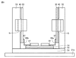
- FIG. 9 is a cross-sectional view showing a state after the first cooling body 51, the second cooling body 52, and the third cooling body 53 are assembled as shown in FIG. Note that hatching is not attached to FIG. 9 for convenience of explanation.
- the power conversion device 100 according to the first modification of the first embodiment basically has the same configuration as the power conversion device 100 according to the first embodiment.
- the power conversion device 100 according to the first modification of the first embodiment has a different shape of the wiring member 86 than the power conversion device 100 according to the first embodiment.
- the shape of the wiring member 86 is on a straight line.
- the wiring member 86 is preliminarily folded so that the wiring member 86 is bent a plurality of times.
- the wiring member 86 is configured in a bellows shape having a plurality of bent portions BP. That is, the wiring member 86 has a plurality of bent portions BP. Of the plurality of bent portions BP, the adjacent bent portion BPs are arranged so as to overlap each other.
- the effect of the power conversion device 100 according to the first modification of the first embodiment will be described.
- the wiring member 86 since the wiring member 86 has a plurality of bent portions BP, the wiring member 86 is miniaturized by being folded. Further, among the plurality of bent portions BP, the adjacent bent portion BPs are arranged so as to overlap each other. Therefore, when the wiring member 86 is bent, the mountain and the mountain of the bent wiring member 86 overlap each other, and the energization path of the wiring member 86 becomes short. As a result, the electric resistance of the wiring member 86 is further reduced, so that heat generation can be reduced. As a result, the power conversion device 100 according to the first modification of the first embodiment can operate at a high output.
- the power conversion device 100 according to the second modification of the first embodiment will be described with reference to FIGS. 10 and 11. Note that hatching is not attached to FIG. 11 for convenience of explanation.
- the power conversion device 100 according to the second modification of the first embodiment basically has the same configuration as the power conversion device 100 according to the first embodiment.
- the power conversion device 100 according to the second modification of the first embodiment has a different shape of the wiring member 86 than the power conversion device 100 according to the first embodiment.
- the wiring member 86 is preliminarily bent in an arch shape in the positive direction of the Z axis.
- the structure has a space in the lower center of the wiring member 86.
- the wiring member 86 has a shape bent so as to be adjacent to the joint portions 87 at both ends of the wiring member 86. Then, the component can be installed in the space at the lower center of the wiring member 86 that is bent in the positive direction of the Z axis.
- the center of the wiring member 86 bulges in an arc shape and has a shape facing the joint portion 87 of the wiring member 86, and the two bending portions CP provided on the wiring member 86 are close to each other.
- the bent portion CP of the wiring member 86 is provided so as to be adjacent to the end portions of the first printed circuit board 31, the second printed circuit board 32, and the third printed circuit board 33, and even if the bent portion CP of the wiring member 86 comes into contact with each other. good.
- the contact between the bent portions CP of the wiring member 86 shortens the energization path when the printed circuit board modules are brought close to each other.
- the wiring member 86 faces the joint portion 87 by the center of the wiring member 86 bulging in an arch shape.
- the contact between the two bent portions CP provided on the wiring member 86 shortens the energization path.
- the electric resistance of the wiring member 86 is reduced, so that heat generation can be reduced.
- the power conversion device 100 according to the second modification of the first embodiment can operate at a high output.
- the power conversion device 100 according to the third modification of the first embodiment basically has the same configuration as the power conversion device 100 according to the first embodiment.
- the power conversion device 100 according to the third modification of the first embodiment has a first cooling body 51, a second cooling body 52, and a third cooling body 53 as compared with the power conversion device 100 according to the first embodiment.
- the arrangement of is different.
- the first cooling body 51 is arranged so as to be sandwiched between the second cooling body 52 and the third cooling body 53.
- the power conversion device 100 according to the modified example 4 of the first embodiment will be described with reference to FIG.
- the power conversion device 100 according to the fourth modification of the first embodiment basically has the same configuration as the power conversion device 100 according to the first embodiment.
- the power conversion device 100 according to the fourth modification of the first embodiment has a different configuration of the first cooling body 51 and the external cooling body 21 than the power conversion device 100 according to the first embodiment.
- the first cooling body 51 is integrally formed with the external cooling body 21.
- the first cooling body 51 also serves as the external cooling body 21.
- the first cooling body 51 is thermally coupled to the external cooling body 21 by a method such as integrally forming with the external cooling body 21.
- the power conversion device 100 according to the modified example 5 of the first embodiment will be described with reference to FIG.
- the power conversion device 100 according to the fifth modification of the first embodiment basically has the same configuration as the power conversion device 100 according to the first embodiment.
- the power conversion device 100 according to the fifth modification of the first embodiment has a different arrangement of the second printed circuit board module 72 than the power conversion device 100 according to the first embodiment.
- the second printed circuit board module 72 and the third printed circuit board module 73 are arranged so as to be adjacent to each other.
- the second printed circuit board 32 and the third printed circuit board 33 are arranged so as to be adjacent to each other.
- the second printed circuit board 32 and the third printed circuit board 33 are arranged so as to be adjacent to each other. Therefore, the power conversion device 100 can be miniaturized.
- the power conversion device 100 according to the modification 6 of the first embodiment will be described with reference to FIG.
- the power conversion device 100 according to the sixth modification of the first embodiment basically has the same configuration as the power conversion device 100 according to the first embodiment.
- the power conversion device 100 according to the sixth modification of the first embodiment is different from the power conversion device 100 according to the first embodiment in that the third printed circuit board module 73 is not arranged.
- the power conversion device 100 according to the sixth modification of the first embodiment does not have the third printed circuit board module 73.
- Embodiment 2 the power conversion device 100 according to the second embodiment will be described with reference to FIG.
- the second embodiment has the same configuration, operation, and effect as the first embodiment, unless otherwise specified. Therefore, the same components as those in the first embodiment are designated by the same reference numerals, and the description thereof will not be repeated.
- the power conversion device 100 according to the second embodiment basically has the same configuration as the power conversion device 100 according to the first embodiment.
- the power conversion device 100 according to the second embodiment is different from the power conversion device 100 according to the first embodiment in that it includes a fourth cooling body 54 and a fifth cooling body 55.
- the fourth cooling body 54 is configured to extend vertically with the surface connected to the surface 51a of the first cooling body 51 as the bottom surface.
- the fourth cooling body 54 extends from the second main surface S2 of the first printed circuit board 31 toward the first main surface S1.
- the fifth cooling body 55 is configured to extend vertically with the surface connected to the surface 51a of the first cooling body 51 as the bottom surface.
- the fifth cooling body 55 extends from the second main surface S2 of the first printed circuit board 31 toward the first main surface S1.
- Each of the fourth cooling body 54 and the fifth cooling body 55 cools at least one of the first cooling body 51, the second cooling body 52, and the third cooling body 53 directly or via other members. Connected and secured to the body.
- Each of the fourth cooling body 54 and the fifth cooling body 55 is thermally connected to each of the first cooling body 51, the second cooling body 52, and the third cooling body 53.
- the fourth cooling body 54 is thermally connected to the first cooling body 51, the second cooling body 52, and the third cooling body 53.
- the fifth cooling body 55 is thermally connected to the first cooling body 51, the second cooling body 52, and the third cooling body 53.
- a heat conductive member such as a heat conductive adhesive (second heat conductive member) HC2 may be arranged.
- the heat conductive member (second heat conductive member) HC2 contains at least one of a heat conductive grease, a heat conductive sheet and a heat conductive adhesive.
- the fourth cooling body 54 is thermally connected to each of the first cooling body 51, the second cooling body 52, and the third cooling body 53 via a heat conductive member (second heat conductive member) HC2.
- the fifth cooling body 55 is thermally connected to each of the first cooling body 51, the second cooling body 52, and the third cooling body 53 via a heat conductive member (second heat conductive member) HC2.
- Each of the fourth cooling body 54 and the fifth cooling body 55 constitutes a side surface of the support of the power conversion device 100.
- the power conversion device 100 according to the second embodiment can obtain the same effect as the power conversion device 100 according to the first embodiment.
- the second printed circuit board 32, the second insulating member 42, the second cooling body 52, and the first cooling are used as heat dissipation paths to dissipate the heat generated by the 5e, 5f, 5g, 5h and the transformers 3 and 4.
- the first is heat dissipation to the external cooling body 21 via the second printed circuit board 32, the second insulating member 42, the second cooling body 52, the fourth cooling body 54, and the first cooling body 51. It is a route.
- the second is heat dissipation to the external cooling body 21 via the second printed circuit board 32, the second insulating member 42, the second cooling body 52, the fifth cooling body 55, and the first cooling body 51. It is a route.
- the following two heat dissipation paths are formed.
- the first is heat dissipation to the external cooling body 21 via the third printed circuit board 33, the third insulating member 43, the third cooling body 53, the fourth cooling body 54, and the first cooling body 51. It is a route.
- the second is heat dissipation to the external cooling body 21 via the third printed circuit board 33, the third insulating member 43, the third cooling body 53, the fifth cooling body 55, and the first cooling body 51. It is a route. Therefore, the heat radiated from the power conversion device 100 to the heat generated by the circuit pattern formed on the surface or the inside of the third printed circuit board 33 and the heat generated by the high heat generating component mounted on the third printed circuit board 33. It can enhance the sex. As a result, the power conversion device 100 according to the second embodiment can operate at a high output.
- the fourth cooling body 54 includes each of the first cooling body 51, the second cooling body 52, and the third cooling body 53 and a heat conductive member (second heat conductivity). Member) It is thermally connected via HC2.
- the fifth cooling body 55 is thermally connected to each of the first cooling body 51, the second cooling body 52, and the third cooling body 53 via a heat conductive member (second heat conductive member) HC2. Therefore, the second heat conductive member HC2 can improve the heat transfer efficiency from the fourth cooling body 54 to the first cooling body 51, the second cooling body 52, and the third cooling body 53, and the fifth cooling body. It is possible to improve the heat transfer efficiency from 55 to the first cooling body 51, the second cooling body 52, and the third cooling body 53.
- the power conversion device 100 is configured such that the first cooling body 51 is arranged so as to be sandwiched between the fourth cooling body 54 and the fifth cooling body 55. You may.
- Embodiment 3 Next, the power conversion device 100 according to the third embodiment will be described with reference to FIGS. 18 and 19. Unless otherwise specified, the third embodiment has the same configuration, operation, and effect as the second embodiment. Therefore, the same components as those in the second embodiment are designated by the same reference numerals, and the description thereof will not be repeated.
- the power conversion device 100 according to the third embodiment basically has the same configuration as the power conversion device 100 according to the second embodiment.
- the power conversion device 100 according to the third embodiment is different from the power conversion device 100 according to the second embodiment in that it includes a fourth printed circuit board module 74 and a fifth printed circuit board module 75.
- the fourth printed circuit board module 74 includes a fourth printed circuit board 34, a fourth insulating member 44, a fourth cooling body 54, a fourth fixing member 64, an electronic component, and a wiring member 86.
- the fourth printed circuit board (fourth board) 34 has a front surface (seventh main surface) S7 on which electronic components (fourth components) are mounted and a back surface (eighth main surface) S8 facing the fourth cooling body 54. have.
- the seventh main surface S7 faces the eighth main surface S8.
- the fourth insulating member 44 is arranged between the eighth main surface S8 of the fourth printed circuit board 34 and the fourth cooling body 54.
- the fourth cooling body 54 is thermally connected to the eighth main surface S8 of the fourth printed circuit board 34.
- the fourth cooling body 54 is thermally connected to the eighth main surface S8 of the fourth printed circuit board 34 via the fourth insulating member 44.
- the fourth cooling body 54 is configured to extend vertically with the surface connected to the surface 51a of the first cooling body 51 facing the first printed circuit board 31 as the bottom surface.
- the fourth cooling body 54 extends from the second main surface S2 of the first printed circuit board 31 toward the first main surface S1.
- the fourth cooling body 54 is thermally connected to each of the first cooling body 51, the second cooling body 52, and the third cooling body 53.
- the fourth fixing member 64 is configured to fix the fourth printed circuit board 34 to the fourth cooling body 54.
- the fifth printed circuit board module 75 includes a fifth printed circuit board 35, a fifth insulating member 45, a fifth cooling body 55, a fifth fixing member 65, and electronic components.
- the fifth printed circuit board (fifth board) 35 has a front surface (9th main surface) S9 on which electronic components (fifth component) are mounted and a back surface (10th main surface) S10 facing the fifth cooling body 55. have.
- the ninth main surface S9 faces the tenth main surface S10.
- the fifth insulating member 45 is arranged between the tenth main surface S10 of the fifth printed circuit board 35 and the fifth cooling body 55.
- the fifth cooling body 55 is thermally connected to the tenth main surface S10 of the fifth printed circuit board 35.
- the fifth cooling body 55 is thermally connected to the tenth main surface S10 of the fifth printed circuit board 35 via the fifth insulating member 45.
- the fifth cooling body 55 is configured to extend vertically with the surface connected to the surface 51a of the first cooling body 51 facing the first printed circuit board 31 as the bottom surface.
- the fifth cooling body 55 extends from the second main surface S2 of the first printed circuit board 31 toward the first main surface S1.
- the fifth cooling body 55 is thermally connected to each of the first cooling body 51, the second cooling body 52, and the third cooling body 53.
- the fifth fixing member 65 is configured to fix the fifth printed circuit board 35 to the fifth cooling body 55.
- a joint portion 87 is provided on each of the 4th printed circuit board 34 and the 5th printed circuit board 35.
- the first printed circuit board 31 and the fourth printed circuit board 34, and the first printed circuit board 31 and the fifth printed circuit board 35 are electrically connected to each other at the joint portion 87 by the wiring member 86, respectively.
- the fourth printed circuit board module 74 and the fifth printed circuit board module 75 also have the same preparation process, assembly process, and connection process as those in the first embodiment.
- a joint portion 87 is provided on the second printed circuit board 32 and the fourth printed circuit board 34, and the third printed circuit board 33 and the fourth printed circuit board 34, respectively. It is provided.
- the second printed circuit board 32 and the fourth printed circuit board 34, and the third printed circuit board 33 and the fourth printed circuit board 34 are electrically connected to each other at the joint portion 87 by the wiring member 86, respectively.
- the second printed circuit board 32 and the fifth printed circuit board 35, and the third printed circuit board 33 and the fifth printed circuit board 35 may be electrically connected to each other at the joint portion 87 by the wiring member 86, respectively.
- the shape of the wiring member 86 connecting the second printed circuit board 32 and the fourth printed circuit board 34, and the third printed circuit board 33 and the fourth printed circuit board 34 is an L-shape in FIG. 19, but is limited to this. Not done.
- the shape of the wiring member 86 is such that when the second printed circuit board 32 and the fourth printed circuit board 34 are bent in the Z-axis direction with respect to the first printed circuit board 31, the Z of the second printed circuit board 32 and the fourth printed circuit board 34 Any shape may be used as long as the axial misalignment can be alleviated.
- the shape of the wiring member 86 is such that the third printed circuit board 33 and the fourth printed circuit board 34 are bent in the Z-axis direction when the third printed circuit board 33 and the fourth printed circuit board 34 are bent with respect to the first printed circuit board 31. Any shape may be used as long as the misalignment in the Z-axis direction can be alleviated.
- the second printed circuit board 32 and the third printed circuit board 33 may be electrically connected.
- the wiring member 86 includes the third wiring member 86c.
- the third wiring member 86c electrically connects the second printed circuit board 32 and the third printed circuit board 33.
- the third wiring member 86c is connected to the third main surface S3 of the second printed circuit board 32 and the fifth main surface S5 of the third printed circuit board 33 by either direct connection or solder bonding, respectively.
- the effect of the power conversion device 100 according to the third embodiment will be described.
- the second printed circuit board 32 when the second printed circuit board 32 is energized to the fourth printed circuit board 34, the second printed circuit board 32 can be directly energized without passing through the first printed circuit board 31. Therefore, the energization path of the fourth printed circuit board 34 becomes the shortest, and the energization pattern of the first printed circuit board can be omitted. As a result, the electric resistance of the energization pattern is reduced, so that heat generation can be reduced. Further, since the area of the first printed circuit board 31 can be reduced, the size of the first printed circuit board 31 can be reduced. As a result, the power conversion device 100 according to the third embodiment can operate at a high output.
- the power conversion device 100 when the third printed circuit board 33 is energized to the fourth printed circuit board 34, the energization path from the third printed circuit board 33 to the fourth printed circuit board 34 is the shortest because the electric power can be directly applied without passing through the first printed circuit board 31. Moreover, the energization pattern of the first printed circuit board can be omitted. As a result, the electric resistance of the energization pattern is reduced, so that heat generation can be reduced. Further, since the area of the first printed circuit board 31 can be reduced, the size of the first printed circuit board 31 can be reduced. As a result, the power conversion device 100 according to the third embodiment can operate at a high output.
- the power conversion device 100 according to the third embodiment can obtain the same effect as the power conversion device 100 according to the second embodiment. Further, in the power conversion device 100 according to the third embodiment, the heat generated by the circuit pattern formed on the surface or the inside of the fourth printed circuit board 34 and the high heat generation component mounted on the fourth printed circuit board 34 are used. The heat generated by the smoothing capacitor 8 and the reactor 6 is radiated through the fourth printed circuit board 34, the fourth insulating member 44, the fourth cooling body 54, and the first cooling body 51 as a heat dissipation path. Therefore, a fourth heat dissipation path that dissipates heat to the external cooling body 21 can be formed.
- the fourth heat dissipation path does not include the plate-shaped substrate mounting portion as compared with the configuration described in Patent Document 1, the length of the heat dissipation path can be shortened, so that the heat dissipation can be improved. Therefore, the heat radiated from the power conversion device 100 to the heat generated by the circuit pattern formed on the surface or the inside of the fourth printed circuit board 34 and the heat generated by the high heat generating component mounted on the fourth printed circuit board 34. Can improve sex. As a result, the power conversion device 100 according to the third embodiment can operate at a high output.
- the fourth insulating member 44 when the fourth insulating member 44 is brought into surface contact with the fourth printed circuit board 34 and the fourth cooling body 54, the area of the contact surface between the fourth insulating member 44 and the fourth printed circuit board 34 and the fourth.
- the area of the contact surface between the insulating member 44 and the fourth cooling body 54 can be increased. Therefore, the contact thermal resistance of the contact surface between the fourth insulating member 44 and the fourth printed circuit board 34 and the contact thermal resistance of the contact surface between the fourth insulating member 44 and the fourth cooling body 54 can be reduced.
- the heat dissipation of the fourth heat dissipation path can be improved. As a result, the power conversion device 100 according to the third embodiment can operate at a high output.
- the fifth heat dissipation path for radiating the generated heat is radiated to the external cooling body 21 via the fifth printed circuit board 35, the fifth insulating member 45, the fifth cooling body 55, and the first cooling body 51. Can form a path. Since the fifth heat dissipation path does not include the plate-shaped substrate mounting portion as compared with the configuration described in Patent Document 1, the length of the heat dissipation path can be shortened, so that the heat dissipation can be improved.
- the heat radiated from the power conversion device 100 to the heat generated by the circuit pattern formed on the surface or the inside of the fifth printed circuit board 35 and the heat generated by the high heat generating component mounted on the fifth printed circuit board 35. Can improve sex.
- the power conversion device 100 according to the third embodiment can operate at a high output.
- the power conversion device 100 can operate at a high output.
- the thickness of the fourth cooling body 54 in the direction substantially perpendicular to the surface 34a of the fourth printed circuit board 34 is increased.
- the thermal resistance of the fourth cooling body 54 included in the fourth heat dissipation path can be reduced, so that the heat dissipation can be improved.
- the thickness of the fifth cooling body 55 in the direction substantially perpendicular to the surface 35a of the fifth printed circuit board 35 is increased.
- the thermal resistance of the fifth cooling body 55 included in the fifth heat dissipation path can be reduced, so that the heat dissipation can be improved.
- the power conversion device 100 can operate at a high output.
- the power conversion device 100 according to the third embodiment can be miniaturized.
- the power conversion device 100 may not include the fifth printed circuit board 35, the fifth insulating member 45, and the fifth fixing member 65.
- the power conversion device 100 includes an external cooling body 21, a first printed circuit board module 71, a second printed circuit board module, a third printed circuit board module 73, a fourth printed circuit board module 74, and a fifth printed circuit board module 55. You may be prepared.
- the first printed circuit board module 71, the second printed circuit board module 72, the third printed circuit board module 73, and the fourth printed circuit board module 74 are electrically connected by a wiring member 86 at a joint portion 87.
- the electronic components arranged in the first printed circuit board module 71, the second printed circuit board module 72, the third printed circuit board module 73, the fourth printed circuit board module 74, and the fifth printed circuit board module 75 may be replaced, but the first It is particularly preferable that high heat generation components are arranged on the printed circuit board module 71.
- the third wiring member 86c is directly connected to and soldered to the third main surface S3 of the second printed circuit board 32 and the fifth main surface S5 of the third printed circuit board 33, respectively. It is connected by one of the joints. As a result, the power conversion device 100 can be miniaturized.
- FIG. 21 is a cross-sectional view showing a state after the first cooling body 51, the second cooling body 52, and the third cooling body 53 are assembled as shown in FIG. For convenience of explanation, hatching is not attached to FIG. 21.
- the first printed circuit board 31 is provided with a through hole TH that penetrates the first main surface S1 and the second main surface S2.
- the second printed circuit board 32 is provided with a through hole TH that penetrates the third main surface S3 and the fourth main surface S4.
- the third printed circuit board 33 is provided with a through hole TH that penetrates the fifth main surface S5 and the sixth main surface S6.
- the inner wall of the through hole made in the printed circuit board is plated with copper having a thickness of several tens of ⁇ m.
- the material of the through hole TH is the same as that of a circuit pattern (not shown).
- the material of the through-hole TH may be the same as or different from the circuit pattern (not shown).
- the through hole TH may have the same potential as the wiring member 86 via the joint portion 87.
- the through-hole TH is insulated from the first cooling body 51, the second cooling body 52, and the third cooling body 53 by the first insulating member 41, the second insulating member 42, and the third insulating member 43, respectively.
- the through hole TH may be arranged at least directly under the joint portion (first joint portion) 87. Further, if the through holes TH are arranged not only directly under the joint portion 87 but also around the joint portion 87, the heat dissipation property is improved.
- the heat generated by the wiring member 86 is mainly dissipated through the joint portion 87, the printed circuit board, the insulating member, and the cooling body. Since the thermal resistance of the printed circuit board is the largest in the heat dissipation path of the wiring member 86, it is necessary to reduce the thermal resistance of the printed circuit board.
- the through-hole TH increases the thermal conductivity in the thickness direction of the printed circuit board directly under the joint portion 87. This reduces the thermal resistance of the printed circuit board in the thickness direction. Therefore, it is possible to improve the heat dissipation of the heat generated by the wiring member 86.
- FIG. 22 is a development view of the first printed circuit board module 71, the second printed circuit board module 72, and the third printed circuit board module 73 of the power conversion device 100.
- the surface of the wiring member 86 is covered with the insulating coating 86X.
- the material of the insulating coating 86X is, for example, vinyl chloride, fluororesin, polyimide, or the like.
- the bent wiring member 86 is an unintended location such as surrounding electronic components, a cooling body, and a circuit pattern. There is a risk of short circuit due to contact with.
- the wiring member 86 since the wiring member 86 is in contact with air, there is a path for radiating heat directly from the wiring member 86 to the air in addition to the path for radiating heat to the cooling body via the printed circuit board. However, since the wiring member 86 is made of metal, the emissivity of the surface of the wiring member 86 is low. Therefore, the radioactivity to the air is low.
- the power conversion device 100 it is possible to prevent the occurrence of a short circuit even if the wiring member 86 comes into contact with surrounding electronic components or the like when the wiring member 86 is bent by the insulating coating 86X. Further, since the emissivity of the surface of the wiring member 86 can be improved by the insulating coating 86X, the heat dissipation to the air can be improved.
- FIG. 23 is a cross-sectional view showing a state after the first cooling body 51, the second cooling body 52, and the third cooling body 53 are assembled as shown in FIG. For convenience of explanation, hatching is not attached to FIG. 23.
- the shape of the wiring member 86 is different from that of the power conversion device 100 according to the first embodiment.
- the wiring member 86 is in contact with the core K via the heat radiating member Q in a bent state. ..
- the core K is a member constituting the transformers 3 and 4 or the reactors 6 and 7.
- the heat generated by the wiring member 86 is transferred to the heat radiating member Q, the core K, the second cooling body 52, and the third cooling body 53 and radiated.
- the heat radiating member Q is made of a material having electrical insulation and good thermal conductivity.
- an adhesive having electrical insulation is used as the heat radiating member Q.
- a sheet or grease in which particles such as aluminum oxide or aluminum nitride having good thermal conductivity and electrical insulation are mixed with the silicone resin may be used.
- the length of the wiring member 86 may become long. At this time, the electric resistance value of the wiring member 86 increases and the heat dissipation path of the wiring member 86 becomes long, so that the temperature rise of the wiring member 86 increases.
- the wiring member 86 is in contact with the core K via the heat dissipation member Q in a bent state.
- the central portion of the wiring member 86 in contact with the core K can dissipate heat from the core K to the cooling body in addition to the path dissipated to the cooling body through the joint portion 87 and the path dissipated to the air. Therefore, the heat dissipation can be further improved.
- the power conversion device 100 according to the modified example of the sixth embodiment will be described.
- the modified example of the sixth embodiment has the same configuration, operation, and effect as that of the sixth embodiment. Therefore, the same components as those in the sixth embodiment are designated by the same reference numerals, and the description thereof will not be repeated.
- the power conversion device 100 according to the first modification of the sixth embodiment will be described with reference to FIG. 24.
- hatching is not attached to FIG. 24.
- the wiring member 86 may come into contact with a structure other than the core K to dissipate heat. As shown in FIG. 24, the wiring member 86 may contact the sheet metal AL fixing the core K to dissipate heat.
- the core K is fixed by the screw N and the sheet metal AL.
- Each of the second printed circuit board 32 and the third printed circuit board 33 is provided with a hole through which the screw N passes. The screw N is fixed to each of the second cooling body 52 and the third cooling body 53 through the through hole.
- the object in contact with the wiring member 86 is insulated, for example, the circuit patterns of the first cooling body 51, the second cooling body 52, the third cooling body 53, the first printed circuit board 31, and the printed circuit board (FIG.
- the object that the wiring member 86 comes into contact with, such as (not shown), is free.
- the power conversion device 100 According to the power conversion device 100 according to the first modification of the sixth embodiment, it is possible to improve the heat dissipation of the heat generated by the wiring member 86.
- the power conversion device 100 according to the second modification of the sixth embodiment will be described with reference to FIG. 25.
- hatching is not attached to FIG. 25.
- a part of the wiring member 86 may come into contact with each other to shorten the energization path.
- the energization path of the wiring member 86 is shortened. As a result, the electric resistance of the wiring member 86 is further reduced, so that heat generation can be reduced.
- 21 external cooling body 31 1st printed circuit board, 32 2nd printed circuit board, 33 3rd printed circuit board, 34 4th printed circuit board, 35 5th printed circuit board, 41-45 1st insulating member-5th insulating member, 51- 55 1st cooler to 5th cooler, 61 to 65 1st fixing member to 5th fixing member, 71 to 75 1st printed circuit board module to 5th printed circuit board module, 86 wiring member, 86a 1st wiring member, 86b 2nd wiring member, 86c 3rd wiring member, 87 joint part, 100 power conversion device, BP bent part, CP bent part, HC1 1st heat conductive member, HC2 2nd heat conductive member, S1 to S10 1st main Surface to 10th main surface, S100 preparation process, S200 assembly process, S300 connection process.
Abstract
This power conversion apparatus (100) is provided with: electronic components; a first printed board (31); a first cooling body (51); a second printed board (32); a second cooling body (52); and a first wiring member (86). The power conversion apparatus (100) is further provided with a first insulating member (41). A first joint (87) to which the first wiring member (86) is joined is provided to a first main surface (S1) of the first printed board (31). The first insulating member (41) is disposed at least on the back surface of the first joint (87) between a second main surface (S2) of the first printed board (31) and the first cooling body (51).
Description
本開示は、電力変換装置および電力変換装置の製造方法に関するものである。
The present disclosure relates to a power conversion device and a method for manufacturing the power conversion device.
一般に電力変換装置には、スイッチング素子、整流素子、磁性部品などの電子部品が含まれる。これらの電子部品は、電力変換装置の動作に伴い発熱する。これらの電子部品で発生した熱は、放熱経路を通じて冷却体へと伝わり、冷却体から放熱される。このようにして、これらの電子部品の温度は、各々の電子部品の許容温度以下に抑制される。
Generally, the power conversion device includes electronic parts such as switching elements, rectifying elements, and magnetic parts. These electronic components generate heat as the power converter operates. The heat generated by these electronic components is transferred to the cooling body through the heat dissipation path, and is dissipated from the cooling body. In this way, the temperature of these electronic components is suppressed below the permissible temperature of each electronic component.
近年、電力変換装置の小型化および高出力化に対する需要の高まりを受け、電力変換装置に搭載される電子部品の発熱量は増加している。このため、電力変換装置の放熱性を高めることおよび電力変換装置の温度上昇を抑制することが強く求められている。
In recent years, the amount of heat generated by electronic components mounted on power converters has been increasing due to the growing demand for miniaturization and higher output of power converters. Therefore, it is strongly required to improve the heat dissipation of the power conversion device and suppress the temperature rise of the power conversion device.
電力変換装置の一例として、特許第4231626号公報(特許文献1)には自動車用モータ駆動装置が記載されている。この公報に記載された自動車用モータ駆動装置においては、筐体内に収められている電子部品のうち、高発熱部品である電力変換素子は筐体底面に配置されている。電力変換素子が配置された筐体底面は冷却体と一体になっている。また、制御素子が搭載されたプリント基板は、筐体内側に形成された板状基板据え付け部に固定されている。制御素子で発生した熱は、板状基板据え付け部を介して筐体へと伝わる。また、プリント基板は、電力変換素子の上に積層されている。
As an example of the power conversion device, Japanese Patent No. 4231626 (Patent Document 1) describes an automobile motor drive device. In the automobile motor drive device described in this publication, among the electronic components housed in the housing, the power conversion element, which is a high heat generation component, is arranged on the bottom surface of the housing. The bottom surface of the housing in which the power conversion element is arranged is integrated with the cooling body. Further, the printed circuit board on which the control element is mounted is fixed to the plate-shaped substrate mounting portion formed inside the housing. The heat generated by the control element is transferred to the housing via the plate-shaped substrate mounting portion. Further, the printed circuit board is laminated on the power conversion element.
上記公報に記載された自動車用モータ駆動装置では、高発熱部品である電力変換素子が筐体底面に配置されている。したがって、電力変換装置の出力増加により高発熱部品の数が増加すると、これらの高発熱部品を配置するために、筐体底面の面積を拡大する必要がある。その結果、電力変換装置が大型化する。また、上記公報に記載された自動車用モータ駆動装置では、制御素子で発生した熱は、板状基板据え置き部を介して筐体へと伝わる。したがって、放熱経路が長くなる。その結果、放熱性が低下する。また、上記公報に記載された自動車用モータ駆動装置では、部品およびプリント基板の間における電気的な接続技術は詳しく記載されていない。したがって、例えば、2つのプリント基板が互いにハーネスとハーネスを固定するねじおよび端子台とで接続されている場合、ねじおよび端子台に発生したジュール熱によって電力変換装置の温度が上昇する。
In the automobile motor drive device described in the above publication, a power conversion element, which is a high heat generation component, is arranged on the bottom surface of the housing. Therefore, when the number of high heat generation parts increases due to the increase in the output of the power conversion device, it is necessary to increase the area of the bottom surface of the housing in order to arrange these high heat generation parts. As a result, the power conversion device becomes large. Further, in the automobile motor drive device described in the above publication, the heat generated by the control element is transferred to the housing via the plate-shaped substrate stationary portion. Therefore, the heat dissipation path becomes long. As a result, heat dissipation is reduced. Further, in the automobile motor drive device described in the above publication, the electrical connection technique between the component and the printed circuit board is not described in detail. Therefore, for example, when two printed circuit boards are connected to each other by a screw and a terminal block for fixing the harness and the harness, the Joule heat generated in the screw and the terminal block raises the temperature of the power converter.
本開示は上記課題に鑑みてなされたものであり、その目的は、電力変換装置の底面積の拡大を抑制することができ、かつ放熱性を向上させることができるとともに電力変換装置の温度上昇を抑制することができる電力変換装置および電力変換装置の製造方法を提供することである。
The present disclosure has been made in view of the above problems, and an object thereof is to suppress an expansion of the bottom area of the power conversion device, improve heat dissipation, and increase the temperature of the power conversion device. It is an object of the present invention to provide a power conversion device that can be suppressed and a method for manufacturing the power conversion device.
本開示の電力変換装置は、電子部品と、第1基板と、第1冷却体と、第2基板と、第2冷却体と、第1配線部材とを備えている。電子部品は、第1部品および第2部品を含む。第1基板は、電子部品の第1部品が搭載された第1主面と第1主面に対向する第2主面とを有する。第1冷却体は、第1基板の第2主面に熱的に接続されている。第2基板は、電子部品の第2部品が搭載された第3主面と第3主面に対向する第4主面とを有する。第2冷却体は、第2基板の第4主面に熱的に接続されている。第1配線部材は、第1基板と第2基板とを電気的に接続する。第2冷却体は、第1基板の第2主面から第1主面に向かう方向に延びている。第1配線部材は、第1基板の第1主面および第2基板の第3主面にそれぞれ直接接続およびはんだ付け接合のいずれかで接続されている。
The power conversion device of the present disclosure includes an electronic component, a first board, a first cooling body, a second board, a second cooling body, and a first wiring member. Electronic components include first and second components. The first substrate has a first main surface on which the first component of an electronic component is mounted and a second main surface facing the first main surface. The first cooling body is thermally connected to the second main surface of the first substrate. The second substrate has a third main surface on which the second component of the electronic component is mounted and a fourth main surface facing the third main surface. The second cooling body is thermally connected to the fourth main surface of the second substrate. The first wiring member electrically connects the first board and the second board. The second cooling body extends from the second main surface of the first substrate toward the first main surface. The first wiring member is connected to the first main surface of the first substrate and the third main surface of the second substrate by either direct connection or soldering joint, respectively.
本開示の電力変換装置によれば、電子部品は、第1基板だけでなく、第2基板に搭載されている。このため、高発熱部品である電子部品の数が増加する場合においても、電子部品を第2基板に搭載することにより、第1冷却体の拡大を抑制することができる。したがって、電力変換装置の底面積の拡大を抑制することができる。また、電子部品を第2基板に搭載することにより、第2基板に搭載された電子部品で発生した熱が第2冷却体に伝わる放熱距離を短くすることができる。したがって、第2基板の放熱性を向上させることができる。また、第1配線部材は、第1基板の第1主面および第2基板の第3主面にそれぞれ直接接続およびはんだ付け接合のいずれかで接続されている。このため、基板間の接続において、ねじおよび端子台を使用しないため、ねじおよび端子台に発生するジュール熱が削減されるので、第1配線部材の温度上昇を抑制することができる。したがって、電力変換装置の温度上昇を抑制することができる。
According to the power conversion device of the present disclosure, the electronic components are mounted not only on the first board but also on the second board. Therefore, even when the number of electronic components that are high heat generating components increases, the expansion of the first cooling body can be suppressed by mounting the electronic components on the second substrate. Therefore, it is possible to suppress the expansion of the bottom area of the power conversion device. Further, by mounting the electronic component on the second substrate, it is possible to shorten the heat dissipation distance in which the heat generated by the electronic component mounted on the second substrate is transferred to the second cooling body. Therefore, the heat dissipation of the second substrate can be improved. Further, the first wiring member is connected to the first main surface of the first substrate and the third main surface of the second substrate by either direct connection or soldering joint, respectively. Therefore, since the screw and the terminal block are not used in the connection between the boards, the Joule heat generated in the screw and the terminal block is reduced, so that the temperature rise of the first wiring member can be suppressed. Therefore, it is possible to suppress the temperature rise of the power conversion device.
以下、本開示の実施の形態について図に基づいて説明する。なお、以下においては、同一または相当する部分に同一の符号を付すものとし、重複する説明は繰り返さない。
Hereinafter, embodiments of the present disclosure will be described with reference to the figures. In the following, the same or corresponding parts shall be designated by the same reference numerals, and duplicate explanations will not be repeated.
実施の形態1.
図1は、実施の形態1に係る電力変換装置の回路図の一例である。図1の回路図に示される電力変換装置は、例えば、電気自動車に搭載され、DC100V~300Vのリチウムイオン電池の入力電圧を、DC12~15Vの電圧に変換して出力し、鉛蓄電池を充電するDC-DCコンバータである。図1の回路図に示される電力変換装置は、入力コンデンサ1と、4つのスイッチング素子2a、2b、2c、2dで構成されるインバータ回路部11と、トランス3、4で構成される変圧部12と、8つの整流素子5a、5b、5c、5d、5e、5f、5g、5hで構成される整流回路部13と、リアクトル6、7と平滑コンデンサ8で構成される平滑回路部14と、入力端子9と、出力端子10と、制御回路部15と、を備える。なお、図1に回路記号で示す各電子部品は、任意個数の直列構成、並列構成としてもよい。Embodiment 1.
FIG. 1 is an example of a circuit diagram of the power conversion device according to the first embodiment. The power conversion device shown in the circuit diagram of FIG. 1 is mounted on an electric vehicle, for example, and converts an input voltage of a lithium ion battery of DC100V to 300V into a voltage of DC12 to 15V and outputs the voltage to charge a lead storage battery. It is a DC-DC converter. The power conversion device shown in the circuit diagram of FIG. 1 includes aninput capacitor 1, an inverter circuit unit 11 composed of four switching elements 2a, 2b, 2c and 2d, and a transformer unit 12 composed of transformers 3 and 4. The input is a rectifying circuit unit 13 composed of eight rectifying elements 5a, 5b, 5c, 5d, 5e, 5f, 5g, and 5h, a smoothing circuit unit 14 composed of reactors 6, 7, and a smoothing capacitor 8. A terminal 9, an output terminal 10, and a control circuit unit 15 are provided. In addition, each electronic component shown by a circuit symbol in FIG. 1 may have an arbitrary number of series configurations or parallel configurations.
図1は、実施の形態1に係る電力変換装置の回路図の一例である。図1の回路図に示される電力変換装置は、例えば、電気自動車に搭載され、DC100V~300Vのリチウムイオン電池の入力電圧を、DC12~15Vの電圧に変換して出力し、鉛蓄電池を充電するDC-DCコンバータである。図1の回路図に示される電力変換装置は、入力コンデンサ1と、4つのスイッチング素子2a、2b、2c、2dで構成されるインバータ回路部11と、トランス3、4で構成される変圧部12と、8つの整流素子5a、5b、5c、5d、5e、5f、5g、5hで構成される整流回路部13と、リアクトル6、7と平滑コンデンサ8で構成される平滑回路部14と、入力端子9と、出力端子10と、制御回路部15と、を備える。なお、図1に回路記号で示す各電子部品は、任意個数の直列構成、並列構成としてもよい。
FIG. 1 is an example of a circuit diagram of the power conversion device according to the first embodiment. The power conversion device shown in the circuit diagram of FIG. 1 is mounted on an electric vehicle, for example, and converts an input voltage of a lithium ion battery of DC100V to 300V into a voltage of DC12 to 15V and outputs the voltage to charge a lead storage battery. It is a DC-DC converter. The power conversion device shown in the circuit diagram of FIG. 1 includes an
スイッチング素子2a、2b、2c、2dの各々は、トランジスタ、MOSFET(Metal Oxide Semiconductor Field Effect Transistor)、IGBT(Insulated Gate Bipolar Transistor)等のパワー半導体素子である。整流素子5a、5b、5c、5d、5e、5f、5g、5hは、ダイオード、MOSFET、サイリスタ等のパワー半導体素子である。
Each of the switching elements 2a, 2b, 2c, and 2d is a power semiconductor element such as a transistor, a MOSFET (Metal Oxide Semiconductor, Field Effect Transistor), and an IGBT (Insulated Gate Bipolar Transistor). The rectifying elements 5a, 5b, 5c, 5d, 5e, 5f, 5g, and 5h are power semiconductor elements such as diodes, MOSFETs, and thyristors.
図1の回路図に示される電力変換装置は、インバータ回路部11を、制御回路部15によりスイッチング制御することで、入力端子9から入力される直流電圧を交流電圧に変換する。変圧部12は、インバータ回路部11によって変換された交流電圧をトランス3、4の巻き数比によって任意の電圧に変換する。また、トランス3、4は、入力端子9と出力端子10の間を、電気的に絶縁する。整流回路部13は、トランス3、4から供給される交流電圧を、再度、直流電圧に変換する。平滑回路部14は、整流回路部13によって変換された直流電圧を平滑して、出力電圧を安定させる。
The power conversion device shown in the circuit diagram of FIG. 1 converts the DC voltage input from the input terminal 9 into an AC voltage by switching and controlling the inverter circuit unit 11 by the control circuit unit 15. The transformer unit 12 converts the AC voltage converted by the inverter circuit unit 11 into an arbitrary voltage according to the turns ratio of the transformers 3 and 4. Further, the transformers 3 and 4 electrically insulate between the input terminal 9 and the output terminal 10. The rectifier circuit unit 13 converts the AC voltage supplied from the transformers 3 and 4 into a DC voltage again. The smoothing circuit unit 14 smoothes the DC voltage converted by the rectifying circuit unit 13 to stabilize the output voltage.
このように構成された図1の回路図に示される電力変換装置では、4つのスイッチング素子2a、2b、2c、2dと、トランス3、4と、8つの整流素子5a、5b、5c、5d、5e、5f、5g、5hと、リアクトル6、7と、が高発熱部品となる。これらの高発熱部品で発生した熱を放熱し、高発熱部品の温度を各部品の許容温度以下にする必要がある。各部品の許容温度は、例えば、100℃以上120℃以下である。
In the power conversion device shown in the circuit diagram of FIG. 1 configured in this way, four switching elements 2a, 2b, 2c, 2d, transformers 3, 4, and eight rectifying elements 5a, 5b, 5c, 5d, 5e, 5f, 5g, 5h and reactors 6 and 7 are high heat generating parts. It is necessary to dissipate the heat generated by these high heat generation parts and keep the temperature of the high heat generation parts below the allowable temperature of each part. The permissible temperature of each component is, for example, 100 ° C. or higher and 120 ° C. or lower.
また、これら高発熱部品を電気的に接続する配線には、大きな電流が流れるため、配線自体の電気抵抗により、配線にジュール熱が発生する。よって、高発熱部品を電気的に接続する配線自体も高い発熱量を発生する。よって、プリント基板の上、または内部に形成した回路パターンで、高発熱部品を電気的に接続する場合、回路パターンで発生した熱を放熱し、プリント基板を許容温度以下にする必要がある。プリント基板の許容温度は、例えば、100℃以上120℃以下である。
In addition, since a large current flows through the wiring that electrically connects these high heat-generating components, Joule heat is generated in the wiring due to the electrical resistance of the wiring itself. Therefore, the wiring itself that electrically connects the high heat generation parts also generates a high heat generation amount. Therefore, when electrically connecting high heat-generating components with a circuit pattern formed on or inside the printed circuit board, it is necessary to dissipate the heat generated by the circuit pattern and keep the printed circuit board at an allowable temperature or lower. The permissible temperature of the printed circuit board is, for example, 100 ° C. or higher and 120 ° C. or lower.
図2は、実施の形態1に係る電力変換装置100の斜視図である。図3は、電力変換装置100に含まれる第1プリント基板モジュール71の斜視図である。図4は、電力変換装置100に含まれる第2プリント基板モジュール72の斜視図である。図5は、電力変換装置100に含まれる第3プリント基板モジュール73の斜視図である。なお、図2~図5では説明の便宜のため、後述する配線部材86および接合部87は図示されていない。
FIG. 2 is a perspective view of the power conversion device 100 according to the first embodiment. FIG. 3 is a perspective view of the first printed circuit board module 71 included in the power conversion device 100. FIG. 4 is a perspective view of the second printed circuit board module 72 included in the power conversion device 100. FIG. 5 is a perspective view of the third printed circuit board module 73 included in the power conversion device 100. Note that the wiring member 86 and the joint portion 87, which will be described later, are not shown in FIGS. 2 to 5 for convenience of explanation.
図2~図5に示されるように、電力変換装置100は、外部冷却体21と、第1プリント基板31と、第1絶縁部材41と、第1冷却体51と、第1固定部材61と、第2プリント基板32と、第2絶縁部材42と、第2冷却体52と、第2固定部材62と、第3プリント基板33と、第3絶縁部材43と、第3冷却体53と、第3固定部材63と、電子部品と、配線部材86とを備えている。外部冷却体21は、主面21aを有している。
As shown in FIGS. 2 to 5, the power conversion device 100 includes an external cooling body 21, a first printed circuit board 31, a first insulating member 41, a first cooling body 51, and a first fixing member 61. , The second printed circuit board 32, the second insulating member 42, the second cooling body 52, the second fixing member 62, the third printed circuit board 33, the third insulating member 43, and the third cooling body 53. It includes a third fixing member 63, an electronic component, and a wiring member 86. The external cooling body 21 has a main surface 21a.
第1プリント基板(第1基板)31は、電子部品(第1部品)が搭載された表面(第1主面)S1と、第1冷却体51と対向する裏面(第2主面)S2とを有している。第2主面S2は第1主面S1に対向する。第1絶縁部材41は、第1プリント基板31の第2主面S2と第1冷却体51との間に配置されている。第1冷却体51は、第1プリント基板31の第2主面S2に熱的に接続されている。第1冷却体51は、第1プリント基板31の第2主面S2に第1絶縁部材41を介して熱的に接続されている。第1冷却体51は、外部冷却体21と熱結合している。外部冷却体21は、第1冷却体51に熱的に接続されている。第1冷却体51は、第1プリント基板31の第2主面S2に熱的に接続されている。第1固定部材61は、第1プリント基板31を、第1冷却体51に固定するように構成されている。
The first printed circuit board (first board) 31 has a front surface (first main surface) S1 on which electronic components (first components) are mounted and a back surface (second main surface) S2 facing the first cooling body 51. have. The second main surface S2 faces the first main surface S1. The first insulating member 41 is arranged between the second main surface S2 of the first printed circuit board 31 and the first cooling body 51. The first cooling body 51 is thermally connected to the second main surface S2 of the first printed circuit board 31. The first cooling body 51 is thermally connected to the second main surface S2 of the first printed circuit board 31 via the first insulating member 41. The first cooling body 51 is thermally coupled to the external cooling body 21. The external cooling body 21 is thermally connected to the first cooling body 51. The first cooling body 51 is thermally connected to the second main surface S2 of the first printed circuit board 31. The first fixing member 61 is configured to fix the first printed circuit board 31 to the first cooling body 51.
第2プリント基板(第2基板)32は、電子部品(第2部品)が搭載された表面(第3主面)S3と、第2冷却体52と対向する裏面(第4主面)S4とを有している。第4主面S4は第3主面S3に対向する。第2絶縁部材42は、第2プリント基板32の第4主面S4と第2冷却体52との間に配置されている。第2冷却体52は、第2プリント基板32の第4主面S4に熱的に接続されている。第2冷却体52は、第2プリント基板32の第4主面S4に第2絶縁部材42を介して熱的に接続されている。第2冷却体52は、第1冷却体51の第1プリント基板31と対向する面51aに接続される面を底面として、上下に伸びるように構成されている。第2冷却体52は、第1プリント基板31の第2主面S2から第1主面S1に向かう方向に延びている。第2冷却体52は、第1冷却体51に熱的に接続されている。第2固定部材62は、第2プリント基板32を、第2冷却体52に固定するように構成されている。
The second printed circuit board (second board) 32 has a front surface (third main surface) S3 on which electronic components (second components) are mounted and a back surface (fourth main surface) S4 facing the second cooling body 52. have. The fourth main surface S4 faces the third main surface S3. The second insulating member 42 is arranged between the fourth main surface S4 of the second printed circuit board 32 and the second cooling body 52. The second cooling body 52 is thermally connected to the fourth main surface S4 of the second printed circuit board 32. The second cooling body 52 is thermally connected to the fourth main surface S4 of the second printed circuit board 32 via the second insulating member 42. The second cooling body 52 is configured to extend vertically with the surface connected to the surface 51a of the first cooling body 51 facing the first printed circuit board 31 as the bottom surface. The second cooling body 52 extends from the second main surface S2 of the first printed circuit board 31 toward the first main surface S1. The second cooling body 52 is thermally connected to the first cooling body 51. The second fixing member 62 is configured to fix the second printed circuit board 32 to the second cooling body 52.
第3プリント基板(第3基板)33は、電子部品(第3部品)が搭載された表面(第5主面)S5と、第3冷却体53と対向する裏面(第6主面)S6とを有している。第6主面S6は第5主面S5に対向する。第3絶縁部材43は、第3プリント基板33の第6主面S6と第3冷却体53との間に配置されている。第3冷却体53は、第3プリント基板33の第6主面S6に熱的に接続されている。第3冷却体53は、第3プリント基板33の第6主面S6に第3絶縁部材43を介して熱的に接続されている。第3冷却体53は、第1冷却体51の面51aに接続される面を底面として、上下に伸びるように構成されている。第3冷却体53は、第1プリント基板31の第2主面S2から第1主面S1に向かう方向に延びている。第3冷却体53は、第1冷却体51に熱的に接続されている。第3固定部材63は、第3プリント基板33を、第3冷却体53に固定するように構成されている。
The third printed circuit board (third board) 33 has a front surface (fifth main surface) S5 on which electronic components (third components) are mounted and a back surface (sixth main surface) S6 facing the third cooling body 53. have. The sixth main surface S6 faces the fifth main surface S5. The third insulating member 43 is arranged between the sixth main surface S6 of the third printed circuit board 33 and the third cooling body 53. The third cooling body 53 is thermally connected to the sixth main surface S6 of the third printed circuit board 33. The third cooling body 53 is thermally connected to the sixth main surface S6 of the third printed circuit board 33 via the third insulating member 43. The third cooling body 53 is configured to extend vertically with the surface connected to the surface 51a of the first cooling body 51 as the bottom surface. The third cooling body 53 extends from the second main surface S2 of the first printed circuit board 31 toward the first main surface S1. The third cooling body 53 is thermally connected to the first cooling body 51. The third fixing member 63 is configured to fix the third printed circuit board 33 to the third cooling body 53.
第2プリント基板32および第3プリント基板33の各々は、第1プリント基板31の第2主面S2から第1主面S1に向かう方向に延びている。第2プリント基板32と第3プリント基板33とは互いに向かい合うように配置されている。
Each of the second printed circuit board 32 and the third printed circuit board 33 extends in the direction from the second main surface S2 of the first printed circuit board 31 toward the first main surface S1. The second printed circuit board 32 and the third printed circuit board 33 are arranged so as to face each other.
本実施の形態では、第1プリント基板31、第2プリント基板、第3プリント基板33が冷却体で構成される空間の内部に構成されている。
In the present embodiment, the first printed circuit board 31, the second printed circuit board, and the third printed circuit board 33 are configured inside the space composed of the cooling body.
また、本実施の形態では、第2プリント基板32と第3プリント基板33が向かい合うように配置されているが、隣り合うように配置されていてもよい。その際、第2プリント基板32と第3プリント基板33は熱結合されている。
Further, in the present embodiment, the second printed circuit board 32 and the third printed circuit board 33 are arranged so as to face each other, but they may be arranged so as to be adjacent to each other. At that time, the second printed circuit board 32 and the third printed circuit board 33 are thermally coupled.
なお、上下方向とは、外部冷却体21の主面21aに対して略垂直な方向とする。第1冷却体51は、電力変換装置100の支持体の底面を構成する。第2冷却体52と、第3冷却体53は、電力変換装置100の支持体の側面を構成する。
The vertical direction is a direction substantially perpendicular to the main surface 21a of the external cooling body 21. The first cooling body 51 constitutes the bottom surface of the support of the power conversion device 100. The second cooling body 52 and the third cooling body 53 form the side surface of the support of the power conversion device 100.
入力電力は、第2冷却体52または第3冷却体53の上側の開口部から、例えばハーネスまたはプリント基板などの配線によって第1プリント基板31に接続される(図示せず)。
The input power is connected to the first printed circuit board 31 from the upper opening of the second cooling body 52 or the third cooling body 53 by wiring such as a harness or a printed circuit board (not shown).
出力電力は、第2プリント基板32もしくは第3プリント基板33から出力される。第2プリント基板32もしくは第3プリント基板33には、出力電力を出力するための、例えばハーネスまたはプリント基板の配線が筐体の上側の開口部から接続される(図示せず)。
The output power is output from the second printed circuit board 32 or the third printed circuit board 33. To the second printed circuit board 32 or the third printed circuit board 33, for example, wiring of a harness or a printed circuit board for outputting output power is connected from an opening on the upper side of the housing (not shown).
制御回路部15は、第2冷却体52または第3冷却体53の上側に配置される(図示せず)。
The control circuit unit 15 is arranged above the second cooling body 52 or the third cooling body 53 (not shown).
外部冷却体21は、1.0W/(m・K)以上、好ましくは10.0W/(m・K)以上、さらに好ましくは100.0W/(m・K)以上の熱伝導率を有する。外部冷却体21は、銅、鉄、アルミニウム、鉄合金、アルミニウム合金などの金属材料、または、熱伝導率の高い樹脂などで形成される。外部冷却体21は、内部に冷却水を通すための配管を備えても良い。また、外部冷却体21は、周囲の大気への放熱を促進するため、放熱フィン等を備えてもよい。
The external cooling body 21 has a thermal conductivity of 1.0 W / (m · K) or more, preferably 10.0 W / (m · K) or more, and more preferably 100.0 W / (m · K) or more. The external cooling body 21 is formed of a metal material such as copper, iron, aluminum, an iron alloy, or an aluminum alloy, or a resin having a high thermal conductivity. The external cooling body 21 may be provided with a pipe for passing cooling water inside. Further, the external cooling body 21 may be provided with heat dissipation fins or the like in order to promote heat dissipation to the surrounding atmosphere.
第1プリント基板31、第2プリント基板32および第3プリント基板33の各々は、その表面または内部に、図示しない回路パターンが形成されていてもよい。この回路パターンは、厚さが1μm以上2000μm以下である。また、この回路パターンは、導電性材料から形成される。この回路パターンは、例えば、銅、ニッケル、金、アルミニウム、銀、錫などまたはそれらの合金などから形成される。第1プリント基板31、第2プリント基板32および第3プリント基板33の各々を構成する材料は、たとえばガラス繊維強化エポキシ樹脂、フェノール樹脂、ポリフェニレンサルファイド(PPS)、ポリエーテルエーテルケトン(PEEK)などとすればよい。言い換えると、第1プリント基板31、第2プリント基板32および第3プリント基板33の各々は、一般に熱伝導率が低いとされる材料で構成されていてもよい。つまり、第1プリント基板31、第2プリント基板32および第3プリント基板33の各々は、汎用のプリント基板であってもよい。また、第1プリント基板31、第2プリント基板32および第3プリント基板33の各々は、酸化アルミニウム、窒化アルミニウム、炭化珪素などのセラミックスで構成されてもよい。
Each of the first printed circuit board 31, the second printed circuit board 32, and the third printed circuit board 33 may have a circuit pattern (not shown) formed on the surface or inside thereof. This circuit pattern has a thickness of 1 μm or more and 2000 μm or less. Also, this circuit pattern is formed from a conductive material. This circuit pattern is formed from, for example, copper, nickel, gold, aluminum, silver, tin, etc. or alloys thereof. The materials constituting each of the first printed circuit board 31, the second printed circuit board 32, and the third printed circuit board 33 include, for example, glass fiber reinforced epoxy resin, phenol resin, polyphenylene sulfide (PPS), polyetheretherketone (PEEK), and the like. do it. In other words, each of the first printed circuit board 31, the second printed circuit board 32, and the third printed circuit board 33 may be made of a material generally having a low thermal conductivity. That is, each of the first printed circuit board 31, the second printed circuit board 32, and the third printed circuit board 33 may be a general-purpose printed circuit board. Further, each of the first printed circuit board 31, the second printed circuit board 32, and the third printed circuit board 33 may be made of ceramics such as aluminum oxide, aluminum nitride, and silicon carbide.
第1絶縁部材41、第2絶縁部材42および第3絶縁部材43の各々は、電気絶縁性を有している。また、第1絶縁部材41、第2絶縁部材42および第3絶縁部材43の各々は、弾性を有してもよい。また、第1絶縁部材41、第2絶縁部材42および第3絶縁部材43の各々は、1MPa以上100MPa以下のヤング率を有してもよい。第1絶縁部材41、第2絶縁部材42および第3絶縁部材43の各々は、0.1W/(m・K)以上、好ましくは1.0W/(m・K)以上の熱伝導率を有する。第1絶縁部材41、第2絶縁部材42および第3絶縁部材43の各々は、たとえば、シリコン、ウレタンなどのゴム材、アクリロニトリルブタジエンスチレン(ABS)、ポリブチレンテレフタラート(PBT)、ポリフェニレンサルファニド(PPS)、フェノールなどの樹脂材、ポリイミドなどの高分子材料、アルミナ、窒化アルミニウムなどのセラミックス材料、シリコンを主原料とするフェイズチェンジマテリアルなどから構成されてもよい。また、第1絶縁部材41、第2絶縁部材42および第3絶縁部材43の各々は、シリコン樹脂に酸化アルミニウム、窒化アルミニウム、窒化ホウ素などの粒子を混入させた材料から構成されてもよい。
Each of the first insulating member 41, the second insulating member 42, and the third insulating member 43 has electrical insulation. Further, each of the first insulating member 41, the second insulating member 42, and the third insulating member 43 may have elasticity. Further, each of the first insulating member 41, the second insulating member 42, and the third insulating member 43 may have a Young's modulus of 1 MPa or more and 100 MPa or less. Each of the first insulating member 41, the second insulating member 42, and the third insulating member 43 has a thermal conductivity of 0.1 W / (m · K) or more, preferably 1.0 W / (m · K) or more. .. Each of the first insulating member 41, the second insulating member 42 and the third insulating member 43 is made of, for example, a rubber material such as silicon or urethane, acrylonitrile butadiene styrene (ABS), polybutylene terephthalate (PBT), or polyphenylene sulfide (. It may be composed of a resin material such as PPS), a resin material such as phenol, a polymer material such as polyimide, a ceramic material such as alumina and aluminum nitride, and a phase change material containing silicon as a main raw material. Further, each of the first insulating member 41, the second insulating member 42, and the third insulating member 43 may be made of a material in which particles such as aluminum oxide, aluminum nitride, and boron nitride are mixed with a silicon resin.
第1冷却体51、第2冷却体52および第3冷却体53の各々は、1.0W/(m・K)以上、好ましくは10.0W/(m・K)以上、さらに好ましくは100.0W/(m・K)以上の熱伝導率を有する。第1冷却体51、第2冷却体52および第3冷却体53の各々は、銅、鉄、アルミニウム、鉄合金、アルミニウム合金などの金属材料、または、熱伝導率の高い樹脂などで形成される。本実施の形態では、第1冷却体51、第2冷却体52および第3冷却体53は板状のアルミニウム合金で構成されている。また、第1冷却体51、第2冷却体52および第3冷却体53の各々の電位がアースと同じ電位になるよう、他の部材と電気的に接続されていてもよい。また、第2冷却体52および第3冷却体53の各々は、直接または他の部材を介して、第1冷却体51に接続および固定されている。第2冷却体52および第3冷却体53の各々は、第1冷却体51に熱的に接続されている。
Each of the first cooling body 51, the second cooling body 52 and the third cooling body 53 is 1.0 W / (m · K) or more, preferably 10.0 W / (m · K) or more, more preferably 100. It has a thermal conductivity of 0 W / (m · K) or more. Each of the first cooling body 51, the second cooling body 52, and the third cooling body 53 is formed of a metal material such as copper, iron, aluminum, an iron alloy, or an aluminum alloy, or a resin having high thermal conductivity. .. In the present embodiment, the first cooling body 51, the second cooling body 52, and the third cooling body 53 are made of a plate-shaped aluminum alloy. Further, each of the first cooling body 51, the second cooling body 52, and the third cooling body 53 may be electrically connected to another member so as to have the same potential as the ground. Further, each of the second cooling body 52 and the third cooling body 53 is connected to and fixed to the first cooling body 51 directly or via another member. Each of the second cooling body 52 and the third cooling body 53 is thermally connected to the first cooling body 51.
第1冷却体51と第2冷却体52との接触面と、第1冷却体51と第3冷却体53との接触面とに、熱伝導性グリス、熱伝導性シート、熱伝導性接着剤などの熱伝導部材(第1熱伝導性部材)HC1が配置されてもよい。熱伝導部材(第1熱伝導性部材)HC1は、熱伝導性グリス、熱伝導性シートおよび熱伝導性接着剤の少なくともいずれを含んでいる。第1冷却体51は、第2冷却体52および第3冷却体53の各々と熱伝導部材(第1熱伝導性部材)HC1を介して熱的に接続されている。
A heat conductive grease, a heat conductive sheet, and a heat conductive adhesive are formed on the contact surface between the first cool body 51 and the second cool body 52 and the contact surface between the first cool body 51 and the third cool body 53. The heat conductive member (first heat conductive member) HC1 such as the above may be arranged. The heat conductive member (first heat conductive member) HC1 contains at least one of a heat conductive grease, a heat conductive sheet and a heat conductive adhesive. The first cooling body 51 is thermally connected to each of the second cooling body 52 and the third cooling body 53 via a heat conductive member (first heat conductive member) HC1.
第1冷却体51は、外部冷却体21と面接触してもよい。第1冷却体51と外部冷却体21とが面接触する場合、第1冷却体51と外部冷却体21との接触面に、熱伝導性グリス、熱伝導性シート、熱伝導性接着剤などの熱伝導部材が配置されてもよい。
The first cooling body 51 may come into surface contact with the external cooling body 21. When the first cooling body 51 and the external cooling body 21 are in surface contact with each other, a heat conductive grease, a heat conductive sheet, a heat conductive adhesive, or the like is provided on the contact surface between the first cooling body 51 and the external cooling body 21. A heat conductive member may be arranged.
第1冷却体51と外部冷却体21とは熱結合しているため、第1プリント基板モジュール71で発生する熱に対する放熱性は、第2プリント基板モジュール72および第3プリント基板モジュール73で発生する熱に対する放熱性と比べて、高い。よって、第1プリント基板モジュール71、第2プリント基板モジュール72、第3プリント基板モジュール73に配置する電子部品は、入れ替えて良いが、第1プリント基板モジュール71に、特に高い発熱量を発生する電子部品(高発熱部品)を配置することが好ましい。本実施の形態では、スイッチング素子2a、2b、2c、2dの各々が、特に高発熱部品であると仮定して、スイッチング素子2a、2b、2c、2dの各々を、第1プリント基板モジュール71に配置する。
Since the first cooling body 51 and the external cooling body 21 are thermally coupled, the heat dissipation to the heat generated in the first printed circuit board module 71 is generated in the second printed circuit board module 72 and the third printed circuit board module 73. Higher than heat dissipation. Therefore, the electronic components arranged in the first printed circuit board module 71, the second printed circuit board module 72, and the third printed circuit board module 73 may be replaced, but the first printed circuit board module 71 generates particularly high heat generation electrons. It is preferable to arrange parts (high heat generation parts). In the present embodiment, assuming that each of the switching elements 2a, 2b, 2c, and 2d is a particularly heat-generating component, each of the switching elements 2a, 2b, 2c, and 2d is attached to the first printed circuit board module 71. Deploy.
スイッチング素子よりも発熱の小さい整流素子5a、5b、5c、5e、5f、5g、5hまたはトランス3、4は第2プリント基板モジュール72、第3プリント基板モジュール73に配置される。
The rectifying elements 5a, 5b, 5c, 5e, 5f, 5g, 5h or transformers 3 and 4 that generate less heat than the switching elements are arranged in the second printed circuit board module 72 and the third printed circuit board module 73.
続いて、図3~図5を参照して、第1プリント基板モジュール71、第2プリント基板モジュール72および第3プリント基板モジュール73の一例を説明する。
Subsequently, an example of the first printed circuit board module 71, the second printed circuit board module 72, and the third printed circuit board module 73 will be described with reference to FIGS. 3 to 5.
図3に示されるように、第1プリント基板モジュール71は、第1プリント基板31と、第1絶縁部材41と、第1冷却体51と、第1固定部材61と、電子部品(第1部品)とを備えている。電子部品(第1部品)は、第1プリント基板31の上に搭載される。電子部品(第1部品)は、特に高発熱部品であるスイッチング素子2a、2b、2c、2dの各々である。第1絶縁部材41は、第1プリント基板31と第1冷却体51との間に設けられる。第1絶縁部材41は、第1プリント基板31と、第1冷却体51とに、面接触することが好ましい。第1固定部材61は、第1プリント基板31を第1冷却体51に固定する。
As shown in FIG. 3, the first printed circuit board module 71 includes a first printed circuit board 31, a first insulating member 41, a first cooling body 51, a first fixing member 61, and an electronic component (first component). ) And. The electronic component (first component) is mounted on the first printed circuit board 31. The electronic component (first component) is each of the switching elements 2a, 2b, 2c, and 2d, which are particularly high heat generating components. The first insulating member 41 is provided between the first printed circuit board 31 and the first cooling body 51. The first insulating member 41 preferably comes into surface contact with the first printed circuit board 31 and the first cooling body 51. The first fixing member 61 fixes the first printed circuit board 31 to the first cooling body 51.
第1プリント基板31の、第1冷却体51と対向する面と反対の面31a上には、入力コンデンサ1と、スイッチング素子2a、2b、2c、2dとが搭載されている。面31a上には、図示しない、入力端子9が搭載されている。面31a上には、その他の電子部品が搭載されていてもよい。また、第1プリント基板31の、第1冷却体51と対向する面上に、その他の電子部品が搭載されていてもよい。第1プリント基板31の第1冷却体51と対向する面は第2主面S2に該当する。第1プリント基板31の第1冷却体51と対向する面と反対の面31aは第1主面S1に該当する。
The input capacitor 1 and the switching elements 2a, 2b, 2c, and 2d are mounted on the surface 31a of the first printed circuit board 31 opposite to the surface facing the first cooling body 51. An input terminal 9 (not shown) is mounted on the surface 31a. Other electronic components may be mounted on the surface 31a. Further, other electronic components may be mounted on the surface of the first printed circuit board 31 facing the first cooling body 51. The surface of the first printed circuit board 31 facing the first cooling body 51 corresponds to the second main surface S2. The surface 31a of the first printed circuit board 31 opposite to the surface facing the first cooling body 51 corresponds to the first main surface S1.
図4に示されるように、第2プリント基板モジュール72は、第2プリント基板32と、第2絶縁部材42と、第2冷却体52と、第2固定部材62と、電子部品(第2部品)とを備えている。電子部品(第2部品)は、第2プリント基板32の上に搭載される。電子部品(第2部品)は、特に高発熱部品であるトランス3、4と、整流素子5a、5b、5c、5d、5e、5f、5g、5hである。第2絶縁部材42は、第2プリント基板32の第4主面S4と第2冷却体52との間に設けられる。第2絶縁部材42は、第2プリント基板32と、第2冷却体52とに、面接触することが好ましい。第2固定部材62は、第2プリント基板32を第2冷却体52に固定する。
As shown in FIG. 4, the second printed circuit board module 72 includes a second printed circuit board 32, a second insulating member 42, a second cooling body 52, a second fixing member 62, and an electronic component (second component). ) And. The electronic component (second component) is mounted on the second printed circuit board 32. The electronic components (second component) are transformers 3 and 4, which are particularly high heat generating components, and rectifying elements 5a, 5b, 5c, 5d, 5e, 5f, 5g, and 5h. The second insulating member 42 is provided between the fourth main surface S4 of the second printed circuit board 32 and the second cooling body 52. The second insulating member 42 preferably comes into surface contact with the second printed circuit board 32 and the second cooling body 52. The second fixing member 62 fixes the second printed circuit board 32 to the second cooling body 52.
第2プリント基板32の、第2冷却体52と対向する面と反対の面32a上には、整流素子5a、5b、5c、5d、5e、5f、5g、5hと、トランス3、4が搭載されている。面32a上には、その他の電子部品が搭載されていてもよい。また、第2プリント基板32の、第2冷却体52と対向する面上に、その他の電子部品が搭載されていてもよい。第2プリント基板32の第2冷却体52と対向する面は第4主面S4に該当する。第2プリント基板32の第2冷却体52と対向する面と反対の面32aは第3主面S3に該当する。
Rectifying elements 5a, 5b, 5c, 5d, 5e, 5f, 5g, 5h, and transformers 3 and 4 are mounted on the surface 32a of the second printed circuit board 32 opposite to the surface facing the second cooling body 52. Has been done. Other electronic components may be mounted on the surface 32a. Further, other electronic components may be mounted on the surface of the second printed circuit board 32 facing the second cooling body 52. The surface of the second printed circuit board 32 facing the second cooling body 52 corresponds to the fourth main surface S4. The surface 32a of the second printed circuit board 32 opposite to the surface facing the second cooling body 52 corresponds to the third main surface S3.
図5に示されるように、第3プリント基板モジュール73は、第3プリント基板33と、第3絶縁部材43と、第3冷却体53と、第3固定部材63と、電子部品(第3部品)とを備えている。電子部品(第3部品)は、第3プリント基板33の上に搭載される。電子部品(第3部品)は、特に高発熱部品であるリアクトル6、7である。第3絶縁部材43は、第3プリント基板33と第3冷却体53との間に設けられる。第3絶縁部材43は、第3プリント基板33と、第3冷却体53とに、面接触することが好ましい。第3固定部材63は、第3プリント基板33を第3冷却体53に固定する。
As shown in FIG. 5, the third printed circuit board module 73 includes a third printed circuit board 33, a third insulating member 43, a third cooling body 53, a third fixing member 63, and an electronic component (third component). ) And. The electronic component (third component) is mounted on the third printed circuit board 33. The electronic parts (third parts) are reactors 6 and 7, which are particularly high heat generating parts. The third insulating member 43 is provided between the third printed circuit board 33 and the third cooling body 53. The third insulating member 43 preferably comes into surface contact with the third printed circuit board 33 and the third cooling body 53. The third fixing member 63 fixes the third printed circuit board 33 to the third cooling body 53.
第3プリント基板33の、第3冷却体53と対向する面と反対の面33a上には、平滑コンデンサ8と、リアクトル6、7とが搭載されている。また、面33a上には、図示しない、出力端子10が搭載されている。また、面33a上には、その他の電子部品が搭載されていてもよい。また、第3プリント基板33の、第3冷却体53と対向する面上に、その他の電子部品が搭載されていてもよい。第3プリント基板33の第3冷却体53と対向する面は第6主面S6に該当する。第3プリント基板33の第3冷却体53と対向する面と反対の面33aは第5主面S5に該当する。
The smoothing capacitor 8 and the reactors 6 and 7 are mounted on the surface 33a of the third printed circuit board 33 opposite to the surface facing the third cooling body 53. Further, an output terminal 10 (not shown) is mounted on the surface 33a. Further, other electronic components may be mounted on the surface 33a. Further, other electronic components may be mounted on the surface of the third printed circuit board 33 facing the third cooling body 53. The surface of the third printed circuit board 33 facing the third cooling body 53 corresponds to the sixth main surface S6. The surface 33a of the third printed circuit board 33 opposite to the surface facing the third cooling body 53 corresponds to the fifth main surface S5.
図1に示す制御回路部15は、第1プリント基板31、第2プリント基板32、第3プリント基板33のいずれの上に搭載されてもよい。また、制御回路部15は、第1プリント基板31、第2プリント基板32および第3プリント基板33のうち、少なくとも2つ以上のプリント基板の上に、分割して搭載されてもよい。
The control circuit unit 15 shown in FIG. 1 may be mounted on any of the first printed circuit board 31, the second printed circuit board 32, and the third printed circuit board 33. Further, the control circuit unit 15 may be divided and mounted on at least two or more printed circuit boards among the first printed circuit board 31, the second printed circuit board 32, and the third printed circuit board 33.
図2、図6および図7を参照して、配線部材86についてさらに詳しく説明する。
図2に示されるように実施の形態1に係る電力変換装置100は、外部冷却体21と、第1プリント基板モジュール71と、第2プリント基板モジュール72と、第3プリント基板モジュール73とを備えている。第1プリント基板モジュール71と第2プリント基板モジュール72の間、および、第1プリント基板モジュール71と第3プリント基板モジュール73との間が、配線部材86で電気的に接続される。 Thewiring member 86 will be described in more detail with reference to FIGS. 2, 6 and 7.
As shown in FIG. 2, thepower conversion device 100 according to the first embodiment includes an external cooling body 21, a first printed circuit board module 71, a second printed circuit board module 72, and a third printed circuit board module 73. ing. The wiring member 86 electrically connects between the first printed circuit board module 71 and the second printed circuit board module 72, and between the first printed circuit board module 71 and the third printed circuit board module 73.
図2に示されるように実施の形態1に係る電力変換装置100は、外部冷却体21と、第1プリント基板モジュール71と、第2プリント基板モジュール72と、第3プリント基板モジュール73とを備えている。第1プリント基板モジュール71と第2プリント基板モジュール72の間、および、第1プリント基板モジュール71と第3プリント基板モジュール73との間が、配線部材86で電気的に接続される。 The
As shown in FIG. 2, the
配線部材86は、第1配線部材86aと、第2配線部材86bとを含んでいる。第1配線部材86aは、第1プリント基板モジュール71の第1プリント基板31と第2プリント基板モジュール72の第2プリント基板32とを電気的に接続する。第2配線部材86bは、第1プリント基板モジュール71の第1プリント基板31と第3プリント基板モジュール73の第3プリント基板33とを電気的に接続する。
The wiring member 86 includes a first wiring member 86a and a second wiring member 86b. The first wiring member 86a electrically connects the first printed circuit board 31 of the first printed circuit board module 71 and the second printed circuit board 32 of the second printed circuit board module 72. The second wiring member 86b electrically connects the first printed circuit board 31 of the first printed circuit board module 71 and the third printed circuit board 33 of the third printed circuit board module 73.
第1配線部材86aは、第1プリント基板31の第1主面S1および第2プリント基板32の第3主面S3にそれぞれ直接接続およびはんだ付け接合のいずれかで接続されている。第2配線部材86bは、第1プリント基板31の第1主面S1および第3プリント基板33の第5主面S5にそれぞれ接合されている。ここでの接合とは、はんだ付け、超音波接合、導電性接着剤、溶接などによる接合を指す。
The first wiring member 86a is connected to the first main surface S1 of the first printed circuit board 31 and the third main surface S3 of the second printed circuit board 32 by either direct connection or soldering joint, respectively. The second wiring member 86b is joined to the first main surface S1 of the first printed circuit board 31 and the fifth main surface S5 of the third printed circuit board 33, respectively. The term "bonding" here refers to bonding by soldering, ultrasonic bonding, conductive adhesive, welding, or the like.
第1プリント基板モジュール71の第1主面S1に接合部87が設けられている。第2プリント基板モジュール72の第3主面S3に接合部87が設けられている。第3プリント基板モジュール73の第5主面S5に接合部87が設けられている。配線部材86は接合部87に電気的に接続されている。配線部材86と接合部87とには0~300Aの電流が流れる。
A joint portion 87 is provided on the first main surface S1 of the first printed circuit board module 71. A joint portion 87 is provided on the third main surface S3 of the second printed circuit board module 72. A joint portion 87 is provided on the fifth main surface S5 of the third printed circuit board module 73. The wiring member 86 is electrically connected to the joint portion 87. A current of 0 to 300 A flows between the wiring member 86 and the joint portion 87.
配線部材86は導電性材料から形成される。配線部材86は銅、ニッケル、金、アルミニウム、銀、錫などまたはそれらの合金などから形成される。
The wiring member 86 is formed of a conductive material. The wiring member 86 is formed of copper, nickel, gold, aluminum, silver, tin, or an alloy thereof.
配線部材86の形状については、厚みが薄すぎたり、幅が狭すぎたり、長さが長すぎたりすると、配線部材86に通電した時の発熱量が大きくなる。このため、配線部材86の温度上昇が増大する。そのため、配線部材86の形状は、以下の条件を満たすことが好ましい。
Regarding the shape of the wiring member 86, if the thickness is too thin, the width is too narrow, or the length is too long, the amount of heat generated when the wiring member 86 is energized becomes large. Therefore, the temperature rise of the wiring member 86 increases. Therefore, it is preferable that the shape of the wiring member 86 satisfies the following conditions.
配線部材86は厚さ0.05mm以上0.3mm未満であることが好ましい。配線部材86は幅3mm以上50mm未満であることが好ましい。配線部材86は長さ10mm以上100mm未満であることが好ましい。配線部材86は電流密度50A/mm2以上100A/mm2以下であることが好ましい。また、配線部材86の縦横比は1:300よりも小さいことが好ましい。配線部材86は、例えば、厚さ0.1mm、幅10mm、長さ50mmであり、電流90Aを通電するものであればよい。
The wiring member 86 preferably has a thickness of 0.05 mm or more and less than 0.3 mm. The wiring member 86 preferably has a width of 3 mm or more and less than 50 mm. The wiring member 86 preferably has a length of 10 mm or more and less than 100 mm. The wiring member 86 preferably has a current density of 50 A / mm 2 or more and 100 A / mm 2 or less. Further, the aspect ratio of the wiring member 86 is preferably smaller than 1: 300. The wiring member 86 may have, for example, a thickness of 0.1 mm, a width of 10 mm, and a length of 50 mm, and may carry a current of 90 A.
図6は、電力変換装置100の構成を模式的に示す断面図である。なお、説明の便宜のため、図6にはハッチングは付されていない。
FIG. 6 is a cross-sectional view schematically showing the configuration of the power conversion device 100. For convenience of explanation, hatching is not attached to FIG.
図7は、電力変換装置100の第1プリント基板モジュール71、第2プリント基板モジュール72および第3プリント基板モジュール73の展開図である。
FIG. 7 is a development view of the first printed circuit board module 71, the second printed circuit board module 72, and the third printed circuit board module 73 of the power conversion device 100.
配線部材86の厚みが大きいと、図7に示される状態から、第2プリント基板モジュール72と第3プリント基板モジュール73とが図6に示されるように折り曲げられる際、配線部材86と接合部87のはんだづけ部にクラックが発生しやすい。厚さが0.mm未満であれば、第2プリント基板モジュール72と第3プリント基板モジュール73とが第1プリント基板モジュール71に対しZ軸方向の向きに垂直に折り曲げられた際に、Y軸方向にたわみが生じる。このたわんだ部分がY軸方向に変形することにより、位置ずれを吸収することができる。そのため、厚さが薄ければ薄いほど、Y軸方向の位置ずれをより吸収することができる。
When the thickness of the wiring member 86 is large, when the second printed circuit board module 72 and the third printed circuit board module 73 are bent as shown in FIG. 6 from the state shown in FIG. 7, the wiring member 86 and the joint portion 87 are bent. Cracks are likely to occur in the soldered part of the module. The thickness is 0. If it is less than mm, bending occurs in the Y-axis direction when the second printed circuit board module 72 and the third printed circuit board module 73 are bent perpendicularly to the first printed circuit board module 71 in the Z-axis direction. .. By deforming this bent portion in the Y-axis direction, it is possible to absorb the misalignment. Therefore, the thinner the thickness, the more the positional deviation in the Y-axis direction can be absorbed.
また、配線部材86の幅が狭ければ狭いほど、第2プリント基板モジュール72と第3プリント基板モジュール73とが第1プリント基板モジュール71に対しZ軸方向の向きに垂直に折り曲げられた際のY軸方向の位置ずれをより吸収することができる。
Further, the narrower the width of the wiring member 86 is, the more the second printed circuit board module 72 and the third printed circuit board module 73 are bent perpendicular to the first printed circuit board module 71 in the Z-axis direction. It is possible to better absorb the misalignment in the Y-axis direction.
また、配線部材86が長ければ長いほど、第2プリント基板モジュール72と第3プリント基板モジュール73とが第1プリント基板モジュール71に対しZ軸方向の向きに垂直に折り曲げられた際のY軸方向の位置ずれをより吸収することができる。
Further, the longer the wiring member 86 is, the more the second printed circuit board module 72 and the third printed circuit board module 73 are bent in the direction perpendicular to the Z axis direction with respect to the first printed circuit board module 71 in the Y-axis direction. It is possible to absorb the misalignment of the module more.
図6に示されるように、配線部材86は直角に折り曲げられ、接合部87に接続されている。接合部87は回路パターンの一部である。配線部材86は、直角だけでなく、0度から180度まで、どの角度にも折り曲げることができる。配線部材86を折り曲げることにより、図6に示されるように、第2プリント基板モジュール72と第3プリント基板モジュール73とを第1プリント基板モジュール71に対してZ軸方向に折り曲げることができる。このため、第2プリント基板モジュール72および第3プリント基板モジュール73の各々を外部冷却体21に対して垂直に配置することができる。それにより、外部冷却体21に対し、第1プリント基板モジュール71、第2プリント基板モジュール72および第3プリント基板モジュール73が組み立てられた構造の底面積を小さくして、この構造を外部冷却体21に実装することができる。
As shown in FIG. 6, the wiring member 86 is bent at a right angle and connected to the joint portion 87. The junction 87 is part of the circuit pattern. The wiring member 86 can be bent not only at a right angle but also at any angle from 0 degrees to 180 degrees. By bending the wiring member 86, as shown in FIG. 6, the second printed circuit board module 72 and the third printed circuit board module 73 can be bent in the Z-axis direction with respect to the first printed circuit board module 71. Therefore, each of the second printed circuit board module 72 and the third printed circuit board module 73 can be arranged perpendicularly to the external cooling body 21. As a result, the bottom area of the structure in which the first printed circuit board module 71, the second printed circuit board module 72, and the third printed circuit board module 73 are assembled is made smaller than that of the external cooling body 21, and this structure is made into the external cooling body 21. Can be implemented in.
図7に示されるように、長方形の薄板上の配線部材86の長手方向に対して平行な方向をX軸とし、長手方向に対し垂直な方向をY軸とする。また、冷却面に対して垂直な方向をZ軸方向とする。接合部87の位置は、プリント基板モジュールを冷却体にネジ締めした際に、設計上の位置からY軸方向にずれることがある。接合部87が配線部材86に接続される際に、Y軸方向の位置ずれが生じることがある。また、図6に示される状態では、第2プリント基板モジュール72と第3プリント基板モジュール73が第1プリント基板モジュール71に対しZ軸方向の向きに垂直に折り曲げられた際に、配線部材86にたわみが生じる。このため、配線部材86は、Z軸方向に位置ずれを吸収することができる。
As shown in FIG. 7, the direction parallel to the longitudinal direction of the wiring member 86 on the rectangular thin plate is defined as the X axis, and the direction perpendicular to the longitudinal direction is defined as the Y axis. Further, the direction perpendicular to the cooling surface is defined as the Z-axis direction. The position of the joint portion 87 may deviate from the design position in the Y-axis direction when the printed circuit board module is screwed to the cooling body. When the joint portion 87 is connected to the wiring member 86, a misalignment in the Y-axis direction may occur. Further, in the state shown in FIG. 6, when the second printed circuit board module 72 and the third printed circuit board module 73 are bent perpendicularly to the first printed circuit board module 71 in the direction in the Z-axis direction, the wiring member 86 Deflection occurs. Therefore, the wiring member 86 can absorb the positional deviation in the Z-axis direction.
次に、図6、図7および図8を参照して、実施の形態1に係る電力変換装置100の製造方法について説明する。
Next, a method of manufacturing the power conversion device 100 according to the first embodiment will be described with reference to FIGS. 6, 7, and 8.
図6、図7および図8に示されるように、電力変換装置100は、準備工程S100と、組み立て工程S200と、接続工程S300とを経て製造される。
As shown in FIGS. 6, 7 and 8, the power conversion device 100 is manufactured through a preparation step S100, an assembly step S200, and a connection step S300.
準備工程S100では、第1部品、第2部品および第3部品を含む電子部品と、第1プリント基板31、第2プリント基板および第3プリント基板33、第1冷却体51および第2冷却体52、配線部材86が準備される。プリント基板は、1枚の基板から分割されてよい。この場合、1枚の基板に形成されたミシン目がルーターで切断されることによって各プリント基板に分割される。
In the preparation step S100, the electronic components including the first component, the second component, and the third component, the first printed circuit board 31, the second printed circuit board, the third printed circuit board 33, the first cooling body 51, and the second cooling body 52 , The wiring member 86 is prepared. The printed circuit board may be divided from one board. In this case, the perforations formed on one substrate are cut by a router to be divided into each printed circuit board.
組み立て工程S200において、各プリント基板は接合部87を介して配線部材86によって接続されていてもよい。このミシン目は、配線部材86と重ならないように配置されていてもよい。
In the assembly step S200, each printed circuit board may be connected by a wiring member 86 via a joint portion 87. The perforations may be arranged so as not to overlap with the wiring member 86.
組み立て工程S200では、第1プリント基板モジュール71、第2プリント基板モジュール72および第3プリント基板モジュール73がそれぞれ組み立てられる。また、組み立て工程S200では、第1プリント基板モジュール71、第2プリント基板モジュール72および第3プリント基板モジュール73の各々は、電子部品搭載工程と、プリント基板組み合わせ工程と、プリント基板固定工程とを経て製造される。
In the assembly process S200, the first printed circuit board module 71, the second printed circuit board module 72, and the third printed circuit board module 73 are assembled, respectively. Further, in the assembly step S200, each of the first printed circuit board module 71, the second printed circuit board module 72, and the third printed circuit board module 73 goes through an electronic component mounting step, a printed circuit board combination step, and a printed circuit board fixing step. Manufactured.
第1プリント基板モジュール71の組み立て工程について説明する。電子部品搭載工程では、第1プリント基板31の第1主面S1に、電子部品(第1部品)が、フローはんだ付け、またはリフローはんだ付け等で搭載される。プリント基板組み合わせ工程では、第1冷却体51と、第1絶縁部材41と、電子部品が面31aに搭載された第1プリント基板31とが組み合わされる。この際、第1プリント基板31の第1主面S1に対向する第2主面S2に第1冷却体51が熱的に接続される。プリント基板固定工程では、第1固定部材61で、第1絶縁部材41を介して、第1プリント基板31が第1冷却体51に固定される。
The assembly process of the first printed circuit board module 71 will be described. In the electronic component mounting process, the electronic component (first component) is mounted on the first main surface S1 of the first printed circuit board 31 by flow soldering, reflow soldering, or the like. In the printed circuit board combination step, the first cooling body 51, the first insulating member 41, and the first printed circuit board 31 on which the electronic component is mounted on the surface 31a are combined. At this time, the first cooling body 51 is thermally connected to the second main surface S2 facing the first main surface S1 of the first printed circuit board 31. In the printed circuit board fixing step, the first printed circuit board 31 is fixed to the first cooling body 51 by the first fixing member 61 via the first insulating member 41.
第2プリント基板モジュール72の組み立て工程について説明する。電子部品搭載工程では、第2プリント基板32の第3主面S3に、電子部品(第2部品)が、フローはんだ付け、またはリフローはんだ付け等で搭載される。プリント基板組み合わせ工程では、第2冷却体52と、第2絶縁部材42と、電子部品が面32aに搭載された第2プリント基板32とが組み合わされる。また上下のコアが組み合わされる。この際、第2プリント基板32の第3主面S3に対向する第4主面S4に第2冷却体52が熱的に接続される。プリント基板固定工程では、第2固定部材62で、第2絶縁部材42を介して、第2プリント基板32が第2冷却体52に固定される。
The assembly process of the second printed circuit board module 72 will be described. In the electronic component mounting process, the electronic component (second component) is mounted on the third main surface S3 of the second printed circuit board 32 by flow soldering, reflow soldering, or the like. In the printed circuit board combination step, the second cooling body 52, the second insulating member 42, and the second printed circuit board 32 on which the electronic component is mounted on the surface 32a are combined. In addition, the upper and lower cores are combined. At this time, the second cooling body 52 is thermally connected to the fourth main surface S4 facing the third main surface S3 of the second printed circuit board 32. In the printed circuit board fixing step, the second printed circuit board 32 is fixed to the second cooling body 52 by the second fixing member 62 via the second insulating member 42.
第3プリント基板モジュール73の組み立て工程について説明する。電子部品搭載工程では、第3プリント基板33の第5主面S5に、電子部品(第3部品)が、フローはんだ付け、またはリフローはんだ付け等で搭載される。プリント基板組み合わせ工程では、第3冷却体53と、第3絶縁部材43と、電子部品が面33aに搭載された第3プリント基板33とが組み合わされる。また上下のコアが組み合わされる。この際、第3プリント基板33の第5主面S5に対向する第6主面S6に第3冷却体53が熱的に接続される。プリント基板固定工程では、第3固定部材63で、第3絶縁部材43を介して、第3プリント基板33が第3冷却体53に固定される。
The assembly process of the third printed circuit board module 73 will be described. In the electronic component mounting process, the electronic component (third component) is mounted on the fifth main surface S5 of the third printed circuit board 33 by flow soldering, reflow soldering, or the like. In the printed circuit board combination step, the third cooling body 53, the third insulating member 43, and the third printed circuit board 33 on which the electronic component is mounted on the surface 33a are combined. In addition, the upper and lower cores are combined. At this time, the third cooling body 53 is thermally connected to the sixth main surface S6 facing the fifth main surface S5 of the third printed circuit board 33. In the printed circuit board fixing step, the third printed circuit board 33 is fixed to the third cooling body 53 by the third fixing member 63 via the third insulating member 43.
配線部材86の第1配線部材86aが第1プリント基板31と第2プリント基板32とを電気的に接続する。第1配線部材86aは第1プリント基板31の第1主面S1および第2プリント基板32の第3主面S3にそれぞれ直接接続およびはんだ付け接合のいずれかで接続される。第1プリント基板31が第1冷却体51に固定される前でありかつ第2プリント基板32が第2冷却体52に固定される前に、第1配線部材86aは、第1プリント基板31と第2プリント基板32とを電気的に接続してもよい。また、第1プリント基板31が第1冷却体51に固定された後でありかつ第2プリント基板32が第2冷却体52に固定された後に、第1配線部材86aは、第1プリント基板31と第2プリント基板32とを電気的に接続してもよい。
The first wiring member 86a of the wiring member 86 electrically connects the first printed circuit board 31 and the second printed circuit board 32. The first wiring member 86a is connected to the first main surface S1 of the first printed circuit board 31 and the third main surface S3 of the second printed circuit board 32 by either direct connection or soldering joint, respectively. Before the first printed circuit board 31 is fixed to the first cooling body 51 and before the second printed circuit board 32 is fixed to the second cooling body 52, the first wiring member 86a is attached to the first printed circuit board 31. It may be electrically connected to the second printed circuit board 32. Further, after the first printed circuit board 31 is fixed to the first cooling body 51 and the second printed circuit board 32 is fixed to the second cooling body 52, the first wiring member 86a is the first printed circuit board 31. And the second printed circuit board 32 may be electrically connected.
配線部材86の第2配線部材86bが第1プリント基板31と第3プリント基板33とを電気的に接続する。第2配線部材86bは第1プリント基板31の第1主面S1および第3プリント基板33の第5主面S5にそれぞれ直接接続およびはんだ付け接合のいずれかで接続される。第1プリント基板31が第1冷却体51に固定される前でありかつ第3プリント基板33が第3冷却体53に固定される前に、第1配線部材86aは、第1プリント基板31と第3プリント基板33とを電気的に接続してもよい。また、第1プリント基板31が第1冷却体51に固定された後でありかつ第3プリント基板33が第3冷却体53に固定された後に、第1配線部材86aは、第1プリント基板31と第3プリント基板33とを電気的に接続してもよい。
The second wiring member 86b of the wiring member 86 electrically connects the first printed circuit board 31 and the third printed circuit board 33. The second wiring member 86b is connected to the first main surface S1 of the first printed circuit board 31 and the fifth main surface S5 of the third printed circuit board 33 by either direct connection or soldering joint, respectively. Before the first printed circuit board 31 is fixed to the first cooling body 51 and before the third printed circuit board 33 is fixed to the third cooling body 53, the first wiring member 86a is attached to the first printed circuit board 31. It may be electrically connected to the third printed circuit board 33. Further, after the first printed circuit board 31 is fixed to the first cooling body 51 and the third printed circuit board 33 is fixed to the third cooling body 53, the first wiring member 86a is the first printed circuit board 31. And the third printed circuit board 33 may be electrically connected.
図7に示されるように、第1プリント基板モジュール71に、第2プリント基板モジュール72および第3プリント基板モジュール73の各々が配線部材86で電気的に接続される。また、第1プリント基板31、第2プリント基板32、第3プリント基板33の各々に接合部87が搭載されている。配線部材86は接合部87に電気的に接続される。そして、配線部材86と接合部87とが固定されることで、第1プリント基板モジュール71に第2プリント基板モジュール72および第3プリント基板モジュール73の各々が電気的に接続される。また、図7では、第1プリント基板31が第2プリント基板32および第3プリント基板33に配線部材86を用いて接続されているが、1枚の基板に対し、3枚以上の基板が接続されてもよい。
As shown in FIG. 7, each of the second printed circuit board module 72 and the third printed circuit board module 73 is electrically connected to the first printed circuit board module 71 by a wiring member 86. Further, the joint portion 87 is mounted on each of the first printed circuit board 31, the second printed circuit board 32, and the third printed circuit board 33. The wiring member 86 is electrically connected to the joint portion 87. Then, by fixing the wiring member 86 and the joint portion 87, each of the second printed circuit board module 72 and the third printed circuit board module 73 is electrically connected to the first printed circuit board module 71. Further, in FIG. 7, the first printed circuit board 31 is connected to the second printed circuit board 32 and the third printed circuit board 33 by using the wiring member 86, but three or more boards are connected to one board. May be done.
接合部87は、回路パターンの一部であり、ねじおよび端子台などの締結部材を使用せず、はんだ付けで接合部87に接続される。また接合部87は、はんだ付けだけでなく、溶接、かしめ、超音波接合などで接合部87に接続されてもよい。
The joint portion 87 is a part of the circuit pattern, and is connected to the joint portion 87 by soldering without using a fastening member such as a screw and a terminal block. Further, the joint portion 87 may be connected to the joint portion 87 not only by soldering but also by welding, caulking, ultrasonic bonding or the like.
組み立て工程S200において、第2プリント基板32および第3プリント基板33の各々に設けられた溝Gに電子部品(第2部品)および電子部品(第3部品)の各々がそれぞれ固定される。
In the assembly step S200, each of the electronic component (second component) and the electronic component (third component) is fixed to the grooves G provided in each of the second printed circuit board 32 and the third printed circuit board 33.
接続工程S300では、第1プリント基板モジュール71に第2プリント基板モジュール72および第3プリント基板モジュール73の各々が接続および固定される。この際、第2冷却体52は、第1プリント基板31の第2主面S2から第1主面S1に向かう方向に延びるように配置される。
In the connection step S300, each of the second printed circuit board module 72 and the third printed circuit board module 73 is connected and fixed to the first printed circuit board module 71. At this time, the second cooling body 52 is arranged so as to extend in the direction from the second main surface S2 of the first printed circuit board 31 toward the first main surface S1.
また、第3冷却体53は、第1プリント基板31の第2主面S2から第1主面S1に向かう方向に延びるように配置される。
Further, the third cooling body 53 is arranged so as to extend in the direction from the second main surface S2 of the first printed circuit board 31 toward the first main surface S1.
接続工程S300では、第1プリント基板モジュール71に含まれる第1冷却体51に、第2プリント基板モジュール72に含まれる第2冷却体52と、第3プリント基板モジュール73に含まれる第3冷却体53とが、直接または他の部材を介して接続および固定される。この際、第2冷却体52および第3冷却体53の各々が第1プリント基板31の第2主面S2から第1主面S1に向かう方向に延びるように配置される。第1冷却体51は、外部冷却体21と面接触する等の方法で、外部冷却体21と熱結合される。
In the connection step S300, the first cooling body 51 included in the first printed circuit board module 71, the second cooling body 52 included in the second printed circuit board module 72, and the third cooling body included in the third printed circuit board module 73. The 53 is connected and secured either directly or via other members. At this time, each of the second cooling body 52 and the third cooling body 53 is arranged so as to extend in the direction from the second main surface S2 of the first printed circuit board 31 toward the first main surface S1. The first cooling body 51 is thermally coupled to the external cooling body 21 by a method such as surface contact with the external cooling body 21.
接続工程S300において、第1冷却体51に第2冷却体52および第3冷却体53が熱的に接続される。その時、第1冷却体51に第2冷却体52および第3冷却体53が図7の状態から図6のように組み立てられる際に、第1プリント基板31および第2プリント基板32の向かい合う接合部87同士の位置、ならびに、第1プリント基板31および第3プリント基板33の向かい合う接合部87同士の位置がずれることがある。接合部87同士の位置がずれた場合でも配線部材86の変形によって接続を保つことができる。
In the connection step S300, the second cooling body 52 and the third cooling body 53 are thermally connected to the first cooling body 51. At that time, when the second cooling body 52 and the third cooling body 53 are assembled on the first cooling body 51 from the state of FIG. 7 as shown in FIG. The positions of the 87s and the positions of the joints 87 facing each other of the first printed circuit board 31 and the third printed circuit board 33 may be displaced. Even if the positions of the joints 87 are displaced, the connection can be maintained by the deformation of the wiring member 86.
次に、実施の形態1に係る電力変換装置100の効果について説明する。
実施の形態1に係る電力変換装置によれば、電子部品は、第1プリント基板31だけでなく、第2プリント基板32に搭載されている。このため、高発熱部品である電子部品の数が増加する場合においても、電子部品を第2プリント基板32に搭載することにより、第1冷却体51の拡大を抑制することができる。したがって、電力変換装置100の底面積の拡大を抑制することができる。また、電子部品を第2プリント基板32に搭載することにより、第2プリント基板32に搭載された電子部品で発生した熱が第2冷却体52に伝わる放熱距離を短くすることができる。したがって、第2プリント基板32の放熱性を向上させることができる。また、第1配線部材86aは、第1プリント基板31の第1主面S1および第2プリント基板32の第3主面S3にそれぞれ直接接続およびはんだ付け接合のいずれかで接続されている。このため、基板間の接続において、ねじおよび端子台を使用しないため、その分の通電経路が短くなるので電気抵抗が低減される。よって、ねじおよび端子台に発生するジュール熱が削減されるので、第1配線部材86aの温度上昇を抑制することができる。したがって、電力変換装置100の温度上昇を抑制することができる。その結果、実施の形態1に係る電力変換装置100は、高出力で動作できる。 Next, the effect of thepower conversion device 100 according to the first embodiment will be described.
According to the power conversion device according to the first embodiment, the electronic components are mounted not only on the first printedcircuit board 31 but also on the second printed circuit board 32. Therefore, even when the number of electronic components that are high heat generation components increases, the expansion of the first cooling body 51 can be suppressed by mounting the electronic components on the second printed circuit board 32. Therefore, it is possible to suppress the expansion of the bottom area of the power conversion device 100. Further, by mounting the electronic component on the second printed circuit board 32, it is possible to shorten the heat dissipation distance in which the heat generated by the electronic component mounted on the second printed circuit board 32 is transferred to the second cooling body 52. Therefore, the heat dissipation of the second printed circuit board 32 can be improved. Further, the first wiring member 86a is connected to the first main surface S1 of the first printed circuit board 31 and the third main surface S3 of the second printed circuit board 32 by either direct connection or soldering joint, respectively. Therefore, since screws and terminal blocks are not used in the connection between the boards, the energization path is shortened by that amount, and the electric resistance is reduced. Therefore, the Joule heat generated in the screw and the terminal block is reduced, so that the temperature rise of the first wiring member 86a can be suppressed. Therefore, it is possible to suppress the temperature rise of the power conversion device 100. As a result, the power conversion device 100 according to the first embodiment can operate at a high output.
実施の形態1に係る電力変換装置によれば、電子部品は、第1プリント基板31だけでなく、第2プリント基板32に搭載されている。このため、高発熱部品である電子部品の数が増加する場合においても、電子部品を第2プリント基板32に搭載することにより、第1冷却体51の拡大を抑制することができる。したがって、電力変換装置100の底面積の拡大を抑制することができる。また、電子部品を第2プリント基板32に搭載することにより、第2プリント基板32に搭載された電子部品で発生した熱が第2冷却体52に伝わる放熱距離を短くすることができる。したがって、第2プリント基板32の放熱性を向上させることができる。また、第1配線部材86aは、第1プリント基板31の第1主面S1および第2プリント基板32の第3主面S3にそれぞれ直接接続およびはんだ付け接合のいずれかで接続されている。このため、基板間の接続において、ねじおよび端子台を使用しないため、その分の通電経路が短くなるので電気抵抗が低減される。よって、ねじおよび端子台に発生するジュール熱が削減されるので、第1配線部材86aの温度上昇を抑制することができる。したがって、電力変換装置100の温度上昇を抑制することができる。その結果、実施の形態1に係る電力変換装置100は、高出力で動作できる。 Next, the effect of the
According to the power conversion device according to the first embodiment, the electronic components are mounted not only on the first printed
実施の形態1に係る電力変換装置100によれば、電子部品は、第3プリント基板33にも搭載されている。このため、高発熱部品である電子部品の数が増加する場合においても、電子部品を第3プリント基板33に搭載することにより、第1冷却体51の拡大を抑制することができる。したがって、電力変換装置100の底面積の拡大を抑制することができる。また、電子部品を第3プリント基板33に搭載することにより、第3プリント基板33に搭載された電子部品で発生した熱が第3冷却体53に伝わる放熱経路を短くすることができる。したがって、第3プリント基板33の放熱性を向上させることができる。また、第2配線部材86bは、第1プリント基板31の第1主面S1および第3プリント基板33の第5主面S5にそれぞれ直接接続およびはんだ付け接合のいずれかで接続されている。このため、基板間の接続において、ねじおよび端子台を使用しないため、その分の通電経路が短くなるので電気抵抗が低減される。よって、ねじおよび端子台に発生するジュール熱が削減されるので、第2配線部材86bの温度上昇を抑制することができる。したがって、電力変換装置100の温度上昇を抑制することができる。
According to the power conversion device 100 according to the first embodiment, the electronic component is also mounted on the third printed circuit board 33. Therefore, even when the number of electronic components that are high heat generation components increases, the expansion of the first cooling body 51 can be suppressed by mounting the electronic components on the third printed circuit board 33. Therefore, it is possible to suppress the expansion of the bottom area of the power conversion device 100. Further, by mounting the electronic component on the third printed circuit board 33, it is possible to shorten the heat dissipation path in which the heat generated by the electronic component mounted on the third printed circuit board 33 is transmitted to the third cooling body 53. Therefore, the heat dissipation of the third printed circuit board 33 can be improved. Further, the second wiring member 86b is connected to the first main surface S1 of the first printed circuit board 31 and the fifth main surface S5 of the third printed circuit board 33 by either direct connection or soldering joint, respectively. Therefore, since screws and terminal blocks are not used in the connection between the boards, the energization path is shortened by that amount, and the electric resistance is reduced. Therefore, the Joule heat generated in the screw and the terminal block is reduced, so that the temperature rise of the second wiring member 86b can be suppressed. Therefore, it is possible to suppress the temperature rise of the power conversion device 100.
比較例と対比して実施の形態1に係る電力変換装置100を説明する。比較例では、第1プリント基板31および第2プリント基板32の端部に設けられた接合部87にそれぞれ設置された端子台がねじおよびハーネスを用いて接続される。第2プリント基板32が第1プリント基板31に対して、垂直かつ接近して実装されると、第2プリント基板32の接合部87に設置された端子台およびねじ等が、第1プリント基板31の端部に設置された端子台、ねじ、電子部品等と干渉する。そのため、第1プリント基板31および第2プリント基板32の各々の部品同士が干渉しないように、第1プリント基板31と第2プリント基板32とを離して実装しなければならない。そうすると、電力変換装置100の体積および底面積が大きくなる。
The power conversion device 100 according to the first embodiment will be described in comparison with the comparative example. In the comparative example, the terminal blocks installed at the joints 87 provided at the ends of the first printed circuit board 31 and the second printed circuit board 32 are connected by using screws and harnesses. When the second printed circuit board 32 is mounted vertically and close to the first printed circuit board 31, the terminal block, screws, and the like installed at the joint portion 87 of the second printed circuit board 32 become the first printed circuit board 31. It interferes with the terminal block, screws, electronic parts, etc. installed at the end of the. Therefore, the first printed circuit board 31 and the second printed circuit board 32 must be mounted separately so that the components of the first printed circuit board 31 and the second printed circuit board 32 do not interfere with each other. Then, the volume and the bottom area of the power conversion device 100 become large.
一方、実施の形態1に係る電力変換装置100によれば、ねじおよび端子台などを使用せずに第1プリント基板31と第2プリント基板32との間の配線部材86として薄いリボン状の銅板を用いて、はんだ付けにより第1プリント基板31および第2プリント基板32のそれぞれの接合部87同士が接続される。そうすることにより、第2プリント基板32が第1プリント基板31に対して、垂直かつ接近して実装される時に、基板同士を離すことなく電力変換装置100を組み立てることができる。その結果、省スペースの配線を実現することができる。したがって、実施の形態1に係る電力変換装置100を更に小型化することができる。
On the other hand, according to the power conversion device 100 according to the first embodiment, a thin ribbon-shaped copper plate is used as the wiring member 86 between the first printed circuit board 31 and the second printed circuit board 32 without using screws and terminal blocks. The joints 87 of the first printed circuit board 31 and the second printed circuit board 32 are connected to each other by soldering. By doing so, when the second printed circuit board 32 is mounted vertically and close to the first printed circuit board 31, the power conversion device 100 can be assembled without separating the boards from each other. As a result, space-saving wiring can be realized. Therefore, the power conversion device 100 according to the first embodiment can be further miniaturized.
また、実施の形態1に係る電力変換装置100によれば、配線部材86の形状は同じ断面積の円形の配線部材と比較すると、空気に触れる表面積が大きい。このため、配線部材の通電により発生した熱に対する電力変換装置100の放熱性を向上できる。したがって、電力変換装置100に流す電流を増やすことができる。その結果、実施の形態1に係る電力変換装置100は、高出力で動作できる。
Further, according to the power conversion device 100 according to the first embodiment, the shape of the wiring member 86 has a large surface area in contact with air as compared with the circular wiring member having the same cross-sectional area. Therefore, it is possible to improve the heat dissipation of the power conversion device 100 with respect to the heat generated by the energization of the wiring member. Therefore, the current flowing through the power converter 100 can be increased. As a result, the power conversion device 100 according to the first embodiment can operate at a high output.
実施の形態1に係る電力変換装置100によれば、第2プリント基板32と第3プリント基板33とは互いに向かい合うように配置されている。このため、電力変換装置100を小型化することができる。
According to the power conversion device 100 according to the first embodiment, the second printed circuit board 32 and the third printed circuit board 33 are arranged so as to face each other. Therefore, the power conversion device 100 can be miniaturized.
実施の形態1に係る電力変換装置100は、第1冷却体51に熱的に接続された外部冷却体21を備えている。第1プリント基板31の、表面または内部に形成された回路パターンで発生する熱と、第1プリント基板31に搭載されている高発熱部品である、スイッチング素子2a、2b、2c、2dで発生した熱を、放熱する放熱経路として、第1プリント基板31と、第1絶縁部材41と、第1冷却体51とを介して、外部冷却体21に放熱する第1放熱経路を形成できる。このため、第1プリント基板31の、表面または内部に形成された回路パターンで発生する熱と、第1プリント基板31の上に搭載される高発熱部品で発生した熱に対する電力変換装置100の放熱性を向上できる。その結果、実施の形態1に係る電力変換装置100は、高出力で動作できる。
The power conversion device 100 according to the first embodiment includes an external cooling body 21 thermally connected to the first cooling body 51. The heat generated by the circuit pattern formed on the surface or inside of the first printed circuit board 31 and the switching elements 2a, 2b, 2c, and 2d, which are high heat generating components mounted on the first printed circuit board 31, are generated. As a heat dissipation path for radiating heat, a first heat dissipation path for radiating heat to the external cooling body 21 can be formed via the first printed circuit board 31, the first insulating member 41, and the first cooling body 51. Therefore, the heat radiated from the power conversion device 100 to the heat generated by the circuit pattern formed on the surface or the inside of the first printed circuit board 31 and the heat generated by the high heat generating component mounted on the first printed circuit board 31. Can improve sex. As a result, the power conversion device 100 according to the first embodiment can operate at a high output.
また、第1絶縁部材41を、第1プリント基板31と、第1冷却体51とに、面接触させる場合、第1絶縁部材41と第1プリント基板31の接触面の面積と、第1絶縁部材41と第1冷却体51の接触面の面積と、を広くできるため、第1絶縁部材41と第1プリント基板31の接触面の接触熱抵抗と、第1絶縁部材41と第1冷却体51の接触面の接触熱抵抗と、を低減でき、第1放熱経路の放熱性を向上できる。その結果、実施の形態1に係る電力変換装置100は、高出力で動作できる。
Further, when the first insulating member 41 is brought into surface contact with the first printed circuit board 31 and the first cooling body 51, the area of the contact surface between the first insulating member 41 and the first printed circuit board 31 and the first insulation. Since the area of the contact surface between the member 41 and the first cooling body 51 can be widened, the contact thermal resistance of the contact surface between the first insulating member 41 and the first printed circuit board 31 and the first insulating member 41 and the first cooling body can be increased. The contact thermal resistance of the contact surface of 51 can be reduced, and the heat dissipation of the first heat dissipation path can be improved. As a result, the power conversion device 100 according to the first embodiment can operate at a high output.
また、第2プリント基板32の、表面または内部に形成された回路パターンで発生する熱と、第2プリント基板32に搭載されている高発熱部品である、整流素子5a、5b、5c、5d、5e、5f、5g、5hと、トランス3、4とで発生した熱を、放熱する放熱経路として、第2プリント基板32と、第2絶縁部材42と、第2冷却体52と第1冷却体51とを介して、外部冷却体21に放熱する第2放熱経路を形成できる。第2放熱経路は、特許文献1に記載の構成と比較して、板状基板据え付け部を含まないため、放熱経路の長さを短くでき、放熱性を向上できる。このため、第2プリント基板32の、表面または内部に形成された回路パターンで発生する熱と、第2プリント基板32の上に搭載される高発熱部品で発生した熱に対する電力変換装置100の放熱性を向上できる。その結果、実施の形態1に係る電力変換装置100は、高出力で動作できる。
Further, the heat generated by the circuit pattern formed on the surface or the inside of the second printed circuit board 32 and the rectifying elements 5a, 5b, 5c, 5d, which are high heat generating components mounted on the second printed circuit board 32, The second printed circuit board 32, the second insulating member 42, the second cooling body 52, and the first cooling body are used as heat dissipation paths to dissipate the heat generated by the 5e, 5f, 5g, 5h, and the transformers 3 and 4. A second heat dissipation path that dissipates heat to the external cooling body 21 can be formed via the 51. Since the second heat dissipation path does not include the plate-shaped substrate mounting portion as compared with the configuration described in Patent Document 1, the length of the heat dissipation path can be shortened and the heat dissipation can be improved. Therefore, the heat radiated from the power conversion device 100 to the heat generated by the circuit pattern formed on the surface or the inside of the second printed circuit board 32 and the heat generated by the high heat generating component mounted on the second printed circuit board 32. Can improve sex. As a result, the power conversion device 100 according to the first embodiment can operate at a high output.
また、第2絶縁部材42を、第2プリント基板32と、第2冷却体52とに、面接触させる場合、第2絶縁部材42と第2プリント基板32の接触面の面積と、第2絶縁部材42と第2冷却体52の接触面の面積と、を広くできるため、第2絶縁部材42と第2プリント基板32の接触面の接触熱抵抗と、第2絶縁部材42と第2冷却体52の接触面の接触熱抵抗と、を低減でき、第2放熱経路の放熱性を向上できる。その結果、実施の形態1に係る電力変換装置100は、高出力で動作できる。
Further, when the second insulating member 42 is brought into surface contact with the second printed circuit board 32 and the second cooling body 52, the area of the contact surface between the second insulating member 42 and the second printed circuit board 32 and the second insulation Since the area of the contact surface between the member 42 and the second cooling body 52 can be widened, the contact thermal resistance of the contact surface between the second insulating member 42 and the second printed circuit board 32 and the second insulating member 42 and the second cooling body can be increased. The contact thermal resistance of the contact surface of 52 can be reduced, and the heat dissipation of the second heat dissipation path can be improved. As a result, the power conversion device 100 according to the first embodiment can operate at a high output.
また、コアの下面が、第2冷却体52と直接接触している場合、または、コアの下面が、熱伝導性グリス、熱伝導性シート、熱伝導性接着剤などの熱伝導部材を介して第2冷却体52と接触している場合、あるいは、コアの下面が、絶縁部材を介して第2冷却体52と接触している場合、トランス3、4で発生した熱を、第2冷却体52と、第1冷却体51を介して、外部冷却体21に放熱できるため、トランス3、4で発生した熱に対する電力変換装置100の放熱性を向上できる。その結果、実施の形態1に係る電力変換装置100は、高出力で動作できる。
Further, when the lower surface of the core is in direct contact with the second cooling body 52, or the lower surface of the core is via a heat conductive member such as a heat conductive grease, a heat conductive sheet, or a heat conductive adhesive. When it is in contact with the second cooling body 52, or when the lower surface of the core is in contact with the second cooling body 52 via an insulating member, the heat generated by the transformers 3 and 4 is transferred to the second cooling body. Since heat can be dissipated to the external cooling body 21 via the 52 and the first cooling body 51, the heat dissipation of the power conversion device 100 with respect to the heat generated by the transformers 3 and 4 can be improved. As a result, the power conversion device 100 according to the first embodiment can operate at a high output.
また、第3プリント基板33の、表面または内部に形成された回路パターンで発生する熱と、第3プリント基板33に搭載されている高発熱部品である、リアクトル6、7で発生した熱を、放熱する放熱経路として、第3プリント基板33と、第3絶縁部材43と、第3冷却体53と、第1冷却体51を介して、外部冷却体21に放熱する第3放熱経路を形成できる。第3放熱経路は、特許文献1に記載の構成と比較して、板状基板据え付け部を含まないため、放熱経路の長さを短くでき、放熱性を向上できる。このため、第3プリント基板33の、表面または内部に形成された回路パターンで発生する熱と、第3プリント基板33の上に搭載される高発熱部品で発生した熱に対する電力変換装置100の放熱性を向上できる。その結果、実施の形態1に係る電力変換装置100は、高出力で動作できる。
Further, the heat generated by the circuit pattern formed on the surface or the inside of the third printed circuit board 33 and the heat generated by the reactors 6 and 7, which are high heat generating components mounted on the third printed circuit board 33, are combined with each other. As a heat dissipation path, a third heat dissipation path that dissipates heat to the external cooling body 21 can be formed via the third printed circuit board 33, the third insulating member 43, the third cooling body 53, and the first cooling body 51. .. Since the third heat dissipation path does not include the plate-shaped substrate mounting portion as compared with the configuration described in Patent Document 1, the length of the heat dissipation path can be shortened and the heat dissipation can be improved. Therefore, the heat radiated from the power conversion device 100 to the heat generated by the circuit pattern formed on the surface or the inside of the third printed circuit board 33 and the heat generated by the high heat generating component mounted on the third printed circuit board 33. Can improve sex. As a result, the power conversion device 100 according to the first embodiment can operate at a high output.
また、第3絶縁部材43を、第3プリント基板33と、第3冷却体53とに、面接触させる場合、第3絶縁部材43と第3プリント基板33の接触面の面積と、第3絶縁部材43と第3冷却体53の接触面の面積と、を広くできるため、第3絶縁部材43と第3プリント基板33の接触面の接触熱抵抗と、第3絶縁部材43と第3冷却体53の接触面の接触熱抵抗と、を低減でき、第3放熱経路の放熱性を向上できる。その結果、実施の形態1に係る電力変換装置100は、高出力で動作できる。
Further, when the third insulating member 43 is brought into surface contact with the third printed circuit board 33 and the third cooling body 53, the area of the contact surface between the third insulating member 43 and the third printed circuit board 33 and the third insulation. Since the area of the contact surface between the member 43 and the third cooling body 53 can be widened, the contact thermal resistance of the contact surface between the third insulating member 43 and the third printed circuit board 33 and the third insulating member 43 and the third cooling body can be increased. The contact thermal resistance of the contact surface of 53 can be reduced, and the heat dissipation of the third heat dissipation path can be improved. As a result, the power conversion device 100 according to the first embodiment can operate at a high output.
また、コアの下面が、第3冷却体53と直接接触している場合、または、コアの下面が、熱伝導性グリス、熱伝導性シート、熱伝導性接着剤などの熱伝導部材を介して第3冷却体53と接触している場合、あるいは、コアの下面が、絶縁部材を介して第3冷却体53と接触している場合、リアクトル6、7で発生した熱を、第3冷却体53と、第1冷却体51を介して、外部冷却体21に放熱できるため、リアクトル6、7で発生した熱に対する電力変換装置100の放熱性を向上できる。その結果、実施の形態1に係る電力変換装置100は、高出力で動作できる。
Further, when the lower surface of the core is in direct contact with the third cooling body 53, or the lower surface of the core is via a heat conductive member such as a heat conductive grease, a heat conductive sheet, or a heat conductive adhesive. When it is in contact with the third cooling body 53, or when the lower surface of the core is in contact with the third cooling body 53 via an insulating member, the heat generated by the reactors 6 and 7 is transferred to the third cooling body. Since heat can be dissipated to the external cooling body 21 via the 53 and the first cooling body 51, the heat dissipation of the power conversion device 100 with respect to the heat generated by the reactors 6 and 7 can be improved. As a result, the power conversion device 100 according to the first embodiment can operate at a high output.
また、第1冷却体51と外部冷却体21とは熱結合しているため、第2放熱経路および第3放熱経路の放熱性と比較して、第1放熱経路の放熱性は、高くなる。よって、第1プリント基板31上に、高発熱の電子部品の中でも、特に高発熱の電子部品を搭載することで、これらの部品で発生した熱に対する、電力変換装置100の放熱性を向上できる。その結果、実施の形態1に係る電力変換装置100は、高出力で動作できる。
Further, since the first cooling body 51 and the external cooling body 21 are thermally coupled to each other, the heat dissipation of the first heat dissipation path is higher than that of the second heat dissipation path and the third heat dissipation path. Therefore, by mounting the electronic components having a particularly high heat generation on the first printed circuit board 31, it is possible to improve the heat dissipation of the power conversion device 100 against the heat generated by these components. As a result, the power conversion device 100 according to the first embodiment can operate at a high output.
第1冷却体51の、第1プリント基板31の面31aと略垂直方向の厚さは、薄くすることが好ましい。これにより、第1放熱経路と第2放熱経路と第3放熱経路の長さを短くできるため、放熱性を向上できる。
It is preferable that the thickness of the first cooling body 51 in the direction substantially perpendicular to the surface 31a of the first printed circuit board 31 is thin. As a result, the lengths of the first heat dissipation path, the second heat dissipation path, and the third heat dissipation path can be shortened, so that the heat dissipation property can be improved.
第2冷却体52の、第2プリント基板32の面32aと略垂直方向の厚さは、厚くすることが好ましい。これにより、第2放熱経路に含まれる第2冷却体52の熱抵抗を低減できるため、放熱性を向上できる。
It is preferable that the thickness of the second cooling body 52 in the direction substantially perpendicular to the surface 32a of the second printed circuit board 32 is increased. As a result, the thermal resistance of the second cooling body 52 included in the second heat dissipation path can be reduced, so that the heat dissipation can be improved.
第3冷却体53の、第3プリント基板33の面33aと略垂直方向の厚さは、厚くすることが好ましい。これにより、第3放熱経路に含まれる第3冷却体53の熱抵抗を低減できるため、放熱性を向上できる。
It is preferable that the thickness of the third cooling body 53 in the direction substantially perpendicular to the surface 33a of the third printed circuit board 33 is increased. As a result, the thermal resistance of the third cooling body 53 included in the third heat dissipation path can be reduced, so that the heat dissipation can be improved.
また、実施の形態1に係る電力変換装置100では、第1冷却体51は、第1プリント基板31に第1絶縁部材41を介して熱的に接続することができる。第2冷却体52は、第2プリント基板32に第2絶縁部材42を介して熱的に接続することができる。第3冷却体53は、第3プリント基板33に第3絶縁部材43を介して熱的に接続することができる。
Further, in the power conversion device 100 according to the first embodiment, the first cooling body 51 can be thermally connected to the first printed circuit board 31 via the first insulating member 41. The second cooling body 52 can be thermally connected to the second printed circuit board 32 via the second insulating member 42. The third cooling body 53 can be thermally connected to the third printed circuit board 33 via the third insulating member 43.
また、実施の形態1に係る電力変換装置100では、第2冷却体52は第1冷却体51に熱的に接続されており、第3冷却体53は第1冷却体51に熱的に接続されている。このため、第2プリント基板32に搭載された電子部品で発生した熱を第2冷却体52を介して第1冷却体51から放熱することができ、第3プリント基板33に搭載された電子部品で発生した熱を第3冷却体53を介して第1冷却体51から放熱することができる。
Further, in the power conversion device 100 according to the first embodiment, the second cooling body 52 is thermally connected to the first cooling body 51, and the third cooling body 53 is thermally connected to the first cooling body 51. Has been done. Therefore, the heat generated by the electronic components mounted on the second printed circuit board 32 can be dissipated from the first cooling body 51 via the second cooling body 52, and the electronic components mounted on the third printed circuit board 33 can be dissipated. The heat generated in the above can be dissipated from the first cooling body 51 via the third cooling body 53.
また、実施の形態1に係る電力変換装置100では、第1冷却体51は、第2冷却体52および第3冷却体53の各々と第1熱伝導性部材HC1を介して熱的に接続されている。このため、第1熱伝導性部材HC1により、第2冷却体52から第1冷却体51への伝熱効率を向上させることができ、第3冷却体53から第1冷却体51への伝熱効率を向上させることができる。
Further, in the power conversion device 100 according to the first embodiment, the first cooling body 51 is thermally connected to each of the second cooling body 52 and the third cooling body 53 via the first heat conductive member HC1. ing. Therefore, the heat transfer efficiency from the second cooling body 52 to the first cooling body 51 can be improved by the first heat conductive member HC1, and the heat transfer efficiency from the third cooling body 53 to the first cooling body 51 can be improved. Can be improved.
実施の形態1に係る電力変換装置100によれば、配線部材86は、0.05mm以上0.3mm未満の厚さであり、電流密度50A/mm2以上100/mm2以上を有する。このため、厚さの薄い配線部材86に大電流で通電することができる。
According to the power conversion device 100 according to the first embodiment, the wiring member 86 has a thickness of 0.05 mm or more and less than 0.3 mm, and has a current density of 50 A / mm 2 or more and 100 / mm 2 or more. Therefore, the thin wiring member 86 can be energized with a large current.
また、特許文献1に記載の構成では、筐体に形成した空間内に電子部品を配置する。この特許文献1に記載の構成において、本実施の形態と同様に、絶縁部材を介して、筐体の底面と側面にプリント基板を固定する場合、略囲まれた空間内で、絶縁部材の配置、プリント基板の配置、プリント基板の固定、プリント基板間の電気的接続を行う必要があり、作業性が悪い。その結果、絶縁部材の厚みにバラツキが生じやすくなり、それを考慮した熱設計が必要となる。
Further, in the configuration described in Patent Document 1, electronic components are arranged in the space formed in the housing. In the configuration described in Patent Document 1, when the printed circuit board is fixed to the bottom surface and the side surface of the housing via the insulating member as in the present embodiment, the insulating member is arranged in a substantially enclosed space. , It is necessary to arrange the printed circuit boards, fix the printed circuit boards, and make electrical connections between the printed circuit boards, resulting in poor workability. As a result, the thickness of the insulating member tends to vary, and it is necessary to design the heat in consideration of this.
これに対して、実施の形態1に係る電力変換装置100の製造方法は、準備工程S100と、組み立て工程S200と、接続工程S300とを備えている。よって、支持体の底面を構成する第1冷却体51と、支持体の側面を構成する第2冷却体52および第3冷却体53に、第1絶縁部材41、第2絶縁部材42、第3絶縁部材43を配置し、第1プリント基板31、第2プリント基板32、第3プリント基板33を固定する作業と、第1プリント基板モジュール71、第2プリント基板モジュール72、第3プリント基板モジュール73の間を電気的に接続する作業と、を略囲まれた空間で行う必要がなくなる。その結果、作業性の悪さに起因する、第1絶縁部材41、第2絶縁部材42、第3絶縁部材43の厚みバラツキを考慮した熱設計が不要となる。
On the other hand, the manufacturing method of the power conversion device 100 according to the first embodiment includes a preparation step S100, an assembly step S200, and a connection step S300. Therefore, the first cooling body 51 constituting the bottom surface of the support, the second cooling body 52 and the third cooling body 53 forming the side surfaces of the support, the first insulating member 41, the second insulating member 42, and the third The work of arranging the insulating member 43 and fixing the first printed circuit board 31, the second printed circuit board 32, and the third printed circuit board 33, and the first printed circuit board module 71, the second printed circuit board module 72, and the third printed circuit board module 73. It is no longer necessary to perform the work of electrically connecting the spaces in a space that is roughly enclosed. As a result, it is not necessary to design the heat in consideration of the thickness variation of the first insulating member 41, the second insulating member 42, and the third insulating member 43 due to the poor workability.
また、実施の形態1に係る電力変換装置100の製造方法では、第2冷却体52は、第1プリント基板31の第2主面S2から第1主面S1に向かう方向に延びるように配置される。第1配線部材86aが第1プリント基板31と第2プリント基板32とを電気的に接続する。第1配線部材86aは第1プリント基板31の第1主面S1および第2プリント基板32の第3主面S3にそれぞれ直接接続およびはんだ付け接合のいずれかで接続される。したがって、電力変換装置100を小型化し、かつ放熱性を向上させることができるとともに電力変換装置100の温度上昇を抑制することができる。
Further, in the method for manufacturing the power conversion device 100 according to the first embodiment, the second cooling body 52 is arranged so as to extend from the second main surface S2 of the first printed circuit board 31 toward the first main surface S1. NS. The first wiring member 86a electrically connects the first printed circuit board 31 and the second printed circuit board 32. The first wiring member 86a is connected to the first main surface S1 of the first printed circuit board 31 and the third main surface S3 of the second printed circuit board 32 by either direct connection or soldering joint, respectively. Therefore, the power conversion device 100 can be miniaturized, the heat dissipation can be improved, and the temperature rise of the power conversion device 100 can be suppressed.
実施の形態1に係る電力変換装置100の製造方法によれば、高発熱部品であるスイッチング素子2a、2b、2c、2dは第1プリント基板モジュール71に配置される。スイッチング素子よりも発熱の小さい整流素子5a、5b、5c、5d、5e、5f、5g、5hまたはトランス3、4は第2プリント基板モジュール72、第3プリント基板モジュール73に配置される。こうすることにより、高発熱部品は外部冷却体までの熱抵抗を低減することができる。したがって、電力変換装置100を小型化し、かつ放熱性を向上させることができるとともに電力変換装置100の温度上昇を抑制することができる。
According to the manufacturing method of the power conversion device 100 according to the first embodiment, the switching elements 2a, 2b, 2c, and 2d, which are high heat generating components, are arranged in the first printed circuit board module 71. The rectifying elements 5a, 5b, 5c, 5d, 5e, 5f, 5g, 5h or transformers 3 and 4, which generate less heat than the switching elements, are arranged in the second printed circuit board module 72 and the third printed circuit board module 73. By doing so, the high heat generation component can reduce the thermal resistance to the external cooling body. Therefore, the power conversion device 100 can be miniaturized, the heat dissipation can be improved, and the temperature rise of the power conversion device 100 can be suppressed.
また、実施の形態1に係る電力変換装置100の製造方法では、第3冷却体53は、第1プリント基板31の第2主面S2から第1主面S1に向かう方向に延びるように配置される。第2配線部材86bが第1プリント基板31と第3プリント基板33とを電気的に接続する。第2配線部材86bは第1プリント基板31の第1主面S1および第3プリント基板33の第5主面S5にそれぞれ直接接続およびはんだ付け接合のいずれかで接続される。したがって、電力変換装置100を小型化し、かつ放熱性を向上させることができるとともに電力変換装置100の温度上昇を抑制することができる。
Further, in the method for manufacturing the power conversion device 100 according to the first embodiment, the third cooling body 53 is arranged so as to extend in the direction from the second main surface S2 of the first printed circuit board 31 toward the first main surface S1. NS. The second wiring member 86b electrically connects the first printed circuit board 31 and the third printed circuit board 33. The second wiring member 86b is connected to the first main surface S1 of the first printed circuit board 31 and the fifth main surface S5 of the third printed circuit board 33 by either direct connection or soldering joint, respectively. Therefore, the power conversion device 100 can be miniaturized, the heat dissipation can be improved, and the temperature rise of the power conversion device 100 can be suppressed.
また、実施の形態1に係る電力変換装置100の製造方法では、接続工程S300において、第1冷却体51に第2冷却体52および第3冷却体53が熱的に接続される。したがって、電力変換装置100を小型化し、かつ放熱性を向上させることができるとともに電力変換装置100の温度上昇を抑制することができる。
Further, in the method for manufacturing the power conversion device 100 according to the first embodiment, in the connection step S300, the second cooling body 52 and the third cooling body 53 are thermally connected to the first cooling body 51. Therefore, the power conversion device 100 can be miniaturized, the heat dissipation can be improved, and the temperature rise of the power conversion device 100 can be suppressed.
また、実施の形態1に係る電力変換装置100の製造方法では、組み立て工程S200において、第2プリント基板32および第3プリント基板33の各々に設けられた溝Gに電子部品(第2部品)および電子部品(第3部品)の各々がそれぞれ固定される。したがって、電力変換装置100を小型化し、かつ放熱性を向上させることができるとともに電力変換装置100の温度上昇を抑制することができる。さらに、電子部品を確実に固定することができる。
Further, in the method for manufacturing the power conversion device 100 according to the first embodiment, in the assembly step S200, an electronic component (second component) and an electronic component (second component) are formed in the grooves G provided in each of the second printed circuit board 32 and the third printed circuit board 33. Each of the electronic components (third component) is fixed. Therefore, the power conversion device 100 can be miniaturized, the heat dissipation can be improved, and the temperature rise of the power conversion device 100 can be suppressed. Further, the electronic component can be securely fixed.
次に、実施の形態1の変形例に係る電力変換装置100について説明する。実施の形態1の変形例は、特に説明しない限り、上記の実施の形態1と同一の構成、動作および効果を有している。したがって、上記の実施の形態1と同一の構成には同一の符号を付し、説明を繰り返さない。
Next, the power conversion device 100 according to the modified example of the first embodiment will be described. Unless otherwise specified, the modified example of the first embodiment has the same configuration, operation, and effect as that of the first embodiment. Therefore, the same components as those in the first embodiment are designated by the same reference numerals, and the description thereof will not be repeated.
図9を参照して、実施の形態1の変形例1に係る電力変換装置100について説明する。図9は、第1冷却体51と第2冷却体52と第3冷却体53を図2のように組み立てた後の状態を示す断面図である。なお、説明の便宜のため、図9にはハッチングは付されていない。
The power conversion device 100 according to the first modification of the first embodiment will be described with reference to FIG. 9. FIG. 9 is a cross-sectional view showing a state after the first cooling body 51, the second cooling body 52, and the third cooling body 53 are assembled as shown in FIG. Note that hatching is not attached to FIG. 9 for convenience of explanation.
実施の形態1の変形例1に係る電力変換装置100は、基本的には実施の形態1に係る電力変換装置100と同様の構成を備える。実施の形態1の変形例1に係る電力変換装置100は、実施の形態1に係る電力変換装置100に比べて、配線部材86の形状が異なる。
The power conversion device 100 according to the first modification of the first embodiment basically has the same configuration as the power conversion device 100 according to the first embodiment. The power conversion device 100 according to the first modification of the first embodiment has a different shape of the wiring member 86 than the power conversion device 100 according to the first embodiment.
第1冷却体51と第2冷却体52と第3冷却体53を組み立てる前の図7と同様の状態において、配線部材86の形状は直線上になっている。プリント基板モジュールが折り曲げられた際に、配線部材86が複数回折り曲がるようにあらかじめ配線部材86に折り線がついている。その後、図9に示すように、配線部材86は複数の折り曲げ部BPを有する蛇腹状に構成される。つまり、配線部材86は複数の折り曲げ部BPを有している。複数の折れ曲がり部BPのうち隣り合う折れ曲がり部BPは互いに重なるように配置されている。
In the same state as in FIG. 7 before assembling the first cooling body 51, the second cooling body 52, and the third cooling body 53, the shape of the wiring member 86 is on a straight line. When the printed circuit board module is bent, the wiring member 86 is preliminarily folded so that the wiring member 86 is bent a plurality of times. After that, as shown in FIG. 9, the wiring member 86 is configured in a bellows shape having a plurality of bent portions BP. That is, the wiring member 86 has a plurality of bent portions BP. Of the plurality of bent portions BP, the adjacent bent portion BPs are arranged so as to overlap each other.
次に、実施の形態1の変形例1に係る電力変換装置100の効果について説明する。実施の形態1の変形例1に係る電力変換装置100によれば、配線部材86は複数の折り曲げ部BPを有するため、折りたたまれることで配線部材86が小型化される。また、複数の折れ曲がり部BPのうち隣り合う折れ曲がり部BPは互いに重なるように配置されている。したがって、配線部材86が折り曲げられた際に、折り曲げられた配線部材86の山と山が重なり、配線部材86の通電経路が短くなる。これにより、配線部材86の電気抵抗が更に小さくなるため発熱を低減できる。その結果、実施の形態1の変形例1に係る電力変換装置100は、高出力で動作できる。
Next, the effect of the power conversion device 100 according to the first modification of the first embodiment will be described. According to the power conversion device 100 according to the first modification of the first embodiment, since the wiring member 86 has a plurality of bent portions BP, the wiring member 86 is miniaturized by being folded. Further, among the plurality of bent portions BP, the adjacent bent portion BPs are arranged so as to overlap each other. Therefore, when the wiring member 86 is bent, the mountain and the mountain of the bent wiring member 86 overlap each other, and the energization path of the wiring member 86 becomes short. As a result, the electric resistance of the wiring member 86 is further reduced, so that heat generation can be reduced. As a result, the power conversion device 100 according to the first modification of the first embodiment can operate at a high output.
図10および図11を参照して、実施の形態1の変形例2に係る電力変換装置100について説明する。なお、説明の便宜のため、図11にはハッチングは付されていない。
The power conversion device 100 according to the second modification of the first embodiment will be described with reference to FIGS. 10 and 11. Note that hatching is not attached to FIG. 11 for convenience of explanation.
実施の形態1の変形例2に係る電力変換装置100は、基本的には実施の形態1に係る電力変換装置100と同様の構成を備える。実施の形態1の変形例2に係る電力変換装置100は、実施の形態1に係る電力変換装置100に比べて、配線部材86の形状が異なる。
The power conversion device 100 according to the second modification of the first embodiment basically has the same configuration as the power conversion device 100 according to the first embodiment. The power conversion device 100 according to the second modification of the first embodiment has a different shape of the wiring member 86 than the power conversion device 100 according to the first embodiment.
図10に示されるように、第1冷却体51と第2冷却体52と第3冷却体53が組み立てられる前の状態において、配線部材86はZ軸正方向にあらかじめアーチ状に撓んでおり、配線部材86中央下部に空間を有する構造となっている。配線部材86は、配線部材86の両端にある接合部87に隣り合うように屈曲した形状を有する。そして、配線部材86のZ軸正方向に撓ませた中央下部の空間に部品を設置することができる。
As shown in FIG. 10, in the state before the first cooling body 51, the second cooling body 52, and the third cooling body 53 are assembled, the wiring member 86 is preliminarily bent in an arch shape in the positive direction of the Z axis. The structure has a space in the lower center of the wiring member 86. The wiring member 86 has a shape bent so as to be adjacent to the joint portions 87 at both ends of the wiring member 86. Then, the component can be installed in the space at the lower center of the wiring member 86 that is bent in the positive direction of the Z axis.
図11に示される状態において、配線部材86の中央が円弧状に膨らみ、配線部材86の接合部87と対向した形状となり、配線部材86に設けられた2つの屈曲部CP同士が近接する。配線部材86の屈曲部CPが、第1プリント基板31、第2プリント基板32および第3プリント基板33の端部に隣り合うように設けられ、配線部材86の屈曲部CP同士が接触してもよい。配線部材86の屈曲部CP同士が接触することによって、プリント基板モジュール同士が近づけられた際に通電経路が短くなる。
In the state shown in FIG. 11, the center of the wiring member 86 bulges in an arc shape and has a shape facing the joint portion 87 of the wiring member 86, and the two bending portions CP provided on the wiring member 86 are close to each other. The bent portion CP of the wiring member 86 is provided so as to be adjacent to the end portions of the first printed circuit board 31, the second printed circuit board 32, and the third printed circuit board 33, and even if the bent portion CP of the wiring member 86 comes into contact with each other. good. The contact between the bent portions CP of the wiring member 86 shortens the energization path when the printed circuit board modules are brought close to each other.
次に、実施の形態1の変形例2に係る電力変換装置100の効果について説明する。実施の形態1に係る電力変換装置100によれば、配線部材86の中央がアーチ状に膨らむことによって、配線部材86が接合部87と対向する。配線部材86に設けられた2つの屈曲部CP同士が接触することによって、通電経路が短くなる。これにより、配線部材86の電気抵抗が小さくなるため発熱を低減できる。その結果、実施の形態1の変形例2に係る電力変換装置100は、高出力で動作できる。
Next, the effect of the power conversion device 100 according to the second modification of the first embodiment will be described. According to the power conversion device 100 according to the first embodiment, the wiring member 86 faces the joint portion 87 by the center of the wiring member 86 bulging in an arch shape. The contact between the two bent portions CP provided on the wiring member 86 shortens the energization path. As a result, the electric resistance of the wiring member 86 is reduced, so that heat generation can be reduced. As a result, the power conversion device 100 according to the second modification of the first embodiment can operate at a high output.
図12を参照して、実施の形態1の変形例3に係る電力変換装置100について説明する。
With reference to FIG. 12, the power conversion device 100 according to the third modification of the first embodiment will be described.
実施の形態1の変形例3に係る電力変換装置100は、基本的には実施の形態1に係る電力変換装置100と同様の構成を備える。実施の形態1の変形例3に係る電力変換装置100は、実施の形態1に係る電力変換装置100に比べて、第1冷却体51と、第2冷却体52と、第3冷却体53との配置が異なる。
The power conversion device 100 according to the third modification of the first embodiment basically has the same configuration as the power conversion device 100 according to the first embodiment. The power conversion device 100 according to the third modification of the first embodiment has a first cooling body 51, a second cooling body 52, and a third cooling body 53 as compared with the power conversion device 100 according to the first embodiment. The arrangement of is different.
実施の形態1の変形例3に係る電力変換装置100では、第1冷却体51は、第2冷却体52と、第3冷却体53とに挟まれて配置されている。
In the power conversion device 100 according to the third modification of the first embodiment, the first cooling body 51 is arranged so as to be sandwiched between the second cooling body 52 and the third cooling body 53.
図13を参照して、実施の形態1の変形例4に係る電力変換装置100について説明する。
The power conversion device 100 according to the modified example 4 of the first embodiment will be described with reference to FIG.
実施の形態1の変形例4に係る電力変換装置100は、基本的には実施の形態1に係る電力変換装置100と同様の構成を備える。実施の形態1の変形例4に係る電力変換装置100は、実施の形態1に係る電力変換装置100に比べて、第1冷却体51および外部冷却体21の構成が異なる。
The power conversion device 100 according to the fourth modification of the first embodiment basically has the same configuration as the power conversion device 100 according to the first embodiment. The power conversion device 100 according to the fourth modification of the first embodiment has a different configuration of the first cooling body 51 and the external cooling body 21 than the power conversion device 100 according to the first embodiment.
実施の形態1の変形例4に係る電力変換装置100では、第1冷却体51は、外部冷却体21と一体形成されている。この場合、第1冷却体51が外部冷却体21を兼ねる。第1冷却体51は、外部冷却体21と一体形成する等の方法で、外部冷却体21と熱結合される。
In the power conversion device 100 according to the fourth modification of the first embodiment, the first cooling body 51 is integrally formed with the external cooling body 21. In this case, the first cooling body 51 also serves as the external cooling body 21. The first cooling body 51 is thermally coupled to the external cooling body 21 by a method such as integrally forming with the external cooling body 21.
図14を参照して、実施の形態1の変形例5に係る電力変換装置100について説明する。
The power conversion device 100 according to the modified example 5 of the first embodiment will be described with reference to FIG.
実施の形態1の変形例5に係る電力変換装置100は、基本的には実施の形態1に係る電力変換装置100と同様の構成を備える。実施の形態1の変形例5に係る電力変換装置100は、実施の形態1に係る電力変換装置100に比べて、第2プリント基板モジュール72の配置が異なる。
The power conversion device 100 according to the fifth modification of the first embodiment basically has the same configuration as the power conversion device 100 according to the first embodiment. The power conversion device 100 according to the fifth modification of the first embodiment has a different arrangement of the second printed circuit board module 72 than the power conversion device 100 according to the first embodiment.
実施の形態1の変形例5に係る電力変換装置100では、第2プリント基板モジュール72と第3プリント基板モジュール73とは互いに隣り合うように配置されている。第2プリント基板32と第3プリント基板33と互いに隣り合うように配置されている。
In the power conversion device 100 according to the fifth modification of the first embodiment, the second printed circuit board module 72 and the third printed circuit board module 73 are arranged so as to be adjacent to each other. The second printed circuit board 32 and the third printed circuit board 33 are arranged so as to be adjacent to each other.
実施の形態1の変形例5に係る電力変換装置100によれば、第2プリント基板32と第3プリント基板33と互いに隣り合うように配置されている。このため、電力変換装置100を小型化することができる。
According to the power conversion device 100 according to the fifth modification of the first embodiment, the second printed circuit board 32 and the third printed circuit board 33 are arranged so as to be adjacent to each other. Therefore, the power conversion device 100 can be miniaturized.
図15を参照して、実施の形態1の変形例6に係る電力変換装置100について説明する。
The power conversion device 100 according to the modification 6 of the first embodiment will be described with reference to FIG.
実施の形態1の変形例6に係る電力変換装置100は、基本的には実施の形態1に係る電力変換装置100と同様の構成を備える。実施の形態1の変形例6に係る電力変換装置100は、実施の形態1に係る電力変換装置100に比べて、第3プリント基板モジュール73の配置されていない点で異なる。
The power conversion device 100 according to the sixth modification of the first embodiment basically has the same configuration as the power conversion device 100 according to the first embodiment. The power conversion device 100 according to the sixth modification of the first embodiment is different from the power conversion device 100 according to the first embodiment in that the third printed circuit board module 73 is not arranged.
実施の形態1の変形例6に係る電力変換装置100は、第3プリント基板モジュール73を有していない。
The power conversion device 100 according to the sixth modification of the first embodiment does not have the third printed circuit board module 73.
実施の形態2.
次に、図16を参照して、実施の形態2に係る電力変換装置100について説明する。実施の形態2は、特に説明しない限り、上記の実施の形態1と同一の構成、動作および効果を有している。したがって、上記の実施の形態1と同一の構成には同一の符号を付し、説明を繰り返さない。 Embodiment 2.
Next, thepower conversion device 100 according to the second embodiment will be described with reference to FIG. The second embodiment has the same configuration, operation, and effect as the first embodiment, unless otherwise specified. Therefore, the same components as those in the first embodiment are designated by the same reference numerals, and the description thereof will not be repeated.
次に、図16を参照して、実施の形態2に係る電力変換装置100について説明する。実施の形態2は、特に説明しない限り、上記の実施の形態1と同一の構成、動作および効果を有している。したがって、上記の実施の形態1と同一の構成には同一の符号を付し、説明を繰り返さない。 Embodiment 2.
Next, the
実施の形態2に係る電力変換装置100は、基本的には実施の形態1に係る電力変換装置100と同様の構成を備える。実施の形態2に係る電力変換装置100は、実施の形態1に係る電力変換装置100に比べて、第4冷却体54と、第5冷却体55とを備える点が異なる。
The power conversion device 100 according to the second embodiment basically has the same configuration as the power conversion device 100 according to the first embodiment. The power conversion device 100 according to the second embodiment is different from the power conversion device 100 according to the first embodiment in that it includes a fourth cooling body 54 and a fifth cooling body 55.
第4冷却体54は、第1冷却体51の面51aに接続される面を底面として、上下に伸びるように構成されている。第4冷却体54は、第1プリント基板31の第2主面S2から第1主面S1に向かう方向に延びている。第5冷却体55は、第1冷却体51の面51aに接続される面を底面として、上下に伸びるように構成されている。第5冷却体55は、第1プリント基板31の第2主面S2から第1主面S1に向かう方向に延びている。
The fourth cooling body 54 is configured to extend vertically with the surface connected to the surface 51a of the first cooling body 51 as the bottom surface. The fourth cooling body 54 extends from the second main surface S2 of the first printed circuit board 31 toward the first main surface S1. The fifth cooling body 55 is configured to extend vertically with the surface connected to the surface 51a of the first cooling body 51 as the bottom surface. The fifth cooling body 55 extends from the second main surface S2 of the first printed circuit board 31 toward the first main surface S1.
第4冷却体54および第5冷却体55の各々は、直接または他の部材を介して、第1冷却体51、第2冷却体52、第3冷却体53のうち、少なくとも1つ以上の冷却体に接続および固定されている。第4冷却体54および第5冷却体55の各々は、第1冷却体51、第2冷却体52および第3冷却体53の各々と熱的に接続されている。第4冷却体54は、第1冷却体51、第2冷却体52および第3冷却体53に熱的に接続されている。第5冷却体55は、第1冷却体51、第2冷却体52および第3冷却体53に熱的に接続されている。
Each of the fourth cooling body 54 and the fifth cooling body 55 cools at least one of the first cooling body 51, the second cooling body 52, and the third cooling body 53 directly or via other members. Connected and secured to the body. Each of the fourth cooling body 54 and the fifth cooling body 55 is thermally connected to each of the first cooling body 51, the second cooling body 52, and the third cooling body 53. The fourth cooling body 54 is thermally connected to the first cooling body 51, the second cooling body 52, and the third cooling body 53. The fifth cooling body 55 is thermally connected to the first cooling body 51, the second cooling body 52, and the third cooling body 53.
第4冷却体54および第5冷却体55の各々と、第1冷却体51、第2冷却体52および第3冷却体53の各々との接触面に、熱伝導性グリス、熱伝導性シート、熱伝導性接着剤(第2熱伝導性部材)HC2などの熱伝導部材が配置されてもよい。熱伝導部材(第2熱伝導性部材)HC2は、熱伝導性グリス、熱伝導性シートおよび熱伝導性接着剤の少なくともいずれを含んでいる。第4冷却体54は、第1冷却体51、第2冷却体52および第3冷却体53の各々と熱伝導部材(第2熱伝導性部材)HC2を介して熱的に接続されている。第5冷却体55は、第1冷却体51、第2冷却体52および第3冷却体53の各々と熱伝導部材(第2熱伝導性部材)HC2を介して熱的に接続されている。第4冷却体54および第5冷却体55の各々は、電力変換装置100の支持体の側面を構成する。
On the contact surface between each of the fourth cooling body 54 and the fifth cooling body 55 and each of the first cooling body 51, the second cooling body 52, and the third cooling body 53, a heat conductive grease, a heat conductive sheet, and the like. A heat conductive member such as a heat conductive adhesive (second heat conductive member) HC2 may be arranged. The heat conductive member (second heat conductive member) HC2 contains at least one of a heat conductive grease, a heat conductive sheet and a heat conductive adhesive. The fourth cooling body 54 is thermally connected to each of the first cooling body 51, the second cooling body 52, and the third cooling body 53 via a heat conductive member (second heat conductive member) HC2. The fifth cooling body 55 is thermally connected to each of the first cooling body 51, the second cooling body 52, and the third cooling body 53 via a heat conductive member (second heat conductive member) HC2. Each of the fourth cooling body 54 and the fifth cooling body 55 constitutes a side surface of the support of the power conversion device 100.
このようにしても、実施の形態2に係る電力変換装置100は、実施の形態1に係る電力変換装置100と同等の効果を得ることができる。さらに、第2プリント基板32の、表面または内部に形成された回路パターンで発生する熱と、第2プリント基板32に搭載されている高発熱部品である、整流素子5a、5b、5c、5d、5e、5f、5g、5hと、トランス3、4とで発生した熱を、放熱する放熱経路として、第2プリント基板32と、第2絶縁部材42と、第2冷却体52と、第1冷却体51とを介して、外部冷却体21に放熱する第2放熱経路に加え、次の2つの放熱経路が形成される。1つめは、第2プリント基板32と、第2絶縁部材42と、第2冷却体52と、第4冷却体54と、第1冷却体51とを介して、外部冷却体21に放熱する放熱経路である。2つめは、第2プリント基板32と、第2絶縁部材42と、第2冷却体52と、第5冷却体55と、第1冷却体51とを介して、外部冷却体21に放熱する放熱経路である。このため、第2プリント基板32の、表面または内部に形成された回路パターンで発生する熱と、第2プリント基板32の上に搭載される高発熱部品で発生した熱に対する電力変換装置100の放熱性を高めることができる。また、第3プリント基板33の、表面または内部に形成された回路パターンで発生する熱と、第3プリント基板33に搭載されている高発熱部品である、リアクトル6、7で発生した熱を、放熱する放熱経路として、第3プリント基板33と、第3絶縁部材43と、第3冷却体53と、第1冷却体51とを介して、外部冷却体21に放熱する第3放熱経路に加え、次の2つの放熱経路が形成される。1つめは、第3プリント基板33と、第3絶縁部材43と、第3冷却体53と、第4冷却体54と、第1冷却体51とを介して、外部冷却体21に放熱する放熱経路である。2つめは、第3プリント基板33と、第3絶縁部材43と、第3冷却体53と、第5冷却体55と、第1冷却体51とを介して、外部冷却体21に放熱する放熱経路である。このため、第3プリント基板33の、表面または内部に形成された回路パターンで発生する熱と、第3プリント基板33の上に搭載される高発熱部品で発生した熱に対する電力変換装置100の放熱性を高めることができる。その結果、実施の形態2に係る電力変換装置100は、高出力で動作できる。
Even in this way, the power conversion device 100 according to the second embodiment can obtain the same effect as the power conversion device 100 according to the first embodiment. Further, the heat generated by the circuit pattern formed on the surface or the inside of the second printed circuit board 32 and the rectifying elements 5a, 5b, 5c, 5d, which are high heat generating components mounted on the second printed circuit board 32, The second printed circuit board 32, the second insulating member 42, the second cooling body 52, and the first cooling are used as heat dissipation paths to dissipate the heat generated by the 5e, 5f, 5g, 5h and the transformers 3 and 4. In addition to the second heat dissipation path that dissipates heat to the external cooling body 21 via the body 51, the following two heat dissipation paths are formed. The first is heat dissipation to the external cooling body 21 via the second printed circuit board 32, the second insulating member 42, the second cooling body 52, the fourth cooling body 54, and the first cooling body 51. It is a route. The second is heat dissipation to the external cooling body 21 via the second printed circuit board 32, the second insulating member 42, the second cooling body 52, the fifth cooling body 55, and the first cooling body 51. It is a route. Therefore, the heat radiated from the power conversion device 100 to the heat generated by the circuit pattern formed on the surface or the inside of the second printed circuit board 32 and the heat generated by the high heat generating component mounted on the second printed circuit board 32. It can enhance the sex. Further, the heat generated by the circuit pattern formed on the surface or the inside of the third printed circuit board 33 and the heat generated by the reactors 6 and 7, which are high heat generating components mounted on the third printed circuit board 33, are combined with each other. As a heat dissipation path, in addition to the third heat dissipation path that dissipates heat to the external cooling body 21 via the third printed circuit board 33, the third insulating member 43, the third cooling body 53, and the first cooling body 51. , The following two heat dissipation paths are formed. The first is heat dissipation to the external cooling body 21 via the third printed circuit board 33, the third insulating member 43, the third cooling body 53, the fourth cooling body 54, and the first cooling body 51. It is a route. The second is heat dissipation to the external cooling body 21 via the third printed circuit board 33, the third insulating member 43, the third cooling body 53, the fifth cooling body 55, and the first cooling body 51. It is a route. Therefore, the heat radiated from the power conversion device 100 to the heat generated by the circuit pattern formed on the surface or the inside of the third printed circuit board 33 and the heat generated by the high heat generating component mounted on the third printed circuit board 33. It can enhance the sex. As a result, the power conversion device 100 according to the second embodiment can operate at a high output.
また、実施の形態2に係る電力変換装置100では、第4冷却体54は、第1冷却体51、第2冷却体52および第3冷却体53の各々と熱伝導部材(第2熱伝導性部材)HC2を介して熱的に接続されている。第5冷却体55は、第1冷却体51、第2冷却体52および第3冷却体53の各々と熱伝導部材(第2熱伝導性部材)HC2を介して熱的に接続されている。このため、第2熱伝導性部材HC2により、第4冷却体54から第1冷却体51、第2冷却体52、第3冷却体53への伝熱効率を向上させることができ、第5冷却体55から第1冷却体51、第2冷却体52、第3冷却体53への伝熱効率を向上させることができる。
Further, in the power conversion device 100 according to the second embodiment, the fourth cooling body 54 includes each of the first cooling body 51, the second cooling body 52, and the third cooling body 53 and a heat conductive member (second heat conductivity). Member) It is thermally connected via HC2. The fifth cooling body 55 is thermally connected to each of the first cooling body 51, the second cooling body 52, and the third cooling body 53 via a heat conductive member (second heat conductive member) HC2. Therefore, the second heat conductive member HC2 can improve the heat transfer efficiency from the fourth cooling body 54 to the first cooling body 51, the second cooling body 52, and the third cooling body 53, and the fifth cooling body. It is possible to improve the heat transfer efficiency from 55 to the first cooling body 51, the second cooling body 52, and the third cooling body 53.
図17に示されるように、実施の形態2に係る電力変換装置100は、第1冷却体51が、第4冷却体54と第5冷却体55とに挟まれて配置されるように構成されてもよい。
As shown in FIG. 17, the power conversion device 100 according to the second embodiment is configured such that the first cooling body 51 is arranged so as to be sandwiched between the fourth cooling body 54 and the fifth cooling body 55. You may.
実施の形態3.
次に、図18および図19を参照して、実施の形態3に係る電力変換装置100について説明する。実施の形態3は、特に説明しない限り、上記の実施の形態2と同一の構成、動作および効果を有している。したがって、上記の実施の形態2と同一の構成には同一の符号を付し、説明を繰り返さない。Embodiment 3.
Next, thepower conversion device 100 according to the third embodiment will be described with reference to FIGS. 18 and 19. Unless otherwise specified, the third embodiment has the same configuration, operation, and effect as the second embodiment. Therefore, the same components as those in the second embodiment are designated by the same reference numerals, and the description thereof will not be repeated.
次に、図18および図19を参照して、実施の形態3に係る電力変換装置100について説明する。実施の形態3は、特に説明しない限り、上記の実施の形態2と同一の構成、動作および効果を有している。したがって、上記の実施の形態2と同一の構成には同一の符号を付し、説明を繰り返さない。
Next, the
実施の形態3に係る電力変換装置100は、基本的には実施の形態2に係る電力変換装置100と同様の構成を備える。実施の形態3に係る電力変換装置100は、実施の形態2に係る電力変換装置100に比べて、第4プリント基板モジュール74と、第5プリント基板モジュール75とを備える点が異なる。
The power conversion device 100 according to the third embodiment basically has the same configuration as the power conversion device 100 according to the second embodiment. The power conversion device 100 according to the third embodiment is different from the power conversion device 100 according to the second embodiment in that it includes a fourth printed circuit board module 74 and a fifth printed circuit board module 75.
第4プリント基板モジュール74は、第4プリント基板34と、第4絶縁部材44と、第4冷却体54と、第4固定部材64と、電子部品と、配線部材86とを備えている。
The fourth printed circuit board module 74 includes a fourth printed circuit board 34, a fourth insulating member 44, a fourth cooling body 54, a fourth fixing member 64, an electronic component, and a wiring member 86.
第4プリント基板(第4基板)34は、電子部品(第4部品)が搭載された表面(第7主面)S7と、第4冷却体54と対向する裏面(第8主面)S8とを有している。第7主面S7は第8主面S8に対向する。第4絶縁部材44は、第4プリント基板34の第8主面S8と第4冷却体54との間に配置されている。第4冷却体54は、第4プリント基板34の第8主面S8に熱的に接続されている。第4冷却体54は、第4プリント基板34の第8主面S8に第4絶縁部材44を介して熱的に接続されている。第4冷却体54は、第1冷却体51の第1プリント基板31と対向する面51aに接続される面を底面として、上下に伸びるように構成されている。第4冷却体54は、第1プリント基板31の第2主面S2から第1主面S1に向かう方向に延びている。第4冷却体54は、第1冷却体51、第2冷却体52、第3冷却体53の各々に熱的に接続されている。第4固定部材64は、第4プリント基板34を、第4冷却体54に固定するように構成されている。
The fourth printed circuit board (fourth board) 34 has a front surface (seventh main surface) S7 on which electronic components (fourth components) are mounted and a back surface (eighth main surface) S8 facing the fourth cooling body 54. have. The seventh main surface S7 faces the eighth main surface S8. The fourth insulating member 44 is arranged between the eighth main surface S8 of the fourth printed circuit board 34 and the fourth cooling body 54. The fourth cooling body 54 is thermally connected to the eighth main surface S8 of the fourth printed circuit board 34. The fourth cooling body 54 is thermally connected to the eighth main surface S8 of the fourth printed circuit board 34 via the fourth insulating member 44. The fourth cooling body 54 is configured to extend vertically with the surface connected to the surface 51a of the first cooling body 51 facing the first printed circuit board 31 as the bottom surface. The fourth cooling body 54 extends from the second main surface S2 of the first printed circuit board 31 toward the first main surface S1. The fourth cooling body 54 is thermally connected to each of the first cooling body 51, the second cooling body 52, and the third cooling body 53. The fourth fixing member 64 is configured to fix the fourth printed circuit board 34 to the fourth cooling body 54.
第5プリント基板モジュール75は、第5プリント基板35と、第5絶縁部材45と、第5冷却体55と、第5固定部材65と、電子部品とを備えている。
The fifth printed circuit board module 75 includes a fifth printed circuit board 35, a fifth insulating member 45, a fifth cooling body 55, a fifth fixing member 65, and electronic components.
第5プリント基板(第5基板)35は、電子部品(第5部品)が搭載された表面(第9主面)S9と、第5冷却体55と対向する裏面(第10主面)S10とを有している。第9主面S9は第10主面S10に対向する。第5絶縁部材45は、第5プリント基板35の第10主面S10と第5冷却体55との間に配置されている。第5冷却体55は、第5プリント基板35の第10主面S10に熱的に接続されている。第5冷却体55は、第5プリント基板35の第10主面S10に第5絶縁部材45を介して熱的に接続されている。第5冷却体55は、第1冷却体51の第1プリント基板31と対向する面51aに接続される面を底面として、上下に伸びるように構成されている。第5冷却体55は、第1プリント基板31の第2主面S2から第1主面S1に向かう方向に延びている。第5冷却体55は、第1冷却体51、第2冷却体52、第3冷却体53の各々に熱的に接続されている。第5固定部材65は、第5プリント基板35を、第5冷却体55に固定するように構成されている。
The fifth printed circuit board (fifth board) 35 has a front surface (9th main surface) S9 on which electronic components (fifth component) are mounted and a back surface (10th main surface) S10 facing the fifth cooling body 55. have. The ninth main surface S9 faces the tenth main surface S10. The fifth insulating member 45 is arranged between the tenth main surface S10 of the fifth printed circuit board 35 and the fifth cooling body 55. The fifth cooling body 55 is thermally connected to the tenth main surface S10 of the fifth printed circuit board 35. The fifth cooling body 55 is thermally connected to the tenth main surface S10 of the fifth printed circuit board 35 via the fifth insulating member 45. The fifth cooling body 55 is configured to extend vertically with the surface connected to the surface 51a of the first cooling body 51 facing the first printed circuit board 31 as the bottom surface. The fifth cooling body 55 extends from the second main surface S2 of the first printed circuit board 31 toward the first main surface S1. The fifth cooling body 55 is thermally connected to each of the first cooling body 51, the second cooling body 52, and the third cooling body 53. The fifth fixing member 65 is configured to fix the fifth printed circuit board 35 to the fifth cooling body 55.
第4プリント基板34および第5プリント基板35にそれぞれ接合部87が設けられている。第1プリント基板31および第4プリント基板34、ならびに、第1プリント基板31および第5プリント基板35はそれぞれ配線部材86によって接合部87において電気的に接続されている。
A joint portion 87 is provided on each of the 4th printed circuit board 34 and the 5th printed circuit board 35. The first printed circuit board 31 and the fourth printed circuit board 34, and the first printed circuit board 31 and the fifth printed circuit board 35 are electrically connected to each other at the joint portion 87 by the wiring member 86, respectively.
第4プリント基板モジュール74、第5プリント基板モジュール75も実施の形態1と同様の準備工程、組み立て工程および接続工程となる。
The fourth printed circuit board module 74 and the fifth printed circuit board module 75 also have the same preparation process, assembly process, and connection process as those in the first embodiment.
実施の形態3の電力変換装置100では、図19に示されるように、第2プリント基板32および第4プリント基板34、ならびに、第3プリント基板33および第4プリント基板34にそれぞれ接合部87が設けられている。第2プリント基板32および第4プリント基板34、ならびに、第3プリント基板33および第4プリント基板34はそれぞれ配線部材86によって接合部87において電気的に接続されている。同様に、第2プリント基板32および第5プリント基板35、ならびに、第3プリント基板33および第5プリント基板35がそれぞれ配線部材86によって接合部87において電気的に接続されていてもよい。第2プリント基板32および第4プリント基板34、ならびに、第3プリント基板33および第4プリント基板34を接続する配線部材86の形状は、図19ではL字型の形状であるが、これに限定されない。配線部材86の形状は、第1プリント基板31に対して第2プリント基板32と第4プリント基板34とがZ軸方向に折り曲げられた時に、第2プリント基板32と第4プリント基板34のZ軸方向の位置ずれが緩和できる形状であればよい。また、配線部材86の形状は、第1プリント基板31に対して第3プリント基板33と第4プリント基板34とがZ軸方向に折り曲げられた時に、第3プリント基板33と第4プリント基板34のZ軸方向の位置ずれが緩和できる形状であればよい。
In the power conversion device 100 of the third embodiment, as shown in FIG. 19, a joint portion 87 is provided on the second printed circuit board 32 and the fourth printed circuit board 34, and the third printed circuit board 33 and the fourth printed circuit board 34, respectively. It is provided. The second printed circuit board 32 and the fourth printed circuit board 34, and the third printed circuit board 33 and the fourth printed circuit board 34 are electrically connected to each other at the joint portion 87 by the wiring member 86, respectively. Similarly, the second printed circuit board 32 and the fifth printed circuit board 35, and the third printed circuit board 33 and the fifth printed circuit board 35 may be electrically connected to each other at the joint portion 87 by the wiring member 86, respectively. The shape of the wiring member 86 connecting the second printed circuit board 32 and the fourth printed circuit board 34, and the third printed circuit board 33 and the fourth printed circuit board 34 is an L-shape in FIG. 19, but is limited to this. Not done. The shape of the wiring member 86 is such that when the second printed circuit board 32 and the fourth printed circuit board 34 are bent in the Z-axis direction with respect to the first printed circuit board 31, the Z of the second printed circuit board 32 and the fourth printed circuit board 34 Any shape may be used as long as the axial misalignment can be alleviated. Further, the shape of the wiring member 86 is such that the third printed circuit board 33 and the fourth printed circuit board 34 are bent in the Z-axis direction when the third printed circuit board 33 and the fourth printed circuit board 34 are bent with respect to the first printed circuit board 31. Any shape may be used as long as the misalignment in the Z-axis direction can be alleviated.
実施の形態3に係る電力変換装置100では、図20に示すように、第2プリント基板32と第3プリント基板33とが電気的に接続されていてもよい。この場合、配線部材86は、第3配線部材86cを含んでいる。第3配線部材86cは、第2プリント基板32と第3プリント基板33とを電気的に接続する。第3配線部材86cは、第2プリント基板32の第3主面S3および第3プリント基板33の第5主面S5にそれぞれ直接接続およびはんだ接合のいずれかで接続されている。
In the power conversion device 100 according to the third embodiment, as shown in FIG. 20, the second printed circuit board 32 and the third printed circuit board 33 may be electrically connected. In this case, the wiring member 86 includes the third wiring member 86c. The third wiring member 86c electrically connects the second printed circuit board 32 and the third printed circuit board 33. The third wiring member 86c is connected to the third main surface S3 of the second printed circuit board 32 and the fifth main surface S5 of the third printed circuit board 33 by either direct connection or solder bonding, respectively.
次に、実施の形態3に係る電力変換装置100の効果について説明する。
実施の形態3に係る電力変換装置100によれば、第2プリント基板32から第4プリント基板34に通電する際に、第1プリント基板31を通らずに直接通電できるため、第2プリント基板32から第4プリント基板34の通電経路が最短になり、かつ第1プリント基板の通電パターンを省略することができる。これにより、通電パターンの電気抵抗が小さくなるため、発熱を低減できる。また、第1プリント基板31の面積も小さくすることができるため、第1プリント基板31を小型化できる。その結果、実施の形態3に係る電力変換装置100は、高出力で動作できる。 Next, the effect of thepower conversion device 100 according to the third embodiment will be described.
According to thepower conversion device 100 according to the third embodiment, when the second printed circuit board 32 is energized to the fourth printed circuit board 34, the second printed circuit board 32 can be directly energized without passing through the first printed circuit board 31. Therefore, the energization path of the fourth printed circuit board 34 becomes the shortest, and the energization pattern of the first printed circuit board can be omitted. As a result, the electric resistance of the energization pattern is reduced, so that heat generation can be reduced. Further, since the area of the first printed circuit board 31 can be reduced, the size of the first printed circuit board 31 can be reduced. As a result, the power conversion device 100 according to the third embodiment can operate at a high output.
実施の形態3に係る電力変換装置100によれば、第2プリント基板32から第4プリント基板34に通電する際に、第1プリント基板31を通らずに直接通電できるため、第2プリント基板32から第4プリント基板34の通電経路が最短になり、かつ第1プリント基板の通電パターンを省略することができる。これにより、通電パターンの電気抵抗が小さくなるため、発熱を低減できる。また、第1プリント基板31の面積も小さくすることができるため、第1プリント基板31を小型化できる。その結果、実施の形態3に係る電力変換装置100は、高出力で動作できる。 Next, the effect of the
According to the
また、第3プリント基板33から第4プリント基板34に通電する際に、第1プリント基板31を通らずに直接通電できるため、第3プリント基板33から第4プリント基板34の通電経路が最短になり、かつ第1プリント基板の通電パターンを省略することができる。これにより、通電パターンの電気抵抗が小さくなるため、発熱を低減できる。また、第1プリント基板31の面積も小さくすることができるため、第1プリント基板31を小型化できる。その結果、実施の形態3に係る電力変換装置100は、高出力で動作できる。
Further, when the third printed circuit board 33 is energized to the fourth printed circuit board 34, the energization path from the third printed circuit board 33 to the fourth printed circuit board 34 is the shortest because the electric power can be directly applied without passing through the first printed circuit board 31. Moreover, the energization pattern of the first printed circuit board can be omitted. As a result, the electric resistance of the energization pattern is reduced, so that heat generation can be reduced. Further, since the area of the first printed circuit board 31 can be reduced, the size of the first printed circuit board 31 can be reduced. As a result, the power conversion device 100 according to the third embodiment can operate at a high output.
実施の形態3に係る電力変換装置100は、実施の形態2に係る電力変換装置100と同等の効果を得ることができる。さらに、実施の形態3に係る電力変換装置100では、第4プリント基板34の、表面または内部に形成された回路パターンで発生する熱と、第4プリント基板34に搭載されている高発熱部品である、平滑コンデンサ8と、リアクトル6とで発生した熱を、放熱する放熱経路として、第4プリント基板34と、第4絶縁部材44と、第4冷却体54と、第1冷却体51を介して、外部冷却体21に放熱する第4放熱経路を形成できる。第4放熱経路は、特許文献1に記載の構成と比較して、板状基板据え付け部を含まないため、放熱経路の長さを短くできるため、放熱性を向上できる。このため、第4プリント基板34の、表面または内部に形成された回路パターンで発生する熱と、第4プリント基板34の上に搭載される高発熱部品で発生した熱に対する電力変換装置100の放熱性を向上できる。その結果、実施の形態3に係る電力変換装置100は、高出力で動作できる。
The power conversion device 100 according to the third embodiment can obtain the same effect as the power conversion device 100 according to the second embodiment. Further, in the power conversion device 100 according to the third embodiment, the heat generated by the circuit pattern formed on the surface or the inside of the fourth printed circuit board 34 and the high heat generation component mounted on the fourth printed circuit board 34 are used. The heat generated by the smoothing capacitor 8 and the reactor 6 is radiated through the fourth printed circuit board 34, the fourth insulating member 44, the fourth cooling body 54, and the first cooling body 51 as a heat dissipation path. Therefore, a fourth heat dissipation path that dissipates heat to the external cooling body 21 can be formed. Since the fourth heat dissipation path does not include the plate-shaped substrate mounting portion as compared with the configuration described in Patent Document 1, the length of the heat dissipation path can be shortened, so that the heat dissipation can be improved. Therefore, the heat radiated from the power conversion device 100 to the heat generated by the circuit pattern formed on the surface or the inside of the fourth printed circuit board 34 and the heat generated by the high heat generating component mounted on the fourth printed circuit board 34. Can improve sex. As a result, the power conversion device 100 according to the third embodiment can operate at a high output.
また、第4絶縁部材44を、第4プリント基板34と、第4冷却体54とに、面接触させる場合、第4絶縁部材44と第4プリント基板34との接触面の面積と、第4絶縁部材44と第4冷却体54との接触面の面積と、を広くできる。このため、第4絶縁部材44と第4プリント基板34との接触面の接触熱抵抗と、第4絶縁部材44と第4冷却体54との接触面の接触熱抵抗と、を低減できるため、第4放熱経路の放熱性を向上できる。その結果、実施の形態3に係る電力変換装置100は、高出力で動作できる。
Further, when the fourth insulating member 44 is brought into surface contact with the fourth printed circuit board 34 and the fourth cooling body 54, the area of the contact surface between the fourth insulating member 44 and the fourth printed circuit board 34 and the fourth. The area of the contact surface between the insulating member 44 and the fourth cooling body 54 can be increased. Therefore, the contact thermal resistance of the contact surface between the fourth insulating member 44 and the fourth printed circuit board 34 and the contact thermal resistance of the contact surface between the fourth insulating member 44 and the fourth cooling body 54 can be reduced. The heat dissipation of the fourth heat dissipation path can be improved. As a result, the power conversion device 100 according to the third embodiment can operate at a high output.
また、第5プリント基板35の、表面または内部に形成された回路パターンで発生する熱と、第5プリント基板35に搭載されている高発熱部品である、平滑コンデンサ8と、リアクトル7とで発生した熱を、放熱する放熱経路として、第5プリント基板35と、第5絶縁部材45と、第5冷却体55と、第1冷却体51を介して、外部冷却体21に放熱する第5放熱経路を形成できる。第5放熱経路は、特許文献1に記載の構成と比較して、板状基板据え付け部を含まないため、放熱経路の長さを短くできるため、放熱性を向上できる。このため、第5プリント基板35の、表面または内部に形成された回路パターンで発生する熱と、第5プリント基板35の上に搭載される高発熱部品で発生した熱に対する電力変換装置100の放熱性を向上できる。その結果、実施の形態3に係る電力変換装置100は、高出力で動作できる。
Further, heat generated by a circuit pattern formed on the surface or inside of the fifth printed circuit board 35, and generated by the smoothing capacitor 8 and the reactor 7, which are high heat generating components mounted on the fifth printed circuit board 35. As a heat dissipation path for radiating the generated heat, the fifth heat dissipation is radiated to the external cooling body 21 via the fifth printed circuit board 35, the fifth insulating member 45, the fifth cooling body 55, and the first cooling body 51. Can form a path. Since the fifth heat dissipation path does not include the plate-shaped substrate mounting portion as compared with the configuration described in Patent Document 1, the length of the heat dissipation path can be shortened, so that the heat dissipation can be improved. Therefore, the heat radiated from the power conversion device 100 to the heat generated by the circuit pattern formed on the surface or the inside of the fifth printed circuit board 35 and the heat generated by the high heat generating component mounted on the fifth printed circuit board 35. Can improve sex. As a result, the power conversion device 100 according to the third embodiment can operate at a high output.
また、第5絶縁部材45を、第5プリント基板35と、第5冷却体55とに、面接触させる場合、第5絶縁部材45と第5プリント基板35との接触面の面積と、第5絶縁部材45と第5冷却体55との接触面の面積と、を広くできるため、第5絶縁部材45と第5プリント基板35との接触面の接触熱抵抗と、第5絶縁部材45と第5冷却体55との接触面の接触熱抵抗と、を低減できるため、第5放熱経路の放熱性を向上できる。その結果、実施の形態3に係る電力変換装置100は、高出力で動作できる。
Further, when the fifth insulating member 45 is brought into surface contact with the fifth printed circuit board 35 and the fifth cooling body 55, the area of the contact surface between the fifth insulating member 45 and the fifth printed circuit board 35 and the fifth. Since the area of the contact surface between the insulating member 45 and the fifth cooling body 55 can be widened, the contact thermal resistance of the contact surface between the fifth insulating member 45 and the fifth printed circuit board 35, and the fifth insulating member 45 and the fifth Since the contact thermal resistance of the contact surface with the 5 cooling body 55 can be reduced, the heat dissipation of the 5th heat dissipation path can be improved. As a result, the power conversion device 100 according to the third embodiment can operate at a high output.
第4冷却体54の、第4プリント基板34の面34aと略垂直方向の厚さは、厚くすることが好ましい。これにより、第4放熱経路に含まれる第4冷却体54の熱抵抗を低減できるため、放熱性を向上できる。
It is preferable that the thickness of the fourth cooling body 54 in the direction substantially perpendicular to the surface 34a of the fourth printed circuit board 34 is increased. As a result, the thermal resistance of the fourth cooling body 54 included in the fourth heat dissipation path can be reduced, so that the heat dissipation can be improved.
第5冷却体55の、第5プリント基板35の面35aと略垂直方向の厚さは、厚くすることが好ましい。これにより、第5放熱経路に含まれる第5冷却体55の熱抵抗を低減できるため、放熱性を向上できる。
It is preferable that the thickness of the fifth cooling body 55 in the direction substantially perpendicular to the surface 35a of the fifth printed circuit board 35 is increased. As a result, the thermal resistance of the fifth cooling body 55 included in the fifth heat dissipation path can be reduced, so that the heat dissipation can be improved.
また、第1プリント基板31、第2プリント基板32、第3プリント基板33に加え、第4プリント基板34および第5プリント基板35の各々に対しても、高発熱部品を搭載することができる。よって、プリント基板に搭載した高発熱部品間の距離を長くできるため、各高発熱部品で発生した熱の熱干渉を抑制することができ、各高発熱部品で発生した熱に対する電力変換装置100の放熱性を向上できる。その結果、実施の形態3に係る電力変換装置100は、高出力で動作できる。
Further, in addition to the first printed circuit board 31, the second printed circuit board 32, and the third printed circuit board 33, high heat generation components can be mounted on each of the fourth printed circuit board 34 and the fifth printed circuit board 35. Therefore, since the distance between the high heat generation components mounted on the printed circuit board can be lengthened, the thermal interference of the heat generated by each high heat generation component can be suppressed, and the power conversion device 100 for the heat generated by each high heat generation component can be used. Heat dissipation can be improved. As a result, the power conversion device 100 according to the third embodiment can operate at a high output.
また、第1プリント基板31、第2プリント基板32、第3プリント基板33に加え、第4プリント基板34および第5プリント基板35の各々に対しても、電子部品を搭載することができる。このため、部品実装面積が増えるため、実施の形態1、2と比較して、第1プリント基板31、第2プリント基板32、第3プリント基板33を小型化できる。その結果、実施の形態3に係る電力変換装置100を、小型化できる。
Further, in addition to the first printed circuit board 31, the second printed circuit board 32, and the third printed circuit board 33, electronic components can be mounted on each of the fourth printed circuit board 34 and the fifth printed circuit board 35. Therefore, since the component mounting area increases, the first printed circuit board 31, the second printed circuit board 32, and the third printed circuit board 33 can be miniaturized as compared with the first and second embodiments. As a result, the power conversion device 100 according to the third embodiment can be miniaturized.
実施の形態3に係る電力変換装置100は、第5プリント基板35と、第5絶縁部材45と、第5固定部材65と、を含まなくてもよい。言い換えると、電力変換装置100は、外部冷却体21と、第1プリント基板モジュール71、第2プリント基板モジュール、第3プリント基板モジュール73および第4プリント基板モジュール74と、第5冷却体55とを備えていてもよい。第1プリント基板モジュール71、第2プリント基板モジュール72、第3プリント基板モジュール73、第4プリント基板モジュール74の間は、配線部材86によって接合部87で電気的に接続される。
The power conversion device 100 according to the third embodiment may not include the fifth printed circuit board 35, the fifth insulating member 45, and the fifth fixing member 65. In other words, the power conversion device 100 includes an external cooling body 21, a first printed circuit board module 71, a second printed circuit board module, a third printed circuit board module 73, a fourth printed circuit board module 74, and a fifth printed circuit board module 55. You may be prepared. The first printed circuit board module 71, the second printed circuit board module 72, the third printed circuit board module 73, and the fourth printed circuit board module 74 are electrically connected by a wiring member 86 at a joint portion 87.
また、第1プリント基板モジュール71、第2プリント基板モジュール72、第3プリント基板モジュール73、第4プリント基板モジュール74、第5プリント基板モジュール75に配置される電子部品は、入れ替えて良いが、第1プリント基板モジュール71に、特に高発熱部品が配置されることが好ましい。
Further, the electronic components arranged in the first printed circuit board module 71, the second printed circuit board module 72, the third printed circuit board module 73, the fourth printed circuit board module 74, and the fifth printed circuit board module 75 may be replaced, but the first It is particularly preferable that high heat generation components are arranged on the printed circuit board module 71.
実施の形態3に係る電力変換装置100によれば、第3配線部材86cは、第2プリント基板32の第3主面S3および第3プリント基板33の第5主面S5にそれぞれ直接接続およびはんだ接合のいずれかで接続されている。これにより、電力変換装置100を小型化することができる。
According to the power conversion device 100 according to the third embodiment, the third wiring member 86c is directly connected to and soldered to the third main surface S3 of the second printed circuit board 32 and the fifth main surface S5 of the third printed circuit board 33, respectively. It is connected by one of the joints. As a result, the power conversion device 100 can be miniaturized.
実施の形態4.
次に、図21を参照して、実施の形態4に係る電力変換装置100について説明する。実施の形態4は、特に説明しない限り、上記の実施の形態1と同一の構成、動作および効果を有している。したがって、上記の実施の形態1と同一の構成には同一の符号を付し、説明を繰り返さない。図21は、第1冷却体51と第2冷却体52と第3冷却体53を図2のように組み立てた後の状態を示す断面図である。なお、説明の便宜のため、図21にはハッチングは付されていない。Embodiment 4.
Next, thepower conversion device 100 according to the fourth embodiment will be described with reference to FIG. 21. Unless otherwise specified, the fourth embodiment has the same configuration, operation, and effect as the first embodiment. Therefore, the same components as those in the first embodiment are designated by the same reference numerals, and the description thereof will not be repeated. FIG. 21 is a cross-sectional view showing a state after the first cooling body 51, the second cooling body 52, and the third cooling body 53 are assembled as shown in FIG. For convenience of explanation, hatching is not attached to FIG. 21.
次に、図21を参照して、実施の形態4に係る電力変換装置100について説明する。実施の形態4は、特に説明しない限り、上記の実施の形態1と同一の構成、動作および効果を有している。したがって、上記の実施の形態1と同一の構成には同一の符号を付し、説明を繰り返さない。図21は、第1冷却体51と第2冷却体52と第3冷却体53を図2のように組み立てた後の状態を示す断面図である。なお、説明の便宜のため、図21にはハッチングは付されていない。
Next, the
図21に示されるように、実施の形態4に係る電力変換装置100では、第1プリント基板31に第1主面S1と第2主面S2とを貫通するスルーホールTHが設けられている。第2プリント基板32に第3主面S3と第4主面S4とを貫通するスルーホールTHが設けられている。第3プリント基板33に第5主面S5と第6主面S6とを貫通するスルーホールTHが設けられている。
As shown in FIG. 21, in the power conversion device 100 according to the fourth embodiment, the first printed circuit board 31 is provided with a through hole TH that penetrates the first main surface S1 and the second main surface S2. The second printed circuit board 32 is provided with a through hole TH that penetrates the third main surface S3 and the fourth main surface S4. The third printed circuit board 33 is provided with a through hole TH that penetrates the fifth main surface S5 and the sixth main surface S6.
スルーホールTHでは、例えばプリント基板に開けられた貫通孔の内壁に厚さ数十μmの銅のメッキが施されている。スルーホールTHの材質は、図示しない回路パターンと同様である。スルーホールTHの材質は、図示しない回路パターンと同一であってもよく、異なっていてもよい。
In the through hole TH, for example, the inner wall of the through hole made in the printed circuit board is plated with copper having a thickness of several tens of μm. The material of the through hole TH is the same as that of a circuit pattern (not shown). The material of the through-hole TH may be the same as or different from the circuit pattern (not shown).
スルーホールTHは、接合部87を介して配線部材86と同電位になっていてもよい。スルーホールTHは、第1絶縁部材41、第2絶縁部材42、第3絶縁部材43により第1冷却体51、第2冷却体52、第3冷却体53とそれぞれ絶縁される。
The through hole TH may have the same potential as the wiring member 86 via the joint portion 87. The through-hole TH is insulated from the first cooling body 51, the second cooling body 52, and the third cooling body 53 by the first insulating member 41, the second insulating member 42, and the third insulating member 43, respectively.
スルーホールTHは、少なくとも接合部(第1接合部)87の直下に配置されていればよい。さらに、スルーホールTHが接合部87の直下だけでなく接合部87の周囲にも配置されていれば、放熱性が向上する。
The through hole TH may be arranged at least directly under the joint portion (first joint portion) 87. Further, if the through holes TH are arranged not only directly under the joint portion 87 but also around the joint portion 87, the heat dissipation property is improved.
配線部材86の発熱は、主に、接合部87、プリント基板、絶縁部材、冷却体を通って放熱される。配線部材86の放熱経路においてプリント基板の熱抵抗が最も大きいため、プリント基板の熱抵抗を低減する必要がある。
The heat generated by the wiring member 86 is mainly dissipated through the joint portion 87, the printed circuit board, the insulating member, and the cooling body. Since the thermal resistance of the printed circuit board is the largest in the heat dissipation path of the wiring member 86, it is necessary to reduce the thermal resistance of the printed circuit board.
実施の形態4に係る電力変換装置100によれば、スルーホールTHにより接合部87の直下のプリント基板の厚さ方向の熱伝導率が増加する。これにより、プリント基板の厚さ方向の熱抵抗が低減する。したがって、配線部材86で発生した熱の放熱性を向上させることができる。
According to the power conversion device 100 according to the fourth embodiment, the through-hole TH increases the thermal conductivity in the thickness direction of the printed circuit board directly under the joint portion 87. This reduces the thermal resistance of the printed circuit board in the thickness direction. Therefore, it is possible to improve the heat dissipation of the heat generated by the wiring member 86.
実施の形態5.
次に、図22を参照して、実施の形態5に係る電力変換装置100について説明する。実施の形態5は、特に説明しない限り、上記の実施の形態1と同一の構成、動作および効果を有している。したがって、上記の実施の形態1と同一の構成には同一の符号を付し、説明を繰り返さない。図22は、電力変換装置100の第1プリント基板モジュール71、第2プリント基板モジュール72および第3プリント基板モジュール73の展開図である。Embodiment 5.
Next, thepower conversion device 100 according to the fifth embodiment will be described with reference to FIG. 22. The fifth embodiment has the same configuration, operation, and effect as the first embodiment, unless otherwise specified. Therefore, the same components as those in the first embodiment are designated by the same reference numerals, and the description thereof will not be repeated. FIG. 22 is a development view of the first printed circuit board module 71, the second printed circuit board module 72, and the third printed circuit board module 73 of the power conversion device 100.
次に、図22を参照して、実施の形態5に係る電力変換装置100について説明する。実施の形態5は、特に説明しない限り、上記の実施の形態1と同一の構成、動作および効果を有している。したがって、上記の実施の形態1と同一の構成には同一の符号を付し、説明を繰り返さない。図22は、電力変換装置100の第1プリント基板モジュール71、第2プリント基板モジュール72および第3プリント基板モジュール73の展開図である。
Next, the
図22に示されるように、実施の形態5に係る電力変換装置100では、配線部材86の表面が絶縁被覆86Xで覆われている。絶縁被覆86Xの材料は、例えば、塩化ビニル、フッ素樹脂、ポリイミドなどである。
As shown in FIG. 22, in the power conversion device 100 according to the fifth embodiment, the surface of the wiring member 86 is covered with the insulating coating 86X. The material of the insulating coating 86X is, for example, vinyl chloride, fluororesin, polyimide, or the like.
第1プリント基板モジュール71に対して第2プリント基板モジュール72と第3プリント基板モジュール73とが折り曲げられる際に、屈曲した配線部材86が周囲の電子部品、冷却体、回路パターンなどの意図しない箇所に接触して短絡が発生する恐れがある。
When the second printed circuit board module 72 and the third printed circuit board module 73 are bent with respect to the first printed circuit board module 71, the bent wiring member 86 is an unintended location such as surrounding electronic components, a cooling body, and a circuit pattern. There is a risk of short circuit due to contact with.
また、配線部材86は空気と接しているため、プリント基板を介して冷却体へ放熱する経路以外にも配線部材86から空気へ直接放射によって放熱する経路が存在する。しかし、配線部材86は金属で構成されているため、配線部材86の表面の放射率が低い。このため、空気への放射性が低い。
Further, since the wiring member 86 is in contact with air, there is a path for radiating heat directly from the wiring member 86 to the air in addition to the path for radiating heat to the cooling body via the printed circuit board. However, since the wiring member 86 is made of metal, the emissivity of the surface of the wiring member 86 is low. Therefore, the radioactivity to the air is low.
実施の形態5に係る電力変換装置100によれば、絶縁被覆86Xにより配線部材86が屈曲した際に周りの電子部品などに配線部材86が接触しても短絡の発生を防ぐことができる。また、絶縁被覆86Xにより配線部材86の表面の放射率を向上させることができるため、空気への放熱性を向上させることができる。
According to the power conversion device 100 according to the fifth embodiment, it is possible to prevent the occurrence of a short circuit even if the wiring member 86 comes into contact with surrounding electronic components or the like when the wiring member 86 is bent by the insulating coating 86X. Further, since the emissivity of the surface of the wiring member 86 can be improved by the insulating coating 86X, the heat dissipation to the air can be improved.
実施の形態6.
次に、図23を参照して、実施の形態6に係る電力変換装置100について説明する。実施の形態6は、特に説明しない限り、上記の実施の形態1と同一の構成、動作および効果を有している。したがって、上記の実施の形態1と同一の構成には同一の符号を付し、説明を繰り返さない。図23は、第1冷却体51と第2冷却体52と第3冷却体53を図2のように組み立てた後の状態を示す断面図である。なお、説明の便宜のため、図23にはハッチングは付されていない。Embodiment 6.
Next, thepower conversion device 100 according to the sixth embodiment will be described with reference to FIG. 23. The sixth embodiment has the same configuration, operation, and effect as the first embodiment, unless otherwise specified. Therefore, the same components as those in the first embodiment are designated by the same reference numerals, and the description thereof will not be repeated. FIG. 23 is a cross-sectional view showing a state after the first cooling body 51, the second cooling body 52, and the third cooling body 53 are assembled as shown in FIG. For convenience of explanation, hatching is not attached to FIG. 23.
次に、図23を参照して、実施の形態6に係る電力変換装置100について説明する。実施の形態6は、特に説明しない限り、上記の実施の形態1と同一の構成、動作および効果を有している。したがって、上記の実施の形態1と同一の構成には同一の符号を付し、説明を繰り返さない。図23は、第1冷却体51と第2冷却体52と第3冷却体53を図2のように組み立てた後の状態を示す断面図である。なお、説明の便宜のため、図23にはハッチングは付されていない。
Next, the
図23に示されるように、実施の形態6に係る電力変換装置100では、実施の形態1に係る電力変換装置100に比べて配線部材86の形状が異なっている。
As shown in FIG. 23, in the power conversion device 100 according to the sixth embodiment, the shape of the wiring member 86 is different from that of the power conversion device 100 according to the first embodiment.
第1冷却体51と、第2冷却体52と、第3冷却体53とが組み立てられている状態において、配線部材86は、屈曲した状態で放熱部材Qを介してコアKと接触している。コアKは、トランス3、4またはリアクトル6、7を構成する部材である。配線部材86で発生した熱は、放熱部材Q、コアK、第2冷却体52、第3冷却体53へと伝わり放熱される。放熱部材Qは、電気絶縁性を有し、熱伝導の良い材料で構成される。
In a state where the first cooling body 51, the second cooling body 52, and the third cooling body 53 are assembled, the wiring member 86 is in contact with the core K via the heat radiating member Q in a bent state. .. The core K is a member constituting the transformers 3 and 4 or the reactors 6 and 7. The heat generated by the wiring member 86 is transferred to the heat radiating member Q, the core K, the second cooling body 52, and the third cooling body 53 and radiated. The heat radiating member Q is made of a material having electrical insulation and good thermal conductivity.
本実施の形態では、放熱部材Qとして電気絶縁性を有する接着剤が用いられている。放熱部材Qとしてシリコーン樹脂に熱伝導が良く電気絶縁性を有する酸化アルミニウムまたは窒化アルミニウムなどの粒子を混入させたシートまたはグリスが用いられてもよい。
In this embodiment, an adhesive having electrical insulation is used as the heat radiating member Q. As the heat radiating member Q, a sheet or grease in which particles such as aluminum oxide or aluminum nitride having good thermal conductivity and electrical insulation are mixed with the silicone resin may be used.
電力変換装置100の製造時に、配線部材86の長さが長くなる場合がある。このとき、配線部材86の電気抵抗値が増加するとともに配線部材86の放熱経路が長くなるため、配線部材86の温度上昇が増加する。
When manufacturing the power conversion device 100, the length of the wiring member 86 may become long. At this time, the electric resistance value of the wiring member 86 increases and the heat dissipation path of the wiring member 86 becomes long, so that the temperature rise of the wiring member 86 increases.
実施の形態6に係る電力変換装置100によれば、配線部材86は屈曲した状態で放熱部材Qを介してコアKと接触している。コアKと接触した配線部材86の中心部は、接合部87を通って冷却体へ放熱される経路と空気へ放熱される経路以外にも、コアKから冷却体へ放熱することができる。このため、より放熱性を向上させることができる。
According to the power conversion device 100 according to the sixth embodiment, the wiring member 86 is in contact with the core K via the heat dissipation member Q in a bent state. The central portion of the wiring member 86 in contact with the core K can dissipate heat from the core K to the cooling body in addition to the path dissipated to the cooling body through the joint portion 87 and the path dissipated to the air. Therefore, the heat dissipation can be further improved.
次に、実施の形態6の変形例に係る電力変換装置100について説明する。実施の形態6の変形例は、特に説明しない限り、上記の実施の形態6と同一の構成、動作および効果を有している。したがって、上記の実施の形態6と同一の構成には同一の符号を付し、説明を繰り返さない。
Next, the power conversion device 100 according to the modified example of the sixth embodiment will be described. Unless otherwise specified, the modified example of the sixth embodiment has the same configuration, operation, and effect as that of the sixth embodiment. Therefore, the same components as those in the sixth embodiment are designated by the same reference numerals, and the description thereof will not be repeated.
図24を参照して、実施の形態6の変形例1に係る電力変換装置100について説明する。なお、説明の便宜のため、図24にはハッチングは付されていない。
The power conversion device 100 according to the first modification of the sixth embodiment will be described with reference to FIG. 24. For convenience of explanation, hatching is not attached to FIG. 24.
配線部材86は、コアK以外の構造物に接触して放熱してもよい。図24に示されるように、配線部材86は、コアKを固定する板金ALに接触して放熱してもよい。本実施の形態では、コアKは、ねじNと板金ALによって固定されている。第2プリント基板32、第3プリント基板33の各々にはねじNが貫通する穴が設けられている。ねじNは、貫通穴を通って第2冷却体52、第3冷却体53の各々に固定されている。
The wiring member 86 may come into contact with a structure other than the core K to dissipate heat. As shown in FIG. 24, the wiring member 86 may contact the sheet metal AL fixing the core K to dissipate heat. In the present embodiment, the core K is fixed by the screw N and the sheet metal AL. Each of the second printed circuit board 32 and the third printed circuit board 33 is provided with a hole through which the screw N passes. The screw N is fixed to each of the second cooling body 52 and the third cooling body 53 through the through hole.
また、配線部材86と接触する対象物が絶縁されていれば、例えば、第1冷却体51、第2冷却体52、第3冷却体53、第1プリント基板31、プリント基板の回路パターン(図示せず)等、配線部材86が接触する対象物は自由である。
Further, if the object in contact with the wiring member 86 is insulated, for example, the circuit patterns of the first cooling body 51, the second cooling body 52, the third cooling body 53, the first printed circuit board 31, and the printed circuit board (FIG. The object that the wiring member 86 comes into contact with, such as (not shown), is free.
実施の形態6の変形例1に係る電力変換装置100によれば、配線部材86で発生した熱の放熱性を向上させることができる。
According to the power conversion device 100 according to the first modification of the sixth embodiment, it is possible to improve the heat dissipation of the heat generated by the wiring member 86.
図25を参照して、実施の形態6の変形例2に係る電力変換装置100について説明する。なお、説明の便宜のため、図25にはハッチングは付されていない。
The power conversion device 100 according to the second modification of the sixth embodiment will be described with reference to FIG. 25. For convenience of explanation, hatching is not attached to FIG. 25.
図25に示されるように、配線部材86の一部が接触して通電経路が短くなっていてもよい。
As shown in FIG. 25, a part of the wiring member 86 may come into contact with each other to shorten the energization path.
実施の形態6の変形例2に係る電力変換装置100によれば、配線部材86の通電経路が短くなる。これにより、配線部材86の電気抵抗が更に小さくなるため、発熱を低減することができる。
According to the power conversion device 100 according to the second modification of the sixth embodiment, the energization path of the wiring member 86 is shortened. As a result, the electric resistance of the wiring member 86 is further reduced, so that heat generation can be reduced.
また、上記の各実施の形態を適宜組み合わせることが可能である。
今回開示された実施の形態はすべての点で例示であって制限的なものではないと考えられるべきである。本開示の範囲は上記した説明ではなくて請求の範囲によって示され、請求の範囲と均等の意味および範囲内でのすべての変更が含まれることが意図される。 In addition, it is possible to appropriately combine the above embodiments.
It should be considered that the embodiments disclosed this time are exemplary in all respects and not restrictive. The scope of this disclosure is set forth by the claims rather than the description above and is intended to include all modifications within the meaning and scope of the claims.
21 外部冷却体、31 第1プリント基板、32 第2プリント基板、33 第3プリント基板、34 第4プリント基板、35 第5プリント基板、41~45 第1絶縁部材~第5絶縁部材、51~55 第1冷却体~第5冷却体、61~65 第1固定部材~第5固定部材、71~75 第1プリント基板モジュール~第5プリント基板モジュール、86 配線部材、86a 第1配線部材、86b 第2配線部材、86c 第3配線部材、87 接合部、100 電力変換装置、BP 折れ曲がり部、CP 屈曲部、HC1 第1熱伝導性部材、HC2 第2熱伝導性部材、S1~S10 第1主面~第10主面、S100 準備工程、S200 組み立て工程、S300 接続工程。
21 external cooling body, 31 1st printed circuit board, 32 2nd printed circuit board, 33 3rd printed circuit board, 34 4th printed circuit board, 35 5th printed circuit board, 41-45 1st insulating member-5th insulating member, 51- 55 1st cooler to 5th cooler, 61 to 65 1st fixing member to 5th fixing member, 71 to 75 1st printed circuit board module to 5th printed circuit board module, 86 wiring member, 86a 1st wiring member, 86b 2nd wiring member, 86c 3rd wiring member, 87 joint part, 100 power conversion device, BP bent part, CP bent part, HC1 1st heat conductive member, HC2 2nd heat conductive member, S1 to S10 1st main Surface to 10th main surface, S100 preparation process, S200 assembly process, S300 connection process.
Claims (17)
- 第1部品および第2部品を含む電子部品と、
前記電子部品の前記第1部品が搭載された第1主面と前記第1主面に対向する第2主面とを有する第1基板と、
前記第1基板の前記第2主面に熱的に接続された第1冷却体と、
前記電子部品の前記第2部品が搭載された第3主面と前記第3主面に対向する第4主面とを有する第2基板と、
前記第2基板の前記第4主面に熱的に接続された第2冷却体と、
配線部材とを備え、
前記第2冷却体は、前記第1基板の前記第2主面から前記第1主面に向かう方向に延びており、
前記配線部材は、前記第1基板と前記第2基板とを電気的に接続する第1配線部材を含み、
前記第1基板の前記第2主面と前記第1冷却体との間に配置された第1絶縁部材をさらに備え、
前記第1基板の前記第1主面には、前記第1配線部材が接合される第1接合部が設けられており、
前記第1基板の前記第2主面と前記第1冷却体の間において少なくとも前記第1接合部の裏面に前記第1絶縁部材が配置される、電力変換装置。 Electronic components including the first and second components,
A first substrate having a first main surface on which the first component of the electronic component is mounted and a second main surface facing the first main surface, and
A first cooling body thermally connected to the second main surface of the first substrate,
A second substrate having a third main surface on which the second component of the electronic component is mounted and a fourth main surface facing the third main surface, and
A second cooling body thermally connected to the fourth main surface of the second substrate,
Equipped with wiring members,
The second cooling body extends in a direction from the second main surface of the first substrate toward the first main surface.
The wiring member includes a first wiring member that electrically connects the first substrate and the second substrate.
Further, a first insulating member arranged between the second main surface of the first substrate and the first cooling body is provided.
A first joining portion to which the first wiring member is joined is provided on the first main surface of the first substrate.
A power conversion device in which the first insulating member is arranged at least on the back surface of the first joint portion between the second main surface of the first substrate and the first cooling body. - 前記第2基板の前記第4主面と前記第2冷却体との間に配置された第2絶縁部材をさらに備え、
前記第2基板の前記第3主面には、前記第1配線部材が接合される第2接合部が設けられており、
前記第2基板の前記第4主面と前記第2冷却体の間において少なくとも前記第2接合部の裏面に前記第2絶縁部材が配置される、請求項1に記載の電力変換装置。 Further, a second insulating member arranged between the fourth main surface of the second substrate and the second cooling body is provided.
A second joining portion to which the first wiring member is joined is provided on the third main surface of the second substrate.
The power conversion device according to claim 1, wherein the second insulating member is arranged at least on the back surface of the second joint portion between the fourth main surface of the second substrate and the second cooling body. - 前記電子部品は第3部品を含み、
前記電子部品の前記第3部品が搭載された第5主面と前記第5主面に対向する第6主面とを有する第3基板と、
前記第3基板の前記第6主面に熱的に接続された第3冷却体と、
前記第3基板の前記第6主面と前記第3冷却体との間に配置された第3絶縁部材とをさらに備え、
前記配線部材は、前記第1基板と前記第3基板とを電気的に接続する第2配線部材を含み、
前記第3冷却体は、前記第1基板の前記第2主面から前記第1主面に向かう方向に延びており、
前記第3基板の前記第5主面には、前記第2配線部材が接合される第3接合部が設けられており、
前記第3基板の前記第5主面と前記第3冷却体の間において少なくとも前記第3接合部の裏面に前記第3絶縁部材が配置される、請求項2に記載の電力変換装置。 The electronic component includes a third component.
A third substrate having a fifth main surface on which the third component of the electronic component is mounted and a sixth main surface facing the fifth main surface, and a third substrate.
A third cooling body thermally connected to the sixth main surface of the third substrate,
Further, a third insulating member arranged between the sixth main surface of the third substrate and the third cooling body is provided.
The wiring member includes a second wiring member that electrically connects the first substrate and the third substrate.
The third cooling body extends in a direction from the second main surface of the first substrate toward the first main surface.
A third joining portion to which the second wiring member is joined is provided on the fifth main surface of the third substrate.
The power conversion device according to claim 2, wherein the third insulating member is arranged at least on the back surface of the third joint portion between the fifth main surface of the third substrate and the third cooling body. - 前記配線部材は、前記第2基板と前記第3基板とを電気的に接続する第3配線部材を含み、
前記第2基板の前記第3主面には、前記第3配線部材が接合される第4接合部が設けられており、
前記第3基板の前記第5主面には、前記第3配線部材が接合される第5接合部が設けられており、
前記第2基板の前記第3主面と前記第2冷却体の間において少なくとも前記第4接合部の裏面に前記第2絶縁部材が配置され、
前記第3基板の前記第5主面と前記第3冷却体の間において少なくとも前記第5接合部の裏面に前記第3絶縁部材が配置される、請求項3に記載の電力変換装置。 The wiring member includes a third wiring member that electrically connects the second substrate and the third substrate.
A fourth joining portion to which the third wiring member is joined is provided on the third main surface of the second substrate.
A fifth joining portion to which the third wiring member is joined is provided on the fifth main surface of the third substrate.
The second insulating member is arranged between the third main surface of the second substrate and the second cooling body at least on the back surface of the fourth joint.
The power conversion device according to claim 3, wherein the third insulating member is arranged at least on the back surface of the fifth joint portion between the fifth main surface of the third substrate and the third cooling body. - 前記第2基板および前記第3基板の各々は、前記第1基板の前記第2主面から前記第1主面に向かう方向に延びており、
前記第2基板と前記第3基板とは互いに隣り合うように配置されている、請求項3または4に記載の電力変換装置。 Each of the second substrate and the third substrate extends in a direction from the second main surface of the first substrate toward the first main surface.
The power conversion device according to claim 3 or 4, wherein the second substrate and the third substrate are arranged so as to be adjacent to each other. - 前記第2基板および前記第3基板の各々は、前記第1基板の前記第2主面から前記第1主面に向かう方向に延びており、
前記第2基板と前記第3基板とは互いに向かい合うように配置されている、請求項3または4に記載の電力変換装置。 Each of the second substrate and the third substrate extends in a direction from the second main surface of the first substrate toward the first main surface.
The power conversion device according to claim 3 or 4, wherein the second substrate and the third substrate are arranged so as to face each other. - 前記第1冷却体は、前記第1基板の前記第2主面に前記第1絶縁部材を介して熱的に接続されており、
前記第2冷却体は、前記第2基板の前記第4主面に前記第2絶縁部材を介して熱的に接続されており、
前記第3冷却体は、前記第3基板の前記第6主面に前記第3絶縁部材を介して熱的に接続されている、請求項3~6のいずれか1項に記載の電力変換装置。 The first cooling body is thermally connected to the second main surface of the first substrate via the first insulating member.
The second cooling body is thermally connected to the fourth main surface of the second substrate via the second insulating member.
The power conversion device according to any one of claims 3 to 6, wherein the third cooling body is thermally connected to the sixth main surface of the third substrate via the third insulating member. .. - 前記配線部材は、0.05mm以上0.3mm未満の厚さであり、電流密度50A/mm2以上100/mm2以上を有する、請求項1~7のいずれか1項に記載の電力変換装置。 The power conversion device according to any one of claims 1 to 7, wherein the wiring member has a thickness of 0.05 mm or more and less than 0.3 mm, and has a current density of 50 A / mm 2 or more and 100 / mm 2 or more. ..
- 前記配線部材は、複数の折れ曲がり部を有する、請求項8に記載の電力変換装置。 The power conversion device according to claim 8, wherein the wiring member has a plurality of bent portions.
- 複数の前記折れ曲がり部のうち隣り合う前記折れ曲がり部は互いに重なるように配置されている、請求項9に記載の電力変換装置。 The power conversion device according to claim 9, wherein the adjacent bent portions of the plurality of bent portions are arranged so as to overlap each other.
- 前記電子部品は第4部品を含み、
前記電子部品の前記第4部品が搭載された第7主面と前記第7主面に対向する第8主面とを有する第4基板と、
前記第1基板の前記第2主面から前記第1主面に向かう方向に延びる第4冷却体と、
前記第4基板の前記第8主面と前記第4冷却体との間に配置された第4絶縁部材とをさらに備え、
前記第4冷却体は、前記第4基板の前記第8主面に前記第4絶縁部材を介して熱的に接続されている、請求項1~10のいずれか1項に記載の電力変換装置。 The electronic component includes a fourth component.
A fourth substrate having a seventh main surface on which the fourth component of the electronic component is mounted and an eighth main surface facing the seventh main surface, and a fourth substrate.
A fourth cooling body extending in a direction from the second main surface of the first substrate toward the first main surface, and
Further, a fourth insulating member arranged between the eighth main surface of the fourth substrate and the fourth cooling body is provided.
The power conversion device according to any one of claims 1 to 10, wherein the fourth cooling body is thermally connected to the eighth main surface of the fourth substrate via the fourth insulating member. .. - 前記電子部品は第5部品を含み、
前記電子部品の前記第5部品が搭載された第9主面と前記第9主面に対向する第10主面とを有する第5基板と、
前記第1基板の前記第2主面から前記第1主面に向かう方向に延びる第5冷却体と、
前記第5基板の前記第10主面と前記第5冷却体との間に配置された第5絶縁部材とをさらに備え、
前記第5冷却体は、前記第5基板の前記第10主面に前記第5絶縁部材を介して熱的に接続されている、請求項1~11のいずれか1項に記載の電力変換装置。 The electronic component includes a fifth component.
A fifth substrate having a ninth main surface on which the fifth component of the electronic component is mounted and a tenth main surface facing the ninth main surface, and a fifth substrate.
A fifth cooling body extending in a direction from the second main surface of the first substrate toward the first main surface, and
Further, a fifth insulating member arranged between the tenth main surface of the fifth substrate and the fifth cooling body is provided.
The power conversion device according to any one of claims 1 to 11, wherein the fifth cooling body is thermally connected to the tenth main surface of the fifth substrate via the fifth insulating member. .. - 前記第1基板に前記第1主面と前記第2主面とを貫通するスルーホールが設けられており、
前記スルーホールは、前記第1接合部の直下に配置されている、請求項1~12のいずれか1項に記載の電力変換装置。 The first substrate is provided with a through hole penetrating the first main surface and the second main surface.
The power conversion device according to any one of claims 1 to 12, wherein the through hole is arranged directly below the first joint portion. - 第1部品および第2部品を含む電子部品と、第1基板および第2基板と、第1冷却体および第2冷却体と、配線部材とが準備される準備工程と、
前記第1基板の第1主面に前記電子部品の前記第1部品が搭載されかつ前記第1基板の前記第1主面に対向する第2主面に前記第1冷却体が熱的に接続され、前記第2基板の第3主面に前記電子部品の前記第2部品が搭載されかつ前記第2基板の前記第3主面に対向する第4主面に前記第2冷却体が熱的に接続され、前記配線部材の第1配線部材が前記第1基板と前記第2基板とを電気的に接続し、前記第1配線部材は前記第1基板の前記第1主面および前記第2基板の前記第3主面にそれぞれ直接接続およびはんだ付け接合のいずれかで接続される組み立て工程と、
前記第2冷却体が前記第1基板の前記第2主面から前記第1主面に向かう方向に延びるように配置される接続工程とを備えた、電力変換装置の製造方法。 A preparatory step in which an electronic component including a first component and a second component, a first substrate and a second substrate, a first cooling body and a second cooling body, and a wiring member are prepared.
The first component of the electronic component is mounted on the first main surface of the first substrate, and the first cooling body is thermally connected to the second main surface of the first substrate facing the first main surface. The second cooling body is thermally mounted on the third main surface of the second substrate and the second component of the electronic component is mounted on the fourth main surface facing the third main surface of the second substrate. The first wiring member of the wiring member electrically connects the first board and the second board, and the first wiring member is the first main surface and the second surface of the first board. The assembly process, which is connected to the third main surface of the board by either direct connection or soldering joint, respectively.
A method for manufacturing a power conversion device, comprising a connection step in which the second cooling body is arranged so as to extend from the second main surface of the first substrate toward the first main surface. - 前記準備工程において、前記電子部品に含まれる第3部品と、第3基板と、第3冷却体とを準備し、
前記組み立て工程において、前記第3基板の第5主面に前記電子部品の前記第3部品が搭載されかつ前記第3基板の前記第5主面に対向する第6主面に前記第3冷却体が熱的に接続され、前記配線部材の第2配線部材が前記第1基板と前記第3基板とを電気的に接続し、前記第2配線部材は前記第1基板の前記第1主面および前記第3基板の前記第5主面にそれぞれ直接接続およびはんだ付け接合のいずれかで接続され、
前記接続工程において、前記第3冷却体が前記第1基板の前記第2主面から前記第1主面に向かう方向に延びるように配置される、請求項14に記載の電力変換装置の製造方法。 In the preparation step, the third component, the third substrate, and the third cooling body included in the electronic component are prepared.
In the assembly step, the third component of the electronic component is mounted on the fifth main surface of the third substrate, and the third cooling body is mounted on the sixth main surface of the third substrate facing the fifth main surface. Is thermally connected, the second wiring member of the wiring member electrically connects the first substrate and the third substrate, and the second wiring member is the first main surface and the first main surface of the first substrate. It is connected to the fifth main surface of the third substrate by either direct connection or soldering joint, respectively.
The method for manufacturing a power conversion device according to claim 14, wherein in the connection step, the third cooling body is arranged so as to extend from the second main surface of the first substrate toward the first main surface. .. - 前記接続工程において、前記第1冷却体に前記第2冷却体および前記第3冷却体が熱的に接続される、請求項15に記載の電力変換装置の製造方法。 The method for manufacturing a power conversion device according to claim 15, wherein in the connection step, the second cooling body and the third cooling body are thermally connected to the first cooling body.
- 前記組み立て工程において、前記第2基板および前記第3基板の各々に設けられた溝に前記第2部品および前記第3部品の各々がそれぞれ固定される、請求項15または16に記載の電力変換装置の製造方法。 The power conversion device according to claim 15 or 16, wherein in the assembly step, each of the second component and the third component is fixed in a groove provided in each of the second substrate and the third substrate, respectively. Manufacturing method.
Priority Applications (2)
| Application Number | Priority Date | Filing Date | Title |
|---|---|---|---|
| US17/916,854 US20230164958A1 (en) | 2020-05-21 | 2021-05-19 | Power conversion device |
| JP2022524515A JPWO2021235485A5 (en) | 2021-05-19 | power converter |
Applications Claiming Priority (2)
| Application Number | Priority Date | Filing Date | Title |
|---|---|---|---|
| JP2020-088943 | 2020-05-21 | ||
| JP2020088943 | 2020-05-21 |
Publications (1)
| Publication Number | Publication Date |
|---|---|
| WO2021235485A1 true WO2021235485A1 (en) | 2021-11-25 |
Family
ID=78707880
Family Applications (1)
| Application Number | Title | Priority Date | Filing Date |
|---|---|---|---|
| PCT/JP2021/018982 WO2021235485A1 (en) | 2020-05-21 | 2021-05-19 | Power conversion apparatus and method for manufacturing power conversion apparatus |
Country Status (2)
| Country | Link |
|---|---|
| US (1) | US20230164958A1 (en) |
| WO (1) | WO2021235485A1 (en) |
Citations (6)
| Publication number | Priority date | Publication date | Assignee | Title |
|---|---|---|---|---|
| JPH05145208A (en) * | 1991-11-18 | 1993-06-11 | Toshiba Corp | Circuit unit |
| JP3086623B2 (en) * | 1995-04-27 | 2000-09-11 | 三洋電機株式会社 | Air conditioner |
| JP2008305949A (en) * | 2007-06-07 | 2008-12-18 | Nec Computertechno Ltd | Heat radiating mechanism and heat radiating method |
| JP2009165327A (en) * | 2008-01-10 | 2009-07-23 | Mitsubishi Electric Corp | Inverter device and manufacturing method thereof |
| JP2010010468A (en) * | 2008-06-27 | 2010-01-14 | Kokusan Denki Co Ltd | Power control apparatus for vehicles |
| JP2010187504A (en) * | 2009-02-13 | 2010-08-26 | Mitsubishi Electric Corp | Inverter device |
-
2021
- 2021-05-19 US US17/916,854 patent/US20230164958A1/en active Pending
- 2021-05-19 WO PCT/JP2021/018982 patent/WO2021235485A1/en active Application Filing
Patent Citations (6)
| Publication number | Priority date | Publication date | Assignee | Title |
|---|---|---|---|---|
| JPH05145208A (en) * | 1991-11-18 | 1993-06-11 | Toshiba Corp | Circuit unit |
| JP3086623B2 (en) * | 1995-04-27 | 2000-09-11 | 三洋電機株式会社 | Air conditioner |
| JP2008305949A (en) * | 2007-06-07 | 2008-12-18 | Nec Computertechno Ltd | Heat radiating mechanism and heat radiating method |
| JP2009165327A (en) * | 2008-01-10 | 2009-07-23 | Mitsubishi Electric Corp | Inverter device and manufacturing method thereof |
| JP2010010468A (en) * | 2008-06-27 | 2010-01-14 | Kokusan Denki Co Ltd | Power control apparatus for vehicles |
| JP2010187504A (en) * | 2009-02-13 | 2010-08-26 | Mitsubishi Electric Corp | Inverter device |
Also Published As
| Publication number | Publication date |
|---|---|
| US20230164958A1 (en) | 2023-05-25 |
| JPWO2021235485A1 (en) | 2021-11-25 |
Similar Documents
| Publication | Publication Date | Title |
|---|---|---|
| JP6104347B1 (en) | Power converter | |
| JP6584652B2 (en) | Power circuit equipment | |
| JP5217884B2 (en) | Semiconductor device | |
| JP6929813B2 (en) | Power semiconductor device | |
| JP6371001B2 (en) | Power converter | |
| JP6158051B2 (en) | Power converter | |
| JP2009246063A (en) | Cooling structure of power module and semiconductor device using same | |
| CN114446643B (en) | Power conversion device | |
| JP2005143215A (en) | Dc-dc converter device | |
| KR101930391B1 (en) | Electronic device | |
| WO2021053975A1 (en) | Power converter and motor-integrated power converter | |
| WO2021235485A1 (en) | Power conversion apparatus and method for manufacturing power conversion apparatus | |
| JP2019013079A (en) | Power semiconductor device and power conversion equipment using the same | |
| JP6647350B2 (en) | Power converter | |
| JP7267412B2 (en) | POWER CONVERTER AND METHOD FOR MANUFACTURING POWER CONVERTER | |
| JP2009253034A (en) | Device for cooling semiconductor device | |
| JP6906709B2 (en) | Power converter | |
| JP5621812B2 (en) | Semiconductor device | |
| WO2023203754A1 (en) | Capacitor unit and electronic device | |
| JP7203141B2 (en) | power converter | |
| JP2008047615A (en) | Semiconductor device and power converting device | |
| JP7074270B1 (en) | Semiconductor device | |
| JP2023115513A (en) | Power conversion device | |
| JP2009188192A (en) | Circuit device | |
| JP7259686B2 (en) | power converter |
Legal Events
| Date | Code | Title | Description |
|---|---|---|---|
| 121 | Ep: the epo has been informed by wipo that ep was designated in this application |
Ref document number: 21809320 Country of ref document: EP Kind code of ref document: A1 |
|
| ENP | Entry into the national phase |
Ref document number: 2022524515 Country of ref document: JP Kind code of ref document: A |
|
| NENP | Non-entry into the national phase |
Ref country code: DE |
|
| 122 | Ep: pct application non-entry in european phase |
Ref document number: 21809320 Country of ref document: EP Kind code of ref document: A1 |