EP3226280A1 - Substrate processing system including a coil with an rf powered faraday shield - Google Patents
Substrate processing system including a coil with an rf powered faraday shield Download PDFInfo
- Publication number
- EP3226280A1 EP3226280A1 EP17162738.3A EP17162738A EP3226280A1 EP 3226280 A1 EP3226280 A1 EP 3226280A1 EP 17162738 A EP17162738 A EP 17162738A EP 3226280 A1 EP3226280 A1 EP 3226280A1
- Authority
- EP
- European Patent Office
- Prior art keywords
- coil
- faraday shield
- processing system
- substrate processing
- end connected
- Prior art date
- Legal status (The legal status is an assumption and is not a legal conclusion. Google has not performed a legal analysis and makes no representation as to the accuracy of the status listed.)
- Withdrawn
Links
Images



Classifications
-
- H—ELECTRICITY
- H01—ELECTRIC ELEMENTS
- H01J—ELECTRIC DISCHARGE TUBES OR DISCHARGE LAMPS
- H01J37/00—Discharge tubes with provision for introducing objects or material to be exposed to the discharge, e.g. for the purpose of examination or processing thereof
- H01J37/32—Gas-filled discharge tubes
- H01J37/32431—Constructional details of the reactor
-
- H—ELECTRICITY
- H01—ELECTRIC ELEMENTS
- H01J—ELECTRIC DISCHARGE TUBES OR DISCHARGE LAMPS
- H01J37/00—Discharge tubes with provision for introducing objects or material to be exposed to the discharge, e.g. for the purpose of examination or processing thereof
- H01J37/32—Gas-filled discharge tubes
- H01J37/32009—Arrangements for generation of plasma specially adapted for examination or treatment of objects, e.g. plasma sources
- H01J37/32082—Radio frequency generated discharge
- H01J37/32091—Radio frequency generated discharge the radio frequency energy being capacitively coupled to the plasma
-
- H—ELECTRICITY
- H01—ELECTRIC ELEMENTS
- H01J—ELECTRIC DISCHARGE TUBES OR DISCHARGE LAMPS
- H01J37/00—Discharge tubes with provision for introducing objects or material to be exposed to the discharge, e.g. for the purpose of examination or processing thereof
- H01J37/32—Gas-filled discharge tubes
- H01J37/32009—Arrangements for generation of plasma specially adapted for examination or treatment of objects, e.g. plasma sources
- H01J37/32082—Radio frequency generated discharge
- H01J37/321—Radio frequency generated discharge the radio frequency energy being inductively coupled to the plasma
-
- H—ELECTRICITY
- H01—ELECTRIC ELEMENTS
- H01J—ELECTRIC DISCHARGE TUBES OR DISCHARGE LAMPS
- H01J37/00—Discharge tubes with provision for introducing objects or material to be exposed to the discharge, e.g. for the purpose of examination or processing thereof
- H01J37/32—Gas-filled discharge tubes
- H01J37/32009—Arrangements for generation of plasma specially adapted for examination or treatment of objects, e.g. plasma sources
- H01J37/32082—Radio frequency generated discharge
- H01J37/321—Radio frequency generated discharge the radio frequency energy being inductively coupled to the plasma
- H01J37/3211—Antennas, e.g. particular shapes of coils
-
- H—ELECTRICITY
- H01—ELECTRIC ELEMENTS
- H01J—ELECTRIC DISCHARGE TUBES OR DISCHARGE LAMPS
- H01J37/00—Discharge tubes with provision for introducing objects or material to be exposed to the discharge, e.g. for the purpose of examination or processing thereof
- H01J37/32—Gas-filled discharge tubes
- H01J37/32009—Arrangements for generation of plasma specially adapted for examination or treatment of objects, e.g. plasma sources
- H01J37/32082—Radio frequency generated discharge
- H01J37/32137—Radio frequency generated discharge controlling of the discharge by modulation of energy
- H01J37/32155—Frequency modulation
-
- H—ELECTRICITY
- H01—ELECTRIC ELEMENTS
- H01J—ELECTRIC DISCHARGE TUBES OR DISCHARGE LAMPS
- H01J37/00—Discharge tubes with provision for introducing objects or material to be exposed to the discharge, e.g. for the purpose of examination or processing thereof
- H01J37/32—Gas-filled discharge tubes
- H01J37/32009—Arrangements for generation of plasma specially adapted for examination or treatment of objects, e.g. plasma sources
- H01J37/32082—Radio frequency generated discharge
- H01J37/32174—Circuits specially adapted for controlling the RF discharge
-
- H—ELECTRICITY
- H01—ELECTRIC ELEMENTS
- H01J—ELECTRIC DISCHARGE TUBES OR DISCHARGE LAMPS
- H01J37/00—Discharge tubes with provision for introducing objects or material to be exposed to the discharge, e.g. for the purpose of examination or processing thereof
- H01J37/32—Gas-filled discharge tubes
- H01J37/32009—Arrangements for generation of plasma specially adapted for examination or treatment of objects, e.g. plasma sources
- H01J37/32082—Radio frequency generated discharge
- H01J37/32174—Circuits specially adapted for controlling the RF discharge
- H01J37/32183—Matching circuits
-
- H—ELECTRICITY
- H01—ELECTRIC ELEMENTS
- H01J—ELECTRIC DISCHARGE TUBES OR DISCHARGE LAMPS
- H01J37/00—Discharge tubes with provision for introducing objects or material to be exposed to the discharge, e.g. for the purpose of examination or processing thereof
- H01J37/32—Gas-filled discharge tubes
- H01J37/32431—Constructional details of the reactor
- H01J37/32458—Vessel
- H01J37/32477—Vessel characterised by the means for protecting vessels or internal parts, e.g. coatings
-
- H—ELECTRICITY
- H01—ELECTRIC ELEMENTS
- H01J—ELECTRIC DISCHARGE TUBES OR DISCHARGE LAMPS
- H01J37/00—Discharge tubes with provision for introducing objects or material to be exposed to the discharge, e.g. for the purpose of examination or processing thereof
- H01J37/32—Gas-filled discharge tubes
- H01J37/32431—Constructional details of the reactor
- H01J37/32458—Vessel
- H01J37/32477—Vessel characterised by the means for protecting vessels or internal parts, e.g. coatings
- H01J37/32504—Means for preventing sputtering of the vessel
-
- H—ELECTRICITY
- H01—ELECTRIC ELEMENTS
- H01J—ELECTRIC DISCHARGE TUBES OR DISCHARGE LAMPS
- H01J37/00—Discharge tubes with provision for introducing objects or material to be exposed to the discharge, e.g. for the purpose of examination or processing thereof
- H01J37/32—Gas-filled discharge tubes
- H01J37/32431—Constructional details of the reactor
- H01J37/32623—Mechanical discharge control means
- H01J37/32651—Shields, e.g. dark space shields, Faraday shields
-
- H—ELECTRICITY
- H01—ELECTRIC ELEMENTS
- H01J—ELECTRIC DISCHARGE TUBES OR DISCHARGE LAMPS
- H01J37/00—Discharge tubes with provision for introducing objects or material to be exposed to the discharge, e.g. for the purpose of examination or processing thereof
- H01J37/32—Gas-filled discharge tubes
- H01J37/32431—Constructional details of the reactor
- H01J37/32715—Workpiece holder
-
- H—ELECTRICITY
- H10—SEMICONDUCTOR DEVICES; ELECTRIC SOLID-STATE DEVICES NOT OTHERWISE PROVIDED FOR
- H10P—GENERIC PROCESSES OR APPARATUS FOR THE MANUFACTURE OR TREATMENT OF DEVICES COVERED BY CLASS H10
- H10P72/00—Handling or holding of wafers, substrates or devices during manufacture or treatment thereof
- H10P72/04—Apparatus for manufacture or treatment
- H10P72/0402—Apparatus for fluid treatment
- H10P72/0418—Apparatus for fluid treatment for etching
- H10P72/0421—Apparatus for fluid treatment for etching for drying etching
-
- H—ELECTRICITY
- H01—ELECTRIC ELEMENTS
- H01J—ELECTRIC DISCHARGE TUBES OR DISCHARGE LAMPS
- H01J2237/00—Discharge tubes exposing object to beam, e.g. for analysis treatment, etching, imaging
- H01J2237/32—Processing objects by plasma generation
- H01J2237/33—Processing objects by plasma generation characterised by the type of processing
- H01J2237/334—Etching
-
- H—ELECTRICITY
- H10—SEMICONDUCTOR DEVICES; ELECTRIC SOLID-STATE DEVICES NOT OTHERWISE PROVIDED FOR
- H10N—ELECTRIC SOLID-STATE DEVICES NOT OTHERWISE PROVIDED FOR
- H10N30/00—Piezoelectric or electrostrictive devices
- H10N30/01—Manufacture or treatment
- H10N30/08—Shaping or machining of piezoelectric or electrostrictive bodies
- H10N30/082—Shaping or machining of piezoelectric or electrostrictive bodies by etching, e.g. lithography
Definitions
- the present disclosure relates to substrate processing systems, and more particularly to substrate processing systems including a coil with a radio frequency (RF) powered Faraday shield.
- RF radio frequency
- Substrate processing systems are typically used to etch thin film on substrates such as semiconductor wafers.
- Etching usually includes either wet chemical etching or dry etching.
- Dry etching may be performed using plasma generated by inductively-coupled plasma (ICP).
- ICP inductively-coupled plasma
- the inductively-coupled plasma may be generated by coils arranged outside of a processing chamber adjacent to a dielectric window. Process gases flowing inside the processing chamber are ignited to create plasma.
- Microelectromechanical (MEMS) devices have a wide range of applications including automotive, industrial, biomedical, and information processing. There is an increasing demand for advanced microelectromechanical (MEMS) devices for these and other applications.
- MEMS microelectromechanical
- the advanced MEMS devices have smaller dimensions, improved precision and faster response times. Motion in the MEMS devices is driven by electrostatic or mechanical structures. Integrating piezoelectric films with the MEMS devices provides advantages including enhanced performance, temperature stability, etc.
- Piezoelectric film typically includes Wurtzite or Perovski crystal structures.
- Pervoski lead zirconate titanate (PZT) film has high piezoelectric coefficients and electromechanical coupling when used in MEMS devices.
- PZT Pervoski lead zirconate titanate
- etching of the PZT film nonvolatile byproducts are deposited on the dielectric window and other surfaces inside the processing chamber.
- the nonvolatile byproducts cause process drift over time and reduce repeatability of the etching process.
- the process should have a high mean time between cleans (MTBC) with quick chamber recovery.
- MTBC mean time between cleans
- a substrate processing system comprises a processing chamber including a dielectric window and a substrate support arranged therein to support a substrate.
- a coil is arranged outside of the processing chamber adjacent to the dielectric window.
- a Faraday shield is arranged between the coil and the dielectric window.
- An RF generator is configured to supply RF power to the coil.
- a capacitor is connected to one of the coil and the Faraday shield to adjust a position of a voltage standing wave along the coil.
- a tuning circuit is arranged between the RF generator and the coil.
- the tuning circuit includes a first variable capacitor including a first end connected to the RF generator and a second end; a second variable capacitor including a first end connected to the second end of the first variable capacitor; and a third variable capacitor including a first end and a second end.
- the first end of the third variable capacitor is connected to the second end of the first variable capacitor and the first end of the second variable capacitor and the second end of the third variable capacitor is connected to the coil.
- the coil includes a first end and a second end.
- the tuning circuit is connected to the first end.
- the second end is connected to the Faraday shield.
- the second end corresponds to a center tap of the coil.
- a capacitor includes one end connected to the second end and an opposite end connected to a fixed reference potential.
- the coil includes a first end and a second end.
- the tuning circuit is connected to the first end of the coil.
- the coil is coupled by stray capacitance to the Faraday shield.
- a first capacitor includes a first end connected to the Faraday shield and a second end connected to a fixed reference potential.
- a first capacitor includes a first end connected to the coil and a second end connected to a fixed reference potential.
- a first capacitor includes a first end connected to the Faraday shield and a second end connected to a fixed reference potential.
- a second capacitor including a first end connected to the coil and a second end connected to a fixed reference potential.
- the coil includes a first end and a second end.
- the tuning circuit is connected to the first end of the coil.
- the second end of the coil is connected to the Faraday shield.
- the coil is coupled by stray capacitance to the Faraday shield.
- the second end corresponds to a center tap of the coil.
- a capacitor includes one end connected to the second end and an opposite end connected to a fixed reference potential.
- a capacitor in other features, includes a first end connected to the Faraday shield and a second end connected to a fixed reference potential.
- a first capacitor includes one end connected to the second end and an opposite end connected to a fixed reference potential.
- a second capacitor includes a first end connected to the Faraday shield and a second end connected to a fixed reference potential.
- the Faraday shield comprises a wire mesh.
- the substrate processing system 10 includes an RF generator 11.
- the RF generator 11 includes an RF source 12 and a tuning circuit 13.
- the tuning circuit 13 tunes an output of the RF source 12 to a desired frequency and/or a desired phase and matches an impedance of a coil 16.
- the output of the RF source 12 is 50 Ohms, although other values may be used. While a single coil is shown, multiple coils may be used.
- an RF powered Faraday shield 20 may be arranged between the coil 16 and a dielectric window 24.
- the RF-powered Faraday shield 20 may be connected to a tap on the coil 16.
- the RF-powered Faraday shield 20 includes a mesh of conductive material arranged adjacent to the dielectric window 24.
- the dielectric window 24 is arranged along one side of a processing chamber 28.
- the processing chamber 28 further comprises a substrate support (or pedestal) 32.
- a substrate 34 is arranged on the substrate support 32 during processing.
- the substrate support 32 may include an electrostatic chuck (ESC), a mechanical chuck or other type of chuck.
- ESC electrostatic chuck
- Process gas is supplied to the processing chamber 28 and plasma 40 is generated inside of the processing chamber 28.
- the plasma 40 etches an exposed surface of the substrate 34.
- an RF source 50 and a bias matching circuit 52 may be used to bias the substrate support 32 during operation to further control ion energy.
- a gas delivery system 56 may be used to supply an etch gas mixture to the processing chamber 28.
- the gas delivery system 56 may include etch gas and inert gas sources 57, a gas metering system 58 such as valves and mass flow controllers, and a manifold 59.
- the process gas includes an etch gas mixture.
- the etch gas includes a PZT etch gas mixture.
- a heater/cooler 64 may be used to heat/cool the substrate support 32 to a predetermined temperature.
- An exhaust system 65 includes a valve 66 and pump 67 to remove reactants from the processing chamber 28 by purging or evacuation.
- a controller 54 may be used to control the etching process.
- the controller 54 monitors system parameters and controls delivery of the gas mixture, striking, maintaining and extinguishing the plasma, removal of reactants, supply of cooling gas, etc. Additionally, as described below in detail, the controller 54 may control various aspects of the RF generator 11, the RF source 50, and the bias matching circuit 52, etc.
- a voltage standing wave (VSW) on the coil is shown as a function of coil length for the applications that do not use the RF-powered Faraday shield 20.
- ions incident on the dielectric window have energy that varies with a magnitude of the voltage standing wave on the coil.
- sputtering of the dielectric window occurs in locations of the coil corresponding to high voltage magnitudes of the voltage standing wave.
- Deposition on the dielectric window occurs in locations of the coil corresponding to low voltage magnitudes of the voltage standing wave.
- byproducts of the PZT etching will be deposited on the dielectric window.
- FIG. 2B an example voltage distribution along the coil without a Faraday shield is shown. As can be appreciated, connecting the RF-powered Faraday shield 20 will change the voltage standing wave on the coil 16.
- FIGs. 3A and 3B operation of the coil is shown with the RF-powered Faraday shield 20.
- the coils 16 and the RF-powered Faraday shield 20 induce a magnetic field and inductive current as shown.
- FIG. 3B ions have substantially uniform ion energy across the dielectric window 24 in contrast to the variable energy of the ions in FIGs. 2A and 2B .
- the tuning circuit 13 is shown to include variable capacitors C1, C2 and C3.
- One terminal of the variable capacitor C1 is connected to an output of the RF generator 11.
- Another terminal of the variable capacitor C1 is connected to terminals of the variable capacitors C2 and C3.
- Another terminal of the variable capacitor C2 is connected to a fixed reference potential such as ground.
- Another terminal of the variable capacitor C3 is connected to one end of the coil 16.
- An opposite end of the coil 16 is connected to a variable capacitor C4.
- the RF-powered Faraday shield 20 is also connected to the coil 16 at a tap location between opposite ends of the coil 16.
- the tap location of the RF-powered Faraday shield 20 may be varied to achieve optimum RF power and/or to vary a location of the VSW.
- Stray capacitance CS is shown between the coil 16 and the RF-powered Faraday shield 20.
- a voltage Vpp is shown along a length of the coil 16.
- the RF-powered Faraday shield 20 is coupled by stray capacitance CS to the coil 16.
- a fixed or variable capacitor C6 (not shown) may be used to couple the RF-powered Faraday shield 20 to the coil 16.
- a variable capacitor C5 may be used to adjust the effect of the RF-powered Faraday shield 20 and/or to adjust a location of the VSW.
- the variable capacitor C5 has a capacitance in a range between 8 pF and 650 pF, although other values may be used.
- FIGs. 6A and 6B another example of the RF-powered Faraday shield 20 is shown.
- the RF-powered Faraday shield 20 is directly connected to a tap location between opposite ends of the coil 16.
- the RF-powered Faraday shield 20 is also coupled to the coil 16 by stray capacitance CS.
- a variable capacitor C5 is connected to the RF-powered Faraday shield 20.
- the voltage Vpp is shown along the length of the coil between the terminal corresponding to the variable capacitor C3 and the terminal corresponding to the capacitor C4.
- the RF-powered Faraday shield 20 is supplied directly by RF voltage on the coil 16.
- the VSW can be adjusted using the variable capacitor C5.
- the RF-powered Faraday shield By using the RF-powered Faraday shield, byproduct deposition on the dielectric window is significantly reduced during etching.
- the etching includes PZT etching. Since the RF-powered Faraday shield voltage is reduced, RF coupling to the dielectric window is also reduced. As a result, performance and repeatability of the process improves.
- the variable capacitors can be fixed capacitors and vice versa.
- Spatial and functional relationships between elements are described using various terms, including “connected,” “engaged,” “coupled,” “adjacent,” “next to,” “on top of,” “above,” “below,” and “disposed.” Unless explicitly described as being “direct,” when a relationship between first and second elements is described in the above disclosure, that relationship can be a direct relationship where no other intervening elements are present between the first and second elements, but can also be an indirect relationship where one or more intervening elements are present (either spatially or functionally) between the first and second elements.
- the phrase at least one of A, B, and C should be construed to mean a logical (A OR B OR C), using a non-exclusive logical OR, and should not be construed to mean "at least one of A, at least one of B, and at least one of C.”
- a controller is part of a system, which may be part of the above-described examples.
- Such systems can comprise semiconductor processing equipment, including a processing tool or tools, chamber or chambers, a platform or platforms for processing, and/or specific processing components (a wafer pedestal, a gas flow system, etc.).
- These systems may be integrated with electronics for controlling their operation before, during, and after processing of a semiconductor wafer or substrate.
- the electronics may be referred to as the "controller,” which may control various components or subparts of the system or systems.
- the controller may be programmed to control any of the processes disclosed herein, including the delivery of processing gases, temperature settings (e.g., heating and/or cooling), pressure settings, vacuum settings, power settings, radio frequency (RF) generator settings, RF matching circuit settings, frequency settings, flow rate settings, fluid delivery settings, positional and operation settings, wafer transfers into and out of a tool and other transfer tools and/or load locks connected to or interfaced with a specific system.
- temperature settings e.g., heating and/or cooling
- RF radio frequency
- the controller may be defined as electronics having various integrated circuits, logic, memory, and/or software that receive instructions, issue instructions, control operation, enable cleaning operations, enable endpoint measurements, and the like.
- the integrated circuits may include chips in the form of firmware that store program instructions, digital signal processors (DSPs), chips defined as application specific integrated circuits (ASICs), and/or one or more microprocessors, or microcontrollers that execute program instructions (e.g., software).
- Program instructions may be instructions communicated to the controller in the form of various individual settings (or program files), defining operational parameters for carrying out a particular process on or for a semiconductor wafer or to a system.
- the operational parameters may, in some embodiments, be part of a recipe defined by process engineers to accomplish one or more processing steps during the fabrication of one or more layers, materials, metals, oxides, silicon, silicon dioxide, surfaces, circuits, and/or dies of a wafer.
- the controller may be a part of or coupled to a computer that is integrated with the system, coupled to the system, otherwise networked to the system, or a combination thereof.
- the controller may be in the "cloud" or all or a part of a fab host computer system, which can allow for remote access of the wafer processing.
- the computer may enable remote access to the system to monitor current progress of fabrication operations, examine a history of past fabrication operations, examine trends or performance metrics from a plurality of fabrication operations, to change parameters of current processing, to set processing steps to follow a current processing, or to start a new process.
- a remote computer e.g. a server
- the remote computer may include a user interface that enables entry or programming of parameters and/or settings, which are then communicated to the system from the remote computer.
- the controller receives instructions in the form of data, which specify parameters for each of the processing steps to be performed during one or more operations. It should be understood that the parameters may be specific to the type of process to be performed and the type of tool that the controller is configured to interface with or control.
- the controller may be distributed, such as by comprising one or more discrete controllers that are networked together and working towards a common purpose, such as the processes and controls described herein.
- An example of a distributed controller for such purposes would be one or more integrated circuits on a chamber in communication with one or more integrated circuits located remotely (such as at the platform level or as part of a remote computer) that combine to control a process on the chamber.
- example systems may include a plasma etch chamber or module, a deposition chamber or module, a spin-rinse chamber or module, a metal plating chamber or module, a clean chamber or module, a bevel edge etch chamber or module, a physical vapor deposition (PVD) chamber or module, a chemical vapor deposition (CVD) chamber or module, an atomic layer deposition (ALD) chamber or module, an atomic layer etch (ALE) chamber or module, an ion implantation chamber or module, a track chamber or module, and any other semiconductor processing systems that may be associated or used in the fabrication and/or manufacturing of semiconductor wafers.
- PVD physical vapor deposition
- CVD chemical vapor deposition
- ALD atomic layer deposition
- ALE atomic layer etch
- the controller might communicate with one or more of other tool circuits or modules, other tool components, cluster tools, other tool interfaces, adjacent tools, neighboring tools, tools located throughout a factory, a main computer, another controller, or tools used in material transport that bring containers of wafers to and from tool locations and/or load ports in a semiconductor manufacturing factory.
Landscapes
- Engineering & Computer Science (AREA)
- Physics & Mathematics (AREA)
- Plasma & Fusion (AREA)
- Chemical & Material Sciences (AREA)
- Analytical Chemistry (AREA)
- Power Engineering (AREA)
- Drying Of Semiconductors (AREA)
- Plasma Technology (AREA)
Abstract
Description
- This application claims the benefit of
U.S. Provisional Application No. 62/314,059, filed on March 28, 2016 - The present disclosure relates to substrate processing systems, and more particularly to substrate processing systems including a coil with a radio frequency (RF) powered Faraday shield.
- The background description provided here is for the purpose of generally presenting the context of the disclosure. Work of the presently named inventors, to the extent it is described in this background section, as well as aspects of the description that may not otherwise qualify as prior art at the time of filing, are neither expressly nor impliedly admitted as prior art against the present disclosure.
- Substrate processing systems are typically used to etch thin film on substrates such as semiconductor wafers. Etching usually includes either wet chemical etching or dry etching. Dry etching may be performed using plasma generated by inductively-coupled plasma (ICP). The inductively-coupled plasma may be generated by coils arranged outside of a processing chamber adjacent to a dielectric window. Process gases flowing inside the processing chamber are ignited to create plasma.
- Microelectromechanical (MEMS) devices have a wide range of applications including automotive, industrial, biomedical, and information processing. There is an increasing demand for advanced microelectromechanical (MEMS) devices for these and other applications. The advanced MEMS devices have smaller dimensions, improved precision and faster response times. Motion in the MEMS devices is driven by electrostatic or mechanical structures. Integrating piezoelectric films with the MEMS devices provides advantages including enhanced performance, temperature stability, etc.
- Piezoelectric film typically includes Wurtzite or Perovski crystal structures. For example, Pervoski lead zirconate titanate (PZT) film has high piezoelectric coefficients and electromechanical coupling when used in MEMS devices. During etching of the PZT film, nonvolatile byproducts are deposited on the dielectric window and other surfaces inside the processing chamber. The nonvolatile byproducts cause process drift over time and reduce repeatability of the etching process. To reduce cost, the process should have a high mean time between cleans (MTBC) with quick chamber recovery.
- A substrate processing system comprises a processing chamber including a dielectric window and a substrate support arranged therein to support a substrate. A coil is arranged outside of the processing chamber adjacent to the dielectric window. A Faraday shield is arranged between the coil and the dielectric window. An RF generator is configured to supply RF power to the coil.
- In other features, a capacitor is connected to one of the coil and the Faraday shield to adjust a position of a voltage standing wave along the coil. A tuning circuit is arranged between the RF generator and the coil. The tuning circuit includes a first variable capacitor including a first end connected to the RF generator and a second end; a second variable capacitor including a first end connected to the second end of the first variable capacitor; and a third variable capacitor including a first end and a second end. The first end of the third variable capacitor is connected to the second end of the first variable capacitor and the first end of the second variable capacitor and the second end of the third variable capacitor is connected to the coil.
- In other features, the coil includes a first end and a second end. The tuning circuit is connected to the first end. The second end is connected to the Faraday shield. The second end corresponds to a center tap of the coil. A capacitor includes one end connected to the second end and an opposite end connected to a fixed reference potential.
- In other features, the coil includes a first end and a second end. The tuning circuit is connected to the first end of the coil. The coil is coupled by stray capacitance to the Faraday shield.
- In other features, a first capacitor includes a first end connected to the Faraday shield and a second end connected to a fixed reference potential.
- In other features, a first capacitor includes a first end connected to the coil and a second end connected to a fixed reference potential.
- In other features, a first capacitor includes a first end connected to the Faraday shield and a second end connected to a fixed reference potential. A second capacitor including a first end connected to the coil and a second end connected to a fixed reference potential.
- In other features, the coil includes a first end and a second end. The tuning circuit is connected to the first end of the coil. The second end of the coil is connected to the Faraday shield. The coil is coupled by stray capacitance to the Faraday shield.
- In other features, the second end corresponds to a center tap of the coil. A capacitor includes one end connected to the second end and an opposite end connected to a fixed reference potential.
- In other features, a capacitor includes a first end connected to the Faraday shield and a second end connected to a fixed reference potential.
- In other features, a first capacitor includes one end connected to the second end and an opposite end connected to a fixed reference potential. A second capacitor includes a first end connected to the Faraday shield and a second end connected to a fixed reference potential.
- In other features, the Faraday shield comprises a wire mesh.
- Further areas of applicability of the present disclosure will become apparent from the detailed description, the claims and the drawings. The detailed description and specific examples are intended for purposes of illustration only and are not intended to limit the scope of the disclosure.
- The present disclosure will become more fully understood from the detailed description and the accompanying drawings, wherein:
-
FIG. 1A is a functional block diagram of an example of a substrate processing system according to the present disclosure; -
FIG. 1B is a plan view illustrating an example of a Faraday shield; -
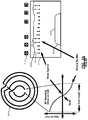
FIG. 2A illustrates an example of a voltage standing wave on the coil without the RF powered Faraday shield and corresponding deposition and sputtering on a window of the processing chamber according to the prior art; -
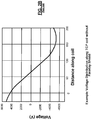
FIG. 2B is a graph illustrating an example of a voltage standing wave as a function of distance along a coil without a Faraday shield according to the prior art; -
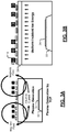
FIG. 3A illustrates an example of magnetic fields and inductive current generated by the coil with an RF-powered Faraday shield during etching according to the present disclosure; -
FIG. 3B illustrates an example of ion energy during etching using the coil with the RF-powered Faraday shield according to the present disclosure; -
FIG. 4A is an electrical schematic and functional block diagram of an example of the coil, the tuning circuit and the RF-powered Faraday shield according to the present disclosure; -
FIG. 4B is a graph illustrating a voltage standing wave forFIG. 4A ; -
FIG. 5 is an electrical schematic and functional block diagram of another example of the coil, the tuning circuit and the RF-powered Faraday shield according to the present disclosure; -
FIG. 6A is an electrical schematic and functional block diagram of another example of the coil, the tuning circuit and the RF-powered Faraday shield according to the present disclosure; and -
FIG. 6B is a graph illustrating a voltage standing wave forFIG. 6A . - In the drawings, reference numbers may be reused to identify similar and/or identical elements.
- Referring now to
FIG. 1A , an example of asubstrate processing system 10 according to the present disclosure is shown. Thesubstrate processing system 10 includes anRF generator 11. In some examples, theRF generator 11 includes anRF source 12 and atuning circuit 13. Thetuning circuit 13 tunes an output of theRF source 12 to a desired frequency and/or a desired phase and matches an impedance of acoil 16. In some examples, the output of theRF source 12 is 50 Ohms, although other values may be used. While a single coil is shown, multiple coils may be used. - In some examples, an RF powered
Faraday shield 20 may be arranged between thecoil 16 and adielectric window 24. The RF-poweredFaraday shield 20 may be connected to a tap on thecoil 16. InFIG. 1B , the RF-poweredFaraday shield 20 includes a mesh of conductive material arranged adjacent to thedielectric window 24. - The
dielectric window 24 is arranged along one side of aprocessing chamber 28. Theprocessing chamber 28 further comprises a substrate support (or pedestal) 32. Asubstrate 34 is arranged on thesubstrate support 32 during processing. Thesubstrate support 32 may include an electrostatic chuck (ESC), a mechanical chuck or other type of chuck. Process gas is supplied to theprocessing chamber 28 andplasma 40 is generated inside of theprocessing chamber 28. Theplasma 40 etches an exposed surface of thesubstrate 34. In some examples, anRF source 50 and abias matching circuit 52 may be used to bias thesubstrate support 32 during operation to further control ion energy. - A
gas delivery system 56 may be used to supply an etch gas mixture to theprocessing chamber 28. Thegas delivery system 56 may include etch gas andinert gas sources 57, agas metering system 58 such as valves and mass flow controllers, and a manifold 59. In some examples, the process gas includes an etch gas mixture. In some examples, the etch gas includes a PZT etch gas mixture. A heater/cooler 64 may be used to heat/cool thesubstrate support 32 to a predetermined temperature. Anexhaust system 65 includes a valve 66 and pump 67 to remove reactants from theprocessing chamber 28 by purging or evacuation. - A
controller 54 may be used to control the etching process. Thecontroller 54 monitors system parameters and controls delivery of the gas mixture, striking, maintaining and extinguishing the plasma, removal of reactants, supply of cooling gas, etc. Additionally, as described below in detail, thecontroller 54 may control various aspects of theRF generator 11, theRF source 50, and thebias matching circuit 52, etc. - Referring now to
FIGs. 2A and2B , a voltage standing wave (VSW) on the coil is shown as a function of coil length for the applications that do not use the RF-poweredFaraday shield 20. InFIG. 2A , ions incident on the dielectric window have energy that varies with a magnitude of the voltage standing wave on the coil. As a result, sputtering of the dielectric window occurs in locations of the coil corresponding to high voltage magnitudes of the voltage standing wave. Deposition on the dielectric window occurs in locations of the coil corresponding to low voltage magnitudes of the voltage standing wave. In other words, byproducts of the PZT etching will be deposited on the dielectric window. InFIG. 2B , an example voltage distribution along the coil without a Faraday shield is shown. As can be appreciated, connecting the RF-poweredFaraday shield 20 will change the voltage standing wave on thecoil 16. - Referring now to
FIGs. 3A and 3B , operation of the coil is shown with the RF-poweredFaraday shield 20. InFIG. 3A , thecoils 16 and the RF-poweredFaraday shield 20 induce a magnetic field and inductive current as shown. InFIG. 3B , ions have substantially uniform ion energy across thedielectric window 24 in contrast to the variable energy of the ions inFIGs. 2A and2B . - Referring now to
FIGs. 4A and 4B , connection of the RF-poweredFaraday shield 20 to thecoil 16 is shown. InFIG. 4A , thetuning circuit 13 is shown to include variable capacitors C1, C2 and C3. One terminal of the variable capacitor C1 is connected to an output of theRF generator 11. Another terminal of the variable capacitor C1 is connected to terminals of the variable capacitors C2 and C3. Another terminal of the variable capacitor C2 is connected to a fixed reference potential such as ground. Another terminal of the variable capacitor C3 is connected to one end of thecoil 16. An opposite end of thecoil 16 is connected to a variable capacitor C4. The RF-poweredFaraday shield 20 is also connected to thecoil 16 at a tap location between opposite ends of thecoil 16. The tap location of the RF-poweredFaraday shield 20 may be varied to achieve optimum RF power and/or to vary a location of the VSW. Stray capacitance CS is shown between thecoil 16 and the RF-poweredFaraday shield 20. InFIG. 4B , a voltage Vpp is shown along a length of thecoil 16. - Referring now to
FIG. 5 , another example of the RF-poweredFaraday shield 20 is shown. The RF-poweredFaraday shield 20 is coupled by stray capacitance CS to thecoil 16. Alternately, a fixed or variable capacitor C6 (not shown) may be used to couple the RF-poweredFaraday shield 20 to thecoil 16. A variable capacitor C5 may be used to adjust the effect of the RF-poweredFaraday shield 20 and/or to adjust a location of the VSW. In some examples, the variable capacitor C5 has a capacitance in a range between 8 pF and 650 pF, although other values may be used. - Referring now to
FIGs. 6A and 6B , another example of the RF-poweredFaraday shield 20 is shown. InFIG. 6A , the RF-poweredFaraday shield 20 is directly connected to a tap location between opposite ends of thecoil 16. The RF-poweredFaraday shield 20 is also coupled to thecoil 16 by stray capacitance CS. A variable capacitor C5 is connected to the RF-poweredFaraday shield 20. InFIG. 6B , the voltage Vpp is shown along the length of the coil between the terminal corresponding to the variable capacitor C3 and the terminal corresponding to the capacitor C4. The RF-poweredFaraday shield 20 is supplied directly by RF voltage on thecoil 16. The VSW can be adjusted using the variable capacitor C5. - By using the RF-powered Faraday shield, byproduct deposition on the dielectric window is significantly reduced during etching. In some examples, the etching includes PZT etching. Since the RF-powered Faraday shield voltage is reduced, RF coupling to the dielectric window is also reduced. As a result, performance and repeatability of the process improves. As can be appreciated, the variable capacitors can be fixed capacitors and vice versa.
- The foregoing description is merely illustrative in nature and is in no way intended to limit the disclosure, its application, or uses. The broad teachings of the disclosure can be implemented in a variety of forms. Therefore, while this disclosure includes particular examples, the true scope of the disclosure should not be so limited since other modifications will become apparent upon a study of the drawings, the specification, and the following claims. It should be understood that one or more steps within a method may be executed in different order (or concurrently) without altering the principles of the present disclosure. Further, although each of the embodiments is described above as having certain features, any one or more of those features described with respect to any embodiment of the disclosure can be implemented in and/or combined with features of any of the other embodiments, even if that combination is not explicitly described. In other words, the described embodiments are not mutually exclusive, and permutations of one or more embodiments with one another remain within the scope of this disclosure.
- Spatial and functional relationships between elements (for example, between modules, circuit elements, semiconductor layers, etc.) are described using various terms, including "connected," "engaged," "coupled," "adjacent," "next to," "on top of," "above," "below," and "disposed." Unless explicitly described as being "direct," when a relationship between first and second elements is described in the above disclosure, that relationship can be a direct relationship where no other intervening elements are present between the first and second elements, but can also be an indirect relationship where one or more intervening elements are present (either spatially or functionally) between the first and second elements. As used herein, the phrase at least one of A, B, and C should be construed to mean a logical (A OR B OR C), using a non-exclusive logical OR, and should not be construed to mean "at least one of A, at least one of B, and at least one of C."
- In some implementations, a controller is part of a system, which may be part of the above-described examples. Such systems can comprise semiconductor processing equipment, including a processing tool or tools, chamber or chambers, a platform or platforms for processing, and/or specific processing components (a wafer pedestal, a gas flow system, etc.). These systems may be integrated with electronics for controlling their operation before, during, and after processing of a semiconductor wafer or substrate. The electronics may be referred to as the "controller," which may control various components or subparts of the system or systems. The controller, depending on the processing requirements and/or the type of system, may be programmed to control any of the processes disclosed herein, including the delivery of processing gases, temperature settings (e.g., heating and/or cooling), pressure settings, vacuum settings, power settings, radio frequency (RF) generator settings, RF matching circuit settings, frequency settings, flow rate settings, fluid delivery settings, positional and operation settings, wafer transfers into and out of a tool and other transfer tools and/or load locks connected to or interfaced with a specific system.
- Broadly speaking, the controller may be defined as electronics having various integrated circuits, logic, memory, and/or software that receive instructions, issue instructions, control operation, enable cleaning operations, enable endpoint measurements, and the like. The integrated circuits may include chips in the form of firmware that store program instructions, digital signal processors (DSPs), chips defined as application specific integrated circuits (ASICs), and/or one or more microprocessors, or microcontrollers that execute program instructions (e.g., software). Program instructions may be instructions communicated to the controller in the form of various individual settings (or program files), defining operational parameters for carrying out a particular process on or for a semiconductor wafer or to a system. The operational parameters may, in some embodiments, be part of a recipe defined by process engineers to accomplish one or more processing steps during the fabrication of one or more layers, materials, metals, oxides, silicon, silicon dioxide, surfaces, circuits, and/or dies of a wafer.
- The controller, in some implementations, may be a part of or coupled to a computer that is integrated with the system, coupled to the system, otherwise networked to the system, or a combination thereof. For example, the controller may be in the "cloud" or all or a part of a fab host computer system, which can allow for remote access of the wafer processing. The computer may enable remote access to the system to monitor current progress of fabrication operations, examine a history of past fabrication operations, examine trends or performance metrics from a plurality of fabrication operations, to change parameters of current processing, to set processing steps to follow a current processing, or to start a new process. In some examples, a remote computer (e.g. a server) can provide process recipes to a system over a network, which may include a local network or the Internet. The remote computer may include a user interface that enables entry or programming of parameters and/or settings, which are then communicated to the system from the remote computer. In some examples, the controller receives instructions in the form of data, which specify parameters for each of the processing steps to be performed during one or more operations. It should be understood that the parameters may be specific to the type of process to be performed and the type of tool that the controller is configured to interface with or control. Thus as described above, the controller may be distributed, such as by comprising one or more discrete controllers that are networked together and working towards a common purpose, such as the processes and controls described herein. An example of a distributed controller for such purposes would be one or more integrated circuits on a chamber in communication with one or more integrated circuits located remotely (such as at the platform level or as part of a remote computer) that combine to control a process on the chamber.
- Without limitation, example systems may include a plasma etch chamber or module, a deposition chamber or module, a spin-rinse chamber or module, a metal plating chamber or module, a clean chamber or module, a bevel edge etch chamber or module, a physical vapor deposition (PVD) chamber or module, a chemical vapor deposition (CVD) chamber or module, an atomic layer deposition (ALD) chamber or module, an atomic layer etch (ALE) chamber or module, an ion implantation chamber or module, a track chamber or module, and any other semiconductor processing systems that may be associated or used in the fabrication and/or manufacturing of semiconductor wafers.
- As noted above, depending on the process step or steps to be performed by the tool, the controller might communicate with one or more of other tool circuits or modules, other tool components, cluster tools, other tool interfaces, adjacent tools, neighboring tools, tools located throughout a factory, a main computer, another controller, or tools used in material transport that bring containers of wafers to and from tool locations and/or load ports in a semiconductor manufacturing factory.
Claims (15)
- A substrate processing system comprising:a processing chamber including a dielectric window and a substrate support arranged therein to support a substrate;a coil arranged outside of the processing chamber adjacent to the dielectric window;a Faraday shield arranged between the coil and the dielectric window; andan RF generator configured to supply RF power to the coil.
- The substrate processing system of claim 1, further comprising a capacitor connected to one of the coil and the Faraday shield to alter a position of a voltage standing wave along the coil.
- The substrate processing system of claim 1, further comprising a tuning circuit arranged between the RF generator and the coil.
- The substrate processing system of claim 3, wherein the tuning circuit includes:a first variable capacitor including a first end connected to the RF generator and a second end;a second variable capacitor including a first end connected to the second end of the first variable capacitor; anda third variable capacitor including a first end and a second end, wherein the first end of the third variable capacitor is connected to the second end of the first variable capacitor and the first end of the second variable capacitor and the second end of the third variable capacitor is connected to the coil.
- The substrate processing system of claim 3, wherein:the coil includes a first end and a second end;the tuning circuit is connected to the first end; andthe second end is connected to the Faraday shield.
- The substrate processing system of claim 5, wherein the second end corresponds to a center tap of the coil; or
the substrate processing system further comprising a capacitor including one end connected to the second end and an opposite end connected to a fixed reference potential. - The substrate processing system of claim 3, wherein:the coil includes a first end and a second end;the tuning circuit is connected to the first end of the coil; andthe coil is coupled by stray capacitance to the Faraday shield.
- The substrate processing system of claim 7, further comprising a first capacitor including a first end connected to the Faraday shield and a second end connected to a fixed reference potential.
- The substrate processing system of claim 7, further comprising a first capacitor including a first end connected to the coil and a second end connected to a fixed reference potential.
- The substrate processing system of claim 7, further comprising:a first capacitor including a first end connected to the Faraday shield and a second end connected to a fixed reference potential; anda second capacitor including a first end connected to the coil and a second end connected to a fixed reference potential.
- The substrate processing system of claim 3, wherein:the coil includes a first end and a second end;the tuning circuit is connected to the first end of the coil;the second end of the coil is connected to the Faraday shield; andthe coil is coupled by stray capacitance to the Faraday shield.
- The substrate processing system of claim 11, wherein the second end corresponds to a center tap of the coil.
- The substrate processing system of claim 11, further comprising a capacitor including one end connected to the second end and an opposite end connected to a fixed reference potential; or
further comprising a capacitor including a first end connected to the Faraday shield and a second end connected to a fixed reference potential. - The substrate processing system of claim 11, further comprising:a first capacitor including one end connected to the second end and an opposite end connected to a fixed reference potential.a second capacitor including a first end connected to the Faraday shield and a second end connected to a fixed reference potential.
- The substrate processing system of claim 1, wherein the Faraday shield comprises a wire mesh.
Applications Claiming Priority (1)
| Application Number | Priority Date | Filing Date | Title |
|---|---|---|---|
| US201662314059P | 2016-03-28 | 2016-03-28 |
Publications (1)
| Publication Number | Publication Date |
|---|---|
| EP3226280A1 true EP3226280A1 (en) | 2017-10-04 |
Family
ID=58547309
Family Applications (1)
| Application Number | Title | Priority Date | Filing Date |
|---|---|---|---|
| EP17162738.3A Withdrawn EP3226280A1 (en) | 2016-03-28 | 2017-03-24 | Substrate processing system including a coil with an rf powered faraday shield |
Country Status (5)
| Country | Link |
|---|---|
| US (2) | US20170278680A1 (en) |
| EP (1) | EP3226280A1 (en) |
| KR (1) | KR102382273B1 (en) |
| CN (1) | CN107240542A (en) |
| TW (1) | TWI753891B (en) |
Cited By (1)
| Publication number | Priority date | Publication date | Assignee | Title |
|---|---|---|---|---|
| TWI914357B (en) | 2020-05-27 | 2026-02-11 | 美商蘭姆研究公司 | Substrate processing system |
Families Citing this family (7)
| Publication number | Priority date | Publication date | Assignee | Title |
|---|---|---|---|---|
| US11189464B2 (en) | 2019-07-17 | 2021-11-30 | Beijing E-town Semiconductor Technology Co., Ltd. | Variable mode plasma chamber utilizing tunable plasma potential |
| CN110223904A (en) * | 2019-07-19 | 2019-09-10 | 江苏鲁汶仪器有限公司 | A kind of plasma process system with Faraday shield device |
| CN110416053B (en) * | 2019-07-30 | 2021-03-16 | 江苏鲁汶仪器有限公司 | Inductively coupled plasma processing system |
| CN114514602B (en) * | 2019-09-27 | 2025-11-07 | 朗姆研究公司 | Adjustable and non-adjustable heat shield for influencing the temperature distribution profile of a substrate support |
| US12334312B2 (en) | 2020-12-28 | 2025-06-17 | Beijing E-town Semiconductor Technology Co., Ltd. | Configurable faraday shield |
| CN113533308A (en) * | 2021-06-15 | 2021-10-22 | 杭州谱育科技发展有限公司 | Device and method for detecting elements in radioactive sample |
| US12597588B2 (en) * | 2023-05-17 | 2026-04-07 | Applied Materials, Inc. | Inductively coupled plasma apparatus with novel faraday shield |
Citations (3)
| Publication number | Priority date | Publication date | Assignee | Title |
|---|---|---|---|---|
| WO2001075930A2 (en) * | 2000-03-31 | 2001-10-11 | Lam Research Corporation | Apparatus and methods for actively controlling rf peak-to-peak voltage in an inductively coupled plasma etching system |
| US20050194355A1 (en) * | 2002-07-31 | 2005-09-08 | Lam Research Corporation | Method for adjusting voltage on a powered faraday shield |
| US20060175016A1 (en) * | 2005-02-07 | 2006-08-10 | Manabu Edamura | Plasma processing apparatus |
Family Cites Families (9)
| Publication number | Priority date | Publication date | Assignee | Title |
|---|---|---|---|---|
| US6063234A (en) * | 1997-09-10 | 2000-05-16 | Lam Research Corporation | Temperature sensing system for use in a radio frequency environment |
| US6280563B1 (en) * | 1997-12-31 | 2001-08-28 | Lam Research Corporation | Plasma device including a powered non-magnetic metal member between a plasma AC excitation source and the plasma |
| US6442173B1 (en) | 1999-04-07 | 2002-08-27 | Legerity | Timing recovery scheme for a discrete multitone transmission system |
| US6422173B1 (en) * | 2000-06-30 | 2002-07-23 | Lam Research Corporation | Apparatus and methods for actively controlling RF peak-to-peak voltage in an inductively coupled plasma etching system |
| US20070017867A1 (en) * | 2005-07-21 | 2007-01-25 | Pedros Philip B | Submerged attached growth bioreactor |
| CN101390187A (en) * | 2006-01-24 | 2009-03-18 | 瓦里安半导体设备公司 | Plasma Ionization Source with Low Effective Antenna Voltage |
| US20070170867A1 (en) * | 2006-01-24 | 2007-07-26 | Varian Semiconductor Equipment Associates, Inc. | Plasma Immersion Ion Source With Low Effective Antenna Voltage |
| GB201002283D0 (en) * | 2010-02-10 | 2010-03-31 | Ceravision Ltd | Light source |
| JP6715129B2 (en) * | 2016-08-31 | 2020-07-01 | 東京エレクトロン株式会社 | Plasma processing device |
-
2017
- 2017-03-23 US US15/467,588 patent/US20170278680A1/en not_active Abandoned
- 2017-03-24 EP EP17162738.3A patent/EP3226280A1/en not_active Withdrawn
- 2017-03-27 TW TW106110091A patent/TWI753891B/en active
- 2017-03-27 KR KR1020170038506A patent/KR102382273B1/en active Active
- 2017-03-28 CN CN201710193556.0A patent/CN107240542A/en active Pending
-
2020
- 2020-09-10 US US17/016,888 patent/US12087557B2/en active Active
Patent Citations (3)
| Publication number | Priority date | Publication date | Assignee | Title |
|---|---|---|---|---|
| WO2001075930A2 (en) * | 2000-03-31 | 2001-10-11 | Lam Research Corporation | Apparatus and methods for actively controlling rf peak-to-peak voltage in an inductively coupled plasma etching system |
| US20050194355A1 (en) * | 2002-07-31 | 2005-09-08 | Lam Research Corporation | Method for adjusting voltage on a powered faraday shield |
| US20060175016A1 (en) * | 2005-02-07 | 2006-08-10 | Manabu Edamura | Plasma processing apparatus |
Cited By (1)
| Publication number | Priority date | Publication date | Assignee | Title |
|---|---|---|---|---|
| TWI914357B (en) | 2020-05-27 | 2026-02-11 | 美商蘭姆研究公司 | Substrate processing system |
Also Published As
| Publication number | Publication date |
|---|---|
| KR102382273B1 (en) | 2022-04-01 |
| US12087557B2 (en) | 2024-09-10 |
| KR20170113281A (en) | 2017-10-12 |
| TWI753891B (en) | 2022-02-01 |
| TW201802861A (en) | 2018-01-16 |
| US20170278680A1 (en) | 2017-09-28 |
| US20200411297A1 (en) | 2020-12-31 |
| CN107240542A (en) | 2017-10-10 |
Similar Documents
| Publication | Publication Date | Title |
|---|---|---|
| US12087557B2 (en) | Substrate processing system including coil with RF powered faraday shield | |
| US10847345B2 (en) | Direct drive RF circuit for substrate processing systems | |
| US10879044B2 (en) | Auxiliary circuit in RF matching network for frequency tuning assisted dual-level pulsing | |
| US11728137B2 (en) | Direct frequency tuning for matchless plasma source in substrate processing systems | |
| US10262887B2 (en) | Pin lifter assembly with small gap | |
| US12322579B2 (en) | Metal contamination reduction in substrate processing systems with transformer coupled plasma | |
| US10332725B2 (en) | Systems and methods for reversing RF current polarity at one output of a multiple output RF matching network | |
| US20250079121A1 (en) | Dual-frequency, direct-drive inductively coupled plasma source | |
| US10347464B2 (en) | Cycle-averaged frequency tuning for low power voltage mode operation | |
| US20250054738A1 (en) | Tunable esc for rapid alternating process applications | |
| KR20210034095A (en) | RF power compensation to reduce deposition rate or etch rate variations in response to substrate bulk resistivity variations | |
| WO2020028256A1 (en) | Honeycomb injector with dielectric window for substrate processing systems |
Legal Events
| Date | Code | Title | Description |
|---|---|---|---|
| PUAI | Public reference made under article 153(3) epc to a published international application that has entered the european phase |
Free format text: ORIGINAL CODE: 0009012 |
|
| AK | Designated contracting states |
Kind code of ref document: A1 Designated state(s): AL AT BE BG CH CY CZ DE DK EE ES FI FR GB GR HR HU IE IS IT LI LT LU LV MC MK MT NL NO PL PT RO RS SE SI SK SM TR |
|
| AX | Request for extension of the european patent |
Extension state: BA ME |
|
| 17P | Request for examination filed |
Effective date: 20180403 |
|
| RBV | Designated contracting states (corrected) |
Designated state(s): AL AT BE BG CH CY CZ DE DK EE ES FI FR GB GR HR HU IE IS IT LI LT LU LV MC MK MT NL NO PL PT RO RS SE SI SK SM TR |
|
| 17Q | First examination report despatched |
Effective date: 20190926 |
|
| STAA | Information on the status of an ep patent application or granted ep patent |
Free format text: STATUS: THE APPLICATION IS DEEMED TO BE WITHDRAWN |
|
| 18D | Application deemed to be withdrawn |
Effective date: 20200718 |