EP3225399A1 - Printing apparatus - Google Patents
Printing apparatus Download PDFInfo
- Publication number
- EP3225399A1 EP3225399A1 EP17163682.2A EP17163682A EP3225399A1 EP 3225399 A1 EP3225399 A1 EP 3225399A1 EP 17163682 A EP17163682 A EP 17163682A EP 3225399 A1 EP3225399 A1 EP 3225399A1
- Authority
- EP
- European Patent Office
- Prior art keywords
- rank
- actuators
- power
- power circuits
- power circuit
- Prior art date
- Legal status (The legal status is an assumption and is not a legal conclusion. Google has not performed a legal analysis and makes no representation as to the accuracy of the status listed.)
- Granted
Links
Images






Classifications
-
- B—PERFORMING OPERATIONS; TRANSPORTING
- B41—PRINTING; LINING MACHINES; TYPEWRITERS; STAMPS
- B41J—TYPEWRITERS; SELECTIVE PRINTING MECHANISMS, i.e. MECHANISMS PRINTING OTHERWISE THAN FROM A FORME; CORRECTION OF TYPOGRAPHICAL ERRORS
- B41J2/00—Typewriters or selective printing mechanisms characterised by the printing or marking process for which they are designed
- B41J2/005—Typewriters or selective printing mechanisms characterised by the printing or marking process for which they are designed characterised by bringing liquid or particles selectively into contact with a printing material
- B41J2/01—Ink jet
- B41J2/015—Ink jet characterised by the jet generation process
- B41J2/02—Ink jet characterised by the jet generation process generating a continuous ink jet
- B41J2/035—Ink jet characterised by the jet generation process generating a continuous ink jet by electric or magnetic field
-
- B—PERFORMING OPERATIONS; TRANSPORTING
- B41—PRINTING; LINING MACHINES; TYPEWRITERS; STAMPS
- B41J—TYPEWRITERS; SELECTIVE PRINTING MECHANISMS, i.e. MECHANISMS PRINTING OTHERWISE THAN FROM A FORME; CORRECTION OF TYPOGRAPHICAL ERRORS
- B41J2/00—Typewriters or selective printing mechanisms characterised by the printing or marking process for which they are designed
- B41J2/005—Typewriters or selective printing mechanisms characterised by the printing or marking process for which they are designed characterised by bringing liquid or particles selectively into contact with a printing material
- B41J2/01—Ink jet
- B41J2/015—Ink jet characterised by the jet generation process
- B41J2/04—Ink jet characterised by the jet generation process generating single droplets or particles on demand
- B41J2/045—Ink jet characterised by the jet generation process generating single droplets or particles on demand by pressure, e.g. electromechanical transducers
- B41J2/04501—Control methods or devices therefor, e.g. driver circuits, control circuits
- B41J2/04541—Specific driving circuit
-
- B—PERFORMING OPERATIONS; TRANSPORTING
- B41—PRINTING; LINING MACHINES; TYPEWRITERS; STAMPS
- B41J—TYPEWRITERS; SELECTIVE PRINTING MECHANISMS, i.e. MECHANISMS PRINTING OTHERWISE THAN FROM A FORME; CORRECTION OF TYPOGRAPHICAL ERRORS
- B41J2/00—Typewriters or selective printing mechanisms characterised by the printing or marking process for which they are designed
- B41J2/005—Typewriters or selective printing mechanisms characterised by the printing or marking process for which they are designed characterised by bringing liquid or particles selectively into contact with a printing material
- B41J2/01—Ink jet
- B41J2/015—Ink jet characterised by the jet generation process
- B41J2/04—Ink jet characterised by the jet generation process generating single droplets or particles on demand
- B41J2/045—Ink jet characterised by the jet generation process generating single droplets or particles on demand by pressure, e.g. electromechanical transducers
- B41J2/04501—Control methods or devices therefor, e.g. driver circuits, control circuits
- B41J2/04506—Control methods or devices therefor, e.g. driver circuits, control circuits aiming at correcting manufacturing tolerances
-
- B—PERFORMING OPERATIONS; TRANSPORTING
- B41—PRINTING; LINING MACHINES; TYPEWRITERS; STAMPS
- B41J—TYPEWRITERS; SELECTIVE PRINTING MECHANISMS, i.e. MECHANISMS PRINTING OTHERWISE THAN FROM A FORME; CORRECTION OF TYPOGRAPHICAL ERRORS
- B41J2/00—Typewriters or selective printing mechanisms characterised by the printing or marking process for which they are designed
- B41J2/005—Typewriters or selective printing mechanisms characterised by the printing or marking process for which they are designed characterised by bringing liquid or particles selectively into contact with a printing material
- B41J2/01—Ink jet
- B41J2/015—Ink jet characterised by the jet generation process
- B41J2/04—Ink jet characterised by the jet generation process generating single droplets or particles on demand
- B41J2/045—Ink jet characterised by the jet generation process generating single droplets or particles on demand by pressure, e.g. electromechanical transducers
- B41J2/04501—Control methods or devices therefor, e.g. driver circuits, control circuits
- B41J2/04581—Control methods or devices therefor, e.g. driver circuits, control circuits controlling heads based on piezoelectric elements
-
- B—PERFORMING OPERATIONS; TRANSPORTING
- B41—PRINTING; LINING MACHINES; TYPEWRITERS; STAMPS
- B41J—TYPEWRITERS; SELECTIVE PRINTING MECHANISMS, i.e. MECHANISMS PRINTING OTHERWISE THAN FROM A FORME; CORRECTION OF TYPOGRAPHICAL ERRORS
- B41J2/00—Typewriters or selective printing mechanisms characterised by the printing or marking process for which they are designed
- B41J2/005—Typewriters or selective printing mechanisms characterised by the printing or marking process for which they are designed characterised by bringing liquid or particles selectively into contact with a printing material
- B41J2/01—Ink jet
- B41J2/015—Ink jet characterised by the jet generation process
- B41J2/04—Ink jet characterised by the jet generation process generating single droplets or particles on demand
- B41J2/045—Ink jet characterised by the jet generation process generating single droplets or particles on demand by pressure, e.g. electromechanical transducers
- B41J2/04501—Control methods or devices therefor, e.g. driver circuits, control circuits
- B41J2/04586—Control methods or devices therefor, e.g. driver circuits, control circuits controlling heads of a type not covered by groups B41J2/04575 - B41J2/04585, or of an undefined type
-
- B—PERFORMING OPERATIONS; TRANSPORTING
- B41—PRINTING; LINING MACHINES; TYPEWRITERS; STAMPS
- B41J—TYPEWRITERS; SELECTIVE PRINTING MECHANISMS, i.e. MECHANISMS PRINTING OTHERWISE THAN FROM A FORME; CORRECTION OF TYPOGRAPHICAL ERRORS
- B41J2/00—Typewriters or selective printing mechanisms characterised by the printing or marking process for which they are designed
- B41J2/005—Typewriters or selective printing mechanisms characterised by the printing or marking process for which they are designed characterised by bringing liquid or particles selectively into contact with a printing material
- B41J2/01—Ink jet
- B41J2/015—Ink jet characterised by the jet generation process
- B41J2/04—Ink jet characterised by the jet generation process generating single droplets or particles on demand
- B41J2/045—Ink jet characterised by the jet generation process generating single droplets or particles on demand by pressure, e.g. electromechanical transducers
- B41J2/04501—Control methods or devices therefor, e.g. driver circuits, control circuits
- B41J2/0459—Height of the driving signal being adjusted
-
- B—PERFORMING OPERATIONS; TRANSPORTING
- B41—PRINTING; LINING MACHINES; TYPEWRITERS; STAMPS
- B41J—TYPEWRITERS; SELECTIVE PRINTING MECHANISMS, i.e. MECHANISMS PRINTING OTHERWISE THAN FROM A FORME; CORRECTION OF TYPOGRAPHICAL ERRORS
- B41J2/00—Typewriters or selective printing mechanisms characterised by the printing or marking process for which they are designed
- B41J2/005—Typewriters or selective printing mechanisms characterised by the printing or marking process for which they are designed characterised by bringing liquid or particles selectively into contact with a printing material
- B41J2/01—Ink jet
- B41J2/07—Ink jet characterised by jet control
Definitions
- the present invention relates to a printing apparatus jetting ink from nozzles.
- the nozzles When the same drive voltage is applied respectively to nozzles, the nozzles have different jetting amounts (jetting velocities) of liquid droplets according to the properties of the nozzles. Conventionally, therefore, such liquid droplet jet apparatuses have been proposed as to select an optimal drive voltage for each nozzle such that the jetting amounts of liquid droplets from the nozzles may be equalized (for example, see Japanese Patent Application Laid-open No. 2008-173910 ).
- the present teaching is made in view of the above situation, and an object thereof is to provide a printing apparatus capable of providing a plurality of power circuits while downsizing the power circuits to restrain the apparatus from growing in size.
- a printing apparatus including: actuators configured to exert force to liquid; power circuits configured to apply voltages to the actuators; a switching circuit configured to switch connection destination of each of the actuators to any of the power circuits; and a controller configured to control driving of the actuators, wherein each of the actuators is associated with one of ranks which represent magnitudes of the applying voltages, and the controller is configured to allocate at least two of the power circuits to a maximum rank, of the ranks, having the largest number of actuators associated therewith.
- a plurality of power circuits can be provided while downsizing the power circuits to restrain the apparatus from growing in size.
- the power circuits may include a standby power circuit corresponding to a standby power source, and the controller may be configured to allocate the standby power circuit to the maximum rank.
- each of the power circuits may be configured to apply voltage to a predetermined number or less of actuators
- the controller may be configured to: whenever one power circuit among the power circuits is allocated to one rank among the ranks, for the one rank to which the one power circuit is allocated, calculate a second number of actuators by subtracting the predetermined number from the number of actuators before allocating the one power circuit; allocate the power circuits to the ranks in descending order of the number of actuators and the second number of actuators associated therewith; determine whether there is any unallocated rank without any power circuit, among the power circuits, allocated thereto, after each of the power circuits is allocated to any of the ranks; and based on determining that there is an unallocated rank, allocate, to the unallocated rank, one of the power circuits which has the closest voltage to the voltage of the unallocated rank.
- each of the power circuits may be configured to apply voltage to a predetermined number or less of the actuators
- the controller may be configured to: select the maximum rank; determine whether the number of actuators associated with the selected rank is not more than the predetermined number; based on determining that the number of actuators associated with the selected rank is not more than the predetermined number, allocate the power circuits to the ranks in descending order of the number of actuators associated therewith; based on determining that the number of actuators associated with the selected rank is more than the predetermined number, calculate a value of dividing the number of actuators associated with the selected rank by the predetermined number; divide the number of actuators associated with the selected rank by the value to calculate a sub number of actuators; allocate the power circuits to the ranks in descending order of the number of actuators and the sub number of actuators associated therewith; determine whether there is any unallocated rank without any power circuit, among the power circuits, allocated thereto, after each of the power circuits is allocated to
- the controller may be configured to, after calculating the sub number of actuators, select another rank having the second largest number of actuators next to the selected rank.
- a maximum allocation number of the power circuits allocatable to each of the ranks may be preset, each of the power circuits may be configured to apply voltage to a predetermined number or less of the actuators, and the controller may be configured to: whenever one power circuit among the power circuits is allocated to one rank among the ranks, for the one rank to which the one power circuit is allocated, calculate a second number of actuators by subtracting the predetermined number from the number of actuators before allocating the one power circuit; allocate a number of power circuits not more than the maximum allocation number to the maximum rank, and allocate a number of the power circuits less than the maximum allocation number to each of the other ranks; determine whether the number of actuators associated with the maximum rank is more than the total number of the predetermined numbers of all of the power circuits allocated to the maximum rank; based on determining that the number of actuators associated with the maximum rank is more than the total number of the predetermined numbers of all of the power circuits allocated to the maximum rank, calculate a value by
- the controller may be configured to: divide the same number as the value of actuators associated with the maximum rank; and allocate the divided actuators respectively to the other ranks.
- the predetermined number may be set according to a property of each of the power circuits, a drive voltage for each of the actuators, the number of actuators, a drive frequency of each of the actuators, or a temperature.
- the power circuits may include at least one first power circuit where the predetermined number is a first number, and at least one second power circuit where the predetermined number is a second number different from the first number, and one of the second power circuits may be arranged between two of the first power circuits or one of the first power circuits may be arranged between two of the second power circuits.
- the actuators may form a plurality of rows arranged in one direction, and under a condition that, among the plurality of rows, there are multiple rows belonging to one rank among the ranks and being consecutive in the one direction, and under a condition that one power circuit among the power circuits is allocated to the one rank, the controller may be configured to allocate the power circuits to the plurality of rows such that the one power circuit is not consecutive or the number of the one power circuit consecutive in the one direction is not more than a predetermined number.
- a printing apparatus including: actuators configured to exert force to liquid; power circuits configured to apply voltages to the actuators; and a switching circuit configured to switch connection destination of each of the actuators to any of the power circuits, wherein the actuators are divided into actuator groups according to the voltage of driving each of the actuators, and at least two of the power circuits are connected to an actuator group, of the actuator groups, having the largest number of actuators included therein, by the switching circuit.
- the front side of a printing apparatus 1 is defined on the downstream side in a conveyance direction of recording paper 100, whereas the rear side of the printing apparatus 1 is defined on the upstream side in the conveyance direction.
- the left-right direction of the printing apparatus 1 is defined in such a direction along the paper width as is parallel to the conveyance plane of the recording paper 100 (the plane parallel to the page of Fig. 1 ) and is orthogonal to the conveyance direction.
- the left side of Fig. 1 is the left side of the printing apparatus 1
- the right side of Fig. 1 is the right side of the printing apparatus 1.
- the upper-lower or vertical direction of the printing apparatus 1 is defined in a direction orthogonal to the conveyance plane of the recording paper 100 (a direction orthogonal to the page of Fig. 1 ).
- the front or near side of the page is the upper side whereas the rear side or far side of the page is the lower side.
- Those defined front, rear, left, right, upper, and lower will be used appropriately in the following explanation.
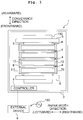
- the printing apparatus 1 includes a casing 2, a platen 3, four ink-jet heads 4, two conveyance rollers 5 and 6, and a controller 7.
- the platen 3 is placed horizontally in the casing 2.
- the recording paper 100 is placed on the upper surface of the platen 3.
- the four ink-jet heads 4 are provided above the platen 3 to be juxtaposed in the front-rear direction.
- the two conveyance rollers 5 and 6 are arranged respectively on the rear side and the front side of the platen 3.
- the two conveyance rollers 5 and 6 are driven respectively by an undepicted motor to convey the recording paper 100 on the platen 3 to the front side.
- the controller 7 includes non-volatile memories and the like such as a plurality of FPGAs 71a and 72a (Field Programmable Gate Array; see Fig. 4 ), a ROM (Read Only Memory), a RAM (Random Access Memory), and an EEPROM (Electrically Erasable Programmable Read-Only Memory). Further, illustration of the ROM, RAM, EEPROM and the like is omitted here. Further, the controller 7 is connected with an external device 9 such as a PC or the like in a data communicable manner, to control each device of the printing apparatus 1 based on print data sent from the external device 9.
- an external device 9 such as a PC or the like in a data communicable manner
- the controller 7 controls the motor for driving the conveyance rollers 5 and 6 to cause the conveyance rollers 5 and 6 to convey the recording paper 100 in the conveyance direction. Further, the controller 7 controls the ink-jet heads 4 to jet inks toward the recording paper 100. By virtue of this, image is printed on the recording paper 100.
- Head holders 8 are installed in the casing 2.
- the head holders 8 are arranged above the platen 3 and juxtaposed in the front-rear direction between the conveyance rollers 5 and 6.
- the head holders 8 hold the ink-jet heads 4 respectively.
- the four ink-jet heads 4 respectively jet the inks of four colors: cyan (C), magenta (M), yellow (y), and black (K). Each of the ink-jet heads 4 is supplied with the ink of the corresponding color from an undepicted ink tank.
- each of the ink-jet heads 4 includes a holder 10 in a rectangular plate-like shape elongated in the paper width direction, and head units 11 attached to the holder 10.
- a plurality of nozzles 11a are formed on the lower surface of each of the head units 11.
- Each of the nozzles 11 a includes an aftermentioned piezoelectric body 11b (see Fig. 6 ).
- the plurality of nozzles 11a of each of the head units 11 are juxtaposed along the paper width direction which is the longitudinal direction of the ink-jet heads 4, and the head units 11 form a first head row 81 and a second head row 82.
- the first head row 81 and the second head row 82 are juxtaposed in the conveyance direction and the first head row 81 is positioned on the rear side of the second head row 82.
- a left end portion of each head unit 11 in the first head row 81 is at the same position as a right end portion of one head unit 11 in the second head row 82 in the left-right direction.
- the left end portion of each head unit 11 in the first head row 81 overlaps with the right end portion of one head unit 11 in the second head row 82 in the front-rear direction.
- the holder 10 is provided with a slit 10a.
- a flexible substrate 51 connects the head units 11 and the controller 7, and the flexible substrate 51 is inserted through the slit 10a.
- the head units 11 are arranged along an arrangement direction which is the paper width direction.
- the head units 11 are arranged to be alternately separate between the front side and the rear side in the conveyance direction. Between the head units 11 arranged on the front side and the head units 11 arranged on the rear side, there is a positional deviation on the left and the right (in the arrangement direction).
- the head units 11 are juxtaposed along the direction orthogonal to the conveyance direction (along the paper width direction).
- the head units 11 may be arranged obliquely, that is, along a direction intersecting the conveyance direction at an angle other than 90 degrees.
- a reservoir 12 is provided above the head units 11.
- An illustration of the reservoir 12 is omitted in Fig. 3 .
- the reservoir 12 is connected to one of the ink tanks (not depicted) via a tube 16 to temporarily retain the ink supplied from the ink tank.
- the reservoir 12 has a lower portion connected to the head units 11 to supply each of the head units 11 with the ink from the reservoir 12. Further, the head units 11 may be moved in the paper width direction.
- the controller 7 includes a first substrate 71 and a plurality of second substrates 72.
- the first substrate 71 is provided with the FPGA 71a.
- One second substrate 72 is provided with one FPGA 72a.
- the FPGA 71 a is connected to the FPGAs 72a to control the driving of the FPGAs 72a.
- the second substrates 72 that is, the FPGAs 72a correspond respectively to the plurality of head units 11, and the number of the FPGAs 72a is the same as the number of head units 11.
- the FPGAs 72a are connected respectively with the head units 11.
- the FPGA 71a and the FPGAs 72a are connected to the ROM (not depicted) storing bit stream information and to the RAM (not depicted) as a memory.
- Each of the head units 11 includes a substrate 11c on which a removable connector 11 d, a non-volatile memory 11e, and a driver IC 11f are mounted. Each of the head units 11 is connected to one of the second substrates 72 in a removable manner via the connector 11d. Each of the driver ICs 11f includes a switching circuit 27 which will be described later on.
- the second substrate 72 is provided with a D/A (Digital/Analog) converter 20. Further, the second substrate 72 is provided with a plurality of power circuits and, particularly in this embodiment, is provide with a first power circuit 21 to a sixth power circuit 26. Each of the first power circuit 21 to the sixth power circuit 26 has an FET, impedance and the like, and output voltage thereof is changeable. As those first power circuit 21 to sixth power circuit 26, for example, switching-type DC/DC converters may be adopted. The FPGA 72a outputs a signal to the first power circuit 21 to the sixth power circuit 26 via the D/A converter 20, to set the output voltage.
- D/A Digital/Analog
- the first power circuit 21 to the sixth power circuit 26 are connected to a first power wire 34(1) to an nth power wire 34(n) (n is a natural number not smaller than two) via the switching circuit 27.
- the switching circuit 27 connects each of the first power wire 34(1) to the nth power wire 34(n) to any of the first power circuit 21 to the sixth power circuit 26.
- the first power circuit 21 to the fourth power circuit 24 are ordinary power circuits which are ordinary used.
- the fifth power circuit 25 may be an ordinary power circuit or a standby power circuit while the sixth power circuit 26 is a power circuit of special specification.
- the sixth power circuit 26 is, for example, used for the highest rank of the drive voltages, or used concurrently as a power supply voltage for the VCOM of the actuators, or used for the nozzles 11a jetting the inks less easily, or used as an HVDD (the back gate voltage on the high side) of a PMOS transistor 31.
- the HVDD voltage is connected to the sixth power circuit 26 whose output voltage is higher than the first power circuit 21 to the fifth power circuit 25 such that no electric current may flow in any parasitic diode of the PMOS transistor 31 on the high side even if a higher voltage is applied to a drain terminal 31b than to a source terminal 31a of the PMOS transistor 31.
- the printing apparatus 1 is provided with a plurality of CMOS circuits 30 to respectively drive the nozzles 11a.
- the FPGAs 72a output gate signals to the CMOS circuits 30 via a first control wire 33(1) to an nth control wire 33(n) (n is a natural number not smaller than two).
- the first control wire 33(1) to the nth control wire 33(n) correspond to the first power wire 34(1) to the nth power wire 34(n). That is, the first control wire 33(1) corresponds to the first power wire 34(1), and the nth control wire 33(n) corresponds to the nth power wire 34(n).
- the FPGA 72a outputs a signal to the switching circuit 27 to connect each of the first power wire 34(1) to the nth power wire 34(n) to any of the first power circuit 21 to the sixth power circuit 26.
- the FPGA 72a accesses the non-volatile memory 11e as necessary.
- the non-volatile memory 11e stores a plurality of nozzle addresses identifying the respective nozzles 11 a, ranks corresponding to the nozzle addresses, and the like. The ranks will be described later on.
- the CMOS circuit 30 includes the PMOS (P-type Metal-Oxide-Semiconductor) transistor 31, an NMOS (N-type Metal-Oxide-Semiconductor) transistor 32, an impedance 35, two piezoelectric bodies 11b and 11b', and the like.
- the piezoelectric bodies 11b and 11b' function as capacitors. Further, only the single piezoelectric body 11b may be provided.
- the source terminal 31a of the PMOS transistor 31 is connected to any of the first power wire 34(1) to the nth power wire 34(n).
- a source terminal 32a of the NMOS transistor 32 is grounded.
- the drain terminals 31b and 32b of the PMOS transistor 31 and NMOS transistor 32 are connected to one end of the impedance 35.
- the other end of the impedance 35 is connected to the other end of the piezoelectric body 11b' on one hand and to one end of the piezoelectric body 11b on the other hand.
- the one end of the piezoelectric body 11b' on the one hand is connected to the VCOM voltage, that is, the sixth power supply voltage, whereas the other end of the piezoelectric body 11b on the other hand is grounded.
- the PMOS transistor 31 and NMOS transistor 32 have gate terminals 31c and 32c connected to any of the first control wire 33(1) to nth control wire 33(n) corresponding to the power wires connected to the source terminal 31 a of the PMOS transistor 31.
- Fig. 7 is a graph depicting a relationship between a nozzle address identifying each nozzle and a velocity of liquid droplets (ink) jetted from each nozzle 11a corresponding to the nozzle address when a certain voltage is applied to the piezoelectric bodies 11b and 11b'.
- nozzle addresses There are, for example, 1680 nozzle addresses.
- the liquid droplet velocity is set in five velocity ranges to correspond to the rank A to the rank E, respectively. Further, the rank A corresponds to the highest velocity range whereas the rank E corresponds to the lowest velocity range.
- the non-volatile memory 11e stores the rank A to the rank E according to the liquid droplet velocity of each nozzle 11a, and the corresponding respective nozzle addresses. While the liquid droplet velocity is taken as an example here, it is possible to use the same concept for the jetting amount of liquid droplets.
- the non-volatile memory 11e of the head unit 11 stores such an allocation table as in Fig. 8 , indicating an allocation of power circuits to the nozzles 11a.
- the column of the number of nozzles depicts the number of the nozzles 11a corresponding to the respective ranks, being preset in the non-volatile memory 11e according to each rank.
- the column of power source number depicts the power circuit number allocated to each rank.
- the column of drive voltage depicts the voltage for driving the nozzles 11a corresponding to each rank. In other words, the rank represents the magnitude of the voltage applied to the nozzles 11a.
- the drive voltage serves for jetting the inks from the nozzles 11a at the targeted liquid droplet velocity, and is preset in the non-volatile memory 11e for each rank to suppress the difference in the liquid droplet velocity between the nozzles 11a.
- the power source numbers 1 to 6 correspond respectively to the first power circuit 21 to the sixth power circuit 26.
- the number of nozzles in each of the ranks A to E is calculated in advance with a method including actual measurement.
- the calculated number of nozzles is stored in a table in the non-volatile memory 11e.
- the number of nozzles included in the ranks A to E are, respectively, 10, 350, 800, 500, and 20.
- the power source number 6 is allocated to the rank E of the highest drive voltage. Further, in descending order of the number of nozzles, the ordinary power circuits, that is, the first power circuit 21 to the fourth power circuit 24, are allocated respectively to the ranks A to D.
- the power circuit number of the allocated power circuit is stored in the table. For example, as depicted in Fig. 8 , the power source numbers 4, 3, 1,2 and 6 are allocated respectively to the ranks A to E.
- the FPGA 72a allocates the standby power circuit, that is, the fifth power circuit 25, to the rank having the maximum number of nozzles (step S1 in Fig. 9 ).
- the power circuit number of the allocated standby power circuit is stored in the table. For example, as depicted in Fig. 8 , the power source number 5 is allocated in the rank C.
- the FPGA 72a sets the output voltages of the first power circuit 21 to the sixth power circuit 26 to correspond to the drive voltages of the nozzles 11 a corresponding to the ranks A to E (step S2 in Fig. 9 ).
- the FPGA 72a stores the nozzle addresses in the non-volatile memory 11e while associating each of the nozzle addresses with one of the first power circuit 21 to the sixth power circuit 26 (step S3 in Fig. 9 ), and then ends the process.
- the step S1 corresponds to the power circuit allocation process.
- the printing apparatus it is possible to appropriately allocate the first power circuit 21 to the sixth power circuit 26 to the respective ranks A to E so as to minimize the number of small power circuits in use and thus restrain the apparatus from growing in size. Further, by allocating the standby power circuit to the rank having the maximum number of nozzles, it is possible to minimize the number of the power circuits in use and thus restrain the apparatus from growing in size without adding ordinary power circuits.
- At least two power circuits are allocated to supply the power to the rank associated with a large number of nozzles (actuators) and the difference between the jetting amount of liquid droplets and its target value is more likely to be conspicuous. Therefore, it is possible to secure a certain number or more of the ranks (four ranks or more in the first embodiment) of the drive voltages needed to adjust the variation of the nozzles in the jetting amount of liquid droplets.
- the power circuits in use only have a small allowable power.
- the maximum number of nozzles which can be driven by the power circuits in use is 1/2 or less (1/3 in the first embodiment) of the number of all nozzles of the head unit 11. That is, the apparatus is restrained from growing in size by securing a certain number of the ranks for the necessary drive voltages while only using the minimum number of the required power circuits only having the small allowable power.
- the standby power circuit is allocated to the rank, which has the maximum number of nozzles and in which the difference between the jetting amount of liquid droplets and its target value is more likely to be conspicuous. Therefore, it is possible to restrain the apparatus from growing in size by only using the power circuits having the small allowable power.
- a power circuit having a large allowable power needs to have not only large switching elements (MOSFET, for example), inductors, condensers, heat dissipation patterns for lost heat, and the like, but also a wide wiring range. As a result, the power circuit with the large allowable power grows in size, thereby causing the entire printing apparatus to grow in size if the power circuit with the large allowable power is used.
- the non-volatile memory 11e stores the maximum number of the drivable nozzles with respect to each of the first power circuit 21 to the fifth power circuit 25.
- the maximum number of the drivable nozzles for the first power circuit 21 to the fifth power circuit 25 is 560.
- the non-volatile memory 11e stores the total number of the power circuits (5 in the second embodiment) as the number of remaining power circuits.
- the number of nozzles in each of the ranks A to E is calculated in advance with a method including actual measurement.
- the calculated number of nozzles is stored in the table in the non-volatile memory 11e.
- the numbers of nozzles included in the ranks A to E are, respectively, 5, 150, 870, 630, and 25.
- the power source number 6 is allocated preliminarily to the rank E of the highest drive voltage, and stored in the table.
- the FPGA 72a allocates an unallocated power circuit to the rank having the maximum number of nozzles among the ranks A to D (step S11).
- the power circuit number of the allocated power circuit is stored in the table. As depicted in Fig. 10 , for example, the power source number 1 is allocated to the rank C.
- the FPGA 72a subtracts the maximum number of drivable nozzles of the allocated power circuit from the number of nozzles of the rank of the allocated power circuit (step S12).
- the FPGA 72a stores the number of nozzles after the subtraction in the non-volatile memory 11e as the number of nozzles of the rank of the allocated power circuit. As depicted in Fig.
- the maximum number of drivable nozzles 560 is subtracted from the number of nozzles 870 of the rank C, and the number 310 is stored as the number of the nozzles of the rank C. Further, the maximum number of drivable nozzles 560 is subtracted from the number of nozzles 630 of the rank D, and the number 70 is stored as the number of nozzles of the rank D.
- the FPGA 72a decrements the number of remaining power circuits by one (step S13), and then determines whether the number of remaining power circuits is zero (step S14). If the number of remaining power circuits is not zero (step S14: No), then the FPGA 72a returns the process to the step S11. In the process of the step S 11, the power circuit already allocated to a rank will not be allocated to any other rank. By virtue of this, the power circuits are allocated one by one to the respective ranks in descending order of the number of nozzles.
- step S 15 determines whether there is any rank to which no power circuit is allocated (unallocated rank) (step S 15). If there is any unallocated rank (step S 15: Yes), then such a power circuit is allocated to the unallocated rank as having the closest drive voltage to the drive voltage of the unallocated rank (step S16). As depicted in Fig. 10 , for example, if the rank A is an unallocated rank, then the fourth power circuit 24, which was allocated to the rank B, is allocated to the rank A because the fourth power circuit 24 has the closest drive voltage to the drive voltage of the rank A (step S16). In other words, the drive voltage for the nozzles 11 a in the rank A is changed to the drive voltage for the nozzles 11 a in the rank B.
- the FPGA 72a sets the output voltages of the first power circuit 21 to the sixth power circuit 26 to correspond to the drive voltages of the nozzles 11 a in the ranks A to E (step S17).
- the FPGA 72a stores the nozzle addresses in the non-volatile memory 11e while associating each of the nozzle addresses with one of the first power circuit 21 to the sixth power circuit 26 (step S18), and then ends the process. If there is no unallocated rank (step S 15: No), then the FPGA 72a executes the step S 17.
- a plurality of small power circuits are allocated to the respective ranks in descending order of the number of nozzles. If there is any unallocated rank, then the power circuit having the closest drive voltage to the drive voltage of the unallocated rank is allocated to the unallocated rank, thereby minimizing the number of the small power circuits in use so as to suppress the growing of the printing apparatus in size.
- a printing apparatus according to a third embodiment will be explained below.
- the components according to the third embodiment those identical or similar to the components of the first embodiment or the second embodiment are assigned with the same reference signs, and any detailed explanation therefor is omitted.
- the non-volatile memory 11e stores the total number of the power circuits (five in this embodiment) as the number of the remaining power circuits.
- the number of nozzles in each of the ranks A to E is calculated in advance with a method including actual measurement.
- the calculated number of nozzles is stored in a table in the non-volatile memory 11e.
- the numbers of nozzles of the ranks A to E are, respectively, 5, 150, 870, 630, and 25.
- the power source number 6 is allocated preliminarily to the rank E of the highest drive voltage, and stored in the table.
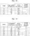
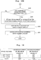
- the FPGA 72a selects a rank having the maximum number of nozzles and being not set with the aftermentioned flag (step S21). As depicted in Fig. 12 , for example, the rank C is selected, having the maximum number of nozzles 870 and being not set with the flag.
- the FPGA 72a calculates the quotient P of dividing the number of nozzles of the selected rank (870 of the rank C, for example) by the maximum number of drivable nozzles (560, for example) (step S22). The FPGA 72a determines whether the quotient P is equal to or less than one (step S23). If the quotient P is more than one (step S23: No), then the FPGA 72a determines whether the quotient P is more than one but is equal to or less than two (step S25).
- step S25 If the quotient P is more than one but is equal to or less than two (step S25: Yes), then the selected rank is divided by two and two power circuits are allocated respectively (step S26).
- the FPGA 72a sets the number of nozzles of each divided rank (the sub number of nozzles) to the half of the number of nozzles of the undivided rank. That is, the FPGA 72a divides the maximum number of nozzles and calculates the sub number of nozzles.
- the power circuit numbers of the allocated power circuits are stored in the table.
- the rank C is divided into a rank C1 and a rank C2, and a power circuit is allocated to each of the rank C1 and the rank C2.
- the number of nozzles of each of the divided rank C1 and rank C2 is the half of the number of nozzles 870 of the undivided rank C, that is, 435.
- the rank D is also divided into a rank D1 and a rank D2, and the number of nozzles of each of the divided ranks (the second sub number of nozzles) is the half of the number of nozzles 630 of the undivided rank, that is, 315. Then, two power circuits are allocated respectively. Further, the number of nozzles of the divided rank (the sub number of nozzles or the second sub number of nozzles) is not limited to the equally divided number of nozzles of the undividedrank.
- Each of the divided ranks is set with a flag indicating the allocation of the power circuit (step S28), and the number of allocated power circuits is subtracted from the number of remaining power circuits (step S29).
- the ranks C1 and C2 are set with the flags, and thus two is subtracted from the remaining power circuits.
- step S25 If the quotient P is more than two (step S25: No), that is, if the quotient P is larger than two, then the FPGA 72a divides the selected rank into three ranks, allocates three power circuits respectively to the same (step S26), and executes the step S28.
- the FPGA 72a determines whether the number of remaining power circuits is zero (step S30). If the number of remaining power circuits is not zero (step S30: No), then the FPGA 72a returns the process to the step S21. If the number of remaining power circuits is zero (step S30: Yes), then the FPGA 72a determines whether there is any rank without allocated power circuit (unallocated rank) (step S31).
- step S31 If there is any unallocated rank (step S31: Yes), then the FPGA 72a allocates, to the unallocated rank, the power circuit allocated to the rank having the closest drive voltage to the drive voltage of the unallocated rank (step S32).
- the FPGA 72a allocates, to the unallocated rank, the power circuit allocated to the rank having the closest drive voltage to the drive voltage of the unallocated rank (step S32).
- the FPGA 72a allocates, to the unallocated rank, the power circuit allocated to the rank having the closest drive voltage to the drive voltage of the unallocated rank (step S32).
- the rank A is an unallocated rank
- the fifth power circuit 25 which is already allocated to the rank B having the closest drive voltage to the drive voltage of the rank A, is allocated to the rank A.
- the drive voltage of the rank A is changed to the drive voltage of the rank B.
- the FPGA 72a sets the output voltages of the first power circuit 21 to the sixth power circuit 26 to correspond to the drive voltages of the nozzles 11 a corresponding to the ranks A to E (step S33).
- the FPGA 72a stores the nozzle addresses in the non-volatile memory 11e while associating each of the nozzle addresses with one of the first power circuit 21 to the sixth power circuit 26 (step S34), and then ends the process.
- step S23 if the quotient P is equal to or less than one (step S23: Yes), then the first power circuit 21 to the fifth power circuit 25 are allocated to the ranks A to D in descending order of the number of nozzles (step S24), and the process proceeds to the step S31.
- step S31 if there is no unallocated rank (step S31: No), then the FPGA 72a executes the step S33.
- the upper limit of the number of divided ranks is three in the steps S23 to S27, the upper limit may not be set.
- n may be sought within the range 1 ⁇ P ⁇ n (n is a natural number not smaller than two) to divide a rank by n.
- the upper limit of the dividing number is set as appropriate in consideration of the number of power circuits, the maximum number of drivable nozzles, the maximum number of nozzles among ranks, and the like.
- the maximum number of nozzles is divided to calculate the sub number of nozzles, and a plurality of small power circuits are allocated to the respective ranks in descending order of the number of nozzles and the sub number of nozzles. Further, the power circuit having the closest voltage to the voltage of an unallocated rank is allocated to the unallocated rank.
- At least two or more power circuits are allocated for supplying the power to the rank, where the number of nozzles (actuators) is equal to or larger than the predetermined number and the difference between the jetting amount of liquid droplets and its target value is more likely to be conspicuous.
- the number of nozzles (actuators) is equal to or larger than the predetermined number and the difference between the jetting amount of liquid droplets and its target value is more likely to be conspicuous.
- such ranks are defined as unallocated ranks that there is a small number of nozzles and the difference between the jetting amount of liquid droplets and its target value is less likely to be conspicuous.
- the second sub number of nozzles may be calculated and, in descending order of the number of nozzles, the sub number of nozzles and the second sub number of nozzles, a plurality of small power circuits may be allocated to the respective ranks. It is possible to minimize the number of the small power circuits in use, thereby suppressing the growing of the printing apparatus in size.
- the non-volatile memory 11e stores the maximum (predetermined) number of drivable nozzles for each of the first power circuit 21 to the sixth power circuit 26.
- the maximum number of drivable nozzles is 560 for each of the first power circuit 21 to the fifth power circuit 25.
- the non-volatile memory 11e stores the maximum number of power circuits allocatable to a single rank (the maximum allocation number), such as 2, for example.
- the non-volatile memory 11e stores the total number of power circuits (five in this embodiment) as the number of remaining power circuits.
- the number of nozzles in each of the ranks A to E is calculated in advance with a method including actual measurement.
- the calculated numbers of nozzles of the ranks A to E are stored in the non-volatile memory 11e.
- the numbers of nozzles of the ranks A to E are, respectively, 7, 150, 1200, 300, and 23.
- the power source number 6 is allocated preliminarily to the rank E of the highest drive voltage, and stored in the table.
- the FPGA 72a selects a rank (maximum rank) having the largest number of nozzles associated therewith and being not set with the aftermentioned flag from the ranks A to D (step S41). As depicted in Fig. 15 , for example, the rank C is selected, having the maximum number of nozzles 1200 and being not set with the flag.
- the FPGA 72a allocates a power circuit to the selected rank (step S42).
- the power circuit number of the allocated power circuit is stored in the table. As depicted in Fig. 16 , for example, the power source number 1 is stored for the rank C.
- the FPGA 72a subtracts the maximum number of drivable nozzles of the allocated power circuit from the number of nozzles of the rank to which the power circuit is allocated (step S43), and stores the subtracted result in the non-volatile memory 11e as the number of nozzles of that rank.
- the maximum number of drivable nozzles 560 of the first power circuit 21 is subtracted from the number of nozzles 1200 of the rank C, and stores the subtracted result 640 in the non-volatile memory 11e (see Fig. 16 ).
- the FPGA 72a decrements the number of remaining power circuits by one (step S44), and determines whether the number of power circuits allocated to the selected rank has reached the maximum allocation number (step S45). For example, it is determined whether the number of power circuits allocated to the rank C has reached two.
- step S45: No If it is determined that the number of the power circuits allocated to the selected rank has not reached the maximum allocation number (step S45: No), then the FPGA 72a determines whether the number of remaining power circuits is zero (step S47). If the number of remaining power circuits is not zero (step S47: No), then the FPGA 72a returns the process to the step S41.
- the process is returned to the step S41.
- the process is carried out from the step S41 with the number of nozzles 640 in the rank C. That is, the FPGA 72a carries out the process from the step S41 with the numbers of nozzles in the ranks A to D being, respectively, 7, 150, 640, and 300.
- step S45 If it is determined that the number of power circuits allocated to the selected rank has reached the maximum allocation number (step S45: Yes), then the FPGA 72a sets the selected rank with the flag indicating completion of allocating the power circuits (step S46), and carries out the step S47.
- the rank C is set with the flag. Thereafter, when the process is returned to the step S41, the rank C set with the flag will not be selected. That is, in the step S41, the FPGA 72a selects a rank having the maximum number of nozzles from the ranks A, B, and D.
- the FPGA 72a subtracts the maximum number of drivable nozzles 560 of the first power circuit 21 from the number of nozzles 640 of the rank C, and the subtracted result 80 is stored in the non-volatile memory 11e.
- step S47: Yes If the number of remaining power circuits is zero (step S47: Yes), then the FPGA 72a determines whether the subtracted number of nozzles exceeds zero in the rank set with the flag (step S48). If the subtracted number of nozzles exceeds zero (step S48: Yes), then the FPGA 72a divides the subtracted number of nozzles to allocate the same to another rank (step S49).
- the number of nozzles after the subtraction is 80, exceeding zero.
- the number of nozzles 80 after the subtraction is equally divided to allocate 40 to each of the rank B and the rank D having the closest drive voltage to the drive voltage of the rank C. That is, among the nozzles 11 a in the rank C, 40 nozzles 11 a are changed to the rank B while the other 40 nozzles 11 a are changed to the rank D.
- the number of nozzles of the rank C is changed from 1200 to 1120, the number of nozzles of the rank B is changed from 150 to 190, and the number of nozzles of the rank D is changed from 300 to 340.
- the difference between the drive voltage of the rank C and the drive voltage of each of the rank B and the rank D is set to be not higher than a predetermined value such as not higher than 1.0[V]. That is, the number of nozzles 80 after the subtraction in the rank C (rank of maximum number of nozzles) is allocated to the ranks B and D (other ranks) whose voltage differences from the drive voltage of the rank C are not higher than the predetermined value.
- the FPGA 72a sets the output voltages of the first power circuit 21 to the sixth power circuit 26 to correspond to the drive voltages of the nozzles 11 a in the ranks A to E (step S50).
- the FPGA 72a stores the nozzle addresses in the non-volatile memory 11e while associating each of the nozzle addresses with one of the first power circuit 21 to the sixth power circuit 26 (step S51), and then ends the process. Further, in the step S48, if the number of nozzles after the subtraction does not exceed zero (step S48: No), then the FPGA 72a executes the step S50.
- the power circuits not more than the maximum allocation number are allocated to the rank of maximum number of nozzles (the rank C, for example) while the power circuits less than the maximum allocation number are allocated to other ranks. If the number of nozzles in the rank of maximum number of nozzles exceeds the total number of maximum number of drivable nozzles (a predetermined number) of the allocated one or plurality of power circuits, then the same number of nozzles 11 a as the number of subtracting the total number from the number of nozzles in the rank of maximum number of nozzles are allocated to the other ranks whose voltage difference from the voltage of the power circuit corresponding to the rank of maximum number of nozzles is not higher than the predetermined value.
- the number of small power circuits in use is minimized to suppress the growing of the printing apparatus in size.
- the difference between the jetting amount of liquid droplets and its target value is made as less conspicuous as possible.
- by only using the minimum necessary number of the power circuits having a small allowable power it is possible to suppress the growing of the printing apparatus in size.
- a printing apparatus according to a fifth embodiment will be explained below.
- those identical or similar to the components of the first embodiment to the fourth embodiment are assigned with the same reference signs, and any detailed explanation therefor is omitted.
- X be the maximum number of drivable nozzles of the first power circuit 21 to the third power circuit 23
- the higher the drive voltage the smaller the maximum number of drivable nozzles for one power circuit. Therefore, in the fifth embodiment, according to the drive voltage, the maximum numbers of drivable nozzles of the first power circuit 21 to the sixth power circuit 26 are changed.
- the maximum numbers of drivable nozzles of the first power circuit 21 to the sixth power circuit 26 are not limited to satisfying the above relation between X and Y, and may be set appropriately according to the specification of the printing apparatus.
- the maximum number of drivable nozzles varies with not only the drive voltage but also the number of times of driving the nozzles 11 a per unit time (the drive frequency) or temperature and the like. Hence, the maximum number of drivable nozzles of the first power circuit 21 to the sixth power circuit 26 may be changed according to the drive frequency or the temperature and the like.
- a printing apparatus according to a sixth embodiment will be explained below.
- L be the maximum number of drivable nozzles (a predetermined number) of the first power circuit 21 to the third power circuit 23
- M be the maximum number of drivable nozzles of the fourth power circuit 24 to the sixth power circuit 26.
- M is smaller than L.
- the larger the maximum number of drivable nozzles the larger the heat of the power circuit.
- One of a group of the first power circuit 21 to the third power circuit 23 and another group of the fourth power circuit 24 to the sixth power circuit 26 constitutes a first number of power circuits, whereas the other constitutes a second number of power circuits.
- the first power circuit 21 and the second power circuit 22 are juxtaposed on one surface of a substrate 200 and the sixth power circuit 26 is arranged between the first power circuit 21 and the second power circuit 22.
- the fourth power circuit 24 and the fifth power circuit 25 are juxtaposed on the other surface of the substrate 200 and the third power circuit 23 is arranged between the fourth power circuit 24 and the fifth power circuit 25.
- the fifth power circuit 25, the third power circuit 23, and the fourth power circuit 24 are positioned respectively on the back sides of the first power circuit 21, the sixth power circuit 26, and the second power circuit 22.
- the first power circuit 21 to the sixth power circuit 26 may be arranged as depicted in a second example of power circuit arrangement of Fig. 20 . That is, the power circuits of the maximum number of drivable nozzles L (the first power circuit 21 to the third power circuit 23) and the power circuits of the maximum number of drivable nozzles M (the fourth power circuit 24 to the sixth power circuit 26) are arranged alternately on one surface of the substrate 200 in a staggered form.
- each nozzle address indicates the position of a row of the nozzles 11a in one direction orthogonal to the row direction.
- the first power circuit 21 and the third power circuit 23 are allocated such that the number of times (a consecutive number) of consecutively allocating the first power circuit 21 and the third power circuit 23 to those consecutive nozzle addresses may be equal to or less than a second predetermined number (two, for example) (see Fig. 21 ). That is, the first power circuit 21 and the third power circuit 23 are allocated to the consecutive rows of the nozzles 11 a such that the consecutive number of the first power circuit 21 and the third power circuit 23 may be equal to or less than the second predetermined number (see Fig. 22 ). The first power circuit 21 and the third power circuit 23 may be allocated alternately one after another to the nozzle addresses of the rank C, such that the first power circuit 21 and the third power circuit 23 are allocated inconsecutively to the rows of the plurality of nozzles 11a.
- the same power circuit is allocated consecutively to a plurality of rows up to a predetermined number or more, then in the case of switching to another power circuit of the same applying voltage, density variation is liable to occur in the switched places. For example, after allocating the first power circuit 21 to three or more rows, if the third power circuit 23 is allocated to three or more rows, then the density variation is liable to occur in the border between the rows of the allocated first power circuit 21 and the rows of the allocated third power circuit 23.
- the seventh embodiment if a plurality of power circuits of the same applying voltage are allocated to a plurality of rows of the nozzles 11a juxtaposed in one direction, then the plurality of power circuits of the same applying voltage are allocated to the plurality of rows such that either the identical power circuits are inconsecutive or the number of consecutive identical power circuits is equal to or less than a predetermined number (two, for example). By virtue of this, it is possible to suppress the density variation in the places of switching the power circuits in use.
- the density is averaged such that the density variation is less visible.
- a control program recorded in a recording medium 150 may be installed in the external device 9.
- the external device 9 includes a CPU (Central Processing Unit), a ROM, a RAM, a non-volatile memory, and the like. Based on the installed control program, the CPU of the external device 9 accesses the non-volatile memory 11e of the head unit 11 to acquire necessary data, and carries out the processes according to the first embodiment to the fifth embodiment or the seventh embodiment.
- the necessary data may be stored in the non-volatile memory of the external device 9 if the control program is installed.
- the FPGAs 71a and 72a are used. Instead of the FPGAs 71 a and 72a, however, a processor such as a CPU or the like may be used. Further, the FPGAs 72a of the second substrates 72 may not be provided. In this case, the FPGA 71a sets the output voltages of the first power circuit 21 to the sixth power circuit 26, outputs the gate signals to the first control wire 33(1) to the nth control wire 33(n), and carries out the control of switching the switching circuit 27.
- the connector 11d is configured to be removable. Therefore, it is possible to select the head units 11 where the non-volatile memories 11e have stored the specification of the second substrates 72 such as the data according to the output voltages of the power circuits and the number of the power circuits, and to connect the same to the second substrates 72.
Landscapes
- Ink Jet (AREA)
- Particle Formation And Scattering Control In Inkjet Printers (AREA)
Abstract
Description
- The present invention relates to a printing apparatus jetting ink from nozzles.
- When the same drive voltage is applied respectively to nozzles, the nozzles have different jetting amounts (jetting velocities) of liquid droplets according to the properties of the nozzles. Conventionally, therefore, such liquid droplet jet apparatuses have been proposed as to select an optimal drive voltage for each nozzle such that the jetting amounts of liquid droplets from the nozzles may be equalized (for example, see Japanese Patent Application Laid-open No.
2008-173910 - In order to select the optimal drive voltage, it is necessary to provide a plurality of power sources having different voltages.
- However, if there are many nozzles having the same optimal drive voltage, then a large amount of electric power has to be supplied by one power circuit corresponding to those nozzles. Hence, it is necessary to prepare a power circuit capable of supplying a large amount of electric power and, meanwhile, the size of the power circuit capable of supplying a large amount of electric power is also large.
- The present teaching is made in view of the above situation, and an object thereof is to provide a printing apparatus capable of providing a plurality of power circuits while downsizing the power circuits to restrain the apparatus from growing in size.
- According to a first aspect of the present teaching, there is provided a printing apparatus including: actuators configured to exert force to liquid; power circuits configured to apply voltages to the actuators; a switching circuit configured to switch connection destination of each of the actuators to any of the power circuits; and a controller configured to control driving of the actuators, wherein each of the actuators is associated with one of ranks which represent magnitudes of the applying voltages, and the controller is configured to allocate at least two of the power circuits to a maximum rank, of the ranks, having the largest number of actuators associated therewith.
- In the printing apparatus according to the first aspect of the present teaching, a plurality of power circuits can be provided while downsizing the power circuits to restrain the apparatus from growing in size.
- In the printing apparatus according to the first aspect of the present teaching, the power circuits may include a standby power circuit corresponding to a standby power source, and the controller may be configured to allocate the standby power circuit to the maximum rank.
- In the printing apparatus according to the first aspect of the present teaching, each of the power circuits may be configured to apply voltage to a predetermined number or less of actuators, and the controller may be configured to: whenever one power circuit among the power circuits is allocated to one rank among the ranks, for the one rank to which the one power circuit is allocated, calculate a second number of actuators by subtracting the predetermined number from the number of actuators before allocating the one power circuit; allocate the power circuits to the ranks in descending order of the number of actuators and the second number of actuators associated therewith; determine whether there is any unallocated rank without any power circuit, among the power circuits, allocated thereto, after each of the power circuits is allocated to any of the ranks; and based on determining that there is an unallocated rank, allocate, to the unallocated rank, one of the power circuits which has the closest voltage to the voltage of the unallocated rank.
- In the printing apparatus according to the first aspect of the present teaching, each of the power circuits may be configured to apply voltage to a predetermined number or less of the actuators, and the controller may be configured to: select the maximum rank; determine whether the number of actuators associated with the selected rank is not more than the predetermined number; based on determining that the number of actuators associated with the selected rank is not more than the predetermined number, allocate the power circuits to the ranks in descending order of the number of actuators associated therewith; based on determining that the number of actuators associated with the selected rank is more than the predetermined number, calculate a value of dividing the number of actuators associated with the selected rank by the predetermined number; divide the number of actuators associated with the selected rank by the value to calculate a sub number of actuators; allocate the power circuits to the ranks in descending order of the number of actuators and the sub number of actuators associated therewith; determine whether there is any unallocated rank without any power circuit, among the power circuits, allocated thereto, after each of the power circuits is allocated to any of the ranks; and based on determining that there is an unallocated rank, allocate, to the unallocated rank, one of the power circuits which has the closest voltage to the voltage of the unallocated rank.
- In the printing apparatus according to the first aspect of the present teaching, the controller may be configured to, after calculating the sub number of actuators, select another rank having the second largest number of actuators next to the selected rank.
- In the printing apparatus according to the first aspect of the present teaching, a maximum allocation number of the power circuits allocatable to each of the ranks may be preset, each of the power circuits may be configured to apply voltage to a predetermined number or less of the actuators, and the controller may be configured to: whenever one power circuit among the power circuits is allocated to one rank among the ranks, for the one rank to which the one power circuit is allocated, calculate a second number of actuators by subtracting the predetermined number from the number of actuators before allocating the one power circuit; allocate a number of power circuits not more than the maximum allocation number to the maximum rank, and allocate a number of the power circuits less than the maximum allocation number to each of the other ranks; determine whether the number of actuators associated with the maximum rank is more than the total number of the predetermined numbers of all of the power circuits allocated to the maximum rank; based on determining that the number of actuators associated with the maximum rank is more than the total number of the predetermined numbers of all of the power circuits allocated to the maximum rank, calculate a value by subtracting the total number of the predetermined numbers from the number of actuators associated with the maximum rank; and allocate the same number as the calculated value of actuators associated with the maximum rank to the other ranks whose voltage difference from the voltage of the power circuit allocated to the maximum rank is not more than a predetermined value.
- In the printing apparatus according to the first aspect of the present teaching, the controller may be configured to: divide the same number as the value of actuators associated with the maximum rank; and allocate the divided actuators respectively to the other ranks.
- In the printing apparatus according to the first aspect of the present teaching, the predetermined number may be set according to a property of each of the power circuits, a drive voltage for each of the actuators, the number of actuators, a drive frequency of each of the actuators, or a temperature.
- In the printing apparatus according to the first aspect of the present teaching, the power circuits may include at least one first power circuit where the predetermined number is a first number, and at least one second power circuit where the predetermined number is a second number different from the first number, and one of the second power circuits may be arranged between two of the first power circuits or one of the first power circuits may be arranged between two of the second power circuits.
- In the printing apparatus according to the first aspect of the present teaching, the actuators may form a plurality of rows arranged in one direction, and under a condition that, among the plurality of rows, there are multiple rows belonging to one rank among the ranks and being consecutive in the one direction, and under a condition that one power circuit among the power circuits is allocated to the one rank, the controller may be configured to allocate the power circuits to the plurality of rows such that the one power circuit is not consecutive or the number of the one power circuit consecutive in the one direction is not more than a predetermined number.
- According to a second aspect of the present teaching, there is provided a printing apparatus including: actuators configured to exert force to liquid; power circuits configured to apply voltages to the actuators; and a switching circuit configured to switch connection destination of each of the actuators to any of the power circuits, wherein the actuators are divided into actuator groups according to the voltage of driving each of the actuators, and at least two of the power circuits are connected to an actuator group, of the actuator groups, having the largest number of actuators included therein, by the switching circuit.
- In the printing apparatus according to the second aspect of the present teaching, it is possible to minimize the number of the power circuits in use for the printing apparatus and thus restrain the apparatus from growing in size.
-
-
Fig. 1 is a plan view schematically depicting a printing apparatus according to a first embodiment of the present teaching. -
Fig. 2 is a schematic cross-sectional view taken along the line II-II depicted inFig. 1 . -
Fig. 3 is a bottom plan view of an ink-jet head. -
Fig. 4 is a block diagram schematically depicting connection of a controller and head units. -
Fig. 5 is a block diagram schematically depicting a configuration in the vicinity of a power source. -
Fig. 6 is a circuit diagram schematically depicting a configuration of a CMOS (Complementary Metal-Oxide-Semiconductor) circuit to drive nozzles. -
Fig. 7 is a graph depicting a relationship between a nozzle address identifying each nozzle and a velocity of liquid droplets (ink) jetted from each nozzle corresponding to the nozzle address when a certain voltage is applied to piezoelectric bodies. -
Fig. 8 is a conceptual diagram depicting an example of allocation table for power circuits. -
Fig. 9 is a flowchart explaining a power circuit allocation process. -
Fig. 10 is a conceptual diagram depicting an example of allocation table for power circuits in a printing apparatus according to a second embodiment. -
Fig. 11 is a flowchart explaining a power circuit allocation process in the second embodiment. -
Fig. 12 is a conceptual diagram depicting an example of allocation table for power circuits before allocating the power circuits in a printing apparatus according to a third embodiment. -
Fig. 13 is a conceptual diagram depicting an example of allocation table for the power circuits after allocating the power circuits in the third embodiment. -
Figs. 14A and14B depict a flowchart explaining a power circuit allocation process in the third embodiment. -
Fig. 15 is a conceptual diagram depicting an example of allocation table for power circuits before allocating the power circuits in a printing apparatus according to a fourth embodiment. -
Fig. 16 is a conceptual diagram depicting an example of allocation table for the power circuits in the course of allocating the power circuits in the fourth embodiment. -
Fig. 17 is a conceptual diagram depicting an example of allocation table for the power circuits after allocating the power circuits in the fourth embodiment. -
Figs. 18A and18B depict a flowchart explaining a power circuit allocation process in the fourth embodiment. -
Fig. 19 is a table depicting a relationship between the maximum number of driven nozzles and the drive voltage of a power circuit in a printing apparatus according to a fifth embodiment. -
Fig. 20 is an explanatory diagram explaining an arrangement of power circuits in a printing apparatus according to a sixth embodiment. -
Fig. 21 is a table depicting an example of relationship between a nozzle address, rank, and power source number in a printing apparatus according to a seventh embodiment. -
Fig. 22 is an explanatory diagram explaining the power source number and an arrangement of nozzles driven by a plurality of power circuits having the same drive voltage. - Referring to
Figs. 1 to 9 , a printing apparatus according to a first embodiment will be explained below. - In
Fig. 1 , the front side of aprinting apparatus 1 is defined on the downstream side in a conveyance direction ofrecording paper 100, whereas the rear side of theprinting apparatus 1 is defined on the upstream side in the conveyance direction. Further, the left-right direction of theprinting apparatus 1 is defined in such a direction along the paper width as is parallel to the conveyance plane of the recording paper 100 (the plane parallel to the page ofFig. 1 ) and is orthogonal to the conveyance direction. Further, the left side ofFig. 1 is the left side of theprinting apparatus 1 whereas the right side ofFig. 1 is the right side of theprinting apparatus 1. Further, the upper-lower or vertical direction of theprinting apparatus 1 is defined in a direction orthogonal to the conveyance plane of the recording paper 100 (a direction orthogonal to the page ofFig. 1 ). InFig. 1 , the front or near side of the page is the upper side whereas the rear side or far side of the page is the lower side. Those defined front, rear, left, right, upper, and lower will be used appropriately in the following explanation. - As depicted in
Fig. 1 , theprinting apparatus 1 includes acasing 2, aplaten 3, four ink-jet heads 4, twoconveyance rollers controller 7. - The
platen 3 is placed horizontally in thecasing 2. Therecording paper 100 is placed on the upper surface of theplaten 3. The four ink-jet heads 4 are provided above theplaten 3 to be juxtaposed in the front-rear direction. The twoconveyance rollers platen 3. The twoconveyance rollers recording paper 100 on theplaten 3 to the front side. - The
controller 7 includes non-volatile memories and the like such as a plurality ofFPGAs Fig. 4 ), a ROM (Read Only Memory), a RAM (Random Access Memory), and an EEPROM (Electrically Erasable Programmable Read-Only Memory). Further, illustration of the ROM, RAM, EEPROM and the like is omitted here. Further, thecontroller 7 is connected with anexternal device 9 such as a PC or the like in a data communicable manner, to control each device of theprinting apparatus 1 based on print data sent from theexternal device 9. - For example, the
controller 7 controls the motor for driving theconveyance rollers conveyance rollers recording paper 100 in the conveyance direction. Further, thecontroller 7 controls the ink-jet heads 4 to jet inks toward therecording paper 100. By virtue of this, image is printed on therecording paper 100. -
Head holders 8 are installed in thecasing 2. Thehead holders 8 are arranged above theplaten 3 and juxtaposed in the front-rear direction between theconveyance rollers head holders 8 hold the ink-jet heads 4 respectively. - The four ink-
jet heads 4 respectively jet the inks of four colors: cyan (C), magenta (M), yellow (y), and black (K). Each of the ink-jet heads 4 is supplied with the ink of the corresponding color from an undepicted ink tank. - As depicted in
Figs. 2 and3 , each of the ink-jet heads 4 includes aholder 10 in a rectangular plate-like shape elongated in the paper width direction, andhead units 11 attached to theholder 10. - A plurality of
nozzles 11a (actuators) are formed on the lower surface of each of thehead units 11. Each of thenozzles 11 a includes an aftermentionedpiezoelectric body 11b (seeFig. 6 ). The plurality ofnozzles 11a of each of thehead units 11 are juxtaposed along the paper width direction which is the longitudinal direction of the ink-jet heads 4, and thehead units 11 form afirst head row 81 and asecond head row 82. Thefirst head row 81 and thesecond head row 82 are juxtaposed in the conveyance direction and thefirst head row 81 is positioned on the rear side of thesecond head row 82. - As depicted in
Fig. 3 , a left end portion of eachhead unit 11 in thefirst head row 81 is at the same position as a right end portion of onehead unit 11 in thesecond head row 82 in the left-right direction. In other words, the left end portion of eachhead unit 11 in thefirst head row 81 overlaps with the right end portion of onehead unit 11 in thesecond head row 82 in the front-rear direction. - As depicted in
Fig. 2 , theholder 10 is provided with aslit 10a. Aflexible substrate 51 connects thehead units 11 and thecontroller 7, and theflexible substrate 51 is inserted through theslit 10a. - The
head units 11 are arranged along an arrangement direction which is the paper width direction. Thehead units 11 are arranged to be alternately separate between the front side and the rear side in the conveyance direction. Between thehead units 11 arranged on the front side and thehead units 11 arranged on the rear side, there is a positional deviation on the left and the right (in the arrangement direction). In this embodiment, thehead units 11 are juxtaposed along the direction orthogonal to the conveyance direction (along the paper width direction). However, thehead units 11 may be arranged obliquely, that is, along a direction intersecting the conveyance direction at an angle other than 90 degrees. - As depicted in
Figs. 1 and2 , areservoir 12 is provided above thehead units 11. An illustration of thereservoir 12 is omitted inFig. 3 . - The
reservoir 12 is connected to one of the ink tanks (not depicted) via atube 16 to temporarily retain the ink supplied from the ink tank. Thereservoir 12 has a lower portion connected to thehead units 11 to supply each of thehead units 11 with the ink from thereservoir 12. Further, thehead units 11 may be moved in the paper width direction. - As depicted in
Fig. 4 , thecontroller 7 includes afirst substrate 71 and a plurality ofsecond substrates 72. Thefirst substrate 71 is provided with theFPGA 71a. Onesecond substrate 72 is provided with oneFPGA 72a. TheFPGA 71 a is connected to theFPGAs 72a to control the driving of theFPGAs 72a. Thesecond substrates 72, that is, theFPGAs 72a correspond respectively to the plurality ofhead units 11, and the number of theFPGAs 72a is the same as the number ofhead units 11. TheFPGAs 72a are connected respectively with thehead units 11. TheFPGA 71a and theFPGAs 72a are connected to the ROM (not depicted) storing bit stream information and to the RAM (not depicted) as a memory. - Each of the
head units 11 includes asubstrate 11c on which aremovable connector 11 d, anon-volatile memory 11e, and adriver IC 11f are mounted. Each of thehead units 11 is connected to one of thesecond substrates 72 in a removable manner via theconnector 11d. Each of thedriver ICs 11f includes a switchingcircuit 27 which will be described later on. - As depicted in
Fig. 5 , thesecond substrate 72 is provided with a D/A (Digital/Analog)converter 20. Further, thesecond substrate 72 is provided with a plurality of power circuits and, particularly in this embodiment, is provide with afirst power circuit 21 to asixth power circuit 26. Each of thefirst power circuit 21 to thesixth power circuit 26 has an FET, impedance and the like, and output voltage thereof is changeable. As thosefirst power circuit 21 tosixth power circuit 26, for example, switching-type DC/DC converters may be adopted. TheFPGA 72a outputs a signal to thefirst power circuit 21 to thesixth power circuit 26 via the D/A converter 20, to set the output voltage. - The
first power circuit 21 to thesixth power circuit 26 are connected to a first power wire 34(1) to an nth power wire 34(n) (n is a natural number not smaller than two) via the switchingcircuit 27. The switchingcircuit 27 connects each of the first power wire 34(1) to the nth power wire 34(n) to any of thefirst power circuit 21 to thesixth power circuit 26. Thefirst power circuit 21 to thefourth power circuit 24 are ordinary power circuits which are ordinary used. Thefifth power circuit 25 may be an ordinary power circuit or a standby power circuit while thesixth power circuit 26 is a power circuit of special specification. Thesixth power circuit 26 is, for example, used for the highest rank of the drive voltages, or used concurrently as a power supply voltage for the VCOM of the actuators, or used for thenozzles 11a jetting the inks less easily, or used as an HVDD (the back gate voltage on the high side) of aPMOS transistor 31. - The HVDD voltage is connected to the
sixth power circuit 26 whose output voltage is higher than thefirst power circuit 21 to thefifth power circuit 25 such that no electric current may flow in any parasitic diode of thePMOS transistor 31 on the high side even if a higher voltage is applied to adrain terminal 31b than to a source terminal 31a of thePMOS transistor 31. - As depicted in
Fig. 6 , theprinting apparatus 1 is provided with a plurality ofCMOS circuits 30 to respectively drive thenozzles 11a. TheFPGAs 72a output gate signals to theCMOS circuits 30 via a first control wire 33(1) to an nth control wire 33(n) (n is a natural number not smaller than two). Further, the first control wire 33(1) to the nth control wire 33(n) correspond to the first power wire 34(1) to the nth power wire 34(n). That is, the first control wire 33(1) corresponds to the first power wire 34(1), and the nth control wire 33(n) corresponds to the nth power wire 34(n). - The
FPGA 72a outputs a signal to the switchingcircuit 27 to connect each of the first power wire 34(1) to the nth power wire 34(n) to any of thefirst power circuit 21 to thesixth power circuit 26. TheFPGA 72a accesses thenon-volatile memory 11e as necessary. Thenon-volatile memory 11e stores a plurality of nozzle addresses identifying therespective nozzles 11 a, ranks corresponding to the nozzle addresses, and the like. The ranks will be described later on. - As depicted in
Fig. 6 , theCMOS circuit 30 includes the PMOS (P-type Metal-Oxide-Semiconductor)transistor 31, an NMOS (N-type Metal-Oxide-Semiconductor)transistor 32, animpedance 35, twopiezoelectric bodies piezoelectric bodies piezoelectric body 11b may be provided. The source terminal 31a of thePMOS transistor 31 is connected to any of the first power wire 34(1) to the nth power wire 34(n). Asource terminal 32a of theNMOS transistor 32 is grounded. - The
drain terminals PMOS transistor 31 andNMOS transistor 32 are connected to one end of theimpedance 35. The other end of theimpedance 35 is connected to the other end of thepiezoelectric body 11b' on one hand and to one end of thepiezoelectric body 11b on the other hand. The one end of thepiezoelectric body 11b' on the one hand is connected to the VCOM voltage, that is, the sixth power supply voltage, whereas the other end of thepiezoelectric body 11b on the other hand is grounded. - The
PMOS transistor 31 andNMOS transistor 32 havegate terminals PMOS transistor 31. - If an output signal "L" is inputted from the
FPGA 72a to thegate terminals PMOS transistor 31 andNMOS transistor 32, then thePMOS transistor 31 is conducted, thepiezoelectric body 11b is charged, and thepiezoelectric body 11b' is discharged. If an output signal "H" is inputted from theFPGA 72a to thegate terminals PMOS transistor 31 andNMOS transistor 32, then theNMOS transistor 32 is conducted, thepiezoelectric body 11b is discharged, and thepiezoelectric body 11b' is charged. Charging and discharging thepiezoelectric bodies piezoelectric bodies nozzle 11a. - The ranks of the
nozzles 11a will be explained.Fig. 7 is a graph depicting a relationship between a nozzle address identifying each nozzle and a velocity of liquid droplets (ink) jetted from eachnozzle 11a corresponding to the nozzle address when a certain voltage is applied to thepiezoelectric bodies - As depicted in
Fig. 7 , for example, the liquid droplet velocity is set in five velocity ranges to correspond to the rank A to the rank E, respectively. Further, the rank A corresponds to the highest velocity range whereas the rank E corresponds to the lowest velocity range. Thenon-volatile memory 11e stores the rank A to the rank E according to the liquid droplet velocity of eachnozzle 11a, and the corresponding respective nozzle addresses. While the liquid droplet velocity is taken as an example here, it is possible to use the same concept for the jetting amount of liquid droplets. - The
non-volatile memory 11e of thehead unit 11 stores such an allocation table as inFig. 8 , indicating an allocation of power circuits to thenozzles 11a. InFig. 8 , the column of the number of nozzles depicts the number of thenozzles 11a corresponding to the respective ranks, being preset in thenon-volatile memory 11e according to each rank. The column of power source number depicts the power circuit number allocated to each rank. The column of drive voltage depicts the voltage for driving thenozzles 11a corresponding to each rank. In other words, the rank represents the magnitude of the voltage applied to thenozzles 11a. - The drive voltage serves for jetting the inks from the
nozzles 11a at the targeted liquid droplet velocity, and is preset in thenon-volatile memory 11e for each rank to suppress the difference in the liquid droplet velocity between thenozzles 11a. Further, thepower source numbers 1 to 6 correspond respectively to thefirst power circuit 21 to thesixth power circuit 26. - The number of nozzles in each of the ranks A to E is calculated in advance with a method including actual measurement. The calculated number of nozzles is stored in a table in the
non-volatile memory 11e. For example, as depicted inFig. 8 , the number of nozzles included in the ranks A to E are, respectively, 10, 350, 800, 500, and 20. - First, the
power source number 6 is allocated to the rank E of the highest drive voltage. Further, in descending order of the number of nozzles, the ordinary power circuits, that is, thefirst power circuit 21 to thefourth power circuit 24, are allocated respectively to the ranks A to D. The power circuit number of the allocated power circuit is stored in the table. For example, as depicted inFig. 8 , thepower source numbers - The
FPGA 72a allocates the standby power circuit, that is, thefifth power circuit 25, to the rank having the maximum number of nozzles (step S1 inFig. 9 ). The power circuit number of the allocated standby power circuit is stored in the table. For example, as depicted inFig. 8 , thepower source number 5 is allocated in the rank C. - The
FPGA 72a sets the output voltages of thefirst power circuit 21 to thesixth power circuit 26 to correspond to the drive voltages of thenozzles 11 a corresponding to the ranks A to E (step S2 inFig. 9 ). TheFPGA 72a stores the nozzle addresses in thenon-volatile memory 11e while associating each of the nozzle addresses with one of thefirst power circuit 21 to the sixth power circuit 26 (step S3 inFig. 9 ), and then ends the process. The step S1 corresponds to the power circuit allocation process. - With respect to the printing apparatus according to the first embodiment, it is possible to appropriately allocate the
first power circuit 21 to thesixth power circuit 26 to the respective ranks A to E so as to minimize the number of small power circuits in use and thus restrain the apparatus from growing in size. Further, by allocating the standby power circuit to the rank having the maximum number of nozzles, it is possible to minimize the number of the power circuits in use and thus restrain the apparatus from growing in size without adding ordinary power circuits. - In the first embodiment, at least two power circuits are allocated to supply the power to the rank associated with a large number of nozzles (actuators) and the difference between the jetting amount of liquid droplets and its target value is more likely to be conspicuous. Therefore, it is possible to secure a certain number or more of the ranks (four ranks or more in the first embodiment) of the drive voltages needed to adjust the variation of the nozzles in the jetting amount of liquid droplets. Further, the power circuits in use only have a small allowable power. The maximum number of nozzles which can be driven by the power circuits in use is 1/2 or less (1/3 in the first embodiment) of the number of all nozzles of the
head unit 11. That is, the apparatus is restrained from growing in size by securing a certain number of the ranks for the necessary drive voltages while only using the minimum number of the required power circuits only having the small allowable power. - Without using any power circuits having a large allowable power capable of driving all the nozzles (actuators) included in the rank having the maximum number of nozzles, the standby power circuit is allocated to the rank, which has the maximum number of nozzles and in which the difference between the jetting amount of liquid droplets and its target value is more likely to be conspicuous. Therefore, it is possible to restrain the apparatus from growing in size by only using the power circuits having the small allowable power. A power circuit having a large allowable power needs to have not only large switching elements (MOSFET, for example), inductors, condensers, heat dissipation patterns for lost heat, and the like, but also a wide wiring range. As a result, the power circuit with the large allowable power grows in size, thereby causing the entire printing apparatus to grow in size if the power circuit with the large allowable power is used.
- Referring to
Figs. 10 and11 , a printing apparatus according to a second embodiment will be explained below. Further, among the components according to the second embodiment, those identical or similar to the components of the first embodiment are assigned with the same reference signs, and any detailed explanation therefor is omitted. Thenon-volatile memory 11e stores the maximum number of the drivable nozzles with respect to each of thefirst power circuit 21 to thefifth power circuit 25. For example, the maximum number of the drivable nozzles for thefirst power circuit 21 to thefifth power circuit 25 is 560. Further, in the initial state, thenon-volatile memory 11e stores the total number of the power circuits (5 in the second embodiment) as the number of remaining power circuits. - The number of nozzles in each of the ranks A to E is calculated in advance with a method including actual measurement. The calculated number of nozzles is stored in the table in the
non-volatile memory 11e. For example, as depicted inFig. 10 , the numbers of nozzles included in the ranks A to E are, respectively, 5, 150, 870, 630, and 25. Further, thepower source number 6 is allocated preliminarily to the rank E of the highest drive voltage, and stored in the table. - The
FPGA 72a allocates an unallocated power circuit to the rank having the maximum number of nozzles among the ranks A to D (step S11). The power circuit number of the allocated power circuit is stored in the table. As depicted inFig. 10 , for example, thepower source number 1 is allocated to the rank C. TheFPGA 72a subtracts the maximum number of drivable nozzles of the allocated power circuit from the number of nozzles of the rank of the allocated power circuit (step S12). TheFPGA 72a stores the number of nozzles after the subtraction in thenon-volatile memory 11e as the number of nozzles of the rank of the allocated power circuit. As depicted inFig. 10 , for example, the maximum number ofdrivable nozzles 560 is subtracted from the number ofnozzles 870 of the rank C, and the number 310 is stored as the number of the nozzles of the rank C. Further, the maximum number ofdrivable nozzles 560 is subtracted from the number ofnozzles 630 of the rank D, and the number 70 is stored as the number of nozzles of the rank D. - The
FPGA 72a decrements the number of remaining power circuits by one (step S13), and then determines whether the number of remaining power circuits is zero (step S14). If the number of remaining power circuits is not zero (step S14: No), then theFPGA 72a returns the process to the step S11. In the process of thestep S 11, the power circuit already allocated to a rank will not be allocated to any other rank. By virtue of this, the power circuits are allocated one by one to the respective ranks in descending order of the number of nozzles. - If the number of the remaining power circuits is zero (step S14: Yes), then the
FPGA 72a determines whether there is any rank to which no power circuit is allocated (unallocated rank) (step S 15). If there is any unallocated rank (step S 15: Yes), then such a power circuit is allocated to the unallocated rank as having the closest drive voltage to the drive voltage of the unallocated rank (step S16). As depicted inFig. 10 , for example, if the rank A is an unallocated rank, then thefourth power circuit 24, which was allocated to the rank B, is allocated to the rank A because thefourth power circuit 24 has the closest drive voltage to the drive voltage of the rank A (step S16). In other words, the drive voltage for thenozzles 11 a in the rank A is changed to the drive voltage for thenozzles 11 a in the rank B. - The
FPGA 72a sets the output voltages of thefirst power circuit 21 to thesixth power circuit 26 to correspond to the drive voltages of thenozzles 11 a in the ranks A to E (step S17). TheFPGA 72a stores the nozzle addresses in thenon-volatile memory 11e while associating each of the nozzle addresses with one of thefirst power circuit 21 to the sixth power circuit 26 (step S18), and then ends the process. If there is no unallocated rank (step S 15: No), then theFPGA 72a executes the step S 17. - With respect to the printing apparatus according to the second embodiment, a plurality of small power circuits are allocated to the respective ranks in descending order of the number of nozzles. If there is any unallocated rank, then the power circuit having the closest drive voltage to the drive voltage of the unallocated rank is allocated to the unallocated rank, thereby minimizing the number of the small power circuits in use so as to suppress the growing of the printing apparatus in size.
- By allocating a plurality of power circuits to the respective ranks in descending order of the number of nozzles, it is possible to allocate at least two or more power circuits to the rank, where the number of nozzles (actuators) is larger than or equal to a predetermined number and the difference between the jetting amount of liquid droplets and its target value is more likely to be conspicuous. On the other hand, if it is not possible to allocate the power circuits to all ranks, then such ranks are defined as unallocated ranks that there is a small number of nozzles and the difference between the jetting amount of liquid droplets and its target value is less likely to be conspicuous. It is possible to secure a certain number or more of the ranks (four ranks or more in this embodiment) of the drive voltages needed to adjust the variation of the jetting amount of liquid droplets of each nozzle by allocating the power circuit having the closest voltage to voltage of the unallocated rank to the unallocated rank. Further, by only using the minimum necessary number of the power circuits having the small allowable power, it is possible to suppress the growing of the printing apparatus in size.
- Referring to
Figs. 12 to 14B , a printing apparatus according to a third embodiment will be explained below. Among the components according to the third embodiment, those identical or similar to the components of the first embodiment or the second embodiment are assigned with the same reference signs, and any detailed explanation therefor is omitted. In the initial state, all of the ranks are not set with aftermentioned flags. Further, in the initial state, thenon-volatile memory 11e stores the total number of the power circuits (five in this embodiment) as the number of the remaining power circuits. - The number of nozzles in each of the ranks A to E is calculated in advance with a method including actual measurement. The calculated number of nozzles is stored in a table in the
non-volatile memory 11e. For example, as depicted inFig. 12 , the numbers of nozzles of the ranks A to E are, respectively, 5, 150, 870, 630, and 25. Further, thepower source number 6 is allocated preliminarily to the rank E of the highest drive voltage, and stored in the table. - From the ranks A to D, the
FPGA 72a selects a rank having the maximum number of nozzles and being not set with the aftermentioned flag (step S21). As depicted inFig. 12 , for example, the rank C is selected, having the maximum number ofnozzles 870 and being not set with the flag. - The
FPGA 72a calculates the quotient P of dividing the number of nozzles of the selected rank (870 of the rank C, for example) by the maximum number of drivable nozzles (560, for example) (step S22). TheFPGA 72a determines whether the quotient P is equal to or less than one (step S23). If the quotient P is more than one (step S23: No), then theFPGA 72a determines whether the quotient P is more than one but is equal to or less than two (step S25). - If the quotient P is more than one but is equal to or less than two (step S25: Yes), then the selected rank is divided by two and two power circuits are allocated respectively (step S26). The
FPGA 72a sets the number of nozzles of each divided rank (the sub number of nozzles) to the half of the number of nozzles of the undivided rank. That is, theFPGA 72a divides the maximum number of nozzles and calculates the sub number of nozzles. The power circuit numbers of the allocated power circuits are stored in the table. - As depicted in
Fig. 13 , for example, because the quotient of dividing the number ofnozzles 870 of the rank C by the maximum number ofdrivable nozzles 560 is about 1.55, the rank C is divided into a rank C1 and a rank C2, and a power circuit is allocated to each of the rank C1 and the rank C2. The number of nozzles of each of the divided rank C1 and rank C2 is the half of the number ofnozzles 870 of the undivided rank C, that is, 435. - Likewise, the rank D is also divided into a rank D1 and a rank D2, and the number of nozzles of each of the divided ranks (the second sub number of nozzles) is the half of the number of
nozzles 630 of the undivided rank, that is, 315. Then, two power circuits are allocated respectively. Further, the number of nozzles of the divided rank (the sub number of nozzles or the second sub number of nozzles) is not limited to the equally divided number of nozzles of the undividedrank. - Each of the divided ranks is set with a flag indicating the allocation of the power circuit (step S28), and the number of allocated power circuits is subtracted from the number of remaining power circuits (step S29). For example, the ranks C1 and C2 are set with the flags, and thus two is subtracted from the remaining power circuits.
- If the quotient P is more than two (step S25: No), that is, if the quotient P is larger than two, then the
FPGA 72a divides the selected rank into three ranks, allocates three power circuits respectively to the same (step S26), and executes the step S28. - The
FPGA 72a determines whether the number of remaining power circuits is zero (step S30). If the number of remaining power circuits is not zero (step S30: No), then theFPGA 72a returns the process to the step S21. If the number of remaining power circuits is zero (step S30: Yes), then theFPGA 72a determines whether there is any rank without allocated power circuit (unallocated rank) (step S31). - If there is any unallocated rank (step S31: Yes), then the
FPGA 72a allocates, to the unallocated rank, the power circuit allocated to the rank having the closest drive voltage to the drive voltage of the unallocated rank (step S32). As depicted inFig. 13 , for example, if the rank A is an unallocated rank, then thefifth power circuit 25, which is already allocated to the rank B having the closest drive voltage to the drive voltage of the rank A, is allocated to the rank A. In other words, the drive voltage of the rank A is changed to the drive voltage of the rank B. - The
FPGA 72a sets the output voltages of thefirst power circuit 21 to thesixth power circuit 26 to correspond to the drive voltages of thenozzles 11 a corresponding to the ranks A to E (step S33). TheFPGA 72a , stores the nozzle addresses in thenon-volatile memory 11e while associating each of the nozzle addresses with one of thefirst power circuit 21 to the sixth power circuit 26 (step S34), and then ends the process. - In the step S23, if the quotient P is equal to or less than one (step S23: Yes), then the
first power circuit 21 to thefifth power circuit 25 are allocated to the ranks A to D in descending order of the number of nozzles (step S24), and the process proceeds to the step S31. - In the step S31, if there is no unallocated rank (step S31: No), then the
FPGA 72a executes the step S33. - In the third embodiment, although the upper limit of the number of divided ranks is three in the steps S23 to S27, the upper limit may not be set. For example, n may be sought within the
range 1 < P ≦ n (n is a natural number not smaller than two) to divide a rank by n. The upper limit of the dividing number is set as appropriate in consideration of the number of power circuits, the maximum number of drivable nozzles, the maximum number of nozzles among ranks, and the like. - With respect to the printing apparatus according to the third embodiment, the maximum number of nozzles is divided to calculate the sub number of nozzles, and a plurality of small power circuits are allocated to the respective ranks in descending order of the number of nozzles and the sub number of nozzles. Further, the power circuit having the closest voltage to the voltage of an unallocated rank is allocated to the unallocated rank. By virtue of this, it is possible to minimize the number of the small power circuits in use so as to suppress the growing of the printing apparatus in size.
- By allocating, to the unallocated rank, the power circuit having the closest voltage to the voltage of the unallocated rank, at least two or more power circuits are allocated for supplying the power to the rank, where the number of nozzles (actuators) is equal to or larger than the predetermined number and the difference between the jetting amount of liquid droplets and its target value is more likely to be conspicuous. On the other hand, if it is not possible to allocate power circuits to all ranks, then such ranks are defined as unallocated ranks that there is a small number of nozzles and the difference between the jetting amount of liquid droplets and its target value is less likely to be conspicuous. It is possible to secure a certain number or more of the ranks (four ranks or more in this embodiment) of the drive voltages needed to adjust the variation of the jetting amount of liquid droplets of each nozzle by allocating, to the unallocated rank, the power circuit having the closest voltage to voltage of the unallocated rank. Further, by only using the minimum necessary number of the power circuits having a small allowable power, it is possible to suppress the growing of the printing apparatus in size.
- As necessary, for the next largest number of nozzles to the maximum number of nozzles, the second sub number of nozzles may be calculated and, in descending order of the number of nozzles, the sub number of nozzles and the second sub number of nozzles, a plurality of small power circuits may be allocated to the respective ranks. It is possible to minimize the number of the small power circuits in use, thereby suppressing the growing of the printing apparatus in size.
- By allocating a plurality of power circuits to the respective ranks in descending order of the number of nozzles, sub number of nozzles and second sub number of nozzles, it is possible to allocate at least two or more power circuits for supplying the power to all of the ranks, where the number of nozzles (actuators) is equal to or larger than a predetermined number and the difference between the jetting amount of liquid droplets and its target value there is more likely to be conspicuous. Thus, by only using the power circuits having a small allowable power, it is possible to suppress the growing of the printing apparatus in size.
- Referring to
Figs. 15 to 18B , a printing apparatus according to a fourth embodiment will be explained below. Among the components according to the fourth embodiment, those identical or similar to the components of the first embodiment to the third embodiment are assigned with the same reference signs, and any detailed explanation therefor is omitted. Thenon-volatile memory 11e stores the maximum (predetermined) number of drivable nozzles for each of thefirst power circuit 21 to thesixth power circuit 26. For example, the maximum number of drivable nozzles is 560 for each of thefirst power circuit 21 to thefifth power circuit 25. Further, thenon-volatile memory 11e stores the maximum number of power circuits allocatable to a single rank (the maximum allocation number), such as 2, for example. - In the initial state, all of the ranks are not set with the aftermentioned flags. Further, in the initial state, the
non-volatile memory 11e stores the total number of power circuits (five in this embodiment) as the number of remaining power circuits. - The number of nozzles in each of the ranks A to E is calculated in advance with a method including actual measurement. The calculated numbers of nozzles of the ranks A to E are stored in the
non-volatile memory 11e. For example, as depicted inFig. 15 , the numbers of nozzles of the ranks A to E are, respectively, 7, 150, 1200, 300, and 23. Further, thepower source number 6 is allocated preliminarily to the rank E of the highest drive voltage, and stored in the table. - The
FPGA 72a selects a rank (maximum rank) having the largest number of nozzles associated therewith and being not set with the aftermentioned flag from the ranks A to D (step S41). As depicted inFig. 15 , for example, the rank C is selected, having the maximum number ofnozzles 1200 and being not set with the flag. - The
FPGA 72a allocates a power circuit to the selected rank (step S42). The power circuit number of the allocated power circuit is stored in the table. As depicted inFig. 16 , for example, thepower source number 1 is stored for the rank C. TheFPGA 72a subtracts the maximum number of drivable nozzles of the allocated power circuit from the number of nozzles of the rank to which the power circuit is allocated (step S43), and stores the subtracted result in thenon-volatile memory 11e as the number of nozzles of that rank. - For example, the maximum number of
drivable nozzles 560 of thefirst power circuit 21 is subtracted from the number ofnozzles 1200 of the rank C, and stores the subtracted result 640 in thenon-volatile memory 11e (seeFig. 16 ). TheFPGA 72a decrements the number of remaining power circuits by one (step S44), and determines whether the number of power circuits allocated to the selected rank has reached the maximum allocation number (step S45). For example, it is determined whether the number of power circuits allocated to the rank C has reached two. - If it is determined that the number of the power circuits allocated to the selected rank has not reached the maximum allocation number (step S45: No), then the
FPGA 72a determines whether the number of remaining power circuits is zero (step S47). If the number of remaining power circuits is not zero (step S47: No), then theFPGA 72a returns the process to the step S41. - For example, if only one power circuit is allocated to the rank C, then the number of remaining power circuits is four but not zero. Thus, the process is returned to the step S41. On this occasion, because the rank C is not set with the aftermentioned flag, the process is carried out from the step S41 with the number of nozzles 640 in the rank C. That is, the
FPGA 72a carries out the process from the step S41 with the numbers of nozzles in the ranks A to D being, respectively, 7, 150, 640, and 300. - If it is determined that the number of power circuits allocated to the selected rank has reached the maximum allocation number (step S45: Yes), then the
FPGA 72a sets the selected rank with the flag indicating completion of allocating the power circuits (step S46), and carries out the step S47. As depicted inFig. 16 , for example, when two power circuits are allocated to the rank C, the rank C is set with the flag. Thereafter, when the process is returned to the step S41, the rank C set with the flag will not be selected. That is, in the step S41, theFPGA 72a selects a rank having the maximum number of nozzles from the ranks A, B, and D. - If the second power circuit is allocated to the rank C in the step S42, then in the step S43, the
FPGA 72a subtracts the maximum number ofdrivable nozzles 560 of thefirst power circuit 21 from the number of nozzles 640 of the rank C, and the subtracted result 80 is stored in thenon-volatile memory 11e. - If the number of remaining power circuits is zero (step S47: Yes), then the
FPGA 72a determines whether the subtracted number of nozzles exceeds zero in the rank set with the flag (step S48). If the subtracted number of nozzles exceeds zero (step S48: Yes), then theFPGA 72a divides the subtracted number of nozzles to allocate the same to another rank (step S49). - As depicted in
Fig. 16 , for example, in the rank C set with the flag, the number of nozzles after the subtraction is 80, exceeding zero. In this case, as depicted inFig. 17 , the number of nozzles 80 after the subtraction is equally divided to allocate 40 to each of the rank B and the rank D having the closest drive voltage to the drive voltage of the rank C. That is, among thenozzles 11 a in the rank C, 40nozzles 11 a are changed to the rank B while the other 40nozzles 11 a are changed to the rank D. The number of nozzles of the rank C is changed from 1200 to 1120, the number of nozzles of the rank B is changed from 150 to 190, and the number of nozzles of the rank D is changed from 300 to 340. - The difference between the drive voltage of the rank C and the drive voltage of each of the rank B and the rank D is set to be not higher than a predetermined value such as not higher than 1.0[V]. That is, the number of nozzles 80 after the subtraction in the rank C (rank of maximum number of nozzles) is allocated to the ranks B and D (other ranks) whose voltage differences from the drive voltage of the rank C are not higher than the predetermined value.
- The
FPGA 72a sets the output voltages of thefirst power circuit 21 to thesixth power circuit 26 to correspond to the drive voltages of thenozzles 11 a in the ranks A to E (step S50). TheFPGA 72a stores the nozzle addresses in thenon-volatile memory 11e while associating each of the nozzle addresses with one of thefirst power circuit 21 to the sixth power circuit 26 (step S51), and then ends the process. Further, in the step S48, if the number of nozzles after the subtraction does not exceed zero (step S48: No), then theFPGA 72a executes the step S50. - With respect to the printing apparatus according to the fourth embodiment, the power circuits not more than the maximum allocation number (two, for example) are allocated to the rank of maximum number of nozzles (the rank C, for example) while the power circuits less than the maximum allocation number are allocated to other ranks. If the number of nozzles in the rank of maximum number of nozzles exceeds the total number of maximum number of drivable nozzles (a predetermined number) of the allocated one or plurality of power circuits, then the same number of
nozzles 11 a as the number of subtracting the total number from the number of nozzles in the rank of maximum number of nozzles are allocated to the other ranks whose voltage difference from the voltage of the power circuit corresponding to the rank of maximum number of nozzles is not higher than the predetermined value. By virtue of this, the number of small power circuits in use is minimized to suppress the growing of the printing apparatus in size. By the allocation described above, the difference between the jetting amount of liquid droplets and its target value is made as less conspicuous as possible. Hence, it is possible to secure a certain number or more of the ranks (four or more ranks in this embodiment) of the drive voltages needed to adjust the variation of the respective nozzles in the jetting amount of liquid droplets. Further, by only using the minimum necessary number of the power circuits having a small allowable power, it is possible to suppress the growing of the printing apparatus in size. - Referring to
Fig. 19 , a printing apparatus according to a fifth embodiment will be explained below. Among the components according to the fifth embodiment, those identical or similar to the components of the first embodiment to the fourth embodiment are assigned with the same reference signs, and any detailed explanation therefor is omitted. For example, let X be the maximum number of drivable nozzles of thefirst power circuit 21 to thethird power circuit 23, and Y be the maximum number of drivable nozzles of thefourth power circuit 24 to thesixth power circuit 26, where Y is 3/4 of X. That is, such a relation stands as Y = X*3/4. - As depicted in
Fig. 19 , the higher the drive voltage, the smaller the maximum number of drivable nozzles for one power circuit. Therefore, in the fifth embodiment, according to the drive voltage, the maximum numbers of drivable nozzles of thefirst power circuit 21 to thesixth power circuit 26 are changed. The maximum numbers of drivable nozzles of thefirst power circuit 21 to thesixth power circuit 26 are not limited to satisfying the above relation between X and Y, and may be set appropriately according to the specification of the printing apparatus. - The maximum number of drivable nozzles varies with not only the drive voltage but also the number of times of driving the
nozzles 11 a per unit time (the drive frequency) or temperature and the like. Hence, the maximum number of drivable nozzles of thefirst power circuit 21 to thesixth power circuit 26 may be changed according to the drive frequency or the temperature and the like. - Referring to
Fig. 20 , a printing apparatus according to a sixth embodiment will be explained below. Among the components according to the sixth embodiment, those identical or similar to the components of the first embodiment to the fifth embodiment are assigned with the same reference signs, and any detailed explanation therefor is omitted. Let L be the maximum number of drivable nozzles (a predetermined number) of thefirst power circuit 21 to thethird power circuit 23, and M be the maximum number of drivable nozzles of thefourth power circuit 24 to thesixth power circuit 26. Further, M is smaller than L. Generally, the larger the maximum number of drivable nozzles, the larger the heat of the power circuit. One of a group of thefirst power circuit 21 to thethird power circuit 23 and another group of thefourth power circuit 24 to thesixth power circuit 26 constitutes a first number of power circuits, whereas the other constitutes a second number of power circuits. - As depicted in a first example of power circuit arrangement of
Fig. 20 , thefirst power circuit 21 and thesecond power circuit 22 are juxtaposed on one surface of asubstrate 200 and thesixth power circuit 26 is arranged between thefirst power circuit 21 and thesecond power circuit 22. Thefourth power circuit 24 and thefifth power circuit 25 are juxtaposed on the other surface of thesubstrate 200 and thethird power circuit 23 is arranged between thefourth power circuit 24 and thefifth power circuit 25. Further, thefifth power circuit 25, thethird power circuit 23, and thefourth power circuit 24 are positioned respectively on the back sides of thefirst power circuit 21, thesixth power circuit 26, and thesecond power circuit 22. - The
first power circuit 21 to thesixth power circuit 26 may be arranged as depicted in a second example of power circuit arrangement ofFig. 20 . That is, the power circuits of the maximum number of drivable nozzles L (thefirst power circuit 21 to the third power circuit 23) and the power circuits of the maximum number of drivable nozzles M (thefourth power circuit 24 to the sixth power circuit 26) are arranged alternately on one surface of thesubstrate 200 in a staggered form. - With respect to the printing apparatus according the sixth embodiment, by alternately arranging the
first power circuit 21 to thethird power circuit 23 and thefourth power circuit 24 to thesixth power circuit 26 which are different in the maximum number of drivable nozzles, it is possible, for example, to average the heat generated by the power circuits. - Referring to
Figs. 21 and22 , a printing apparatus according to a seventh embodiment will be explained below. As depicted inFig. 22 , each nozzle address indicates the position of a row of thenozzles 11a in one direction orthogonal to the row direction. - As depicted in
Fig. 10 , for example, if thefirst power circuit 21 and thethird power circuit 23 are allocated to the rank C and if the nozzle addresses of the rank C are consecutive, then thefirst power circuit 21 and thethird power circuit 23 are allocated such that the number of times (a consecutive number) of consecutively allocating thefirst power circuit 21 and thethird power circuit 23 to those consecutive nozzle addresses may be equal to or less than a second predetermined number (two, for example) (seeFig. 21 ). That is, thefirst power circuit 21 and thethird power circuit 23 are allocated to the consecutive rows of thenozzles 11 a such that the consecutive number of thefirst power circuit 21 and thethird power circuit 23 may be equal to or less than the second predetermined number (seeFig. 22 ). Thefirst power circuit 21 and thethird power circuit 23 may be allocated alternately one after another to the nozzle addresses of the rank C, such that thefirst power circuit 21 and thethird power circuit 23 are allocated inconsecutively to the rows of the plurality ofnozzles 11a. - If the same power circuit is allocated consecutively to a plurality of rows up to a predetermined number or more, then in the case of switching to another power circuit of the same applying voltage, density variation is liable to occur in the switched places. For example, after allocating the
first power circuit 21 to three or more rows, if thethird power circuit 23 is allocated to three or more rows, then the density variation is liable to occur in the border between the rows of the allocatedfirst power circuit 21 and the rows of the allocatedthird power circuit 23. - In the seventh embodiment, if a plurality of power circuits of the same applying voltage are allocated to a plurality of rows of the
nozzles 11a juxtaposed in one direction, then the plurality of power circuits of the same applying voltage are allocated to the plurality of rows such that either the identical power circuits are inconsecutive or the number of consecutive identical power circuits is equal to or less than a predetermined number (two, for example). By virtue of this, it is possible to suppress the density variation in the places of switching the power circuits in use. - If either the identical power circuits are inconsecutive or the number of consecutive identical power circuits is equal to or less than a predetermined number (two, for example) for a plurality of rows, then the density is averaged such that the density variation is less visible.
- It is possible to carry out the processes described above also in a printing apparatus system including a printing apparatus and an external device. That is, as depicted in
Fig. 1 , a control program recorded in arecording medium 150 may be installed in theexternal device 9. Theexternal device 9 includes a CPU (Central Processing Unit), a ROM, a RAM, a non-volatile memory, and the like. Based on the installed control program, the CPU of theexternal device 9 accesses thenon-volatile memory 11e of thehead unit 11 to acquire necessary data, and carries out the processes according to the first embodiment to the fifth embodiment or the seventh embodiment. The necessary data may be stored in the non-volatile memory of theexternal device 9 if the control program is installed. - In the respective embodiments described above, the
FPGAs FPGAs FPGAs 72a of thesecond substrates 72 may not be provided. In this case, theFPGA 71a sets the output voltages of thefirst power circuit 21 to thesixth power circuit 26, outputs the gate signals to the first control wire 33(1) to the nth control wire 33(n), and carries out the control of switching the switchingcircuit 27. - In the respective embodiments described above, the
connector 11d is configured to be removable. Therefore, it is possible to select thehead units 11 where thenon-volatile memories 11e have stored the specification of thesecond substrates 72 such as the data according to the output voltages of the power circuits and the number of the power circuits, and to connect the same to thesecond substrates 72. - It should be considered that the embodiments disclosed above are exemplary in each and every aspect but not limitary. It is possible to combine the technical characteristics with one another set forth in the respective embodiments. The scope of each of the embodiments is intended to include all changes and modifications within the scope of the appended claims, and a scope equivalent to the scope of the appended claims.
Claims (11)
- A printing apparatus comprising:actuators configured to exert force to liquid;power circuits configured to apply voltages to the actuators;a switching circuit configured to switch connection destination of each of the actuators to any of the power circuits; anda controller configured to control driving of the actuators,wherein each of the actuators is associated with one of ranks which represent magnitudes of the applying voltages, andthe controller is configured to allocate at least two of the power circuits to a maximum rank, among the ranks, having the largest number of actuators associated therewith.
- The printing apparatus according to claim 1,
wherein the power circuits include a standby power circuit corresponding to a standby power source, and
the controller is configured to allocate the standby power circuit to the maximum rank. - The printing apparatus according to claim 1,
wherein each of the power circuits is configured to apply voltage to a predetermined number or less of actuators, and
the controller is configured to:whenever one power circuit among the power circuits is allocated to one rank among the ranks, for the one rank to which the one power circuit is allocated, calculate a second number of actuators by subtracting the predetermined number from the number of actuators before allocating the one power circuit;allocate the power circuits to the ranks in descending order of the number of actuators and the second number of actuators associated therewith;determine whether there is any unallocated rank without any power circuit, among the power circuits, allocated thereto, after each of the power circuits is allocated to any of the ranks; andbased on determining that there is an unallocated rank, allocate, to the unallocated rank, one of the power circuits which has the closest voltage to the voltage of the unallocated rank. - The printing apparatus according to claim 1,
wherein each of the power circuits is configured to apply voltage to a predetermined number or less of the actuators, and
the controller is configured to:select the maximum rank;determine whether the number of actuators associated with the selected rank is not more than the predetermined number;based on determining that the number of actuators associated with the selected rank is not more than the predetermined number, allocate the power circuits to the ranks in descending order of the number of actuators associated therewith;based on determining that the number of actuators associated with the selected rank is more than the predetermined number, calculate a value of dividing the number of actuators associated with the selected rank by the predetermined number;divide the number of actuators associated with the selected rank by the value to calculate a sub number of actuators;allocate the power circuits to the ranks in descending order of the number of actuators and the sub number of actuators associated therewith;determine whether there is any unallocated rank without any power circuit, among the power circuits, allocated thereto, after each of the power circuits is allocated to any of the ranks; andbased on determining that there is an unallocated rank, allocate, to the unallocated rank, one of the power circuits which has the closest voltage to the voltage of the unallocated rank. - The printing apparatus according to claim 4, wherein the controller is configured to, after calculating the sub number of actuators, select another rank having the second largest number of actuators next to the selected rank.
- The printing apparatus according to claim 1,
wherein a maximum allocation number of the power circuits allocatable to each of the ranks is preset,
each of the power circuits is configured to apply voltage to a predetermined number or less of the actuators, and
the controller is configured to:whenever one power circuit among the power circuits is allocated to one rank among the ranks, for the one rank to which the one power circuit is allocated, calculate a second number of actuators by subtracting the predetermined number from the number of actuators before allocating the one power circuit;allocate a number of power circuits not more than the maximum allocation number to the maximum rank, and allocate a number of the power circuits less than the maximum allocation number to each of the other ranks;determine whether the number of actuators associated with the maximum rank is more than the total number of the predetermined numbers of all of the power circuits allocated to the maximum rank;based on determining that the number of actuators associated with the maximum rank is more than the total number of the predetermined numbers of all of the power circuits allocated to the maximum rank, calculate a value by subtracting the total number of the predetermined numbers from the number of actuators associated with the maximum rank; andallocate the same number as the calculated value of actuators associated with the maximum rank to the other ranks whose voltage difference from the voltage of the power circuit allocated to the maximum rank is not more than a predetermined value. - The printing apparatus according to claim 6, wherein the controller is configured to:divide the same number as the value of actuators associated with the maximum rank; andallocate the divided actuators respectively to the other ranks.
- The printing apparatus according to claim 3, wherein the predetermined number is set according to a property of each of the power circuits, a drive voltage for each of the actuators, the number of actuators, a drive frequency of each of the actuators, or a temperature.
- The printing apparatus according to claim 3,
wherein the power circuits include at least one first power circuit where the predetermined number is a first number, and at least one second power circuit where the predetermined number is a second number different from the first number, and
one of the second power circuits is arranged between two of the first power circuits or one of the first power circuits is arranged between two of the second power circuits. - The printing apparatus according to claim 1,
wherein the actuators form a plurality of rows arranged in one direction, and
under a condition that, among the plurality of rows, there are multiple rows belonging to one rank among the ranks and being consecutive in the one direction, and under a condition that one power circuit among the power circuits is allocated to the one rank, the controller is configured to allocate the power circuits to the plurality of rows such that the one power circuit is not consecutive or the number of the one power circuit consecutive in the one direction is not more than a predetermined number. - A printing apparatus comprising:actuators configured to exert force to liquid;power circuits configured to apply voltages to the actuators; anda switching circuit configured to switch connection destination of each of the actuators to any of the power circuits,wherein the actuators are divided into actuator groups according to the voltage of driving each of the actuators, andat least two of the power circuits are connected to an actuator group, of the actuator groups, having the largest number of actuators included therein, by the switching circuit.
Applications Claiming Priority (1)
| Application Number | Priority Date | Filing Date | Title |
|---|---|---|---|
| JP2016069116A JP6724480B2 (en) | 2016-03-30 | 2016-03-30 | Printer |
Publications (2)
| Publication Number | Publication Date |
|---|---|
| EP3225399A1 true EP3225399A1 (en) | 2017-10-04 |
| EP3225399B1 EP3225399B1 (en) | 2019-01-23 |
Family
ID=58454995
Family Applications (1)
| Application Number | Title | Priority Date | Filing Date |
|---|---|---|---|
| EP17163682.2A Active EP3225399B1 (en) | 2016-03-30 | 2017-03-29 | Printing apparatus |
Country Status (4)
| Country | Link |
|---|---|
| US (1) | US10500845B2 (en) |
| EP (1) | EP3225399B1 (en) |
| JP (1) | JP6724480B2 (en) |
| CN (1) | CN107284026B (en) |
Cited By (1)
| Publication number | Priority date | Publication date | Assignee | Title |
|---|---|---|---|---|
| EP3825128A1 (en) * | 2019-03-29 | 2021-05-26 | Brother Kogyo Kabushiki Kaisha | Printing apparatus |
Families Citing this family (10)
| Publication number | Priority date | Publication date | Assignee | Title |
|---|---|---|---|---|
| JP2018171853A (en) * | 2017-03-31 | 2018-11-08 | ブラザー工業株式会社 | Liquid ejection device |
| JP6848795B2 (en) * | 2017-09-29 | 2021-03-24 | ブラザー工業株式会社 | Droplet ejection device and computer program |
| JP6973247B2 (en) * | 2018-03-30 | 2021-11-24 | ブラザー工業株式会社 | Power supply board and printing equipment |
| JP6870645B2 (en) * | 2018-03-30 | 2021-05-12 | ブラザー工業株式会社 | Droplet ejection device |
| CA3126057C (en) | 2019-02-06 | 2023-08-22 | Hewlett-Packard Development Company, L.P. | Die for a printhead |
| CN113543978B (en) | 2019-02-06 | 2023-06-30 | 惠普发展公司,有限责任合伙企业 | Printhead die, printhead and method of forming printhead die |
| MX2021009040A (en) * | 2019-02-06 | 2021-08-27 | Hewlett Packard Development Co | Die for a printhead. |
| JP7354667B2 (en) * | 2019-08-20 | 2023-10-03 | ブラザー工業株式会社 | Liquid discharge device, its control method and program |
| JP7484339B2 (en) * | 2020-03-31 | 2024-05-16 | ブラザー工業株式会社 | Printing device |
| JP7574555B2 (en) * | 2020-07-06 | 2024-10-29 | ブラザー工業株式会社 | Printing device and printing method |
Citations (3)
| Publication number | Priority date | Publication date | Assignee | Title |
|---|---|---|---|---|
| US6290333B1 (en) * | 1997-10-28 | 2001-09-18 | Hewlett-Packard Company | Multiple power interconnect arrangement for inkjet printhead |
| US20070296771A1 (en) * | 2006-06-27 | 2007-12-27 | Industrial Technology Research Institute | Piezoelectric fluid injection devices and driving voltage calibration methods thereof |
| JP2008173910A (en) | 2007-01-22 | 2008-07-31 | Seiko Epson Corp | Liquid droplet discharging apparatus, and its driving method |
Family Cites Families (12)
| Publication number | Priority date | Publication date | Assignee | Title |
|---|---|---|---|---|
| KR100823257B1 (en) * | 2005-07-28 | 2008-04-17 | 삼성전자주식회사 | Printing method of inkjet image forming apparatus and inkjet image forming apparatus |
| JP5140941B2 (en) * | 2006-04-28 | 2013-02-13 | セイコーエプソン株式会社 | RECORDING CONTROL DEVICE AND RECORDING DEVICE |
| JP2007303986A (en) * | 2006-05-12 | 2007-11-22 | Advantest Corp | Direct-current testing device |
| JP2008183529A (en) * | 2007-01-31 | 2008-08-14 | Seiko Epson Corp | Droplet discharge device |
| JP5247240B2 (en) * | 2008-05-22 | 2013-07-24 | キヤノン株式会社 | Integrated circuit, electronic device equipped with integrated circuit |
| JP5286941B2 (en) * | 2008-05-29 | 2013-09-11 | ブラザー工業株式会社 | Recording device |
| JP4957756B2 (en) * | 2009-06-25 | 2012-06-20 | セイコーエプソン株式会社 | Capacitive load driving circuit, liquid ejecting apparatus, and printing apparatus |
| JP2011083987A (en) * | 2009-10-16 | 2011-04-28 | Seiko Epson Corp | Liquid ejection apparatus |
| JP2014004741A (en) * | 2012-06-22 | 2014-01-16 | Canon Inc | Recording device and its driving method |
| JP5900394B2 (en) * | 2013-03-22 | 2016-04-06 | セイコーエプソン株式会社 | Liquid ejection device |
| CN103885734B (en) * | 2014-04-02 | 2017-06-06 | 北京美科艺数码科技发展有限公司 | A kind of inkjet printer head control panel and printable data transmission method |
| JP2015212043A (en) * | 2014-05-02 | 2015-11-26 | セイコーエプソン株式会社 | Liquid discharge device |
-
2016
- 2016-03-30 JP JP2016069116A patent/JP6724480B2/en active Active
-
2017
- 2017-03-22 CN CN201710173286.7A patent/CN107284026B/en active Active
- 2017-03-29 US US15/472,647 patent/US10500845B2/en active Active
- 2017-03-29 EP EP17163682.2A patent/EP3225399B1/en active Active
Patent Citations (3)
| Publication number | Priority date | Publication date | Assignee | Title |
|---|---|---|---|---|
| US6290333B1 (en) * | 1997-10-28 | 2001-09-18 | Hewlett-Packard Company | Multiple power interconnect arrangement for inkjet printhead |
| US20070296771A1 (en) * | 2006-06-27 | 2007-12-27 | Industrial Technology Research Institute | Piezoelectric fluid injection devices and driving voltage calibration methods thereof |
| JP2008173910A (en) | 2007-01-22 | 2008-07-31 | Seiko Epson Corp | Liquid droplet discharging apparatus, and its driving method |
Cited By (2)
| Publication number | Priority date | Publication date | Assignee | Title |
|---|---|---|---|---|
| EP3825128A1 (en) * | 2019-03-29 | 2021-05-26 | Brother Kogyo Kabushiki Kaisha | Printing apparatus |
| US11338580B2 (en) | 2019-03-29 | 2022-05-24 | Brother Kogyo Kabushiki Kaisha | Printing apparatus and printing method |
Also Published As
| Publication number | Publication date |
|---|---|
| JP6724480B2 (en) | 2020-07-15 |
| US20170282547A1 (en) | 2017-10-05 |
| US10500845B2 (en) | 2019-12-10 |
| CN107284026B (en) | 2019-12-10 |
| JP2017177572A (en) | 2017-10-05 |
| EP3225399B1 (en) | 2019-01-23 |
| CN107284026A (en) | 2017-10-24 |
Similar Documents
| Publication | Publication Date | Title |
|---|---|---|
| EP3225399B1 (en) | Printing apparatus | |
| US9889645B2 (en) | Inkjet head and ink jet printing apparatus using the head | |
| US7770989B2 (en) | Element substrate, and printhead, head cartridge, and printing apparatus using the element substrate | |
| EP3381689B1 (en) | Liquid jetting apparatus | |
| US9764551B2 (en) | Ink-jet head and printer | |
| US10093090B2 (en) | Control system, head module and printing apparatus for controlling driving elements to eject liquid | |
| US11420441B2 (en) | Printing apparatus and printing method | |
| JP6870645B2 (en) | Droplet ejection device | |
| JP4182927B2 (en) | Printing device | |
| US10960663B2 (en) | Liquid-droplet ejecting apparatus and non-transitory storage medium storing program | |
| JP2019119171A (en) | Droplet discharge device | |
| JP3406941B2 (en) | Image recording method and apparatus | |
| US20090212831A1 (en) | Image forming apparatus | |
| EP3825128B1 (en) | Printing apparatus | |
| US11504964B2 (en) | Printing apparatus and printing method | |
| JP2018171854A (en) | Liquid discharge device and method for setting voltage of liquid discharge device | |
| EP4238771B1 (en) | Recording head and recording device | |
| US20170282546A1 (en) | Control circuit, ink-jet head system, and control method | |
| EP4530075A1 (en) | Printing method and printing apparatus | |
| JP2019006110A (en) | Recording element substrate, recording head, and recording apparatus |
Legal Events
| Date | Code | Title | Description |
|---|---|---|---|
| PUAI | Public reference made under article 153(3) epc to a published international application that has entered the european phase |
Free format text: ORIGINAL CODE: 0009012 |
|
| STAA | Information on the status of an ep patent application or granted ep patent |
Free format text: STATUS: THE APPLICATION HAS BEEN PUBLISHED |
|
| AK | Designated contracting states |
Kind code of ref document: A1 Designated state(s): AL AT BE BG CH CY CZ DE DK EE ES FI FR GB GR HR HU IE IS IT LI LT LU LV MC MK MT NL NO PL PT RO RS SE SI SK SM TR |
|
| AX | Request for extension of the european patent |
Extension state: BA ME |
|
| STAA | Information on the status of an ep patent application or granted ep patent |
Free format text: STATUS: REQUEST FOR EXAMINATION WAS MADE |
|
| 17P | Request for examination filed |
Effective date: 20180320 |
|
| RBV | Designated contracting states (corrected) |
Designated state(s): AL AT BE BG CH CY CZ DE DK EE ES FI FR GB GR HR HU IE IS IT LI LT LU LV MC MK MT NL NO PL PT RO RS SE SI SK SM TR |
|
| GRAP | Despatch of communication of intention to grant a patent |
Free format text: ORIGINAL CODE: EPIDOSNIGR1 |
|
| STAA | Information on the status of an ep patent application or granted ep patent |
Free format text: STATUS: GRANT OF PATENT IS INTENDED |
|
| RIC1 | Information provided on ipc code assigned before grant |
Ipc: B41J 2/045 20060101AFI20180718BHEP |
|
| INTG | Intention to grant announced |
Effective date: 20180815 |
|
| GRAS | Grant fee paid |
Free format text: ORIGINAL CODE: EPIDOSNIGR3 |
|
| GRAA | (expected) grant |
Free format text: ORIGINAL CODE: 0009210 |
|
| STAA | Information on the status of an ep patent application or granted ep patent |
Free format text: STATUS: THE PATENT HAS BEEN GRANTED |
|
| AK | Designated contracting states |
Kind code of ref document: B1 Designated state(s): AL AT BE BG CH CY CZ DE DK EE ES FI FR GB GR HR HU IE IS IT LI LT LU LV MC MK MT NL NO PL PT RO RS SE SI SK SM TR |
|
| REG | Reference to a national code |
Ref country code: GB Ref legal event code: FG4D |
|
| REG | Reference to a national code |
Ref country code: CH Ref legal event code: EP |
|
| REG | Reference to a national code |
Ref country code: AT Ref legal event code: REF Ref document number: 1091135 Country of ref document: AT Kind code of ref document: T Effective date: 20190215 |
|
| REG | Reference to a national code |
Ref country code: IE Ref legal event code: FG4D |
|
| REG | Reference to a national code |
Ref country code: DE Ref legal event code: R096 Ref document number: 602017001857 Country of ref document: DE |
|
| REG | Reference to a national code |
Ref country code: NL Ref legal event code: MP Effective date: 20190123 |
|
| PG25 | Lapsed in a contracting state [announced via postgrant information from national office to epo] |
Ref country code: NL Free format text: LAPSE BECAUSE OF FAILURE TO SUBMIT A TRANSLATION OF THE DESCRIPTION OR TO PAY THE FEE WITHIN THE PRESCRIBED TIME-LIMIT Effective date: 20190123 |
|
| PG25 | Lapsed in a contracting state [announced via postgrant information from national office to epo] |
Ref country code: LT Free format text: LAPSE BECAUSE OF FAILURE TO SUBMIT A TRANSLATION OF THE DESCRIPTION OR TO PAY THE FEE WITHIN THE PRESCRIBED TIME-LIMIT Effective date: 20190123 Ref country code: FI Free format text: LAPSE BECAUSE OF FAILURE TO SUBMIT A TRANSLATION OF THE DESCRIPTION OR TO PAY THE FEE WITHIN THE PRESCRIBED TIME-LIMIT Effective date: 20190123 Ref country code: NO Free format text: LAPSE BECAUSE OF FAILURE TO SUBMIT A TRANSLATION OF THE DESCRIPTION OR TO PAY THE FEE WITHIN THE PRESCRIBED TIME-LIMIT Effective date: 20190423 Ref country code: SE Free format text: LAPSE BECAUSE OF FAILURE TO SUBMIT A TRANSLATION OF THE DESCRIPTION OR TO PAY THE FEE WITHIN THE PRESCRIBED TIME-LIMIT Effective date: 20190123 Ref country code: PL Free format text: LAPSE BECAUSE OF FAILURE TO SUBMIT A TRANSLATION OF THE DESCRIPTION OR TO PAY THE FEE WITHIN THE PRESCRIBED TIME-LIMIT Effective date: 20190123 Ref country code: ES Free format text: LAPSE BECAUSE OF FAILURE TO SUBMIT A TRANSLATION OF THE DESCRIPTION OR TO PAY THE FEE WITHIN THE PRESCRIBED TIME-LIMIT Effective date: 20190123 Ref country code: PT Free format text: LAPSE BECAUSE OF FAILURE TO SUBMIT A TRANSLATION OF THE DESCRIPTION OR TO PAY THE FEE WITHIN THE PRESCRIBED TIME-LIMIT Effective date: 20190523 |
|
| REG | Reference to a national code |
Ref country code: AT Ref legal event code: MK05 Ref document number: 1091135 Country of ref document: AT Kind code of ref document: T Effective date: 20190123 |
|
| PG25 | Lapsed in a contracting state [announced via postgrant information from national office to epo] |
Ref country code: LV Free format text: LAPSE BECAUSE OF FAILURE TO SUBMIT A TRANSLATION OF THE DESCRIPTION OR TO PAY THE FEE WITHIN THE PRESCRIBED TIME-LIMIT Effective date: 20190123 Ref country code: RS Free format text: LAPSE BECAUSE OF FAILURE TO SUBMIT A TRANSLATION OF THE DESCRIPTION OR TO PAY THE FEE WITHIN THE PRESCRIBED TIME-LIMIT Effective date: 20190123 Ref country code: GR Free format text: LAPSE BECAUSE OF FAILURE TO SUBMIT A TRANSLATION OF THE DESCRIPTION OR TO PAY THE FEE WITHIN THE PRESCRIBED TIME-LIMIT Effective date: 20190424 Ref country code: BG Free format text: LAPSE BECAUSE OF FAILURE TO SUBMIT A TRANSLATION OF THE DESCRIPTION OR TO PAY THE FEE WITHIN THE PRESCRIBED TIME-LIMIT Effective date: 20190423 Ref country code: IS Free format text: LAPSE BECAUSE OF FAILURE TO SUBMIT A TRANSLATION OF THE DESCRIPTION OR TO PAY THE FEE WITHIN THE PRESCRIBED TIME-LIMIT Effective date: 20190523 Ref country code: HR Free format text: LAPSE BECAUSE OF FAILURE TO SUBMIT A TRANSLATION OF THE DESCRIPTION OR TO PAY THE FEE WITHIN THE PRESCRIBED TIME-LIMIT Effective date: 20190123 |
|
| REG | Reference to a national code |
Ref country code: DE Ref legal event code: R097 Ref document number: 602017001857 Country of ref document: DE |
|
| PG25 | Lapsed in a contracting state [announced via postgrant information from national office to epo] |
Ref country code: DK Free format text: LAPSE BECAUSE OF FAILURE TO SUBMIT A TRANSLATION OF THE DESCRIPTION OR TO PAY THE FEE WITHIN THE PRESCRIBED TIME-LIMIT Effective date: 20190123 Ref country code: MC Free format text: LAPSE BECAUSE OF FAILURE TO SUBMIT A TRANSLATION OF THE DESCRIPTION OR TO PAY THE FEE WITHIN THE PRESCRIBED TIME-LIMIT Effective date: 20190123 Ref country code: AL Free format text: LAPSE BECAUSE OF FAILURE TO SUBMIT A TRANSLATION OF THE DESCRIPTION OR TO PAY THE FEE WITHIN THE PRESCRIBED TIME-LIMIT Effective date: 20190123 Ref country code: SK Free format text: LAPSE BECAUSE OF FAILURE TO SUBMIT A TRANSLATION OF THE DESCRIPTION OR TO PAY THE FEE WITHIN THE PRESCRIBED TIME-LIMIT Effective date: 20190123 Ref country code: EE Free format text: LAPSE BECAUSE OF FAILURE TO SUBMIT A TRANSLATION OF THE DESCRIPTION OR TO PAY THE FEE WITHIN THE PRESCRIBED TIME-LIMIT Effective date: 20190123 Ref country code: CZ Free format text: LAPSE BECAUSE OF FAILURE TO SUBMIT A TRANSLATION OF THE DESCRIPTION OR TO PAY THE FEE WITHIN THE PRESCRIBED TIME-LIMIT Effective date: 20190123 Ref country code: RO Free format text: LAPSE BECAUSE OF FAILURE TO SUBMIT A TRANSLATION OF THE DESCRIPTION OR TO PAY THE FEE WITHIN THE PRESCRIBED TIME-LIMIT Effective date: 20190123 |
|
| PG25 | Lapsed in a contracting state [announced via postgrant information from national office to epo] |
Ref country code: LU Free format text: LAPSE BECAUSE OF NON-PAYMENT OF DUE FEES Effective date: 20190329 Ref country code: SM Free format text: LAPSE BECAUSE OF FAILURE TO SUBMIT A TRANSLATION OF THE DESCRIPTION OR TO PAY THE FEE WITHIN THE PRESCRIBED TIME-LIMIT Effective date: 20190123 |
|
| PLBE | No opposition filed within time limit |
Free format text: ORIGINAL CODE: 0009261 |
|
| STAA | Information on the status of an ep patent application or granted ep patent |
Free format text: STATUS: NO OPPOSITION FILED WITHIN TIME LIMIT |
|
| REG | Reference to a national code |
Ref country code: BE Ref legal event code: MM Effective date: 20190331 |
|
| PG25 | Lapsed in a contracting state [announced via postgrant information from national office to epo] |
Ref country code: AT Free format text: LAPSE BECAUSE OF FAILURE TO SUBMIT A TRANSLATION OF THE DESCRIPTION OR TO PAY THE FEE WITHIN THE PRESCRIBED TIME-LIMIT Effective date: 20190123 |
|
| 26N | No opposition filed |
Effective date: 20191024 |
|
| PG25 | Lapsed in a contracting state [announced via postgrant information from national office to epo] |
Ref country code: IE Free format text: LAPSE BECAUSE OF NON-PAYMENT OF DUE FEES Effective date: 20190329 |
|
| PG25 | Lapsed in a contracting state [announced via postgrant information from national office to epo] |
Ref country code: BE Free format text: LAPSE BECAUSE OF NON-PAYMENT OF DUE FEES Effective date: 20190331 Ref country code: SI Free format text: LAPSE BECAUSE OF FAILURE TO SUBMIT A TRANSLATION OF THE DESCRIPTION OR TO PAY THE FEE WITHIN THE PRESCRIBED TIME-LIMIT Effective date: 20190123 |
|
| PG25 | Lapsed in a contracting state [announced via postgrant information from national office to epo] |
Ref country code: TR Free format text: LAPSE BECAUSE OF FAILURE TO SUBMIT A TRANSLATION OF THE DESCRIPTION OR TO PAY THE FEE WITHIN THE PRESCRIBED TIME-LIMIT Effective date: 20190123 |
|
| PG25 | Lapsed in a contracting state [announced via postgrant information from national office to epo] |
Ref country code: MT Free format text: LAPSE BECAUSE OF NON-PAYMENT OF DUE FEES Effective date: 20190329 |
|
| REG | Reference to a national code |
Ref country code: CH Ref legal event code: PL |
|
| PG25 | Lapsed in a contracting state [announced via postgrant information from national office to epo] |
Ref country code: CH Free format text: LAPSE BECAUSE OF NON-PAYMENT OF DUE FEES Effective date: 20200331 Ref country code: LI Free format text: LAPSE BECAUSE OF NON-PAYMENT OF DUE FEES Effective date: 20200331 |
|
| PG25 | Lapsed in a contracting state [announced via postgrant information from national office to epo] |
Ref country code: CY Free format text: LAPSE BECAUSE OF FAILURE TO SUBMIT A TRANSLATION OF THE DESCRIPTION OR TO PAY THE FEE WITHIN THE PRESCRIBED TIME-LIMIT Effective date: 20190123 |
|
| PG25 | Lapsed in a contracting state [announced via postgrant information from national office to epo] |
Ref country code: HU Free format text: LAPSE BECAUSE OF FAILURE TO SUBMIT A TRANSLATION OF THE DESCRIPTION OR TO PAY THE FEE WITHIN THE PRESCRIBED TIME-LIMIT; INVALID AB INITIO Effective date: 20170329 |
|
| PG25 | Lapsed in a contracting state [announced via postgrant information from national office to epo] |
Ref country code: MK Free format text: LAPSE BECAUSE OF FAILURE TO SUBMIT A TRANSLATION OF THE DESCRIPTION OR TO PAY THE FEE WITHIN THE PRESCRIBED TIME-LIMIT Effective date: 20190123 |
|
| P01 | Opt-out of the competence of the unified patent court (upc) registered |
Effective date: 20230529 |
|
| PGFP | Annual fee paid to national office [announced via postgrant information from national office to epo] |
Ref country code: GB Payment date: 20260211 Year of fee payment: 10 |
|
| PGFP | Annual fee paid to national office [announced via postgrant information from national office to epo] |
Ref country code: DE Payment date: 20260213 Year of fee payment: 10 |
|
| PGFP | Annual fee paid to national office [announced via postgrant information from national office to epo] |
Ref country code: IT Payment date: 20260310 Year of fee payment: 10 |
|
| PGFP | Annual fee paid to national office [announced via postgrant information from national office to epo] |
Ref country code: FR Payment date: 20260209 Year of fee payment: 10 |