EP3223303B1 - Etching method for sic substrate and use of holding container - Google Patents
Etching method for sic substrate and use of holding container Download PDFInfo
- Publication number
- EP3223303B1 EP3223303B1 EP15861337.2A EP15861337A EP3223303B1 EP 3223303 B1 EP3223303 B1 EP 3223303B1 EP 15861337 A EP15861337 A EP 15861337A EP 3223303 B1 EP3223303 B1 EP 3223303B1
- Authority
- EP
- European Patent Office
- Prior art keywords
- etching
- sic substrate
- tantalum
- silicide layer
- rate
- Prior art date
- Legal status (The legal status is an assumption and is not a legal conclusion. Google has not performed a legal analysis and makes no representation as to the accuracy of the status listed.)
- Active
Links
Images




Classifications
-
- H—ELECTRICITY
- H10—SEMICONDUCTOR DEVICES; ELECTRIC SOLID-STATE DEVICES NOT OTHERWISE PROVIDED FOR
- H10P—GENERIC PROCESSES OR APPARATUS FOR THE MANUFACTURE OR TREATMENT OF DEVICES COVERED BY CLASS H10
- H10P50/00—Etching of wafers, substrates or parts of devices
- H10P50/60—Wet etching
- H10P50/64—Wet etching of semiconductor materials
- H10P50/642—Chemical etching
-
- C—CHEMISTRY; METALLURGY
- C30—CRYSTAL GROWTH
- C30B—SINGLE-CRYSTAL GROWTH; UNIDIRECTIONAL SOLIDIFICATION OF EUTECTIC MATERIAL OR UNIDIRECTIONAL DEMIXING OF EUTECTOID MATERIAL; REFINING BY ZONE-MELTING OF MATERIAL; PRODUCTION OF A HOMOGENEOUS POLYCRYSTALLINE MATERIAL WITH DEFINED STRUCTURE; SINGLE CRYSTALS OR HOMOGENEOUS POLYCRYSTALLINE MATERIAL WITH DEFINED STRUCTURE; AFTER-TREATMENT OF SINGLE CRYSTALS OR A HOMOGENEOUS POLYCRYSTALLINE MATERIAL WITH DEFINED STRUCTURE; APPARATUS THEREFOR
- C30B29/00—Single crystals or homogeneous polycrystalline material with defined structure characterised by the material or by their shape
- C30B29/10—Inorganic compounds or compositions
- C30B29/36—Carbides
-
- C—CHEMISTRY; METALLURGY
- C30—CRYSTAL GROWTH
- C30B—SINGLE-CRYSTAL GROWTH; UNIDIRECTIONAL SOLIDIFICATION OF EUTECTIC MATERIAL OR UNIDIRECTIONAL DEMIXING OF EUTECTOID MATERIAL; REFINING BY ZONE-MELTING OF MATERIAL; PRODUCTION OF A HOMOGENEOUS POLYCRYSTALLINE MATERIAL WITH DEFINED STRUCTURE; SINGLE CRYSTALS OR HOMOGENEOUS POLYCRYSTALLINE MATERIAL WITH DEFINED STRUCTURE; AFTER-TREATMENT OF SINGLE CRYSTALS OR A HOMOGENEOUS POLYCRYSTALLINE MATERIAL WITH DEFINED STRUCTURE; APPARATUS THEREFOR
- C30B33/00—After-treatment of single crystals or homogeneous polycrystalline material with defined structure
- C30B33/08—Etching
- C30B33/12—Etching in gas atmosphere or plasma
-
- C—CHEMISTRY; METALLURGY
- C30—CRYSTAL GROWTH
- C30B—SINGLE-CRYSTAL GROWTH; UNIDIRECTIONAL SOLIDIFICATION OF EUTECTIC MATERIAL OR UNIDIRECTIONAL DEMIXING OF EUTECTOID MATERIAL; REFINING BY ZONE-MELTING OF MATERIAL; PRODUCTION OF A HOMOGENEOUS POLYCRYSTALLINE MATERIAL WITH DEFINED STRUCTURE; SINGLE CRYSTALS OR HOMOGENEOUS POLYCRYSTALLINE MATERIAL WITH DEFINED STRUCTURE; AFTER-TREATMENT OF SINGLE CRYSTALS OR A HOMOGENEOUS POLYCRYSTALLINE MATERIAL WITH DEFINED STRUCTURE; APPARATUS THEREFOR
- C30B35/00—Apparatus not otherwise provided for, specially adapted for the growth, production or after-treatment of single crystals or of a homogeneous polycrystalline material with defined structure
- C30B35/002—Crucibles or containers
-
- H—ELECTRICITY
- H10—SEMICONDUCTOR DEVICES; ELECTRIC SOLID-STATE DEVICES NOT OTHERWISE PROVIDED FOR
- H10P—GENERIC PROCESSES OR APPARATUS FOR THE MANUFACTURE OR TREATMENT OF DEVICES COVERED BY CLASS H10
- H10P50/00—Etching of wafers, substrates or parts of devices
-
- H—ELECTRICITY
- H10—SEMICONDUCTOR DEVICES; ELECTRIC SOLID-STATE DEVICES NOT OTHERWISE PROVIDED FOR
- H10P—GENERIC PROCESSES OR APPARATUS FOR THE MANUFACTURE OR TREATMENT OF DEVICES COVERED BY CLASS H10
- H10P72/00—Handling or holding of wafers, substrates or devices during manufacture or treatment thereof
- H10P72/04—Apparatus for manufacture or treatment
- H10P72/0402—Apparatus for fluid treatment
- H10P72/0418—Apparatus for fluid treatment for etching
Definitions
- the present invention relates mainly to a method for etching a SiC substrate by using a storing container having a tantalum silicide layer that is provided on an internal space side.
- Patent Documents 1 and 2 disclose this kind of prior art.
- Patent Document 1 discloses a method for placing Si pellets (solid Si) in the storing container in order to cause Si vapor pressure within the storing container.
- Patent Document 2 discloses a method for adhering Si on an inner wall surface in the storing container in order to cause Si vapor pressure within the storing container.
- Si pressure distribution may be ununiform.
- Si that is adhered to an upper wall surface of the storing container, for example, may be melted and dropped onto the SiC substrate.
- Patent Document 3 proposes a method in which a storing container has a tantalum silicide layer that is provided on an internal space side of the storing container, and the tantalum silicide layer is a supply source of Si vapor.
- Patent Document 4 provides a storing container wherein Si does not drop onto a single crystal SiC substrate, and Si pressure distribution in an internal space can be made uniform.
- a step bunching may be generated by heating a SiC substrate, it has been known whether the step bunching can be removed or not depends on the rate of etching.
- a Si vapor pressure etching is applied to a SiC manufacturing process, a technical problem with regard to the rate of etching of the SiC substrate in a treatment step of the SiC substrate for an epitaxial growth and in an activation annealing step of the SiC substrate having an epitaxial growth layer in which ions are implanted will be described.
- the SiC substrate can be obtained by cutting out of an ingot in a predetermined thickness. Since a surface roughness in a state of the SiC substrate that is cut out of the ingot is large, the surface needs to be planarized by performing the treatment steps such as mechanical polishing (MP) and chemical mechanical polishing (CMP). Although polishing scratches that remains on the surface of the SiC substrate are substantially removed by mechanical polishing and chemical mechanical polishing, a part of deep polishing scratches or a modified layer having disordered crystallinity that is formed by applying the pressure on the surface of the SiC substrate during mechanical polishing and chemical mechanical polishing (hereinafter, referred to as latent scratches) may remain. Since such polishing scratches or latent scratches may have several tens of ⁇ m of the depth in some cases, the higher rate etching is desired for efficiently removing the scratches.
- polishing scratches or latent scratches may have several tens of ⁇ m of the depth in some cases, the higher rate etching is desired for efficiently removing the scratches.
- a sufficient temperature for replacing (activating) impurities (hereinafter, referred to as dopant) that are implanted as ions with a SiC crystal lattice location needs to be provided, and a dopant insufficient region having an insufficient dopant concentration that exists on the surface of the SiC substrate to a predetermined depth (about several tens to hundreds of nm-order) needs to be precisely removed by the etching.
- dopant an insufficient dopant concentration that exists on the surface of the SiC substrate to a predetermined depth (about several tens to hundreds of nm-order) needs to be precisely removed by the etching.
- the SiC substrate is excessively etched, a region having the sufficient dopant concentration is removed.
- the SiC substrate having the epitaxial growth layer in which the ions are implanted since the depth of etching needs to be accurately controlled with the rate of etching in which the step bunching is not generated, it is preferable to appropriately reduce the rate of etching.
- the heating temperature, Si pressure, and inert gas pressure has been known as parameters relating to the rate of etching. However, since it may be considered that control of these parameters affects conditions other than the rate of etching, it is preferable that the rate of etching can be controlled by various methods.
- a primary object is to provide an etching method for controlling the rate of etching of a SiC substrate based on a composition of a storing container.
- the etching method of a SiC substrate according to claim 1 is provided.
- the rate of etching can be controlled without changing a heating temperature, a Si pressure, and the like.
- the tantalum silicide layer preferably includes any one of TaSi 2 , Ta 5 Si 3 , Ta 2 Si, Ta 3 Si, Ta 5 Si 3 C 0.5 .
- the rate of etching can be controlled by using a general compound that is composed of Ta and Si.
- the process having a different required rate of etching can be performed without changing the temperature conditions and the like.
- the etching method of the SiC substrate is configured as follows. That is, high rate etching and low rate etching can be performed. In the high rate etching, the storing container having a higher ratio of tantalum occupied in one molecule of the compound for forming the tantalum silicide layer is used. In the low rate etching, the storing container having a lower ratio of tantalum occupied in one molecule of the compound for forming the tantalum silicide layer is used.
- the use of a storing container in the etching method of the SiC substrate is provided.
- the storing container in which the rate of etching of the SiC substrate can be controlled without changing the heating temperature and the Si pressure and the like.
- a high temperature vacuum furnace 10 used for a heat treatment of this embodiment will be described.
- the high temperature vacuum furnace 10 includes a main heating chamber 21 and a preheating chamber 22.
- the main heating chamber 21 is configured to heat a SiC substrate 40 (single crystal SiC substrate) made of, at least in its surface, single crystal SiC, up to a temperature of 1000°C or more and 2300°C or less.
- the preheating chamber 22 is a space for preheating a SiC substrate prior to heating of the SiC substrate 40 in the main heating chamber 21.
- a vacuum-forming valve 23, an inert gas injection valve 24, and a vacuum gauge 25 are connected to the main heating chamber 21.
- the vacuum-forming valve 23 is configured to adjust the degree of vacuum of the main heating chamber 21.
- the inert gas injection valve 24 is configured to adjust the pressure of an inert gas (for example, Ar gas) contained in the main heating chamber 21.
- the vacuum gauge 25 is configured to measure the degree of vacuum of the interior of the main heating chamber 21.
- Heaters 26 are provided in the main heating chamber 21.
- a heat reflection metal plate (not shown) is secured to a side wall and a ceiling of the main heating chamber 21.
- the heat reflection metal plate is configured to reflect heat of the heaters 26 toward a central region of the main heating chamber 21. This provides strong and uniform heating of the SiC substrate 40, to cause a temperature rise up to 1000°C or more and 2300°C or less.
- Examples of the heaters 26 include resistive heaters and high-frequency induction heaters.
- the SiC substrate 40 is heated while stored in a crucible (storing container) 30.
- the crucible 30 is placed on an appropriate support or the like, and the support is movable at least in a range from the preheating chamber to the main heating chamber.
- the crucible 30 includes an upper container 31 and a lower container 32 that are fittable with each other. Detailed configuration of the crucible 30 will be described later.
- the crucible 30 is firstly placed in the preheating chamber 22 of the high temperature vacuum furnace 10 as indicated by the dot-dash lines in Fig. 1 , and preheated at an appropriate temperature (for example, about 800°C). Then, the crucible 30 is moved to the main heating chamber 21 whose temperature has been elevated to a set temperature (for example, about 1800°C) in advance. After that, the SiC substrate 40 is heated while adjusting the pressure and the like. The preheating may be omitted.
- the crucible 30 has a configuration shown in Fig. 2 , in its portion constituting wall surfaces (an upper surface, a side surface, and a bottom surface) that define an internal space in which the SiC substrate 40 is stored. More specifically, a tantalum layer (Ta), a tantalum carbide layer (TaC and Ta 2 C), and a tantalum silicide layer (TaSi 2 , Ta 5 Si 3 or the like) are provided in this order from the outside toward the internal space side.
- a tantalum layer Ti
- TaC and Ta 2 C tantalum carbide layer
- TaSi 2 , Ta 5 Si 3 or the like tantalum silicide layer
- the tantalum silicide layer supplies Si to the internal space. Since the crucible 30 includes the tantalum layer and the tantalum carbide layer, surrounding C vapor can be absorbed. Accordingly, a high-purity Si atmosphere can be caused in the internal space.
- the crucible made of the tantalum layer and the tantalum carbide layer has been conventionally known.
- the tantalum silicide layer is formed in the crucible. More specifically, Si that is vaporized at high temperature in advance is arranged in the internal space of the crucible, and heated for 15 minutes at 1800°C under reduced pressure 10Pa or less.
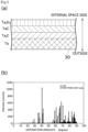
- the tantalum silicide layer having a composition of TaSi 2 is formed as shown in Fig. 2(a).
- Fig. 2 (b) shows a X-ray diffraction pattern of the tantalum silicide layer that is formed as above. Peaks marked with circles in Fig. 2 (b) show tantalum carbide, and the other peaks show TaSi 2 .
- TaSi 2 is sufficiently formed by forming the tantalum silicide layer using the above-described method.
- Ta 5 Si 3 other than TaSi 2 can be also formed as the tantalum silicide layer (see Fig. 3(a) ).
- Si that is vaporized in the same manner as above is introduced in the internal space of the crucible, and heated for 15 minutes at 2000°C under reduced pressure 10Pa or less.
- Fig. 3(b) shows a X-ray diffraction pattern of the tantalum silicide layer that is formed as above. Peaks marked with circles in Fig. 3 (b) show tantalum carbide, and the other peaks show Ta 5 Si 3 . As such, it can be seen that Ta 5 Si 3 is sufficiently formed by forming the tantalum silicide layer using the above-described method.
- Fig. 4 shows a graph showing a partial pressure of Si vapor pressure of Si, SiC, TaSi 2 , and Ta 5 Si 3 . It can be seen that Si vapor pressure that is supplied from TaSi 2 and Ta 5 Si 3 indicates a considerable high pressure. Therefore, it is clear that the tantalum silicide layer is a supply source of Si for the internal space of the crucible 30. The tantalum silicide layer is provided over an entire wall surface that defines the internal space. This allows the pressure distribution of Si pressure in the internal space to be uniform. Therefore, the SiC substrate 40 can be etched uniformly.
- Si vapor pressure etching that is performed in this embodiment (hereinafter, simply referred to as the etching) will be described, and difference in the rate of etching when using the crucible 30 having a different composition will be also described with reference to Fig. 5 and Fig. 6 .
- the SiC substrate 40 stored in the crucible 30 is heated under high-purity Si vapor pressure up to a temperature of 1500°C or more and 2200°C or less and desirably 1600°C or more and 2000°C or less by using the high temperature vacuum furnace 10.
- This can etch the surface of the SiC substrate 40.
- the following reactions are performed. Briefly, the SiC substrate 40 is heated under Si vapor pressure, and thereby Si vapor is eliminated from SiC by thermal decomposition. Si vapor is supplied from the tantalum silicide layer. C that is remained by Si vapor eliminated by thermal decomposition reacts with Si vapor, and thereby sublimates into Si 2 C or SiC 2 .
- the rate of etching is closely relevant to the rate at which SiC 2 and Si 2 C absorb C atoms. Therefore, it is considered that the rate of etching is higher in accordance with the higher ratio of the amount of tantalum substance that is contained in the compound for forming the tantalum silicide layer.
- the pressure equilibrium constant of the reaction between SiC 2 and TaSi 2 is smaller than the pressure equilibrium constant of the reaction between SiC 2 and Ta 5 Si 3 .
- the rate of etching when using the crucible 30 having the tantalum silicide layer of TaSi 2 is slower than the rate of etching when using the crucible 30 having the tantalum silicide layer of Ta 5 Si 3 .
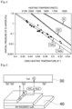
- Fig. 6 is a diagram showing a result when a 4H-SiC (0001) face having an off angle of 4° is etched in a temperature range from 1650°C to 2100°C under high vacuum (10 -4 Pa) in using the crucible 30 having the tantalum silicide layer of TaSi 2 and using the crucible 30 having the tantalum silicide layer of Ta 5 Si 3 .
- a graph of Fig. 6 it is confirmed that the crucible 30 containing TaSi 2 has a considerably slower rate etching than that of the crucible 30 containing Ta 5 Si 3 .
- the crucibles 30 having a different composition of the tantalum silicide layer are used, which can easily change the rate of etching without changing the heating temperature and the like.
- a specific situation for using the crucibles 30 will be described.
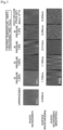
- Fig. 7 is a diagram showing a photomicrograph and a surface roughness of a surface of the SiC substrate 40 when the etching is performed with the change of an inert gas (Ar gas) pressure in etching (that is, the rate of etching). As shown in Fig.
- the etching (high rate etching) is merely performed by using the crucible 30 having the tantalum silicide layer of Ta 5 Si 3 when manufacturing the SiC substrate 40 in which the step bunching is not generated.
- the etching (low rate etching) is merely performed by using the crucible 30 having the tantalum silicide layer of TaSi 2 when manufacturing the SiC substrate 40 in which the step bunching is generated.
- a modified layer having disordered crystallinity that is formed by applying the pressure on the surface of the SiC substrate 40 during mechanical polishing and the like may have several tens of ⁇ m of the depth in some cases.
- a high rate polishing of the SiC substrate 40 is also needed. Therefore, the etching (high rate etching) can be performed easier than the conventional etching by using the crucible 30 having the tantalum silicide layer of Ta 5 Si 3 , instead of mechanical polishing and chemical mechanical polishing, etc. or in order to remove the latent scratches.
- an activation annealing step of the SiC substrate 40 having an epitaxial growth layer in which ions are implanted an epitaxial layer growth, an ion implantation, and an activation of impurities implanted as ions (hereinafter, referred to as dopant) are performed with respect to the SiC substrate 40.
- the etching is performed for removing a dopant insufficient region and planarizing the surface that is roughened by ion implantation.
- the dopant insufficient region exists in a region from the surface of the SiC substrate 40 to a depth about several tens to hundreds of nm, for example, depending on the ion implantation conditions. Fig.
- FIG. 8 shows one example of the dopant concentration in accordance with the depth from the surface of the SiC substrate 40.
- Fig. 8 there is low dopant concentration in a region from the surface to a depth of several tens of nm, and the dopant concentration decreases as the depth is deeper than about 500nm. Therefore, since the amount of etching needs to be precisely controlled in order to remain a region having a sufficient dopant concentration while removing the dopant insufficient region, it is preferable to set a low rate etching. However, as described above, when the rate of etching is lower than the predetermined rate of etching, the step bunching cannot be removed.
- a precise etching (low rate etching) is merely performed by using the crucible 30 having the tantalum silicide layer of TaSi 2 under a condition that the step bunching is not generated.
- the crucibles 30 having a different composition of the tantalum silicide layer are used in removing the latent scratches and in etching after ion implantation, which can perform the etching at an appropriate rate of etching without significantly changing the heating temperature and the like.
- the SiC substrate 40 stored in the crucible 30 is etched by heating under Si vapor pressure.
- the crucible 30 is formed of a tantalum metal, and has a tantalum carbide layer provided on an internal space side of the tantalum metal, and a tantalum silicide layer provided on the side further toward the internal space side than the tantalum carbide layer. Then, the rate of etching of the SiC substrate 40 is controlled based on difference in a composition of the tantalum silicide layer.
- the rate of etching of the SiC substrate 40 can be controlled without changing the heating temperature and the Si pressure.
- At least two crucibles 30 in which their compositions of the tantalum silicide layer are different from each other are used depending on performed processes.
- high rate etching and low rate etching can be performed.
- the crucible 30 having a higher ratio of tantalum occupied in one molecule of the compound for forming the tantalum silicide layer (to be specific, Ta 5 Si 3 ) is used.
- the crucible 30 having a lower ratio of tantalum occupied in one molecule of the compound for forming the tantalum silicide layer (to be specific, TaSi 2 ) is used.
- TaSi 2 and Ta 5 Si 3 are formed as a tantalum silicide
- the tantalum silicide represented by other chemical formula may be also adoptable.
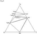
- Ta 2 Si, Ta 3 Si or Ta 5 Si 3 C 0.5 may be formed.
- it may be considered as the tantalum silicide layer even if other atoms are included like Ta 5 Si 3 C 0.5 .
- the tantalum silicide having a same composition is formed over the entire inner wall of one crucible 30
- the tantalum silicide having a plurality of kinds of compositions may be formed on the inner wall of one crucible 30.
- the rate of etching on only a part of the surface of the SiC substrate 40 can be high or low. In consideration of such rate of etching, the SiC substrate 40 having a desired shape can be created.
- a heating apparatus other than the above-described high temperature vacuum furnace 10 may be used, or a container having shapes or materials different from the crucible 30 may be used.
- an external shape of the storing container is not limited to a cylindrical shape, and may have a cubic shape or a rectangular parallelepiped shape.
Landscapes
- Chemical & Material Sciences (AREA)
- Engineering & Computer Science (AREA)
- Organic Chemistry (AREA)
- Crystallography & Structural Chemistry (AREA)
- Materials Engineering (AREA)
- Metallurgy (AREA)
- Inorganic Chemistry (AREA)
- Physics & Mathematics (AREA)
- Plasma & Fusion (AREA)
- Crystals, And After-Treatments Of Crystals (AREA)
- Chemical Kinetics & Catalysis (AREA)
- General Chemical & Material Sciences (AREA)
- Drying Of Semiconductors (AREA)
Description
- The present invention relates mainly to a method for etching a SiC substrate by using a storing container having a tantalum silicide layer that is provided on an internal space side.
- Conventionally, a method for etching a surface of a SiC substrate by heating the SiC substrate that is stored in a storing container under a state where a high-purity Si vapor pressure is caused within the storing container has been conventionally known (Si vapor pressure etching).
Patent Documents -
Patent Document 1 discloses a method for placing Si pellets (solid Si) in the storing container in order to cause Si vapor pressure within the storing container.Patent Document 2 discloses a method for adhering Si on an inner wall surface in the storing container in order to cause Si vapor pressure within the storing container. - Here, in the method of
Patent Document 1, Si pressure distribution may be ununiform. In the method ofPatent Document 2, Si that is adhered to an upper wall surface of the storing container, for example, may be melted and dropped onto the SiC substrate. - In view of the circumstances described above, Patent Document 3 proposes a method in which a storing container has a tantalum silicide layer that is provided on an internal space side of the storing container, and the tantalum silicide layer is a supply source of Si vapor.
Patent Document 4 provides a storing container wherein Si does not drop onto a single crystal SiC substrate, and Si pressure distribution in an internal space can be made uniform. -
- PATENT DOCUMENT 1:
Japanese Patent Application Laid-Open No. 2011-233780 - PATENT DOCUMENT 2:
Japanese Patent Application Laid-Open No. 2008-230944 - PATENT DOCUMENT 3:
Japanese Patent Application Laid-Open No. 2014-103180 - PATENT DOCUMENT 4:
WO 2014/076964 A1 - Recently, control of an rate of etching is regarded as important. For example, although a step bunching may be generated by heating a SiC substrate, it has been known whether the step bunching can be removed or not depends on the rate of etching. Here, when a Si vapor pressure etching is applied to a SiC manufacturing process, a technical problem with regard to the rate of etching of the SiC substrate in a treatment step of the SiC substrate for an epitaxial growth and in an activation annealing step of the SiC substrate having an epitaxial growth layer in which ions are implanted will be described.
- Firstly, the treatment step of the SiC substrate for the epitaxial growth will be described. The SiC substrate can be obtained by cutting out of an ingot in a predetermined thickness. Since a surface roughness in a state of the SiC substrate that is cut out of the ingot is large, the surface needs to be planarized by performing the treatment steps such as mechanical polishing (MP) and chemical mechanical polishing (CMP). Although polishing scratches that remains on the surface of the SiC substrate are substantially removed by mechanical polishing and chemical mechanical polishing, a part of deep polishing scratches or a modified layer having disordered crystallinity that is formed by applying the pressure on the surface of the SiC substrate during mechanical polishing and chemical mechanical polishing (hereinafter, referred to as latent scratches) may remain. Since such polishing scratches or latent scratches may have several tens of µm of the depth in some cases, the higher rate etching is desired for efficiently removing the scratches.
- In the activation step of the SiC substrate having the epitaxial growth layer in which ions are implanted, a sufficient temperature for replacing (activating) impurities (hereinafter, referred to as dopant) that are implanted as ions with a SiC crystal lattice location needs to be provided, and a dopant insufficient region having an insufficient dopant concentration that exists on the surface of the SiC substrate to a predetermined depth (about several tens to hundreds of nm-order) needs to be precisely removed by the etching. However, if the SiC substrate is excessively etched, a region having the sufficient dopant concentration is removed. Therefore, with respect to the SiC substrate having the epitaxial growth layer in which the ions are implanted, since the depth of etching needs to be accurately controlled with the rate of etching in which the step bunching is not generated, it is preferable to appropriately reduce the rate of etching.
- The heating temperature, Si pressure, and inert gas pressure has been known as parameters relating to the rate of etching. However, since it may be considered that control of these parameters affects conditions other than the rate of etching, it is preferable that the rate of etching can be controlled by various methods.
- The present invention has been made in view of the circumstances described above, a primary object is to provide an etching method for controlling the rate of etching of a SiC substrate based on a composition of a storing container.
- Problems to be solved by the present invention are as described above, and next, means for solving the problems and effects thereof will be described.
- In a first aspect of the present invention, the etching method of a SiC substrate according to
claim 1 is provided. - Accordingly, the rate of etching can be controlled without changing a heating temperature, a Si pressure, and the like.
- In the etching method of the SiC substrate, the tantalum silicide layer preferably includes any one of TaSi2, Ta5Si3, Ta2Si, Ta3Si, Ta5Si3C0.5.
- Accordingly, the rate of etching can be controlled by using a general compound that is composed of Ta and Si.
- In the etching method of the SiC substrate, two storing containers in which their compositions of the tantalum silicide layer are different from each other are used depending on the performed processes.
- Accordingly, merely with the change of the storing containers, the process having a different required rate of etching can be performed without changing the temperature conditions and the like.
- The etching method of the SiC substrate is configured as follows. That is, high rate etching and low rate etching can be performed. In the high rate etching, the storing container having a higher ratio of tantalum occupied in one molecule of the compound for forming the tantalum silicide layer is used. In the low rate etching, the storing container having a lower ratio of tantalum occupied in one molecule of the compound for forming the tantalum silicide layer is used.
- Accordingly, since carbon atoms in atmosphere are likely to be absorbed in a higher ratio of tantalum, the rate of etching is high. Therefore, as described above, either one of the storing containers is used, which can perform the etching at an appropriate rate.
- In a second aspect of the present invention, the use of a storing container in the etching method of the SiC substrate is provided.
- Accordingly, the storing container in which the rate of etching of the SiC substrate can be controlled without changing the heating temperature and the Si pressure and the like.
-
- [
Fig. 1 ] A diagram for illustration of an outline of a high temperature vacuum furnace for use in an etching method according to the present invention. - [
Fig. 2 ] A drawing showing a configuration of a wall surface of a crucible for a low rate etching and a X-ray diffraction pattern of the crucible. - [
Fig. 3 ] A drawing showing a configuration of a wall surface of a crucible for a high rate etching and a X-ray diffraction pattern of the crucible. - [
Fig. 4 ] A graph showing a change of a partial pressure depending on a temperature of Si and Si compound. - [
Fig. 5 ] A schematic diagram for illustration of a carbon adsorption function of the crucible. - [
Fig. 6 ] A graph comparing the rate of etching when using a crucible having an inner wall surface of TaSi2 with the rate of etching when using a crucible having an inner wall surface of Ta3Si5. - [
Fig. 7 ] A diagram showing a photomicrograph and a surface roughness of a surface of a SiC substrate when the etching is performed with the change of an inert gas pressure in etching (that is, the rate of etching). - [
Fig. 8 ] A graph showing a dopant concentration, particularly a dopant insufficient region, depending on a depth from the surface of the SiC substrate. - [
Fig. 9 ] A phase diagram of Ta-C-Si. - Next, an embodiment of the present invention will be described with reference to the drawings. Firstly, referring to
Fig. 1 , a hightemperature vacuum furnace 10 used for a heat treatment of this embodiment will be described. - As shown in
Fig. 1 , the hightemperature vacuum furnace 10 includes amain heating chamber 21 and apreheating chamber 22. Themain heating chamber 21 is configured to heat a SiC substrate 40 (single crystal SiC substrate) made of, at least in its surface, single crystal SiC, up to a temperature of 1000°C or more and 2300°C or less. Thepreheating chamber 22 is a space for preheating a SiC substrate prior to heating of theSiC substrate 40 in themain heating chamber 21. - A vacuum-forming
valve 23, an inertgas injection valve 24, and avacuum gauge 25 are connected to themain heating chamber 21. The vacuum-formingvalve 23 is configured to adjust the degree of vacuum of themain heating chamber 21. The inertgas injection valve 24 is configured to adjust the pressure of an inert gas (for example, Ar gas) contained in themain heating chamber 21. Thevacuum gauge 25 is configured to measure the degree of vacuum of the interior of themain heating chamber 21. -
Heaters 26 are provided in themain heating chamber 21. A heat reflection metal plate (not shown) is secured to a side wall and a ceiling of themain heating chamber 21. The heat reflection metal plate is configured to reflect heat of theheaters 26 toward a central region of themain heating chamber 21. This provides strong and uniform heating of theSiC substrate 40, to cause a temperature rise up to 1000°C or more and 2300°C or less. Examples of theheaters 26 include resistive heaters and high-frequency induction heaters. - The
SiC substrate 40 is heated while stored in a crucible (storing container) 30. Thecrucible 30 is placed on an appropriate support or the like, and the support is movable at least in a range from the preheating chamber to the main heating chamber. Thecrucible 30 includes anupper container 31 and alower container 32 that are fittable with each other. Detailed configuration of thecrucible 30 will be described later. - To perform a heat treatment of the
SiC substrate 40, thecrucible 30 is firstly placed in the preheatingchamber 22 of the hightemperature vacuum furnace 10 as indicated by the dot-dash lines inFig. 1 , and preheated at an appropriate temperature (for example, about 800°C). Then, thecrucible 30 is moved to themain heating chamber 21 whose temperature has been elevated to a set temperature (for example, about 1800°C) in advance. After that, theSiC substrate 40 is heated while adjusting the pressure and the like. The preheating may be omitted. - Next, a composition of a wall surface of the
crucible 30 and a method for forming a tantalum silicide layer will be described with reference toFig. 2 andFig. 3 . - The
crucible 30 has a configuration shown inFig. 2 , in its portion constituting wall surfaces (an upper surface, a side surface, and a bottom surface) that define an internal space in which theSiC substrate 40 is stored. More specifically, a tantalum layer (Ta), a tantalum carbide layer (TaC and Ta2C), and a tantalum silicide layer (TaSi2, Ta5Si3 or the like) are provided in this order from the outside toward the internal space side. - The tantalum silicide layer supplies Si to the internal space. Since the
crucible 30 includes the tantalum layer and the tantalum carbide layer, surrounding C vapor can be absorbed. Accordingly, a high-purity Si atmosphere can be caused in the internal space. - The crucible made of the tantalum layer and the tantalum carbide layer has been conventionally known. In this embodiment, the tantalum silicide layer is formed in the crucible. More specifically, Si that is vaporized at high temperature in advance is arranged in the internal space of the crucible, and heated for 15 minutes at 1800°C under reduced pressure 10Pa or less. Thereby, the tantalum silicide layer having a composition of TaSi2 is formed as shown in
Fig. 2(a). Fig. 2 (b) shows a X-ray diffraction pattern of the tantalum silicide layer that is formed as above. Peaks marked with circles inFig. 2 (b) show tantalum carbide, and the other peaks show TaSi2. As such, it can be seen that TaSi2 is sufficiently formed by forming the tantalum silicide layer using the above-described method. - Ta5Si3 other than TaSi2 can be also formed as the tantalum silicide layer (see
Fig. 3(a) ). In this case, Si that is vaporized in the same manner as above is introduced in the internal space of the crucible, and heated for 15 minutes at 2000°C under reduced pressure 10Pa or less.Fig. 3(b) shows a X-ray diffraction pattern of the tantalum silicide layer that is formed as above. Peaks marked with circles inFig. 3 (b) show tantalum carbide, and the other peaks show Ta5Si3. As such, it can be seen that Ta5Si3 is sufficiently formed by forming the tantalum silicide layer using the above-described method. -
Fig. 4 shows a graph showing a partial pressure of Si vapor pressure of Si, SiC, TaSi2, and Ta5Si3. It can be seen that Si vapor pressure that is supplied from TaSi2 and Ta5Si3 indicates a considerable high pressure. Therefore, it is clear that the tantalum silicide layer is a supply source of Si for the internal space of thecrucible 30. The tantalum silicide layer is provided over an entire wall surface that defines the internal space. This allows the pressure distribution of Si pressure in the internal space to be uniform. Therefore, theSiC substrate 40 can be etched uniformly. - Next, Si vapor pressure etching that is performed in this embodiment (hereinafter, simply referred to as the etching) will be described, and difference in the rate of etching when using the
crucible 30 having a different composition will be also described with reference toFig. 5 andFig. 6 . - In this embodiment, the
SiC substrate 40 stored in thecrucible 30 is heated under high-purity Si vapor pressure up to a temperature of 1500°C or more and 2200°C or less and desirably 1600°C or more and 2000°C or less by using the hightemperature vacuum furnace 10. This can etch the surface of theSiC substrate 40. In the etching, the following reactions are performed. Briefly, theSiC substrate 40 is heated under Si vapor pressure, and thereby Si vapor is eliminated from SiC by thermal decomposition. Si vapor is supplied from the tantalum silicide layer. C that is remained by Si vapor eliminated by thermal decomposition reacts with Si vapor, and thereby sublimates into Si2C or SiC2.
(1) SiC(s) → Si(v)I + C(s)
(2) Tax Siy → Si(v)II + Tax' ,Siy'
(3) 2C(s) + Si(v)I + II SiC2 (v)
(4) C(s) + 2Si(v)I + II→ Si2C(v)
- When the above reactions continue, SiC2 and Si2C that are generated in the chemical formulas (3) and (4) are excessive, which results in a decrease in the reaction rate of the chemical formulas (1) to (4). However, in this embodiment, when the
crucible 30 shown inFig. 2 is used, TaC and Si are generated by reacting between SiC2 and TaSi2. When thecrucible 30 shown inFig. 3 is used, Ta2C and TaSi2 are generated by the reaction between SiC2 and Ta5Si3. As such, C included in SiC2 is absorbed in tantalum of the crucible 30 (seeFig. 5 ). When Si is generated, Si is used for the reaction for removing C atoms that remain in theSiC substrate 40 again. As described above, the etching continues to perform without reducing the reaction rate. - In consideration of the above, it can be seen that the rate of etching is closely relevant to the rate at which SiC2 and Si2C absorb C atoms. Therefore, it is considered that the rate of etching is higher in accordance with the higher ratio of the amount of tantalum substance that is contained in the compound for forming the tantalum silicide layer. The pressure equilibrium constant of the reaction between SiC2 and TaSi2 is smaller than the pressure equilibrium constant of the reaction between SiC2 and Ta5Si3. As above, it is considered that the rate of etching when using the
crucible 30 having the tantalum silicide layer of TaSi2 is slower than the rate of etching when using thecrucible 30 having the tantalum silicide layer of Ta5Si3. -
Fig. 6 is a diagram showing a result when a 4H-SiC (0001) face having an off angle of 4° is etched in a temperature range from 1650°C to 2100°C under high vacuum (10-4 Pa) in using thecrucible 30 having the tantalum silicide layer of TaSi2 and using thecrucible 30 having the tantalum silicide layer of Ta5Si3. In a graph ofFig. 6 , it is confirmed that thecrucible 30 containing TaSi2 has a considerably slower rate etching than that of thecrucible 30 containing Ta5Si3. - As such, in this embodiment, the
crucibles 30 having a different composition of the tantalum silicide layer are used, which can easily change the rate of etching without changing the heating temperature and the like. In the following, a specific situation for using thecrucibles 30 will be described. - According to the experiment by the applicants, it was confirmed that a step bunching was removed by setting the rate of etching over a predetermined threshold, and in the rate of etching smaller than the predetermined threshold, the step bunching could not be removed even when the etching was performed for a long time.
Fig. 7 is a diagram showing a photomicrograph and a surface roughness of a surface of theSiC substrate 40 when the etching is performed with the change of an inert gas (Ar gas) pressure in etching (that is, the rate of etching). As shown inFig. 7 , under a condition of the experiment, when the inert gas pressure is 1.3 kPa, it can be seen by the photomicrograph that the surface roughness is large and the step bunching is clearly remaining. When the inert gas pressure is 133 Pa, it can be seen by the photomicrograph that the surface roughness is markedly reduced and the step bunching is partly removed. When the inert gas pressure is 13 Pa and 1.3 Pa under high vacuum, it can be seen by the photomicrograph that the surface roughness is further reduced and substantially entire step bunching is also removed. As such, whether or not the step bunching is removed can be selected in accordance with the inert gas pressure (that is, the rate of etching). In theSiC substrate 40 in which the step bunching is not generated, local concentration or the like of the electric field does not occur. This leads to high performance as a semiconductor element. However, in theSiC substrate 40 in which the step bunching is generated, it is known that an effect of crystal defect (dislocation) can be further eliminated when the solution growth method is performed, for example. Therefore, it is preferable to switch the presence and absence of generation of the step bunching, depending the situations. - In this embodiment, since the rate of etching can be switched merely by using the
crucible 30, the etching (high rate etching) is merely performed by using thecrucible 30 having the tantalum silicide layer of Ta5Si3 when manufacturing theSiC substrate 40 in which the step bunching is not generated. On the other hand, the etching (low rate etching) is merely performed by using thecrucible 30 having the tantalum silicide layer of TaSi2 when manufacturing theSiC substrate 40 in which the step bunching is generated. - Next, another situation for using the
crucibles 30 will be described. Firstly, in a treatment step of theSiC substrate 40 for an epitaxial growth, an ingot including 4H-SiC single crystal or 6H-SiC single crystal is cut out in a predetermined thickness. Thereafter, treatments such as mechanical polishing and chemical mechanical polishing, etc. are performed for removing a surface roughness that is formed on the surface of theSiC substrate 40 in cutting. Since the surface roughness has considerably large difference in height, a high rate polishing of theSiC substrate 40 is needed. In addition, a modified layer having disordered crystallinity that is formed by applying the pressure on the surface of theSiC substrate 40 during mechanical polishing and the like (hereinafter, referred to as latent scratches) may have several tens of µm of the depth in some cases. In removing such latent scratches, a high rate polishing of theSiC substrate 40 is also needed. Therefore, the etching (high rate etching) can be performed easier than the conventional etching by using thecrucible 30 having the tantalum silicide layer of Ta5Si3, instead of mechanical polishing and chemical mechanical polishing, etc. or in order to remove the latent scratches. - In an activation annealing step of the
SiC substrate 40 having an epitaxial growth layer in which ions are implanted, an epitaxial layer growth, an ion implantation, and an activation of impurities implanted as ions (hereinafter, referred to as dopant) are performed with respect to theSiC substrate 40. Then, the etching is performed for removing a dopant insufficient region and planarizing the surface that is roughened by ion implantation. Specifically, the dopant insufficient region exists in a region from the surface of theSiC substrate 40 to a depth about several tens to hundreds of nm, for example, depending on the ion implantation conditions.Fig. 8 shows one example of the dopant concentration in accordance with the depth from the surface of theSiC substrate 40. InFig. 8 , there is low dopant concentration in a region from the surface to a depth of several tens of nm, and the dopant concentration decreases as the depth is deeper than about 500nm. Therefore, since the amount of etching needs to be precisely controlled in order to remain a region having a sufficient dopant concentration while removing the dopant insufficient region, it is preferable to set a low rate etching. However, as described above, when the rate of etching is lower than the predetermined rate of etching, the step bunching cannot be removed. Therefore, in order to prevent a region having a sufficient dopant concentration from excessively removing, a precise etching (low rate etching) is merely performed by using thecrucible 30 having the tantalum silicide layer of TaSi2 under a condition that the step bunching is not generated. - Accordingly, the
crucibles 30 having a different composition of the tantalum silicide layer are used in removing the latent scratches and in etching after ion implantation, which can perform the etching at an appropriate rate of etching without significantly changing the heating temperature and the like. - As described above, in the etching method of this embodiment, the
SiC substrate 40 stored in thecrucible 30 is etched by heating under Si vapor pressure. Thecrucible 30 is formed of a tantalum metal, and has a tantalum carbide layer provided on an internal space side of the tantalum metal, and a tantalum silicide layer provided on the side further toward the internal space side than the tantalum carbide layer. Then, the rate of etching of theSiC substrate 40 is controlled based on difference in a composition of the tantalum silicide layer. - Accordingly, the rate of etching of the
SiC substrate 40 can be controlled without changing the heating temperature and the Si pressure. - In the etching method of the
SiC substrate 40 of this embodiment, at least twocrucibles 30 in which their compositions of the tantalum silicide layer are different from each other (to be specific, TaSi2 and Ta5Si3) are used depending on performed processes. - Accordingly, merely with the change of the
crucible 30, the processes having a different required rate of etching can be performed without changing the temperature conditions or the like. - In the etching method of the
SiC substrate 40 of this embodiment, high rate etching and low rate etching can be performed. In the high rate etching, thecrucible 30 having a higher ratio of tantalum occupied in one molecule of the compound for forming the tantalum silicide layer (to be specific, Ta5Si3) is used. In the low rate etching, thecrucible 30 having a lower ratio of tantalum occupied in one molecule of the compound for forming the tantalum silicide layer (to be specific, TaSi2) is used. - Accordingly, since carbon atoms in atmosphere are likely to be absorbed in a case of a higher ratio of tantalum, the rate of etching is high. Therefore, as described above, either one of the
crucibles 30 is used, which can perform the etching at an appropriate rate. - Although a preferred embodiment of the present invention has been described above, the above-described configuration can be modified, for example, as follows.
- In the above-described embodiment, although TaSi2 and Ta5Si3 are formed as a tantalum silicide, the tantalum silicide represented by other chemical formula may be also adoptable. For example, as shown in a phase diagram of
Fig. 9 , Ta2Si, Ta3Si or Ta5Si3C0.5 may be formed. In the specification, it may be considered as the tantalum silicide layer even if other atoms are included like Ta5Si3C0.5. - In the above-described embodiment, although a tantalum silicide having a same composition is formed over the entire inner wall of one
crucible 30, the tantalum silicide having a plurality of kinds of compositions may be formed on the inner wall of onecrucible 30. In this case, the rate of etching on only a part of the surface of theSiC substrate 40 can be high or low. In consideration of such rate of etching, theSiC substrate 40 having a desired shape can be created. - The above-described temperature conditions, pressure conditions and the like are merely illustrative ones, and can be modified as appropriate. A heating apparatus other than the above-described high
temperature vacuum furnace 10 may be used, or a container having shapes or materials different from thecrucible 30 may be used. For example, an external shape of the storing container is not limited to a cylindrical shape, and may have a cubic shape or a rectangular parallelepiped shape. -
- 10
- high temperature vacuum furnace
- 30
- crucible (storing container)
- 40
- SiC substrate
Claims (4)
- An etching method for etching a SiC substrate that is stored in a storing container, by heating the SiC substrate under Si vapor pressure, whereinthe storing container is formed of a tantalum metal, and a tantalum carbide layer is provided on an internal space side of the tantalum metal, and a tantalum silicide layer is provided on the side further toward the internal space side than the tantalum carbide layer,the rate of etching of the SiC substrate is controlled in accordance with the ratio of the amount of tantalum substance that is contained in the compound for forming the tantalum silicide layer,at least two storing containers in which compositions of the tantalum silicide layer are different from each other are used depending on performed processes, anda high rate etching and low rate etching can be performed,in the high rate etching, the storing container having a higher ratio of tantalum occupied in one molecule of a compound for forming the tantalum silicide layer is used,in the low rate etching, the storing container having a lower ratio of tantalum occupied in one molecule of the compound for forming the tantalum silicide layer is used.
- The etching method of the SiC substrate according to claim 1, wherein
the tantalum silicide layer includes any one of TaSi2, Ta5Si3, Ta2Si, Ta3Si, and Ta5Si3C0.5. - Use of the storing container defined in claim 1 in the etching method according to claim 1.
- Use according to claim 3, wherein the tantalum silicide layer of the container includes any one of TaSi2, Ta5Si3, Ta2Si, and Ta5Si3C0.5.
Applications Claiming Priority (2)
| Application Number | Priority Date | Filing Date | Title |
|---|---|---|---|
| JP2014233631 | 2014-11-18 | ||
| PCT/JP2015/005742 WO2016079983A1 (en) | 2014-11-18 | 2015-11-17 | Etching method for sic substrate and holding container |
Publications (3)
| Publication Number | Publication Date |
|---|---|
| EP3223303A1 EP3223303A1 (en) | 2017-09-27 |
| EP3223303A4 EP3223303A4 (en) | 2018-05-30 |
| EP3223303B1 true EP3223303B1 (en) | 2023-03-15 |
Family
ID=56013556
Family Applications (1)
| Application Number | Title | Priority Date | Filing Date |
|---|---|---|---|
| EP15861337.2A Active EP3223303B1 (en) | 2014-11-18 | 2015-11-17 | Etching method for sic substrate and use of holding container |
Country Status (7)
| Country | Link |
|---|---|
| US (1) | US10388536B2 (en) |
| EP (1) | EP3223303B1 (en) |
| JP (1) | JP6751874B2 (en) |
| KR (1) | KR20170085085A (en) |
| CN (1) | CN107004592B (en) |
| TW (1) | TWI659463B (en) |
| WO (1) | WO2016079983A1 (en) |
Families Citing this family (13)
| Publication number | Priority date | Publication date | Assignee | Title |
|---|---|---|---|---|
| JP2018199591A (en) * | 2017-05-25 | 2018-12-20 | 東洋炭素株式会社 | METHOD FOR MANUFACTURING SiC WAFER, METHOD FOR MANUFACTURING EPITAXIAL WAFER AND EPITAXIAL WAFER |
| EP3936643A4 (en) * | 2019-03-05 | 2022-11-09 | Kwansei Gakuin Educational Foundation | METHOD AND APPARATUS FOR PRODUCING A SIC SUBSTRATE |
| EP3936645A4 (en) * | 2019-03-05 | 2022-11-09 | Kwansei Gakuin Educational Foundation | METHOD AND DEVICE FOR MANUFACTURING A SIC SUBSTRATE AND METHOD FOR REDUCING THE CONCENTRATION OF MACRO-EXTRA THICKNESSES OF THE SIC SUBSTRATE |
| JP7464808B2 (en) * | 2019-03-05 | 2024-04-10 | 学校法人関西学院 | Method and apparatus for manufacturing SiC substrate, and method for reducing process-affected layer of SiC substrate |
| WO2020203516A1 (en) | 2019-03-29 | 2020-10-08 | 学校法人関西学院 | Device for manufacturing semiconductor substrate comprising temperature gradient inversion means and method for manufacturing semiconductor substrate |
| EP4012077A4 (en) | 2019-08-06 | 2023-09-20 | Kwansei Gakuin Educational Foundation | METHOD FOR PRODUCING SIC SUBSTRATE |
| WO2021025084A1 (en) | 2019-08-06 | 2021-02-11 | 学校法人関西学院 | SiC SEED CRYSTAL AND METHOD FOR PRODUCING SAME, SiC INGOT PRODUCED BY GROWING SAID SiC SEED CRYSTAL AND METHOD FOR PRODUCING SAME, AND SiC WAFER PRODUCED FROM SAID SiC INGOT AND SiC WAFER WITH EPITAXIAL FILM AND METHODS RESPECTIVELY FOR PRODUCING SAID SiC WAFER AND SAID SiC WAFER WITH EPITAXIAL FILM |
| US12421624B2 (en) | 2019-08-06 | 2025-09-23 | Kwansei Gakuin Educational Foundation | SiC substrate, SiC epitaxial substrate, SiC ingot and production methods thereof |
| JP7274154B2 (en) * | 2019-08-06 | 2023-05-16 | 株式会社デンソー | SiC substrate manufacturing method |
| CN113550012B (en) * | 2021-07-28 | 2022-11-18 | 浙江大学杭州国际科创中心 | Device for etching silicon carbide wafer by alkali steam |
| WO2023189056A1 (en) * | 2022-03-31 | 2023-10-05 | ローム株式会社 | Furnace core tube, heat treatment apparatus and support unit |
| CN121752767A (en) * | 2023-09-15 | 2026-03-27 | 学校法人关西学院 | Method for treating SiC substrate, method for removing processed modified layer of SiC substrate, and method for reducing surface roughness of SiC substrate |
| CN117080061A (en) * | 2023-10-16 | 2023-11-17 | 希科半导体科技(苏州)有限公司 | Planarization method of silicon carbide substrate, silicon carbide substrate and semiconductor device |
Family Cites Families (14)
| Publication number | Priority date | Publication date | Assignee | Title |
|---|---|---|---|---|
| US6547877B2 (en) * | 1996-01-22 | 2003-04-15 | The Fox Group, Inc. | Tantalum crucible fabrication and treatment |
| JP5213095B2 (en) | 2007-03-23 | 2013-06-19 | 学校法人関西学院 | Method for planarizing surface of single crystal silicon carbide substrate, method for manufacturing single crystal silicon carbide substrate, and single crystal silicon carbide substrate |
| JP5464544B2 (en) * | 2009-05-12 | 2014-04-09 | 学校法人関西学院 | Single crystal SiC substrate with epitaxial growth layer, carbon supply feed substrate, and SiC substrate with carbon nanomaterial |
| JP5564682B2 (en) * | 2010-04-28 | 2014-07-30 | 学校法人関西学院 | Manufacturing method of semiconductor device |
| JP6093154B2 (en) * | 2012-11-16 | 2017-03-08 | 東洋炭素株式会社 | Method for manufacturing container |
| TWI600081B (en) * | 2012-11-16 | 2017-09-21 | 東洋炭素股份有限公司 | Surface treatment method of single crystal silicon carbide substrate and single crystal silicon carbide substrate |
| US20140342553A1 (en) * | 2013-05-14 | 2014-11-20 | United Microelectronics Corp. | Method for Forming Semiconductor Structure Having Opening |
| JP6080075B2 (en) * | 2013-06-13 | 2017-02-15 | 学校法人関西学院 | Surface treatment method for SiC substrate |
| WO2015009495A1 (en) * | 2013-07-17 | 2015-01-22 | Cook Medical Technologies Llc | Ablation mesh |
| JP6247566B2 (en) * | 2014-02-28 | 2017-12-13 | 東洋炭素株式会社 | Heat treatment container, heat treatment container assembly, and semiconductor device manufacturing apparatus |
| JP6232329B2 (en) * | 2014-03-31 | 2017-11-15 | 東洋炭素株式会社 | Method for removing work-affected layer of SiC seed crystal, method for producing SiC seed crystal and SiC substrate |
| JP6330531B2 (en) * | 2014-07-08 | 2018-05-30 | 株式会社リコー | Image recording system and image recording method |
| KR102549160B1 (en) * | 2014-11-18 | 2023-06-30 | 토요타 쯔우쇼우 가부시키가이샤 | Sic substrate treatment method |
| KR20170086068A (en) * | 2014-11-18 | 2017-07-25 | 토요 탄소 가부시키가이샤 | Surface treatment method for sic substrate |
-
2015
- 2015-11-17 WO PCT/JP2015/005742 patent/WO2016079983A1/en not_active Ceased
- 2015-11-17 KR KR1020177016190A patent/KR20170085085A/en not_active Abandoned
- 2015-11-17 EP EP15861337.2A patent/EP3223303B1/en active Active
- 2015-11-17 JP JP2016560059A patent/JP6751874B2/en active Active
- 2015-11-17 CN CN201580062705.9A patent/CN107004592B/en active Active
- 2015-11-17 US US15/527,622 patent/US10388536B2/en active Active
- 2015-11-18 TW TW104138126A patent/TWI659463B/en not_active IP Right Cessation
Also Published As
| Publication number | Publication date |
|---|---|
| JP6751874B2 (en) | 2020-09-09 |
| US10388536B2 (en) | 2019-08-20 |
| EP3223303A4 (en) | 2018-05-30 |
| JPWO2016079983A1 (en) | 2017-10-12 |
| US20170323797A1 (en) | 2017-11-09 |
| WO2016079983A1 (en) | 2016-05-26 |
| CN107004592A (en) | 2017-08-01 |
| CN107004592B (en) | 2020-12-08 |
| EP3223303A1 (en) | 2017-09-27 |
| TW201630061A (en) | 2016-08-16 |
| TWI659463B (en) | 2019-05-11 |
| KR20170085085A (en) | 2017-07-21 |
Similar Documents
| Publication | Publication Date | Title |
|---|---|---|
| US10388536B2 (en) | Etching method for SiC substrate and holding container | |
| EP3128535B1 (en) | Surface treatment method for sic substrates and semiconductor production method | |
| US10665465B2 (en) | Surface treatment method for SiC substrate | |
| EP2921574B1 (en) | Surface treatment method for single crystal sic substrate | |
| EP3128047B1 (en) | Method for removing work-affected layer of sic seed crystal, and sic substrate manufacturing method | |
| EP2922084B1 (en) | Storing container, storing container manufacturing method, semiconductor manufacturing method, and semiconductor manufacturing apparatus | |
| EP3223302B1 (en) | Sic substrate treatment method | |
| JP5934633B2 (en) | Surface treatment method for single crystal SiC substrate and method for manufacturing single crystal SiC substrate |
Legal Events
| Date | Code | Title | Description |
|---|---|---|---|
| STAA | Information on the status of an ep patent application or granted ep patent |
Free format text: STATUS: THE INTERNATIONAL PUBLICATION HAS BEEN MADE |
|
| PUAI | Public reference made under article 153(3) epc to a published international application that has entered the european phase |
Free format text: ORIGINAL CODE: 0009012 |
|
| STAA | Information on the status of an ep patent application or granted ep patent |
Free format text: STATUS: REQUEST FOR EXAMINATION WAS MADE |
|
| 17P | Request for examination filed |
Effective date: 20170517 |
|
| AK | Designated contracting states |
Kind code of ref document: A1 Designated state(s): AL AT BE BG CH CY CZ DE DK EE ES FI FR GB GR HR HU IE IS IT LI LT LU LV MC MK MT NL NO PL PT RO RS SE SI SK SM TR |
|
| AX | Request for extension of the european patent |
Extension state: BA ME |
|
| DAV | Request for validation of the european patent (deleted) | ||
| DAX | Request for extension of the european patent (deleted) | ||
| A4 | Supplementary search report drawn up and despatched |
Effective date: 20180430 |
|
| RIC1 | Information provided on ipc code assigned before grant |
Ipc: C30B 33/12 20060101ALI20180423BHEP Ipc: C30B 35/00 20060101ALI20180423BHEP Ipc: H01L 21/302 20060101AFI20180423BHEP Ipc: C30B 29/36 20060101ALI20180423BHEP |
|
| STAA | Information on the status of an ep patent application or granted ep patent |
Free format text: STATUS: EXAMINATION IS IN PROGRESS |
|
| 17Q | First examination report despatched |
Effective date: 20200629 |
|
| REG | Reference to a national code |
Ref country code: DE Ref legal event code: R079 Ref document number: 602015082835 Country of ref document: DE Free format text: PREVIOUS MAIN CLASS: H01L0021302000 Ipc: C30B0029360000 |
|
| GRAP | Despatch of communication of intention to grant a patent |
Free format text: ORIGINAL CODE: EPIDOSNIGR1 |
|
| STAA | Information on the status of an ep patent application or granted ep patent |
Free format text: STATUS: GRANT OF PATENT IS INTENDED |
|
| RIC1 | Information provided on ipc code assigned before grant |
Ipc: C30B 35/00 20060101ALI20220906BHEP Ipc: C30B 33/12 20060101ALI20220906BHEP Ipc: C30B 29/36 20060101AFI20220906BHEP |
|
| INTG | Intention to grant announced |
Effective date: 20220926 |
|
| RIN1 | Information on inventor provided before grant (corrected) |
Inventor name: KUTSUMA, YASUNORI Inventor name: ASHIDA, KOJI Inventor name: KANEKO, TADAAKI Inventor name: NOGAMI, SATORU Inventor name: YABUKI, NORIHITO Inventor name: TERAMOTO, YOUJI Inventor name: SHINOHARA, MASATO Inventor name: TORIMI, SATOSHI |
|
| GRAS | Grant fee paid |
Free format text: ORIGINAL CODE: EPIDOSNIGR3 |
|
| GRAA | (expected) grant |
Free format text: ORIGINAL CODE: 0009210 |
|
| STAA | Information on the status of an ep patent application or granted ep patent |
Free format text: STATUS: THE PATENT HAS BEEN GRANTED |
|
| AK | Designated contracting states |
Kind code of ref document: B1 Designated state(s): AL AT BE BG CH CY CZ DE DK EE ES FI FR GB GR HR HU IE IS IT LI LT LU LV MC MK MT NL NO PL PT RO RS SE SI SK SM TR |
|
| REG | Reference to a national code |
Ref country code: CH Ref legal event code: EP Ref country code: GB Ref legal event code: FG4D |
|
| REG | Reference to a national code |
Ref country code: DE Ref legal event code: R096 Ref document number: 602015082835 Country of ref document: DE |
|
| REG | Reference to a national code |
Ref country code: IE Ref legal event code: FG4D |
|
| REG | Reference to a national code |
Ref country code: AT Ref legal event code: REF Ref document number: 1554056 Country of ref document: AT Kind code of ref document: T Effective date: 20230415 |
|
| P01 | Opt-out of the competence of the unified patent court (upc) registered |
Effective date: 20230419 |
|
| REG | Reference to a national code |
Ref country code: DE Ref legal event code: R081 Ref document number: 602015082835 Country of ref document: DE Owner name: KWANSEI GAKUIN EDUCATIONAL FOUNDATION, NISHINO, JP Free format text: FORMER OWNERS: KWANSEI GAKUIN EDUCATIONAL FOUNDATION, NISHINOMIYA-SHI, HYOGO, JP; TOYO TANSO CO., LTD., OSAKA, JP |
|
| REG | Reference to a national code |
Ref country code: LT Ref legal event code: MG9D |
|
| RAP2 | Party data changed (patent owner data changed or rights of a patent transferred) |
Owner name: KWANSEI GAKUIN EDUCATIONAL FOUNDATION |
|
| REG | Reference to a national code |
Ref country code: NL Ref legal event code: MP Effective date: 20230315 |
|
| PG25 | Lapsed in a contracting state [announced via postgrant information from national office to epo] |
Ref country code: RS Free format text: LAPSE BECAUSE OF FAILURE TO SUBMIT A TRANSLATION OF THE DESCRIPTION OR TO PAY THE FEE WITHIN THE PRESCRIBED TIME-LIMIT Effective date: 20230315 Ref country code: NO Free format text: LAPSE BECAUSE OF FAILURE TO SUBMIT A TRANSLATION OF THE DESCRIPTION OR TO PAY THE FEE WITHIN THE PRESCRIBED TIME-LIMIT Effective date: 20230615 Ref country code: LV Free format text: LAPSE BECAUSE OF FAILURE TO SUBMIT A TRANSLATION OF THE DESCRIPTION OR TO PAY THE FEE WITHIN THE PRESCRIBED TIME-LIMIT Effective date: 20230315 Ref country code: LT Free format text: LAPSE BECAUSE OF FAILURE TO SUBMIT A TRANSLATION OF THE DESCRIPTION OR TO PAY THE FEE WITHIN THE PRESCRIBED TIME-LIMIT Effective date: 20230315 Ref country code: HR Free format text: LAPSE BECAUSE OF FAILURE TO SUBMIT A TRANSLATION OF THE DESCRIPTION OR TO PAY THE FEE WITHIN THE PRESCRIBED TIME-LIMIT Effective date: 20230315 |
|
| REG | Reference to a national code |
Ref country code: AT Ref legal event code: MK05 Ref document number: 1554056 Country of ref document: AT Kind code of ref document: T Effective date: 20230315 |
|
| PG25 | Lapsed in a contracting state [announced via postgrant information from national office to epo] |
Ref country code: SE Free format text: LAPSE BECAUSE OF FAILURE TO SUBMIT A TRANSLATION OF THE DESCRIPTION OR TO PAY THE FEE WITHIN THE PRESCRIBED TIME-LIMIT Effective date: 20230315 Ref country code: NL Free format text: LAPSE BECAUSE OF FAILURE TO SUBMIT A TRANSLATION OF THE DESCRIPTION OR TO PAY THE FEE WITHIN THE PRESCRIBED TIME-LIMIT Effective date: 20230315 Ref country code: GR Free format text: LAPSE BECAUSE OF FAILURE TO SUBMIT A TRANSLATION OF THE DESCRIPTION OR TO PAY THE FEE WITHIN THE PRESCRIBED TIME-LIMIT Effective date: 20230616 Ref country code: FI Free format text: LAPSE BECAUSE OF FAILURE TO SUBMIT A TRANSLATION OF THE DESCRIPTION OR TO PAY THE FEE WITHIN THE PRESCRIBED TIME-LIMIT Effective date: 20230315 |
|
| PG25 | Lapsed in a contracting state [announced via postgrant information from national office to epo] |
Ref country code: SM Free format text: LAPSE BECAUSE OF FAILURE TO SUBMIT A TRANSLATION OF THE DESCRIPTION OR TO PAY THE FEE WITHIN THE PRESCRIBED TIME-LIMIT Effective date: 20230315 Ref country code: RO Free format text: LAPSE BECAUSE OF FAILURE TO SUBMIT A TRANSLATION OF THE DESCRIPTION OR TO PAY THE FEE WITHIN THE PRESCRIBED TIME-LIMIT Effective date: 20230315 Ref country code: PT Free format text: LAPSE BECAUSE OF FAILURE TO SUBMIT A TRANSLATION OF THE DESCRIPTION OR TO PAY THE FEE WITHIN THE PRESCRIBED TIME-LIMIT Effective date: 20230717 Ref country code: ES Free format text: LAPSE BECAUSE OF FAILURE TO SUBMIT A TRANSLATION OF THE DESCRIPTION OR TO PAY THE FEE WITHIN THE PRESCRIBED TIME-LIMIT Effective date: 20230315 Ref country code: EE Free format text: LAPSE BECAUSE OF FAILURE TO SUBMIT A TRANSLATION OF THE DESCRIPTION OR TO PAY THE FEE WITHIN THE PRESCRIBED TIME-LIMIT Effective date: 20230315 Ref country code: CZ Free format text: LAPSE BECAUSE OF FAILURE TO SUBMIT A TRANSLATION OF THE DESCRIPTION OR TO PAY THE FEE WITHIN THE PRESCRIBED TIME-LIMIT Effective date: 20230315 Ref country code: AT Free format text: LAPSE BECAUSE OF FAILURE TO SUBMIT A TRANSLATION OF THE DESCRIPTION OR TO PAY THE FEE WITHIN THE PRESCRIBED TIME-LIMIT Effective date: 20230315 |
|
| PG25 | Lapsed in a contracting state [announced via postgrant information from national office to epo] |
Ref country code: SK Free format text: LAPSE BECAUSE OF FAILURE TO SUBMIT A TRANSLATION OF THE DESCRIPTION OR TO PAY THE FEE WITHIN THE PRESCRIBED TIME-LIMIT Effective date: 20230315 Ref country code: PL Free format text: LAPSE BECAUSE OF FAILURE TO SUBMIT A TRANSLATION OF THE DESCRIPTION OR TO PAY THE FEE WITHIN THE PRESCRIBED TIME-LIMIT Effective date: 20230315 Ref country code: IS Free format text: LAPSE BECAUSE OF FAILURE TO SUBMIT A TRANSLATION OF THE DESCRIPTION OR TO PAY THE FEE WITHIN THE PRESCRIBED TIME-LIMIT Effective date: 20230715 |
|
| REG | Reference to a national code |
Ref country code: DE Ref legal event code: R097 Ref document number: 602015082835 Country of ref document: DE |
|
| PLBE | No opposition filed within time limit |
Free format text: ORIGINAL CODE: 0009261 |
|
| STAA | Information on the status of an ep patent application or granted ep patent |
Free format text: STATUS: NO OPPOSITION FILED WITHIN TIME LIMIT |
|
| PG25 | Lapsed in a contracting state [announced via postgrant information from national office to epo] |
Ref country code: SI Free format text: LAPSE BECAUSE OF FAILURE TO SUBMIT A TRANSLATION OF THE DESCRIPTION OR TO PAY THE FEE WITHIN THE PRESCRIBED TIME-LIMIT Effective date: 20230315 Ref country code: DK Free format text: LAPSE BECAUSE OF FAILURE TO SUBMIT A TRANSLATION OF THE DESCRIPTION OR TO PAY THE FEE WITHIN THE PRESCRIBED TIME-LIMIT Effective date: 20230315 |
|
| 26N | No opposition filed |
Effective date: 20231218 |
|
| REG | Reference to a national code |
Ref country code: CH Ref legal event code: PL |
|
| PG25 | Lapsed in a contracting state [announced via postgrant information from national office to epo] |
Ref country code: MC Free format text: LAPSE BECAUSE OF FAILURE TO SUBMIT A TRANSLATION OF THE DESCRIPTION OR TO PAY THE FEE WITHIN THE PRESCRIBED TIME-LIMIT Effective date: 20230315 |
|
| PG25 | Lapsed in a contracting state [announced via postgrant information from national office to epo] |
Ref country code: LU Free format text: LAPSE BECAUSE OF NON-PAYMENT OF DUE FEES Effective date: 20231117 |
|
| PG25 | Lapsed in a contracting state [announced via postgrant information from national office to epo] |
Ref country code: CH Free format text: LAPSE BECAUSE OF NON-PAYMENT OF DUE FEES Effective date: 20231130 |
|
| GBPC | Gb: european patent ceased through non-payment of renewal fee |
Effective date: 20231117 |
|
| PG25 | Lapsed in a contracting state [announced via postgrant information from national office to epo] |
Ref country code: MC Free format text: LAPSE BECAUSE OF FAILURE TO SUBMIT A TRANSLATION OF THE DESCRIPTION OR TO PAY THE FEE WITHIN THE PRESCRIBED TIME-LIMIT Effective date: 20230315 Ref country code: LU Free format text: LAPSE BECAUSE OF NON-PAYMENT OF DUE FEES Effective date: 20231117 Ref country code: CH Free format text: LAPSE BECAUSE OF NON-PAYMENT OF DUE FEES Effective date: 20231130 |
|
| REG | Reference to a national code |
Ref country code: BE Ref legal event code: MM Effective date: 20231130 |
|
| REG | Reference to a national code |
Ref country code: IE Ref legal event code: MM4A |
|
| PG25 | Lapsed in a contracting state [announced via postgrant information from national office to epo] |
Ref country code: IE Free format text: LAPSE BECAUSE OF NON-PAYMENT OF DUE FEES Effective date: 20231117 |
|
| PG25 | Lapsed in a contracting state [announced via postgrant information from national office to epo] |
Ref country code: GB Free format text: LAPSE BECAUSE OF NON-PAYMENT OF DUE FEES Effective date: 20231117 |
|
| PG25 | Lapsed in a contracting state [announced via postgrant information from national office to epo] |
Ref country code: BE Free format text: LAPSE BECAUSE OF NON-PAYMENT OF DUE FEES Effective date: 20231130 |
|
| PG25 | Lapsed in a contracting state [announced via postgrant information from national office to epo] |
Ref country code: FR Free format text: LAPSE BECAUSE OF NON-PAYMENT OF DUE FEES Effective date: 20231130 |
|
| PG25 | Lapsed in a contracting state [announced via postgrant information from national office to epo] |
Ref country code: IE Free format text: LAPSE BECAUSE OF NON-PAYMENT OF DUE FEES Effective date: 20231117 Ref country code: GB Free format text: LAPSE BECAUSE OF NON-PAYMENT OF DUE FEES Effective date: 20231117 Ref country code: FR Free format text: LAPSE BECAUSE OF NON-PAYMENT OF DUE FEES Effective date: 20231130 Ref country code: BE Free format text: LAPSE BECAUSE OF NON-PAYMENT OF DUE FEES Effective date: 20231130 |
|
| PG25 | Lapsed in a contracting state [announced via postgrant information from national office to epo] |
Ref country code: BG Free format text: LAPSE BECAUSE OF FAILURE TO SUBMIT A TRANSLATION OF THE DESCRIPTION OR TO PAY THE FEE WITHIN THE PRESCRIBED TIME-LIMIT Effective date: 20230315 |
|
| PG25 | Lapsed in a contracting state [announced via postgrant information from national office to epo] |
Ref country code: BG Free format text: LAPSE BECAUSE OF FAILURE TO SUBMIT A TRANSLATION OF THE DESCRIPTION OR TO PAY THE FEE WITHIN THE PRESCRIBED TIME-LIMIT Effective date: 20230315 |
|
| PG25 | Lapsed in a contracting state [announced via postgrant information from national office to epo] |
Ref country code: CY Free format text: LAPSE BECAUSE OF FAILURE TO SUBMIT A TRANSLATION OF THE DESCRIPTION OR TO PAY THE FEE WITHIN THE PRESCRIBED TIME-LIMIT; INVALID AB INITIO Effective date: 20151117 |
|
| PG25 | Lapsed in a contracting state [announced via postgrant information from national office to epo] |
Ref country code: HU Free format text: LAPSE BECAUSE OF FAILURE TO SUBMIT A TRANSLATION OF THE DESCRIPTION OR TO PAY THE FEE WITHIN THE PRESCRIBED TIME-LIMIT; INVALID AB INITIO Effective date: 20151117 |
|
| PG25 | Lapsed in a contracting state [announced via postgrant information from national office to epo] |
Ref country code: TR Free format text: LAPSE BECAUSE OF FAILURE TO SUBMIT A TRANSLATION OF THE DESCRIPTION OR TO PAY THE FEE WITHIN THE PRESCRIBED TIME-LIMIT Effective date: 20230315 |
|
| PGFP | Annual fee paid to national office [announced via postgrant information from national office to epo] |
Ref country code: DE Payment date: 20251127 Year of fee payment: 11 |
|
| PGFP | Annual fee paid to national office [announced via postgrant information from national office to epo] |
Ref country code: IT Payment date: 20251128 Year of fee payment: 11 |