EP3217527A1 - Transformer - Google Patents
Transformer Download PDFInfo
- Publication number
- EP3217527A1 EP3217527A1 EP15857728.8A EP15857728A EP3217527A1 EP 3217527 A1 EP3217527 A1 EP 3217527A1 EP 15857728 A EP15857728 A EP 15857728A EP 3217527 A1 EP3217527 A1 EP 3217527A1
- Authority
- EP
- European Patent Office
- Prior art keywords
- nodes
- switches
- electrical path
- time
- transformer
- Prior art date
- Legal status (The legal status is an assumption and is not a legal conclusion. Google has not performed a legal analysis and makes no representation as to the accuracy of the status listed.)
- Granted
Links
Images


















Classifications
-
- H—ELECTRICITY
- H02—GENERATION; CONVERSION OR DISTRIBUTION OF ELECTRIC POWER
- H02M—APPARATUS FOR CONVERSION BETWEEN AC AND AC, BETWEEN AC AND DC, OR BETWEEN DC AND DC, AND FOR USE WITH MAINS OR SIMILAR POWER SUPPLY SYSTEMS; CONVERSION OF DC OR AC INPUT POWER INTO SURGE OUTPUT POWER; CONTROL OR REGULATION THEREOF
- H02M3/00—Conversion of DC power input into DC power output
- H02M3/02—Conversion of DC power input into DC power output without intermediate conversion into AC
- H02M3/04—Conversion of DC power input into DC power output without intermediate conversion into AC by static converters
- H02M3/10—Conversion of DC power input into DC power output without intermediate conversion into AC by static converters using discharge tubes with control electrode or semiconductor devices with control electrode
- H02M3/145—Conversion of DC power input into DC power output without intermediate conversion into AC by static converters using discharge tubes with control electrode or semiconductor devices with control electrode using devices of a triode or transistor type requiring continuous application of a control signal
- H02M3/155—Conversion of DC power input into DC power output without intermediate conversion into AC by static converters using discharge tubes with control electrode or semiconductor devices with control electrode using devices of a triode or transistor type requiring continuous application of a control signal using semiconductor devices only
- H02M3/156—Conversion of DC power input into DC power output without intermediate conversion into AC by static converters using discharge tubes with control electrode or semiconductor devices with control electrode using devices of a triode or transistor type requiring continuous application of a control signal using semiconductor devices only with automatic control of output voltage or current, e.g. switching regulators
- H02M3/158—Conversion of DC power input into DC power output without intermediate conversion into AC by static converters using discharge tubes with control electrode or semiconductor devices with control electrode using devices of a triode or transistor type requiring continuous application of a control signal using semiconductor devices only with automatic control of output voltage or current, e.g. switching regulators including plural semiconductor devices as final control devices for a single load
-
- H—ELECTRICITY
- H02—GENERATION; CONVERSION OR DISTRIBUTION OF ELECTRIC POWER
- H02M—APPARATUS FOR CONVERSION BETWEEN AC AND AC, BETWEEN AC AND DC, OR BETWEEN DC AND DC, AND FOR USE WITH MAINS OR SIMILAR POWER SUPPLY SYSTEMS; CONVERSION OF DC OR AC INPUT POWER INTO SURGE OUTPUT POWER; CONTROL OR REGULATION THEREOF
- H02M5/00—Conversion of AC power input into AC power output, e.g. for change of voltage, for change of frequency, for change of number of phases
- H02M5/02—Conversion of AC power input into AC power output, e.g. for change of voltage, for change of frequency, for change of number of phases without intermediate conversion into DC
- H02M5/04—Conversion of AC power input into AC power output, e.g. for change of voltage, for change of frequency, for change of number of phases without intermediate conversion into DC by static converters
- H02M5/10—Conversion of AC power input into AC power output, e.g. for change of voltage, for change of frequency, for change of number of phases without intermediate conversion into DC by static converters using transformers
- H02M5/12—Conversion of AC power input into AC power output, e.g. for change of voltage, for change of frequency, for change of number of phases without intermediate conversion into DC by static converters using transformers for conversion of voltage or current amplitude only
-
- H—ELECTRICITY
- H02—GENERATION; CONVERSION OR DISTRIBUTION OF ELECTRIC POWER
- H02M—APPARATUS FOR CONVERSION BETWEEN AC AND AC, BETWEEN AC AND DC, OR BETWEEN DC AND DC, AND FOR USE WITH MAINS OR SIMILAR POWER SUPPLY SYSTEMS; CONVERSION OF DC OR AC INPUT POWER INTO SURGE OUTPUT POWER; CONTROL OR REGULATION THEREOF
- H02M3/00—Conversion of DC power input into DC power output
- H02M3/02—Conversion of DC power input into DC power output without intermediate conversion into AC
- H02M3/04—Conversion of DC power input into DC power output without intermediate conversion into AC by static converters
- H02M3/10—Conversion of DC power input into DC power output without intermediate conversion into AC by static converters using discharge tubes with control electrode or semiconductor devices with control electrode
- H02M3/145—Conversion of DC power input into DC power output without intermediate conversion into AC by static converters using discharge tubes with control electrode or semiconductor devices with control electrode using devices of a triode or transistor type requiring continuous application of a control signal
- H02M3/155—Conversion of DC power input into DC power output without intermediate conversion into AC by static converters using discharge tubes with control electrode or semiconductor devices with control electrode using devices of a triode or transistor type requiring continuous application of a control signal using semiconductor devices only
-
- H—ELECTRICITY
- H02—GENERATION; CONVERSION OR DISTRIBUTION OF ELECTRIC POWER
- H02M—APPARATUS FOR CONVERSION BETWEEN AC AND AC, BETWEEN AC AND DC, OR BETWEEN DC AND DC, AND FOR USE WITH MAINS OR SIMILAR POWER SUPPLY SYSTEMS; CONVERSION OF DC OR AC INPUT POWER INTO SURGE OUTPUT POWER; CONTROL OR REGULATION THEREOF
- H02M5/00—Conversion of AC power input into AC power output, e.g. for change of voltage, for change of frequency, for change of number of phases
- H02M5/02—Conversion of AC power input into AC power output, e.g. for change of voltage, for change of frequency, for change of number of phases without intermediate conversion into DC
- H02M5/04—Conversion of AC power input into AC power output, e.g. for change of voltage, for change of frequency, for change of number of phases without intermediate conversion into DC by static converters
- H02M5/22—Conversion of AC power input into AC power output, e.g. for change of voltage, for change of frequency, for change of number of phases without intermediate conversion into DC by static converters using discharge tubes with control electrode or semiconductor devices with control electrode
-
- H—ELECTRICITY
- H02—GENERATION; CONVERSION OR DISTRIBUTION OF ELECTRIC POWER
- H02M—APPARATUS FOR CONVERSION BETWEEN AC AND AC, BETWEEN AC AND DC, OR BETWEEN DC AND DC, AND FOR USE WITH MAINS OR SIMILAR POWER SUPPLY SYSTEMS; CONVERSION OF DC OR AC INPUT POWER INTO SURGE OUTPUT POWER; CONTROL OR REGULATION THEREOF
- H02M5/00—Conversion of AC power input into AC power output, e.g. for change of voltage, for change of frequency, for change of number of phases
- H02M5/02—Conversion of AC power input into AC power output, e.g. for change of voltage, for change of frequency, for change of number of phases without intermediate conversion into DC
- H02M5/04—Conversion of AC power input into AC power output, e.g. for change of voltage, for change of frequency, for change of number of phases without intermediate conversion into DC by static converters
- H02M5/22—Conversion of AC power input into AC power output, e.g. for change of voltage, for change of frequency, for change of number of phases without intermediate conversion into DC by static converters using discharge tubes with control electrode or semiconductor devices with control electrode
- H02M5/275—Conversion of AC power input into AC power output, e.g. for change of voltage, for change of frequency, for change of number of phases without intermediate conversion into DC by static converters using discharge tubes with control electrode or semiconductor devices with control electrode using devices of a triode or transistor type requiring continuous application of a control signal
- H02M5/293—Conversion of AC power input into AC power output, e.g. for change of voltage, for change of frequency, for change of number of phases without intermediate conversion into DC by static converters using discharge tubes with control electrode or semiconductor devices with control electrode using devices of a triode or transistor type requiring continuous application of a control signal using semiconductor devices only
Definitions
- the present invention relates to a transformer.
- a transformer In a commercial AC transmission and distribution system, a transformer is used. Just near a consumer's house, a pole transformer is used which transforms, for example, 6600 V (50 Hz or 60 Hz) to 200 V (see NON PATENT LITERATURE 1). Such a pole transformer has a thick coil as a conductive wire wound around an iron core, and therefore has a considerable weight. For example, a pole transformer with a diameter of 40 cm and a height of 80 cm has a weight of about 200 kg, including an insulating oil and a case.
- the conventional pole transformer is heavy, and therefore is not easy to handle.
- an attachment space that is large enough to contain the outer dimension of the transformer is needed on the pole.
- the high-frequency transformer cannot avoid an influence of a parasitic capacitance, and has a difficulty in designing.
- an object of the present invention is to provide an innovative next-generation transformer with a small size and a light weight, which does not need a coil, an iron core, and the like for magnetic coupling, electromagnetic induction, or mutual inductance as used in the conventional transformer.
- Either an AC power supply or a DC power supply may be used.
- a transformer according to the present invention is provided between a power supply and a load, and composed of a front stage circuit and a rear stage circuit.
- the transformer includes, as the front stage circuit, (a) a switch series unit composed of a plurality of switches, as many as a multiple of 2, connected in series with each other, the plurality of switches including odd-numbered switches and even-numbered switches as seen from one of both ends of the series unit, the odd-numbered switches and the even-numbered switches being configured to be alternately turned ON, the switch series unit as a whole being connected in parallel to the power supply, and (b) assuming that mutual connection points of the respective switches and points at the both ends of the switch series unit are regarded as m nodes in total and the nodes are seen in order of 1 to m from one of the both ends of the switch series unit, capacitors provided on at least one electrical path of a first electrical path and a second electrical path, the first electrical path being configured to combine odd nodes and lead the odd nodes to a first output port, the second electrical path being configured
- the transformer includes, as the rear stage circuit, (c) an element series unit composed of a pair of semiconductor elements that are connected in series to each other and perform conducting operations of mutually opposite polarities, one of both ends of the element series unit being connected to the first output port while the other end thereof being connected to the second output port, and (d) inductors provided on at least one electrical path of a third electrical path and a fourth electrical path, the third electrical path being configured to combine two nodes that are points at the both ends of the element series unit and to lead the two nodes to one of both ends of the load, the fourth electrical path being configured to lead one node that is a mutual connection point of the pair of semiconductor elements to the other end of the load, the inductors being present so as to correspond to at least two nodes of the three nodes in total.
- the transformer further includes a control section configured to control ON/OFF operations of the switches.
- the transformer of the present invention it is possible to provide an innovative next-generation transformer with a small size and a light weight, which does not need a coil, an iron core, and the like for magnetic coupling, electromagnetic induction, or mutual inductance as used in the conventional transformer.
- the summary of the embodiment of the present invention includes at least the following.
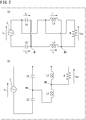
- FIG. 1 is a circuit diagram showing a transformer 1 as a basic form of a transformer according to the present embodiment.
- the transformer 1 is provided between an AC power supply 2 and a load R (R also denotes a resistance value).
- the transformer 1 includes a pair of capacitors C1 and C2, a pair of inductors L1 and L2, four switches S r1 , S r2 , S b1 , and S b2 , and a control section 3 which performs ON/OFF control of the switches S r1 , S r2 , S b1 , and S b2 .
- a switching frequency of the control section 3 is, for example, about 1 MHz.
- the pair of capacitors C1 and C2 may have the same capacitance value, or may have different capacitance values. The same applies to the inductance values of the pair of inductors L1 and L2.
- the switches S r1 , S r2 , S b1 , and S b2 and the control section 3 form a switch device 4 which switches the state of circuit connection of the transformer 1.
- the switches S r1 and S r2 operate in synchronization with each other, and the switches S b1 and S b2 operate in synchronization with each other.
- the pair of switches S r1 and S r2 and the pair of switches S b1 and S b2 operate so as to be alternately turned ON exclusively from each other.
- the switches S r1 , S r2 , S b1 , and S b2 are semiconductor switching elements formed by an SiC element or a GaN element, for example.
- the SiC element or the GaN element allows faster switching than an Si element, for example.
- sufficient withstand voltage (which can be even 6kV per element, for example) can be obtained without connecting multiple stages of such elements.
- the pair of capacitors C1 and C2 are connected in series to each other via a connection point M1.
- the AC power supply 2 is connected between both ends of this series unit.
- Input voltage v in is applied to the series unit of the pair of capacitors C1 and C2, so that input current i in flows.
- the pair of inductors L1 and L2 are connected in series to each other via a connection point M2. Between both ends of this series unit, input voltage v m is applied via the capacitors C1 and C2, so that current i m flows.
- input voltage v m is applied via the capacitors C1 and C2, so that current i m flows.
- one of the switches S r2 and S b2 is ON, current flows in the load R.
- voltage applied to the load R is V out
- output current flowing from the transformer 1 to the load R is i out .
- FIG. 2 (a) is a circuit diagram showing a substantial connection state when, among the four switches S r1 , S r2 , S b1 , and S b2 in FIG. 1 , the two switches S r1 and S r2 on the upper side are ON, and the two switches S b1 and S b2 on the lower side are OFF.
- the switch device 4 in FIG. 1 is not shown.
- (b) is a circuit diagram showing, in a step-like shape, the same circuit diagram as in (a).
- FIG. 3 (a) is a circuit diagram showing a substantial connection state when, among the four switches S r1 , S r2 , S b1 , and S b2 , the two switches S b1 and S b2 on the lower side are ON, and the two switches S r1 and S r2 on the upper side are OFF.
- (b) is a circuit diagram showing, in a step-like shape, the same circuit diagram as in (a).
- the circuit configuration is composed of a front stage circuit including the pair of capacitors C1 and C2, and a rear stage circuit including the pair of inductors L1 and L2, and at each stage, the polarity of output relative to input is inverted through switching.
- the capacitors C1 and C2 the directions of currents thereof are alternately inverted through switching.
- the inductors L1 and L2 the directions of voltages thereof are alternately inverted through switching.
- v in is input voltage from the AC power supply 2
- v out is voltage applied to the load R
- v 1 is voltage applied to the capacitor C1
- v 2 is voltage applied to the capacitor C2
- i 1 is current flowing through the inductor L1
- i 2 is current flowing through the inductor L2.
- v in is input voltage from the AC power supply 2
- v out is voltage applied to the load R
- v 1 is voltage applied to the capacitor C1
- v 2 is voltage applied to the capacitor C2
- i 1 is current flowing through the inductor L1
- i 2 is current flowing through the inductor L2.
- the second term on the right-hand side of the expression at the lowermost stage is sufficiently smaller than the first term, and thus can be neglected. Therefore, v in ⁇ 4v out is satisfied regardless of load variation (variation in the value of R), and output voltage becomes about 1/4 of input voltage. Since no loss occurs except for the load R, output current is about four times as great as input current, and input impedance is sixteen times as great as the resistance value R.
- a circuit parameter condition regarding inductance, 2 ⁇ tf o L ⁇ R is satisfied. In addition, regarding capacitance, 1/(2 ⁇ fsC) ⁇ R ⁇ 1/(2 ⁇ f o C) is satisfied. If this circuit parameter condition is satisfied, it is reliably realized that the voltage transformation ratio is constant regardless of load variation, and more stable transformation operation with less distortion is obtained.
- a difference represented by the inequality sign is, for example, one-digit difference or greater, or more preferably, two-digit difference or greater.
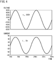
- FIG. 4 is a waveform diagram in which an upper graph shows input voltage to the transformer 1 and a lower graph shows input current to the transformer 1.
- FIG. 5 is a waveform diagram showing voltage v m and current i m at an intermediate stage of transformation. Actually, these are composed of pulse trains based on switching, and as a whole, have such waveforms as shown in FIG. 5 .
- FIG. 6 is a waveform diagram in which an upper graph shows output voltage from the transformer 1 and a lower graph shows output current from the transformer 1. As is obvious from comparison between FIG. 4 and FIG. 6 , voltage is transformed to be 1/4, and along with this, current is quadrupled.
- the transformer 1 shown in FIG. 1 is composed of a front stage circuit 1f including the switches S r1 and S b1 and the capacitors C1 and C2, and a rear stage circuit 1r including the switches S r2 and S b2 and the inductors L1 and L2.
- the circuit configurations of the front stage circuit 1f and the rear stage circuit 1r can be topologically expressed as follows.
- the front stage circuit 1f includes a “switch series unit” and “capacitors” described below.
- the "switch series unit” is composed of two switches (Sr1 and Sb1) connected in series to each other.
- the odd-numbered switch (S r1 ) and the even-numbered switch (S b1 ), as seen from one end (e.g., an upper end) of both ends of the series unit, are configured to be alternately turned ON, and the switch series unit as a whole is connected in parallel to the power supply 2.
- the “capacitors (C1 and C2)" are disposed on at least one electrical path of a first electrical path and a second electrical path.
- the first electrical path combines the odd nodes (N1 and N3) and leads the odd nodes to a first output port Px, while the second electrical path leads the even node (N2) to a second output port Py.
- the “capacitors (C1 and C2)" are present so as to correspond to two nodes.
- the rear stage circuit 1r includes an "element series unit” and “inductors” described below.
- the “element series unit” is composed of a pair of semiconductor elements (S r2 and S b2 ) that are connected in series to each other and perform conducting operations of mutually opposite polarities, and one of both ends of the series unit is connected to the first output port Px while the other end thereof is connected to the second output port Py.
- the “inductors (L1 and L2)" are disposed on at least one electrical path of a third electrical path and a fourth electrical path.
- the third electrical path combines two nodes (N11 and N13) that are points at the both ends of the element series unit, and leads the nodes to one of both ends of the load R.
- the fourth electrical path leads one node (N12) that is a mutual connection point of the pair of semiconductor elements to the other end of the load R.
- the “inductors (L1 and L2)" are present so as to correspond to two nodes (N11 and N13) among the three nodes in total.
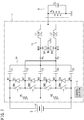
- FIG. 7 is a circuit diagram of such a transformer 1.
- This transformer 1 is provided between a power supply 2 and a load R, and is composed of a front stage circuit 1f, a rear stage circuit 1r, and a control section 3.
- the power supply 2 is a DC power supply
- voltage is 1 kV.
- the load R includes a resistance R 3 and a capacitance C 6 as equivalent circuit elements.
- the front stage circuit 1f includes bleeder resistor R1 and R2, switches SW1 to SW4, diodes D1 to D4 intrinsic to the switches SW1 to SW4, and capacitors C1 to C5, and these elements are connected as shown in FIG. 7 .
- the rear stage circuit 1r includes diodes D11 and D12 and inductors L1 and L2, and these elements are connected as shown in FIG. 7 .
- control section 3 which performs ON/OFF control of the switches SW1 to SW4 is provided.
- the diodes D1 to D4 may be body diodes intrinsic to the switches SW1 to SW4, or may be external diodes provided separately from the switches SW1 to SW4 depending on the type of the switches SW1 to SW4. These diodes D1 to D4 function as freewheel diodes, and may reduce switching loss, and further, may eventually reduce inductances of the inductors L1 and L2 and thus contribute to downsizing.
- the transformer 1 includes, as the front stage circuit 1f, a "switch series unit” and “capacitors (C1 to C5)”.
- the "switch series unit” is composed of the switches (SW1 to SW4) connected in series to each other.
- the odd-numbered switches (SW1 and SW3) and the even-numbered switches (SW2 and SW4), as seen from one end (e.g., an upper end) of both ends of the series unit, are alternately turned ON, and the switch series unit as a whole are connected in parallel to the power supply 2.
- the "capacitors (C1 to C5)" are disposed on at least one electrical path of a first electrical path and a second electrical path.
- the first electrical path combines the odd nodes (N1, N3, and N5) and leads the odd nodes to a first output port Px
- the second electrical path combines the even nodes (N2 and N4) and leads the even nodes to a second output port Py.
- the "capacitors (C1 to C5)” are present so as to correspond to five nodes.
- the transformer 1 includes, as the rear stage circuit 1r, an "element series unit” and “inductors (L1 and L2)".
- the “element series unit” is composed of a pair of semiconductor elements (D11 and D12) that are connected in series to each other, and perform conducting operations of mutually opposite polarities, and one of both ends of the series unit is connected to the first output port Px while the other end thereof is connected to the second output port Py.
- the “inductors (L1 and L2)" are disposed on at least one electrical path of a third electrical path and a fourth electrical path.
- the third electrical path combines two nodes (N11 and N13) that are points at the both ends of the element series unit, and leads the two nodes to one of both ends of the load R.
- the fourth electrical path leads one node (N12) that is a mutual connection point of the pair of semiconductor elements to the other end of the load R.
- the “inductors (L1 and L2)" are present so as to correspond to two nodes (N11 and N13) among the three nodes in total.
- the transformer shown in FIG. 7 performs switching so that the switches SW1 and SW3 and the switches SW2 and SW4 are alternately turned ON under the same conditions as those for the transformer 1 shown in FIG. 1 , and thus the transformer operates as a step-down circuit having a voltage transformation ratio of 1/8. That is, input voltage of 1 kV can be stepped down to DC voltage of 125 V.
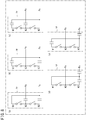
- FIG. 8 is a circuit diagram showing topological variations of a main part of the front stage circuit 1f in the "2C2L" transformer 1. Circuits shown in (a) to (e) of FIG. 9 are each composed of a pair of switches and a pair of capacitors (reference numerals thereof are omitted).
- capacitors are present so as to correspond to the node N3 of the switch series unit and the node N2 at the mutual connection point of the pair of switches.
- the topology of FIG. 1 is shown.
- capacitors are present so as to correspond to the node N1 of the switch series unit and the node N2 at the mutual connection point of the pair of switches.
- two capacitors are present so as to correspond to the node N3 of the switch series unit, and one capacitor is present in the output direction so as to correspond to the node N1.
- two capacitors are present so as to correspond to the node N1 of the switch series unit, and one capacitor is present in the output direction so as to correspond to the node N3.
- capacitors may be present so as to correspond to all the nodes N1 to N3.
- FIG. 9 is a circuit diagram showing topological variations of a main part of the rear stage circuit 1r.
- the rear stage circuit 1r connected to the load is composed of a pair of switches and a pair of inductors (reference numerals thereof are omitted). Instead of the switches, diodes may be used as shown in FIG. 7 .
- inductors are present so as to correspond to the node N13 of the switch series unit and the node N12 at the mutual connection point of the pair of switches.
- the topology of FIG. 1 is shown.
- inductors are present so as to correspond to the node N11 of the switch series unit and the node N12 at the mutual connection point of the pair of switches.
- two inductors are present so as to correspond to the node N13 of the switch series unit, and one inductor is present in the output direction so as to correspond to the node N11.
- two inductors are present so as to correspond to the node N11 of the switch series unit, and one inductor is present in the output direction so as to correspond to the node N13.
- inductors may be present so as to correspond to all the nodes N11 toN13.
- the inductances L (common inductance) of the two inductors L1 and L2 equally affect a dead time ⁇ described later.
- the inductance L1, of the inductances L 1 and L 2 of the two inductors L1 and L2 is dominant in setting of the dead time ⁇ .
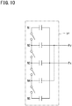
- FIG. 10 shows the main part of the front stage circuit 1f in the "4C2L" transformer 1.
- a first electrical path that combines the odd nodes N1, N3, and N5 as seen from one of both ends of the switch series unit and leads the odd nodes to the first output port Px is represented by a solid line
- a second electrical path that combines the even nodes N2 and N4 and leads the even nodes to the second output port Py is represented by a dashed line. Expressing the second electrical path by the dashed line is simply for convenience of illustration, and the second electrical path coexists with the first electrical path.
- This topology is identical to the front stage circuit 1f shown in FIG. 7 .
- At least one capacitor needs to be interposed between nodes that are mutually combined and connected by the first electrical path (solid line) or the second electrical path (dashed line) among the five nodes N1 to N5, in order to realize insulation for DC therebetween.
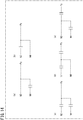
- FIG. 11 and FIG. 12 each show circuit variations of the first electrical path in the case where the total number of capacitors is not reduced in the first electrical path (solid line) shown in FIG. 10 .
- FIG. 13 is a diagram showing circuit variations of the first electrical path in the case where the total number of capacitors is reduced by one in the first electrical path (solid line) shown in FIG. 10 .
- one node among the nodes N1, N3, and N5 is directly connected to the first output port Px.
- the other nodes are each connected to the first output port Px via one capacitor or two capacitors.
- FIG. 14 is a diagram showing circuit variations of the second electrical path (dashed line) shown in FIG. 10 .
- (a) and (b) are circuit diagrams in the case where one capacitor is reduced in the second electrical path while no capacitor is reduced in the first electrical path.
- the node N2 is directly connected to the second output port Py.
- the node N4 is connected to the second output port Py via a capacitor.
- the node N4 is directly connected to the second output port Py.
- the node N2 is connected to the second output port Py via a capacitor.
- (c), (d), and (e) are circuit diagrams in the case where one capacitor is reduced in the first electrical path while no capacitor is reduced in the second electrical path.
- the nodes N2 and N4 are each connected to the second output port Py via one capacitor or two capacitors.
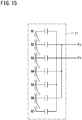
- FIG. 15 shows a main part of a front stage circuit 1f in a "6C2L" transformer 1.
- a first electrical path that combines odd nodes N1, N3, N5, and N7 as seen from one of both ends of the switch series unit and leads the odd nodes to the first output port Px is represented by a solid line
- a second electrical path that combines even nodes N2, N4, and N6 and leads the even nodes to the second output port Py is represented by a dashed line. Expressing the second electrical path by the dashed line is simply for convenience of illustration, and the second electrical path coexists with the first electrical path.
- At least one capacitor needs to be interposed between nodes that are mutually combined and connected by the first electrical path (solid line) or the second electrical path (dashed line) among the seven nodes N1 to N7, in order to realize insulation for DC therebetween.
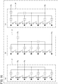
- FIG. 16 shows circuit variations in the case where one capacitor is reduced in the first electrical path (solid line) or the second electrical path (dashed line) shown in FIG. 15 .
- the node N3 is directly connected to the first output port Px without an interposed capacitor.
- the node N7 is directly connected to the first output port Px without an interposed capacitor.
- the node N4 is directly connected to the second output port Py without an interposed capacitor.
- front stage circuit 1f can be similarly extended to "8C" or more.
- the front stage circuit 1f can be topologically expressed as follows.
- the front stage circuit 1f includes: (a) a switch series unit composed of a plurality of switches, as many as a multiple of 2, connected in series to each other, the plurality of switches including odd-numbered switches and even-numbered switches as seen from one of both ends of the series unit, the odd-numbered switches and even-numbered switches being configured to be alternately turned ON, the switch series unit as a whole being connected in parallel to a power supply; and (b) assuming that mutual connection points of the respective switches and points at the both ends of the switch series unit are regarded as m nodes in total and the nodes are seen in order of 1 to m from one of the both ends of the switch series unit, capacitors provided on at least one electrical path of a first electrical path and a second electrical path, the first electrical path being configured to combine odd nodes and lead the odd nodes to a first output port, the second electrical path being configured to combine even nodes and lead the even nodes to a second output port,
- the rear stage circuit 1r includes: (c) an element series unit composed of a pair of semiconductor elements that are connected in series to each other and perform conducting operations of mutually opposite polarities, one of both ends of the series unit being connected to the first output port while the other end being connected to the second output port; and (d) inductors provided on at least one electrical path of a third electrical path and a fourth electrical path, the third electrical path being configured to combine two nodes that are points at the both ends of the element series unit and to lead the two nodes to one end of a load, the fourth electrical path being configured to lead one node that is a mutual connection point of the pair of semiconductor elements to the other end of the load, the inductors being present so as to correspond to at least two nodes of the three nodes in total.
- the element series unit can be configured by connecting the diodes in series with conducting directions thereof being opposite to each other. If the semiconductor elements are switches, the element series unit is configured by connecting a pair of switches in series, and the pair of switches are alternately turned ON.
- the transformer 1 as described above can perform transformation by the circuit configuration including the front stage circuit 1f and the rear stage circuit 1r and by switching.
- Using the transformer 1 as a power transformer makes it unnecessary to use a conventional transformer including a coil, an iron core, and the like. Therefore, it is possible to realize drastic size reduction and weight reduction of a transformer, and thereby realize cost reduction accordingly.
- problems of parasitic capacitance and occurrence of magnetic field leakage, which arise in a high-frequency transformer are also solved, and thus a transformer with low loss can be realized.
- the power supply either an AC power supply or a DC power supply is applicable.
- a dead time is a transient time from a moment when control for all switches is turned OFF to when control for either switches is turned on when, for example, the odd-numbered switches SW1 and SW3 and the even-numbered switches SW2 and SW4 shown in FIG. 7 are alternately turned ON.
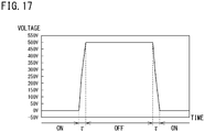
- FIG. 17 is a graph showing a change in switching voltage (drain-to-source voltage) when the odd-numbered switches or the even-numbered switches change from ON to OFF and then change to ON again.
- the switching voltage is 0 V.
- the switching voltage is 500 V, for example.
- ZVT zero voltage transition
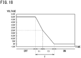
- FIG. 18 is a graph showing a part corresponding to the OFF to ON change shown in FIG. 17 , with the time on the horizontal axis being scaled up. It is found that, in FIG. 18 , the dead time ⁇ includes a first half time ⁇ 1 from 500 V to 250 V, and a subsequent second half time ⁇ 2 from 250 V to 0 V. That is, the following relationship is satisfied: ⁇ ⁇ ⁇ 1 + ⁇ 2
- the gradient of the first half time ⁇ 1 and the gradient of the second half time ⁇ 2 are slightly different from each other, and ⁇ 1 ⁇ ⁇ 2 is satisfied. Therefore, the dead time ⁇ can be considered separately for the first half time ⁇ 1 and the second half time ⁇ 2 . Assuming that the output voltage of 125 V from the transformer 1 is V out ,
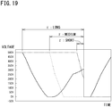
- FIG. 19 is a graph showing the relationship between ZVT and the length of the dead time which is set to be "long", “medium”, and “short”.
- the dead time ⁇ is shorter than an appropriate value (medium)
- a voltage change indicated by an alternate long and short dash line occurs, and next ON starts before the voltage reaches 0 V. That is, this is not ZVT.
- the dead time ⁇ is longer than the appropriate value (medium)
- a voltage change indicated by a solid line occurs and the voltage once reaches 0 V, but thereafter the voltage increases again, and eventually, next ON starts with the voltage remaining increased. That is, this is also not ZVT. Therefore, there is an appropriate (not too long and not too short) range of " ⁇ " indicated by the dashed line.
- FIG. 20 is a circuit diagram of a transformer 1 in which the diodes D1 to D4 and the bleeder resistors R1 and R2 shown in FIG. 7 are omitted, and instead, floating capacitances C11 to C14 possessed by the respective switches SW1 to SW4 are shown.
- FIG. 20 also shows a current path in the first half time ⁇ 1 . Of the diodes D11 and D12, the diode D12 is in the conductive state. At this time, current I L1 that flows in the inductor L1 flows into the floating capacitances C11 to C14.
- FIG. 21 is of the same background as FIG. 20 , FIG. 21 also shows a current path in the second half time ⁇ 2 .
- the diode D11 is in the conductive state.
- current I L2 that flows in the inductor L2 flows into the floating capacitances C11 to C14.
- FIG. 22 is a graph showing examples of waveforms of currents that flow in the inductors L1 and L2.
- the current waveforms can be approximated by straight lines as shown in FIG. 22 .
- the upper waveform is the waveform of I L1
- the lower waveform is the waveform of I L2 .
- a transition time from a minimum value to a maximum value of each waveform is half the switching cycle T.
- the voltage waveform at both ends of each of the inductors L1 and L2 is a rectangular wave having a duty ratio of 50%.
- V L1 and V L2 at both ends of the inductors L1 and L2, respectively, are the output voltage. That is, assuming that the maximum value of voltage V L is V Lmax and the minimum value of voltage V L is V Lmin , the following relationships are satisfied: V Lmax ⁇ V out V Lmin ⁇ ⁇ V out For simplifying calculation, V L 1 ⁇ V 12 ⁇ ⁇ V out .
- I Lp ⁇ p a T / 2 and therefore, the following relationship is satisfied.
- I Lp ⁇ p T ⁇ V out / 2 L
- FIG. 23 is an enlarged view showing a portion near the peaks of the waveforms shown in FIG. 22 .
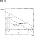
- FIG. 24 is a diagram showing the waveforms shown in FIG. 23 extended in the time-axis direction (rightward direction).
- the dead time ⁇ must be set so as not to reach time t 0 .
- the maximum value of the dead time that does not reach t 0 is referred to as ⁇ max .
- ⁇ max must satisfy ⁇ max ⁇ (T/2) in order to secure ON time of switching.
- the control section 3 of the transformer 1 after the time at which the dead time has started, obtains: the first half time ⁇ 1 which can be calculated on the basis of the electric charges that move from the inductor L1 to the floating capacitance C DS of the switch while one (D12) of the diodes D11 and D12 is in the conductive state; and the second half time ⁇ 2 which can be calculated on the basis of the electric charges that move from the inductor L2 to the floating capacitance C DS of the switch while one (D11) of the diodes D11 and D12 is in the conductive state, and then the control section 3 can determine the dead time ⁇ on the basis of the first half time ⁇ 1 and the second half time ⁇ 2 .
- an appropriate dead time ⁇ can be determined to realize zero voltage transition (ZVT).
- control section 3 terminates the dead time ⁇ before the electric charges that have moved to the floating capacitance C DS return to the inductors L1 and L2, thereby preventing the switching voltage from increasing again.
- the appropriate range of the dead time ⁇ can be precisely determined on the basis of the above expressions (15) to (17), thereby reliably realizing zero voltage transition.
- the minimum value and the maximum value of the dead time ⁇ are calculated as follows on the basis of above expressions (15) and (17).
- FIG. 25 is a graph showing the relationship between the dead time ⁇ [ns] and efficiency [%] in the case of the condition 1.
- ⁇ min and ⁇ max are plotted on the graph, it is found that these values correspond to a range in which the efficiency is excellent on the characteristics shown in the graph.
- FIG. 26 is a graph showing the relationship between the dead time ⁇ [ns] and output power [W] of the transformer in the case of the condition 1.
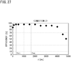
- FIG. 27 is a graph showing the relationship between the dead time ⁇ [ns] and efficiency [%] in the case of the condition 2.
- ⁇ min and ⁇ max are plotted on the graph, it is found that these values correspond to a range in which the efficiency is excellent on the characteristics shown in the graph.
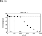
- FIG. 28 is a graph showing the relationship between the dead time ⁇ [ns] and output power [W] of the transformer in the case of the condition 2.
- ⁇ min and ⁇ max are plotted on the graph, it is found that these values correspond to a range in which stable high output is achieved on the characteristics shown in the graph.
- the minimum value and the maximum value of the dead time ⁇ are calculated as follows on the basis of expressions (15) and (17).
- FIG. 29 is a graph showing the relationship between the dead time ⁇ [ns] and efficiency [%] in the case of the condition 3.
- ⁇ min and ⁇ max are plotted on the graph, it is found that these values correspond to a range in which the efficiency is excellent on the characteristics shown in the graph.
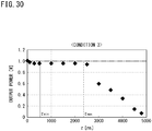
- FIG. 30 is a graph showing the relationship between the dead time ⁇ [ns] and output power [W] of the transformer in the case of the condition 3.
- ⁇ min and ⁇ max are plotted on the graph, it is found that these values correspond to a range in which stable high output is achieved on the characteristics shown in the graph.
- FIG. 31 is a graph showing the relationship between the dead time ⁇ [ns] and efficiency [%] in the case of the condition 4.
- ⁇ min and ⁇ max are plotted on the graph, it is found that these values correspond to a range in which the efficiency is excellent on the characteristics shown in the graph.
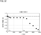
- FIG. 32 is a graph showing the relationship between the dead time ⁇ [ns] and output power [W] of the transformer in the case of the condition 4.
- ⁇ min and ⁇ max are plotted on the graph, it is found that these values correspond to a range in which stable high output is achieved on the characteristics shown in the graph.
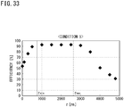
- FIG. 33 is a graph showing the relationship between the dead time ⁇ [ns] and efficiency [%] in the case of the condition 5.
- ⁇ min and ⁇ max are plotted on the graph, it is found that these values correspond to a range in which the efficiency is excellent on the characteristics shown in the graph.
- FIG. 34 is a graph showing the relationship between the dead time ⁇ [ns] and output power [W] of the transformer in the case of the condition 5.
- ⁇ min and ⁇ max are plotted on the graph, it is found that these values correspond to a range in which stable high output is achieved on the characteristics shown in the graph.
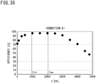
- FIG. 35 is a graph showing the relationship between the dead time ⁇ [ns] and efficiency [%] in the case of the condition 6.
- ⁇ min and ⁇ max are plotted on the graph, it is found that these values correspond to a range in which the efficiency is excellent on the characteristics shown in the graph.
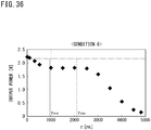
- FIG. 36 is a graph showing the relationship between the dead time ⁇ [ns] and output power [W] of the transformer in the case of the condition 6.
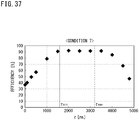
- FIG. 37 is a graph showing the relationship between the dead time ⁇ [ns] and efficiency [%] in the case of the condition 7.
- ⁇ min and ⁇ max are plotted on the graph, it is found that these values correspond to a range in which the efficiency is excellent on the characteristics shown in the graph.
- FIG. 38 is a graph showing the relationship between the dead time ⁇ [ns] and output power [W] of the transformer in the case of the condition 7.
- ⁇ min and ⁇ max are plotted on the graph, it is found that these values correspond to a range in which stable high output is achieved on the characteristics shown in the graph.
- the minimum value and the maximum value of the dead time ⁇ are calculated as follows on the basis of expressions (15) and (17).
- FIG. 39 is a graph showing the relationship between the dead time ⁇ [ns] and efficiency [%] in the case of the condition 8.
- ⁇ min and ⁇ max are plotted on the graph, it is found that these values correspond to a range in which the efficiency is excellent on the characteristics shown in the graph.
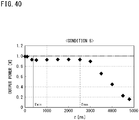
- FIG. 40 is a graph showing the relationship between the dead time ⁇ [ns] and output power [W] of the transformer in the case of the condition 8.
- ⁇ min and ⁇ max are plotted on the graph, it is found that these values correspond to a range in which stable high output is achieved on the characteristics shown in the graph.
- the value of the floating capacitance C DS is common among a plurality of capacitors.
- a case where a plurality of capacitors have different floating capacitances C DS will be verified.
- FIG. 41 is a graph showing the relationship between the dead time ⁇ [ns] and efficiency [%] in the case of the condition 9.
- ⁇ min and ⁇ max are plotted on the graph, it is found that these values correspond to a range in which the efficiency is excellent on the characteristics shown in the graph.
- FIG. 42 is a graph showing the relationship between the dead time ⁇ [ns] and output power [W] of the transformer in the case of the condition 9.
- ⁇ min and ⁇ max are plotted on the graph, it is found that these values correspond to a range in which stable high output is achieved on the characteristics shown in the graph.
- the minimum value and the maximum value of the dead time ⁇ are calculated as follows on the basis of expressions (15) and (17).
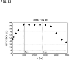
- FIG. 43 is a graph showing the relationship between the dead time ⁇ [ns] and efficiency [%] in the case of the condition 10.
- ⁇ min and ⁇ max are plotted on the graph, it is found that these values correspond to a range in which the efficiency is excellent on the characteristics shown in the graph.
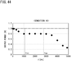
- FIG. 44 is a graph showing the relationship between the dead time ⁇ [ns] and output power [W] of the transformer in the case of the condition 10.
- the transformer can achieve excellent efficiency and stable high output.
Landscapes
- Engineering & Computer Science (AREA)
- Power Engineering (AREA)
- Inverter Devices (AREA)
- Dc-Dc Converters (AREA)
- Ac-Ac Conversion (AREA)
Abstract
Description
- The present invention relates to a transformer.
- In a commercial AC transmission and distribution system, a transformer is used. Just near a consumer's house, a pole transformer is used which transforms, for example, 6600 V (50 Hz or 60 Hz) to 200 V (see NON PATENT LITERATURE 1). Such a pole transformer has a thick coil as a conductive wire wound around an iron core, and therefore has a considerable weight. For example, a pole transformer with a diameter of 40 cm and a height of 80 cm has a weight of about 200 kg, including an insulating oil and a case.
- On the other hand, for realizing a smart grid which is a next-generation power system, studies of an SST (Solid-State Transformer) are being conducted. For the SST, a high-frequency transformer is used (for example, see NON PATENT LITERATURE 2).
- In recent years, there is a demand that, for example, output voltage (DC) of photovoltaic generation is stepped down to be used for a low-voltage power supply for measurement. There are cases where the output voltage of photovoltaic generation is as high as 1000 V. In order to step down such high voltage to about 100 to 200 V, an intervening device such as a step-down transformer is needed as in an AC circuit.
-
- NON PATENT LITERATURE 1: Homepage of Chubu Electric Power Co., Inc., [Pole Transformer], [online], [searched on September 12, 2014], Internet <URL:http://www.chuden.co.jp/kids/kids_denki/home/hom_kaku/index.html>
- NON PATENT LITERATURE 2: Falcones, S.: et al., Power and Energy Society General Meeting, 2010 IEEE, pp. 1-8, Minneapolis, July 2010
- The conventional pole transformer is heavy, and therefore is not easy to handle. In addition, an attachment space that is large enough to contain the outer dimension of the transformer is needed on the pole.
- On the other hand, the high-frequency transformer cannot avoid an influence of a parasitic capacitance, and has a difficulty in designing.
- Considering such conventional problems, an object of the present invention is to provide an innovative next-generation transformer with a small size and a light weight, which does not need a coil, an iron core, and the like for magnetic coupling, electromagnetic induction, or mutual inductance as used in the conventional transformer. Either an AC power supply or a DC power supply may be used.
- A transformer according to the present invention is provided between a power supply and a load, and composed of a front stage circuit and a rear stage circuit. The transformer includes, as the front stage circuit, (a) a switch series unit composed of a plurality of switches, as many as a multiple of 2, connected in series with each other, the plurality of switches including odd-numbered switches and even-numbered switches as seen from one of both ends of the series unit, the odd-numbered switches and the even-numbered switches being configured to be alternately turned ON, the switch series unit as a whole being connected in parallel to the power supply, and (b) assuming that mutual connection points of the respective switches and points at the both ends of the switch series unit are regarded as m nodes in total and the nodes are seen in order of 1 to m from one of the both ends of the switch series unit, capacitors provided on at least one electrical path of a first electrical path and a second electrical path, the first electrical path being configured to combine odd nodes and lead the odd nodes to a first output port, the second electrical path being configured to combine even nodes and lead the even nodes to a second output port, the capacitors being present so as to correspond to at least (m - 1) nodes. The transformer includes, as the rear stage circuit, (c) an element series unit composed of a pair of semiconductor elements that are connected in series to each other and perform conducting operations of mutually opposite polarities, one of both ends of the element series unit being connected to the first output port while the other end thereof being connected to the second output port, and (d) inductors provided on at least one electrical path of a third electrical path and a fourth electrical path, the third electrical path being configured to combine two nodes that are points at the both ends of the element series unit and to lead the two nodes to one of both ends of the load, the fourth electrical path being configured to lead one node that is a mutual connection point of the pair of semiconductor elements to the other end of the load, the inductors being present so as to correspond to at least two nodes of the three nodes in total. The transformer further includes a control section configured to control ON/OFF operations of the switches.
- According to the transformer of the present invention, it is possible to provide an innovative next-generation transformer with a small size and a light weight, which does not need a coil, an iron core, and the like for magnetic coupling, electromagnetic induction, or mutual inductance as used in the conventional transformer.
-
- [
FIG. 1] FIG. 1 is a circuit diagram showing a transformer as a basic form of a transformer according to an embodiment. - [
FIG. 2] FIG. 2 is a circuit diagram in which (a) shows a substantial connection state when, of four switches shown inFIG. 1 , two switches on the upper side are ON and two switches on the lower side are OFF, and (b) shows, in a step-like shape, the same circuit diagram as in (a). - [
FIG. 3] FIG. 3 is a circuit diagram in which (a) shows a substantial connection state when, of four switches shown inFIG. 1 , two switches on the lower side are ON and two switches on the upper side are OFF, and (b) shows, in a step-like shape, the same circuit diagram as in (a). - [
FIG. 4] FIG. 4 is a waveform diagram in which an upper graph shows input voltage to the transformer and a lower graph shows input current to the transformer. - [
FIG. 5] FIG. 5 is a waveform diagram showing voltage Vm and current im at an intermediate stage of transformation. - [
FIG. 6] FIG. 6 is a waveform diagram in which an upper graph shows output voltage from the transformer and a lower graph shows output current from the transformer. - [
FIG. 7] FIG. 7 is a circuit diagram showing an example of a transformer that is developed to be more practical. - [
FIG. 8] FIG. 8 is a circuit diagram showing topological variations of a main part of a front stage circuit in a "2C2L" transformer. - [
FIG. 9] FIG. 9 is a circuit diagram showing topological variations of a main part of a rear stage circuit. - [
FIG. 10] FIG. 10 is a diagram showing a main part of a front stage circuit in a "4C2L" transformer. - [
FIG. 11] FIG. 11 is a diagram showing circuit variations of a first electrical path in a case where the total number of capacitors is not reduced in the first electrical path (solid line). - [
FIG. 12] FIG. 12 is a diagram showing other circuit variations of the first electrical path in a case where the total number of capacitors is not reduced in the first electrical path (solid line). - [
FIG. 13] FIG. 13 is a diagram showing circuit variations of the first electrical path in a case where the total number of capacitors is reduced by one in the first electrical path (solid line) shown inFIG. 10 . - [
FIG. 14] FIG. 14 is a diagram showing circuit variations of a second electrical path (dashed line) shown inFIG. 10 . - [
FIG. 15] FIG. 15 is a diagram showing a main part of a front stage circuit in a "6C2L" transformer. - [
FIG. 16] FIG. 16 is a diagram showing circuit variations in a case where the total number of capacitors are reduced by one in the first electrical path (solid line) or the second electrical path (dashed line) shown inFIG. 15 . - [
FIG. 17] FIG. 17 is a graph showing a change in switching voltage (drain-to-source voltage) when odd-numbered or even-numbered switches change from ON to OFF and change to ON again. - [
FIG. 18] FIG. 18 is a graph showing the change from OFF to ON shown inFIG. 17 , with the time on the horizontal axis being scaled up. - [
FIG. 19] FIG. 19 is a graph showing the relationship between ZVT and the length of dead time which is set to be "long", "medium", and "short". - [
FIG. 20] FIG. 20 is a circuit diagram in which diodes and bleeder resistors shown inFIG. 7 are omitted, and instead, floating capacitances possessed by the respective switches are shown. - [
FIG. 21] FIG. 21 is a circuit diagram of the same background asFIG. 20 , in which a path of current in a second half time τ2 is also shown. - [
FIG. 22] FIG. 22 is a graph showing examples of waveforms of currents that flow in inductors. - [
FIG. 23] FIG. 23 is an enlarged view showing portions near the peaks of the waveforms shown inFIG. 22 . - [
FIG. 24] FIG. 24 is a diagram showing the waveforms shown inFIG. 23 extended in the time-axis direction (rightward direction). - [
FIG. 25] FIG. 25 is a graph showing the relationship between dead time τ [ns] and efficiency [%] in the case ofcondition 1. - [
FIG. 26] FIG. 26 is a graph showing the relationship between dead time τ [ns] and output power [W] of the transformer in the case ofcondition 1. - [
FIG. 27] FIG. 27 is a graph showing the relationship between dead time τ [ns] and efficiency [%] in the case ofcondition 2. - [
FIG. 28] FIG. 28 is a graph showing the relationship between dead time τ [ns] and output power [W] of the transformer in the case ofcondition 2. - [
FIG. 29] FIG. 29 is a graph showing the relationship between dead time τ [ns] and efficiency [%] in the case ofcondition 3. - [
FIG. 30] FIG. 30 is a graph showing the relationship between dead time τ [ns] and output power [W] of the transformer in the case ofcondition 3. - [
FIG. 31] FIG. 31 is a graph showing the relationship between dead time τ [ns] and efficiency [%] in the case ofcondition 4. - [
FIG. 32] FIG. 32 is a graph showing the relationship between dead time τ [ns] and output power [W] of the transformer in the case ofcondition 4. - [
FIG. 33] FIG. 33 is a graph showing the relationship between dead time τ [ns] and efficiency [%] in the case ofcondition 5. - [
FIG. 34] FIG. 34 is a graph showing the relationship between dead time τ [ns] and output power [W] of the transformer in the case ofcondition 5. - [
FIG. 35] FIG. 35 is a graph showing the relationship between dead time τ [ns] and efficiency [%] in the case ofcondition 6. - [
FIG. 36] FIG. 36 is a graph showing the relationship between dead time τ [ns] and output power [W] of the transformer in the case ofcondition 6. - [
FIG. 37] FIG. 37 is a graph showing the relationship between dead time τ [ns] and efficiency [%] in the case ofcondition 7. - [
FIG. 38] FIG. 38 is a graph showing the relationship between dead time τ [ns] and output power [W] of the transformer in the case ofcondition 7. - [
FIG. 39] FIG. 39 is a graph showing the relationship between dead time τ [ns] and efficiency [%] in the case ofcondition 8. - [
FIG. 40] FIG. 40 is a graph showing the relationship between dead time τ [ns] and output power [W] of the transformer in the case ofcondition 8. - [
FIG. 41] FIG. 41 is a graph showing the relationship between dead time τ [ns] and efficiency [%] in the case ofcondition 9. - [
FIG. 42] FIG. 42 is a graph showing the relationship between dead time τ [ns] and output power [W] of the transformer in the case ofcondition 9. - [
FIG. 43] FIG. 43 is a graph showing the relationship between dead time τ [ns] and efficiency [%] in the case ofcondition 10. - [
FIG. 44] FIG. 44 is a graph showing the relationship between dead time τ [ns] and output power [W] of the transformer in the case ofcondition 10. - The summary of the embodiment of the present invention includes at least the following.
- (1) A transformer provided between a power supply and a load is composed of a front stage circuit and a rear stage circuit.
The transformer includes, as the front stage circuit, (a) a switch series unit composed of a plurality of switches, as many as a multiple of 2, connected in series with each other, the plurality of switches including odd-numbered switches and even-numbered switches as seen from one of both ends of the series unit, the odd-numbered switches and the even-numbered switches being configured to be alternately turned ON, the switch series unit as a whole being connected in parallel to the power supply, and (b) assuming that mutual connection points of the respective switches and points at the both ends of the switch series unit are regarded as m nodes in total and the nodes are seen in order of 1 to m from one of the both ends of the switch series unit, capacitors provided on at least one electrical path of a first electrical path and a second electrical path, the first electrical path being configured to combine odd nodes and lead the odd nodes to a first output port, the second electrical path being configured to combine even nodes and lead the even nodes to a second output port, the capacitors being present so as to correspond to at least (m - 1) nodes. The capacitors are present so as to correspond to at least (m - 1) nodes.
In addition, the transformer includes, as the rear stage circuit, (c) an element series unit composed of a pair of semiconductor elements that are connected in series to each other and perform conducting operations of mutually opposite polarities, one of both ends of the element series unit being connected to the first output port while the other end thereof being connected to the second output port, and (d) inductors provided on at least one electrical path of a third electrical path and a fourth electrical path, the third electrical path being configured to combine two nodes that are points at the both ends of the element series unit and to lead the two nodes to one of both ends of the load, the fourth electrical path being configured to lead one node that is a mutual connection point of the pair of semiconductor elements to the other end of the load. The inductors are present so as to correspond to at least two nodes of the three nodes in total.
The transformer further includes a control section configured to control ON/OFF operations of the switches.
The transformer configured as described in above (1) can perform transformation by the circuit configuration including the front stage circuit and the rear stage circuit and by switching. Using this transformer as a power transformer makes it unnecessary to use a conventional transformer including a coil, an iron core, and the like. Therefore, it is possible to realize drastic size reduction and weight reduction of the transformer, and thereby realize cost reduction accordingly. In addition, problems of parasitic capacitance and occurrence of magnetic field leakage, which arise in a high-frequency transformer, are also solved, and thus a transformer with low loss can be realized. As for a power supply, either an AC power supply or a DC power supply is applicable. - (2) Further, in the transformer described in the above (1), it is assumed that a time period from a dead-time start time to a dead-time end time is a dead time τ, the dead-time start time being a time at which control for the odd-numbered switches and control for the even-numbered switches are both turned OFF, the dead-time end time being a time at which control for either the odd-numbered switches or the even-numbered switches is turned ON. In this case, the control section, after the dead-time start time, may calculate a first half time τ1 and a second half time τ2, the first half time τ1 being calculated on the basis of electric charges that move from the inductors to floating capacitances of the switches while one of the semiconductor elements is in a conductive state, the second half time τ2 being calculated on the basis of electric charges that move from the inductors to the floating capacitances of the switches while the other semiconductor element is in a conductive state, and the control section may determine the dead time τ on the basis of the first half time τ1 and the second half time τ2.
In this case, an appropriate dead time τ can be determined on the basis of the times τ1 and τ2 calculated focusing on movement of electric charges during the dead time, thereby realizing zero volt transition (ZVT). - (3) Further, in the transformer described in the above (2), the control section preferably terminates the dead time τ before the electric charges that have moved to the floating capacitances return to the inductors.
When the electric charges that have moved to the floating capacitances return, switching voltage increases again. However, by terminating the dead time τ before the returning of the electric charges, the switching voltage can be prevented from increasing again. - (4) Further, in the transformer as described in the above (3), assuming that a switching cycle of the switches is T, an inductance of the inductors is L, and a resistance value of the load is R3, the dead time τ satisfies the following relationship:

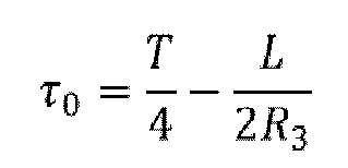


In this case, an optimum range of the dead time τ can be precisely determined, thereby reliably realizing zero voltage transition. - (5) Depending on the topology of the rear stage circuit, the following configuration may be taken instead of the above (4).
- Assuming that a switching cycle of the switches is T, an inductance, of the inductances of the inductors, that is dominant for the dead time is L1, and a resistance value of the load is R3, the dead time τ satisfies the following relationship:


- Hereinafter, an embodiment will be described in detail with reference to the drawings.
-
FIG. 1 is a circuit diagram showing atransformer 1 as a basic form of a transformer according to the present embodiment. InFIG. 1 , thetransformer 1 is provided between anAC power supply 2 and a load R (R also denotes a resistance value). Thetransformer 1 includes a pair of capacitors C1 and C2, a pair of inductors L1 and L2, four switches Sr1, Sr2, Sb1, and Sb2, and acontrol section 3 which performs ON/OFF control of the switches Sr1, Sr2, Sb1, and Sb2. A switching frequency of thecontrol section 3 is, for example, about 1 MHz. - The pair of capacitors C1 and C2 may have the same capacitance value, or may have different capacitance values. The same applies to the inductance values of the pair of inductors L1 and L2.
- The switches Sr1, Sr2, Sb1, and Sb2 and the
control section 3 form aswitch device 4 which switches the state of circuit connection of thetransformer 1. The switches Sr1 and Sr2 operate in synchronization with each other, and the switches Sb1 and Sb2 operate in synchronization with each other. The pair of switches Sr1 and Sr2 and the pair of switches Sb1 and Sb2 operate so as to be alternately turned ON exclusively from each other. The switches Sr1, Sr2, Sb1, and Sb2 are semiconductor switching elements formed by an SiC element or a GaN element, for example. The SiC element or the GaN element allows faster switching than an Si element, for example. In addition, sufficient withstand voltage (which can be even 6kV per element, for example) can be obtained without connecting multiple stages of such elements. - In
FIG. 1 , the pair of capacitors C1 and C2 are connected in series to each other via a connection point M1. TheAC power supply 2 is connected between both ends of this series unit. Input voltage vin is applied to the series unit of the pair of capacitors C1 and C2, so that input current iin flows. - The pair of inductors L1 and L2 are connected in series to each other via a connection point M2. Between both ends of this series unit, input voltage vm is applied via the capacitors C1 and C2, so that current im flows. When one of the switches Sr2 and Sb2 is ON, current flows in the load R. Here, voltage applied to the load R is Vout, and output current flowing from the
transformer 1 to the load R is iout. - In
FIG. 2 , (a) is a circuit diagram showing a substantial connection state when, among the four switches Sr1, Sr2, Sb1, and Sb2 inFIG. 1 , the two switches Sr1 and Sr2 on the upper side are ON, and the two switches Sb1 and Sb2 on the lower side are OFF. In the drawing, theswitch device 4 inFIG. 1 is not shown. InFIG. 2 , (b) is a circuit diagram showing, in a step-like shape, the same circuit diagram as in (a). - On the other hand, in
FIG. 3 , (a) is a circuit diagram showing a substantial connection state when, among the four switches Sr1, Sr2, Sb1, and Sb2, the two switches Sb1 and Sb2 on the lower side are ON, and the two switches Sr1 and Sr2 on the upper side are OFF. InFIG. 3 , (b) is a circuit diagram showing, in a step-like shape, the same circuit diagram as in (a). - While the states shown in
FIG. 2 andFIG. 3 are alternately repeated, voltage obtained via the connection point M1 of the series unit of the capacitors C1 and C2 becomes voltage obtained via the connection point M2 of the series unit of the inductors L1 and L2. That is, the circuit configuration is composed of a front stage circuit including the pair of capacitors C1 and C2, and a rear stage circuit including the pair of inductors L1 and L2, and at each stage, the polarity of output relative to input is inverted through switching. Regarding the capacitors C1 and C2, the directions of currents thereof are alternately inverted through switching. Regarding the inductors L1 and L2, the directions of voltages thereof are alternately inverted through switching. - Here, it can be estimated that the input voltage becomes 1/4 when outputted. This will be logically proved below.
- In
FIG. 2 , vin is input voltage from theAC power supply 2, vout is voltage applied to the load R, v1 is voltage applied to the capacitor C1, v2 is voltage applied to the capacitor C2, i1 is current flowing through the inductor L1, and i2 is current flowing through the inductor L2. In this case, the following expressions are satisfied. - For simplifying calculation, it is assumed that the capacitors C1 and C2 have the same capacitance value C, and the inductors L1 and L2 have the same inductance value L.


- The above expressions are converted into expressions of v1, i1, and i2, as follows.


- Here, if Ri1 = v3 and Ri2 = v4 are set, the following
equation 1 is obtained.
- In
FIG. 3 , as inFIG. 2 , vin is input voltage from theAC power supply 2, vout is voltage applied to the load R, v1 is voltage applied to the capacitor C1, v2 is voltage applied to the capacitor C2, i1 is current flowing through the inductor L1, and i2 is current flowing through the inductor L2. In this case, the following expressions are satisfied.


- The above expressions are converted into expressions of v1, i1, and i2, as follows.


- Here, if Ri1 = v3 and Ri2 = v4 are set, the following
equation 2 is obtained.
- Here, it is difficult to derive an exact solution from the above two states. Therefore, the following conditions are set within a range that is considered to cause no practical problem.
- (1) At a frequency fo of input voltage, the impedance (reactance) of L is sufficiently smaller than the resistance value. That is, 2πfoL << R is satisfied. Preferably, a difference represented by the inequality sign is, for example, one-digit difference or greater, or more preferably, two-digit difference or greater. Thus, more stable transformation operation with less distortion can be obtained.
- (2) At the switching frequency fs, the impedance (reactance) of C is sufficiently smaller than the resistance value R, but at the frequency fo of input voltage, the impedance (reactance) of C is sufficiently greater than the resistance value. That is, 1/(2πfsC) << R << 1/(2πfoC) is satisfied. Preferably, a difference represented by the inequality sign is, for example, one-digit difference or greater, or more preferably, two-digit difference or greater. Thus, more stable transformation operation with less distortion can be obtained.
- (3) In one cycle of switching, input voltage hardly varies.
Therefore, vin(t + Δt) = vin(t) (0 ≤ Δt ≤ 1/fs) - (4) The system is steady, and returns to the same state with a period (1/fs). Therefore, vx(t + (1/fs)) ≈ vx(t) (x = 1, 2, 3, 4)
- If the switches Sr1 and Sr2 become ON during a period of 0 ≤ t ≤ (1/2fs) and the switches Sb1 and Sb2 become ON during a period of (1/2fs) ≤ t≤ (1/fs), the following
equation 3 is obtained by primary approximation ofequation 1 about t = 0. In addition, the followingequation 4 is obtained by primary approximation ofequation 2 about t = (1/2fs).
- In the
above equation 3, the third term on the right-hand side of the expression at the third stage, i.e., - (1/2){vin(1/2fs) - vin(0)} is sufficiently close to zero.
- In the
above equation 4, the third term on the right-hand side of the expression at the third stage, i.e., - (1/2){vin(1/fs) - vin(1/2fs)} is sufficiently close to zero. - Here, if v1, v3, and v4 in
equations 


- If a sum of the expressions at the first and second stages shown above (just above) is taken, the following expression is obtained.

- Here, from the expression at the third stage in
equation 3, v1(0) - v1(ΔT) = (1/(4fsCR))v4(0) is obtained. - In addition, - vout = R(i1 + i2) = v3 + v4 is obtained, and this expression is always satisfied. Therefore, the following conclusive expression is obtained.

- Here, for simplification, it has been assumed that the values C are the same value and the values L are the same value. However, even if these values are different values, the same result can be derived through similar expression development.
- In the conclusive expression, the second term on the right-hand side of the expression at the lowermost stage is sufficiently smaller than the first term, and thus can be neglected. Therefore, vin ≈ 4vout is satisfied regardless of load variation (variation in the value of R), and output voltage becomes about 1/4 of input voltage. Since no loss occurs except for the load R, output current is about four times as great as input current, and input impedance is sixteen times as great as the resistance value R.
- As a circuit parameter condition, regarding inductance, 2πtfoL << R is satisfied. In addition, regarding capacitance, 1/(2πfsC) << R << 1/(2πfoC) is satisfied. If this circuit parameter condition is satisfied, it is reliably realized that the voltage transformation ratio is constant regardless of load variation, and more stable transformation operation with less distortion is obtained. Preferably, a difference represented by the inequality sign is, for example, one-digit difference or greater, or more preferably, two-digit difference or greater.
-
FIG. 4 is a waveform diagram in which an upper graph shows input voltage to thetransformer 1 and a lower graph shows input current to thetransformer 1. -
FIG. 5 is a waveform diagram showing voltage vm and current im at an intermediate stage of transformation. Actually, these are composed of pulse trains based on switching, and as a whole, have such waveforms as shown inFIG. 5 . -
FIG. 6 is a waveform diagram in which an upper graph shows output voltage from thetransformer 1 and a lower graph shows output current from thetransformer 1. As is obvious from comparison betweenFIG. 4 andFIG. 6 , voltage is transformed to be 1/4, and along with this, current is quadrupled. - The
transformer 1 shown inFIG. 1 is composed of afront stage circuit 1f including the switches Sr1 and Sb1 and the capacitors C1 and C2, and arear stage circuit 1r including the switches Sr2 and Sb2 and the inductors L1 and L2. The circuit configurations of thefront stage circuit 1f and therear stage circuit 1r can be topologically expressed as follows. - That is, the
front stage circuit 1f includes a "switch series unit" and "capacitors" described below. - The "switch series unit" is composed of two switches (Sr1 and Sb1) connected in series to each other. The odd-numbered switch (Sr1) and the even-numbered switch (Sb1), as seen from one end (e.g., an upper end) of both ends of the series unit, are configured to be alternately turned ON, and the switch series unit as a whole is connected in parallel to the
power supply 2. - When a mutual connection point (N2) of the respective switches and points (N1 and N3) at the both ends of the switch series unit are regarded as three nodes in total and these three nodes are seen in order of 1 to 3 from one of the both ends of the switch series unit, the "capacitors (C1 and C2)" are disposed on at least one electrical path of a first electrical path and a second electrical path. The first electrical path combines the odd nodes (N1 and N3) and leads the odd nodes to a first output port Px, while the second electrical path leads the even node (N2) to a second output port Py. The "capacitors (C1 and C2)" are present so as to correspond to two nodes.
- The
rear stage circuit 1r includes an "element series unit" and "inductors" described below. - The "element series unit" is composed of a pair of semiconductor elements (Sr2 and Sb2) that are connected in series to each other and perform conducting operations of mutually opposite polarities, and one of both ends of the series unit is connected to the first output port Px while the other end thereof is connected to the second output port Py.
- The "inductors (L1 and L2)" are disposed on at least one electrical path of a third electrical path and a fourth electrical path. The third electrical path combines two nodes (N11 and N13) that are points at the both ends of the element series unit, and leads the nodes to one of both ends of the load R. The fourth electrical path leads one node (N12) that is a mutual connection point of the pair of semiconductor elements to the other end of the load R. The "inductors (L1 and L2)" are present so as to correspond to two nodes (N11 and N13) among the three nodes in total.
- Next, an example of a transformer obtained by practically developing the above-described basic circuit will be described on the basis of the basic circuit.
-
FIG. 7 is a circuit diagram of such atransformer 1. Thistransformer 1 is provided between apower supply 2 and a load R, and is composed of afront stage circuit 1f, arear stage circuit 1r, and acontrol section 3. For example, thepower supply 2 is a DC power supply, and voltage is 1 kV. The load R includes a resistance R3 and a capacitance C6 as equivalent circuit elements. - The
front stage circuit 1f includes bleeder resistor R1 and R2, switches SW1 to SW4, diodes D1 to D4 intrinsic to the switches SW1 to SW4, and capacitors C1 to C5, and these elements are connected as shown inFIG. 7 . - The
rear stage circuit 1r includes diodes D11 and D12 and inductors L1 and L2, and these elements are connected as shown inFIG. 7 . - In addition, a
control section 3 which performs ON/OFF control of the switches SW1 to SW4 is provided. - While five capacitors C1 to C5 are shown in
FIG. 7 , one of these capacitors can be omitted as described later. Therefore, using "4" equal to the number of the switches, the circuit shown inFIG. 7 is referred to as a "4C2L" circuit having 4C at the front stage and 2L at the rear stage. In contrast, the circuit shown inFIG. 1 is "2C2L". - The diodes D1 to D4 may be body diodes intrinsic to the switches SW1 to SW4, or may be external diodes provided separately from the switches SW1 to SW4 depending on the type of the switches SW1 to SW4. These diodes D1 to D4 function as freewheel diodes, and may reduce switching loss, and further, may eventually reduce inductances of the inductors L1 and L2 and thus contribute to downsizing.
- When the circuit configuration of the
transformer 1 shown inFIG. 7 is topologically expressed similarly toFIG. 1 , thetransformer 1 includes, as thefront stage circuit 1f, a "switch series unit" and "capacitors (C1 to C5)". - The "switch series unit" is composed of the switches (SW1 to SW4) connected in series to each other. The odd-numbered switches (SW1 and SW3) and the even-numbered switches (SW2 and SW4), as seen from one end (e.g., an upper end) of both ends of the series unit, are alternately turned ON, and the switch series unit as a whole are connected in parallel to the
power supply 2. - When mutual connection points (N2, N3, and N4) of the respective switches and points (N1 and N5) at the both ends of the switch series unit are regarded as five nodes in total and these five nodes are seen in order of 1 to 5 from one of the both ends of the switch series unit, the "capacitors (C1 to C5)" are disposed on at least one electrical path of a first electrical path and a second electrical path. The first electrical path combines the odd nodes (N1, N3, and N5) and leads the odd nodes to a first output port Px, and the second electrical path combines the even nodes (N2 and N4) and leads the even nodes to a second output port Py. The "capacitors (C1 to C5)" are present so as to correspond to five nodes.
- In addition, the
transformer 1 includes, as therear stage circuit 1r, an "element series unit" and "inductors (L1 and L2)". - The "element series unit" is composed of a pair of semiconductor elements (D11 and D12) that are connected in series to each other, and perform conducting operations of mutually opposite polarities, and one of both ends of the series unit is connected to the first output port Px while the other end thereof is connected to the second output port Py.
- The "inductors (L1 and L2)" are disposed on at least one electrical path of a third electrical path and a fourth electrical path. The third electrical path combines two nodes (N11 and N13) that are points at the both ends of the element series unit, and leads the two nodes to one of both ends of the load R. The fourth electrical path leads one node (N12) that is a mutual connection point of the pair of semiconductor elements to the other end of the load R. The "inductors (L1 and L2)" are present so as to correspond to two nodes (N11 and N13) among the three nodes in total.
- It was confirmed that the transformer shown in
FIG. 7 performs switching so that the switches SW1 and SW3 and the switches SW2 and SW4 are alternately turned ON under the same conditions as those for thetransformer 1 shown inFIG. 1 , and thus the transformer operates as a step-down circuit having a voltage transformation ratio of 1/8. That is, input voltage of 1 kV can be stepped down to DC voltage of 125 V. - Next, topological variations of the circuit configuration of the transformer 1 (
FIG. 1 ,FIG, 7 , etc.) will be described. -
FIG. 8 is a circuit diagram showing topological variations of a main part of thefront stage circuit 1f in the "2C2L"transformer 1. Circuits shown in (a) to (e) ofFIG. 9 are each composed of a pair of switches and a pair of capacitors (reference numerals thereof are omitted). - In (a) of
FIG. 8 , capacitors are present so as to correspond to the node N3 of the switch series unit and the node N2 at the mutual connection point of the pair of switches. In (b) ofFIG. 8 , the topology ofFIG. 1 is shown. In (c) ofFIG. 8 , capacitors are present so as to correspond to the node N1 of the switch series unit and the node N2 at the mutual connection point of the pair of switches. In (d) ofFIG. 8 , two capacitors are present so as to correspond to the node N3 of the switch series unit, and one capacitor is present in the output direction so as to correspond to the node N1. In (e) ofFIG. 8 , two capacitors are present so as to correspond to the node N1 of the switch series unit, and one capacitor is present in the output direction so as to correspond to the node N3. - Although two capacitors are present in any of the above circuits, capacitors may be present so as to correspond to all the nodes N1 to N3.
-
FIG. 9 is a circuit diagram showing topological variations of a main part of therear stage circuit 1r. In each of circuits shown in (a) to (e) ofFIG. 9 , therear stage circuit 1r connected to the load is composed of a pair of switches and a pair of inductors (reference numerals thereof are omitted). Instead of the switches, diodes may be used as shown inFIG. 7 . - In (a) of
FIG. 9 , inductors are present so as to correspond to the node N13 of the switch series unit and the node N12 at the mutual connection point of the pair of switches. In (b) ofFIG. 9 , the topology ofFIG. 1 is shown. In (c) ofFIG. 9 , inductors are present so as to correspond to the node N11 of the switch series unit and the node N12 at the mutual connection point of the pair of switches. In (d) ofFIG. 9 , two inductors are present so as to correspond to the node N13 of the switch series unit, and one inductor is present in the output direction so as to correspond to the node N11. In (e) ofFIG. 9 , two inductors are present so as to correspond to the node N11 of the switch series unit, and one inductor is present in the output direction so as to correspond to the node N13. - Although two inductors are present in any of the above circuits, inductors may be present so as to correspond to all the nodes N11 toN13.
- In the case of (b) of
FIG. 9 , the inductances L (common inductance) of the two inductors L1 and L2 equally affect a dead time τ described later. On the other hand, in the cases of (a), (c), (d), and (e) ofFIG. 9 , the inductance L1, of the inductances L1 and L2 of the two inductors L1 and L2, is dominant in setting of the dead time τ. -
FIG. 10 shows the main part of thefront stage circuit 1f in the "4C2L"transformer 1. InFIG. 10 , a first electrical path that combines the odd nodes N1, N3, and N5 as seen from one of both ends of the switch series unit and leads the odd nodes to the first output port Px is represented by a solid line, and a second electrical path that combines the even nodes N2 and N4 and leads the even nodes to the second output port Py is represented by a dashed line. Expressing the second electrical path by the dashed line is simply for convenience of illustration, and the second electrical path coexists with the first electrical path. - This topology is identical to the
front stage circuit 1f shown inFIG. 7 . - In
FIG. 10 , one of the five capacitors may be omitted to provide "4C". Assuming that the number of nodes is m (= 5), the number of corresponding capacitors needs to be at least four. - At least one capacitor needs to be interposed between nodes that are mutually combined and connected by the first electrical path (solid line) or the second electrical path (dashed line) among the five nodes N1 to N5, in order to realize insulation for DC therebetween.
-
FIG. 11 andFIG. 12 each show circuit variations of the first electrical path in the case where the total number of capacitors is not reduced in the first electrical path (solid line) shown inFIG. 10 . - In the circuit shown in (a) of
FIG. 11 , three electrical paths before being combined into a single path are each provided with a capacitor (similar toFIG. 10 ). In the circuits shown in (b), (c), and (d) ofFIG. 11 , two of three electrical paths before being combined into a single path are each provided with a capacitor, and a single electrical path obtained by combining the three electrical paths is also provided with a capacitor. - In the circuits shown in (a), (b), (c), and (d) of
FIG. 12 , the electrical paths are combined in two stages, and capacitor(s) is/are provided before and/or after the electrical paths are combined. -
FIG. 13 is a diagram showing circuit variations of the first electrical path in the case where the total number of capacitors is reduced by one in the first electrical path (solid line) shown inFIG. 10 . - In the circuits shown in (a) to (e) of
FIG. 13 , one node among the nodes N1, N3, and N5 is directly connected to the first output port Px. The other nodes are each connected to the first output port Px via one capacitor or two capacitors. -
FIG. 14 is a diagram showing circuit variations of the second electrical path (dashed line) shown inFIG. 10 . InFIG. 14 , (a) and (b) are circuit diagrams in the case where one capacitor is reduced in the second electrical path while no capacitor is reduced in the first electrical path. In the case of (a), the node N2 is directly connected to the second output port Py. The node N4 is connected to the second output port Py via a capacitor. In the case of (b), the node N4 is directly connected to the second output port Py. The node N2 is connected to the second output port Py via a capacitor. - In
FIG. 14 , (c), (d), and (e) are circuit diagrams in the case where one capacitor is reduced in the first electrical path while no capacitor is reduced in the second electrical path. In any of the cases of (c) (identical toFIG. 10 ), (d), and (e), the nodes N2 and N4 are each connected to the second output port Py via one capacitor or two capacitors. - As a modification intended to increase a step-down ratio, "6C2L" is also conceivable.
-
FIG. 15 shows a main part of afront stage circuit 1f in a "6C2L"transformer 1. - In
FIG. 15 , a first electrical path that combines odd nodes N1, N3, N5, and N7 as seen from one of both ends of the switch series unit and leads the odd nodes to the first output port Px is represented by a solid line, and a second electrical path that combines even nodes N2, N4, and N6 and leads the even nodes to the second output port Py is represented by a dashed line. Expressing the second electrical path by the dashed line is simply for convenience of illustration, and the second electrical path coexists with the first electrical path. - In the "6C2L" shown in
FIG. 15 , only one capacitor may be omitted from among seven capacitors to provide "6C". Assuming that the number of nodes is m (= 7), the number of corresponding capacitors needs to be at least six. - At least one capacitor needs to be interposed between nodes that are mutually combined and connected by the first electrical path (solid line) or the second electrical path (dashed line) among the seven nodes N1 to N7, in order to realize insulation for DC therebetween.
-
FIG. 16 shows circuit variations in the case where one capacitor is reduced in the first electrical path (solid line) or the second electrical path (dashed line) shown inFIG. 15 . In the circuit shown in (a) ofFIG. 16 , the node N3 is directly connected to the first output port Px without an interposed capacitor. In the circuit shown in (b), the node N7 is directly connected to the first output port Px without an interposed capacitor. In the circuit shown in (c), the node N4 is directly connected to the second output port Py without an interposed capacitor. - Further, the
front stage circuit 1f can be similarly extended to "8C" or more. - On the basis of the various circuits exemplified above, the
front stage circuit 1f can be topologically expressed as follows. - The
front stage circuit 1f (seeFIG. 1 ,FIG. 8 , andFIGS. 10 to 16 ) includes: (a) a switch series unit composed of a plurality of switches, as many as a multiple of 2, connected in series to each other, the plurality of switches including odd-numbered switches and even-numbered switches as seen from one of both ends of the series unit, the odd-numbered switches and even-numbered switches being configured to be alternately turned ON, the switch series unit as a whole being connected in parallel to a power supply; and (b) assuming that mutual connection points of the respective switches and points at the both ends of the switch series unit are regarded as m nodes in total and the nodes are seen in order of 1 to m from one of the both ends of the switch series unit, capacitors provided on at least one electrical path of a first electrical path and a second electrical path, the first electrical path being configured to combine odd nodes and lead the odd nodes to a first output port, the second electrical path being configured to combine even nodes and lead the even nodes to a second output port, the capacitors being present so as to correspond to at least (m - 1) nodes. - On the other hand, the
rear stage circuit 1r (seeFIG. 1 ,FIG. 7 , andFIG. 9 ) includes: (c) an element series unit composed of a pair of semiconductor elements that are connected in series to each other and perform conducting operations of mutually opposite polarities, one of both ends of the series unit being connected to the first output port while the other end being connected to the second output port; and (d) inductors provided on at least one electrical path of a third electrical path and a fourth electrical path, the third electrical path being configured to combine two nodes that are points at the both ends of the element series unit and to lead the two nodes to one end of a load, the fourth electrical path being configured to lead one node that is a mutual connection point of the pair of semiconductor elements to the other end of the load, the inductors being present so as to correspond to at least two nodes of the three nodes in total. - If the semiconductor elements of the
rear stage circuit 1r are diodes, the element series unit can be configured by connecting the diodes in series with conducting directions thereof being opposite to each other. If the semiconductor elements are switches, the element series unit is configured by connecting a pair of switches in series, and the pair of switches are alternately turned ON. - The
transformer 1 as described above can perform transformation by the circuit configuration including thefront stage circuit 1f and therear stage circuit 1r and by switching. Using thetransformer 1 as a power transformer makes it unnecessary to use a conventional transformer including a coil, an iron core, and the like. Therefore, it is possible to realize drastic size reduction and weight reduction of a transformer, and thereby realize cost reduction accordingly. In addition, problems of parasitic capacitance and occurrence of magnetic field leakage, which arise in a high-frequency transformer, are also solved, and thus a transformer with low loss can be realized. As for the power supply, either an AC power supply or a DC power supply is applicable. - Next, design of a dead time will be described. A dead time is a transient time from a moment when control for all switches is turned OFF to when control for either switches is turned on when, for example, the odd-numbered switches SW1 and SW3 and the even-numbered switches SW2 and SW4 shown in
FIG. 7 are alternately turned ON. -
FIG. 17 is a graph showing a change in switching voltage (drain-to-source voltage) when the odd-numbered switches or the even-numbered switches change from ON to OFF and then change to ON again. When the switches are ON, the switching voltage is 0 V. When the switches are OFF, the switching voltage is 500 V, for example. There is a transient voltage change in a dead time τ during the ON to OFF change or the OFF to ON change of the switches. When the switches change from OFF to ON, zero voltage transition (ZVT) in which the switching voltage drops to 0 V and thereafter the switches change to ON is desired in order to minimize switching loss. -
FIG. 18 is a graph showing a part corresponding to the OFF to ON change shown inFIG. 17 , with the time on the horizontal axis being scaled up. It is found that, inFIG. 18 , the dead time τ includes a first half time τ1 from 500 V to 250 V, and a subsequent second half time τ2 from 250 V to 0 V. That is, the following relationship is satisfied:
- The gradient of the first half time τ1 and the gradient of the second half time τ2 are slightly different from each other, and τ1 < τ2 is satisfied. Therefore, the dead time τ can be considered separately for the first half time τ1 and the second half time τ2. Assuming that the output voltage of 125 V from the
transformer 1 is Vout, - τ1: a period in which the voltage is from 4 Vout to 2 Vout
- τ2: a period in which the voltage is from 2 Vout to 0
-
FIG. 19 is a graph showing the relationship between ZVT and the length of the dead time which is set to be "long", "medium", and "short". InFIG. 19 , when the dead time τ is shorter than an appropriate value (medium), a voltage change indicated by an alternate long and short dash line occurs, and next ON starts before the voltage reaches 0 V. That is, this is not ZVT. On the other hand, when the dead time τ is longer than the appropriate value (medium), a voltage change indicated by a solid line occurs and the voltage once reaches 0 V, but thereafter the voltage increases again, and eventually, next ON starts with the voltage remaining increased. That is, this is also not ZVT. Therefore, there is an appropriate (not too long and not too short) range of "τ" indicated by the dashed line. -
FIG. 20 is a circuit diagram of atransformer 1 in which the diodes D1 to D4 and the bleeder resistors R1 and R2 shown inFIG. 7 are omitted, and instead, floating capacitances C11 to C14 possessed by the respective switches SW1 to SW4 are shown.FIG. 20 also shows a current path in the first half time τ1. Of the diodes D11 and D12, the diode D12 is in the conductive state. At this time, current IL1 that flows in the inductor L1 flows into the floating capacitances C11 to C14. Assuming that current that flows in the inductor L2 is IL2, current that flows into the floating capacitances C11 to C14 is IQ, and current that flows in the load R is IR, the following relationship is satisfied:
- Although
FIG. 21 is of the same background asFIG. 20 ,FIG. 21 also shows a current path in the second half time τ2. Of the diodes D11 and D12, the diode D11 is in the conductive state. At this time, current IL2 that flows in the inductor L2 flows into the floating capacitances C11 to C14. In this case, the following relationship is satisfied:
-
FIG. 22 is a graph showing examples of waveforms of currents that flow in the inductors L1 and L2. The current waveforms can be approximated by straight lines as shown inFIG. 22 . Of the two waveforms, the upper waveform is the waveform of IL1, and the lower waveform is the waveform of IL2. A transition time from a minimum value to a maximum value of each waveform is half the switching cycle T. - Here, the following approximate conditions for analysis are adopted.
- First, it is assumed that the step-down ratio is constant at 1/8. That is, assuming that the input voltage of the
transformer 1 is Vin and output voltage thereof is Vout, the following relationship is satisfied:
- The voltage waveform at both ends of each of the inductors L1 and L2 is a rectangular wave having a duty ratio of 50%.
- The absolute values of voltages VL1 and VL2 at both ends of the inductors L1 and L2, respectively, are the output voltage. That is, assuming that the maximum value of voltage VL is VLmax and the minimum value of voltage VL is VLmin, the following relationships are satisfied:


- Assuming that the inductors L1 and L2 have a common inductance value L, the voltage VL at the both ends of each of the inductors L1 and L2 is expressed by

Therefore, the following relationship is satisfied:
- In addition, peak-to-peak current ILp-p is expressed by


-
FIG. 23 is an enlarged view showing a portion near the peaks of the waveforms shown inFIG. 22 . InFIG. 23 , electric charges Q1 that flow into floating capacitance CDS (general term for C11 to C14) during the first half time τ1 are represented by a hatched area on the left side inFIG. 23 . That is, the following expression is obtained:
FIG. 23 . That is, the following expression is obtained:
- When the above expression (4) is developed by substituting expressions (2) and (3) for Q1 of expression (4), the following expression is obtained:

- When the above expression (5) is developed by substituting expressions (2) and (3) for Q2 of expression (5), the following expression is obtained:

- Because of the electric charges Q1, electric charges equivalent to Vin (= 1 kV)/4, i.e., 250 V (= 2Vout) move to the four floating capacitances CDS (C11 to C14), and therefore, the following expression is obtained:


- Likewise, because of the electric charges Q2, electric charges equivalent to Vin (= 1 kV)/4, i.e., 250 V (= 2Vout) move to the four floating capacitances CDS (C11 to C14), and therefore, the following expression is obtained:


- Next, the maximum value of the dead time τ will be considered.
-
FIG. 24 is a diagram showing the waveforms shown inFIG. 23 extended in the time-axis direction (rightward direction). In a second half region of the second half time τ2, the gradient of current becomes (- a). Therefore, time t0 exists, at which IL2 = 0. After time t0 has passed, negative current flows. This means that electric charges corresponding to a lower-right hatched portion return on and after time to. If so, the switching voltage increases again. Therefore, the dead time τ must be set so as not to reach time t0. The maximum value of the dead time that does not reach t0 is referred to as τmax. - In
FIG. 24 , assuming that a time period for the current IL2 from the positive peak to 0V is τ0, the following expression is obtained:

FIG. 24 , the following expression is obtained:

- It is needless to say that τmax must satisfy τmax < (T/2) in order to secure ON time of switching.
- Consequently, the range of the dead time τ should be set as follows:


- The above expression (16) is generalized as follows, taking into consideration multistage configuration of the front stage circuit. Expression (15) is unchanged even when multistage configuration of the front stage circuit is considered.
- Assuming that the number of the floating capacitances CDS (equal to the number of the switches constituting the switch series unit) is n, and the n-th floating capacitance counted in order from 1 is CnDS, expression (16) is generalized as follows:

- It has been known that the range of the dead time τ is determined by the topology of the rear stage circuit, regardless of the topology of the front stage circuit. When the rear stage circuit has the configuration shown in (b) of
FIG. 9 , τ is given by the above expressions (15) and (17). - On the other hand, when the rear stage circuit has the configuration other than that shown in (b) of
FIG. 9 , in other words, any of the configurations shown in (a), (c), (d), and (e) ofFIG. 9 , τ is given by the following expressions (15a) and (17a).

- As described above, when the topology of the rear stage is any of (a), (c), (d), and (e) of
FIG. 9 , the inductance that is dominant for the dead time τ is L1, only the inductance L1 appears in expression (17a). - As described above in detail, for example, in
FIG. 7 , thecontrol section 3 of thetransformer 1, after the time at which the dead time has started, obtains: the first half time τ1 which can be calculated on the basis of the electric charges that move from the inductor L1 to the floating capacitance CDS of the switch while one (D12) of the diodes D11 and D12 is in the conductive state; and the second half time τ2 which can be calculated on the basis of the electric charges that move from the inductor L2 to the floating capacitance CDS of the switch while one (D11) of the diodes D11 and D12 is in the conductive state, and then thecontrol section 3 can determine the dead time τ on the basis of the first half time τ1 and the second half time τ2. - Thus, on the basis of the times τ1 and τ2 calculated focusing on movement of the electric charges during the dead time, an appropriate dead time τ can be determined to realize zero voltage transition (ZVT).
- Further, the
control section 3 terminates the dead time τ before the electric charges that have moved to the floating capacitance CDS return to the inductors L1 and L2, thereby preventing the switching voltage from increasing again. - Further, the appropriate range of the dead time τ can be precisely determined on the basis of the above expressions (15) to (17), thereby reliably realizing zero voltage transition.
- Regarding various transformers in which the dead time τ is designed within the above-described range, the performances thereof have been verified. The verification results will be described below.
-
- Circuit configuration: "2C2L"
- Inductance L of inductors L1 and L2 = 15 [mH]
- Resistance R3 of load = 15625 [Ω]
- Floating capacitance CDS = 5 [pF]
- In the case of the
condition 1, the minimum value and the maximum value of the dead time τ are calculated as follows on the basis of above expressions (15) and (17). - Minimum value τmin = 253 [ns]
- Maximum value τmax = 2197 [ns]
-
FIG. 25 is a graph showing the relationship between the dead time τ [ns] and efficiency [%] in the case of thecondition 1. When the calculated τmin and τmax are plotted on the graph, it is found that these values correspond to a range in which the efficiency is excellent on the characteristics shown in the graph. -
FIG. 26 is a graph showing the relationship between the dead time τ [ns] and output power [W] of the transformer in the case of thecondition 1. When the calculated τmin and τmax are plotted on the graph, it is found that these values correspond to a range in which stable high output is achieved on the characteristics shown in the graph. -
- Circuit configuration: "2C2L"
- Inductance L of inductors L1 and L2 = 15 [mH]
- Resistance R3 of load = 7000 [Ω]
- Floating capacitance CDS = 5 [pF]
- In the case of the
above condition 2, the minimum value and the maximum value of the dead time τ are calculated as follows on the basis of expressions (15) and (17). - Minimum value τmin = 303 [ns]
- Maximum value τmax = 1622 [ns]
-
FIG. 27 is a graph showing the relationship between the dead time τ [ns] and efficiency [%] in the case of thecondition 2. When the calculated τmin and τmax are plotted on the graph, it is found that these values correspond to a range in which the efficiency is excellent on the characteristics shown in the graph. -
FIG. 28 is a graph showing the relationship between the dead time τ [ns] and output power [W] of the transformer in the case of thecondition 2. When the calculated τmin and τmax are plotted on the graph, it is found that these values correspond to a range in which stable high output is achieved on the characteristics shown in the graph. -
- Circuit configuration: "2C2L"
- Inductance L of inductors L1 and L2 = 15 [mH]
- Resistance R3 of load = 15625 [Ω]
- Floating capacitance CDS = 10 [pF]
- In the case of the
above condition 3, the minimum value and the maximum value of the dead time τ are calculated as follows on the basis of expressions (15) and (17). - Minimum value τmin = 514 [ns]
- Maximum value τmax = 2379 [ns]
-
FIG. 29 is a graph showing the relationship between the dead time τ [ns] and efficiency [%] in the case of thecondition 3. When the calculated τmin and τmax are plotted on the graph, it is found that these values correspond to a range in which the efficiency is excellent on the characteristics shown in the graph. -
FIG. 30 is a graph showing the relationship between the dead time τ [ns] and output power [W] of the transformer in the case of thecondition 3. When the calculated τmin and τmax are plotted on the graph, it is found that these values correspond to a range in which stable high output is achieved on the characteristics shown in the graph. -
- Circuit configuration: "2C2L"
- Inductance L of inductors L1 and L2 = 7.5 [mH]
- Resistance R3 of load = 15625 [Ω]
- Floating capacitance CDS = 5 [pF]
- In the case of the
above condition 4, the minimum value and the maximum value of the dead time τ are calculated as follows on the basis of expressions (15) and (17). - Minimum value τmin = 122 [ns]
- Maximum value τmax = 2348 [ns]
-
FIG. 31 is a graph showing the relationship between the dead time τ [ns] and efficiency [%] in the case of thecondition 4. When the calculated τmin and τmax are plotted on the graph, it is found that these values correspond to a range in which the efficiency is excellent on the characteristics shown in the graph. -
FIG. 32 is a graph showing the relationship between the dead time τ [ns] and output power [W] of the transformer in the case of thecondition 4. When the calculated τmin and τmax are plotted on the graph, it is found that these values correspond to a range in which stable high output is achieved on the characteristics shown in the graph. -
- Circuit configuration: "6C2L"
- Inductance L of inductors L1 and L2 = 15 [mH]
- Resistance R3 of load = 15625 [Ω]
- Floating capacitance CDS = 5 [pF]
- In the case of the
above condition 5, the minimum value and the maximum value of the dead time τ are calculated as follows on the basis of expressions (15) and (17). - Minimum value τmin = 783 [ns]
- Maximum value τmax = 2567 [ns]
-
FIG. 33 is a graph showing the relationship between the dead time τ [ns] and efficiency [%] in the case of thecondition 5. When the calculated τmin and τmax are plotted on the graph, it is found that these values correspond to a range in which the efficiency is excellent on the characteristics shown in the graph. -
FIG. 34 is a graph showing the relationship between the dead time τ [ns] and output power [W] of the transformer in the case of thecondition 5. When the calculated τmin and τmax are plotted on the graph, it is found that these values correspond to a range in which stable high output is achieved on the characteristics shown in the graph. -
- Circuit configuration: "6C2L"
- Inductance L of inductors L1 and L2 = 15 [mH]
- Resistance R3 of load = 7000 [Ω]
- Floating capacitance CDS = 5 [pF]
- In the case of the
above condition 6, the minimum value and the maximum value of the dead time τ are calculated as follows on the basis of expressions (15) and (17). - Minimum value τmin = 978 [ns]
- Maximum value τmax = 2046 [ns]
-
FIG. 35 is a graph showing the relationship between the dead time τ [ns] and efficiency [%] in the case of thecondition 6. When the calculated τmin and τmax are plotted on the graph, it is found that these values correspond to a range in which the efficiency is excellent on the characteristics shown in the graph. -
FIG. 36 is a graph showing the relationship between the dead time τ [ns] and output power [W] of the transformer in the case of thecondition 6. When the calculated τmin and τmax are plotted on the graph, it is found that these values correspond to a range in which stable high output is achieved on the characteristics shown in the graph. -
- Circuit configuration: "6C2L"
- Inductance L of inductors L1 and L2 = 15 [mH]
- Resistance R3 of load = 15625 [Ω]
- Floating capacitance CDS = 10 [pF]
- In the case of the
above condition 7, the minimum value and the maximum value of the dead time τ are calculated as follows on the basis of expressions (15) and (17). - Minimum value τmin = 1658 [ns]
- Maximum value τmax = 3168 [ns]
-
FIG. 37 is a graph showing the relationship between the dead time τ [ns] and efficiency [%] in the case of thecondition 7. When the calculated τmin and τmax are plotted on the graph, it is found that these values correspond to a range in which the efficiency is excellent on the characteristics shown in the graph. -
FIG. 38 is a graph showing the relationship between the dead time τ [ns] and output power [W] of the transformer in the case of thecondition 7. When the calculated τmin and τmax are plotted on the graph, it is found that these values correspond to a range in which stable high output is achieved on the characteristics shown in the graph. -
- Circuit configuration: "6C2L"
- Inductance L of inductors L1 and L2 = 7.5 [mH]
- Resistance R3 of load = 15625 [Ω]
- Floating capacitance CDS = 5 [pF]
- In the case of the
above condition 8, the minimum value and the maximum value of the dead time τ are calculated as follows on the basis of expressions (15) and (17). - Minimum value τmin = 370 [ns]
- Maximum value τmax = 2528 [ns]
-
FIG. 39 is a graph showing the relationship between the dead time τ [ns] and efficiency [%] in the case of thecondition 8. When the calculated τmin and τmax are plotted on the graph, it is found that these values correspond to a range in which the efficiency is excellent on the characteristics shown in the graph. -
FIG. 40 is a graph showing the relationship between the dead time τ [ns] and output power [W] of the transformer in the case of thecondition 8. When the calculated τmin and τmax are plotted on the graph, it is found that these values correspond to a range in which stable high output is achieved on the characteristics shown in the graph. - In the
above conditions 1 to 8, the value of the floating capacitance CDS is common among a plurality of capacitors. Hereinafter, a case where a plurality of capacitors have different floating capacitances CDS will be verified. -
- Circuit configuration: "4C2L"
- Inductance L of inductors L1 and L2 = 15 [mH]
- Resistance R3 of load = 15625 [Ω]
- Floating capacitances CDS = 17 [pF], 10 [pF], 10 [pF], 3 [pF]
- Floating capacitance ΣCDS as a whole: 40 [pF]
- In the case of the
above condition 9, the minimum value and the maximum value of the dead time τ are calculated as follows on the basis of expressions (15) and (17). - Minimum value τmin = 1063 [ns]
- Maximum value τmax = 2760 [ns]
-
FIG. 41 is a graph showing the relationship between the dead time τ [ns] and efficiency [%] in the case of thecondition 9. When the calculated τmin and τmax are plotted on the graph, it is found that these values correspond to a range in which the efficiency is excellent on the characteristics shown in the graph. -
FIG. 42 is a graph showing the relationship between the dead time τ [ns] and output power [W] of the transformer in the case of thecondition 9. When the calculated τmin and τmax are plotted on the graph, it is found that these values correspond to a range in which stable high output is achieved on the characteristics shown in the graph. -
- Circuit configuration: "4C2L"
- Inductance L of inductors L1 and L2 = 15 [mH]
- Resistance R3 of load = 15625 [Ω]
- Floating capacitances CDS = 12 [pF], 5 [pF], 15 [pF], 8 [pF]
- Floating capacitance ΣCDS as a whole: 40 [pF]
- In the case of the
above condition 10, the minimum value and the maximum value of the dead time τ are calculated as follows on the basis of expressions (15) and (17). - Minimum value τmin = 1063 [ns]
- Maximum value τmax = 2760 [ns]
-
FIG. 43 is a graph showing the relationship between the dead time τ [ns] and efficiency [%] in the case of thecondition 10. When the calculated τmin and τmax are plotted on the graph, it is found that these values correspond to a range in which the efficiency is excellent on the characteristics shown in the graph. -
FIG. 44 is a graph showing the relationship between the dead time τ [ns] and output power [W] of the transformer in the case of thecondition 10. When the calculated τmin and τmax are plotted on the graph, it is found that these values correspond to a range in which stable high output is achieved on the characteristics shown in the graph. - As described above, by determining the dead time τ on the basis of the relationships expressed by expressions (15) and (17), the transformer can achieve excellent efficiency and stable high output.
- It is noted that the embodiment disclosed herein is merely illustrative in all aspects and should not be recognized as being restrictive. The scope of the present invention is defined by the scope of the claims and is intended to include meaning equivalent to the scope of the claims and all modifications within the scope.
-
- 1
- transformer
- 1f
- front stage circuit
- 1r
- rear stage circuit
- 2
- AC power supply, power supply
- 3
- control section
- 4
- switch device
- C1 to C5
- capacitor
- C6
- capacitance
- D1 to D4, D11, D12
- diode
- L1, L2
- inductor
- M1, M2
- connection point
- N1 to N7, N11 to N13
- node
- Px
- first output port
- Py
- second output port
- R
- load
- R1, R2
- bleeder resistor
- R3
- resistance
- Sr1, Sr2, Sb1, Sb2
- switch
- SW1 to SW4
- switch
Claims (5)
- A transformer provided between a power supply and a load, and composed of a front stage circuit and a rear stage circuit, the transformer comprising:as the front stage circuit,a switch series unit composed of a plurality of switches, as many as a multiple of 2, connected in series with each other, the plurality of switches including odd-numbered switches and even-numbered switches as seen from one of both ends of the switch series unit, the odd-numbered switches and the even-numbered switches being configured to be alternately turned ON, the switch series unit as a whole being connected in parallel to the power supply, andassuming that mutual connection points of the respective switches and points at the both ends of the switch series unit are regarded as m nodes in total and the nodes are seen in order of 1 to m from one of the both ends of the switch series unit, capacitors provided on at least one electrical path of a first electrical path and a second electrical path, the first electrical path being configured to combine odd nodes and lead the odd nodes to a first output port, the second electrical path being configured to combine even nodes and lead the even nodes to a second output port, the capacitors being present so as to correspond to at least (m - 1) nodes;as the rear stage circuit,an element series unit composed of a pair of semiconductor elements that are connected in series to each other and perform conducting operations of mutually opposite polarities, one of both ends of the element series unit being connected to the first output port while the other end thereof being connected to the second output port, andinductors provided on at least one electrical path of a third electrical path and a fourth electrical path, the third electrical path being configured to combine two nodes that are points at the both ends of the element series unit and to lead the two nodes to one of both ends of the load, the fourth electrical path being configured to lead one node that is a mutual connection point of the pair of semiconductor elements to the other end of the load, the inductors being present so as to correspond to at least two nodes of the three nodes in total; anda control section configured to control ON/OFF operations of the switches.
- The transformer according to claim 1, wherein
assuming that a time period from a dead-time start time to a dead-time end time is a dead time τ, the dead-time start time being a time at which control for the odd-numbered switches and control for the even-numbered switches are both turned OFF, the dead-time end time being a time at which control for either the odd-numbered switches or the even-numbered switches is turned ON,
the control section, after the dead-time start time, calculates a first half time τ1 and a second half time τ2, the first half time τ1 being calculated on the basis of electric charges that move from the inductors to floating capacitances of the switches while one of the semiconductor elements is in a conductive state, the second half time τ2 being calculated on the basis of electric charges that move from the inductors to the floating capacitances of the switches while the other semiconductor element is in a conductive state, and the control section determines the dead time τ on the basis of the first half time τ1 and the second half time τ2. - The transformer according to claim 2, wherein the control section terminates the dead time τ before the electric charges that have moved to the floating capacitances return to the inductors.
- The transformer according to claim 3, wherein
assuming that a switching cycle of the switches is T, an inductance of the inductors is L, and a resistance value of the load is R3, the dead time τ satisfies the following relationship:


- The transformer according to claim 3, wherein
assuming that a switching cycle of the switches is T, an inductance, of inductances of the inductors, that is dominant for the dead time is L1, and a resistance value of the load is R3, the dead time τ satisfies the following relationship:


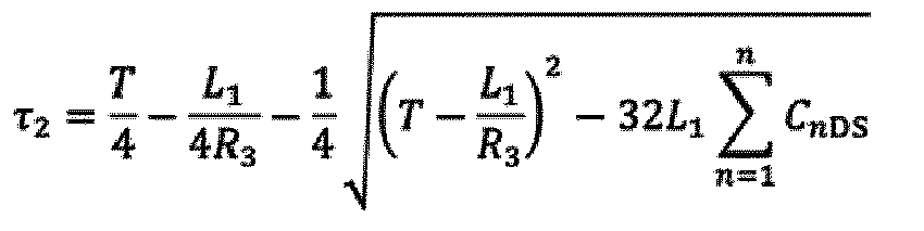
Applications Claiming Priority (2)
| Application Number | Priority Date | Filing Date | Title |
|---|---|---|---|
| JP2014225426A JP6359950B2 (en) | 2014-11-05 | 2014-11-05 | Transformer |
| PCT/JP2015/078736 WO2016072213A1 (en) | 2014-11-05 | 2015-10-09 | Transformer |
Publications (3)
| Publication Number | Publication Date |
|---|---|
| EP3217527A1 true EP3217527A1 (en) | 2017-09-13 |
| EP3217527A4 EP3217527A4 (en) | 2018-07-04 |
| EP3217527B1 EP3217527B1 (en) | 2019-11-20 |
Family
ID=55908940
Family Applications (1)
| Application Number | Title | Priority Date | Filing Date |
|---|---|---|---|
| EP15857728.8A Active EP3217527B1 (en) | 2014-11-05 | 2015-10-09 | Transformer |
Country Status (7)
| Country | Link |
|---|---|
| US (1) | US10122288B2 (en) |
| EP (1) | EP3217527B1 (en) |
| JP (1) | JP6359950B2 (en) |
| KR (1) | KR20170081165A (en) |
| CN (1) | CN107112908B (en) |
| TW (1) | TWI666866B (en) |
| WO (1) | WO2016072213A1 (en) |
Families Citing this family (1)
| Publication number | Priority date | Publication date | Assignee | Title |
|---|---|---|---|---|
| JPH089477B2 (en) | 1989-05-17 | 1996-01-31 | 日本レヂボン株式会社 | Handrail belt coating method |
Family Cites Families (33)
| Publication number | Priority date | Publication date | Assignee | Title |
|---|---|---|---|---|
| FR1064891A (en) | 1952-10-18 | 1954-05-18 | Csf | Improvements to impedance transformer networks |
| US4203151A (en) | 1978-09-21 | 1980-05-13 | Exxon Research & Engineering Co. | High-voltage converter circuit |
| US5570062A (en) | 1994-10-12 | 1996-10-29 | Ericsson Ge Mobile Communications Inc. | AM-FM transmitter power amplifier using class-BC |
| US5850337A (en) | 1997-07-25 | 1998-12-15 | Lucent Technologies Inc. | Magnetic-free DC/DC converter and method of operation thereof |
| US6462962B1 (en) * | 2000-09-08 | 2002-10-08 | Slobodan Cuk | Lossless switching DC-to-DC converter |
| JP3391773B2 (en) | 2000-09-14 | 2003-03-31 | 敏久 清水 | Immittance conversion circuit and converter using the same |
| FR2818463B1 (en) | 2000-12-18 | 2003-02-28 | Eisenmann France Sarl | HIGH VOLTAGE GENERATOR FOR ELECTROSTATIC PAINT EQUIPMENT |
| US7209370B2 (en) * | 2003-08-09 | 2007-04-24 | Astec International Limited | Circuit for reducing losses at light load in a soft switching full bridge converter |
| CN2798411Y (en) | 2004-12-02 | 2006-07-19 | 吴观晖 | DC convertor formed by electric field coupled transformer |
| EP2874297B1 (en) | 2006-06-06 | 2023-09-27 | Ideal Power Inc. | Buck-Boost power converter |
| DE102007030577A1 (en) | 2007-06-29 | 2009-01-02 | Sma Solar Technology Ag | Inverter for feeding electrical energy into a power supply network |
| EP2023475B1 (en) * | 2007-08-04 | 2016-10-12 | SMA Solar Technology AG | Inversion for a grounded DC source, in particular a photovoltaic generator |
| AT505801B1 (en) | 2007-09-20 | 2012-09-15 | Siemens Ag | METHOD FOR OPERATING AN ELECTRONICALLY CONTROLLED INVERTER |
| US8212541B2 (en) | 2008-05-08 | 2012-07-03 | Massachusetts Institute Of Technology | Power converter with capacitive energy transfer and fast dynamic response |
| JP5152511B2 (en) * | 2008-09-18 | 2013-02-27 | 住友電気工業株式会社 | Voltage conversion circuit |
| WO2010100737A1 (en) * | 2009-03-05 | 2010-09-10 | 東芝三菱電機産業システム株式会社 | Uninterruptible power supply device |
| CN102158096B (en) * | 2011-05-11 | 2013-11-20 | 南京博兰得电子科技有限公司 | Non-isolated resonant converter |
| DE202011102068U1 (en) * | 2011-06-07 | 2012-09-10 | Voltwerk Electronics Gmbh | Boost converter |
| BR112013033084A2 (en) * | 2011-07-01 | 2017-01-24 | Linak As | power supply with an output rectifier |
| JP5927826B2 (en) | 2011-09-28 | 2016-06-01 | 日産自動車株式会社 | Contactless power supply |
| US9248747B2 (en) * | 2011-11-29 | 2016-02-02 | Valeo Systemes De Controle Moteur | Converter for an electrical circuit designed to supply electrical propulsion power on board a motor vehicle |
| TWI488417B (en) * | 2011-11-29 | 2015-06-11 | Chung Ming Young | A non-isolated single-phase multilevel inverter for renewable energy system applications |
| US8829866B2 (en) | 2011-12-14 | 2014-09-09 | Volterra Semiconductor Corporation | DC to DC converter designed to mitigate problems associated with low duty cycle operation |
| JP5758866B2 (en) * | 2011-12-16 | 2015-08-05 | 旭化成エレクトロニクス株式会社 | Charge pump circuit and load drive system |
| CN102412728B (en) * | 2011-12-23 | 2014-09-17 | 航天长峰朝阳电源有限公司 | Chained large-power direct current converting circuit boosting voltages in positive direction |
| JP5598513B2 (en) * | 2012-08-29 | 2014-10-01 | 株式会社村田製作所 | Power system interconnection inverter device |
| JP5626293B2 (en) * | 2012-08-29 | 2014-11-19 | 株式会社村田製作所 | Inverter device |
| US8693224B1 (en) | 2012-11-26 | 2014-04-08 | Arctic Sand Technologies Inc. | Pump capacitor configuration for switched capacitor circuits |
| JP5878495B2 (en) * | 2013-06-11 | 2016-03-08 | 株式会社豊田中央研究所 | Electric vehicle power supply system |
| JP5695712B2 (en) | 2013-08-29 | 2015-04-08 | 住友電気工業株式会社 | Transformer |
| JP5727561B2 (en) * | 2013-08-29 | 2015-06-03 | 住友電気工業株式会社 | Transformer |
| JP5695782B1 (en) | 2013-09-12 | 2015-04-08 | 住友電気工業株式会社 | Transformer |
| CN105556821B (en) | 2013-09-19 | 2018-11-13 | 飞利浦照明控股有限公司 | The compact drive for being used in particular for light emitting diode with auxiliary output |
-
2014
- 2014-11-05 JP JP2014225426A patent/JP6359950B2/en active Active
-
2015
- 2015-10-09 WO PCT/JP2015/078736 patent/WO2016072213A1/en not_active Ceased
- 2015-10-09 KR KR1020177007914A patent/KR20170081165A/en not_active Withdrawn
- 2015-10-09 EP EP15857728.8A patent/EP3217527B1/en active Active
- 2015-10-09 CN CN201580054952.4A patent/CN107112908B/en not_active Expired - Fee Related
- 2015-10-09 US US15/509,296 patent/US10122288B2/en active Active
- 2015-10-29 TW TW104135621A patent/TWI666866B/en not_active IP Right Cessation
Also Published As
| Publication number | Publication date |
|---|---|
| EP3217527A4 (en) | 2018-07-04 |
| CN107112908B (en) | 2019-05-14 |
| JP2016092981A (en) | 2016-05-23 |
| US20170288559A1 (en) | 2017-10-05 |
| WO2016072213A1 (en) | 2016-05-12 |
| KR20170081165A (en) | 2017-07-11 |
| CN107112908A (en) | 2017-08-29 |
| EP3217527B1 (en) | 2019-11-20 |
| US10122288B2 (en) | 2018-11-06 |
| TW201624905A (en) | 2016-07-01 |
| JP6359950B2 (en) | 2018-07-18 |
| TWI666866B (en) | 2019-07-21 |
Similar Documents
| Publication | Publication Date | Title |
|---|---|---|
| US7449867B2 (en) | Multi-phase buck converter with a plurality of coupled inductors | |
| US10693387B2 (en) | Transformer | |
| Izadi et al. | A non‐isolated quadratic boost converter with improved gain, high efficiency, and continuous input current | |
| JP2008245516A (en) | Converters used for ion engines, etc. | |
| Li et al. | AC-DC converter with worldwide range input voltage by series and parallel piezoelectric transformer connection | |
| Ibanez et al. | Novel technique for bidirectional series‐resonant DC/DC converter in discontinuous mode | |
| CN104426382B (en) | Transformer | |
| EP3041123A1 (en) | Transformer | |
| EP3217528B1 (en) | Multi-stage voltage transformer | |
| EP3217527B1 (en) | Transformer | |
| US20130223109A1 (en) | Small size power supply | |
| JP7247247B2 (en) | power converter | |
| CN113809903B (en) | Method and apparatus for common mode voltage cancellation | |
| Fraytag et al. | Impact analysis of a multi‐variables modulation on the transformer of the dual‐active‐bridge converter | |
| KR102175583B1 (en) | Resonant converter including power network with passive devices | |
| KR100998064B1 (en) | DC-DC converters using leakage inductors for BCs as inductors for BCs | |
| Laugner et al. | Influence of the parasitic series inductance of the coupling capacitor of a SEPIC to the coil current waveforms with coupled inductors | |
| JP6144709B2 (en) | Transformer | |
| JP2017112679A (en) | Non-insulated composite resonant DC-DC converter |
Legal Events
| Date | Code | Title | Description |
|---|---|---|---|
| STAA | Information on the status of an ep patent application or granted ep patent |
Free format text: STATUS: THE INTERNATIONAL PUBLICATION HAS BEEN MADE |
|
| PUAI | Public reference made under article 153(3) epc to a published international application that has entered the european phase |
Free format text: ORIGINAL CODE: 0009012 |
|
| STAA | Information on the status of an ep patent application or granted ep patent |
Free format text: STATUS: REQUEST FOR EXAMINATION WAS MADE |
|
| 17P | Request for examination filed |
Effective date: 20170222 |
|
| AK | Designated contracting states |
Kind code of ref document: A1 Designated state(s): AL AT BE BG CH CY CZ DE DK EE ES FI FR GB GR HR HU IE IS IT LI LT LU LV MC MK MT NL NO PL PT RO RS SE SI SK SM TR |
|
| AX | Request for extension of the european patent |
Extension state: BA ME |
|
| DAV | Request for validation of the european patent (deleted) | ||
| DAX | Request for extension of the european patent (deleted) | ||
| A4 | Supplementary search report drawn up and despatched |
Effective date: 20180601 |
|
| RIC1 | Information provided on ipc code assigned before grant |
Ipc: H02M 3/155 20060101ALI20180525BHEP Ipc: H02M 3/158 20060101ALI20180525BHEP Ipc: H02M 5/22 20060101AFI20180525BHEP Ipc: H02M 5/293 20060101ALI20180525BHEP |
|
| GRAP | Despatch of communication of intention to grant a patent |
Free format text: ORIGINAL CODE: EPIDOSNIGR1 |
|
| STAA | Information on the status of an ep patent application or granted ep patent |
Free format text: STATUS: GRANT OF PATENT IS INTENDED |
|
| INTG | Intention to grant announced |
Effective date: 20190624 |
|
| RIN1 | Information on inventor provided before grant (corrected) |
Inventor name: YAMADA, KYOHEI Inventor name: NAKAHATA, HIDEAKI Inventor name: EGASHIRA, DAIYA Inventor name: HIROTSU, KENICHI Inventor name: OHIRA, TAKASHI |
|
| GRAS | Grant fee paid |
Free format text: ORIGINAL CODE: EPIDOSNIGR3 |
|
| GRAA | (expected) grant |
Free format text: ORIGINAL CODE: 0009210 |
|
| STAA | Information on the status of an ep patent application or granted ep patent |
Free format text: STATUS: THE PATENT HAS BEEN GRANTED |
|
| AK | Designated contracting states |
Kind code of ref document: B1 Designated state(s): AL AT BE BG CH CY CZ DE DK EE ES FI FR GB GR HR HU IE IS IT LI LT LU LV MC MK MT NL NO PL PT RO RS SE SI SK SM TR |
|
| REG | Reference to a national code |
Ref country code: GB Ref legal event code: FG4D |
|
| REG | Reference to a national code |
Ref country code: CH Ref legal event code: EP |
|
| REG | Reference to a national code |
Ref country code: IE Ref legal event code: FG4D |
|
| REG | Reference to a national code |
Ref country code: DE Ref legal event code: R096 Ref document number: 602015042288 Country of ref document: DE |
|
| REG | Reference to a national code |
Ref country code: AT Ref legal event code: REF Ref document number: 1205328 Country of ref document: AT Kind code of ref document: T Effective date: 20191215 |
|
| REG | Reference to a national code |
Ref country code: NL Ref legal event code: MP Effective date: 20191120 |
|
| REG | Reference to a national code |
Ref country code: LT Ref legal event code: MG4D |
|
| PG25 | Lapsed in a contracting state [announced via postgrant information from national office to epo] |
Ref country code: NL Free format text: LAPSE BECAUSE OF FAILURE TO SUBMIT A TRANSLATION OF THE DESCRIPTION OR TO PAY THE FEE WITHIN THE PRESCRIBED TIME-LIMIT Effective date: 20191120 Ref country code: LT Free format text: LAPSE BECAUSE OF FAILURE TO SUBMIT A TRANSLATION OF THE DESCRIPTION OR TO PAY THE FEE WITHIN THE PRESCRIBED TIME-LIMIT Effective date: 20191120 Ref country code: NO Free format text: LAPSE BECAUSE OF FAILURE TO SUBMIT A TRANSLATION OF THE DESCRIPTION OR TO PAY THE FEE WITHIN THE PRESCRIBED TIME-LIMIT Effective date: 20200220 Ref country code: GR Free format text: LAPSE BECAUSE OF FAILURE TO SUBMIT A TRANSLATION OF THE DESCRIPTION OR TO PAY THE FEE WITHIN THE PRESCRIBED TIME-LIMIT Effective date: 20200221 Ref country code: FI Free format text: LAPSE BECAUSE OF FAILURE TO SUBMIT A TRANSLATION OF THE DESCRIPTION OR TO PAY THE FEE WITHIN THE PRESCRIBED TIME-LIMIT Effective date: 20191120 Ref country code: BG Free format text: LAPSE BECAUSE OF FAILURE TO SUBMIT A TRANSLATION OF THE DESCRIPTION OR TO PAY THE FEE WITHIN THE PRESCRIBED TIME-LIMIT Effective date: 20200220 Ref country code: SE Free format text: LAPSE BECAUSE OF FAILURE TO SUBMIT A TRANSLATION OF THE DESCRIPTION OR TO PAY THE FEE WITHIN THE PRESCRIBED TIME-LIMIT Effective date: 20191120 Ref country code: LV Free format text: LAPSE BECAUSE OF FAILURE TO SUBMIT A TRANSLATION OF THE DESCRIPTION OR TO PAY THE FEE WITHIN THE PRESCRIBED TIME-LIMIT Effective date: 20191120 |
|
| PG25 | Lapsed in a contracting state [announced via postgrant information from national office to epo] |
Ref country code: RS Free format text: LAPSE BECAUSE OF FAILURE TO SUBMIT A TRANSLATION OF THE DESCRIPTION OR TO PAY THE FEE WITHIN THE PRESCRIBED TIME-LIMIT Effective date: 20191120 Ref country code: IS Free format text: LAPSE BECAUSE OF FAILURE TO SUBMIT A TRANSLATION OF THE DESCRIPTION OR TO PAY THE FEE WITHIN THE PRESCRIBED TIME-LIMIT Effective date: 20200320 Ref country code: HR Free format text: LAPSE BECAUSE OF FAILURE TO SUBMIT A TRANSLATION OF THE DESCRIPTION OR TO PAY THE FEE WITHIN THE PRESCRIBED TIME-LIMIT Effective date: 20191120 |
|
| PG25 | Lapsed in a contracting state [announced via postgrant information from national office to epo] |
Ref country code: AL Free format text: LAPSE BECAUSE OF FAILURE TO SUBMIT A TRANSLATION OF THE DESCRIPTION OR TO PAY THE FEE WITHIN THE PRESCRIBED TIME-LIMIT Effective date: 20191120 |
|
| PG25 | Lapsed in a contracting state [announced via postgrant information from national office to epo] |
Ref country code: ES Free format text: LAPSE BECAUSE OF FAILURE TO SUBMIT A TRANSLATION OF THE DESCRIPTION OR TO PAY THE FEE WITHIN THE PRESCRIBED TIME-LIMIT Effective date: 20191120 Ref country code: CZ Free format text: LAPSE BECAUSE OF FAILURE TO SUBMIT A TRANSLATION OF THE DESCRIPTION OR TO PAY THE FEE WITHIN THE PRESCRIBED TIME-LIMIT Effective date: 20191120 Ref country code: RO Free format text: LAPSE BECAUSE OF FAILURE TO SUBMIT A TRANSLATION OF THE DESCRIPTION OR TO PAY THE FEE WITHIN THE PRESCRIBED TIME-LIMIT Effective date: 20191120 Ref country code: DK Free format text: LAPSE BECAUSE OF FAILURE TO SUBMIT A TRANSLATION OF THE DESCRIPTION OR TO PAY THE FEE WITHIN THE PRESCRIBED TIME-LIMIT Effective date: 20191120 Ref country code: EE Free format text: LAPSE BECAUSE OF FAILURE TO SUBMIT A TRANSLATION OF THE DESCRIPTION OR TO PAY THE FEE WITHIN THE PRESCRIBED TIME-LIMIT Effective date: 20191120 Ref country code: PT Free format text: LAPSE BECAUSE OF FAILURE TO SUBMIT A TRANSLATION OF THE DESCRIPTION OR TO PAY THE FEE WITHIN THE PRESCRIBED TIME-LIMIT Effective date: 20200412 |
|
| REG | Reference to a national code |
Ref country code: AT Ref legal event code: MK05 Ref document number: 1205328 Country of ref document: AT Kind code of ref document: T Effective date: 20191120 |
|
| REG | Reference to a national code |
Ref country code: DE Ref legal event code: R097 Ref document number: 602015042288 Country of ref document: DE |
|
| PG25 | Lapsed in a contracting state [announced via postgrant information from national office to epo] |
Ref country code: SK Free format text: LAPSE BECAUSE OF FAILURE TO SUBMIT A TRANSLATION OF THE DESCRIPTION OR TO PAY THE FEE WITHIN THE PRESCRIBED TIME-LIMIT Effective date: 20191120 Ref country code: SM Free format text: LAPSE BECAUSE OF FAILURE TO SUBMIT A TRANSLATION OF THE DESCRIPTION OR TO PAY THE FEE WITHIN THE PRESCRIBED TIME-LIMIT Effective date: 20191120 |
|
| PLBE | No opposition filed within time limit |
Free format text: ORIGINAL CODE: 0009261 |
|
| STAA | Information on the status of an ep patent application or granted ep patent |
Free format text: STATUS: NO OPPOSITION FILED WITHIN TIME LIMIT |
|
| 26N | No opposition filed |
Effective date: 20200821 |
|
| PG25 | Lapsed in a contracting state [announced via postgrant information from national office to epo] |
Ref country code: PL Free format text: LAPSE BECAUSE OF FAILURE TO SUBMIT A TRANSLATION OF THE DESCRIPTION OR TO PAY THE FEE WITHIN THE PRESCRIBED TIME-LIMIT Effective date: 20191120 Ref country code: SI Free format text: LAPSE BECAUSE OF FAILURE TO SUBMIT A TRANSLATION OF THE DESCRIPTION OR TO PAY THE FEE WITHIN THE PRESCRIBED TIME-LIMIT Effective date: 20191120 Ref country code: AT Free format text: LAPSE BECAUSE OF FAILURE TO SUBMIT A TRANSLATION OF THE DESCRIPTION OR TO PAY THE FEE WITHIN THE PRESCRIBED TIME-LIMIT Effective date: 20191120 |
|
| PG25 | Lapsed in a contracting state [announced via postgrant information from national office to epo] |
Ref country code: IT Free format text: LAPSE BECAUSE OF FAILURE TO SUBMIT A TRANSLATION OF THE DESCRIPTION OR TO PAY THE FEE WITHIN THE PRESCRIBED TIME-LIMIT Effective date: 20191120 |
|
| REG | Reference to a national code |
Ref country code: CH Ref legal event code: PL |
|
| GBPC | Gb: european patent ceased through non-payment of renewal fee |
Effective date: 20201009 |
|
| PG25 | Lapsed in a contracting state [announced via postgrant information from national office to epo] |
Ref country code: MC Free format text: LAPSE BECAUSE OF FAILURE TO SUBMIT A TRANSLATION OF THE DESCRIPTION OR TO PAY THE FEE WITHIN THE PRESCRIBED TIME-LIMIT Effective date: 20191120 Ref country code: LU Free format text: LAPSE BECAUSE OF NON-PAYMENT OF DUE FEES Effective date: 20201009 |
|
| REG | Reference to a national code |
Ref country code: BE Ref legal event code: MM Effective date: 20201031 |
|
| PG25 | Lapsed in a contracting state [announced via postgrant information from national office to epo] |
Ref country code: LI Free format text: LAPSE BECAUSE OF NON-PAYMENT OF DUE FEES Effective date: 20201031 Ref country code: GB Free format text: LAPSE BECAUSE OF NON-PAYMENT OF DUE FEES Effective date: 20201009 Ref country code: BE Free format text: LAPSE BECAUSE OF NON-PAYMENT OF DUE FEES Effective date: 20201031 Ref country code: CH Free format text: LAPSE BECAUSE OF NON-PAYMENT OF DUE FEES Effective date: 20201031 |
|
| PG25 | Lapsed in a contracting state [announced via postgrant information from national office to epo] |
Ref country code: IE Free format text: LAPSE BECAUSE OF NON-PAYMENT OF DUE FEES Effective date: 20201009 |
|
| PG25 | Lapsed in a contracting state [announced via postgrant information from national office to epo] |
Ref country code: TR Free format text: LAPSE BECAUSE OF FAILURE TO SUBMIT A TRANSLATION OF THE DESCRIPTION OR TO PAY THE FEE WITHIN THE PRESCRIBED TIME-LIMIT Effective date: 20191120 Ref country code: MT Free format text: LAPSE BECAUSE OF FAILURE TO SUBMIT A TRANSLATION OF THE DESCRIPTION OR TO PAY THE FEE WITHIN THE PRESCRIBED TIME-LIMIT Effective date: 20191120 Ref country code: CY Free format text: LAPSE BECAUSE OF FAILURE TO SUBMIT A TRANSLATION OF THE DESCRIPTION OR TO PAY THE FEE WITHIN THE PRESCRIBED TIME-LIMIT Effective date: 20191120 |
|
| PG25 | Lapsed in a contracting state [announced via postgrant information from national office to epo] |
Ref country code: MK Free format text: LAPSE BECAUSE OF FAILURE TO SUBMIT A TRANSLATION OF THE DESCRIPTION OR TO PAY THE FEE WITHIN THE PRESCRIBED TIME-LIMIT Effective date: 20191120 |
|
| P01 | Opt-out of the competence of the unified patent court (upc) registered |
Effective date: 20230515 |
|
| PGFP | Annual fee paid to national office [announced via postgrant information from national office to epo] |
Ref country code: FR Payment date: 20230911 Year of fee payment: 9 |
|
| PGFP | Annual fee paid to national office [announced via postgrant information from national office to epo] |
Ref country code: DE Payment date: 20230830 Year of fee payment: 9 |
|
| REG | Reference to a national code |
Ref country code: DE Ref legal event code: R119 Ref document number: 602015042288 Country of ref document: DE |
|
| PG25 | Lapsed in a contracting state [announced via postgrant information from national office to epo] |
Ref country code: DE Free format text: LAPSE BECAUSE OF NON-PAYMENT OF DUE FEES Effective date: 20250501 |
|
| PG25 | Lapsed in a contracting state [announced via postgrant information from national office to epo] |
Ref country code: FR Free format text: LAPSE BECAUSE OF NON-PAYMENT OF DUE FEES Effective date: 20241031 |