EP3215834B1 - Wireless sensing devices and method for detecting hydration - Google Patents
Wireless sensing devices and method for detecting hydration Download PDFInfo
- Publication number
- EP3215834B1 EP3215834B1 EP15797508.7A EP15797508A EP3215834B1 EP 3215834 B1 EP3215834 B1 EP 3215834B1 EP 15797508 A EP15797508 A EP 15797508A EP 3215834 B1 EP3215834 B1 EP 3215834B1
- Authority
- EP
- European Patent Office
- Prior art keywords
- thermal
- sensor
- power
- sensing
- hydration
- Prior art date
- Legal status (The legal status is an assumption and is not a legal conclusion. Google has not performed a legal analysis and makes no representation as to the accuracy of the status listed.)
- Active
Links
- 230000036571 hydration Effects 0.000 title claims description 47
- 238000006703 hydration reaction Methods 0.000 title claims description 47
- 238000000034 method Methods 0.000 title claims description 16
- 239000000758 substrate Substances 0.000 claims description 53
- 238000003306 harvesting Methods 0.000 claims description 45
- 230000004907 flux Effects 0.000 claims description 13
- 238000001816 cooling Methods 0.000 claims description 8
- 239000011343 solid material Substances 0.000 claims description 5
- 239000011344 liquid material Substances 0.000 claims description 3
- 230000003213 activating effect Effects 0.000 claims description 2
- 230000005284 excitation Effects 0.000 description 54
- 238000010438 heat treatment Methods 0.000 description 41
- 239000000463 material Substances 0.000 description 37
- 230000008878 coupling Effects 0.000 description 19
- 238000010168 coupling process Methods 0.000 description 19
- 238000005859 coupling reaction Methods 0.000 description 19
- 239000007788 liquid Substances 0.000 description 17
- 230000008859 change Effects 0.000 description 16
- 230000003287 optical effect Effects 0.000 description 16
- 238000004146 energy storage Methods 0.000 description 15
- 230000000704 physical effect Effects 0.000 description 15
- 238000005259 measurement Methods 0.000 description 14
- 238000010521 absorption reaction Methods 0.000 description 13
- 239000002131 composite material Substances 0.000 description 12
- 239000010410 layer Substances 0.000 description 11
- 238000004891 communication Methods 0.000 description 10
- 239000007787 solid Substances 0.000 description 10
- 238000010586 diagram Methods 0.000 description 9
- 230000005855 radiation Effects 0.000 description 9
- 230000004044 response Effects 0.000 description 9
- 238000012546 transfer Methods 0.000 description 9
- 239000007789 gas Substances 0.000 description 8
- 230000004913 activation Effects 0.000 description 7
- 230000001105 regulatory effect Effects 0.000 description 7
- 238000012545 processing Methods 0.000 description 6
- 230000001276 controlling effect Effects 0.000 description 5
- 239000012530 fluid Substances 0.000 description 5
- 230000001419 dependent effect Effects 0.000 description 4
- 239000000203 mixture Substances 0.000 description 4
- 230000002093 peripheral effect Effects 0.000 description 4
- 230000006903 response to temperature Effects 0.000 description 4
- XLYOFNOQVPJJNP-UHFFFAOYSA-N water Substances O XLYOFNOQVPJJNP-UHFFFAOYSA-N 0.000 description 4
- 239000000443 aerosol Substances 0.000 description 3
- 238000004458 analytical method Methods 0.000 description 3
- 239000003990 capacitor Substances 0.000 description 3
- 238000013500 data storage Methods 0.000 description 3
- 230000005672 electromagnetic field Effects 0.000 description 3
- 239000000945 filler Substances 0.000 description 3
- 239000006260 foam Substances 0.000 description 3
- 230000006870 function Effects 0.000 description 3
- 230000003071 parasitic effect Effects 0.000 description 3
- 229920006254 polymer film Polymers 0.000 description 3
- 230000001052 transient effect Effects 0.000 description 3
- 241000124008 Mammalia Species 0.000 description 2
- 230000005678 Seebeck effect Effects 0.000 description 2
- 239000012790 adhesive layer Substances 0.000 description 2
- 238000013459 approach Methods 0.000 description 2
- 230000009286 beneficial effect Effects 0.000 description 2
- 230000008901 benefit Effects 0.000 description 2
- 239000002612 dispersion medium Substances 0.000 description 2
- 238000009826 distribution Methods 0.000 description 2
- 238000005516 engineering process Methods 0.000 description 2
- 230000007613 environmental effect Effects 0.000 description 2
- 239000012212 insulator Substances 0.000 description 2
- 239000011159 matrix material Substances 0.000 description 2
- 239000002609 medium Substances 0.000 description 2
- 238000012986 modification Methods 0.000 description 2
- 230000004048 modification Effects 0.000 description 2
- 239000002245 particle Substances 0.000 description 2
- 239000002861 polymer material Substances 0.000 description 2
- 239000004814 polyurethane Substances 0.000 description 2
- 229920002635 polyurethane Polymers 0.000 description 2
- 230000008569 process Effects 0.000 description 2
- 239000004065 semiconductor Substances 0.000 description 2
- 229920000247 superabsorbent polymer Polymers 0.000 description 2
- NIXOWILDQLNWCW-UHFFFAOYSA-M Acrylate Chemical compound [O-]C(=O)C=C NIXOWILDQLNWCW-UHFFFAOYSA-M 0.000 description 1
- 229910052582 BN Inorganic materials 0.000 description 1
- PZNSFCLAULLKQX-UHFFFAOYSA-N Boron nitride Chemical compound N#B PZNSFCLAULLKQX-UHFFFAOYSA-N 0.000 description 1
- 230000005679 Peltier effect Effects 0.000 description 1
- 229920002614 Polyether block amide Polymers 0.000 description 1
- 239000004372 Polyvinyl alcohol Substances 0.000 description 1
- 239000000853 adhesive Substances 0.000 description 1
- 230000001070 adhesive effect Effects 0.000 description 1
- 239000002390 adhesive tape Substances 0.000 description 1
- 229910052782 aluminium Inorganic materials 0.000 description 1
- XAGFODPZIPBFFR-UHFFFAOYSA-N aluminium Chemical compound [Al] XAGFODPZIPBFFR-UHFFFAOYSA-N 0.000 description 1
- 230000002457 bidirectional effect Effects 0.000 description 1
- 230000033228 biological regulation Effects 0.000 description 1
- 230000005540 biological transmission Effects 0.000 description 1
- 238000009529 body temperature measurement Methods 0.000 description 1
- 239000013590 bulk material Substances 0.000 description 1
- 239000001913 cellulose Substances 0.000 description 1
- 229920002678 cellulose Polymers 0.000 description 1
- 239000000919 ceramic Substances 0.000 description 1
- 239000000084 colloidal system Substances 0.000 description 1
- 239000004020 conductor Substances 0.000 description 1
- 238000010276 construction Methods 0.000 description 1
- 238000013461 design Methods 0.000 description 1
- 238000011161 development Methods 0.000 description 1
- 230000005670 electromagnetic radiation Effects 0.000 description 1
- 239000000839 emulsion Substances 0.000 description 1
- 238000002474 experimental method Methods 0.000 description 1
- 210000000416 exudates and transudate Anatomy 0.000 description 1
- 230000005669 field effect Effects 0.000 description 1
- 238000001914 filtration Methods 0.000 description 1
- 239000008241 heterogeneous mixture Substances 0.000 description 1
- 230000006698 induction Effects 0.000 description 1
- 238000009413 insulation Methods 0.000 description 1
- 230000003993 interaction Effects 0.000 description 1
- 150000002632 lipids Chemical class 0.000 description 1
- 230000007774 longterm Effects 0.000 description 1
- 239000000696 magnetic material Substances 0.000 description 1
- 238000004519 manufacturing process Methods 0.000 description 1
- 238000013507 mapping Methods 0.000 description 1
- 229910052751 metal Inorganic materials 0.000 description 1
- 239000002184 metal Substances 0.000 description 1
- 239000007769 metal material Substances 0.000 description 1
- 150000002739 metals Chemical class 0.000 description 1
- TWNQGVIAIRXVLR-UHFFFAOYSA-N oxo(oxoalumanyloxy)alumane Chemical compound O=[Al]O[Al]=O TWNQGVIAIRXVLR-UHFFFAOYSA-N 0.000 description 1
- 229920002401 polyacrylamide Polymers 0.000 description 1
- 229920000058 polyacrylate Polymers 0.000 description 1
- 229920000728 polyester Polymers 0.000 description 1
- 229920006149 polyester-amide block copolymer Polymers 0.000 description 1
- 229920000642 polymer Polymers 0.000 description 1
- 229920002451 polyvinyl alcohol Polymers 0.000 description 1
- 239000011148 porous material Substances 0.000 description 1
- 230000031070 response to heat Effects 0.000 description 1
- 238000000926 separation method Methods 0.000 description 1
- 238000005549 size reduction Methods 0.000 description 1
- 230000008326 skin blood flow Effects 0.000 description 1
- 230000037067 skin hydration Effects 0.000 description 1
- 230000005236 sound signal Effects 0.000 description 1
- 230000007480 spreading Effects 0.000 description 1
- 238000003892 spreading Methods 0.000 description 1
- 230000003068 static effect Effects 0.000 description 1
- 238000003860 storage Methods 0.000 description 1
- 239000004583 superabsorbent polymers (SAPs) Substances 0.000 description 1
- 239000000725 suspension Substances 0.000 description 1
- 210000004243 sweat Anatomy 0.000 description 1
- 230000028016 temperature homeostasis Effects 0.000 description 1
- 230000002123 temporal effect Effects 0.000 description 1
- 230000026683 transduction Effects 0.000 description 1
- 238000010361 transduction Methods 0.000 description 1
Images


Classifications
-
- G—PHYSICS
- G01—MEASURING; TESTING
- G01N—INVESTIGATING OR ANALYSING MATERIALS BY DETERMINING THEIR CHEMICAL OR PHYSICAL PROPERTIES
- G01N25/00—Investigating or analyzing materials by the use of thermal means
- G01N25/56—Investigating or analyzing materials by the use of thermal means by investigating moisture content
-
- A—HUMAN NECESSITIES
- A61—MEDICAL OR VETERINARY SCIENCE; HYGIENE
- A61B—DIAGNOSIS; SURGERY; IDENTIFICATION
- A61B5/00—Measuring for diagnostic purposes; Identification of persons
- A61B5/0002—Remote monitoring of patients using telemetry, e.g. transmission of vital signals via a communication network
- A61B5/0004—Remote monitoring of patients using telemetry, e.g. transmission of vital signals via a communication network characterised by the type of physiological signal transmitted
- A61B5/0008—Temperature signals
-
- A—HUMAN NECESSITIES
- A61—MEDICAL OR VETERINARY SCIENCE; HYGIENE
- A61B—DIAGNOSIS; SURGERY; IDENTIFICATION
- A61B5/00—Measuring for diagnostic purposes; Identification of persons
- A61B5/44—Detecting, measuring or recording for evaluating the integumentary system, e.g. skin, hair or nails
- A61B5/441—Skin evaluation, e.g. for skin disorder diagnosis
- A61B5/443—Evaluating skin constituents, e.g. elastin, melanin, water
-
- G—PHYSICS
- G01—MEASURING; TESTING
- G01F—MEASURING VOLUME, VOLUME FLOW, MASS FLOW OR LIQUID LEVEL; METERING BY VOLUME
- G01F23/00—Indicating or measuring liquid level or level of fluent solid material, e.g. indicating in terms of volume or indicating by means of an alarm
- G01F23/22—Indicating or measuring liquid level or level of fluent solid material, e.g. indicating in terms of volume or indicating by means of an alarm by measuring physical variables, other than linear dimensions, pressure or weight, dependent on the level to be measured, e.g. by difference of heat transfer of steam or water
-
- G—PHYSICS
- G01—MEASURING; TESTING
- G01N—INVESTIGATING OR ANALYSING MATERIALS BY DETERMINING THEIR CHEMICAL OR PHYSICAL PROPERTIES
- G01N27/00—Investigating or analysing materials by the use of electric, electrochemical, or magnetic means
- G01N27/02—Investigating or analysing materials by the use of electric, electrochemical, or magnetic means by investigating impedance
- G01N27/04—Investigating or analysing materials by the use of electric, electrochemical, or magnetic means by investigating impedance by investigating resistance
- G01N27/14—Investigating or analysing materials by the use of electric, electrochemical, or magnetic means by investigating impedance by investigating resistance of an electrically-heated body in dependence upon change of temperature
- G01N27/18—Investigating or analysing materials by the use of electric, electrochemical, or magnetic means by investigating impedance by investigating resistance of an electrically-heated body in dependence upon change of temperature caused by changes in the thermal conductivity of a surrounding material to be tested
-
- H—ELECTRICITY
- H02—GENERATION; CONVERSION OR DISTRIBUTION OF ELECTRIC POWER
- H02J—CIRCUIT ARRANGEMENTS OR SYSTEMS FOR SUPPLYING OR DISTRIBUTING ELECTRIC POWER; SYSTEMS FOR STORING ELECTRIC ENERGY
- H02J50/00—Circuit arrangements or systems for wireless supply or distribution of electric power
- H02J50/20—Circuit arrangements or systems for wireless supply or distribution of electric power using microwaves or radio frequency waves
-
- A—HUMAN NECESSITIES
- A61—MEDICAL OR VETERINARY SCIENCE; HYGIENE
- A61B—DIAGNOSIS; SURGERY; IDENTIFICATION
- A61B2560/00—Constructional details of operational features of apparatus; Accessories for medical measuring apparatus
- A61B2560/02—Operational features
- A61B2560/0204—Operational features of power management
- A61B2560/0214—Operational features of power management of power generation or supply
Definitions
- the present disclosure relates to wireless sensing devices and systems. At least part of the present disclosure relates to wireless sensing devices having excitation components. At least part of the present disclosure relates to wearable wireless sensors for measuring one or more thermal properties.
- an RF hydration sensor comprises a substrate; an antenna disposed on the substrate; an RF circuit electrically coupled to the antenna, the RF circuit comprising a processor; a thermal source electrically coupled to the RF circuit for changing a thermal condition of a target area; and a sensing element thermally coupled to the thermal source for sensing a temperature of the thermal source, the RF hydration sensor being configured such that when the thermal source is thermally coupled to the target area, the RF hydration sensor wirelessly receives a first power having a first form from a transceiver, the RF circuit transforms the first power to a second power having a second form different from the first form and delivers the second power to the thermal source, the sensing element senses a time variation of the thermal source temperature, and the processor determines a hydration indicator indicating hydration level based on the sensed time variation of the thermal source temperature.
- a method of determining hydration level using the RF hydration sensor comprises the step of: disposing the thermal source proximate to an object; wirelessly activating the thermal source; generating a series of sensing signals by the sensing element; determining, by the processor, a thermal property of the object based on at least some of the series of sensing signals; and generating, by the processor, a hydration indicator indicative of hydration level of the object based on the determined thermal property and a reference data.
- spatially related terms including but not limited to, “lower,” “upper,” “beneath,” “below,” “above,” and “on top,” if used herein, are utilized for ease of description to describe spatial relationships of an element(s) to another.
- Such spatially related terms encompass different orientations of the device in use or operation in addition to the particular orientations depicted in the figures and described herein. For example, if an object depicted in the figures is turned over or flipped over, portions previously described as below or beneath other elements would then be above those other elements.
- an element, component or layer for example when an element, component or layer for example is described as forming a "coincident interface" with, or being “on” “connected to,” “coupled with” or “in contact with” another element, component or layer, it can be directly on, directly connected to, directly coupled with, in direct contact with, or intervening elements, components or layers may be on, connected, coupled or in contact with the particular element, component or layer, for example.
- an element, component or layer for example is referred to as being “directly on,” “directly connected to,” “directly coupled with,” or “directly in contact with” another element, there are no intervening elements, components or layers for example.
- electrostatic coupled and “electrically coupled” are used interchangeably.
- layers, components, or elements may be described as being adjacent one another. Layers, components, or elements can be adjacent one another by being in direct contact, by being connected through one or more other components, or by being held next to one another or attached to one another. Layers, components, or elements that are in direct contact may be described as being immediately adjacent.
- RF radio frequency
- NFC near field communication
- Sensors based on RF technology enable beneficial system attributes, such as wireless readout, passive (battery-free) sensor operation, unique sensor identification, compatibility with the human body, and onboard micro-processing capabilities.
- beneficial system attributes such as wireless readout, passive (battery-free) sensor operation, unique sensor identification, compatibility with the human body, and onboard micro-processing capabilities.
- NFC includes but is not limited to the set of standard protocols defined by the NFC Forum industry association.
- At least some aspects of the present disclosure feature wireless sensing devices for measuring thermal properties that can transmit sensor signals via a wireless interface.
- a wireless interface includes far field communications and NFC.
- the wireless sensing device use NFC as communication interface.
- the wireless sensing device includes an energy harvesting device to receive and convert power and supply power to at least some of the other components of the wireless sensing devices.
- a wireless sensing device has a single antenna with two or more sensors and excitation devices, where each sensor is coupled to an RF device having a unique identifier and each sensor is coupled to an excitation device.
- the wireless sensing device can provide sensor signals from the spatially dispersed sensors to a computing device to determine physical properties based on spatial information and sensor signals.
- a wireless sensing device has thermally isolated regions, where each region includes a thermal sensor and optional thermal source, the measurement of the thermal sensors can be used to determine thermal properties of an object of interest.
- the wireless sensing device has one thermal region A comprising materials with high thermal conductivity and a region B that is thermally isolated from the region A, where the region A is in thermal contact with an object of interest.
- the thermal property of the object can be determined based on differential sensor signals from sensor A disposed proximate to region A and sensor B disposed proximate to region B.
- the wireless sensing system includes multiple sensors that are spatially separated and receives sensing signals from these sensors.
- the wireless sensing system can establish an array or a map of sensing signals and thereby evaluate physical properties of a material or object at various parts corresponding to sensor positions.
- the wireless sensing system receives sensing signals that are temporally separated, from a wireless sensing device to measure a physical property of an object.
- the wireless sensing system can establish a profile of sensing signal changes over time and thereby determine physical property of the object based on the profile. For example, the wireless sensing system can establish a temperature-time profile with one or more thermal sensors and determine water content within the material or object and further evaluate a hydration or moisture level of the material or object.
- Thermal properties of a material or an object include, for example, thermal conductivity, thermal conductance, specific heat capacity, heat capacity, thermal diffusivity, or the like.
- Thermal conductivity is intrinsic temperature difference in response to an applied heat flux through a material, with typical units of power per length-temperature, such as watts per meter-Kelvin.
- Thermal conductance takes into account cross-sectional area of heat flux and material thickness, with typical units of power per temperature, such as watts per Kelvin.
- Specific heat capacity is intrinsic temperature rise in response to heat energy, with typical units of energy per mass-temperature, such as joules per kilogram-Kelvin.
- Heat capacity takes into account mass of material, with typical units of energy per temperature, such as joules per Kelvin.
- Thermal diffusivity is the ratio of thermal conductivity to the product of mass density and specific heat capacity and indicates how quickly a material would reach a temperature similar to its surrounding environment, with typical units of area per time, such as square meters per second.
- a material or an object can be a composite, where thermal properties of a composite refer to effective or average thermal properties for the composite.
- Some composites have a dispersed phase in a dispersion medium, which are generally known as solutions, as colloids, or as suspensions depending on the length scale involved.
- the composite can be one-phase or mixed-phase, containing one or more of solids, liquids, or gases.
- thermal properties of composites whose dispersion medium is not a gas are measured and/or calculated.
- the non-aerosol composites include, for example, foams (i.e., gas dispersed in solid or liquid), emulsions (i.e., liquid dispersed in liquid or in solid), or sols (i.e., solid dispersed in liquid or in solid).
- the non-aerosol composites may also include, for example, a heterogeneous mixture of solids, liquids, or gases that are dispersed in a solid or liquid matrix.
- the effective thermal conductivity of an acrylate adhesive having dispersed particles of aluminum oxide is based on the thermal conductivity of each material, the mixing fraction, and other properties such as particle shape.
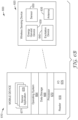
- FIG. 1A illustrates a block diagram of one embodiment of a wireless sensing device 100A, which can be used to measure a thermal property of an object.
- a wireless sensing device is typically in an assembly.
- the wireless sensing device 100A includes a substrate 110, a control circuit 120 disposed on the substrate 110, a transceiver 130 electronically coupled to the control circuit, an antenna 135 electronically coupled to the transceiver and disposed on the substrate 110, an energy harvesting device 140 disposed on the substrate, an optional thermal source 150 and a sensor 160.
- the energy harvesting device 140 is electronically coupled to the antenna 135.
- the antenna 135 is configured to transmit signals when an RF reader interrogates the wireless sensing device 100A, for example.
- the wireless sensing device 100A has an optional thermal spreader 115, which includes solid, liquid, or composite material and has a desired or known thermal property.
- the thermal conductivity of the thermal spreader 115 is higher than the thermal conductivity of the substrate 110.
- the substrate is the thermal spreader that is configured to be in thermal contact with the object when the wireless sensing device is in use for measuring the thermal property of the object.
- the thermal spreader 115 includes a polymer film or an adhesive layer.
- the thermal spreader 115 has a thermal conductivity greater than or equal to 0.1 watts per meter-Kelvin.
- the thermal spreader 115 may include metallic fillers, such as aluminum, or ceramic fillers, such as boron nitride. In some cases, fillers used in the thermal spreader are to obtain a desired thermal conductivity. In some embodiments, the wireless sensing device 100A may improve accuracy of measurement results by providing generally uniform thermal flux through the thermal spreader 115. In some cases, the wireless sensing device 100A may use the thermal property of the thermal spreader 115 in determining the thermal property of the object.
- Thermal flux or heat flux is the transfer of thermal energy through a medium by conduction (phonons), convection (fluid flow), or radiation (photons).
- the thermal flux of primary interest is that the thermal flux moves to and from a thermal source by conduction, and where the thermal flux is spread to or from a surface of a region or substrate.
- the substrate 110 can be flexible or rigid. In some embodiments, the substrate 110 is stretchable. In some embodiments, the substrate 110 includes polyurethane. In some embodiments, the substrate 110 is a polymeric film. Suitable polymer films include elastomeric polyurethane, co-polyester, or polyether block amide films.
- the control circuit 120 can include one or more electronic components that are electronically connected.
- the control circuit 120 can include passive electronic components, for example, such as resistors, capacitors, inductors, transformers, diodes, and the like.
- the control circuit 120 can include active electronic components such as transistors, voltage or current sources, amplifiers, microprocessors, oscillators, analog-to-digital converters, digital-to-analog converters, phase-locked loops, and the like. In some cases, the control circuit 120 may be formed into an integrated circuit or include an integrated circuit.
- a microprocessor may be a state machine with relatively simple digital logic to move among two or more states in a pre-defined manner, or a microcontroller comprised of an instruction set, digital processing blocks, memory, firmware, and peripherals such as clocks, memory controllers, and data converters.
- the control circuit 120 comprises a microprocessor and a memory storing a unique identifier.
- the control circuit 120, the transceiver 130, and the antenna 135 are components of a radio frequency identification (RFID) tag.
- RFID radio frequency identification
- RFID tags on flexible and/or stretchable substrates are described in more details in U.S. Patent Application No. 62/031,581, entitled “RFID Tag on Stretchable Substrate” and filed on July 31, 2014 , and U.S. Patent Application No. 62/031,603, entitled “RFID Tag on Flexible Substrate” and filed on July 31, 2014 .
- the thermal source 150 is disposed proximate the thermal spreader 115 to generate thermal flux in the thermal spreader 115.
- the thermal source 150 is electronically coupled to the energy harvesting device 140 and generates thermal flux in the thermal spreader 115.
- the sensor 160 is disposed in the thermal spreader 115 and electronically coupled to the control circuit 120.
- the sensor 160 is configured to generate a sensor signal indicating a temperature and provide the sensor signal to the control circuit 120.
- the thermal source 150 and the sensor 160 are components of an integrated circuit. In some implementations, the thermal source 150 and the sensor 160 are a same resistive element.
- the thermal source 150 may generate heat by Joule heating, for example, by passing current through any electrical component that has a non-zero electrical resistance.
- the thermal source 150 can be a resistor electronically connected to a source of current, or indirectly such as a metallic or magnetic material coupled to a changing magnetic field to produce electrical current by magnetic induction.
- the thermal source 150 can be a thermoelectric device operating based on the Peltier effect, such as a thermoelectric heater or cooler containing one or more junctions of p-type and n-type thermoelectric materials, typically wired electronically in series. Depending on the polarity of the electrical current, one portion of the thermoelectric device will increase in temperature and another portion will decrease in temperature, so the thermoelectric device may be used for heating and/or cooling. Such thermoelectric thermal sources may also have thermal contributions from Joule heating due to the non-zero electrical resistance of the elements.
- the thermal source 150 can be based on optical absorption, from an intentional source or from an ambient source of optical energy. In some other cases, the thermal source can include a parasitic element or otherwise unintentional source of heating or cooling. In some cases, the thermal source 150 is a dedicated component in the wireless sensing device 100A. In some other cases, the thermal source 150 includes one or more electronic components that are in operation in the wireless sensing device. For example, the thermal source 150 may include a transceiver element that generates additional heating during operation. As another example, the thermal source 150 includes a microprocessor element that generates heat during operation.
- the thermal source 150 is disposed proximate to the thermal spreader 115.
- the thermal spreader 115 has a known thermal property, which can be used to determine one or more thermal properties of the object.
- the thermal source includes a high conductivity component.
- the thermal source 150 and/or thermal spreader 115 is in thermal contact with the object or material of interest. Thermal contact is defined at an interface of two materials, where non-infinite thermal contact conductance results in a temperature difference across the interface when heat flux moves across the interface.
- the interface generally consists of a mixed-phase region similar to some of the composite materials described.
- the interface may comprise solid regions with some roughness or within the solid regions, where fluid regions within that roughness.
- Fluid regions can include liquid, gas, or a mixture.
- the interface may have solid or liquid regions with gas regions in one or more voids or at a surface. Maintaining good thermal contact or thermal coupling typically involves limiting the fraction of fluid regions especially those containing gas.
- Thermal interface materials are typically used for this purpose, such as elastomeric pads, adhesive tapes, greases, or the like.
- Effective contact thermal conductance is the inverse of temperature difference across a contact interface area for a given heat flux, having typical units of watts per square meter per Kelvin. Effective contact thermal conductance may be additionally scaled by an effective thickness of the contact region to obtain an effective contact thermal conductivity, having typical units of watts per meter per Kelvin.
- the sensor 160 also referred to as sensing element, may be a thermal sensor that has measurable changes in electrical property, optical property, acoustic property, or the like, in response to temperature changes.
- electrical thermal sensors can have a response to temperature changes in electrical voltage, current, or resistance.
- a resistive thermal sensor has its electrical resistance dependent on temperature; typical metals are resistive thermal devices where resistance increases with temperature in a relatively linear relationship.
- a thermistor typically has a resistance that depends on electrical current and non-linear resistance changes in response to temperature changes.
- electrical thermal sensors may operate based on the Seebeck effect to convert a temperature difference into an electrical voltage, such as a thermocouple or thermopile.
- An optical temperature sensor includes an optical transducer that receives electromagnetic radiation from objects out of thermal equilibrium with their environment, where the transducer temperature changes as it absorbs and emits radiation, for example, bolometers, microbolometers, pyroelectric detectors, or the like. These sensors combine optical and electrical aspects, where incident and reflected radiation is measured and converted to an electrical response when the transducer is heated or cooled by the radiation.
- An acoustic temperature sensor relies on the temperature-induced change in propagation of mechanical waves through a bulk material or along the surface of a material.
- a sensor to measure temperature can comprise multilayer structures that deform in response to temperature based on differing thermal expansion properties of the layers. The deformation can be transduced electronically, such as a deformed beam that completes an electromechanical switch, or transduced as a visible indicator by means of a dial or other element.
- the energy harvesting device 140 comprises a bridge rectifier, a rectifier, a diode or transistor rectifier, and may include a voltage or current regulator.
- non-rectified electrical power may be provided to the thermal source (e.g., resistor), while the remainder of the electronic circuitry typically operates on rectified power.
- An energy harvesting device according to the invention receives power from an intentional radiation source or from an unintentional or ambient source. Intentional radiation sources may include, for example, an RF reader.
- an RF reader can produce a near-field electrical or magnetic field that stores energy for coupling into one or more target devices, or it can produce a far-field radiation pattern of traveling electromagnetic waves, or a combination thereof.
- the magnetic field may couple to the antenna 135 and the energy harvesting device 140 to induce an electrical current in the wireless sensing device from the magnetic field.
- the energy harvesting device 140 is configured to be coupled to an unintentional or ambient source, for example, such as an optical source, inertial vibration source, or temperature gradient source, or the like.
- An optical source can be, for example sunlight, artificial lighting, or the like.
- the energy harvesting device 140 can include photovoltaic cells to convert optical energy to electrical energy.
- An inertial or vibration source of energy can be, for example, a motor, a moving transportation vehicle (e.g., automobile, train, airplane, etc.), wind, or the like. It can also be a biological source such as a human in motion.
- the energy harvesting device can include a piezoelectric device that converts mechanical energy to electrical energy.
- the energy harvesting device 140 can obtain electrical energy from a temperature gradient.
- the energy harvesting device can include a thermoelectric device operating based on Seebeck effect that converts the temperature gradient and heat flow resulting from the skin of a mammal or from the outside of a pipe containing a process fluid into electrical energy.
- the thermal source 150 is regulated.
- the thermal source 150 can be regulated by the processing components of the control circuit 120, by interaction with an external device through the transceiver 130, the energy harvesting device 140, or by a combination thereof.
- the control circuit 120 regulates the thermal source 150.
- the control circuit 120 regulates the thermal source 150 based on sensor signals.
- the power delivered to the thermal source 150 can be modulated by a controller within the control circuit 120, for example, by changing the amount of electrical power delivered to the thermal source 150.
- the control circuit 120 regulates the electrical power in order to maintain constant temperature or maintain a desired rate of change in temperature in response to the sensing signal indicative of temperature provided by the sensor 160, which is a closed-loop control based on temperature.
- the control circuit 120 regulates the electrical power into the thermal source in order to maintain constant power or a desired rate of change in power supplied to the thermal source 150, which is a closed-loop control based on power.
- the thermal source 150 receives a known but uncontrolled current, voltage, or power, and the known value is used in later computation step(s) to account for variation in power which is an open-loop control.
- an open-loop type of control may be implemented with contingent constraints, such as a maximum or minimum value of a sensing signal obtained from sensor 160 and used by the control circuit 120 to adjust the thermal source 150 if the sensing signal is outside the maximum or minimum value.
- the thermal source 150 can be regulated by performing the measurement during a time period when a dominant parasitic/unintended heating element is operating. Such regulation can be done directly through an intentional increase in the operating load of the parasitic/unintended heating element.
- the controller can instruct a transceiver to turn on and process otherwise nonsensical data in order to generate additional heat.
- the power supplied to the transceiver can be monitored by the controller, with the processing load adjusted to maintain a constant power or desired rate of change in power.
- the wireless sensing device 100A may include an optional energy storage device 170 that is disposed on the substrate and electronically coupled to the energy harvesting device 140.
- Energy storage devices 170 may include capacitors or supercapacitors.
- the energy storage device 170 may store energy harvested from the energy harvesting device 140 for a short or long term period of time. Energy stored in the energy storage device 170 may be used to provide power to designated components of the wireless sensing device 100A including, but not limited to, the control circuit 120, thermal source 150, and sensor 160.
- the wireless sensing device 100A can continue to operate on power stored in the energy storage device 170.
- energy stored in the energy storage device 170 can be used to augment the power available from the energy harvesting device 140, enabling higher power availability than the power available from the energy storage device 170 or the energy harvesting device 140 alone.
- the energy harvesting device 140 provides power to the thermal source 150, and possibly other components of the wireless sensing device 100A, such as the sensor 160, the control circuit 120, and the transceiver 130.
- the sensor 160 is configured to generate a first sensor signal before the thermal source 150 is activated by the energy harvesting device 140 and a second sensor signal after the thermal source 150 is activated by the energy harvesting device 140.
- the control circuit can determine a thermal property of the object based on the first and second sensor signals.
- the sensor 160 is configured to generate a first sensor signal approximately concurrent with the activation of the thermal source 150 by the energy harvesting device 140, and a second sensor signal after the thermal source 150 is activated by the energy harvesting device 140.
- the transceiver 130 can include a transmitter element and/or a receiver element.
- a transmitter element includes one or more electromagnetic or electroacoustic transducers, and electronic components to filter, amplify, and modulate one or more signals.
- a receiver element comprises one or more electromagnetic or electroacoustic transducers that can be shared with those of the transmitter element via a switching means or can be separate from those of the transmitter element, and electronics to filter, amplify and demodulate one or more signals from the received energy.
- An electromagnetic transducer can be an antenna, which can be designed to radiate electromagnetic fields from input electrical signals and absorb electromagnetic fields into electrical signals, or can be designed to couple with stored energy in electromagnetic near fields, or a combination of both radiation and near-field coupling.
- An electromagnetic transducer can also be a light-emitting diode or other optical source, or a photodiode or other optical detector.
- An electroacoustic transducer can be a loudspeaker or other acoustic source, or a microphone or other acoustic detector. Electromagnetic and/or electroacoustic transducers can be combined into a single element that is capable of bidirectional transduction from electrical signals to electromagnetic or acoustic energy, and from electromagnetic or acoustic energy to electrical signals.
- the transceiver 130 can be included in an integrated circuit device, for example, NTAG213 from NXP Semiconductors (Eindhoven, the Netherlands).
- the transceiver 130 can be an infrared transceiver element with a light-emitting diode, a photo diode, and accompanying electronics to implement optical communications via an infrared protocol, for example, RPM841-H16 IrDA Infrared Communication Module from Rohm Semiconductor (Kyoto, Japan).
- the antenna 135 can be a coil antenna designed for near-field coupling with an RF reader.
- the antenna 135 has a spiral form.
- the antenna 135 comprises a plurality of substantially concentric electrically conductive loops.
- the antenna has a length between first and second ends, the length being less than about 2 meters.
- the antenna 135 performs modulation and demodulation according to the standards, ISO 14443A, ISO 15693, or other standard or proprietary communication protocols.
- the coil antenna can have an inductance based on its geometry that produces a resonance with the capacitance of the electronically connected components, generally referred to as RF components, for enhanced induced voltage for a given magnetic field strength near the frequency of the RF reader.
- the coil antenna may have an inductance based on its geometry that produces a first resonance with a first capacitance of the RF components and a second resonance with a second capacitance of the RF components, wherein the second resonance is more closely matched with the frequency of the RF reader, coupling more energy into the wireless sensing device 100A due to the increased induced voltage for a given reader magnetic field strength when resonance frequency more closely matched with the RF reader frequency.
- the RF components which include components of the transceiver 130 and/or control circuit 120, may be configured to contain a tunable or switchable capacitance to produce the at least two values of capacitance (i.e., the first capacitance, the second capacitance), or may contain circuitry for controlling an external variable capacitance, or may contain circuitry to allow one or more external capacitance elements to be switched in or out of the circuit.
- Figure 1B illustrates a block diagram of another embodiment of a wireless sensing device 100B, which can be used to measure physical property of an object.
- the wireless sensing device 100B includes a substrate 110, a control circuit 120, a transceiver 130 electronically coupled to the control circuit, an antenna 135 electronically coupled to the transceiver and disposed on the substrate 110, an energy harvesting device 140 disposed on the substrate, a first excitation device 150B, a first sensor 160B, a second excitation device 155B, and a second sensor 165B.
- the energy harvesting device 140 is electronically coupled to the antenna 135.
- the wireless sensing device 100B includes an optional energy storage device 170.
- the energy storage device 170 is electronically coupled to the energy harvesting device 140.
- the wireless sensing device 100B includes a battery (not illustrated in Figure 1B ). Components with same labels can have same or similar configurations, compositions, functionality and/or relationships as the corresponding components in Figure 1A .
- the first excitation device 150B and the second excitation device 155B can include one or more of thermal excitation device, light excitation device, sound excitation device, vibrator, voltage source, current source, electromagnet, or the like.
- An excitation device can generate an excitation signal and/or excitation signals during a period of time.
- the excitation signal can include, for example, a light signal, a voltage signal, a vibration signal, a sound signal, heating or cooling signal, an electromagnetic signal, a current signal, or the like.
- the excitation devices (150B, 155B) can initiate an excitation signal to change a condition, and the sensor (160B, 165B) can sense the physical characteristics of the object that varies in response to the changed condition and then determine one or more physical characteristics of the object.
- the excitation device can be a thermal source in thermal contact with the object, and the sensor is selected to measure temperature changes of the object.
- the excitation device can be a vibration motor in contact with the object, and the sensor can be an accelerometer.
- the excitation device (150B and/or 155B) can generate optical energy, for example, such as light source, or the like; and the corresponding sensor can include optical sensor, for example, such as photodiode, photovoltaic sensor, or the like.
- the excitation device can include a motion source, for example, such as vibration motor, piezoelectric actuator, or the like; and the corresponding sensor can include a motion sensor, for example, such as piezoelectric sensor, accelerometer, or the like.
- the excitation device can include an acoustic source, for example, such as microphone, piezoelectric transducer, or the like; and the corresponding sensor can include an acoustic sensor, such as microphone, accelerometer, or the like.
- the excitation device can include an electrical source, for example, such as voltage source, current source, or the like; the corresponding sensor can include an electrical sensor, for example, such as voltage sensor, current sensor, phase sensor, resistance sensor, or the like.
- the wireless sensing device can include more than one type of excitation devices, for example, both an optical source and a motion source, and/or more than one type of sensors, for example, both an optical sensor and a motion sensor.
- the wireless sensing device 100B can include two or more sensors spatially separated to measure physical properties at different parts of the object.
- the sensor data can be used to, for example, increase accuracy of measurement results, measure flow rate, detect anomalies in the object, or evaluate other properties of the object.
- the excitation device 150B and/or 155B can be regulated by the control circuit 120. In some cases, the excitation device 150B and/or 155B can be regulated by the control circuit 120 based on sensor signal.
- the wireless sensing device 100B has an optional sensing region 115B and/or sensing region 117B, which comprises materials suitable for a specific energy transfer.
- the sensing region 115B and/or 117B includes a polymer film or an adhesive layer suitable for thermal energy transfer.
- the sensing region 115B and/or 117B includes a reflective film suitable for directing light to the object.
- the excitation device 150B and 155B are thermal sources.
- the sensing regions 115B and 117B are thermally isolated from each other.
- the first thermal source 150B is disposed in the first sensing region 115B and is electronically coupled to the energy harvesting device 140.
- the first sensor 160B is disposed in the first sensing region 115B and electronically coupled to the control circuit 120.
- the first sensor 160B is configured to generate a first sensor signal associated with temperature.
- the second thermal source 155B is disposed in the second sensing region and electronically coupled to the energy harvesting device 140.
- the second sensor 165B is disposed in the second sensing region 117B and electronically coupled to the control circuit 120.
- the second sensor 165B is configured to generate a second sensor signal associated with temperature.
- the control circuit 120 is configured to determine a thermal property of the object based on the first and second sensor signals.
- the sensing region 117B is in thermal contact with the object and the sensor 160B in a thermal isolated region 115B can provide baseline information to improve the measurement accuracy of the wireless sensing device 100B.
- a thermal insulator is disposed between the sensing regions 115B and 117B.
- the thermal insulator can include, for example, foam, air gap, or the like.
- Foam may include, for example, any solid material having voids, such as a polymer material with open-cell or closed-cell voids, or a nonwoven polymer material.
- Thermal insulation is also provided by geometry, for example by the ratio of separation distance between regions to the cross-sectional area of the span between regions; a larger temperature difference is required to transfer a given amount of heat when that ratio is larger.
- the first sensing region 115B and/or the second sensing region 117B is on the substrate 110. In some other cases, the first sensing region 115B and/or the second sensing region 117B is not on the substrate 110.
- the control circuit 120 receives sensing data from both sensors 160B and 165B. In some cases, the control circuit 120 includes a microprocessor to determine the physical property of the object based on the data collected by both sensors 160B and 165B. In some other cases, the control circuit 120 transmits the sensor data via the transceiver 130 for further processing.
- FIG. 1C illustrates a block diagram of yet another example of wireless sensing device 100C, which can be used to measure one or more physical properties of an object.
- the wireless sensing device 100C includes a substrate 110, a first control circuit 120, a first transceiver 130 electronically coupled to the first control circuit 120, a second control circuit 125, a second transceiver 132 electronically coupled to the second control circuit 125, an antenna 135 electronically coupled to the transceiver 130 and/or 135 and disposed on the substrate 110, an energy harvesting device 140 disposed on the substrate, a first excitation device 150B, a first sensor 160B, a second excitation device 155B, and a second sensor 165B.
- the energy harvesting device 140 is electronically coupled to the antenna 135.
- the wireless sensing device 100C includes a second antenna connected to the second transceiver 132 while the antenna 135 is connected to the first transceiver 130.
- Components with same labels can have same or similar configurations, compositions, functionality and/or relationships as the corresponding components in Figures 1A and 1B .
- wireless sensing devices described herein can be made into an integrated circuit encapsulated within a electronic package.
- the wireless sensing devices described herein are passive sensing devices that do not include active power components (e.g., battery).
- the wireless sensing devices described herein are active sensing devices that include active power components.
- the embodiments of wireless sensing device described herein are built into a single electronic package. In some cases, these wireless sensing devices can be built into a NFC or RFID (radio frequency identification) tag as an addressable sensor.
- inventions illustrated in Figures 1B and 1C having two or more sensors may have a number of benefits, such as tag size reduction, simplification of manufacturing, multiple sensing circuits having access to the same power/magnetic field levels or a predefined ratio power/magnetic field levels, construction of one device having multiple sensors enabling differential sensing architecture and/or enabling spatial mapping/sensing.
- the utilization of a single antenna 135 for multiple sensing circuits can eliminate magnetic coupling detuning of two closely spaced antenna elements. While Figures 1B and 1C illustrated two sensors and/or excitation devices in the wireless sensing device, a person skilled in the art should readily design a wireless sensing device having more than two sensors and/or excitation devices.
- FIG 2A is a simplified schematic of one embodiment of an RF sensor tag 200;
- Figure 2B is a cross sectional view of the wireless sensing device 200 at arrow 2B.
- the RF sensor tag 200 includes a substrate 210, an antenna 220 disposed on the substrate 210, an optional thermal spreader 230, and a sensing circuit 240 electronically coupled to the antenna 220.
- the sensing circuit 240 is disposed in the thermal spreader 230.
- the sensing circuit 240 can include a transceiver, a memory storing a unique identifier, a sensing element, and a heating element for heating a target area.
- the sensing circuit 240 includes an energy harvesting device.
- the sensing element is thermally coupled to the heating element for sensing a temperature of the heating element, such that when the heating element is thermally coupled to a target area, the RF sensor tag 200 wirelessly receives a first power having a first form from a transceiver, the sensing circuit 240 transforms the first power to a second power having a second form different from the first form and delivers the second power to the heating element, the sensing element senses a time variation of the heating element temperature, and the RF sensor tag 200 wirelessly transmits to the transceiver a thermal characteristic of the target area based on the sensed time variation of the heating element temperature.
- the first form could be a circulating alternating current and alternating voltage induced by an alternating magnetic field.
- the second form could be a rectified version of the alternating voltage and current.
- filtering of a rectified voltage and current by a capacitor or other means can produce approximately direct current and voltage as the second form.
- the second form can alternatively be an alternating current and voltage transformed by the sensing circuit to a different magnitude, frequency, and/or phase from the first form.
- the substrate 210 is flexible and/or stretchable.
- the RF sensor tag 200 includes an integrated circuit (IC) comprising at least part of the sensing circuit 240.
- the antenna has a length between first and second ends and the IC is electrically connected to the first and second ends of the antenna.
- the IC includes the memory, the wireless transceiver and the heating element.
- the IC includes the memory, the wireless transceiver and the sensing element.
- the IC includes the memory, the wireless transceiver, the heating element, and the sensing element.
- the thermal spreader 230 is disposed on a major surface of the IC and adapted to substantially uniformly distribute heat from the heating element across the target area, where the major surface of the IC is a major top surface 242 and a major bottom surface of the IC 241.
- the thermal spreader has a top surface 232 in contact with the bottom surface of the IC and an opposing bottom surface 231 for thermally contacting the target area, the bottom surface 241 of the IC and the top surface 232 of the heat spreader 230 substantially overlapping one another.
- an area of the bottom surface 231 of the thermal spreader 230 is greater than an area of the top surface 232 of the thermal spreader 230.
- an area of the bottom surface 231 of the thermal spreader 230 is smaller than an area of the top surface 232 of the thermal spreader 230.
- the heating element is also the temperature sensing element.
- the first form of power is an AC form and the second form is a DC form.
- the second form comprises a rectified representation of the first form.
- the sensing circuit 240 controls a magnitude of the second power.
- the RF sensor tag wirelessly receives an unknown first power having a first form from a wireless transceiver, and wherein the electronic circuit transforms the unknown first power to a known second power having a second form different from the first form.
- the sensing element senses a time variation of the heating element temperature by generating a signal that has a known relationship to the heating element temperature. In some cases, the sensing element senses a time variation of the heating element temperature by generating a signal that is substantially proportional to the heating element temperature.
- the sensing circuit when the sensing circuit transforms the first power to the second power, the sensing circuit is adapted to reduce a magnitude of the second power if the second power is greater than a maximum threshold value.
- the sensing circuit is adapted to change the magnitude of the second power by changing a resonant frequency of the RF sensor tag.
- the thermal characteristic of the target area wirelessly transmitted to the transceiver includes a thermal conductivity of the target area, a thermal diffusivity of the target area, and/or a heat capacity of the target area.
- the RF sensor tag 200 is adapted to wirelessly communicate with a remote transceiver emitting power at a first radio frequency, where the sensing circuit 240 is adapted to detune a resonant frequency of the RF sensor tag 200 away from the first radio frequency to control a magnitude of the first power received by the RF sensor tag from the remote transceiver.
- the RF sensor tag 200 is adapted to wirelessly communicate with a remote transceiver emitting power at a first radio frequency, where the sensing circuit 240 is adapted to tune a resonant frequency of the RF sensor tag away from the first radio frequency and tune the detuned resonant frequency back to the first radio frequency.
- the RF sensor tag 200 is adapted to wirelessly communicate with a remote transceiver emitting power at a first radio frequency, such that if a resonant frequency of the RF sensor tag 200 drifts away from the first radio frequency, the sensing circuit 240 is adapted to tune the drifted resonant frequency of the RF sensor tag 200 back to the first radio frequency.
- maximum power transfer from the remote transceiver to the RFID tag occurs when the resonant frequency of the RFID tag is the same as the frequency at which power is emitted from the remote transceiver.
- the RFID tag may sense the availability of excess power and react by detuning the RFID tag resonate frequency from the frequency at which power is emitted from the remote transceiver, thus reducing the power available to the RFID tag by reducing the efficiency by which power is transferred from the remote transceiver to the RFID tag.
- Detuning causes the resonate frequency of the RFID tag to be different than the frequency at which power is emitted from the remote transceiver, with the detuned resonate frequency of the tag being at a frequency that is greater or less than the frequency of the frequency at which power is emitted from the remote transceiver.
- the resonate frequency of the RFID tag is dependent on a tuning capacitance of the RFID tag that resonates with the inductance of a loop antenna of the RFID tag.
- the resonate frequency of the RFID tag can be modified by modifying the value of this capacitance.
- This capacitance can be modified by electronically coupling additional capacitance in parallel with a base value of this capacitance, or electronically disconnecting parallel capacitance from this base value of capacitance.
- this base value of capacitance could be modified by coupling a varactor diode in parallel with this base value of capacitance and modifying the capacitance of the varactor diode by modifying a DC bias present across the varactor diode.
- Another means of detuning the RFID tag to reduce the efficiency by which power is transferred from the remote transceiver to the RFID tag is to reduce the Q factor of the RFID tag, for example by reducing the Q factor of the RFID tag antenna.
- the Q (or quality factor) of the RFID tag antenna is the ratio of energy stored in the antenna to the energy dissipated by antenna, where the energy can be stored as a magnetic field and dissipated as heat due to the electrical resistance of the antenna. While many parameters contribute to the efficiency of power transfer from a remote transceiver to a RFID tag, the Q factor of the RFID tag antenna can in some cases have a direct influence on the efficiency of power transfer.
- the Q factor of the RFID tag antenna can be reduced by coupling an additional electrical resistance in series with the RFID tag antenna or by coupling an electrical resistance in parallel with the RFID tag antenna. This resistance can be controlled by a controller circuit.
- the RFID tag may sense the availability of excess power and react by reducing the efficiency of power transfer from the remote transceiver to the RFID tag by reducing the Q factor of the RFID tag by reducing the Q factor of the RFID tag antenna by modifying a resistance that is coupled to the RFID tag antenna.
- An electronically controlled resistance that is coupled to the RFID tag antenna could be implemented with a field effect transistor, varactor diode, transistor switch, or any analog or digital means of controlling a resistance.
- FIG. 2C is a simplified schematic of one embodiment of a wireless sensing device 200C.
- the wireless sensing device 200C includes a substrate 210, an antenna 220 disposed on the substrate 210, a control circuit 240C, a thermal spreader 230C, and a sensing circuit 250C electronically coupled to the control circuit 240C.
- the sensing circuit 250C is disposed in the thermal spreader 230C.
- the sensing circuit 250C can include a sensor and a thermal source.
- the control circuit 240C regulates the thermal source in the sensing circuit 250C.
- the control circuit 240C comprises a power measurement circuit to facilitate regulating the thermal source.
- the power measure circuit includes a controller 242C, a power source 244C, a voltage sensor 248C connected to the thermal source, a current sensor 246C connected to the thermal source.
- the power delivered to the thermal source is calculated by multiplying the sensed current by the sensed voltage. If this calculated power is above or below the desired power level, the power delivered by the power source to the thermal source is accordingly modified by the controller.
- Figures 3A-3C illustrate simplified schematics of some embodiments of wireless sensing device with multiple sensors; and Figure 3D is a cross-sectional view of the wireless sensing device illustrated in Figure 3A .
- the RF sensor tag 300A or referred to as wireless sensing device, as illustrated in Figure 3A , includes a substrate 310, an antenna 320, an optional first thermal spreader 330, a first sensing circuit 340 and electronically coupled to the antenna 320, an optional second thermal spreader 350, and a second sensing circuit 360 electronically coupled to the antenna 320.
- the first thermal region 330 and the second thermal region 350 are thermally isolated from each other.
- the first and/or second sensing circuit can include one or more components of transceiver, control circuit, energy harvesting device, energy storage device, thermal source, and sensor.
- the sensing circuit 340 provides a reference sensing signal, while the sensing circuit 360 is in thermal contact with the object of interest and provides sensing signals indicating temperature.
- the induced heating will lead to a larger temperature rise on the thermally isolated region 330 than on the thermal region 350 that is in thermal contact with the object, allowing differential measurement that accounts for the variation in input power to the thermal source.
- the input power available may vary with RF reader magnetic field parameters, RFID tag resonance frequency relative to the RF reader frequency, variation in parameters with environmental factors, or other factors.
- the first sensing circuit 340 includes a first IC 342 disposed on the substrate and the second sensing circuit 360 includes a second IC 362, where each IC is electrically coupled to the antenna 320.
- the first sensing circuit 340 includes a first heating element 344 and the second sensing circuit 360 includes a second heating element 364, where each heating element heats a respective first and second target area and is electrically coupled to the respective first and second ICs (342, 362).
- each of the first and second target areas has a thermal characteristic, where the thermal characteristic of the first target area is known and the thermal characteristic of the second target area is unknown.
- the first target area is disposed on the substrate 310 and thermally coupled to the first heating element 344, where the first heating element and the first target area are thermally isolated from the second heating element and adapted to be thermally isolated from the second target area.
- the first sensing circuit 340 includes a first temperature sensing element 346 and the second sensing circuit 360 includes a second temperature sensing element 366, where each sensing element (346, 366) is thermally coupled to the respective first and second heating elements (344, 364) for sensing a temperature of the corresponding heating element (344, 364).
- the RF sensor tag 300A wirelessly receives an input power having an input form from a transceiver
- the first and second ICs (342, 362) transform the input power to respective first and second powers having respective first and second forms different from the input form and deliver the first and second powers to the corresponding heating element (344, 364).
- the first and second sensing elements (346, 366) sense a time variation of the corresponding heating element temperature
- the RF sensor tag 300A wirelessly transmits to the transceiver a thermal characteristic of the second target area based on comparing the time variation of the first and second heating elements temperatures.
- the RF sensor tag 300A includes an IC comprising the first and second ICs (342, 362).
- the first power and the second power has a known ratio to each other.
- the magnitude of the first power is equal to the magnitude of the second power.
- the magnitude of the first power is one third of the magnitude of the second power.
- the first power and/or the second power has a known ratio to the input power.
- the magnitude of the first power is one third of the magnitude of the input power.
- the input power is in AC form.
- the first form and/or the second form is an AC form.
- the first form and/or the second form is a DC form.
- the wireless sensing device 300B includes a substrate 310, an antenna 320 disposed on the substrate 310, a first thermal spreader 330, a first sensing circuit 340 disposed in the first thermal spreader 330 and electronically coupled to the antenna 320, a second thermal spreader 350, and a second sensing circuit 360, a third sensing circuit 362, and a fourth sensing circuit 364 disposed in the second thermal spreader 350.
- the first thermal spreader 330 and the second thermal spreader 350 are thermally isolated.
- the sensing circuits 360, 362, and 364 are spatially separated.
- the sensing circuits can include one or more components of transceiver, control circuit, thermal source, energy harvesting device, energy storage device, and sensor.
- the sensing circuit 340 provides a reference sensing signal
- the sensing circuits 360, 362, and 364 are in thermal contact with the object of interest and provides sensing signals indicating temperatures of various parts of the object.
- the sensing circuits 360, 362, and 364 can be placed at any desired location or arbitrary location on a surface or in three-dimensional space.
- the wireless sensing device 300C includes a substrate 310, an antenna 320 disposed on the substrate 310, a first sensing circuit 360C and a second sensing circuit 366C.
- the wireless sensing device 300C includes a sensing region 350.
- the first and/or second sensing circuit (360C, 366C) can include one or more components of transceiver, control circuit, energy harvesting device, energy storage device, thermal source, and sensor.
- the first sensing circuit 360C and the second sensing circuit 366C have a known relative placement.
- the first sensing circuit 360C includes a thermal source and a sensor
- the second sensing circuit 366C includes a sensor but not a thermal source. In such cases, the second sensing circuit 366C can provide a measurement indicating a response to the thermal source activation in the first sensing circuit 360C, in either time domain or frequency domain.
- FIG. 4A illustrates a simplified schematic of one embodiment of a wireless sensing device with multiple sensors and/or multiple RF devices.
- the RFID tag 400A includes a substrate 410, a first RF device 412, and a second RF device 414, where both RF devices 412 and 414 are disposed on the substrate 410.
- the first RF device 412 includes a first antenna 420 and a first circuit 440 electronically coupled to the first antenna 420. In some cases, the first circuit 440 is disposed in an optional first sensing region 430.
- the second RF device 414 includes a second antenna 425 and a second circuit 445 electronically coupled to the second antenna 425.
- the second circuit 445 is disposed in an optional second sensing region 435.
- the first and/or second circuit (440, 445) can include one or more components of transceiver, control circuit, energy harvesting device, energy storage device, excitation device, and sensor.
- the first and second circuits (440 and 445) provide the sensor data of differential or spatial phenomena, where the spatial distribution of the sensors can be controlled via the configuration of the RFID tag 400.
- the embodiment illustrated in Figure 4A shows two antennas disposed on a same planar surface. In some cases, two or more antennas coupled with sensing circuits can be disposed on different surfaces, or in a manner that one antenna overlaps with another antenna.
- the wireless sensing device incorporates two resonant circuits, which can change the resonating frequency.
- the magnetic coupling k, of the two distinct loop antennas can cause resonance to occur at a lower frequency, as illustrated in Figure 8A .
- the magnetic coupling can be controlled by the relative orientation between the two circuits. Because the coupling can be controlled, the electronic components can be chosen such that the resultant resonant frequency is within a desired frequency range.
- Table 1 shows the shift in resonating frequency and inductance change based upon magnetic coupling (k).
- Table 1 Capacitance (pF) Desired Frequency (MHz) Magnetic Coupling, k Single Circuit Frequency (MHz) Inductance of Each Antenna (uH) 50 13.56 0 13.56 2.76 50 13.56 0.3 15.46 2.12 50 13.56 0.5 16.61 1.84 50 13.56 0.7 17.68 1.62
- the first and second antennas (420, 425) are magnetically coupled to one another.
- the RFID tag 400A is intended to have a pre-determined resonant frequency
- each one of the first and second RF devices (412, 414) in the absence of the other one is designed to have a resonant frequency different from the pre-determined frequency resulting in the RFID tag 400A having the pre-determined resonant frequency.
- a magnitude of a magnetic coupling factor of the magnetically coupled first and second antennas (420, 425) is at least 0.1.
- a magnitude of a magnetic coupling factor of the magnetically coupled first and second antennas (420, 425) is between 0.1 and 0.9.
- each distinct RF device (412, 414) is different from the tag resonant frequency by at least 5%.
- the RF devices (412, 414) have a same resonant frequency.
- the first and second RF devices (412, 414) are configured to wirelessly communicate different first and second information from respective first and second circuits (440, 445) to a same remote transceiver.
- at least one IC (440 or 445) in the plurality of ICs electrically coupled to only one antenna in the plurality of antennas.
- the first and second circuits (440, 445) are integrated circuits (ICs).
- the first and second antennas (420, 425) are electrically coupled to respective first and second integrated circuits (ICs) (440, 445) disposed on the substrate.
- the first and second antennas (420, 425) are electrically coupled to a same integrated circuits (IC) disposed on the substrate.
- each of the ICs (440, 445) have a distinct identification number.
- the first and second antennas (420, 425) are vertically offset relative to one another in a direction perpendicular to the substrate. In some cases, each of the first and second antennas (420, 425) is substantially overlapping the other of the first and second antennas. In some embodiments, the first and second antennas (420, 425) are substantially identical.
- the first and second antennas (420, 425) overlap one another.
- the substrate 410 has a top surface area enclosed by an outermost perimeter of the substrate, and in plane view, the first and second antennas (420, 425) extend over a majority of the top surface area of the substrate.
- FIG. 5 illustrates a simplified schematic of one embodiment of a wireless sensing device with multiple sensors and a single antenna.
- the wireless sensing device 500 includes a substrate 510, an antenna 520, a first control circuit 530 electronically coupled to the antenna 520, a first sensing circuit 540 electronically coupled to the first control circuit 530, a second control circuit 550 coupled to the antenna 520, and a second sensing circuit 560 electronically coupled to the second control circuit 550.
- the first and/or second control circuit (530, 550) can include one or more components of transceiver, microprocessor, a memory storing a unique identifier, an energy harvesting device, an energy storage device.
- the first and/or second sensing circuit (540, 560) can include one or more components of excitation devices and sensors.
- the sensor in the sensing circuit generates sensing signals before and/or after the excitation device is activated.
- the first and second sensing circuits (540 and 560) provide sensing signals in response to the sensor data of differential or spatial phenomena, where the spatial distribution of the sensors can be controlled via the configuration the wireless sensing device 500.
- FIG. 6A illustrates one embodiment of a mobile sensing system 600.
- the mobile sensing system 600 includes a mobile device 610 and one or more wireless sensing devices 620.
- the wireless sensing device 620 can use any one or combination of the wireless sensing device configurations described in the present disclosure.
- the wireless sensing device 620 includes an antenna 635, an energy harvesting device 630, an excitation device 640, and a sensor 650.
- the energy harvesting device 630 is electronically coupled to the excitation device 640 to provide power to the excitation device 640.
- the wireless sensing device 620 is configured to measure a thermal property of the object and transmit a data signal associated with temperature when the wireless sensing device is interrogated.
- the wireless sensing device 620 is in thermal contact with an object of interest.
- the wireless sensing device 620 is a wearable electronic device that will be in close proximity with human skin when it is worn.
- a reader 618 is connected to or integrated with the mobile device 610, which is configured to interrogate the wireless sensing device and receive the data signal.
- the processor (not illustrated in Figure 6A ) in the mobile device 610 is electronically coupled to the reader. The processor is configured to determine the thermal property of the object based on the data signal.
- the excitation device can be regulated by power modulation from the energy harvesting device 630 or an intentional radiation source.
- the wireless sensing device 620 is a radio frequency (RF) sensing device and the reader 618 is an RF reader.
- the RF reader can alter the duty cycle and/or amplitude of its electromagnetic field output to selectively change the amount of power applied to the wireless sensing device 620.
- the mobile device 610 may provide a light source to the wireless sensing device 620.
- a mobile device LED can alter the duty cycle or amplitude of light output directed to the wireless sensing device 620.
- Such modulation can be done based on sensing information or power information or both communicated back to the reader 618 or mobile device 610. Alternatively, such modulation can be done based on measurements of the impedance by an RF reader. In some cases, various parameters of measured impedance such as resonance frequency, resonance quality factor, and maximum value of the impedance magnitude can be used to infer the amount of power being transferred into the wireless sensing device 620; this inference could be important due to variables such as coupling between reader and circuit based on geometry, alignment, and relative orientation, and on changes of the resonance parameters due to environmental factors.
- mobile device 610 is illustrated as a mobile phone. However, in other examples, mobile device 610 may be a tablet computer, a personal digital assistant (PDA), a laptop computer, a media player, an e-book reader, a wearable computing device (e.g., a watch, eyewear, a glove), or any other type of mobile or non-mobile computing device suitable for performing the techniques described herein.
- PDA personal digital assistant
- laptop computer a media player
- an e-book reader e.g., a wearable computing device
- wearable computing device e.g., a watch, eyewear, a glove
- Figure 6B illustrates a block diagram illustrating an example of a mobile sensing system including a mobile device 610 and a wireless sensing device 620 that operates in accordance with the techniques described herein.
- the mobile device of Figure 6B will be described with respect to mobile device 610 of Figure 6A , and components for the wireless sensing device 620 with same labels can have same or similar configurations, compositions, functionality and/or relationships as the corresponding components in Figure 6A .
- mobile device 610 includes various hardware components that provide core functionality for operation of the device.
- mobile device 610 includes one or more programmable processors 670 configured to operate according to executable instructions (i.e., program code), typically stored in a computer-readable medium or data storage 668 such as static, random-access memory (SRAM) device or Flash memory device.
- I/O 676 may include one or more devices, such as a keyboard, camera button, power button, volume button, home button, back button, menu button, or presentation device.
- Mobile device 610 may include additional discrete digital logic or analog circuitry not shown in Figure 6B .
- operating system 664 executes on processor 670 and provides an operating environment for one or more user applications 677 (commonly referred to "apps"), including sensor application 678.
- User applications 677 may, for example, comprise executable program code stored in computer-readable storage device (e.g., data storage 668) for execution by processor 670.
- user applications 677 may comprise firmware or, in some examples, may be implemented in discrete logic.
- mobile device 610 receives data from the wireless sensing device 620.
- reader 618 may interrogate the wireless sensing device 620 and receive sensing signals and provide the sensing signals to the processor 670.
- mobile device 610 stores the sensor data in data storage 668 for access and processing by sensor application 678 and/or other user applications 677.
- Thermal properties of an object or a material can be determined based on data collected by thermal sensors, for example, in a sensing system illustrated in Figure 6A , or a sensing device illustrated in Figure 1A .
- the thermal conductivity, thermal diffusivity, and heat capacity of a material in thermal contact with a thermal source can be determined by knowing the input power and the temperature profile as a function of time along with calibration information including an analysis framework and parameters related to geometry, other material properties, and the like.
- the effective thermal properties of composite material can similarly be determined.
- TPS transient plane source
- the thermal diffusivity can be calculated from the full temperature-time response through an iterative method to fit Equation (1) to the data set in Figure 8B with a least-squares fitting method (other methods can be used). With this method, the thermal diffusivity was determined to be 20 ⁇ 10 -6 m 2 /s.
- FIG. 6C illustrates one embodiment of a wireless sensing system 600C.
- the wireless sensing system 600C includes a reader 618C and one or more wireless sensing devices 620C (i.e., one sensing device illustrated), which can measure a physical property of an object.
- the wireless sensing system 600C includes a computing device 610C, where the reader 618C is connected to or integrated with the computing device 610C.
- the computing device 610C can include one or more processors, microprocessors, computers, servers, and other peripheral devices.
- the wireless sensing device can use any one or combination of the wireless sensing device configurations described in the present disclosure.
- the wireless sensing device 620C includes a wireless device 630C including a wireless transceiver 632C and an antenna 635C electronically coupled to the wireless transceiver 632C, an excitation device 640C, and a sensor 650C electronically coupled to the wireless transceiver 632C.
- the antenna 635C is electronically coupled to the excitation device 640C to provide power to the excitation device 640C.
- the reader 618C transmits an activation signal 615C to the wireless sensing device 620C to activate the excitation device 640C.
- the senor 650C generates a sensing signal associated with the physical property of the object
- the wireless transceiver 632C is configured to transmit a data signal 613C associated with the sensing signal via the antenna 635C.
- the reader 618C is configured to receive the data signal 613C.
- the computing device 610C is configured to determine the physical property of the object based on the data signal 613C.
- the reader 618C is further configured to adjust the activation signal 615C based on the data signal 613C.
- the wireless sensing device 620C includes a thermal source 640C and a thermal sensor 650C, where the thermal source 640C and thermal sensor 650C are in thermal contact with the object of interest.
- the wireless sensing device 620C can use a temperature dependent resistor as both the thermal source 640C and the thermal sensor 650C. When power is delivered to this resistor, it produces thermal energy, and a measure of resistance of this same resistor can be used to measure temperature. It can be beneficial to deliver a relatively large amount of power to this resistor when using it to produce a thermal excitation. Relatively little power can be delivered to the resistor when measuring the resistance of this resistor to minimize heating during temperature measurements.
- Controlling the power delivered to this resistor can be useful to determine thermal properties of the object to which the wireless sensing device is attached.
- Figure 8C is a concept example that indicates the usefulness of controlling the power delivered to a thermal source. This example includes three sequential time intervals: time interval 1 from 0 to 0.1 s, time interval 2 from 0.1 to 0.5 s, and time interval 3 from 0.5 to 1.0 s.
- time interval 1 and 3 the power delivered to the resistor is relatively small, but adequate to measure the resistance to determine temperature.
- time interval 2 the power delivered to the resistor is relatively large, i.e., 10 mW.
- time interval 2 the resistance of the resistor can be seen to increase from 10 ohms to nearly 11 ohms.
- the resistance of the resistor can be seen to decrease from nearly 11 ohms down to slightly above 10 ohms.
- Thermal properties such as conductance, capacity and diffusivity can be determined from these types of curves, such as using the TPS analysis described.
- the reader 618C and/or a control circuit in the wireless sensing device 620C controls the magnitude of the excitation (i.e. power supply to the excitation device) over time. In some cases, the reader 618C and/or a control circuit in the wireless sensing device 620C controls the excitation in response to the measured sensor signal changes over time.
- the reader 618C and/or a control circuit in the wireless sensing device 620C may increase the magnitude or duration of the excitation; and if the change in the sensor signal is large, the reader 618C and/or a control circuit in the wireless sensing device 620C may reduce the magnitude or duration of the excitation, for example, to ensure that the response remains within the dynamic range of the sensing system.
- the reader 618C and/or a control circuit in the wireless sensing device 620C controls the excitation by providing a constant power with known value or a known power-time profile.
- Figure 6D illustrates one embodiment of a wireless sensing system 600D having more than one wireless sensing devices.
- the wireless sensing system 600D includes a reader 618D and three or more sensing devices 620D.
- the wireless sensing system 600D includes a computing device 610D, where the reader 618D is connected to or integrated with the computing device 610D.
- the computing device 610D can include one or more processors, microprocessors, computers, servers, and other peripheral devices.
- the sensing device 620D can use any one or combination of the wireless sensing device configurations described in the present disclosure.
- the reader 618D is configured to transmit an activation signal to at least some of the sensing devices 620D to activate the excitation devices (not illustrated) in the sensing devices 620D.
- the reader 618D is configured to receive data signals from the sensing devices 620D.
- at least some of the sensing devices 620D are disposed in different locations from each other.
- the reader 618D is configured to coordinate the transmission of the activation signal to each of the sensing devices 620D in a pattern related to the location of the sensing device 620D, for example, activate excitation devices individually, simultaneously, or other temporal or spatial patterns.
- sensing devices 620D are disposed proximate to an object, and the computing device 610D is configured to determine the physical property of the object based on the data signals generated by the sensing devices 620D. In some cases, at least one of the sensing devices 620D is configured to transmit a reference data signal corresponding to a reference sensor signal independent from the physical property of the object, and the computing device 610D determines the physical property of the object using the reference data signal.
- some of the sensing devices 620D include only excitation device but no sensor, also referred to as actuation device.
- an actuation device is disposed at a different location from a sensing device that includes a sensor.
- the reader 618D is configured to transmit an activation signal 615D to the actuation device to activate the excitation device and receive the data signal 613D from the sensing device.
- FIG 7A illustrates an example flowchart for the operation of one embodiment of a wireless sensing device and/or system, for example, the wireless sensing device illustrated in Figure 1A or the wireless sensing system illustrated in Figure 6A .
- the energy harvesting device receives and converts power (step 710A).
- the sensor generates an initial sensor signal indicating temperature T(0) (step 715A).
- the energy harvesting device provides power to the thermal source (step 720A), which may also occur nearly simultaneously with step 715A in either order.
- the sensor generates sensor signal indicating temperature T(n) (step 725A).
- the control circuit or the computing device determines whether a thermal steady state is reached, where dT/dn is less than or equal to a predetermined threshold and/or other conditions. If the steady state is not reached, the sensor continues to generate sensor signal T(n) indicating temperature (step 725A). If the steady state is reached, the control circuit or the computing device computes thermal property based on ⁇ T (step 750A), and may deactivate the thermal source.
- Figure 7B illustrates an example flowchart for the operation of one embodiment of a wireless sensing device or system having two sensors, for example, the wireless sensing device illustrated in Figure 1B or the wireless sensing system illustrated in Figure 6D .
- more than two sensors can be included in the wireless sensing device or system to determine thermal property using similar steps.
- the energy harvesting device receives and converts power (step 710B).
- two sensors generate an initial sensor signals indicating temperature T 1 (0) and T 2 (0) (step 715B).
- the energy harvesting device provides power to the thermal source(s) (step 720B), which may also occur nearly simultaneously with step 715B in either order.
- the sensors generate sensor signals indicating temperatures T 1 (n) and T 2 (n) indicating temperature (step 725B).
- the control circuit or the computing device determines where a thermal steady state is reached, where dT 1 /dn and/or dT 2 /dn are less than a predetermined threshold and/or other conditions. If the steady state is not reached, the sensors continue to generate sensor signals T 1,2 (n) (step 725B). If the steady state is reached, the control circuit or the computing device computes one or more thermal properties based on ⁇ T 1,2 (step 750B), and may deactivate the thermal source.
- FIG. 9A illustrates a hydration sensing system 900.
- the hydration sensing system 900 includes a computing device 910, a reader 918 and one or more wireless sensing devices 920, which can be disposed in thermal contact with the skin of a person 960 or can be used to determine liquid content of a material.
- the reader 918 is connected to or integrated with the computing device 910.
- the computing device 910 can include one or more processors, microprocessors, computers, servers, and other peripheral devices.
- the wireless sensing device 920 can use any one or combination of the wireless sensing device configurations described in the present disclosure.
- the wireless sensing device 920 includes a substrate 930, a RF circuit 932, an antenna 935 disposed on the substrate 930 and electronically coupled to the RF circuit 932, a thermal source 940, and a sensor 950 thermally coupled to the thermal source 940 for sensing a temperature of the thermal source 940.
- the wireless sensing device 920 wirelessly receives a first power having a first form from a transceiver, the RF circuit 932 transforms the first power to a second power having a second form different from the first form and delivers the second power to the thermal source 940, the sensor 950 senses a time variation of the thermal source temperature, and the RF circuit 932 wirelessly transmits the sensed time variation of the thermal source temperature.
- the reader 918 is configured to receive the sensed time variation of the thermal source temperature and the computing device 910 is configured to determine a hydration indicator indicative of hydration level based on the sensed time variation of the thermal source temperature.
- the wireless sensing device 920 includes a processor to determine a hydration indicator indicative of hydration level based on the sensed time variation of the thermal source temperature.
- Figure 9B shows a schematic temperature-time profile of a thermal source before, during, and after a constant input power.
- the time scale and temperature rise of the profile are a function of the applied power, shape and thermal properties of the thermal source, and thermal properties of the surrounding material in thermal contact with the thermal source. For quantitative thermal measurements, the thermal and geometrical properties of the thermal source are needed.
- the temperature-time profile can be separated into three distinct regions, as illustrated in Figure 9B .
- the first region is the non-steady state heating region where a temperature rise is observed. From this region, the thermal diffusivity of the surrounding material can be determined from the rate of temperature increase.
- the second region of the profile is the steady state region; the region where a maximum and steady-state temperature is reached.
- the thermal conductivity of the surrounding material can be determined.
- the temperature at steady state varies inversely with the thermal conductivity of the material.
- the third region is the non-steady state cooling region after removal of the applied power to the thermal source. Similar to first region, the rate of temperature decrease can be used to measure the thermal diffusivity of the surrounding material.
- Figure 9B shows a temperature-time profile for a heater, but the description applies to a thermal source as a cooler.
- the effective thermal properties of a material or an object may be dependent on moisture content.
- a region of skin like that of a human or other mammal having biological cells and tissues along with a particular fraction of water, where the effective thermal conductivity of the region of skin will vary relative to the ratio of water to tissue in that region.
- the determination of the moisture (or hydration) level of the skin can be determined through a look-up table or an analytical equation based on the measured value(s) of thermal diffusivity, thermal conductivity, heat capacity, or a combinations thereof, or indices proportional to the value(s).
- thermal conductivity of the dry human skin can be on the order of 0.2-0.3 W/m-K; thermal conductivity of the normal human skin can be on the order of 0.3-0.4 W/mK; thermal conductivity of the hydrated human skin can be on the order of 0.4-0.55 W/m-K; and thermal conductivity of the human perspiration can be in the range of 0.55-0.7 W/m-K.
- step 710C An example flowchart to determine a hydration level using any of the wireless sensing device or any of the wireless sensing system described herein is illustrated in Figure 7C .
- the wireless sensing device generates a first sensor signal (step 710C), before the thermal source is activated or when thermal source is just activated.
- the thermal source is activated (step 715C).
- the wireless sensing device generates a series of sensing signals (step 720C).
- the wireless sensing device or system determines a thermal property based on at least some of the series of sensing signals (step 730C).
- the thermal property can include, for example, thermal conductivity, heat capacity, thermal diffusivity, and the like.
- the wireless sensing device or system further generates a hydration indicator indicative of hydration level of the object based on the determined thermal property and a reference data (740C).
- the reference data can be an analytical function, a look-up table, a matrix, a constant, or a combination thereof.
- the wireless sensing device or system evaluates whether a thermal steady state is reached (step 723C), using the series of series signals, for example, the change rate of the sensor signals is smaller than a predetermined threshold. In some cases, the wireless sensing device or system determines a thermal conductivity of the object based on the first sensor signal and the sensor signal generated when or after the thermal steady state is reached, where the hydration indicator is generated based on the thermal conductivity. In some implementations, the thermal source is deactivated after the thermal steady state is reached (step 725C). The sensing device generates a series of cooling sensing signals after the thermal source is deactivated (step 727C). In some cases, the wireless sensing device or system determines a thermal diffusivity of the object based on at least some of the series of cooling sensing signals, where the hydration indicator is generated based on the thermal diffusivity.
- a wireless sensing device 920C can be designed to measure a liquid level.
- the wireless sensing device 920C includes an absorption element 945 that can absorb liquid, such as sweat, wound exudate, condensate, perspiration, oil, or the like.
- the absorption element 945 is in thermal contact with the thermal source 940 that is thermally coupled to the sensor 950.
- Figure 9D illustrates another example of the wireless sensing device 920C includes the absorption element 945 that is in thermal contact with the thermal source 940 and thermal sensor 950, which can be an integrated component, for example.
- the absorption element 945 and the thermal source 940/thermal sensor 950 are disposed proximate to each other and form thermal contact. In some other cases, the absorption element 945 and the thermal source 940/thermal sensor 950 are in physical contact. In some cases, the thermal source 940/thermal sensor 950 is disposed on or at least partially in the absorption element 945.
- Absorption element may include absorption material(s), for example, such as porous material, a natural or synthetic sponge, water-absorbing gel, superabsorbent polymer, a form, a gauze, a non-woven patch, or the like. Sponges may be made from cellulose, polyester or other polymers.
- Superabsorbent polymers may include polyacrylate/ polyacrylamide copolymers, polyvinyl alcohol copolymers, for example.
- the wireless sensing device 920C can include other components, for example, the components in the wireless sensing device 920 illustrated in Figure 9A .
- the wireless sensing device 920C is an RF sensor, which includes a substrate, an antenna disposed on the substrate, an RF circuit electrically coupled to the antenna, the RF circuit comprising a processor; an absorption element (e.g., 945) comprising absorption material, a thermal source (e.g., 940) electrically coupled to the RF circuit and thermally coupled to the absorption element; and a sensing element (e.g., 950) thermally coupled to the thermal source for sensing a temperature of the thermal source, such that after the absorption element is used to absorb liquid, the RF sensor wirelessly receives a first power having a first form from a transceiver, the RF circuit transforms the first power to a second power having a second form different from the first form and delivers the second power to the thermal source, the sensing element senses a time variation of the thermal source temperature, and the processor determines an indicator indicating liquid level based on the sensed time variation of the thermal source temperature.
- a wireless sensing device or system
Description
- The present disclosure relates to wireless sensing devices and systems. At least part of the present disclosure relates to wireless sensing devices having excitation components. At least part of the present disclosure relates to wearable wireless sensors for measuring one or more thermal properties.
- The invention is defined in the independent claims. For illustrative purposes the specification may further contain disclosure not falling within the scope of the claims.
- In one embodiment, an RF hydration sensor comprises a substrate; an antenna disposed on the substrate; an RF circuit electrically coupled to the antenna, the RF circuit comprising a processor; a thermal source electrically coupled to the RF circuit for changing a thermal condition of a target area; and a sensing element thermally coupled to the thermal source for sensing a temperature of the thermal source, the RF hydration sensor being configured such that when the thermal source is thermally coupled to the target area, the RF hydration sensor wirelessly receives a first power having a first form from a transceiver, the RF circuit transforms the first power to a second power having a second form different from the first form and delivers the second power to the thermal source, the sensing element senses a time variation of the thermal source temperature, and the processor determines a hydration indicator indicating hydration level based on the sensed time variation of the thermal source temperature.
- In one embodiment, a method of determining hydration level using the RF hydration sensor comprises the step of: disposing the thermal source proximate to an object; wirelessly activating the thermal source; generating a series of sensing signals by the sensing element; determining, by the processor, a thermal property of the object based on at least some of the series of sensing signals; and generating, by the processor, a hydration indicator indicative of hydration level of the object based on the determined thermal property and a reference data.
- The accompanying drawings are incorporated in and constitute a part of this specification and, together with the description, explain the advantages and principles of the invention. In the drawings,
-
Figure 1A illustrates a block diagram of one embodiment of a wireless sensing device; -
Figure 1B illustrates a block diagram of another embodiment of a wireless sensing device; -
Figure 1C illustrates a block diagram of yet another example of wireless sensing device; -
Figure 2A is a simplified schematic of one embodiment of an RF sensor tag;Figure 2B is a cross sectional view of the wireless sensing device illustrated inFigure 2A atarrow 2B; -
Figure 2C is a simplified schematic of one embodiment of a wireless sensing device;Figure 2D is a simplified schematic of one embodiment of a power measurement circuit; -
Figures 3A-3C illustrate simplified schematics of some embodiments of wireless sensing device with multiple sensors; andFigure 3D is a cross-sectional view of the wireless sensing device illustrated inFigure 3A ; -
Figures 4A and 4B illustrate simplified schematics of some embodiments of a wireless sensing device with multiple sensors and/or multiple RF devices; -
Figure 5 illustrates a simplified schematic of one embodiment of a wireless sensing device with multiple sensors and a single antenna; -
Figure 6A illustrates one embodiment of a mobile sensing system; -
Figure 6B illustrates a block diagram illustrating an example of a mobile sensing system including a mobile device and a wireless sensing device; -
Figure 6C illustrates one embodiment of a wireless sensing system; -
Figure 6D illustrates one embodiment of a wireless sensing system having more than one wireless sensing devices; -
Figure 7A illustrates an example flowchart for the operation of one embodiment of a wireless sensing device and/or system; -
Figure 7B illustrates an example flowchart for the operation of one embodiment of a wireless sensing device or system having two sensors; -
Figure 7C illustrates an example flowchart to determine a hydration level; -
Figure 8A illustrates a graph of an example of magnetic coupling v. frequency; -
Figure 8B illustrates an example of temperature-time profile; -
Figure 8C is a concept example that indicates the usefulness of controlling the power delivered to a thermal source; -
Figure 9A illustrates a hydration sensing system; -
Figure 9B shows a schematic temperature-time profile of a thermal source before, during, and after a constant input power; -
Figure 9C illustrates a cross-section view of some of the components for a wireless sensing device for measuring a liquid level; -
Figure 9D illustrates an schematic diagram of a wireless sensing device for measuring a liquid level. - In the drawings, like reference numerals indicate like elements. While the above-identified drawing, which may not be drawn to scale, sets forth various embodiments of the present disclosure, other embodiments are also contemplated, as noted in the Detailed Description. In all cases, this disclosure describes the presently disclosed invention by way of representation of exemplary embodiments and not by express limitations. It should be understood that numerous other modifications and embodiments can be devised by those skilled in the art, which fall within the scope of this invention.
- Unless otherwise indicated, all numbers expressing feature sizes, amounts, and physical properties used in the specification and claims are to be understood as being modified in all instances by the term "about." Accordingly, unless indicated to the contrary, the numerical parameters set forth in the foregoing specification and attached claims are approximations that can vary depending upon the desired properties sought to be obtained by those skilled in the art utilizing the teachings disclosed herein. The use of numerical ranges by endpoints includes all numbers within that range (e.g. 1 to 5 includes 1, 1.5, 2, 2.75, 3, 3.80, 4, and 5) and any range within that range.
- As used in this specification and the appended claims, the singular forms "a," "an," and "the" encompass embodiments having plural referents, unless the content clearly dictates otherwise. As used in this specification and the appended claims, the term "or" is generally employed in its sense including "and/or" unless the content clearly dictates otherwise.
- Spatially related terms, including but not limited to, "lower," "upper," "beneath," "below," "above," and "on top," if used herein, are utilized for ease of description to describe spatial relationships of an element(s) to another. Such spatially related terms encompass different orientations of the device in use or operation in addition to the particular orientations depicted in the figures and described herein. For example, if an object depicted in the figures is turned over or flipped over, portions previously described as below or beneath other elements would then be above those other elements.
- As used herein, when an element, component or layer for example is described as forming a "coincident interface" with, or being "on" "connected to," "coupled with" or "in contact with" another element, component or layer, it can be directly on, directly connected to, directly coupled with, in direct contact with, or intervening elements, components or layers may be on, connected, coupled or in contact with the particular element, component or layer, for example. When an element, component or layer for example is referred to as being "directly on," "directly connected to," "directly coupled with," or "directly in contact with" another element, there are no intervening elements, components or layers for example. As used herein, "electronically coupled" and "electrically coupled" are used interchangeably.
- As used herein, layers, components, or elements may be described as being adjacent one another. Layers, components, or elements can be adjacent one another by being in direct contact, by being connected through one or more other components, or by being held next to one another or attached to one another. Layers, components, or elements that are in direct contact may be described as being immediately adjacent.
- Some aspects of the present disclosure are directed to the development of sensors built upon radio frequency (RF) technology, which is an attractive approach based on the ability for wireless data and power transfer. As used herein, RF is used to refer to a broad class of wireless communication interface that can provide communications and power, including far field communication and near field communication (NFC), which may utilize a specific communication protocol. Sensors based on RF technology enable beneficial system attributes, such as wireless readout, passive (battery-free) sensor operation, unique sensor identification, compatibility with the human body, and onboard micro-processing capabilities. In addition, the growing prevalence of NFC enabled smart devices, such as smart phones, tablets, and smart watches, allows readout of RF based sensors without the need for a specialized reader. NFC includes but is not limited to the set of standard protocols defined by the NFC Forum industry association.
- At least some aspects of the present disclosure feature wireless sensing devices for measuring thermal properties that can transmit sensor signals via a wireless interface. A wireless interface includes far field communications and NFC. In some embodiments, the wireless sensing device use NFC as communication interface. At least some aspects of the present disclosure feature wireless sensing devices having a thermal spreader, also referred to as thermal region or heat spreading layer, where the thermal spreader is formed by solid or liquid materials that have relatively high thermal conductivity in comparison to the thermal conductivity of gas, and a thermal source and a sensor disposed in the thermal spreader to allow measurement of one or more thermal properties. The wireless sensing device includes an energy harvesting device to receive and convert power and supply power to at least some of the other components of the wireless sensing devices.
- In some embodiments, a wireless sensing device has a single antenna with two or more sensors and excitation devices, where each sensor is coupled to an RF device having a unique identifier and each sensor is coupled to an excitation device. In such embodiments, the wireless sensing device can provide sensor signals from the spatially dispersed sensors to a computing device to determine physical properties based on spatial information and sensor signals.
- In some embodiments, a wireless sensing device has thermally isolated regions, where each region includes a thermal sensor and optional thermal source, the measurement of the thermal sensors can be used to determine thermal properties of an object of interest. In one embodiment, the wireless sensing device has one thermal region A comprising materials with high thermal conductivity and a region B that is thermally isolated from the region A, where the region A is in thermal contact with an object of interest. In such embodiment, the thermal property of the object can be determined based on differential sensor signals from sensor A disposed proximate to region A and sensor B disposed proximate to region B.
- At least some aspects of the present disclosure are directed to a wireless sensing system having an RF reader and a wireless sensing device of any configuration described herein. In some embodiments, the wireless sensing system includes multiple sensors that are spatially separated and receives sensing signals from these sensors. In some cases of such embodiments, the wireless sensing system can establish an array or a map of sensing signals and thereby evaluate physical properties of a material or object at various parts corresponding to sensor positions. In some other embodiments, the wireless sensing system receives sensing signals that are temporally separated, from a wireless sensing device to measure a physical property of an object. In some cases of such embodiments, the wireless sensing system can establish a profile of sensing signal changes over time and thereby determine physical property of the object based on the profile. For example, the wireless sensing system can establish a temperature-time profile with one or more thermal sensors and determine water content within the material or object and further evaluate a hydration or moisture level of the material or object.
- Thermal properties of a material or an object include, for example, thermal conductivity, thermal conductance, specific heat capacity, heat capacity, thermal diffusivity, or the like. Thermal conductivity is intrinsic temperature difference in response to an applied heat flux through a material, with typical units of power per length-temperature, such as watts per meter-Kelvin. Thermal conductance takes into account cross-sectional area of heat flux and material thickness, with typical units of power per temperature, such as watts per Kelvin. Specific heat capacity is intrinsic temperature rise in response to heat energy, with typical units of energy per mass-temperature, such as joules per kilogram-Kelvin. Heat capacity takes into account mass of material, with typical units of energy per temperature, such as joules per Kelvin. Thermal diffusivity is the ratio of thermal conductivity to the product of mass density and specific heat capacity and indicates how quickly a material would reach a temperature similar to its surrounding environment, with typical units of area per time, such as square meters per second.
- A material or an object can be a composite, where thermal properties of a composite refer to effective or average thermal properties for the composite. Some composites have a dispersed phase in a dispersion medium, which are generally known as solutions, as colloids, or as suspensions depending on the length scale involved. The composite can be one-phase or mixed-phase, containing one or more of solids, liquids, or gases.
- In some embodiments, thermal properties of composites whose dispersion medium is not a gas (i.e., non-aerosol composites) are measured and/or calculated. The non-aerosol composites include, for example, foams (i.e., gas dispersed in solid or liquid), emulsions (i.e., liquid dispersed in liquid or in solid), or sols (i.e., solid dispersed in liquid or in solid). The non-aerosol composites may also include, for example, a heterogeneous mixture of solids, liquids, or gases that are dispersed in a solid or liquid matrix. For example, the effective thermal conductivity of an acrylate adhesive having dispersed particles of aluminum oxide is based on the thermal conductivity of each material, the mixing fraction, and other properties such as particle shape.
-
Figure 1A illustrates a block diagram of one embodiment of a wireless sensing device 100A, which can be used to measure a thermal property of an object. As described herein, a wireless sensing device is typically in an assembly. In the embodiment illustrated, the wireless sensing device 100A includes asubstrate 110, acontrol circuit 120 disposed on thesubstrate 110, atransceiver 130 electronically coupled to the control circuit, anantenna 135 electronically coupled to the transceiver and disposed on thesubstrate 110, anenergy harvesting device 140 disposed on the substrate, an optional thermal source 150 and a sensor 160. In some cases, theenergy harvesting device 140 is electronically coupled to theantenna 135. Theantenna 135 is configured to transmit signals when an RF reader interrogates the wireless sensing device 100A, for example. - In some configurations, the wireless sensing device 100A has an optional thermal spreader 115, which includes solid, liquid, or composite material and has a desired or known thermal property. In some cases, the thermal conductivity of the thermal spreader 115 is higher than the thermal conductivity of the
substrate 110. In some other cases, the substrate is the thermal spreader that is configured to be in thermal contact with the object when the wireless sensing device is in use for measuring the thermal property of the object. For example, the thermal spreader 115 includes a polymer film or an adhesive layer. In some implementations, the thermal spreader 115 has a thermal conductivity greater than or equal to 0.1 watts per meter-Kelvin. The thermal spreader 115 may include metallic fillers, such as aluminum, or ceramic fillers, such as boron nitride. In some cases, fillers used in the thermal spreader are to obtain a desired thermal conductivity. In some embodiments, the wireless sensing device 100A may improve accuracy of measurement results by providing generally uniform thermal flux through the thermal spreader 115. In some cases, the wireless sensing device 100A may use the thermal property of the thermal spreader 115 in determining the thermal property of the object. - Thermal flux or heat flux is the transfer of thermal energy through a medium by conduction (phonons), convection (fluid flow), or radiation (photons). The thermal flux of primary interest is that the thermal flux moves to and from a thermal source by conduction, and where the thermal flux is spread to or from a surface of a region or substrate.
- The
substrate 110 can be flexible or rigid. In some embodiments, thesubstrate 110 is stretchable. In some embodiments, thesubstrate 110 includes polyurethane. In some embodiments, thesubstrate 110 is a polymeric film. Suitable polymer films include elastomeric polyurethane, co-polyester, or polyether block amide films. - The
control circuit 120 can include one or more electronic components that are electronically connected. Thecontrol circuit 120 can include passive electronic components, for example, such as resistors, capacitors, inductors, transformers, diodes, and the like. Thecontrol circuit 120 can include active electronic components such as transistors, voltage or current sources, amplifiers, microprocessors, oscillators, analog-to-digital converters, digital-to-analog converters, phase-locked loops, and the like. In some cases, thecontrol circuit 120 may be formed into an integrated circuit or include an integrated circuit. A microprocessor may be a state machine with relatively simple digital logic to move among two or more states in a pre-defined manner, or a microcontroller comprised of an instruction set, digital processing blocks, memory, firmware, and peripherals such as clocks, memory controllers, and data converters. In some cases, thecontrol circuit 120 comprises a microprocessor and a memory storing a unique identifier. In some embodiments, thecontrol circuit 120, thetransceiver 130, and theantenna 135 are components of a radio frequency identification (RFID) tag. - RFID tags on flexible and/or stretchable substrates are described in more details in
U.S. Patent Application No. 62/031,581, entitled "RFID Tag on Stretchable Substrate" and filed on July 31, 2014 U.S. Patent Application No. 62/031,603, entitled "RFID Tag on Flexible Substrate" and filed on July 31, 2014 - In some cases, the thermal source 150 is disposed proximate the thermal spreader 115 to generate thermal flux in the thermal spreader 115. The thermal source 150 is electronically coupled to the
energy harvesting device 140 and generates thermal flux in the thermal spreader 115. In some embodiments, the sensor 160 is disposed in the thermal spreader 115 and electronically coupled to thecontrol circuit 120. The sensor 160 is configured to generate a sensor signal indicating a temperature and provide the sensor signal to thecontrol circuit 120. In some cases, the thermal source 150 and the sensor 160 are components of an integrated circuit. In some implementations, the thermal source 150 and the sensor 160 are a same resistive element. - The thermal source 150, also referred to as heating element, may generate heat by Joule heating, for example, by passing current through any electrical component that has a non-zero electrical resistance. For example, the thermal source 150 can be a resistor electronically connected to a source of current, or indirectly such as a metallic or magnetic material coupled to a changing magnetic field to produce electrical current by magnetic induction.
- In some cases, the thermal source 150 can be a thermoelectric device operating based on the Peltier effect, such as a thermoelectric heater or cooler containing one or more junctions of p-type and n-type thermoelectric materials, typically wired electronically in series. Depending on the polarity of the electrical current, one portion of the thermoelectric device will increase in temperature and another portion will decrease in temperature, so the thermoelectric device may be used for heating and/or cooling. Such thermoelectric thermal sources may also have thermal contributions from Joule heating due to the non-zero electrical resistance of the elements.
- In some cases, the thermal source 150 can be based on optical absorption, from an intentional source or from an ambient source of optical energy. In some other cases, the thermal source can include a parasitic element or otherwise unintentional source of heating or cooling. In some cases, the thermal source 150 is a dedicated component in the wireless sensing device 100A. In some other cases, the thermal source 150 includes one or more electronic components that are in operation in the wireless sensing device. For example, the thermal source 150 may include a transceiver element that generates additional heating during operation. As another example, the thermal source 150 includes a microprocessor element that generates heat during operation.
- In some embodiments, the thermal source 150 is disposed proximate to the thermal spreader 115. In some cases, the thermal spreader 115 has a known thermal property, which can be used to determine one or more thermal properties of the object. In some implementations, the thermal source includes a high conductivity component. In some embodiments, the thermal source 150 and/or thermal spreader 115 is in thermal contact with the object or material of interest. Thermal contact is defined at an interface of two materials, where non-infinite thermal contact conductance results in a temperature difference across the interface when heat flux moves across the interface. The interface generally consists of a mixed-phase region similar to some of the composite materials described. In some embodiments, the interface may comprise solid regions with some roughness or within the solid regions, where fluid regions within that roughness. Fluid regions can include liquid, gas, or a mixture. In some embodiments, the interface may have solid or liquid regions with gas regions in one or more voids or at a surface. Maintaining good thermal contact or thermal coupling typically involves limiting the fraction of fluid regions especially those containing gas. Thermal interface materials are typically used for this purpose, such as elastomeric pads, adhesive tapes, greases, or the like. Effective contact thermal conductance is the inverse of temperature difference across a contact interface area for a given heat flux, having typical units of watts per square meter per Kelvin. Effective contact thermal conductance may be additionally scaled by an effective thickness of the contact region to obtain an effective contact thermal conductivity, having typical units of watts per meter per Kelvin.
- In some embodiments, the sensor 160, also referred to as sensing element, may be a thermal sensor that has measurable changes in electrical property, optical property, acoustic property, or the like, in response to temperature changes. In some cases, electrical thermal sensors can have a response to temperature changes in electrical voltage, current, or resistance. A resistive thermal sensor has its electrical resistance dependent on temperature; typical metals are resistive thermal devices where resistance increases with temperature in a relatively linear relationship. A thermistor typically has a resistance that depends on electrical current and non-linear resistance changes in response to temperature changes. In some implementations, electrical thermal sensors may operate based on the Seebeck effect to convert a temperature difference into an electrical voltage, such as a thermocouple or thermopile.
- An optical temperature sensor includes an optical transducer that receives electromagnetic radiation from objects out of thermal equilibrium with their environment, where the transducer temperature changes as it absorbs and emits radiation, for example, bolometers, microbolometers, pyroelectric detectors, or the like. These sensors combine optical and electrical aspects, where incident and reflected radiation is measured and converted to an electrical response when the transducer is heated or cooled by the radiation.
- An acoustic temperature sensor relies on the temperature-induced change in propagation of mechanical waves through a bulk material or along the surface of a material. A sensor to measure temperature can comprise multilayer structures that deform in response to temperature based on differing thermal expansion properties of the layers. The deformation can be transduced electronically, such as a deformed beam that completes an electromechanical switch, or transduced as a visible indicator by means of a dial or other element.
- In some cases, the
energy harvesting device 140 comprises a bridge rectifier, a rectifier, a diode or transistor rectifier, and may include a voltage or current regulator. In some implementations, non-rectified electrical power may be provided to the thermal source (e.g., resistor), while the remainder of the electronic circuitry typically operates on rectified power. An energy harvesting device according to the invention receives power from an intentional radiation source or from an unintentional or ambient source. Intentional radiation sources may include, for example, an RF reader. For example, depending on the configuration of its electronics, antennas, and frequency ranges of operation, an RF reader can produce a near-field electrical or magnetic field that stores energy for coupling into one or more target devices, or it can produce a far-field radiation pattern of traveling electromagnetic waves, or a combination thereof. In some cases, the magnetic field may couple to theantenna 135 and theenergy harvesting device 140 to induce an electrical current in the wireless sensing device from the magnetic field. - The
energy harvesting device 140 is configured to be coupled to an unintentional or ambient source, for example, such as an optical source, inertial vibration source, or temperature gradient source, or the like. An optical source can be, for example sunlight, artificial lighting, or the like. In such examples, theenergy harvesting device 140 can include photovoltaic cells to convert optical energy to electrical energy. An inertial or vibration source of energy can be, for example, a motor, a moving transportation vehicle (e.g., automobile, train, airplane, etc.), wind, or the like. It can also be a biological source such as a human in motion. In such examples, the energy harvesting device can include a piezoelectric device that converts mechanical energy to electrical energy. Theenergy harvesting device 140 can obtain electrical energy from a temperature gradient. For example, the energy harvesting device can include a thermoelectric device operating based on Seebeck effect that converts the temperature gradient and heat flow resulting from the skin of a mammal or from the outside of a pipe containing a process fluid into electrical energy. - In some embodiments, the thermal source 150 is regulated. The thermal source 150 can be regulated by the processing components of the
control circuit 120, by interaction with an external device through thetransceiver 130, theenergy harvesting device 140, or by a combination thereof. In some cases, thecontrol circuit 120 regulates the thermal source 150. In some cases, thecontrol circuit 120 regulates the thermal source 150 based on sensor signals. - In some embodiments, the power delivered to the thermal source 150 can be modulated by a controller within the
control circuit 120, for example, by changing the amount of electrical power delivered to the thermal source 150. In some embodiments, thecontrol circuit 120 regulates the electrical power in order to maintain constant temperature or maintain a desired rate of change in temperature in response to the sensing signal indicative of temperature provided by the sensor 160, which is a closed-loop control based on temperature. In some embodiments, thecontrol circuit 120 regulates the electrical power into the thermal source in order to maintain constant power or a desired rate of change in power supplied to the thermal source 150, which is a closed-loop control based on power. In some other embodiments, the thermal source 150 receives a known but uncontrolled current, voltage, or power, and the known value is used in later computation step(s) to account for variation in power which is an open-loop control. In yet some other embodiments, an open-loop type of control may be implemented with contingent constraints, such as a maximum or minimum value of a sensing signal obtained from sensor 160 and used by thecontrol circuit 120 to adjust the thermal source 150 if the sensing signal is outside the maximum or minimum value. - In some embodiments, the thermal source 150 can be regulated by performing the measurement during a time period when a dominant parasitic/unintended heating element is operating. Such regulation can be done directly through an intentional increase in the operating load of the parasitic/unintended heating element. For example, the controller can instruct a transceiver to turn on and process otherwise nonsensical data in order to generate additional heat. In such example, the power supplied to the transceiver can be monitored by the controller, with the processing load adjusted to maintain a constant power or desired rate of change in power.
- In some embodiments, the wireless sensing device 100A may include an optional
energy storage device 170 that is disposed on the substrate and electronically coupled to theenergy harvesting device 140.Energy storage devices 170 may include capacitors or supercapacitors. Theenergy storage device 170 may store energy harvested from theenergy harvesting device 140 for a short or long term period of time. Energy stored in theenergy storage device 170 may be used to provide power to designated components of the wireless sensing device 100A including, but not limited to, thecontrol circuit 120, thermal source 150, and sensor 160. When external energy is not available to theenergy harvesting device 140, the wireless sensing device 100A can continue to operate on power stored in theenergy storage device 170. Also, energy stored in theenergy storage device 170 can be used to augment the power available from theenergy harvesting device 140, enabling higher power availability than the power available from theenergy storage device 170 or theenergy harvesting device 140 alone. - In some embodiments, the
energy harvesting device 140 provides power to the thermal source 150, and possibly other components of the wireless sensing device 100A, such as the sensor 160, thecontrol circuit 120, and thetransceiver 130. In some cases, the sensor 160 is configured to generate a first sensor signal before the thermal source 150 is activated by theenergy harvesting device 140 and a second sensor signal after the thermal source 150 is activated by theenergy harvesting device 140. In such cases, the control circuit can determine a thermal property of the object based on the first and second sensor signals. In some cases, the sensor 160 is configured to generate a first sensor signal approximately concurrent with the activation of the thermal source 150 by theenergy harvesting device 140, and a second sensor signal after the thermal source 150 is activated by theenergy harvesting device 140. - The
transceiver 130 can include a transmitter element and/or a receiver element. A transmitter element includes one or more electromagnetic or electroacoustic transducers, and electronic components to filter, amplify, and modulate one or more signals. A receiver element comprises one or more electromagnetic or electroacoustic transducers that can be shared with those of the transmitter element via a switching means or can be separate from those of the transmitter element, and electronics to filter, amplify and demodulate one or more signals from the received energy. An electromagnetic transducer can be an antenna, which can be designed to radiate electromagnetic fields from input electrical signals and absorb electromagnetic fields into electrical signals, or can be designed to couple with stored energy in electromagnetic near fields, or a combination of both radiation and near-field coupling. An electromagnetic transducer can also be a light-emitting diode or other optical source, or a photodiode or other optical detector. An electroacoustic transducer can be a loudspeaker or other acoustic source, or a microphone or other acoustic detector. Electromagnetic and/or electroacoustic transducers can be combined into a single element that is capable of bidirectional transduction from electrical signals to electromagnetic or acoustic energy, and from electromagnetic or acoustic energy to electrical signals. - As an example, the
transceiver 130 can be included in an integrated circuit device, for example, NTAG213 from NXP Semiconductors (Eindhoven, the Netherlands). As another example, thetransceiver 130 can be an infrared transceiver element with a light-emitting diode, a photo diode, and accompanying electronics to implement optical communications via an infrared protocol, for example, RPM841-H16 IrDA Infrared Communication Module from Rohm Semiconductor (Kyoto, Japan). - The
antenna 135 can be a coil antenna designed for near-field coupling with an RF reader. In some cases, theantenna 135 has a spiral form. In some implementations, theantenna 135 comprises a plurality of substantially concentric electrically conductive loops. In some configurations, the antenna has a length between first and second ends, the length being less than about 2 meters. In some cases, theantenna 135 performs modulation and demodulation according to the standards, ISO 14443A, ISO 15693, or other standard or proprietary communication protocols. The coil antenna can have an inductance based on its geometry that produces a resonance with the capacitance of the electronically connected components, generally referred to as RF components, for enhanced induced voltage for a given magnetic field strength near the frequency of the RF reader. In some embodiments, the coil antenna may have an inductance based on its geometry that produces a first resonance with a first capacitance of the RF components and a second resonance with a second capacitance of the RF components, wherein the second resonance is more closely matched with the frequency of the RF reader, coupling more energy into the wireless sensing device 100A due to the increased induced voltage for a given reader magnetic field strength when resonance frequency more closely matched with the RF reader frequency. In some implementations, the RF components, which include components of thetransceiver 130 and/orcontrol circuit 120, may be configured to contain a tunable or switchable capacitance to produce the at least two values of capacitance (i.e., the first capacitance, the second capacitance), or may contain circuitry for controlling an external variable capacitance, or may contain circuitry to allow one or more external capacitance elements to be switched in or out of the circuit. -
Figure 1B illustrates a block diagram of another embodiment of awireless sensing device 100B, which can be used to measure physical property of an object. In the embodiment illustrated, thewireless sensing device 100B includes asubstrate 110, acontrol circuit 120, atransceiver 130 electronically coupled to the control circuit, anantenna 135 electronically coupled to the transceiver and disposed on thesubstrate 110, anenergy harvesting device 140 disposed on the substrate, afirst excitation device 150B, afirst sensor 160B, asecond excitation device 155B, and asecond sensor 165B. In some cases, theenergy harvesting device 140 is electronically coupled to theantenna 135. In some embodiments, thewireless sensing device 100B includes an optionalenergy storage device 170. In some cases, theenergy storage device 170 is electronically coupled to theenergy harvesting device 140. In some embodiments, thewireless sensing device 100B includes a battery (not illustrated inFigure 1B ). Components with same labels can have same or similar configurations, compositions, functionality and/or relationships as the corresponding components inFigure 1A . - The
first excitation device 150B and thesecond excitation device 155B can include one or more of thermal excitation device, light excitation device, sound excitation device, vibrator, voltage source, current source, electromagnet, or the like. An excitation device can generate an excitation signal and/or excitation signals during a period of time. The excitation signal can include, for example, a light signal, a voltage signal, a vibration signal, a sound signal, heating or cooling signal, an electromagnetic signal, a current signal, or the like. The excitation devices (150B, 155B) can initiate an excitation signal to change a condition, and the sensor (160B, 165B) can sense the physical characteristics of the object that varies in response to the changed condition and then determine one or more physical characteristics of the object. As one example illustrated inFigure 1A , the excitation device can be a thermal source in thermal contact with the object, and the sensor is selected to measure temperature changes of the object. As another example, the excitation device can be a vibration motor in contact with the object, and the sensor can be an accelerometer. - In some cases, the excitation device (150B and/or 155B) can generate optical energy, for example, such as light source, or the like; and the corresponding sensor can include optical sensor, for example, such as photodiode, photovoltaic sensor, or the like. In some cases, the excitation device can include a motion source, for example, such as vibration motor, piezoelectric actuator, or the like; and the corresponding sensor can include a motion sensor, for example, such as piezoelectric sensor, accelerometer, or the like. In some other cases, the excitation device can include an acoustic source, for example, such as microphone, piezoelectric transducer, or the like; and the corresponding sensor can include an acoustic sensor, such as microphone, accelerometer, or the like. In yet some other cases, the excitation device can include an electrical source, for example, such as voltage source, current source, or the like; the corresponding sensor can include an electrical sensor, for example, such as voltage sensor, current sensor, phase sensor, resistance sensor, or the like. In some implementations, the wireless sensing device can include more than one type of excitation devices, for example, both an optical source and a motion source, and/or more than one type of sensors, for example, both an optical sensor and a motion sensor.
- In some embodiments, the
wireless sensing device 100B can include two or more sensors spatially separated to measure physical properties at different parts of the object. The sensor data can be used to, for example, increase accuracy of measurement results, measure flow rate, detect anomalies in the object, or evaluate other properties of the object. In some cases, theexcitation device 150B and/or 155B can be regulated by thecontrol circuit 120. In some cases, theexcitation device 150B and/or 155B can be regulated by thecontrol circuit 120 based on sensor signal. - In some configurations, the
wireless sensing device 100B has anoptional sensing region 115B and/orsensing region 117B, which comprises materials suitable for a specific energy transfer. For example, thesensing region 115B and/or 117B includes a polymer film or an adhesive layer suitable for thermal energy transfer. As another example, thesensing region 115B and/or 117B includes a reflective film suitable for directing light to the object. - In one embodiment, the
excitation device sensing regions thermal source 150B is disposed in thefirst sensing region 115B and is electronically coupled to theenergy harvesting device 140. Thefirst sensor 160B is disposed in thefirst sensing region 115B and electronically coupled to thecontrol circuit 120. Thefirst sensor 160B is configured to generate a first sensor signal associated with temperature. The secondthermal source 155B is disposed in the second sensing region and electronically coupled to theenergy harvesting device 140. Thesecond sensor 165B is disposed in thesecond sensing region 117B and electronically coupled to thecontrol circuit 120. Thesecond sensor 165B is configured to generate a second sensor signal associated with temperature. Thecontrol circuit 120 is configured to determine a thermal property of the object based on the first and second sensor signals. In some cases, thesensing region 117B is in thermal contact with the object and thesensor 160B in a thermalisolated region 115B can provide baseline information to improve the measurement accuracy of thewireless sensing device 100B. - In one embodiment, a thermal insulator is disposed between the
sensing regions - In some cases, the
first sensing region 115B and/or thesecond sensing region 117B is on thesubstrate 110. In some other cases, thefirst sensing region 115B and/or thesecond sensing region 117B is not on thesubstrate 110. In one embodiment illustrated inFigure 1B , thecontrol circuit 120 receives sensing data from bothsensors control circuit 120 includes a microprocessor to determine the physical property of the object based on the data collected by bothsensors control circuit 120 transmits the sensor data via thetransceiver 130 for further processing. -
Figure 1C illustrates a block diagram of yet another example of wireless sensing device 100C, which can be used to measure one or more physical properties of an object. In the embodiment illustrated, the wireless sensing device 100C includes asubstrate 110, afirst control circuit 120, afirst transceiver 130 electronically coupled to thefirst control circuit 120, asecond control circuit 125, asecond transceiver 132 electronically coupled to thesecond control circuit 125, anantenna 135 electronically coupled to thetransceiver 130 and/or 135 and disposed on thesubstrate 110, anenergy harvesting device 140 disposed on the substrate, afirst excitation device 150B, afirst sensor 160B, asecond excitation device 155B, and asecond sensor 165B. In some cases, theenergy harvesting device 140 is electronically coupled to theantenna 135. In some cases, the wireless sensing device 100C includes a second antenna connected to thesecond transceiver 132 while theantenna 135 is connected to thefirst transceiver 130. Components with same labels can have same or similar configurations, compositions, functionality and/or relationships as the corresponding components inFigures 1A and1B . - One or more components in any one of wireless sensing devices described herein, for example, control circuit, transceiver, thermal source, excitation device, sensor, energy harvesting device, and energy storage device can be made into an integrated circuit encapsulated within a electronic package. In some implementations, the wireless sensing devices described herein are passive sensing devices that do not include active power components (e.g., battery). In some other implementations, the wireless sensing devices described herein are active sensing devices that include active power components. In some cases, the embodiments of wireless sensing device described herein are built into a single electronic package. In some cases, these wireless sensing devices can be built into a NFC or RFID (radio frequency identification) tag as an addressable sensor.
- The embodiments illustrated in
Figures 1B and1C having two or more sensors, may have a number of benefits, such as tag size reduction, simplification of manufacturing, multiple sensing circuits having access to the same power/magnetic field levels or a predefined ratio power/magnetic field levels, construction of one device having multiple sensors enabling differential sensing architecture and/or enabling spatial mapping/sensing. In the embodiment illustrated inFigure 1C , the utilization of asingle antenna 135 for multiple sensing circuits can eliminate magnetic coupling detuning of two closely spaced antenna elements. WhileFigures 1B and1C illustrated two sensors and/or excitation devices in the wireless sensing device, a person skilled in the art should readily design a wireless sensing device having more than two sensors and/or excitation devices. -
Figure 2A is a simplified schematic of one embodiment of anRF sensor tag 200;Figure 2B is a cross sectional view of thewireless sensing device 200 atarrow 2B. TheRF sensor tag 200 includes asubstrate 210, anantenna 220 disposed on thesubstrate 210, an optionalthermal spreader 230, and asensing circuit 240 electronically coupled to theantenna 220. Thesensing circuit 240 is disposed in thethermal spreader 230. In some embodiments, thesensing circuit 240 can include a transceiver, a memory storing a unique identifier, a sensing element, and a heating element for heating a target area. In some other embodiments, thesensing circuit 240 includes an energy harvesting device. In some cases, only part of thesensing circuit 240 is disposed in thethermal spreader 230. In some cases, the sensing element is thermally coupled to the heating element for sensing a temperature of the heating element, such that when the heating element is thermally coupled to a target area, theRF sensor tag 200 wirelessly receives a first power having a first form from a transceiver, thesensing circuit 240 transforms the first power to a second power having a second form different from the first form and delivers the second power to the heating element, the sensing element senses a time variation of the heating element temperature, and theRF sensor tag 200 wirelessly transmits to the transceiver a thermal characteristic of the target area based on the sensed time variation of the heating element temperature. In some cases, the first form could be a circulating alternating current and alternating voltage induced by an alternating magnetic field. In some cases, the second form could be a rectified version of the alternating voltage and current. In some embodiments, filtering of a rectified voltage and current by a capacitor or other means can produce approximately direct current and voltage as the second form. The second form can alternatively be an alternating current and voltage transformed by the sensing circuit to a different magnitude, frequency, and/or phase from the first form. - In some cases, the
substrate 210 is flexible and/or stretchable. In some cases, theRF sensor tag 200 includes an integrated circuit (IC) comprising at least part of thesensing circuit 240. In such cases, the antenna has a length between first and second ends and the IC is electrically connected to the first and second ends of the antenna. In some cases, the IC includes the memory, the wireless transceiver and the heating element. In some other cases, the IC includes the memory, the wireless transceiver and the sensing element. In yet other cases, the IC includes the memory, the wireless transceiver, the heating element, and the sensing element. - In some embodiments, the
thermal spreader 230 is disposed on a major surface of the IC and adapted to substantially uniformly distribute heat from the heating element across the target area, where the major surface of the IC is a majortop surface 242 and a major bottom surface of theIC 241. In some cases, the thermal spreader has atop surface 232 in contact with the bottom surface of the IC and an opposingbottom surface 231 for thermally contacting the target area, thebottom surface 241 of the IC and thetop surface 232 of theheat spreader 230 substantially overlapping one another. In some cases, an area of thebottom surface 231 of thethermal spreader 230 is greater than an area of thetop surface 232 of thethermal spreader 230. In some other cases, an area of thebottom surface 231 of thethermal spreader 230 is smaller than an area of thetop surface 232 of thethermal spreader 230. - In some cases, the heating element is also the temperature sensing element. In some implementations, the first form of power is an AC form and the second form is a DC form. In some cases, the second form comprises a rectified representation of the first form. In some cases, the
sensing circuit 240 controls a magnitude of the second power. - In some embodiments, the RF sensor tag wirelessly receives an unknown first power having a first form from a wireless transceiver, and wherein the electronic circuit transforms the unknown first power to a known second power having a second form different from the first form. In some cases, the sensing element senses a time variation of the heating element temperature by generating a signal that has a known relationship to the heating element temperature. In some cases, the sensing element senses a time variation of the heating element temperature by generating a signal that is substantially proportional to the heating element temperature. In some implementations, when the sensing circuit transforms the first power to the second power, the sensing circuit is adapted to reduce a magnitude of the second power if the second power is greater than a maximum threshold value. In some cases, the sensing circuit is adapted to change the magnitude of the second power by changing a resonant frequency of the RF sensor tag. In some embodiments, the thermal characteristic of the target area wirelessly transmitted to the transceiver includes a thermal conductivity of the target area, a thermal diffusivity of the target area, and/or a heat capacity of the target area.
- In some embodiments, the
RF sensor tag 200 is adapted to wirelessly communicate with a remote transceiver emitting power at a first radio frequency, where thesensing circuit 240 is adapted to detune a resonant frequency of theRF sensor tag 200 away from the first radio frequency to control a magnitude of the first power received by the RF sensor tag from the remote transceiver. In some cases, theRF sensor tag 200 is adapted to wirelessly communicate with a remote transceiver emitting power at a first radio frequency, where thesensing circuit 240 is adapted to tune a resonant frequency of the RF sensor tag away from the first radio frequency and tune the detuned resonant frequency back to the first radio frequency. In some cases, theRF sensor tag 200 is adapted to wirelessly communicate with a remote transceiver emitting power at a first radio frequency, such that if a resonant frequency of theRF sensor tag 200 drifts away from the first radio frequency, thesensing circuit 240 is adapted to tune the drifted resonant frequency of theRF sensor tag 200 back to the first radio frequency. - Generally, maximum power transfer from the remote transceiver to the RFID tag occurs when the resonant frequency of the RFID tag is the same as the frequency at which power is emitted from the remote transceiver. In some cases, when the RFID tag is in close proximity to the remote transceiver, more power may be transferred to the RFID tag than is needed by the RFID tag. In this case, the RFID tag may sense the availability of excess power and react by detuning the RFID tag resonate frequency from the frequency at which power is emitted from the remote transceiver, thus reducing the power available to the RFID tag by reducing the efficiency by which power is transferred from the remote transceiver to the RFID tag. Detuning causes the resonate frequency of the RFID tag to be different than the frequency at which power is emitted from the remote transceiver, with the detuned resonate frequency of the tag being at a frequency that is greater or less than the frequency of the frequency at which power is emitted from the remote transceiver. In this example, the resonate frequency of the RFID tag is dependent on a tuning capacitance of the RFID tag that resonates with the inductance of a loop antenna of the RFID tag. As such, the resonate frequency of the RFID tag can be modified by modifying the value of this capacitance. This capacitance can be modified by electronically coupling additional capacitance in parallel with a base value of this capacitance, or electronically disconnecting parallel capacitance from this base value of capacitance. In an alternative configuration, this base value of capacitance could be modified by coupling a varactor diode in parallel with this base value of capacitance and modifying the capacitance of the varactor diode by modifying a DC bias present across the varactor diode.
- Another means of detuning the RFID tag to reduce the efficiency by which power is transferred from the remote transceiver to the RFID tag is to reduce the Q factor of the RFID tag, for example by reducing the Q factor of the RFID tag antenna. The Q (or quality factor) of the RFID tag antenna is the ratio of energy stored in the antenna to the energy dissipated by antenna, where the energy can be stored as a magnetic field and dissipated as heat due to the electrical resistance of the antenna. While many parameters contribute to the efficiency of power transfer from a remote transceiver to a RFID tag, the Q factor of the RFID tag antenna can in some cases have a direct influence on the efficiency of power transfer. The Q factor of the RFID tag antenna can be reduced by coupling an additional electrical resistance in series with the RFID tag antenna or by coupling an electrical resistance in parallel with the RFID tag antenna. This resistance can be controlled by a controller circuit. In some cases, when the RFID tag is in close proximity to the remote transceiver, more power may be transferred to the RFID tag than is needed by the RFID tag. In this case, the RFID tag may sense the availability of excess power and react by reducing the efficiency of power transfer from the remote transceiver to the RFID tag by reducing the Q factor of the RFID tag by reducing the Q factor of the RFID tag antenna by modifying a resistance that is coupled to the RFID tag antenna. An electronically controlled resistance that is coupled to the RFID tag antenna could be implemented with a field effect transistor, varactor diode, transistor switch, or any analog or digital means of controlling a resistance.
-
Figure 2C is a simplified schematic of one embodiment of a wireless sensing device 200C. The wireless sensing device 200C includes asubstrate 210, anantenna 220 disposed on thesubstrate 210, acontrol circuit 240C, athermal spreader 230C, and asensing circuit 250C electronically coupled to thecontrol circuit 240C. Thesensing circuit 250C is disposed in thethermal spreader 230C. In some embodiments, thesensing circuit 250C can include a sensor and a thermal source. In some cases, thecontrol circuit 240C regulates the thermal source in thesensing circuit 250C. - In one example illustrated in
Figure 2D , thecontrol circuit 240C comprises a power measurement circuit to facilitate regulating the thermal source. The power measure circuit includes a controller 242C, apower source 244C, a voltage sensor 248C connected to the thermal source, acurrent sensor 246C connected to the thermal source. The power delivered to the thermal source is calculated by multiplying the sensed current by the sensed voltage. If this calculated power is above or below the desired power level, the power delivered by the power source to the thermal source is accordingly modified by the controller. -
Figures 3A-3C illustrate simplified schematics of some embodiments of wireless sensing device with multiple sensors; andFigure 3D is a cross-sectional view of the wireless sensing device illustrated inFigure 3A . TheRF sensor tag 300A, or referred to as wireless sensing device, as illustrated inFigure 3A , includes asubstrate 310, anantenna 320, an optional firstthermal spreader 330, afirst sensing circuit 340 and electronically coupled to theantenna 320, an optional secondthermal spreader 350, and asecond sensing circuit 360 electronically coupled to theantenna 320. The firstthermal region 330 and the secondthermal region 350 are thermally isolated from each other. The first and/or second sensing circuit (340, 360) can include one or more components of transceiver, control circuit, energy harvesting device, energy storage device, thermal source, and sensor. In one embodiment, thesensing circuit 340 provides a reference sensing signal, while thesensing circuit 360 is in thermal contact with the object of interest and provides sensing signals indicating temperature. In some cases, the induced heating will lead to a larger temperature rise on the thermallyisolated region 330 than on thethermal region 350 that is in thermal contact with the object, allowing differential measurement that accounts for the variation in input power to the thermal source. For example, in the case of an a wireless sensing device comprising an RFID tag for use with an RF reader, the input power available may vary with RF reader magnetic field parameters, RFID tag resonance frequency relative to the RF reader frequency, variation in parameters with environmental factors, or other factors. - In some cases, the
first sensing circuit 340 includes afirst IC 342 disposed on the substrate and thesecond sensing circuit 360 includes asecond IC 362, where each IC is electrically coupled to theantenna 320. In some implementations, thefirst sensing circuit 340 includes afirst heating element 344 and thesecond sensing circuit 360 includes asecond heating element 364, where each heating element heats a respective first and second target area and is electrically coupled to the respective first and second ICs (342, 362). In some cases, each of the first and second target areas has a thermal characteristic, where the thermal characteristic of the first target area is known and the thermal characteristic of the second target area is unknown. In some cases, the first target area is disposed on thesubstrate 310 and thermally coupled to thefirst heating element 344, where the first heating element and the first target area are thermally isolated from the second heating element and adapted to be thermally isolated from the second target area. - In some embodiments, the
first sensing circuit 340 includes a firsttemperature sensing element 346 and thesecond sensing circuit 360 includes a secondtemperature sensing element 366, where each sensing element (346, 366) is thermally coupled to the respective first and second heating elements (344, 364) for sensing a temperature of the corresponding heating element (344, 364). - In some embodiments, when the
second heating element 364 is thermally coupled to the second target area, theRF sensor tag 300A wirelessly receives an input power having an input form from a transceiver, the first and second ICs (342, 362) transform the input power to respective first and second powers having respective first and second forms different from the input form and deliver the first and second powers to the corresponding heating element (344, 364). In some cases, the first and second sensing elements (346, 366) sense a time variation of the corresponding heating element temperature, and theRF sensor tag 300A wirelessly transmits to the transceiver a thermal characteristic of the second target area based on comparing the time variation of the first and second heating elements temperatures. In some cases, theRF sensor tag 300A includes an IC comprising the first and second ICs (342, 362). - In some cases, the first power and the second power has a known ratio to each other. For example, the magnitude of the first power is equal to the magnitude of the second power. As another example, the magnitude of the first power is one third of the magnitude of the second power. In some cases, the first power and/or the second power has a known ratio to the input power. For example, the magnitude of the first power is one third of the magnitude of the input power. In some embodiments, the input power is in AC form. In some cases, the first form and/or the second form is an AC form. In some other cases, the first form and/or the second form is a DC form.
- In the example illustrated in
Figure 3B , thewireless sensing device 300B includes asubstrate 310, anantenna 320 disposed on thesubstrate 310, a firstthermal spreader 330, afirst sensing circuit 340 disposed in the firstthermal spreader 330 and electronically coupled to theantenna 320, a secondthermal spreader 350, and asecond sensing circuit 360, athird sensing circuit 362, and afourth sensing circuit 364 disposed in the secondthermal spreader 350. The firstthermal spreader 330 and the secondthermal spreader 350 are thermally isolated. Thesensing circuits sensing circuit 340 provides a reference sensing signal, while thesensing circuits sensing circuits - In the example illustrated in
Figure 3C , thewireless sensing device 300C includes asubstrate 310, anantenna 320 disposed on thesubstrate 310, afirst sensing circuit 360C and asecond sensing circuit 366C. In some embodiments, thewireless sensing device 300C includes asensing region 350. The first and/or second sensing circuit (360C, 366C) can include one or more components of transceiver, control circuit, energy harvesting device, energy storage device, thermal source, and sensor. In some embodiments, thefirst sensing circuit 360C and thesecond sensing circuit 366C have a known relative placement. In some cases, thefirst sensing circuit 360C includes a thermal source and a sensor, while thesecond sensing circuit 366C includes a sensor but not a thermal source. In such cases, thesecond sensing circuit 366C can provide a measurement indicating a response to the thermal source activation in thefirst sensing circuit 360C, in either time domain or frequency domain. -
Figure 4A illustrates a simplified schematic of one embodiment of a wireless sensing device with multiple sensors and/or multiple RF devices. TheRFID tag 400A, as illustrated inFigure 4A , includes asubstrate 410, afirst RF device 412, and asecond RF device 414, where bothRF devices substrate 410. Thefirst RF device 412 includes afirst antenna 420 and afirst circuit 440 electronically coupled to thefirst antenna 420. In some cases, thefirst circuit 440 is disposed in an optionalfirst sensing region 430. Similarly, thesecond RF device 414 includes asecond antenna 425 and asecond circuit 445 electronically coupled to thesecond antenna 425. In some cases, thesecond circuit 445 is disposed in an optionalsecond sensing region 435. The first and/or second circuit (440, 445) can include one or more components of transceiver, control circuit, energy harvesting device, energy storage device, excitation device, and sensor. In one embodiment, the first and second circuits (440 and 445) provide the sensor data of differential or spatial phenomena, where the spatial distribution of the sensors can be controlled via the configuration of the RFID tag 400. The embodiment illustrated inFigure 4A shows two antennas disposed on a same planar surface. In some cases, two or more antennas coupled with sensing circuits can be disposed on different surfaces, or in a manner that one antenna overlaps with another antenna. - In the example illustrated in
Figure 4A , the wireless sensing device incorporates two resonant circuits, which can change the resonating frequency. For example, for two loop antennas with one or more turns of a conductor, in a planar coil configuration, in proximity to one another, the magnetic coupling k, of the two distinct loop antennas can cause resonance to occur at a lower frequency, as illustrated inFigure 8A . When designing a wireless sensing device containing two resonant circuits, the magnetic coupling can be controlled by the relative orientation between the two circuits. Because the coupling can be controlled, the electronic components can be chosen such that the resultant resonant frequency is within a desired frequency range. For example, for a single resonant circuit of load capacitance of 50 pF, and a desired resultant resonant frequency of 13.56MHz, Table 1 shows the shift in resonating frequency and inductance change based upon magnetic coupling (k).Table 1 Capacitance (pF) Desired Frequency (MHz) Magnetic Coupling, k Single Circuit Frequency (MHz) Inductance of Each Antenna (uH) 50 13.56 0 13.56 2.76 50 13.56 0.3 15.46 2.12 50 13.56 0.5 16.61 1.84 50 13.56 0.7 17.68 1.62 - In some embodiments, the first and second antennas (420, 425) are magnetically coupled to one another. In some cases, the
RFID tag 400A is intended to have a pre-determined resonant frequency, each one of the first and second RF devices (412, 414) in the absence of the other one is designed to have a resonant frequency different from the pre-determined frequency resulting in theRFID tag 400A having the pre-determined resonant frequency. In some cases, a magnitude of a magnetic coupling factor of the magnetically coupled first and second antennas (420, 425) is at least 0.1. In some cases, a magnitude of a magnetic coupling factor of the magnetically coupled first and second antennas (420, 425) is between 0.1 and 0.9. In some cases, the resonant frequency of each distinct RF device (412, 414) is different from the tag resonant frequency by at least 5%. In some cases, the RF devices (412, 414) have a same resonant frequency. In one embodiment, the first and second RF devices (412, 414) are configured to wirelessly communicate different first and second information from respective first and second circuits (440, 445) to a same remote transceiver. In one configuration, at least one IC (440 or 445) in the plurality of ICs electrically coupled to only one antenna in the plurality of antennas. - In one embodiment, the first and second circuits (440, 445) are integrated circuits (ICs). In some cases, the first and second antennas (420, 425) are electrically coupled to respective first and second integrated circuits (ICs) (440, 445) disposed on the substrate. In some cases, the first and second antennas (420, 425) are electrically coupled to a same integrated circuits (IC) disposed on the substrate. In some cases, each of the ICs (440, 445) have a distinct identification number.
- In some configurations, the first and second antennas (420, 425) are vertically offset relative to one another in a direction perpendicular to the substrate. In some cases, each of the first and second antennas (420, 425) is substantially overlapping the other of the first and second antennas. In some embodiments, the first and second antennas (420, 425) are substantially identical.
- In the example illustrated in
Figure 4B , in plane view, the first and second antennas (420, 425) overlap one another. In some configurations, thesubstrate 410 has a top surface area enclosed by an outermost perimeter of the substrate, and in plane view, the first and second antennas (420, 425) extend over a majority of the top surface area of the substrate. -
Figure 5 illustrates a simplified schematic of one embodiment of a wireless sensing device with multiple sensors and a single antenna. Thewireless sensing device 500 includes asubstrate 510, anantenna 520, afirst control circuit 530 electronically coupled to theantenna 520, afirst sensing circuit 540 electronically coupled to thefirst control circuit 530, asecond control circuit 550 coupled to theantenna 520, and asecond sensing circuit 560 electronically coupled to thesecond control circuit 550. The first and/or second control circuit (530, 550) can include one or more components of transceiver, microprocessor, a memory storing a unique identifier, an energy harvesting device, an energy storage device. The first and/or second sensing circuit (540, 560) can include one or more components of excitation devices and sensors. In the embodiment of the sensing circuit including an excitation device, the sensor in the sensing circuit generates sensing signals before and/or after the excitation device is activated. In some embodiments, the first and second sensing circuits (540 and 560) provide sensing signals in response to the sensor data of differential or spatial phenomena, where the spatial distribution of the sensors can be controlled via the configuration thewireless sensing device 500. -
Figure 6A illustrates one embodiment of amobile sensing system 600. Themobile sensing system 600 includes amobile device 610 and one or morewireless sensing devices 620. Thewireless sensing device 620 can use any one or combination of the wireless sensing device configurations described in the present disclosure. In the embodiment illustrated, thewireless sensing device 620 includes anantenna 635, anenergy harvesting device 630, anexcitation device 640, and asensor 650. In some cases, theenergy harvesting device 630 is electronically coupled to theexcitation device 640 to provide power to theexcitation device 640. In some embodiments, thewireless sensing device 620 is configured to measure a thermal property of the object and transmit a data signal associated with temperature when the wireless sensing device is interrogated. For example, thewireless sensing device 620 is in thermal contact with an object of interest. As another example, thewireless sensing device 620 is a wearable electronic device that will be in close proximity with human skin when it is worn. Areader 618 is connected to or integrated with themobile device 610, which is configured to interrogate the wireless sensing device and receive the data signal. The processor (not illustrated inFigure 6A ) in themobile device 610 is electronically coupled to the reader. The processor is configured to determine the thermal property of the object based on the data signal. - In some embodiments, the excitation device can be regulated by power modulation from the
energy harvesting device 630 or an intentional radiation source. In some cases, thewireless sensing device 620 is a radio frequency (RF) sensing device and thereader 618 is an RF reader. In some implementations, the RF reader can alter the duty cycle and/or amplitude of its electromagnetic field output to selectively change the amount of power applied to thewireless sensing device 620. As another example, themobile device 610 may provide a light source to thewireless sensing device 620. In such example, a mobile device LED can alter the duty cycle or amplitude of light output directed to thewireless sensing device 620. Such modulation can be done based on sensing information or power information or both communicated back to thereader 618 ormobile device 610. Alternatively, such modulation can be done based on measurements of the impedance by an RF reader. In some cases, various parameters of measured impedance such as resonance frequency, resonance quality factor, and maximum value of the impedance magnitude can be used to infer the amount of power being transferred into thewireless sensing device 620; this inference could be important due to variables such as coupling between reader and circuit based on geometry, alignment, and relative orientation, and on changes of the resonance parameters due to environmental factors. - In the example of
Figure 6A ,mobile device 610 is illustrated as a mobile phone. However, in other examples,mobile device 610 may be a tablet computer, a personal digital assistant (PDA), a laptop computer, a media player, an e-book reader, a wearable computing device (e.g., a watch, eyewear, a glove), or any other type of mobile or non-mobile computing device suitable for performing the techniques described herein. -
Figure 6B illustrates a block diagram illustrating an example of a mobile sensing system including amobile device 610 and awireless sensing device 620 that operates in accordance with the techniques described herein. For purposes of example, the mobile device ofFigure 6B will be described with respect tomobile device 610 ofFigure 6A , and components for thewireless sensing device 620 with same labels can have same or similar configurations, compositions, functionality and/or relationships as the corresponding components inFigure 6A . - In this example,
mobile device 610 includes various hardware components that provide core functionality for operation of the device. For example,mobile device 610 includes one or moreprogrammable processors 670 configured to operate according to executable instructions (i.e., program code), typically stored in a computer-readable medium ordata storage 668 such as static, random-access memory (SRAM) device or Flash memory device. I/O 676 may include one or more devices, such as a keyboard, camera button, power button, volume button, home button, back button, menu button, or presentation device.Mobile device 610 may include additional discrete digital logic or analog circuitry not shown inFigure 6B . - In general,
operating system 664 executes onprocessor 670 and provides an operating environment for one or more user applications 677 (commonly referred to "apps"), includingsensor application 678.User applications 677 may, for example, comprise executable program code stored in computer-readable storage device (e.g., data storage 668) for execution byprocessor 670. As other examples,user applications 677 may comprise firmware or, in some examples, may be implemented in discrete logic. - In operation,
mobile device 610 receives data from thewireless sensing device 620. For example,reader 618 may interrogate thewireless sensing device 620 and receive sensing signals and provide the sensing signals to theprocessor 670. In general,mobile device 610 stores the sensor data indata storage 668 for access and processing bysensor application 678 and/orother user applications 677. - Thermal properties of an object or a material can be determined based on data collected by thermal sensors, for example, in a sensing system illustrated in
Figure 6A , or a sensing device illustrated inFigure 1A . For example, the thermal conductivity, thermal diffusivity, and heat capacity of a material in thermal contact with a thermal source can be determined by knowing the input power and the temperature profile as a function of time along with calibration information including an analysis framework and parameters related to geometry, other material properties, and the like. The effective thermal properties of composite material can similarly be determined. - One method to calculate the thermal conductivity and thermal diffusivity of material in thermal contact with a thermal source is by using the transient plane source (TPS) analysis. This method is commonly employed when the thermal source can be represented as a plane source. The experiment consists of applying power to a thermal source and measuring the power and temperature-time profile. An example measured temperature-time profile is shown in
Figure 8B . The transient heating of a square plane has been shown to follow Equation (1):
- where ΔT(τ) is the average temperature rise of the heater, Po is the applied power, 2a is the length of one side of the square thermal source, k is the isotropic thermal conductivity of material in thermal contact of the heater, H(τ) is the dimentionless specific time constant, and τ is defined in Equation (2):

- where α is thermal diffusivity of the material is thermal contact with the heater and t is time. The H(τ) is the dimentionless specific time constant and can be calculated as Equation (3):

- The thermal conductivity can be determined from Equation (4):

Figure 8B , the steady state temperature change is the 10.59°C. With a = 0.0025m, a constant applied power of 0.01W, and H(τ=∞) the thermal conductivity of the surrounding material is calculated to be 0.044 W/mK. - The thermal diffusivity can be calculated from the full temperature-time response through an iterative method to fit Equation (1) to the data set in
Figure 8B with a least-squares fitting method (other methods can be used). With this method, the thermal diffusivity was determined to be 20 × 10-6 m2/s. - The heat capacity (Cp) of the surrounding material can be calculated if the surrounding material's density is known according to Equation (5)

-
Figure 6C illustrates one embodiment of awireless sensing system 600C. Thewireless sensing system 600C includes a reader 618C and one or morewireless sensing devices 620C (i.e., one sensing device illustrated), which can measure a physical property of an object. In some cases, thewireless sensing system 600C includes acomputing device 610C, where the reader 618C is connected to or integrated with thecomputing device 610C. Thecomputing device 610C can include one or more processors, microprocessors, computers, servers, and other peripheral devices. The wireless sensing device can use any one or combination of the wireless sensing device configurations described in the present disclosure. In the embodiment illustrated, thewireless sensing device 620C includes awireless device 630C including awireless transceiver 632C and anantenna 635C electronically coupled to thewireless transceiver 632C, anexcitation device 640C, and asensor 650C electronically coupled to thewireless transceiver 632C. In some cases, theantenna 635C is electronically coupled to theexcitation device 640C to provide power to theexcitation device 640C. In some other cases, the reader 618C transmits anactivation signal 615C to thewireless sensing device 620C to activate theexcitation device 640C. In some embodiments, thesensor 650C generates a sensing signal associated with the physical property of the object, and thewireless transceiver 632C is configured to transmit adata signal 613C associated with the sensing signal via theantenna 635C. The reader 618C is configured to receive the data signal 613C. In some embodiments, thecomputing device 610C is configured to determine the physical property of the object based on the data signal 613C. In some implementations, the reader 618C is further configured to adjust theactivation signal 615C based on the data signal 613C. - As an example, the
wireless sensing device 620C includes athermal source 640C and athermal sensor 650C, where thethermal source 640C andthermal sensor 650C are in thermal contact with the object of interest. In some cases, thewireless sensing device 620C can use a temperature dependent resistor as both thethermal source 640C and thethermal sensor 650C. When power is delivered to this resistor, it produces thermal energy, and a measure of resistance of this same resistor can be used to measure temperature. It can be beneficial to deliver a relatively large amount of power to this resistor when using it to produce a thermal excitation. Relatively little power can be delivered to the resistor when measuring the resistance of this resistor to minimize heating during temperature measurements. - Controlling the power delivered to this resistor can be useful to determine thermal properties of the object to which the wireless sensing device is attached.
Figure 8C is a concept example that indicates the usefulness of controlling the power delivered to a thermal source. This example includes three sequential time intervals:time interval 1 from 0 to 0.1 s,time interval 2 from 0.1 to 0.5 s, andtime interval 3 from 0.5 to 1.0 s. Duringtime intervals time interval 2, the power delivered to the resistor is relatively large, i.e., 10 mW. Duringtime interval 2 the resistance of the resistor can be seen to increase from 10 ohms to nearly 11 ohms. Duringtime interval 3 the resistance of the resistor can be seen to decrease from nearly 11 ohms down to slightly above 10 ohms. Thermal properties such as conductance, capacity and diffusivity can be determined from these types of curves, such as using the TPS analysis described. - In some embodiments, the reader 618C and/or a control circuit in the
wireless sensing device 620C controls the magnitude of the excitation (i.e. power supply to the excitation device) over time. In some cases, the reader 618C and/or a control circuit in thewireless sensing device 620C controls the excitation in response to the measured sensor signal changes over time. For example, if the change in the sensor signal is not adequate, the reader 618C and/or a control circuit in thewireless sensing device 620C may increase the magnitude or duration of the excitation; and if the change in the sensor signal is large, the reader 618C and/or a control circuit in thewireless sensing device 620C may reduce the magnitude or duration of the excitation, for example, to ensure that the response remains within the dynamic range of the sensing system. In some cases, the reader 618C and/or a control circuit in thewireless sensing device 620C controls the excitation by providing a constant power with known value or a known power-time profile. -
Figure 6D illustrates one embodiment of awireless sensing system 600D having more than one wireless sensing devices. Thewireless sensing system 600D includes areader 618D and three ormore sensing devices 620D. In some cases, thewireless sensing system 600D includes acomputing device 610D, where thereader 618D is connected to or integrated with thecomputing device 610D. Thecomputing device 610D can include one or more processors, microprocessors, computers, servers, and other peripheral devices. Thesensing device 620D can use any one or combination of the wireless sensing device configurations described in the present disclosure. In some embodiments, thereader 618D is configured to transmit an activation signal to at least some of thesensing devices 620D to activate the excitation devices (not illustrated) in thesensing devices 620D. In addition, thereader 618D is configured to receive data signals from thesensing devices 620D. In some cases, at least some of thesensing devices 620D are disposed in different locations from each other. In some configurations, thereader 618D is configured to coordinate the transmission of the activation signal to each of thesensing devices 620D in a pattern related to the location of thesensing device 620D, for example, activate excitation devices individually, simultaneously, or other temporal or spatial patterns. - In some embodiments, at least some of
sensing devices 620D are disposed proximate to an object, and thecomputing device 610D is configured to determine the physical property of the object based on the data signals generated by thesensing devices 620D. In some cases, at least one of thesensing devices 620D is configured to transmit a reference data signal corresponding to a reference sensor signal independent from the physical property of the object, and thecomputing device 610D determines the physical property of the object using the reference data signal. - In some embodiments, some of the
sensing devices 620D include only excitation device but no sensor, also referred to as actuation device. In some cases, an actuation device is disposed at a different location from a sensing device that includes a sensor. In such embodiments, thereader 618D is configured to transmit anactivation signal 615D to the actuation device to activate the excitation device and receive the data signal 613D from the sensing device. -
Figure 7A illustrates an example flowchart for the operation of one embodiment of a wireless sensing device and/or system, for example, the wireless sensing device illustrated inFigure 1A or the wireless sensing system illustrated inFigure 6A . First, the energy harvesting device receives and converts power (step 710A). Next, the sensor generates an initial sensor signal indicating temperature T(0) (step 715A). The energy harvesting device provides power to the thermal source (step 720A), which may also occur nearly simultaneously withstep 715A in either order. Then, the sensor generates sensor signal indicating temperature T(n) (step 725A). The control circuit in the wireless sensing device or a computing device that receives the sensor signal computes a signal indicating temperature difference ΔT = T(n) - T(0) and a signal indicating temperature rate of change dT/dn = T(n) - T(n-1) (step 730A). The control circuit or the computing device determines whether a thermal steady state is reached, where dT/dn is less than or equal to a predetermined threshold and/or other conditions. If the steady state is not reached, the sensor continues to generate sensor signal T(n) indicating temperature (step 725A). If the steady state is reached, the control circuit or the computing device computes thermal property based on ΔT (step 750A), and may deactivate the thermal source. -
Figure 7B illustrates an example flowchart for the operation of one embodiment of a wireless sensing device or system having two sensors, for example, the wireless sensing device illustrated inFigure 1B or the wireless sensing system illustrated inFigure 6D . In some embodiments, more than two sensors can be included in the wireless sensing device or system to determine thermal property using similar steps. First, the energy harvesting device receives and converts power (step 710B). Next, two sensors generate an initial sensor signals indicating temperature T1(0) and T2(0) (step 715B). The energy harvesting device provides power to the thermal source(s) (step 720B), which may also occur nearly simultaneously with step 715B in either order. Then, the sensors generate sensor signals indicating temperatures T1(n) and T2(n) indicating temperature (step 725B). The control circuit in the wireless sensing device or a computing device that receives the sensor signals computes signals indicating temperature differences relative to initial temperatures measured by the two sensors respectively (ΔT1 = T1 (n) - T1 (0), ΔT2 = T2 (n) - T2 (0)) and signals indicating temperature change rates measured by the two sensors respectively (dT1/dn = T1(n) - Ti(n-1), dT2/dn = T2 (n) - T2 (n-1)) (step 730B). The control circuit or the computing device determines where a thermal steady state is reached, where dT1/dn and/or dT2/dn are less than a predetermined threshold and/or other conditions. If the steady state is not reached, the sensors continue to generate sensor signals T1,2 (n) (step 725B). If the steady state is reached, the control circuit or the computing device computes one or more thermal properties based on ΔT1,2 (step 750B), and may deactivate the thermal source. -
Figure 9A illustrates ahydration sensing system 900. Thehydration sensing system 900 includes acomputing device 910, areader 918 and one or morewireless sensing devices 920, which can be disposed in thermal contact with the skin of aperson 960 or can be used to determine liquid content of a material. In some cases, thereader 918 is connected to or integrated with thecomputing device 910. Thecomputing device 910 can include one or more processors, microprocessors, computers, servers, and other peripheral devices. Thewireless sensing device 920 can use any one or combination of the wireless sensing device configurations described in the present disclosure. Thewireless sensing device 920 includes asubstrate 930, aRF circuit 932, anantenna 935 disposed on thesubstrate 930 and electronically coupled to theRF circuit 932, athermal source 940, and asensor 950 thermally coupled to thethermal source 940 for sensing a temperature of thethermal source 940. When thethermal source 940 is thermally coupled to a target area, thewireless sensing device 920 wirelessly receives a first power having a first form from a transceiver, theRF circuit 932 transforms the first power to a second power having a second form different from the first form and delivers the second power to thethermal source 940, thesensor 950 senses a time variation of the thermal source temperature, and theRF circuit 932 wirelessly transmits the sensed time variation of the thermal source temperature. Thereader 918 is configured to receive the sensed time variation of the thermal source temperature and thecomputing device 910 is configured to determine a hydration indicator indicative of hydration level based on the sensed time variation of the thermal source temperature. Thewireless sensing device 920 includes a processor to determine a hydration indicator indicative of hydration level based on the sensed time variation of the thermal source temperature. -
Figure 9B shows a schematic temperature-time profile of a thermal source before, during, and after a constant input power. The time scale and temperature rise of the profile are a function of the applied power, shape and thermal properties of the thermal source, and thermal properties of the surrounding material in thermal contact with the thermal source. For quantitative thermal measurements, the thermal and geometrical properties of the thermal source are needed. The temperature-time profile can be separated into three distinct regions, as illustrated inFigure 9B . The first region is the non-steady state heating region where a temperature rise is observed. From this region, the thermal diffusivity of the surrounding material can be determined from the rate of temperature increase. The second region of the profile is the steady state region; the region where a maximum and steady-state temperature is reached. For this region, the thermal conductivity of the surrounding material can be determined. The temperature at steady state varies inversely with the thermal conductivity of the material. The third region is the non-steady state cooling region after removal of the applied power to the thermal source. Similar to first region, the rate of temperature decrease can be used to measure the thermal diffusivity of the surrounding material.Figure 9B shows a temperature-time profile for a heater, but the description applies to a thermal source as a cooler. - In some cases, the effective thermal properties of a material or an object may be dependent on moisture content. For example, a region of skin like that of a human or other mammal having biological cells and tissues along with a particular fraction of water, where the effective thermal conductivity of the region of skin will vary relative to the ratio of water to tissue in that region. The determination of the moisture (or hydration) level of the skin can be determined through a look-up table or an analytical equation based on the measured value(s) of thermal diffusivity, thermal conductivity, heat capacity, or a combinations thereof, or indices proportional to the value(s). For example, thermal conductivity of the dry human skin can be on the order of 0.2-0.3 W/m-K; thermal conductivity of the normal human skin can be on the order of 0.3-0.4 W/mK; thermal conductivity of the hydrated human skin can be on the order of 0.4-0.55 W/m-K; and thermal conductivity of the human perspiration can be in the range of 0.55-0.7 W/m-K.
- For example, an analytical approach, discussed in Skin Thermal Conductivity A Reliable Index of Skin Blood Flow and Skin Hydration, A. DITTMAR, Laboratory of Thermoregulation, U.A. 181 C.N.R.S., Lyon, France, April 5, 1989 been reported to measure the moisture content of skin from the thermal conductivity of the skin (kskin) through the Equation (6)

- An example flowchart to determine a hydration level using any of the wireless sensing device or any of the wireless sensing system described herein is illustrated in
Figure 7C . Some steps, for example, step 710C,step 727C, are optional steps of the sensing system. First, the wireless sensing device generates a first sensor signal (step 710C), before the thermal source is activated or when thermal source is just activated. Next, the thermal source is activated (step 715C). The wireless sensing device generates a series of sensing signals (step 720C). The wireless sensing device or system determines a thermal property based on at least some of the series of sensing signals (step 730C). The thermal property can include, for example, thermal conductivity, heat capacity, thermal diffusivity, and the like. The wireless sensing device or system further generates a hydration indicator indicative of hydration level of the object based on the determined thermal property and a reference data (740C). The reference data can be an analytical function, a look-up table, a matrix, a constant, or a combination thereof. - In some cases, the wireless sensing device or system evaluates whether a thermal steady state is reached (step 723C), using the series of series signals, for example, the change rate of the sensor signals is smaller than a predetermined threshold. In some cases, the wireless sensing device or system determines a thermal conductivity of the object based on the first sensor signal and the sensor signal generated when or after the thermal steady state is reached, where the hydration indicator is generated based on the thermal conductivity. In some implementations, the thermal source is deactivated after the thermal steady state is reached (step 725C). The sensing device generates a series of cooling sensing signals after the thermal source is deactivated (step 727C). In some cases, the wireless sensing device or system determines a thermal diffusivity of the object based on at least some of the series of cooling sensing signals, where the hydration indicator is generated based on the thermal diffusivity.
- As illustrated in
Figures 9C and 9D , awireless sensing device 920C can be designed to measure a liquid level. Thewireless sensing device 920C includes anabsorption element 945 that can absorb liquid, such as sweat, wound exudate, condensate, perspiration, oil, or the like. InFigure 9C , theabsorption element 945 is in thermal contact with thethermal source 940 that is thermally coupled to thesensor 950.Figure 9D illustrates another example of thewireless sensing device 920C includes theabsorption element 945 that is in thermal contact with thethermal source 940 andthermal sensor 950, which can be an integrated component, for example. In some cases, theabsorption element 945 and thethermal source 940/thermal sensor 950 are disposed proximate to each other and form thermal contact. In some other cases, theabsorption element 945 and thethermal source 940/thermal sensor 950 are in physical contact. In some cases, thethermal source 940/thermal sensor 950 is disposed on or at least partially in theabsorption element 945. Absorption element may include absorption material(s), for example, such as porous material, a natural or synthetic sponge, water-absorbing gel, superabsorbent polymer, a form, a gauze, a non-woven patch, or the like. Sponges may be made from cellulose, polyester or other polymers. Superabsorbent polymers may include polyacrylate/ polyacrylamide copolymers, polyvinyl alcohol copolymers, for example. Thewireless sensing device 920C can include other components, for example, the components in thewireless sensing device 920 illustrated inFigure 9A . - The
wireless sensing device 920C is an RF sensor, which includes a substrate, an antenna disposed on the substrate, an RF circuit electrically coupled to the antenna, the RF circuit comprising a processor; an absorption element (e.g., 945) comprising absorption material, a thermal source (e.g., 940) electrically coupled to the RF circuit and thermally coupled to the absorption element; and a sensing element (e.g., 950) thermally coupled to the thermal source for sensing a temperature of the thermal source, such that after the absorption element is used to absorb liquid, the RF sensor wirelessly receives a first power having a first form from a transceiver, the RF circuit transforms the first power to a second power having a second form different from the first form and delivers the second power to the thermal source, the sensing element senses a time variation of the thermal source temperature, and the processor determines an indicator indicating liquid level based on the sensed time variation of the thermal source temperature. A wireless sensing device or system can use a similar flowchart as illustrated inFigure 7C to gather sensor data and determine an indicator indicating a liquid level. - The present invention should not be considered limited to the particular examples and embodiments described above, as such embodiments are described in detail to facilitate explanation of various aspects of the invention. Rather the present invention should be understood to cover all aspects of the invention, including various modifications, and alternative devices falling within the scope of the invention as defined by the appended claims.
Claims (10)
- An RF hydration sensor, comprising:a substrate;an antenna disposed on the substrate;an RF circuit electrically coupled to the antenna, the RF circuit comprising a processor;a thermal source electrically coupled to the RF circuit for changing a thermal condition of a target area; anda sensing element thermally coupled to the thermal source for sensing a temperature of the thermal source, the RF hydration sensor being configured such that when the thermal source is thermally coupled to the target area, the RF hydration sensor wirelessly receives a first power having a first form from a transceiver, the RF circuit transforms the first power to a second power having a second form different from the first form and delivers the second power to the thermal source, the sensing element senses a time variation of the thermal source temperature, and the processor determines a hydration indicator indicating hydration level based on the sensed time variation of the thermal source temperature; andan energy harvesting device (140) disposed on the substrate and configured to be coupled to an unintentional or ambient source.
- The RF hydration sensor of claim 1, further comprising:
a memory storing a reference data associated with hydration level, and wherein the processor is configured to determine the hydration indicator using the reference data. - The RF hydration sensor of claim 1, wherein the RF circuit is configured to control a magnitude of the second power.
- The RF hydration sensor of claim 1, wherein the RF circuit is configured to adjust duration of power supplied to the thermal source.
- The RF hydration sensor of claim 1, further comprisinga thermal spreader (115) comprising a solid or liquid material,wherein the thermal source is disposed proximate to the thermal spreader.
- The RF hydration sensor of claim 5, wherein the thermal spreader is adapted to substantially uniformly distribute thermal flux from the thermal source across the target area when the thermal spreader is in thermal contact with the target area.
- The RF hydration sensor of claim 1, wherein the RF hydration sensor is adapted to wirelessly communicate with a remote transceiver emitting power at a first radio frequency, wherein the RF circuit is adapted to detune a resonant frequency of the RF hydration sensor away from the first radio frequency to control a magnitude of the first power received by the RF hydration sensor from the remote transceiver.
- A method of determining hydration level using the RF hydration sensor of claim 1, comprising:disposing the thermal source proximate to an object;wirelessly activating the thermal source;generating a series of sensing signals by the sensing element;determining, by the processor, a thermal property of the object based on at least some of the series of sensing signals; andgenerating, by the processor, a hydration indicator indicative of hydration level of the object based on the determined thermal property and a reference data;generating a series of cooling sensing signals after the thermal source is deactivated;wherein the determining step comprises determining a thermal diffusivity of the object based on at least some of the series of cooling sensing signals,and wherein the hydration indicator is generated based on the determined thermal diffusivity.
- The method of claim 8, further comprising:generating a first sensing signal;evaluating, by the processor, whether a thermal steady state is reached;wherein the determining step comprises determining a thermal conductivity of the object based on the first sensing signal and at least one of the series of sensing signals generated when the thermal steady state is reached,and wherein the hydration indicator is generated based on the determined thermal conductivity.
- The method of claim 8, further comprising:evaluating, by the processor, whether a thermal steady state is reached;deactivating the thermal source after the thermal steady state is reached.
Applications Claiming Priority (2)
| Application Number | Priority Date | Filing Date | Title |
|---|---|---|---|
| US201462077009P | 2014-11-07 | 2014-11-07 | |
| PCT/US2015/058594 WO2016073344A1 (en) | 2014-11-07 | 2015-11-02 | Wireless sensing devices and method for detecting hydration |
Publications (2)
| Publication Number | Publication Date |
|---|---|
| EP3215834A1 EP3215834A1 (en) | 2017-09-13 |
| EP3215834B1 true EP3215834B1 (en) | 2023-08-16 |
Family
ID=54602015
Family Applications (1)
| Application Number | Title | Priority Date | Filing Date |
|---|---|---|---|
| EP15797508.7A Active EP3215834B1 (en) | 2014-11-07 | 2015-11-02 | Wireless sensing devices and method for detecting hydration |
Country Status (6)
| Country | Link |
|---|---|
| US (1) | US10509002B2 (en) |
| EP (1) | EP3215834B1 (en) |
| KR (1) | KR102370124B1 (en) |
| CN (1) | CN107072551B (en) |
| TW (1) | TWI681186B (en) |
| WO (1) | WO2016073344A1 (en) |
Families Citing this family (32)
| Publication number | Priority date | Publication date | Assignee | Title |
|---|---|---|---|---|
| WO2014129069A1 (en) * | 2013-02-22 | 2014-08-28 | 株式会社村田製作所 | Sensor tag and method for manufacturing sensor tag |
| EP3215986B1 (en) | 2014-11-07 | 2019-07-03 | 3M Innovative Properties Company | Tag assembly with multiple antennas, ics, and/or sensing elements |
| WO2016073344A1 (en) | 2014-11-07 | 2016-05-12 | 3M Innovative Properties Company | Wireless sensing devices and method for detecting hydration |
| CN107636433B (en) | 2014-11-07 | 2021-08-06 | 3M创新有限公司 | Wireless sensing system using sensing device with excitation element |
| US20160131328A1 (en) | 2014-11-07 | 2016-05-12 | Lighthouse Technologies Limited | Indoor smd led equipped for outdoor usage |
| KR101819875B1 (en) | 2014-11-07 | 2018-01-17 | 쓰리엠 이노베이티브 프로퍼티즈 컴파니 | Wireless sensor for thermal property with thermal source |
| DE102016101246A1 (en) * | 2015-11-02 | 2017-05-04 | Epcos Ag | Sensor arrangement and method for producing a sensor arrangement |
| DE102016105949A1 (en) * | 2016-03-31 | 2017-10-05 | Abb Schweiz Ag | Non-intrusive temperature measuring device |
| US10333339B2 (en) * | 2016-04-12 | 2019-06-25 | Rai Strategic Holdings, Inc. | Charger for an aerosol delivery device |
| WO2017213815A1 (en) * | 2016-06-07 | 2017-12-14 | Carrier Corporation | System and method for adjusting power in a wireless sensor |
| US10782193B2 (en) * | 2016-09-01 | 2020-09-22 | Ut-Battelle, Llc | High command fidelity electromagnetically driven calorimeter |
| EP3388979B1 (en) * | 2017-04-14 | 2020-07-22 | Nxp B.V. | Rfid integrated circuit |
| EP3643101B1 (en) | 2017-06-23 | 2023-08-02 | 3M Innovative Properties Company | Wireless authentication systems |
| EP3642905B1 (en) * | 2017-06-23 | 2023-03-01 | 3M Innovative Properties Company | Wireless sensing devices including stable near-field antenna |
| JP6935730B2 (en) * | 2017-11-10 | 2021-09-15 | オムロン株式会社 | Environmental sensor |
| CN110090003A (en) * | 2018-01-31 | 2019-08-06 | 罗曦明 | Contactless skin monitoring method, apparatus, electronic equipment and storage medium |
| EP3521776A1 (en) * | 2018-02-06 | 2019-08-07 | Victor Augusta P. Claes | Sensor circuit and use thereof |
| US10505394B2 (en) * | 2018-04-21 | 2019-12-10 | Tectus Corporation | Power generation necklaces that mitigate energy absorption in the human body |
| US10838239B2 (en) | 2018-04-30 | 2020-11-17 | Tectus Corporation | Multi-coil field generation in an electronic contact lens system |
| US10895762B2 (en) | 2018-04-30 | 2021-01-19 | Tectus Corporation | Multi-coil field generation in an electronic contact lens system |
| US10790700B2 (en) | 2018-05-18 | 2020-09-29 | Tectus Corporation | Power generation necklaces with field shaping systems |
| EP3583894A1 (en) * | 2018-06-18 | 2019-12-25 | Koninklijke Philips N.V. | Inductive sensing device and method |
| US11137622B2 (en) | 2018-07-15 | 2021-10-05 | Tectus Corporation | Eye-mounted displays including embedded conductive coils |
| US10658878B2 (en) * | 2018-08-31 | 2020-05-19 | Apple Inc. | Wireless charging system with temperature sensor array |
| DE102018121408B3 (en) * | 2018-09-03 | 2020-01-23 | Infineon Technologies Ag | CIRCUIT FOR WIRELESS DATA TRANSFER WITH TEMPERATURE CONTROL |
| US10838232B2 (en) | 2018-11-26 | 2020-11-17 | Tectus Corporation | Eye-mounted displays including embedded solenoids |
| US10644543B1 (en) | 2018-12-20 | 2020-05-05 | Tectus Corporation | Eye-mounted display system including a head wearable object |
| US10944290B2 (en) | 2019-08-02 | 2021-03-09 | Tectus Corporation | Headgear providing inductive coupling to a contact lens |
| WO2021080614A1 (en) * | 2019-10-25 | 2021-04-29 | Hewlett-Packard Development Company, L.P. | Liquid level sensor package for replaceable liquid reservoir |
| FI20195921A1 (en) * | 2019-10-28 | 2021-04-29 | Beamex Oy Ab | Temperature calibrator with advanced functionality |
| GB2601150A (en) * | 2020-11-19 | 2022-05-25 | Prevayl Innovations Ltd | Electronics module and system |
| CN113899784B (en) * | 2021-12-08 | 2022-02-18 | 中国空气动力研究与发展中心低速空气动力研究所 | Method for measuring content of complex icing cloud mist water in large icing wind tunnel |
Citations (1)
| Publication number | Priority date | Publication date | Assignee | Title |
|---|---|---|---|---|
| US20130341315A1 (en) * | 2012-06-22 | 2013-12-26 | Microsoft Corporation | Heat Flux Balanced Thermometer for Measuring Human Core Temperature |
Family Cites Families (59)
| Publication number | Priority date | Publication date | Assignee | Title |
|---|---|---|---|---|
| US5050604A (en) | 1989-10-16 | 1991-09-24 | Israel Reshef | Apparatus and method for monitoring the health condition of a subject |
| DE4002801C1 (en) | 1990-01-31 | 1991-04-11 | Texas Instruments Deutschland Gmbh, 8050 Freising, De | |
| WO1993000582A1 (en) * | 1991-06-26 | 1993-01-07 | Ppg Industries, Inc. | Integrated circuit hydrated sensor apparatus |
| US6087930A (en) | 1994-02-22 | 2000-07-11 | Computer Methods Corporation | Active integrated circuit transponder and sensor apparatus for transmitting vehicle tire parameter data |
| GB2308947A (en) | 1996-01-04 | 1997-07-09 | I D Systems Ltd | Identification tag with environmental sensing facility |
| US20010044588A1 (en) * | 1996-02-22 | 2001-11-22 | Mault James R. | Monitoring system |
| US6437692B1 (en) | 1998-06-22 | 2002-08-20 | Statsignal Systems, Inc. | System and method for monitoring and controlling remote devices |
| US6425877B1 (en) * | 1999-04-02 | 2002-07-30 | Novasys Medical, Inc. | Treatment of tissue in the digestive circulatory respiratory urinary and reproductive systems |
| US6910498B2 (en) * | 2000-10-30 | 2005-06-28 | Michael L. Cazden | Liquid level controller |
| US8084722B2 (en) * | 2001-04-19 | 2011-12-27 | Haas William S | Controllable thermal warming devices |
| CN2531692Y (en) * | 2001-11-29 | 2003-01-22 | 高海澄 | Electric heating air inflated bed |
| AU2003272191B2 (en) * | 2002-04-22 | 2008-07-03 | Abreu, Marcio Marc Aurelio Martins | Apparatus and method for measuring biologic parameters |
| DE10220171A1 (en) | 2002-05-06 | 2003-11-27 | K-Jump Health Co | Electronic patch thermometer, has measuring apparatus transmitting temperature signals to receiving apparatus that displays results in numeral, audio alarm or speech form |
| CA2387106A1 (en) | 2002-05-21 | 2003-11-21 | Information Mediary Corporation | Method for measuring temperature using a remote, passive, calibrated rf/rfid tag including a method for calibration |
| US7256695B2 (en) | 2002-09-23 | 2007-08-14 | Microstrain, Inc. | Remotely powered and remotely interrogated wireless digital sensor telemetry system |
| DE10258670A1 (en) | 2002-12-13 | 2004-06-24 | Giesecke & Devrient Gmbh | Transponder for contactless transmission of data has two electrically-isolated oscillator circuits that are driven in common |
| FR2849764B1 (en) | 2003-01-14 | 2012-12-14 | Oreal | DEVICE AND METHOD, IN PARTICULAR FOR EVALUATING THE MOISTURIZATION OF THE SKIN OR MUCOSES |
| US7148803B2 (en) | 2003-10-24 | 2006-12-12 | Symbol Technologies, Inc. | Radio frequency identification (RFID) based sensor networks |
| US7763208B2 (en) | 2003-11-12 | 2010-07-27 | E.I. Du Pont De Nemours And Company | System and method for sensing and analyzing gases |
| US7463142B2 (en) | 2003-12-30 | 2008-12-09 | Kimberly-Clark Worldwide, Inc. | RFID system and method for tracking environmental data |
| CN1914823A (en) | 2004-01-27 | 2007-02-14 | 阿尔特维拉有限公司 | Diagnostic radio frequency identification sensors and applications thereof |
| US7377918B2 (en) * | 2004-04-28 | 2008-05-27 | Gyrus Medical Limited | Electrosurgical method and apparatus |
| DK1844323T3 (en) | 2005-02-02 | 2009-01-19 | Plantcare Ag | Device and method for determining moisture in a medium |
| US7383072B2 (en) | 2005-05-09 | 2008-06-03 | P. J. Edmonson Ltd | Sweat sensor system and method of characterizing the compositional analysis of sweat fluid |
| WO2006133204A2 (en) | 2005-06-08 | 2006-12-14 | Powercast Corporation | Powering devices using rf energy harvesting |
| US7562570B2 (en) * | 2006-03-13 | 2009-07-21 | Oleumtech Corporation | Ultrasonic oil/water tank level monitor having wireless transmission means |
| JP2008122280A (en) | 2006-11-14 | 2008-05-29 | Nippon Steel & Sumikin Stainless Steel Corp | Method and device for evaluating hydration degree of sample |
| WO2008137749A1 (en) | 2007-05-04 | 2008-11-13 | Upspring Ltd. | Diagnostic device and method for testing hydration and other conditions |
| JP4910967B2 (en) | 2007-10-03 | 2012-04-04 | ソニー株式会社 | Antenna substrate for non-contact communication device and non-contact communication device |
| EP2065681A1 (en) | 2007-11-30 | 2009-06-03 | Paramata Limited | Sensing system and method |
| KR101108569B1 (en) * | 2008-05-15 | 2012-01-30 | 전명기 | Electrode for radiofrequency tissue ablation |
| US8406865B2 (en) | 2008-09-30 | 2013-03-26 | Covidien Lp | Bioimpedance system and sensor and technique for using the same |
| US20100145294A1 (en) | 2008-12-05 | 2010-06-10 | Xuedong Song | Three-dimensional vertical hydration/dehydration sensor |
| US20100159611A1 (en) | 2008-12-18 | 2010-06-24 | Xuedong Song | Hydration/dehydration sensor |
| JP5358332B2 (en) * | 2009-07-23 | 2013-12-04 | テルモ株式会社 | Body temperature measurement system, data reader, and drive control method thereof |
| TWI408372B (en) | 2009-08-14 | 2013-09-11 | Univ Chung Hua | Radio frequency identification based thermal bubble type accelerometer |
| RU2403561C1 (en) | 2009-10-21 | 2010-11-10 | Шлюмберже Текнолоджи Б.В. | Device for determining thermal properties of solid bodies and device for realising said method |
| US8930147B2 (en) | 2010-02-05 | 2015-01-06 | Prima-Temp, Inc. | Multi-sensor patch and system |
| CN101856290B (en) * | 2010-05-24 | 2012-05-02 | 清华大学 | Wearable multi-field radiation whole-body hyperthermia device |
| JP5697233B2 (en) | 2010-09-16 | 2015-04-08 | 東日本旅客鉄道株式会社 | Environmental information measuring apparatus, environmental information measuring system, and environmental information measuring method |
| AU2011357590B2 (en) | 2011-01-28 | 2015-09-24 | Bluechiip Pty Ltd | Temperature sensing and heating device |
| CN102170295A (en) | 2011-04-21 | 2011-08-31 | 惠州Tcl移动通信有限公司 | Mobile terminal of common antenna for NFC (near field communication) function and FM-TM sending function |
| US9681996B2 (en) | 2011-08-11 | 2017-06-20 | 3M Innovative Properties Company | Wetness sensors |
| JP5672390B2 (en) | 2011-10-05 | 2015-02-18 | 富士通株式会社 | RFID tag |
| US9151741B2 (en) | 2011-11-02 | 2015-10-06 | Avery Dennison Corporation | RFID-based devices and methods for initializing a sensor |
| US20160042213A1 (en) | 2012-02-15 | 2016-02-11 | Gema Touch, Inc. | RFID User Input Device with One or More Integrated Circuits for Use with an RFID System |
| EP2645091B1 (en) | 2012-03-30 | 2018-10-17 | ams international AG | Integrated circuit comprising a gas sensor |
| CN102721709A (en) | 2012-07-05 | 2012-10-10 | 长春市龙应科技开发有限公司 | Device and method for detecting grain moisture content based on microwave technique |
| EP2906960A4 (en) * | 2012-10-09 | 2016-06-15 | Mc10 Inc | Conformal electronics integrated with apparel |
| CN103728337B (en) * | 2012-10-12 | 2016-09-21 | 国核华清(北京)核电技术研发中心有限公司 | The heat flow density probe of Measuring Object internal heat flows density and measuring method |
| TW201433214A (en) | 2013-02-01 | 2014-08-16 | Primax Electronics Ltd | Wireless heat generation device and wireless heat generation system |
| CN203693634U (en) * | 2014-01-06 | 2014-07-09 | 华北石油管理局总医院 | Wireless-control thermal-insulation child stethoscope |
| US10229353B2 (en) | 2014-07-31 | 2019-03-12 | 3M Innovative Properties Company | RFID tag on stretchable substrate |
| WO2016018777A2 (en) | 2014-07-31 | 2016-02-04 | 3M Innovative Properties Company | Rfid tag on flexible substrate |
| EP3215986B1 (en) | 2014-11-07 | 2019-07-03 | 3M Innovative Properties Company | Tag assembly with multiple antennas, ics, and/or sensing elements |
| CN107636433B (en) | 2014-11-07 | 2021-08-06 | 3M创新有限公司 | Wireless sensing system using sensing device with excitation element |
| KR101819875B1 (en) | 2014-11-07 | 2018-01-17 | 쓰리엠 이노베이티브 프로퍼티즈 컴파니 | Wireless sensor for thermal property with thermal source |
| WO2016073344A1 (en) | 2014-11-07 | 2016-05-12 | 3M Innovative Properties Company | Wireless sensing devices and method for detecting hydration |
| TWI560429B (en) * | 2015-07-14 | 2016-12-01 | U&U Engineering Inc | Device for measuring surface speed and liquid level of fluid |
-
2015
- 2015-11-02 WO PCT/US2015/058594 patent/WO2016073344A1/en active Application Filing
- 2015-11-02 CN CN201580060379.8A patent/CN107072551B/en active Active
- 2015-11-02 EP EP15797508.7A patent/EP3215834B1/en active Active
- 2015-11-02 KR KR1020177014974A patent/KR102370124B1/en active IP Right Grant
- 2015-11-02 US US15/521,757 patent/US10509002B2/en active Active
- 2015-11-06 TW TW104136744A patent/TWI681186B/en active
Patent Citations (1)
| Publication number | Priority date | Publication date | Assignee | Title |
|---|---|---|---|---|
| US20130341315A1 (en) * | 2012-06-22 | 2013-12-26 | Microsoft Corporation | Heat Flux Balanced Thermometer for Measuring Human Core Temperature |
Non-Patent Citations (1)
| Title |
|---|
| LI GAO ET AL: "Epidermal photonic devices for quantitative imaging of temperature and thermal transport characteristics of the skin", NATURE COMMUNICATIONS, vol. 5, no. 1, 19 September 2014 (2014-09-19), XP055670642, DOI: 10.1038/ncomms5938 * |
Also Published As
| Publication number | Publication date |
|---|---|
| KR20170080653A (en) | 2017-07-10 |
| CN107072551A (en) | 2017-08-18 |
| KR102370124B1 (en) | 2022-03-04 |
| TWI681186B (en) | 2020-01-01 |
| WO2016073344A1 (en) | 2016-05-12 |
| US10509002B2 (en) | 2019-12-17 |
| US20170234818A1 (en) | 2017-08-17 |
| TW201629479A (en) | 2016-08-16 |
| CN107072551B (en) | 2021-06-04 |
| EP3215834A1 (en) | 2017-09-13 |
Similar Documents
| Publication | Publication Date | Title |
|---|---|---|
| EP3215834B1 (en) | Wireless sensing devices and method for detecting hydration | |
| EP3215985B1 (en) | Wireless sensor for thermal property with thermal source | |
| EP3214998B1 (en) | Wireless sensing system using sensing device with excitation element | |
| EP3215986B1 (en) | Tag assembly with multiple antennas, ics, and/or sensing elements | |
| US10152667B2 (en) | Tag assembly with multiple antennas, ICs, and/or sensing elements |
Legal Events
| Date | Code | Title | Description |
|---|---|---|---|
| STAA | Information on the status of an ep patent application or granted ep patent |
Free format text: STATUS: THE INTERNATIONAL PUBLICATION HAS BEEN MADE |
|
| PUAI | Public reference made under article 153(3) epc to a published international application that has entered the european phase |
Free format text: ORIGINAL CODE: 0009012 |
|
| STAA | Information on the status of an ep patent application or granted ep patent |
Free format text: STATUS: REQUEST FOR EXAMINATION WAS MADE |
|
| 17P | Request for examination filed |
Effective date: 20170509 |
|
| AK | Designated contracting states |
Kind code of ref document: A1 Designated state(s): AL AT BE BG CH CY CZ DE DK EE ES FI FR GB GR HR HU IE IS IT LI LT LU LV MC MK MT NL NO PL PT RO RS SE SI SK SM TR |
|
| AX | Request for extension of the european patent |
Extension state: BA ME |
|
| DAV | Request for validation of the european patent (deleted) | ||
| DAX | Request for extension of the european patent (deleted) | ||
| STAA | Information on the status of an ep patent application or granted ep patent |
Free format text: STATUS: EXAMINATION IS IN PROGRESS |
|
| 17Q | First examination report despatched |
Effective date: 20200226 |
|
| STAA | Information on the status of an ep patent application or granted ep patent |
Free format text: STATUS: EXAMINATION IS IN PROGRESS |
|
| STAA | Information on the status of an ep patent application or granted ep patent |
Free format text: STATUS: EXAMINATION IS IN PROGRESS |
|
| GRAP | Despatch of communication of intention to grant a patent |
Free format text: ORIGINAL CODE: EPIDOSNIGR1 |
|
| STAA | Information on the status of an ep patent application or granted ep patent |
Free format text: STATUS: GRANT OF PATENT IS INTENDED |
|
| INTG | Intention to grant announced |
Effective date: 20230306 |
|
| GRAS | Grant fee paid |
Free format text: ORIGINAL CODE: EPIDOSNIGR3 |
|
| GRAA | (expected) grant |
Free format text: ORIGINAL CODE: 0009210 |
|
| STAA | Information on the status of an ep patent application or granted ep patent |
Free format text: STATUS: THE PATENT HAS BEEN GRANTED |
|
| AK | Designated contracting states |
Kind code of ref document: B1 Designated state(s): AL AT BE BG CH CY CZ DE DK EE ES FI FR GB GR HR HU IE IS IT LI LT LU LV MC MK MT NL NO PL PT RO RS SE SI SK SM TR |
|
| REG | Reference to a national code |
Ref country code: GB Ref legal event code: FG4D |
|
| REG | Reference to a national code |
Ref country code: CH Ref legal event code: EP |
|
| REG | Reference to a national code |
Ref country code: DE Ref legal event code: R096 Ref document number: 602015085175 Country of ref document: DE |
|
| REG | Reference to a national code |
Ref country code: IE Ref legal event code: FG4D |
|
| P01 | Opt-out of the competence of the unified patent court (upc) registered |
Effective date: 20230817 |
|
| REG | Reference to a national code |
Ref country code: LT Ref legal event code: MG9D |
|
| REG | Reference to a national code |
Ref country code: NL Ref legal event code: MP Effective date: 20230816 |
|
| REG | Reference to a national code |
Ref country code: AT Ref legal event code: MK05 Ref document number: 1600521 Country of ref document: AT Kind code of ref document: T Effective date: 20230816 |
|
| PG25 | Lapsed in a contracting state [announced via postgrant information from national office to epo] |
Ref country code: GR Free format text: LAPSE BECAUSE OF FAILURE TO SUBMIT A TRANSLATION OF THE DESCRIPTION OR TO PAY THE FEE WITHIN THE PRESCRIBED TIME-LIMIT Effective date: 20231117 |
|
| PG25 | Lapsed in a contracting state [announced via postgrant information from national office to epo] |
Ref country code: IS Free format text: LAPSE BECAUSE OF FAILURE TO SUBMIT A TRANSLATION OF THE DESCRIPTION OR TO PAY THE FEE WITHIN THE PRESCRIBED TIME-LIMIT Effective date: 20231216 |
|
| PG25 | Lapsed in a contracting state [announced via postgrant information from national office to epo] |
Ref country code: SE Free format text: LAPSE BECAUSE OF FAILURE TO SUBMIT A TRANSLATION OF THE DESCRIPTION OR TO PAY THE FEE WITHIN THE PRESCRIBED TIME-LIMIT Effective date: 20230816 Ref country code: RS Free format text: LAPSE BECAUSE OF FAILURE TO SUBMIT A TRANSLATION OF THE DESCRIPTION OR TO PAY THE FEE WITHIN THE PRESCRIBED TIME-LIMIT Effective date: 20230816 Ref country code: PT Free format text: LAPSE BECAUSE OF FAILURE TO SUBMIT A TRANSLATION OF THE DESCRIPTION OR TO PAY THE FEE WITHIN THE PRESCRIBED TIME-LIMIT Effective date: 20231218 Ref country code: NO Free format text: LAPSE BECAUSE OF FAILURE TO SUBMIT A TRANSLATION OF THE DESCRIPTION OR TO PAY THE FEE WITHIN THE PRESCRIBED TIME-LIMIT Effective date: 20231116 Ref country code: NL Free format text: LAPSE BECAUSE OF FAILURE TO SUBMIT A TRANSLATION OF THE DESCRIPTION OR TO PAY THE FEE WITHIN THE PRESCRIBED TIME-LIMIT Effective date: 20230816 Ref country code: LV Free format text: LAPSE BECAUSE OF FAILURE TO SUBMIT A TRANSLATION OF THE DESCRIPTION OR TO PAY THE FEE WITHIN THE PRESCRIBED TIME-LIMIT Effective date: 20230816 Ref country code: LT Free format text: LAPSE BECAUSE OF FAILURE TO SUBMIT A TRANSLATION OF THE DESCRIPTION OR TO PAY THE FEE WITHIN THE PRESCRIBED TIME-LIMIT Effective date: 20230816 Ref country code: IS Free format text: LAPSE BECAUSE OF FAILURE TO SUBMIT A TRANSLATION OF THE DESCRIPTION OR TO PAY THE FEE WITHIN THE PRESCRIBED TIME-LIMIT Effective date: 20231216 Ref country code: HR Free format text: LAPSE BECAUSE OF FAILURE TO SUBMIT A TRANSLATION OF THE DESCRIPTION OR TO PAY THE FEE WITHIN THE PRESCRIBED TIME-LIMIT Effective date: 20230816 Ref country code: GR Free format text: LAPSE BECAUSE OF FAILURE TO SUBMIT A TRANSLATION OF THE DESCRIPTION OR TO PAY THE FEE WITHIN THE PRESCRIBED TIME-LIMIT Effective date: 20231117 Ref country code: FI Free format text: LAPSE BECAUSE OF FAILURE TO SUBMIT A TRANSLATION OF THE DESCRIPTION OR TO PAY THE FEE WITHIN THE PRESCRIBED TIME-LIMIT Effective date: 20230816 Ref country code: AT Free format text: LAPSE BECAUSE OF FAILURE TO SUBMIT A TRANSLATION OF THE DESCRIPTION OR TO PAY THE FEE WITHIN THE PRESCRIBED TIME-LIMIT Effective date: 20230816 |
|
| PGFP | Annual fee paid to national office [announced via postgrant information from national office to epo] |
Ref country code: DE Payment date: 20231019 Year of fee payment: 9 |
|
| PG25 | Lapsed in a contracting state [announced via postgrant information from national office to epo] |
Ref country code: PL Free format text: LAPSE BECAUSE OF FAILURE TO SUBMIT A TRANSLATION OF THE DESCRIPTION OR TO PAY THE FEE WITHIN THE PRESCRIBED TIME-LIMIT Effective date: 20230816 |