EP3214650A1 - Organic light emitting diode display device, driving method and display apparatus thereof - Google Patents
Organic light emitting diode display device, driving method and display apparatus thereof Download PDFInfo
- Publication number
- EP3214650A1 EP3214650A1 EP15793670.9A EP15793670A EP3214650A1 EP 3214650 A1 EP3214650 A1 EP 3214650A1 EP 15793670 A EP15793670 A EP 15793670A EP 3214650 A1 EP3214650 A1 EP 3214650A1
- Authority
- EP
- European Patent Office
- Prior art keywords
- pixel
- sub
- pixel unit
- display device
- contact hole
- Prior art date
- Legal status (The legal status is an assumption and is not a legal conclusion. Google has not performed a legal analysis and makes no representation as to the accuracy of the status listed.)
- Granted
Links
Images







Classifications
-
- H—ELECTRICITY
- H10—SEMICONDUCTOR DEVICES; ELECTRIC SOLID-STATE DEVICES NOT OTHERWISE PROVIDED FOR
- H10K—ORGANIC ELECTRIC SOLID-STATE DEVICES
- H10K59/00—Integrated devices, or assemblies of multiple devices, comprising at least one organic light-emitting element covered by group H10K50/00
- H10K59/30—Devices specially adapted for multicolour light emission
- H10K59/35—Devices specially adapted for multicolour light emission comprising red-green-blue [RGB] subpixels
- H10K59/353—Devices specially adapted for multicolour light emission comprising red-green-blue [RGB] subpixels characterised by the geometrical arrangement of the RGB subpixels
-
- G—PHYSICS
- G09—EDUCATION; CRYPTOGRAPHY; DISPLAY; ADVERTISING; SEALS
- G09G—ARRANGEMENTS OR CIRCUITS FOR CONTROL OF INDICATING DEVICES USING STATIC MEANS TO PRESENT VARIABLE INFORMATION
- G09G3/00—Control arrangements or circuits, of interest only in connection with visual indicators other than cathode-ray tubes
- G09G3/20—Control arrangements or circuits, of interest only in connection with visual indicators other than cathode-ray tubes for presentation of an assembly of a number of characters, e.g. a page, by composing the assembly by combination of individual elements arranged in a matrix no fixed position being assigned to or needed to be assigned to the individual characters or partial characters
- G09G3/34—Control arrangements or circuits, of interest only in connection with visual indicators other than cathode-ray tubes for presentation of an assembly of a number of characters, e.g. a page, by composing the assembly by combination of individual elements arranged in a matrix no fixed position being assigned to or needed to be assigned to the individual characters or partial characters by control of light from an independent source
- G09G3/36—Control arrangements or circuits, of interest only in connection with visual indicators other than cathode-ray tubes for presentation of an assembly of a number of characters, e.g. a page, by composing the assembly by combination of individual elements arranged in a matrix no fixed position being assigned to or needed to be assigned to the individual characters or partial characters by control of light from an independent source using liquid crystals
- G09G3/3607—Control arrangements or circuits, of interest only in connection with visual indicators other than cathode-ray tubes for presentation of an assembly of a number of characters, e.g. a page, by composing the assembly by combination of individual elements arranged in a matrix no fixed position being assigned to or needed to be assigned to the individual characters or partial characters by control of light from an independent source using liquid crystals for displaying colours or for displaying grey scales with a specific pixel layout, e.g. using sub-pixels
-
- G—PHYSICS
- G09—EDUCATION; CRYPTOGRAPHY; DISPLAY; ADVERTISING; SEALS
- G09G—ARRANGEMENTS OR CIRCUITS FOR CONTROL OF INDICATING DEVICES USING STATIC MEANS TO PRESENT VARIABLE INFORMATION
- G09G3/00—Control arrangements or circuits, of interest only in connection with visual indicators other than cathode-ray tubes
- G09G3/20—Control arrangements or circuits, of interest only in connection with visual indicators other than cathode-ray tubes for presentation of an assembly of a number of characters, e.g. a page, by composing the assembly by combination of individual elements arranged in a matrix no fixed position being assigned to or needed to be assigned to the individual characters or partial characters
- G09G3/2003—Display of colours
-
- G—PHYSICS
- G09—EDUCATION; CRYPTOGRAPHY; DISPLAY; ADVERTISING; SEALS
- G09G—ARRANGEMENTS OR CIRCUITS FOR CONTROL OF INDICATING DEVICES USING STATIC MEANS TO PRESENT VARIABLE INFORMATION
- G09G3/00—Control arrangements or circuits, of interest only in connection with visual indicators other than cathode-ray tubes
- G09G3/20—Control arrangements or circuits, of interest only in connection with visual indicators other than cathode-ray tubes for presentation of an assembly of a number of characters, e.g. a page, by composing the assembly by combination of individual elements arranged in a matrix no fixed position being assigned to or needed to be assigned to the individual characters or partial characters
- G09G3/22—Control arrangements or circuits, of interest only in connection with visual indicators other than cathode-ray tubes for presentation of an assembly of a number of characters, e.g. a page, by composing the assembly by combination of individual elements arranged in a matrix no fixed position being assigned to or needed to be assigned to the individual characters or partial characters using controlled light sources
- G09G3/30—Control arrangements or circuits, of interest only in connection with visual indicators other than cathode-ray tubes for presentation of an assembly of a number of characters, e.g. a page, by composing the assembly by combination of individual elements arranged in a matrix no fixed position being assigned to or needed to be assigned to the individual characters or partial characters using controlled light sources using electroluminescent panels
- G09G3/32—Control arrangements or circuits, of interest only in connection with visual indicators other than cathode-ray tubes for presentation of an assembly of a number of characters, e.g. a page, by composing the assembly by combination of individual elements arranged in a matrix no fixed position being assigned to or needed to be assigned to the individual characters or partial characters using controlled light sources using electroluminescent panels semiconductive, e.g. using light-emitting diodes [LED]
- G09G3/3208—Control arrangements or circuits, of interest only in connection with visual indicators other than cathode-ray tubes for presentation of an assembly of a number of characters, e.g. a page, by composing the assembly by combination of individual elements arranged in a matrix no fixed position being assigned to or needed to be assigned to the individual characters or partial characters using controlled light sources using electroluminescent panels semiconductive, e.g. using light-emitting diodes [LED] organic, e.g. using organic light-emitting diodes [OLED]
-
- H—ELECTRICITY
- H10—SEMICONDUCTOR DEVICES; ELECTRIC SOLID-STATE DEVICES NOT OTHERWISE PROVIDED FOR
- H10K—ORGANIC ELECTRIC SOLID-STATE DEVICES
- H10K59/00—Integrated devices, or assemblies of multiple devices, comprising at least one organic light-emitting element covered by group H10K50/00
- H10K59/10—OLED displays
-
- H—ELECTRICITY
- H10—SEMICONDUCTOR DEVICES; ELECTRIC SOLID-STATE DEVICES NOT OTHERWISE PROVIDED FOR
- H10K—ORGANIC ELECTRIC SOLID-STATE DEVICES
- H10K59/00—Integrated devices, or assemblies of multiple devices, comprising at least one organic light-emitting element covered by group H10K50/00
- H10K59/10—OLED displays
- H10K59/12—Active-matrix OLED [AMOLED] displays
- H10K59/121—Active-matrix OLED [AMOLED] displays characterised by the geometry or disposition of pixel elements
-
- H—ELECTRICITY
- H10—SEMICONDUCTOR DEVICES; ELECTRIC SOLID-STATE DEVICES NOT OTHERWISE PROVIDED FOR
- H10K—ORGANIC ELECTRIC SOLID-STATE DEVICES
- H10K59/00—Integrated devices, or assemblies of multiple devices, comprising at least one organic light-emitting element covered by group H10K50/00
- H10K59/10—OLED displays
- H10K59/12—Active-matrix OLED [AMOLED] displays
- H10K59/131—Interconnections, e.g. wiring lines or terminals
-
- H—ELECTRICITY
- H10—SEMICONDUCTOR DEVICES; ELECTRIC SOLID-STATE DEVICES NOT OTHERWISE PROVIDED FOR
- H10K—ORGANIC ELECTRIC SOLID-STATE DEVICES
- H10K59/00—Integrated devices, or assemblies of multiple devices, comprising at least one organic light-emitting element covered by group H10K50/00
- H10K59/30—Devices specially adapted for multicolour light emission
- H10K59/35—Devices specially adapted for multicolour light emission comprising red-green-blue [RGB] subpixels
- H10K59/352—Devices specially adapted for multicolour light emission comprising red-green-blue [RGB] subpixels the areas of the RGB subpixels being different
-
- H—ELECTRICITY
- H10—SEMICONDUCTOR DEVICES; ELECTRIC SOLID-STATE DEVICES NOT OTHERWISE PROVIDED FOR
- H10K—ORGANIC ELECTRIC SOLID-STATE DEVICES
- H10K71/00—Manufacture or treatment specially adapted for the organic devices covered by this subclass
- H10K71/10—Deposition of organic active material
- H10K71/16—Deposition of organic active material using physical vapour deposition [PVD], e.g. vacuum deposition or sputtering
- H10K71/166—Deposition of organic active material using physical vapour deposition [PVD], e.g. vacuum deposition or sputtering using selective deposition, e.g. using a mask
-
- G—PHYSICS
- G09—EDUCATION; CRYPTOGRAPHY; DISPLAY; ADVERTISING; SEALS
- G09G—ARRANGEMENTS OR CIRCUITS FOR CONTROL OF INDICATING DEVICES USING STATIC MEANS TO PRESENT VARIABLE INFORMATION
- G09G2300/00—Aspects of the constitution of display devices
- G09G2300/04—Structural and physical details of display devices
- G09G2300/0439—Pixel structures
- G09G2300/0452—Details of colour pixel setup, e.g. pixel composed of a red, a blue and two green components
-
- G—PHYSICS
- G09—EDUCATION; CRYPTOGRAPHY; DISPLAY; ADVERTISING; SEALS
- G09G—ARRANGEMENTS OR CIRCUITS FOR CONTROL OF INDICATING DEVICES USING STATIC MEANS TO PRESENT VARIABLE INFORMATION
- G09G2300/00—Aspects of the constitution of display devices
- G09G2300/04—Structural and physical details of display devices
- G09G2300/0439—Pixel structures
- G09G2300/0465—Improved aperture ratio, e.g. by size reduction of the pixel circuit, e.g. for improving the pixel density or the maximum displayable luminance or brightness
Definitions
- the present invention relates to the technical field of display, in particular to an organic electroluminescent display device, a driving method thereof and a display device.
- OLED Organic light emitting diode
- LCD liquid crystal display
- the structure of an OLED display device mainly comprises: a basal substrate, and pixels arranged in a matrix formed on the basal substrate.
- the pixels are organic electroluminescent structures typically formed at corresponding pixel positions in an array substrate with organic material, by applying evaporation film technology through a high precision metal mask plate.
- an OLED display should be colorized. The best color image effect can be achieved with a side-by-side arrangement.
- the side-by-side arrangement refers to three sub pixels of red, green, blue (G, R, B) arranged in a range of one pixel, each sub pixel has a separate organic electroluminescent structure.
- a metal mask plate is required for evaporation of three different organic electroluminescent materials for the red, green and blue sub-pixels (of three primary colors) at corresponding positions, and then adjust the color blending of these three colors, realizing true color.
- the key point for manufacturing OLED display device with high resolution (PPI) is high precise metal mask plate, which is precise and has a good mechanical stability; while the key point for high precise metal mask plate lies in the arrangement of pixels and sub pixels.
- the arrangement of the pixel array is typically a side-by-side arrangement.
- the OLED display device comprises a basal substrate 1, and pixel units 2 arranged in an array on the basal substrate 1; a pixel unit 2 comprises three parallel sub pixels of red (R), green (G), and blue (B).
- a corresponding metal mask plate is shown in Fig. 2.
- Fig. 2 schematically shows a metal mask plate used for forming a sub pixel (R sub pixel) in the pixel arrangement shown in Fig. 1 . Since the patterns of the sub pixels are the same, a metal mask plate with the same structure can be used to form other sub pixels (G, B).
- a metal mask plate comprises a metal substrate 3 and rectangular openings 4 on the metal substrate 3. Since the sub pixels in a same column in the display device share a same opening, the length of the opening 4 in the metal mask plate is long. For low resolution display device, since the number of pixels is small, the width of the metal strip between adjacent openings 4 on the metal mask plate is wide; therefore the production, application and management of such metal mask plates is simple.
- the width of the metal strip between adjacent openings in the metal mask plate is smaller, which causes that the metal strip between adjacent openings in the metal mask plate is easily deformed by external influence during the using process, resulting in color mixing due to the cross contamination of the organic electroluminescent materials with different colors in the sub pixels, causing a low yield rate of the product.
- a metal mask plate shown in Fig. 3 is proposed, to form a pixel arrangement as shown in Fig. 1 .
- the metal mask plate is provided by adding metal lapping bridges 5 at positions between adjacent sub pixels shown in Fig. 1 to the metal mask plate as shown in Fig. 2 , to connect adjacent metal strips, modifying a opening 4 shown in Fig. 2 into openings 6 corresponding to the sub pixels shown in Fig. 1 .
- the method can make the shape of the metal strips in the metal mask plate more stable, in order to avoid masking effect of the metal lapping bridges to the sub pixels, a sufficient distance should be kept between the sub pixels and the metal lapping bridges, which can reduce the size of the sub pixels, thus affecting the opening rate of the OLED display device.
- the embodiments of the present invention provide an organic electroluminescent display device, a driving method thereof and a display device, to provide an organic electroluminescent display device with a new pixel arrangement, achieving a metal mask plate with simple manufacture and high mechanical stability, thereby improving the production efficiency of high resolution organic electroluminescent display device, reducing production costs.
- an embodiment of the present invention provides an organic electroluminescent display device;
- the organic electroluminescent display device comprises a basal substrate and several pixel unit groups arranged in a matrix on the basal substrate; each of the pixel unit groups comprises a first pixel unit subgroup and a second pixel unit subgroup; the first pixel unit subgroup and the second pixel unit subgroup are arranged along a first direction adjacent to each other, and comprise sub pixels with three different colors respectively; wherein, the first pixel unit subgroup comprises a sub pixel sequence in an order of a first sub pixel, a second sub pixel and a third sub pixel along a second direction; the second pixel unit subgroup comprises a sub pixel sequence in an order of the third sub pixel, the first sub pixel and the second sub pixel along the second direction; in the same pixel unit group, the component of the distance between centers of two adjacent first sub pixels respectively located in the first pixel unit subgroup and the second pixel unit subgroup in the second direction, the component of the distance between centers of two
- the distance between centers of two adjacent sub pixels is constant.
- the sub pixels with the same color have the same size.
- the first direction is perpendicular to the second direction.
- the component of the distance between centers of two adjacent sub pixels with the same color respectively located in the first pixel unit subgroup and the second pixel unit subgroup in the first direction is equal to or less than 3/4 of the component thereof in the second direction.
- the first sub pixel, the second sub pixel and the third sub pixel are selected from a group comprising red sub pixel, green sub pixel and blue sub pixel.
- the organic electroluminescent display device provided by the embodiment of the present invention, in the same pixel unit group, all the sub pixels have the same size.
- the size of the red sub pixel is same with the size of the green sub pixel; the size of the blue sub pixel is larger than the size of the red sub pixel.
- the size of the third sub pixel is smaller than the size of the first sub pixel and the size of the second sub pixel respectively.
- the organic electroluminescent display device provided by the embodiment of the present invention, in the same pixel unit group:
- each of the pixel unit groups further comprises contact holes one-to-one corresponding to the sub pixels and pixel circuits, each of the sub pixels being connected to a corresponding pixel circuit through a corresponding contact hole; wherein, in the first pixel unit subgroup, a first contact hole is located between the first sub pixel and the second sub pixel, a second contact hole and a third contact hole are respectively located on both sides of the third sub pixel in the first direction; in the second pixel unit subgroup, a fourth contact hole is located between the first sub pixel and the second sub pixel, a fifth contact hole and a sixth contact hole are respectively located on both sides of the third sub pixel in the first direction; the first contact hole, the fifth contact hole and the sixth contact hole are aligned in the first direction; the second contact hole, the third contact hole and the fourth contact hole are align
- the third sub pixel is a green sub pixel.
- the third sub pixel comprises a first portion extending along the second direction, and an extending part extending along the first direction from the first portion; in the first pixel unit subgroup, the second contact hole and the third contact hole are respectively located on both sides of the first part of the third sub pixel; and the extending part of the third sub pixel is at least located on a side of the second contact hole; in the second pixel unit subgroup, the fifth contact hole and the sixth contact hole are respectively located on both sides of the first part of the third sub pixel; and the extending part of the third sub pixel is at least located on a side of the sixth contact hole.
- the size of the blue sub pixel is larger than the size of the red sub pixel.
- the size of the blue sub pixel is equal to the size of the red sub pixel.
- the shape of each sub pixel is rectangle.
- an embodiment of the present invention provides a driving method for any one of the above mentioned organic electroluminescent display devices, wherein the driving method comprises: in the same pixel unit group, the first pixel unit subgroup and the second pixel unit subgroup share at least one sub pixel.
- an embodiment of the present invention provides a display device, wherein the display device comprises any one of the above mentioned organic electroluminescent display devices.
- each of the pixel unit groups comprises a first pixel unit subgroup and a second pixel unit subgroup; the first pixel unit subgroup and the second pixel unit subgroup are arranged along a first direction adjacent to each other, and comprise sub pixels with three different colors respectively; wherein the first pixel unit subgroup comprises a sub pixel sequence in an order of a first sub pixel, a second sub pixel and a third sub pixel along a second direction; the second pixel unit subgroup comprises a sub pixel sequence in an order of the third sub pixel, the first sub pixel and the second sub pixel along the second direction; in the same pixel unit group, the component of the distance between centers of two adjacent first sub pixels respectively located in the first pixel unit subgroup and the second pixel unit subgroup in the second direction, the component of the distance between centers of two adjacent second sub pixels respectively located in the first pixel unit subgroup and the second pixel unit subgroup in the second direction, the component of the distance between centers of two adjacent second sub pixels respectively located in the first pixel unit subgroup and
- the regular staggered arrangement of sub pixels with the same color on the basal substrate can be ensured.
- the distance between adjacent openings corresponding to the sub pixels with the same color in the metal mask plate can be relatively large, improving the strength of the metal mask plate; this is beneficial for manufacturing small-sized sub pixels, thereby further improving the resolution of the organic electroluminescent display device.
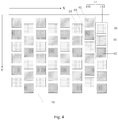
- an embodiment of the present invention provides an organic electroluminescent display device; as shown in Fig. 4 , the organic electroluminescent display device comprises a basal substrate 10 and several pixel unit groups 11 arranged in a matrix on the basal substrate 10 (wherein a structural schematic diagram of a pixel unit group is shown in Fig.
- each of the pixel unit groups 11 comprises a first pixel unit subgroup 111 and a second pixel unit subgroup112; the first pixel unit subgroup 111 and the second pixel unit subgroup 112 are arranged along a first direction X adjacent to each other, and comprise sub pixels with three different colors respectively; wherein, the first pixel unit subgroup 111 comprises a sub pixel sequence in an order of a first sub pixel 01, a second sub pixel 02 and a third sub pixel 03 along a second direction Y; the second pixel unit subgroup 112 comprises a sub pixel sequence in an order of the third sub pixel 03, the first sub pixel 01 and the second sub pixel 02 along the second direction; in the same pixel unit group 11, the component y of the distance between centers of two adjacent first sub pixels 01 respectively located in the first pixel unit subgroup 111 and the second pixel unit subgroup 112 in the second direction Y, the component y of the distance between centers of two adjacent second sub pixels 02 respectively located in the first pixel unit subgroup 11
- each of the pixel unit groups comprises a first pixel unit subgroup and a second pixel unit subgroup; the first pixel unit subgroup and the second pixel unit subgroup are arranged along a first direction adjacent to each other, and comprise sub pixels with three different colors respectively; wherein the first pixel unit subgroup comprises a sub pixel sequence in an order of a first sub pixel, a second sub pixel and a third sub pixel along a second direction; the second pixel unit subgroup comprises a sub pixel sequence in an order of the third sub pixel, the first sub pixel and the second sub pixel along the second direction; in the same pixel unit group, the component of the distance between centers of two adjacent first sub pixels respectively located in the first pixel unit subgroup and the second pixel unit subgroup in the second direction, the component of the distance between centers of two adjacent second sub pixels respectively located in the first pixel unit subgroup and the second pixel unit subgroup in the second direction, and the component of the distance between the distance between
- the regular staggered arrangement of sub pixels with the same color on the basal substrate can be ensured.
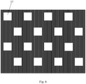
- Fig. 6 which shows a schematic diagram of the openings in a metal mask plate corresponding to the sub pixels with the same color
- the distance between adjacent openings 12 corresponding to the sub pixels with the same color in the metal mask plate can be relatively large, and the distance between adjacent openings 12 corresponding to the sub pixels with different colors in the metal mask plate can be relatively uniform, improving the strength of the metal mask plate; this is beneficial for manufacturing small-sized sub pixels, thereby further improving the resolution of the organic electroluminescent display device.
- the distance between centers of two adjacent sub pixels is constant, i.e., the components z in the second direction Y are the same.
- the sub pixels with the same color have the same size. Since the sub pixels with the same color have the same size, the difficulty of manufacturing the metal mask plate can be further reduced.
- the first direction is perpendicular to the second direction.
- the examples are all illustrated with the first direction being perpendicular to the second direction.
- the row direction or the column direction of the organic electroluminescent display device can be selected as the first direction; the column direction or the row direction of the organic electroluminescent display device can be selected as the second direction.
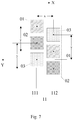
- the component x of the distance between centers of two adjacent sub pixels with the same color respectively located in the first pixel unit subgroup 111 and the second pixel unit subgroup 112 in the first direction is equal to or less than 3/4 of the component y thereof in the second direction.
- the first pixel unit subgroup and the second pixel unit subgroup share sub pixel(s) (e.g., any two adjacent sub pixels in the first pixel unit subgroup share a sub pixel in the second pixel unit subgroup with a different color from those of the two adjacent sub pixels; any two adjacent sub pixels in the second pixel unit subgroup share a sub pixel in the first pixel unit subgroup with a different color from those of the two adjacent sub pixels), thereby improving the virtual display resolution of the screen.
- N is an integer equal to or greater than 2
- the number of pixels can be increased to 3N/2 when the method of sharing sub pixels in the same pixel unit group is applied in the organic electroluminescent display device of the present invention.
- the first sub pixel, the second sub pixel and the third sub pixel are selected from a group comprising red (R) sub pixel, green (G) sub pixel and blue (B) sub pixel.
- the first sub pixel can be one of a red (R) sub pixel, green (G) sub pixel and blue (B) sub pixel
- the second sub pixel can be one of a red (R) sub pixel, green (G) sub pixel and blue (B) sub pixel
- the first sub pixel can be one of a red (R) sub pixel, green (G) sub pixel and blue (B) sub pixel; moreover, the colors of the first sub pixel, the second sub pixel and the third sub pixel are all different.
- the organic electroluminescent display device in the same pixel unit group, all the sub pixels have the same size.
- the arrangement of the sub pixels with the same color presents the same regularity; moreover, the size of the pixels are the same, i.e., the regularities for the arrangements of the three types of the sub pixels with different colors are the same. Therefore, the same one metal mask plate can be used during the manufacture of the sub pixels with different colors, thereby reducing the production quantity of the metal mask plate.
- the size of the red (R) sub pixel is same with the size of the green (G) sub pixel; the size of the blue (B) sub pixel is larger than the size of the red (R) sub pixel. Since the lifetime of the blue luminescent material for manufacturing the blue (B) sub pixel is generally the lowest, the lifetime of the organic electroluminescent display device mainly depends on that of the blue (B) sub pixel.
- the brightness of the blue (B) sub pixel can be reduced when size of the blue (B) sub pixel is increased.
- the lifetime of the blue sub pixels can be prolonged, thereby prolonging the lifetime of the organic electroluminescent display device.
- pixel circuits are required for driving the sub pixels to emit light.
- the pixel circuit is generally located below the light emitting layer, and the pixel circuit is electrically connected with the anode of the corresponding sub pixel through a contact hole on a planarization layer over the pixel circuit.
- the size of the third sub pixel 03 is smaller than the size of the first sub pixel 01 and the size of the second sub pixel 02 respectively. Since the third sub pixel 03 is the smallest, contact holes can be arranged on both sides of the third sub pixel 03.
- each of the pixel unit groups 11 further comprises contact holes one-to-one corresponding to the sub pixels and pixel circuits (not shown in Fig.
- each of the sub pixels being connected to a corresponding pixel circuit through a corresponding contact hole;
- a first contact hole V1 is located between the first sub pixel 01 and the second sub pixel 02, a second contact hole V2 and a third contact hole V3 are respectively located on both sides of the third sub pixel 03 in the first direction X;
- a fourth contact hole V4 is located between the first sub pixel 01 and the second sub pixel 02, a fifth contact hole V5 and a sixth contact hole V6 are respectively located on both sides of the third sub pixel 03 in the first direction X;
- the first contact hole V1, the fifth contact hole V5 and the sixth contact hole V6 are aligned in the first direction X;
- the second contact hole V2, the third contact hole V3 and the fourth contact hole V4 are aligned in the first direction X;
- the first contact hole V1 and the second contact hole V2 are aligned in the second direction Y;
- the first contact hole corresponds to one of two sub pixels adjacent to the first contact hole in the first pixel unit subgroup; the other one of these two sub pixels adjacent to the first contact hole corresponds to the fifth contact hole; the second contact hole corresponds to the third sub pixel in the first pixel unit subgroup; the fourth contact hole corresponds to one of two sub pixels adjacent to the fourth contact hole in the second pixel unit subgroup; the other one of these two sub pixels adjacent to the fourth contact hole corresponds to the third contact hole; the sixth contact hole corresponds to the third sub pixel in the second pixel unit subgroup.
- the sizes of the contact holes are the same.
- the third sub pixel 03 is a green (G) sub pixel.
- the size of the green sub pixel is smaller than the size of the red sub pixel and the size of the blue sub pixel respectively.
- the third sub pixel 03 comprises a first portion 031 extending along the second direction Y, and an extending part 032 extending along the first direction X from the first portion 031; wherein the wording "along a direction" can also be construed as "substantially parallel to a direction"; in the first pixel unit subgroup 111, the second contact hole V2 and the third contact hole V3 are respectively located on both sides of the first part 031 of the third sub pixel 03; and the extending part 032 of the third sub pixel 03 is at least located on a side of the second contact hole V2; in the second pixel unit subgroup 112, the fifth contact hole V5 and the sixth contact hole V6 are respectively located on both sides of the first part 031 of the third sub pixel 03; and the extending part 032 of the third
- the size of the blue (B) sub pixel is larger than the size of the red (R) sub pixel.
- the size of the blue (B) sub pixel is equal to the size of the red (R) sub pixel.
- the shape of each sub pixel is rectangle, which is not limited herein.
- an embodiment of the present invention provides a driving method for any one of the above mentioned organic electroluminescent display devices, wherein the driving method comprises: in the same pixel unit group, the first pixel unit subgroup and the second pixel unit subgroup share at least one sub pixel.
- the first sub pixel in the first pixel unit subgroup and the second sub pixel in the second pixel unit subgroup share the third sub pixel in the second pixel unit subgroup; or, the second sub pixel and the third sub pixel in the first pixel unit subgroup share the first sub pixel in the second pixel unit subgroup; or, the first sub pixel and the second sub pixel in the second pixel unit subgroup share the third sub pixel in the first pixel unit subgroup; or, the first sub pixel and the third sub pixel in the second pixel unit subgroup share the second sub pixel in the first pixel unit subgroup.
- N is an integer equal to or greater than 2
- the number of pixels can be increased to 3N/2, thereby improving the virtual display resolution of the screen.
- the driving method provided by the embodiment of the present invention can improve the virtual display resolution of the screen, with the number of the original pixels being increased to 3/2 times.
- an embodiment of the present invention provides a display device, wherein the display device comprises any one of the above mentioned organic electroluminescent display devices.
- the display device can be any product or component with display function, such as mobile phone, tablet computer, TV, display, notebook computer, digital photo frame, navigator and so on.
- Other essential parts for the display device should be construed as be comprised in the display device, which are not repeated herein, and can not be used to limit the present invention.
- the implementation of the display device can refer to the embodiments of the above mentioned organic electroluminescent display devices, which will not be repeated herein.
- each of the pixel unit groups comprises a first pixel unit subgroup and a second pixel unit subgroup; the first pixel unit subgroup and the second pixel unit subgroup are arranged along a first direction adjacent to each other, and comprise sub pixels with three different colors respectively; wherein the first pixel unit subgroup comprises a sub pixel sequence in an order of a first sub pixel, a second sub pixel and a third sub pixel along a second direction; the second pixel unit subgroup comprises a sub pixel sequence in an order of the third sub pixel, the first sub pixel and the second sub pixel along the second direction; in the same pixel unit group, the component of the distance between centers of two adjacent first sub pixels respectively located in the first pixel unit subgroup and the second pixel unit subgroup in the second direction, the component of the distance between centers of two adjacent second sub pixels respectively located in the first pixel unit subgroup and the second pixel unit subgroup in the second direction, the component of the distance between centers of two adjacent second sub pixels respectively located in the first pixel unit subgroup and
- the regular staggered arrangement of sub pixels with the same color on the basal substrate can be ensured.
- the distance between adjacent openings corresponding to the sub pixels with the same color in the metal mask plate can be relatively large, improving the strength of the metal mask plate; this is beneficial for manufacturing small-sized sub pixels, thereby further improving the resolution of the organic electroluminescent display device.
- the embodiments of the present invention provide an organic electroluminescent display device, a driving method thereof and a display device.
- Each of the pixel unit groups comprises a first pixel unit subgroup and a second pixel unit subgroup; the first pixel unit subgroup and the second pixel unit subgroup are arranged along a first direction adjacent to each other, and comprise sub pixels with three different colors respectively; wherein the first pixel unit subgroup comprises a sub pixel sequence in an order of a first sub pixel, a second sub pixel and a third sub pixel along a second direction; the second pixel unit subgroup comprises a sub pixel sequence in an order of the third sub pixel, the first sub pixel and the second sub pixel along the second direction; in the same pixel unit group, the component of the distance between centers of two adjacent first sub pixels respectively located in the first pixel unit subgroup and the second pixel unit subgroup in the second direction, the component of the distance between centers of two adjacent second sub pixels respectively located in the first pixel unit subgroup and the second pixel unit sub
- the regular staggered arrangement of sub pixels with the same color on the basal substrate can be ensured.
- the distance between adjacent openings corresponding to the sub pixels with the same color in the metal mask plate can be relatively large, improving the strength of the metal mask plate; this is beneficial for manufacturing small-sized sub pixels, thereby further improving the resolution of the organic electroluminescent display device.
Landscapes
- Engineering & Computer Science (AREA)
- Physics & Mathematics (AREA)
- Computer Hardware Design (AREA)
- General Physics & Mathematics (AREA)
- Theoretical Computer Science (AREA)
- Manufacturing & Machinery (AREA)
- Crystallography & Structural Chemistry (AREA)
- Chemical & Material Sciences (AREA)
- Microelectronics & Electronic Packaging (AREA)
- Geometry (AREA)
- Electroluminescent Light Sources (AREA)
- Devices For Indicating Variable Information By Combining Individual Elements (AREA)
- Control Of El Displays (AREA)
- Control Of Indicators Other Than Cathode Ray Tubes (AREA)
Abstract
Description
- The present invention relates to the technical field of display, in particular to an organic electroluminescent display device, a driving method thereof and a display device.
- Organic light emitting diode (OLED) is one of the hot spots in the research of flat panel display today. Compared with liquid crystal display, the OLED display device has the advantages of low energy consumption, low production cost, self luminous, wide viewing angle, quick response and so on. At present, in the flat panel display field of mobile phone, PDA, digital cameras and so on, OLED display device has begun to replace the traditional liquid crystal display (LCD).
- The structure of an OLED display device mainly comprises: a basal substrate, and pixels arranged in a matrix formed on the basal substrate. Wherein the pixels are organic electroluminescent structures typically formed at corresponding pixel positions in an array substrate with organic material, by applying evaporation film technology through a high precision metal mask plate. In order to perform color display, an OLED display should be colorized. The best color image effect can be achieved with a side-by-side arrangement. The side-by-side arrangement refers to three sub pixels of red, green, blue (G, R, B) arranged in a range of one pixel, each sub pixel has a separate organic electroluminescent structure. due to the difference in the organic electroluminescent materials of red, green and blue sub pixels, in the production process, a metal mask plate is required for evaporation of three different organic electroluminescent materials for the red, green and blue sub-pixels (of three primary colors) at corresponding positions, and then adjust the color blending of these three colors, realizing true color.
- The key point for manufacturing OLED display device with high resolution (PPI) is high precise metal mask plate, which is precise and has a good mechanical stability; while the key point for high precise metal mask plate lies in the arrangement of pixels and sub pixels.
- Currently, in an existing OLED display device, the arrangement of the pixel array is typically a side-by-side arrangement. As shown in
Fig. 1 , the OLED display device comprises abasal substrate 1, andpixel units 2 arranged in an array on thebasal substrate 1; apixel unit 2 comprises three parallel sub pixels of red (R), green (G), and blue (B). In order to form the arrangement of the pixel, a corresponding metal mask plate is shown inFig. 2. Fig. 2 schematically shows a metal mask plate used for forming a sub pixel (R sub pixel) in the pixel arrangement shown inFig. 1 . Since the patterns of the sub pixels are the same, a metal mask plate with the same structure can be used to form other sub pixels (G, B). - In
Fig. 2 , a metal mask plate comprises ametal substrate 3 andrectangular openings 4 on themetal substrate 3. Since the sub pixels in a same column in the display device share a same opening, the length of the opening 4 in the metal mask plate is long. For low resolution display device, since the number of pixels is small, the width of the metal strip betweenadjacent openings 4 on the metal mask plate is wide; therefore the production, application and management of such metal mask plates is simple. However, with the increase of the display resolution, the width of the metal strip between adjacent openings in the metal mask plate is smaller, which causes that the metal strip between adjacent openings in the metal mask plate is easily deformed by external influence during the using process, resulting in color mixing due to the cross contamination of the organic electroluminescent materials with different colors in the sub pixels, causing a low yield rate of the product. - In view of the above problems, a metal mask plate shown in
Fig. 3 is proposed, to form a pixel arrangement as shown inFig. 1 . As shown inFig. 3 , the metal mask plate is provided by addingmetal lapping bridges 5 at positions between adjacent sub pixels shown inFig. 1 to the metal mask plate as shown inFig. 2 , to connect adjacent metal strips, modifying aopening 4 shown inFig. 2 intoopenings 6 corresponding to the sub pixels shown inFig. 1 . Although the method can make the shape of the metal strips in the metal mask plate more stable, in order to avoid masking effect of the metal lapping bridges to the sub pixels, a sufficient distance should be kept between the sub pixels and the metal lapping bridges, which can reduce the size of the sub pixels, thus affecting the opening rate of the OLED display device. - To this end, the embodiments of the present invention provide an organic electroluminescent display device, a driving method thereof and a display device, to provide an organic electroluminescent display device with a new pixel arrangement, achieving a metal mask plate with simple manufacture and high mechanical stability, thereby improving the production efficiency of high resolution organic electroluminescent display device, reducing production costs.
- Therefore, an embodiment of the present invention provides an organic electroluminescent display device; the organic electroluminescent display device comprises a basal substrate and several pixel unit groups arranged in a matrix on the basal substrate; each of the pixel unit groups comprises a first pixel unit subgroup and a second pixel unit subgroup; the first pixel unit subgroup and the second pixel unit subgroup are arranged along a first direction adjacent to each other, and comprise sub pixels with three different colors respectively; wherein,
the first pixel unit subgroup comprises a sub pixel sequence in an order of a first sub pixel, a second sub pixel and a third sub pixel along a second direction;
the second pixel unit subgroup comprises a sub pixel sequence in an order of the third sub pixel, the first sub pixel and the second sub pixel along the second direction;
in the same pixel unit group, the component of the distance between centers of two adjacent first sub pixels respectively located in the first pixel unit subgroup and the second pixel unit subgroup in the second direction, the component of the distance between centers of two adjacent second sub pixels respectively located in the first pixel unit subgroup and the second pixel unit subgroup in the second direction, and the component of the distance between centers of two adjacent third sub pixels respectively located in the first pixel unit subgroup and the second pixel unit subgroup in the second direction, are all equal. - Preferably, in the organic electroluminescent display device provided by the embodiment of the present invention, in the same pixel unit subgroup, the distance between centers of two adjacent sub pixels is constant.
- Preferably, in the organic electroluminescent display device provided by the embodiment of the present invention, the sub pixels with the same color have the same size.
- Preferably, in the organic electroluminescent display device provided by the embodiment of the present invention, the first direction is perpendicular to the second direction.
- Preferably, to improve the resolution, in the same pixel unit group, the component of the distance between centers of two adjacent sub pixels with the same color respectively located in the first pixel unit subgroup and the second pixel unit subgroup in the first direction is equal to or less than 3/4 of the component thereof in the second direction.
- Preferably, in the organic electroluminescent display device provided by the embodiment of the present invention, the first sub pixel, the second sub pixel and the third sub pixel are selected from a group comprising red sub pixel, green sub pixel and blue sub pixel.
- Preferably, in order to reduce the production quantity of the metal mask plate, in the organic electroluminescent display device provided by the embodiment of the present invention, in the same pixel unit group, all the sub pixels have the same size.
- Preferably, in order to prolong the lifetime of the organic electroluminescent display device, in the organic electroluminescent display device provided by the embodiment of the present invention, in the same pixel unit group, the size of the red sub pixel is same with the size of the green sub pixel; the size of the blue sub pixel is larger than the size of the red sub pixel.
- Preferably, in order to facilitate the arrangement of contact holes connecting each sub pixel and the corresponding pixel circuit on the basal substrate, in the organic electroluminescent display device provided by the embodiment of the present invention, the size of the third sub pixel is smaller than the size of the first sub pixel and the size of the second sub pixel respectively.
- Further, to ensure the resolution of the organic electroluminescent display device, and in order to facilitate the arrangement of contact holes connecting each sub pixel and the corresponding pixel circuit on the basal substrate, in the organic electroluminescent display device provided by the embodiment of the present invention, in the same pixel unit group:
- the component of the distance between centers of two adjacent third sub pixels respectively located in the first pixel unit subgroup and the second pixel unit subgroup in the first direction is less than 3/4 of the component thereof in the second direction;
- the component of the distance between centers of two adjacent first sub pixels respectively located in the first pixel unit subgroup and the second pixel unit subgroup in the first direction is equal to 3/4 of the component thereof in the second direction;
- the component of the distance between centers of two adjacent second sub pixels respectively located in the first pixel unit subgroup and the second pixel unit subgroup in the first direction is equal to 3/4 of the component thereof in the second direction.
- Particularly, in order to facilitate the arrangement of contact holes connecting each sub pixel and the corresponding pixel circuit on the basal substrate, in the organic electroluminescent display device provided by the embodiment of the present invention, each of the pixel unit groups further comprises contact holes one-to-one corresponding to the sub pixels and pixel circuits, each of the sub pixels being connected to a corresponding pixel circuit through a corresponding contact hole; wherein,
in the first pixel unit subgroup, a first contact hole is located between the first sub pixel and the second sub pixel, a second contact hole and a third contact hole are respectively located on both sides of the third sub pixel in the first direction;
in the second pixel unit subgroup, a fourth contact hole is located between the first sub pixel and the second sub pixel, a fifth contact hole and a sixth contact hole are respectively located on both sides of the third sub pixel in the first direction;
the first contact hole, the fifth contact hole and the sixth contact hole are aligned in the first direction; the second contact hole, the third contact hole and the fourth contact hole are aligned in the first direction; the first contact hole and the second contact hole are aligned in the second direction; the fifth contact hole and the third contact hole are aligned in the second direction; the sixth contact hole and the fourth contact hole are aligned in the second direction. In such a manner, the contact holes on the basal substrate are arranged in a matrix, thereby reducing the difficulty of back board wiring in the organic electroluminescent display device. - Preferably, in order to ensure the display effect of the organic electroluminescent display device, in the organic electroluminescent display device provided by the embodiment of the present invention, the third sub pixel is a green sub pixel.
- Preferably, in order to ensure a good aperture ratio for the organic electroluminescent display device, in the organic electroluminescent display device provided by the embodiment of the present invention, the third sub pixel comprises a first portion extending along the second direction, and an extending part extending along the first direction from the first portion;
in the first pixel unit subgroup, the second contact hole and the third contact hole are respectively located on both sides of the first part of the third sub pixel; and the extending part of the third sub pixel is at least located on a side of the second contact hole;
in the second pixel unit subgroup, the fifth contact hole and the sixth contact hole are respectively located on both sides of the first part of the third sub pixel; and the extending part of the third sub pixel is at least located on a side of the sixth contact hole. - Preferably, in order to reduce the production quantity of the metal mask plate, in the organic electroluminescent display device provided by the embodiment of the present invention, the size of the blue sub pixel is larger than the size of the red sub pixel.
- Preferably, in order to ensure the lifetime of the organic electroluminescent display device, in the organic electroluminescent display device provided by the embodiment of the present invention, the size of the blue sub pixel is equal to the size of the red sub pixel.
- Preferably, in order to facilitate the implementation, in the organic electroluminescent display device provided by the embodiment of the present invention, the shape of each sub pixel is rectangle.
- Accordingly, an embodiment of the present invention provides a driving method for any one of the above mentioned organic electroluminescent display devices, wherein the driving method comprises: in the same pixel unit group, the first pixel unit subgroup and the second pixel unit subgroup share at least one sub pixel.
- Accordingly, an embodiment of the present invention provides a display device, wherein the display device comprises any one of the above mentioned organic electroluminescent display devices.
- According to the organic electroluminescent display device, the driving method thereof and the display device provided by the embodiments of the present invention, each of the pixel unit groups comprises a first pixel unit subgroup and a second pixel unit subgroup; the first pixel unit subgroup and the second pixel unit subgroup are arranged along a first direction adjacent to each other, and comprise sub pixels with three different colors respectively; wherein the first pixel unit subgroup comprises a sub pixel sequence in an order of a first sub pixel, a second sub pixel and a third sub pixel along a second direction; the second pixel unit subgroup comprises a sub pixel sequence in an order of the third sub pixel, the first sub pixel and the second sub pixel along the second direction; in the same pixel unit group, the component of the distance between centers of two adjacent first sub pixels respectively located in the first pixel unit subgroup and the second pixel unit subgroup in the second direction, the component of the distance between centers of two adjacent second sub pixels respectively located in the first pixel unit subgroup and the second pixel unit subgroup in the second direction, and the component of the distance between centers of two adjacent third sub pixels respectively located in the first pixel unit subgroup and the second pixel unit subgroup in the second direction, are all equal. In such a manner, the regular staggered arrangement of sub pixels with the same color on the basal substrate can be ensured. During the manufacture of a corresponding metal mask plate, the distance between adjacent openings corresponding to the sub pixels with the same color in the metal mask plate can be relatively large, improving the strength of the metal mask plate; this is beneficial for manufacturing small-sized sub pixels, thereby further improving the resolution of the organic electroluminescent display device.
-
-
Fig. 1 is a structural schematic diagram of a pixel arrangement in an existing organic electroluminescent display device; -
Fig. 2 shows a metal mask plate used for manufacturing an organic electroluminescent display device shown inFig. 1 ; -
Fig. 3 shows another metal mask plate used for manufacturing an organic electroluminescent display device shown inFig. 1 ; -
Fig. 4 is a first structural schematic diagram of an organic electroluminescent display device provided by an embodiment of the present invention; -
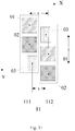
Fig. 5 is a first structural schematic diagram of a pixel unit group in the organic electroluminescent display device provided by an embodiment of the present invention; -
Fig. 6 shows a metal mask plate used for manufacturing an organic electroluminescent display device shown inFig. 4 ; -
Fig. 7 is a second structural schematic diagram of another pixel unit group in the organic electroluminescent display device provided by an embodiment of the present invention; -
Fig. 8 is a second structural schematic diagram of an organic electroluminescent display device provided by an embodiment of the present invention; -
Fig. 9 is a third structural schematic diagram of an organic electroluminescent display device provided by an embodiment of the present invention; -
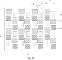
Fig. 10 is a fourth structural schematic diagram of an organic electroluminescent display device provided by an embodiment of the present invention; -
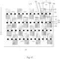
Fig. 11 is a third structural schematic diagram of another pixel unit group in the organic electroluminescent display device provided by an embodiment of the present invention; -
Fig. 12 is a fifth structural schematic diagram of an organic electroluminescent display device provided by an embodiment of the present invention; -
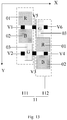
Fig. 13 is a fourth structural schematic diagram of another pixel unit group in the organic electroluminescent display device provided by an embodiment of the present invention; -
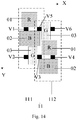
Fig. 14 is a fifth structural schematic diagram of another pixel unit group in the organic electroluminescent display device provided by an embodiment of the present invention; -
Fig. 15 is a sixth structural schematic diagram of another pixel unit group in the organic electroluminescent display device provided by an embodiment of the present invention; -
Fig. 16 is a seventh structural schematic diagram of another pixel unit group in the organic electroluminescent display device provided by an embodiment of the present invention. - In the following, the implementations of the organic electroluminescent display device, the driving method thereof and the display device provided by the embodiments of the invention will be described clearly and completely in connection with the drawings.
- The shapes and thickness of the film layer in the drawings do not reflect the real scale of the organic electroluminescent display device, but to schematically illustrate the content of the invention.
- An embodiment of the present invention provides an organic electroluminescent display device; as shown in
Fig. 4 , the organic electroluminescent display device comprises abasal substrate 10 and severalpixel unit groups 11 arranged in a matrix on the basal substrate 10 (wherein a structural schematic diagram of a pixel unit group is shown inFig. 5 ); each of thepixel unit groups 11 comprises a firstpixel unit subgroup 111 and a second pixel unit subgroup112; the firstpixel unit subgroup 111 and the secondpixel unit subgroup 112 are arranged along a first direction X adjacent to each other, and comprise sub pixels with three different colors respectively; wherein,
the firstpixel unit subgroup 111 comprises a sub pixel sequence in an order of afirst sub pixel 01, asecond sub pixel 02 and athird sub pixel 03 along a second direction Y;
the secondpixel unit subgroup 112 comprises a sub pixel sequence in an order of thethird sub pixel 03, thefirst sub pixel 01 and thesecond sub pixel 02 along the second direction;
in the samepixel unit group 11, the component y of the distance between centers of two adjacentfirst sub pixels 01 respectively located in the firstpixel unit subgroup 111 and the secondpixel unit subgroup 112 in the second direction Y, the component y of the distance between centers of two adjacentsecond sub pixels 02 respectively located in the firstpixel unit subgroup 111 and the secondpixel unit subgroup 112 in the second direction Y, and the component y of the distance between centers of two adjacentthird sub pixels 03 respectively located in the firstpixel unit subgroup 111 and the secondpixel unit subgroup 112 in the second direction Y, are all equal. - In the organic electroluminescent display device provided by the embodiment of the present invention, each of the pixel unit groups comprises a first pixel unit subgroup and a second pixel unit subgroup; the first pixel unit subgroup and the second pixel unit subgroup are arranged along a first direction adjacent to each other, and comprise sub pixels with three different colors respectively; wherein the first pixel unit subgroup comprises a sub pixel sequence in an order of a first sub pixel, a second sub pixel and a third sub pixel along a second direction; the second pixel unit subgroup comprises a sub pixel sequence in an order of the third sub pixel, the first sub pixel and the second sub pixel along the second direction; in the same pixel unit group, the component of the distance between centers of two adjacent first sub pixels respectively located in the first pixel unit subgroup and the second pixel unit subgroup in the second direction, the component of the distance between centers of two adjacent second sub pixels respectively located in the first pixel unit subgroup and the second pixel unit subgroup in the second direction, and the component of the distance between centers of two adjacent third sub pixels respectively located in the first pixel unit subgroup and the second pixel unit subgroup in the second direction, are all equal. In such a manner, the regular staggered arrangement of sub pixels with the same color on the basal substrate can be ensured. During the manufacture of a corresponding metal mask plate, as shown in
Fig. 6 (which shows a schematic diagram of the openings in a metal mask plate corresponding to the sub pixels with the same color), the distance betweenadjacent openings 12 corresponding to the sub pixels with the same color in the metal mask plate can be relatively large, and the distance betweenadjacent openings 12 corresponding to the sub pixels with different colors in the metal mask plate can be relatively uniform, improving the strength of the metal mask plate; this is beneficial for manufacturing small-sized sub pixels, thereby further improving the resolution of the organic electroluminescent display device. - Preferably, in the organic electroluminescent display device provided by the embodiment of the present invention, as shown in
Fig. 5 , in the same pixel unit subgroup, the distance between centers of two adjacent sub pixels is constant, i.e., the components z in the second direction Y are the same. - Preferably, in the organic electroluminescent display device provided by the embodiment of the present invention, as shown in
Fig. 5 , the sub pixels with the same color have the same size. Since the sub pixels with the same color have the same size, the difficulty of manufacturing the metal mask plate can be further reduced. - Preferably, in the organic electroluminescent display device provided by the embodiment of the present invention, the first direction is perpendicular to the second direction. In the embodiments of the present invention, the examples are all illustrated with the first direction being perpendicular to the second direction.
- Particularly, in an implementation, the row direction or the column direction of the organic electroluminescent display device can be selected as the first direction; the column direction or the row direction of the organic electroluminescent display device can be selected as the second direction.
- Preferably, in the organic electroluminescent display device provided by the embodiment of the present invention, as shown in
Fig. 7 , in the same pixel unit group, the component x of the distance between centers of two adjacent sub pixels with the same color respectively located in the firstpixel unit subgroup 111 and the secondpixel unit subgroup 112 in the first direction is equal to or less than 3/4 of the component y thereof in the second direction. By reducing the width of each pixel unit group in the first direction, the number of pixel unit groups on the display device can be increased, thereby improving the pixel resolution. Further, in the same pixel unit group, the first pixel unit subgroup and the second pixel unit subgroup share sub pixel(s) (e.g., any two adjacent sub pixels in the first pixel unit subgroup share a sub pixel in the second pixel unit subgroup with a different color from those of the two adjacent sub pixels; any two adjacent sub pixels in the second pixel unit subgroup share a sub pixel in the first pixel unit subgroup with a different color from those of the two adjacent sub pixels), thereby improving the virtual display resolution of the screen. For example, when the original number of pixels is N, N is an integer equal to or greater than 2, the number of pixels can be increased to 3N/2 when the method of sharing sub pixels in the same pixel unit group is applied in the organic electroluminescent display device of the present invention. - Preferably, in the organic electroluminescent display device provided by the embodiment of the present invention, the first sub pixel, the second sub pixel and the third sub pixel are selected from a group comprising red (R) sub pixel, green (G) sub pixel and blue (B) sub pixel. In the embodiments of the present invention, the first sub pixel can be one of a red (R) sub pixel, green (G) sub pixel and blue (B) sub pixel, the second sub pixel can be one of a red (R) sub pixel, green (G) sub pixel and blue (B) sub pixel, the first sub pixel can be one of a red (R) sub pixel, green (G) sub pixel and blue (B) sub pixel; moreover, the colors of the first sub pixel, the second sub pixel and the third sub pixel are all different.
- Further, in order to reduce the production quantity of the metal mask plate, in the organic electroluminescent display device provided by the embodiment of the present invention, in the same pixel unit group, all the sub pixels have the same size. In such a manner, in the organic electroluminescent display device, the arrangement of the sub pixels with the same color presents the same regularity; moreover, the size of the pixels are the same, i.e., the regularities for the arrangements of the three types of the sub pixels with different colors are the same. Therefore, the same one metal mask plate can be used during the manufacture of the sub pixels with different colors, thereby reducing the production quantity of the metal mask plate.
- Preferably, in order to prolong the lifetime of the organic electroluminescent display device, in the organic electroluminescent display device provided by the embodiment of the present invention, as shown in
Fig. 8 , in the same pixel unit group, the size of the red (R) sub pixel is same with the size of the green (G) sub pixel; the size of the blue (B) sub pixel is larger than the size of the red (R) sub pixel. Since the lifetime of the blue luminescent material for manufacturing the blue (B) sub pixel is generally the lowest, the lifetime of the organic electroluminescent display device mainly depends on that of the blue (B) sub pixel. To achieve the same display brightness, the brightness of the blue (B) sub pixel can be reduced when size of the blue (B) sub pixel is increased. By decreasing the current density flowing through the blue (B) sub pixels, the lifetime of the blue sub pixels can be prolonged, thereby prolonging the lifetime of the organic electroluminescent display device. - Particularly, to enable the light emitting of the sub pixels in the organic electroluminescent display device, pixel circuits are required for driving the sub pixels to emit light. The pixel circuit is generally located below the light emitting layer, and the pixel circuit is electrically connected with the anode of the corresponding sub pixel through a contact hole on a planarization layer over the pixel circuit.
- Therefore, preferably, in the organic electroluminescent display device provided by the embodiment of the present invention, as shown in
Fig. 9 andFig. 10 , the size of thethird sub pixel 03 is smaller than the size of thefirst sub pixel 01 and the size of thesecond sub pixel 02 respectively. Since thethird sub pixel 03 is the smallest, contact holes can be arranged on both sides of thethird sub pixel 03. - Further, in order to facilitate the manufacture of contact holes connecting each sub pixel and the corresponding pixel circuit on the basal substrate, in the organic electroluminescent display device provided by the embodiment of the present invention, as shown in
Fig. 11 , in the same pixel unit group 11: - the component x of the distance between centers of two adjacent
third sub pixels 03 respectively located in the firstpixel unit subgroup 111 and the secondpixel unit subgroup 112 in the first direction X is less than 3/4 of the component x thereof in the second direction; - the component of the distance between centers of two adjacent
first sub pixels 01 respectively located in the firstpixel unit subgroup 111 and the secondpixel unit subgroup 112 in the first direction X is equal to 3/4 of the component y thereof in the second direction; - the component of the distance between centers of two adjacent
second sub pixels 02 respectively located in the firstpixel unit subgroup 111 and the secondpixel unit subgroup 112 in the first direction X is equal to 3/4 of the component y thereof in the second direction. - Particularly, in the organic electroluminescent display device provided by the embodiment of the present invention, as shown in
Fig. 12 , each of thepixel unit groups 11 further comprises contact holes one-to-one corresponding to the sub pixels and pixel circuits (not shown inFig. 12 ), each of the sub pixels being connected to a corresponding pixel circuit through a corresponding contact hole; wherein,
in the firstpixel unit subgroup 111, a first contact hole V1 is located between thefirst sub pixel 01 and thesecond sub pixel 02, a second contact hole V2 and a third contact hole V3 are respectively located on both sides of thethird sub pixel 03 in the first direction X;
in the secondpixel unit subgroup 112, a fourth contact hole V4 is located between thefirst sub pixel 01 and thesecond sub pixel 02, a fifth contact hole V5 and a sixth contact hole V6 are respectively located on both sides of thethird sub pixel 03 in the first direction X;
the first contact hole V1, the fifth contact hole V5 and the sixth contact hole V6 are aligned in the first direction X; the second contact hole V2, the third contact hole V3 and the fourth contact hole V4 are aligned in the first direction X; the first contact hole V1 and the second contact hole V2 are aligned in the second direction Y; the fifth contact hole V5 and the third contact hole V3 are aligned in the second direction Y; the sixth contact hole V6 and the fourth contact hole V4 are aligned in the second direction Y. In such a manner, the contact holes on the basal substrate are arranged in a matrix, thereby reducing the difficulty of back board wiring in the organic electroluminescent display device. - It should be noted that, in the organic electroluminescent display device provided by the embodiment of the present invention, in each pixel unit group, the first contact hole corresponds to one of two sub pixels adjacent to the first contact hole in the first pixel unit subgroup; the other one of these two sub pixels adjacent to the first contact hole corresponds to the fifth contact hole; the second contact hole corresponds to the third sub pixel in the first pixel unit subgroup; the fourth contact hole corresponds to one of two sub pixels adjacent to the fourth contact hole in the second pixel unit subgroup; the other one of these two sub pixels adjacent to the fourth contact hole corresponds to the third contact hole; the sixth contact hole corresponds to the third sub pixel in the second pixel unit subgroup.
- Further, to reduce the difficulty in the manufacture, in the organic electroluminescent display device provided by the embodiment of the present invention, the sizes of the contact holes are the same.
- Preferably, in the organic electroluminescent display device provided by the embodiment of the present invention, as shown in
Fig. 13 , according to the lifetime and display effect of the sub pixels with different colors, thethird sub pixel 03 is a green (G) sub pixel. In this way, the size of the green sub pixel is smaller than the size of the red sub pixel and the size of the blue sub pixel respectively. - Further, in order to ensure a good aperture ratio for the organic electroluminescent display device, in the organic electroluminescent display device provided by the embodiment of the present invention, as shown in
Fig. 15 andFig. 16 , thethird sub pixel 03 comprises afirst portion 031 extending along the second direction Y, and an extendingpart 032 extending along the first direction X from thefirst portion 031; wherein the wording "along a direction" can also be construed as "substantially parallel to a direction";
in the firstpixel unit subgroup 111, the second contact hole V2 and the third contact hole V3 are respectively located on both sides of thefirst part 031 of thethird sub pixel 03; and the extendingpart 032 of thethird sub pixel 03 is at least located on a side of the second contact hole V2;
in the secondpixel unit subgroup 112, the fifth contact hole V5 and the sixth contact hole V6 are respectively located on both sides of thefirst part 031 of thethird sub pixel 03; and the extendingpart 032 of thethird sub pixel 03 is at least located on a side of the sixth contact hole V6. Inthis way, the light emitting area of the third sub pixel can be increased without affecting the arrangement of the contact holes, thereby increasing the aperture ratio for the organic electroluminescent display device. - Preferably, in order to reduce the production quantity of the metal mask plate, in the organic electroluminescent display device provided by the embodiment of the present invention, as shown in
Fig. 13 , the size of the blue (B) sub pixel is larger than the size of the red (R) sub pixel. - Or, preferably, in order to ensure the lifetime of the organic electroluminescent display device, in the organic electroluminescent display device provided by the embodiment of the present invention, as shown in
Fig. 14 , the size of the blue (B) sub pixel is equal to the size of the red (R) sub pixel. - Preferably, in the organic electroluminescent display device provided by the embodiment of the present invention, the shape of each sub pixel is rectangle, which is not limited herein.
- Based on the same inventive concept, an embodiment of the present invention provides a driving method for any one of the above mentioned organic electroluminescent display devices, wherein the driving method comprises: in the same pixel unit group, the first pixel unit subgroup and the second pixel unit subgroup share at least one sub pixel. For example, the first sub pixel in the first pixel unit subgroup and the second sub pixel in the second pixel unit subgroup share the third sub pixel in the second pixel unit subgroup; or, the second sub pixel and the third sub pixel in the first pixel unit subgroup share the first sub pixel in the second pixel unit subgroup; or, the first sub pixel and the second sub pixel in the second pixel unit subgroup share the third sub pixel in the first pixel unit subgroup; or, the first sub pixel and the third sub pixel in the second pixel unit subgroup share the second sub pixel in the first pixel unit subgroup. In such a manner, by applying the method of sharing sub pixels for the same pixel unit group, for example, when the original number of pixels is N, N is an integer equal to or greater than 2, the number of pixels can be increased to 3N/2, thereby improving the virtual display resolution of the screen.
- By applying the method of sharing sub pixels for the same pixel unit group, the driving method provided by the embodiment of the present invention can improve the virtual display resolution of the screen, with the number of the original pixels being increased to 3/2 times.
- Based on the same inventive concept, an embodiment of the present invention provides a display device, wherein the display device comprises any one of the above mentioned organic electroluminescent display devices. The display device can be any product or component with display function, such as mobile phone, tablet computer, TV, display, notebook computer, digital photo frame, navigator and so on. Other essential parts for the display device should be construed as be comprised in the display device, which are not repeated herein, and can not be used to limit the present invention. The implementation of the display device can refer to the embodiments of the above mentioned organic electroluminescent display devices, which will not be repeated herein.
- According to the organic electroluminescent display device, the driving method thereof and the display device provided by the embodiments of the present invention, each of the pixel unit groups comprises a first pixel unit subgroup and a second pixel unit subgroup; the first pixel unit subgroup and the second pixel unit subgroup are arranged along a first direction adjacent to each other, and comprise sub pixels with three different colors respectively; wherein the first pixel unit subgroup comprises a sub pixel sequence in an order of a first sub pixel, a second sub pixel and a third sub pixel along a second direction; the second pixel unit subgroup comprises a sub pixel sequence in an order of the third sub pixel, the first sub pixel and the second sub pixel along the second direction; in the same pixel unit group, the component of the distance between centers of two adjacent first sub pixels respectively located in the first pixel unit subgroup and the second pixel unit subgroup in the second direction, the component of the distance between centers of two adjacent second sub pixels respectively located in the first pixel unit subgroup and the second pixel unit subgroup in the second direction, and the component of the distance between centers of two adjacent third sub pixels respectively located in the first pixel unit subgroup and the second pixel unit subgroup in the second direction, are all equal. In such a manner, the regular staggered arrangement of sub pixels with the same color on the basal substrate can be ensured. During the manufacture of a corresponding metal mask plate, the distance between adjacent openings corresponding to the sub pixels with the same color in the metal mask plate can be relatively large, improving the strength of the metal mask plate; this is beneficial for manufacturing small-sized sub pixels, thereby further improving the resolution of the organic electroluminescent display device.
- The embodiments of the present invention provide an organic electroluminescent display device, a driving method thereof and a display device. Each of the pixel unit groups comprises a first pixel unit subgroup and a second pixel unit subgroup; the first pixel unit subgroup and the second pixel unit subgroup are arranged along a first direction adjacent to each other, and comprise sub pixels with three different colors respectively; wherein the first pixel unit subgroup comprises a sub pixel sequence in an order of a first sub pixel, a second sub pixel and a third sub pixel along a second direction; the second pixel unit subgroup comprises a sub pixel sequence in an order of the third sub pixel, the first sub pixel and the second sub pixel along the second direction; in the same pixel unit group, the component of the distance between centers of two adjacent first sub pixels respectively located in the first pixel unit subgroup and the second pixel unit subgroup in the second direction, the component of the distance between centers of two adjacent second sub pixels respectively located in the first pixel unit subgroup and the second pixel unit subgroup in the second direction, and the component of the distance between centers of two adjacent third sub pixels respectively located in the first pixel unit subgroup and the second pixel unit subgroup in the second direction, are all equal. In such a manner, the regular staggered arrangement of sub pixels with the same color on the basal substrate can be ensured. During the manufacture of a corresponding metal mask plate, the distance between adjacent openings corresponding to the sub pixels with the same color in the metal mask plate can be relatively large, improving the strength of the metal mask plate; this is beneficial for manufacturing small-sized sub pixels, thereby further improving the resolution of the organic electroluminescent display device.
- Apparently, the person skilled in the art may make various alterations and variations to the invention without departing the spirit and scope of the invention. As such, provided that these modifications and variations of the invention pertain to the scope of the claims of the invention and their equivalents, the invention is intended to embrace these alterations and variations.
Claims (18)
- An organic electroluminescent display device; wherein the organic electroluminescent display device comprises a basal substrate and several pixel unit groups arranged in a matrix on the basal substrate; each of the pixel unit groups comprises a first pixel unit subgroup and a second pixel unit subgroup; the first pixel unit subgroup and the second pixel unit subgroup are arranged along a first direction adjacent to each other, and comprise sub pixels with three different colors respectively; wherein,
the first pixel unit subgroup comprises a sub pixel sequence in an order of a first sub pixel, a second sub pixel and a third sub pixel along a second direction;
the second pixel unit subgroup comprises a sub pixel sequence in an order of the third sub pixel, the first sub pixel and the second sub pixel along the second direction;
in the same pixel unit group, the component of the distance between centers of two adjacent first sub pixels respectively located in the first pixel unit subgroup and the second pixel unit subgroup in the second direction, the component of the distance between centers of two adjacent second sub pixels respectively located in the first pixel unit subgroup and the second pixel unit subgroup in the second direction, and the component of the distance between centers of two adjacent third sub pixels respectively located in the first pixel unit subgroup and the second pixel unit subgroup in the second direction, are all equal. - The organic electroluminescent display device according to claim 1, wherein in the same pixel unit subgroup, the distance between centers of two adjacent sub pixels is constant.
- The organic electroluminescent display device according to claim 1, wherein the sub pixels with the same color have the same size.
- The organic electroluminescent display device according to claim 1, wherein the first direction is perpendicular to the second direction.
- The organic electroluminescent display device according to claim 1, wherein in the same pixel unit group, the component of the distance between centers of two adjacent sub pixels with the same color respectively located in the first pixel unit subgroup and the second pixel unit subgroup in the first direction is equal to or less than 3/4 of the component thereof in the second direction.
- The organic electroluminescent display device according to any one of claims 1-5, wherein the first sub pixel, the second sub pixel and the third sub pixel are selected from a group comprising red sub pixel, green sub pixel and blue sub pixel.
- The organic electroluminescent display device according to claim 6, wherein in the same pixel unit group, all the sub pixels have the same size.
- The organic electroluminescent display device according to claim 6, wherein in the same pixel unit group, the size of the red sub pixel is same with the size of the green sub pixel; the size of the blue sub pixel is larger than the size of the red sub pixel.
- The organic electroluminescent display device according to claim 6, wherein the size of the third sub pixel is smaller than the size of the first sub pixel and the size of the second sub pixel respectively.
- The organic electroluminescent display device according to claim 9, wherein in the same pixel unit group:the component of the distance between centers of two adjacent third sub pixels respectively located in the first pixel unit subgroup and the second pixel unit subgroup in the first direction is less than 3/4 of the component thereof in the second direction;the component of the distance between centers of two adjacent first sub pixels respectively located in the first pixel unit subgroup and the second pixel unit subgroup in the first direction is equal to 3/4 of the component thereof in the second direction;the component of the distance between centers of two adjacent second sub pixels respectively located in the first pixel unit subgroup and the second pixel unit subgroup in the first direction is equal to 3/4 of the component thereof in the second direction.
- The organic electroluminescent display device according to claim 10, wherein each of the pixel unit groups further comprises contact holes one-to-one corresponding to the sub pixels and pixel circuits, each of the sub pixels being connected to a corresponding pixel circuit through a corresponding contact hole; wherein,
in the first pixel unit subgroup, a first contact hole is located between the first sub pixel and the second sub pixel, a second contact hole and a third contact hole are respectively located on both sides of the third sub pixel in the first direction;
in the second pixel unit subgroup, a fourth contact hole is located between the first sub pixel and the second sub pixel, a fifth contact hole and a sixth contact hole are respectively located on both sides of the third sub pixel in the first direction;
the first contact hole, the fifth contact hole and the sixth contact hole are aligned in the first direction; the second contact hole, the third contact hole and the fourth contact hole are aligned in the first direction; the first contact hole and the second contact hole are aligned in the second direction; the fifth contact hole and the third contact hole are aligned in the second direction; the sixth contact hole and the fourth contact hole are aligned in the second direction. - The organic electroluminescent display device according to claim 11, wherein the third sub pixel is a green sub pixel.
- The organic electroluminescent display device according to claim 11, wherein the third sub pixel comprises a first portion extending along the second direction, and an extending part extending along the first direction from the first portion;
in the first pixel unit subgroup, the second contact hole and the third contact hole are respectively located on both sides of the first part of the third sub pixel; and the extending part of the third sub pixel is at least located on a side of the second contact hole;
in the second pixel unit subgroup, the fifth contact hole and the sixth contact hole are respectively located on both sides of the first part of the third sub pixel; and the extending part of the third sub pixel is at least located on a side of the sixth contact hole. - The organic electroluminescent display device according to claim 12, wherein the size of the blue sub pixel is larger than the size of the red sub pixel.
- The organic electroluminescent display device according to claim 12, wherein the size of the blue sub pixel is equal to the size of the red sub pixel.
- The organic electroluminescent display device according to any one of claims 1-5, wherein the shape of each sub pixel is rectangle.
- A driving method for the organic electroluminescent display device according to any one of claims 1-16, wherein the driving method comprises: in the same pixel unit group, the first pixel unit subgroup and the second pixel unit subgroup share at least one sub pixel.
- A display device, wherein the display device comprises the organic electroluminescent display device according to any one of claims 1-16.
Applications Claiming Priority (2)
| Application Number | Priority Date | Filing Date | Title |
|---|---|---|---|
| CN201410584435.5A CN104319283B (en) | 2014-10-27 | 2014-10-27 | A kind of organic elctroluminescent device, its driving method and display unit |
| PCT/CN2015/072538 WO2016065770A1 (en) | 2014-10-27 | 2015-02-09 | Organic light emitting diode display device, driving method and display apparatus thereof |
Publications (3)
| Publication Number | Publication Date |
|---|---|
| EP3214650A1 true EP3214650A1 (en) | 2017-09-06 |
| EP3214650A4 EP3214650A4 (en) | 2018-07-11 |
| EP3214650B1 EP3214650B1 (en) | 2020-04-29 |
Family
ID=52374492
Family Applications (1)
| Application Number | Title | Priority Date | Filing Date |
|---|---|---|---|
| EP15793670.9A Active EP3214650B1 (en) | 2014-10-27 | 2015-02-09 | Organic light emitting diode display device, driving method and display apparatus thereof |
Country Status (6)
| Country | Link |
|---|---|
| US (1) | US9767741B2 (en) |
| EP (1) | EP3214650B1 (en) |
| JP (1) | JP6495460B2 (en) |
| KR (1) | KR101845644B1 (en) |
| CN (1) | CN104319283B (en) |
| WO (1) | WO2016065770A1 (en) |
Cited By (1)
| Publication number | Priority date | Publication date | Assignee | Title |
|---|---|---|---|---|
| US11302750B2 (en) * | 2017-08-31 | 2022-04-12 | Kunshan Go-Visionox Opto-Electronics Co., Ltd. | Pixel structure and OLED display panel |
Families Citing this family (44)
| Publication number | Priority date | Publication date | Assignee | Title |
|---|---|---|---|---|
| CN104319283B (en) | 2014-10-27 | 2016-03-02 | 京东方科技集团股份有限公司 | A kind of organic elctroluminescent device, its driving method and display unit |
| CN104362170B (en) * | 2014-11-28 | 2017-04-12 | 京东方科技集团股份有限公司 | Organic electroluminescence display appliance and driving method and related device thereof |
| CN104361862A (en) * | 2014-11-28 | 2015-02-18 | 京东方科技集团股份有限公司 | Array substrate, drive method thereof, display panel and display device |
| CN104630703B (en) * | 2015-01-29 | 2017-09-19 | 四川虹视显示技术有限公司 | The mask plate group and substrate of OLED |
| CN104570531A (en) * | 2015-02-05 | 2015-04-29 | 京东方科技集团股份有限公司 | Array substrate and display device |
| CN104635399A (en) * | 2015-03-09 | 2015-05-20 | 京东方科技集团股份有限公司 | Display device and grating control method |
| WO2016145609A1 (en) * | 2015-03-17 | 2016-09-22 | Shenzhen Yunyinggu Technology Co., Ltd. | Subpixel arrangement for displays and driving circuit thereof |
| US10134330B2 (en) | 2015-03-17 | 2018-11-20 | Kunshan Yunyinggu Electronic Technology Co., Ltd. | Subpixel arrangement for displays and driving circuit thereof |
| CN106157876B (en) * | 2015-03-27 | 2019-04-23 | 上海和辉光电有限公司 | The display methods and display of display image |
| CN104835832A (en) * | 2015-05-18 | 2015-08-12 | 京东方科技集团股份有限公司 | Pixel arrangement structure, organic electroluminescent device, display device, and mask plate |
| CN104898369B (en) * | 2015-06-23 | 2019-05-17 | 京东方科技集团股份有限公司 | Display substrate and manufacturing method thereof, and display substrate manufacturing system and display device |
| CN105047092B (en) * | 2015-08-06 | 2018-07-06 | 上海和辉光电有限公司 | Display and its pel array |
| CN105096885B (en) * | 2015-08-28 | 2018-01-02 | 厦门天马微电子有限公司 | Array base palte, display device and sub-pixel rendering intent |
| CN113192459A (en) | 2015-09-02 | 2021-07-30 | 天马微电子股份有限公司 | Display device |
| CN105425485A (en) * | 2015-12-10 | 2016-03-23 | 昆山龙腾光电有限公司 | Display panel sub-pixel arrangement structure and display device |
| US10256222B2 (en) * | 2016-01-05 | 2019-04-09 | Innolux Corporation | Light emitting diode substrate and display apparatus applying the same |
| KR102825728B1 (en) * | 2016-11-30 | 2025-06-26 | 엘지디스플레이 주식회사 | Organic light emitting diode display device |
| CN107221555B (en) * | 2017-06-21 | 2019-02-26 | 深圳市华星光电半导体显示技术有限公司 | OLED display panel and display device |
| CN107436685B (en) * | 2017-07-31 | 2020-07-07 | 京东方科技集团股份有限公司 | Display device, self-luminous display panel and gesture recognition method |
| CN107706211A (en) * | 2017-08-29 | 2018-02-16 | 上海天马有机发光显示技术有限公司 | A kind of display panel and display device |
| CN109427291B (en) * | 2017-08-31 | 2020-09-15 | 昆山国显光电有限公司 | Pixel structure driving method |
| CN109427278B (en) | 2017-08-31 | 2020-07-03 | 昆山国显光电有限公司 | Display panel and display device |
| CN207320118U (en) | 2017-08-31 | 2018-05-04 | 昆山国显光电有限公司 | Dot structure, mask plate and display device |
| EP3678182A4 (en) | 2017-08-31 | 2020-09-02 | Kunshan Go-Visionox Opto-Electronics Co., Ltd. | PIXEL STRUCTURE, OLED DISPLAY DEVICE AND CONTROL METHOD |
| CN109427265B (en) * | 2017-08-31 | 2020-10-16 | 昆山国显光电有限公司 | Pixel driving method |
| WO2019042013A1 (en) | 2017-08-31 | 2019-03-07 | 昆山国显光电有限公司 | Pixel structure and display device |
| CN108511480A (en) * | 2017-08-31 | 2018-09-07 | 昆山国显光电有限公司 | Dot structure and OLED display |
| CN109841747B (en) * | 2017-11-27 | 2021-09-24 | 上海和辉光电股份有限公司 | Organic light-emitting display panel and display device |
| CN110097862B (en) * | 2018-01-31 | 2022-09-13 | 天马日本株式会社 | Display device and conversion method of relative brightness data |
| JP7152917B2 (en) * | 2018-01-31 | 2022-10-13 | Tianma Japan株式会社 | Display device and method for converting relative luminance data of image frame into relative luminance data of display panel |
| CN113990912B (en) * | 2018-02-09 | 2026-02-10 | 京东方科技集团股份有限公司 | Pixel arrangement structure, display substrate and display device |
| CN108300963B (en) | 2018-03-30 | 2019-08-27 | 昆山国显光电有限公司 | A kind of mask plate |
| CN108807475B (en) * | 2018-05-31 | 2020-09-25 | 昆山国显光电有限公司 | Pixel arrangement structure and OLED display panel |
| CN110767830A (en) * | 2018-12-28 | 2020-02-07 | 云谷(固安)科技有限公司 | Transparent OLED substrate, array substrate, display screen and display device |
| CN110767699B (en) * | 2018-12-28 | 2020-11-06 | 昆山国显光电有限公司 | Transparent OLED substrate, display panel, OLED substrate, display screen and display device |
| KR102866754B1 (en) | 2019-03-04 | 2025-09-30 | 삼성디스플레이 주식회사 | Carrier, apparatus for manufacturing a display apparatus having the same and method for manufacturing a display apparatus |
| CN111769135B (en) * | 2019-04-01 | 2023-07-04 | 上海和辉光电股份有限公司 | Pixel structure, metal mask plate, display panel and AMOLED display device |
| CN110021654B (en) * | 2019-04-24 | 2021-11-09 | 京东方科技集团股份有限公司 | Display substrate, manufacturing method thereof and display device |
| CN110767720B (en) * | 2019-06-05 | 2020-09-08 | 昆山国显光电有限公司 | Display substrate, display panel and display device |
| US11557635B2 (en) * | 2019-12-10 | 2023-01-17 | Samsung Display Co., Ltd. | Display device, mask assembly, and apparatus for manufacturing the display device |
| EP3836222B1 (en) | 2019-12-10 | 2026-05-20 | Samsung Display Co Ltd | DISPLAY DEVICE |
| CN111029391B (en) * | 2019-12-24 | 2022-09-13 | 昆山国显光电有限公司 | Light-transmitting display panel, display panel and display device |
| CN111834400B (en) * | 2020-02-26 | 2021-10-12 | 昆山国显光电有限公司 | Display panel, manufacturing method thereof and display device |
| CN115548051A (en) * | 2021-06-29 | 2022-12-30 | 京东方科技集团股份有限公司 | Display substrate and display device |
Family Cites Families (21)
| Publication number | Priority date | Publication date | Assignee | Title |
|---|---|---|---|---|
| JPS6411290A (en) * | 1987-07-03 | 1989-01-13 | Toshiba Corp | Color liquid crystal |
| US7215347B2 (en) * | 1997-09-13 | 2007-05-08 | Gia Chuong Phan | Dynamic pixel resolution, brightness and contrast for displays using spatial elements |
| JP2002215063A (en) * | 2001-01-19 | 2002-07-31 | Sony Corp | Active matrix display |
| JP4366988B2 (en) * | 2003-05-01 | 2009-11-18 | セイコーエプソン株式会社 | Organic EL device and electronic device |
| JP2005100724A (en) * | 2003-09-24 | 2005-04-14 | Sanyo Electric Co Ltd | Top emission type organic EL display |
| CN1738501A (en) * | 2004-08-20 | 2006-02-22 | 财团法人工业技术研究院 | A full-color organic electroluminescence display panel |
| JP2006244892A (en) * | 2005-03-04 | 2006-09-14 | Chunghwa Picture Tubes Ltd | Active-matrix organic el device array |
| US20080001525A1 (en) * | 2006-06-30 | 2008-01-03 | Au Optronics Corporation | Arrangements of color pixels for full color OLED |
| JP5441312B2 (en) * | 2007-02-09 | 2014-03-12 | 株式会社ジャパンディスプレイ | Display device |
| JP2009048851A (en) * | 2007-08-20 | 2009-03-05 | Seiko Epson Corp | Organic electroluminescence device and electronic device |
| CN101752407B (en) * | 2009-12-31 | 2011-03-30 | 四川虹视显示技术有限公司 | OLED display, mask and mask alignment method thereof |
| CN201638818U (en) | 2009-12-31 | 2010-11-17 | 四川虹视显示技术有限公司 | OLED (Organic Light Emitting Diode) display and mask thereof |
| US9583034B2 (en) | 2010-10-15 | 2017-02-28 | Lg Display Co., Ltd. | Subpixel arrangement structure for display device |
| KR101328979B1 (en) * | 2011-06-30 | 2013-11-13 | 삼성디스플레이 주식회사 | Organic light emitting display device |
| TWI428902B (en) * | 2011-12-07 | 2014-03-01 | Orise Technology Co Ltd | Pixel data conversion method and device for triangular array display panel |
| KR101943995B1 (en) * | 2012-06-27 | 2019-01-31 | 삼성디스플레이 주식회사 | Organic Light Emitting Display Device |
| TWI559524B (en) * | 2013-01-15 | 2016-11-21 | 友達光電股份有限公司 | Pixel structure of electroluminescent display panel |
| CN103777393B (en) * | 2013-12-16 | 2016-03-02 | 北京京东方光电科技有限公司 | Display panel and display packing, display device |
| CN103886825B (en) * | 2014-02-21 | 2016-02-17 | 北京京东方光电科技有限公司 | The driving method of pel array and display device |
| CN104036710B (en) * | 2014-02-21 | 2016-05-04 | 北京京东方光电科技有限公司 | Pel array and driving method thereof, display floater and display unit |
| CN104319283B (en) * | 2014-10-27 | 2016-03-02 | 京东方科技集团股份有限公司 | A kind of organic elctroluminescent device, its driving method and display unit |
-
2014
- 2014-10-27 CN CN201410584435.5A patent/CN104319283B/en active Active
-
2015
- 2015-02-09 US US14/769,083 patent/US9767741B2/en active Active
- 2015-02-09 EP EP15793670.9A patent/EP3214650B1/en active Active
- 2015-02-09 JP JP2017541150A patent/JP6495460B2/en active Active
- 2015-02-09 WO PCT/CN2015/072538 patent/WO2016065770A1/en not_active Ceased
- 2015-02-09 KR KR1020167005954A patent/KR101845644B1/en active Active
Cited By (1)
| Publication number | Priority date | Publication date | Assignee | Title |
|---|---|---|---|---|
| US11302750B2 (en) * | 2017-08-31 | 2022-04-12 | Kunshan Go-Visionox Opto-Electronics Co., Ltd. | Pixel structure and OLED display panel |
Also Published As
| Publication number | Publication date |
|---|---|
| KR20160067086A (en) | 2016-06-13 |
| WO2016065770A1 (en) | 2016-05-06 |
| CN104319283A (en) | 2015-01-28 |
| US20160253972A1 (en) | 2016-09-01 |
| KR101845644B1 (en) | 2018-04-04 |
| EP3214650A4 (en) | 2018-07-11 |
| JP6495460B2 (en) | 2019-04-03 |
| EP3214650B1 (en) | 2020-04-29 |
| JP2017534085A (en) | 2017-11-16 |
| US9767741B2 (en) | 2017-09-19 |
| CN104319283B (en) | 2016-03-02 |
Similar Documents
| Publication | Publication Date | Title |
|---|---|---|
| US9767741B2 (en) | Organic electroluminescent display device, driving method thereof | |
| EP3226298B1 (en) | Organic electroluminescence display device and related apparatus | |
| CN109994509B (en) | A pixel arrangement structure and related device | |
| CN109994505B (en) | A pixel arrangement structure and related device | |
| CN110137206B (en) | A pixel arrangement structure and related device | |
| US10211261B2 (en) | Pixel structure, mask plate, organic electroluminescent display panel and display device | |
| US9735207B2 (en) | Display substrate and driving method thereof, display apparatus | |
| USRE48229E1 (en) | Pixel structure for OLED display and metal mask thereof | |
| CN107146804B (en) | organic light emitting diode pixel structure and organic light emitting diode display device | |
| US10283034B2 (en) | Pixel structure, display panel, display device, and display-panel driving method thereof | |
| US10621900B2 (en) | Pixel array, display panel, display device and driving method | |
| CN106097900A (en) | Micro-LED display panel | |
| CN104659064B (en) | Organic light emitting diode display pixel arrangement structure and display device | |
| US10205131B2 (en) | Mask group and method for fabricating an organic luminescence layer, display panel and driving method | |
| CN106530989A (en) | Pixel arrangement structure, display panel and display device | |
| WO2025148402A9 (en) | Display substrate and display apparatus | |
| CN111354762A (en) | Pixel structure, display device and evaporation mask | |
| CN206115897U (en) | Pixel arrangement structure, display panel and display device | |
| CN109003999B (en) | Pixel arrangement structure, display panel and display device | |
| CN110212010A (en) | Pixel arrangement structure and display panel | |
| WO2021238512A1 (en) | Display substrate and display device | |
| CN108831376A (en) | Dot structure and its driving method, display base plate and display device |
Legal Events
| Date | Code | Title | Description |
|---|---|---|---|
| PUAI | Public reference made under article 153(3) epc to a published international application that has entered the european phase |
Free format text: ORIGINAL CODE: 0009012 |
|
| STAA | Information on the status of an ep patent application or granted ep patent |
Free format text: STATUS: REQUEST FOR EXAMINATION WAS MADE |
|
| 17P | Request for examination filed |
Effective date: 20151120 |
|
| AK | Designated contracting states |
Kind code of ref document: A1 Designated state(s): AL AT BE BG CH CY CZ DE DK EE ES FI FR GB GR HR HU IE IS IT LI LT LU LV MC MK MT NL NO PL PT RO RS SE SI SK SM TR |
|
| AX | Request for extension of the european patent |
Extension state: BA ME |
|
| DAX | Request for extension of the european patent (deleted) | ||
| A4 | Supplementary search report drawn up and despatched |
Effective date: 20180613 |
|
| RIC1 | Information provided on ipc code assigned before grant |
Ipc: G09G 3/32 20160101ALI20180606BHEP Ipc: H01L 27/32 20060101AFI20180606BHEP |
|
| STAA | Information on the status of an ep patent application or granted ep patent |
Free format text: STATUS: EXAMINATION IS IN PROGRESS |
|
| 17Q | First examination report despatched |
Effective date: 20190808 |
|
| REG | Reference to a national code |
Ref country code: DE Ref legal event code: R079 Ref document number: 602015051745 Country of ref document: DE Free format text: PREVIOUS MAIN CLASS: H01L0027320000 Ipc: G09G0003200000 |
|
| GRAP | Despatch of communication of intention to grant a patent |
Free format text: ORIGINAL CODE: EPIDOSNIGR1 |
|
| STAA | Information on the status of an ep patent application or granted ep patent |
Free format text: STATUS: GRANT OF PATENT IS INTENDED |
|
| RIC1 | Information provided on ipc code assigned before grant |
Ipc: H01L 27/32 20060101ALI20191029BHEP Ipc: H01L 51/00 20060101ALI20191029BHEP Ipc: G09G 3/32 20160101ALI20191029BHEP Ipc: G09G 3/20 20060101AFI20191029BHEP |
|
| INTG | Intention to grant announced |
Effective date: 20191202 |
|
| GRAS | Grant fee paid |
Free format text: ORIGINAL CODE: EPIDOSNIGR3 |
|
| GRAA | (expected) grant |
Free format text: ORIGINAL CODE: 0009210 |
|
| STAA | Information on the status of an ep patent application or granted ep patent |
Free format text: STATUS: THE PATENT HAS BEEN GRANTED |
|
| AK | Designated contracting states |
Kind code of ref document: B1 Designated state(s): AL AT BE BG CH CY CZ DE DK EE ES FI FR GB GR HR HU IE IS IT LI LT LU LV MC MK MT NL NO PL PT RO RS SE SI SK SM TR |
|
| REG | Reference to a national code |
Ref country code: GB Ref legal event code: FG4D |
|
| REG | Reference to a national code |
Ref country code: CH Ref legal event code: EP |
|
| REG | Reference to a national code |
Ref country code: AT Ref legal event code: REF Ref document number: 1264485 Country of ref document: AT Kind code of ref document: T Effective date: 20200515 |
|
| REG | Reference to a national code |
Ref country code: DE Ref legal event code: R096 Ref document number: 602015051745 Country of ref document: DE |
|
| REG | Reference to a national code |
Ref country code: IE Ref legal event code: FG4D |
|
| REG | Reference to a national code |
Ref country code: NL Ref legal event code: MP Effective date: 20200429 |
|
| REG | Reference to a national code |
Ref country code: LT Ref legal event code: MG4D |
|
| PG25 | Lapsed in a contracting state [announced via postgrant information from national office to epo] |
Ref country code: PT Free format text: LAPSE BECAUSE OF FAILURE TO SUBMIT A TRANSLATION OF THE DESCRIPTION OR TO PAY THE FEE WITHIN THE PRESCRIBED TIME-LIMIT Effective date: 20200831 Ref country code: IS Free format text: LAPSE BECAUSE OF FAILURE TO SUBMIT A TRANSLATION OF THE DESCRIPTION OR TO PAY THE FEE WITHIN THE PRESCRIBED TIME-LIMIT Effective date: 20200829 Ref country code: GR Free format text: LAPSE BECAUSE OF FAILURE TO SUBMIT A TRANSLATION OF THE DESCRIPTION OR TO PAY THE FEE WITHIN THE PRESCRIBED TIME-LIMIT Effective date: 20200730 Ref country code: FI Free format text: LAPSE BECAUSE OF FAILURE TO SUBMIT A TRANSLATION OF THE DESCRIPTION OR TO PAY THE FEE WITHIN THE PRESCRIBED TIME-LIMIT Effective date: 20200429 Ref country code: SE Free format text: LAPSE BECAUSE OF FAILURE TO SUBMIT A TRANSLATION OF THE DESCRIPTION OR TO PAY THE FEE WITHIN THE PRESCRIBED TIME-LIMIT Effective date: 20200429 Ref country code: NO Free format text: LAPSE BECAUSE OF FAILURE TO SUBMIT A TRANSLATION OF THE DESCRIPTION OR TO PAY THE FEE WITHIN THE PRESCRIBED TIME-LIMIT Effective date: 20200729 Ref country code: LT Free format text: LAPSE BECAUSE OF FAILURE TO SUBMIT A TRANSLATION OF THE DESCRIPTION OR TO PAY THE FEE WITHIN THE PRESCRIBED TIME-LIMIT Effective date: 20200429 |
|
| REG | Reference to a national code |
Ref country code: AT Ref legal event code: MK05 Ref document number: 1264485 Country of ref document: AT Kind code of ref document: T Effective date: 20200429 |
|
| PG25 | Lapsed in a contracting state [announced via postgrant information from national office to epo] |
Ref country code: BG Free format text: LAPSE BECAUSE OF FAILURE TO SUBMIT A TRANSLATION OF THE DESCRIPTION OR TO PAY THE FEE WITHIN THE PRESCRIBED TIME-LIMIT Effective date: 20200729 Ref country code: LV Free format text: LAPSE BECAUSE OF FAILURE TO SUBMIT A TRANSLATION OF THE DESCRIPTION OR TO PAY THE FEE WITHIN THE PRESCRIBED TIME-LIMIT Effective date: 20200429 Ref country code: HR Free format text: LAPSE BECAUSE OF FAILURE TO SUBMIT A TRANSLATION OF THE DESCRIPTION OR TO PAY THE FEE WITHIN THE PRESCRIBED TIME-LIMIT Effective date: 20200429 Ref country code: RS Free format text: LAPSE BECAUSE OF FAILURE TO SUBMIT A TRANSLATION OF THE DESCRIPTION OR TO PAY THE FEE WITHIN THE PRESCRIBED TIME-LIMIT Effective date: 20200429 |
|
| PG25 | Lapsed in a contracting state [announced via postgrant information from national office to epo] |
Ref country code: AL Free format text: LAPSE BECAUSE OF FAILURE TO SUBMIT A TRANSLATION OF THE DESCRIPTION OR TO PAY THE FEE WITHIN THE PRESCRIBED TIME-LIMIT Effective date: 20200429 Ref country code: NL Free format text: LAPSE BECAUSE OF FAILURE TO SUBMIT A TRANSLATION OF THE DESCRIPTION OR TO PAY THE FEE WITHIN THE PRESCRIBED TIME-LIMIT Effective date: 20200429 |
|
| PG25 | Lapsed in a contracting state [announced via postgrant information from national office to epo] |
Ref country code: ES Free format text: LAPSE BECAUSE OF FAILURE TO SUBMIT A TRANSLATION OF THE DESCRIPTION OR TO PAY THE FEE WITHIN THE PRESCRIBED TIME-LIMIT Effective date: 20200429 Ref country code: EE Free format text: LAPSE BECAUSE OF FAILURE TO SUBMIT A TRANSLATION OF THE DESCRIPTION OR TO PAY THE FEE WITHIN THE PRESCRIBED TIME-LIMIT Effective date: 20200429 Ref country code: SM Free format text: LAPSE BECAUSE OF FAILURE TO SUBMIT A TRANSLATION OF THE DESCRIPTION OR TO PAY THE FEE WITHIN THE PRESCRIBED TIME-LIMIT Effective date: 20200429 Ref country code: IT Free format text: LAPSE BECAUSE OF FAILURE TO SUBMIT A TRANSLATION OF THE DESCRIPTION OR TO PAY THE FEE WITHIN THE PRESCRIBED TIME-LIMIT Effective date: 20200429 Ref country code: AT Free format text: LAPSE BECAUSE OF FAILURE TO SUBMIT A TRANSLATION OF THE DESCRIPTION OR TO PAY THE FEE WITHIN THE PRESCRIBED TIME-LIMIT Effective date: 20200429 Ref country code: DK Free format text: LAPSE BECAUSE OF FAILURE TO SUBMIT A TRANSLATION OF THE DESCRIPTION OR TO PAY THE FEE WITHIN THE PRESCRIBED TIME-LIMIT Effective date: 20200429 Ref country code: RO Free format text: LAPSE BECAUSE OF FAILURE TO SUBMIT A TRANSLATION OF THE DESCRIPTION OR TO PAY THE FEE WITHIN THE PRESCRIBED TIME-LIMIT Effective date: 20200429 Ref country code: CZ Free format text: LAPSE BECAUSE OF FAILURE TO SUBMIT A TRANSLATION OF THE DESCRIPTION OR TO PAY THE FEE WITHIN THE PRESCRIBED TIME-LIMIT Effective date: 20200429 |
|
| REG | Reference to a national code |
Ref country code: DE Ref legal event code: R097 Ref document number: 602015051745 Country of ref document: DE |
|
| PG25 | Lapsed in a contracting state [announced via postgrant information from national office to epo] |
Ref country code: PL Free format text: LAPSE BECAUSE OF FAILURE TO SUBMIT A TRANSLATION OF THE DESCRIPTION OR TO PAY THE FEE WITHIN THE PRESCRIBED TIME-LIMIT Effective date: 20200429 Ref country code: SK Free format text: LAPSE BECAUSE OF FAILURE TO SUBMIT A TRANSLATION OF THE DESCRIPTION OR TO PAY THE FEE WITHIN THE PRESCRIBED TIME-LIMIT Effective date: 20200429 |
|
| PLBE | No opposition filed within time limit |
Free format text: ORIGINAL CODE: 0009261 |
|
| STAA | Information on the status of an ep patent application or granted ep patent |
Free format text: STATUS: NO OPPOSITION FILED WITHIN TIME LIMIT |
|
| 26N | No opposition filed |
Effective date: 20210201 |
|
| PG25 | Lapsed in a contracting state [announced via postgrant information from national office to epo] |
Ref country code: SI Free format text: LAPSE BECAUSE OF FAILURE TO SUBMIT A TRANSLATION OF THE DESCRIPTION OR TO PAY THE FEE WITHIN THE PRESCRIBED TIME-LIMIT Effective date: 20200429 |
|
| PG25 | Lapsed in a contracting state [announced via postgrant information from national office to epo] |
Ref country code: MC Free format text: LAPSE BECAUSE OF FAILURE TO SUBMIT A TRANSLATION OF THE DESCRIPTION OR TO PAY THE FEE WITHIN THE PRESCRIBED TIME-LIMIT Effective date: 20200429 |
|
| GBPC | Gb: european patent ceased through non-payment of renewal fee |
Effective date: 20210209 |
|
| REG | Reference to a national code |
Ref country code: BE Ref legal event code: MM Effective date: 20210228 |
|
| PG25 | Lapsed in a contracting state [announced via postgrant information from national office to epo] |
Ref country code: LI Free format text: LAPSE BECAUSE OF NON-PAYMENT OF DUE FEES Effective date: 20210228 Ref country code: LU Free format text: LAPSE BECAUSE OF NON-PAYMENT OF DUE FEES Effective date: 20210209 Ref country code: CH Free format text: LAPSE BECAUSE OF NON-PAYMENT OF DUE FEES Effective date: 20210228 |
|
| PG25 | Lapsed in a contracting state [announced via postgrant information from national office to epo] |
Ref country code: IE Free format text: LAPSE BECAUSE OF NON-PAYMENT OF DUE FEES Effective date: 20210209 Ref country code: GB Free format text: LAPSE BECAUSE OF NON-PAYMENT OF DUE FEES Effective date: 20210209 |
|
| PG25 | Lapsed in a contracting state [announced via postgrant information from national office to epo] |
Ref country code: BE Free format text: LAPSE BECAUSE OF NON-PAYMENT OF DUE FEES Effective date: 20210228 |
|
| PG25 | Lapsed in a contracting state [announced via postgrant information from national office to epo] |
Ref country code: HU Free format text: LAPSE BECAUSE OF FAILURE TO SUBMIT A TRANSLATION OF THE DESCRIPTION OR TO PAY THE FEE WITHIN THE PRESCRIBED TIME-LIMIT; INVALID AB INITIO Effective date: 20150209 |
|
| PG25 | Lapsed in a contracting state [announced via postgrant information from national office to epo] |
Ref country code: CY Free format text: LAPSE BECAUSE OF FAILURE TO SUBMIT A TRANSLATION OF THE DESCRIPTION OR TO PAY THE FEE WITHIN THE PRESCRIBED TIME-LIMIT Effective date: 20200429 |
|
| PG25 | Lapsed in a contracting state [announced via postgrant information from national office to epo] |
Ref country code: MK Free format text: LAPSE BECAUSE OF FAILURE TO SUBMIT A TRANSLATION OF THE DESCRIPTION OR TO PAY THE FEE WITHIN THE PRESCRIBED TIME-LIMIT Effective date: 20200429 |
|
| PG25 | Lapsed in a contracting state [announced via postgrant information from national office to epo] |
Ref country code: MT Free format text: LAPSE BECAUSE OF FAILURE TO SUBMIT A TRANSLATION OF THE DESCRIPTION OR TO PAY THE FEE WITHIN THE PRESCRIBED TIME-LIMIT Effective date: 20200429 |
|
| PG25 | Lapsed in a contracting state [announced via postgrant information from national office to epo] |
Ref country code: TR Free format text: LAPSE BECAUSE OF FAILURE TO SUBMIT A TRANSLATION OF THE DESCRIPTION OR TO PAY THE FEE WITHIN THE PRESCRIBED TIME-LIMIT Effective date: 20200429 |
|
| PGFP | Annual fee paid to national office [announced via postgrant information from national office to epo] |
Ref country code: DE Payment date: 20260218 Year of fee payment: 12 |
|
| PGFP | Annual fee paid to national office [announced via postgrant information from national office to epo] |
Ref country code: FR Payment date: 20260218 Year of fee payment: 12 |