EP3214648A1 - Sensing chip encapsulation component and electronic device with same - Google Patents
Sensing chip encapsulation component and electronic device with same Download PDFInfo
- Publication number
- EP3214648A1 EP3214648A1 EP16843627.7A EP16843627A EP3214648A1 EP 3214648 A1 EP3214648 A1 EP 3214648A1 EP 16843627 A EP16843627 A EP 16843627A EP 3214648 A1 EP3214648 A1 EP 3214648A1
- Authority
- EP
- European Patent Office
- Prior art keywords
- sensor chip
- package assembly
- chip package
- assembly according
- metal substrate
- Prior art date
- Legal status (The legal status is an assumption and is not a legal conclusion. Google has not performed a legal analysis and makes no representation as to the accuracy of the status listed.)
- Ceased
Links
Images


Classifications
-
- H—ELECTRICITY
- H10—SEMICONDUCTOR DEVICES; ELECTRIC SOLID-STATE DEVICES NOT OTHERWISE PROVIDED FOR
- H10W—GENERIC PACKAGES, INTERCONNECTIONS, CONNECTORS OR OTHER CONSTRUCTIONAL DETAILS OF DEVICES COVERED BY CLASS H10
- H10W42/00—Arrangements for protection of devices
- H10W42/121—Arrangements for protection of devices protecting against mechanical damage
-
- G—PHYSICS
- G01—MEASURING; TESTING
- G01D—MEASURING NOT SPECIALLY ADAPTED FOR A SPECIFIC VARIABLE; ARRANGEMENTS FOR MEASURING TWO OR MORE VARIABLES NOT COVERED IN A SINGLE OTHER SUBCLASS; TARIFF METERING APPARATUS; MEASURING OR TESTING NOT OTHERWISE PROVIDED FOR
- G01D5/00—Mechanical means for transferring the output of a sensing member; Means for converting the output of a sensing member to another variable where the form or nature of the sensing member does not constrain the means for converting; Transducers not specially adapted for a specific variable
- G01D5/12—Mechanical means for transferring the output of a sensing member; Means for converting the output of a sensing member to another variable where the form or nature of the sensing member does not constrain the means for converting; Transducers not specially adapted for a specific variable using electric or magnetic means
-
- H—ELECTRICITY
- H10—SEMICONDUCTOR DEVICES; ELECTRIC SOLID-STATE DEVICES NOT OTHERWISE PROVIDED FOR
- H10W—GENERIC PACKAGES, INTERCONNECTIONS, CONNECTORS OR OTHER CONSTRUCTIONAL DETAILS OF DEVICES COVERED BY CLASS H10
- H10W70/00—Package substrates; Interposers; Redistribution layers [RDL]
- H10W70/01—Manufacture or treatment
- H10W70/04—Manufacture or treatment of leadframes
- H10W70/041—Connecting or disconnecting interconnections to or from leadframes, e.g. connecting bond wires or bumps
-
- H—ELECTRICITY
- H10—SEMICONDUCTOR DEVICES; ELECTRIC SOLID-STATE DEVICES NOT OTHERWISE PROVIDED FOR
- H10W—GENERIC PACKAGES, INTERCONNECTIONS, CONNECTORS OR OTHER CONSTRUCTIONAL DETAILS OF DEVICES COVERED BY CLASS H10
- H10W70/00—Package substrates; Interposers; Redistribution layers [RDL]
- H10W70/01—Manufacture or treatment
- H10W70/04—Manufacture or treatment of leadframes
- H10W70/042—Etching
-
- H—ELECTRICITY
- H10—SEMICONDUCTOR DEVICES; ELECTRIC SOLID-STATE DEVICES NOT OTHERWISE PROVIDED FOR
- H10W—GENERIC PACKAGES, INTERCONNECTIONS, CONNECTORS OR OTHER CONSTRUCTIONAL DETAILS OF DEVICES COVERED BY CLASS H10
- H10W70/00—Package substrates; Interposers; Redistribution layers [RDL]
- H10W70/40—Leadframes
-
- H—ELECTRICITY
- H10—SEMICONDUCTOR DEVICES; ELECTRIC SOLID-STATE DEVICES NOT OTHERWISE PROVIDED FOR
- H10W—GENERIC PACKAGES, INTERCONNECTIONS, CONNECTORS OR OTHER CONSTRUCTIONAL DETAILS OF DEVICES COVERED BY CLASS H10
- H10W70/00—Package substrates; Interposers; Redistribution layers [RDL]
- H10W70/40—Leadframes
- H10W70/411—Chip-supporting parts, e.g. die pads
-
- H—ELECTRICITY
- H10—SEMICONDUCTOR DEVICES; ELECTRIC SOLID-STATE DEVICES NOT OTHERWISE PROVIDED FOR
- H10W—GENERIC PACKAGES, INTERCONNECTIONS, CONNECTORS OR OTHER CONSTRUCTIONAL DETAILS OF DEVICES COVERED BY CLASS H10
- H10W70/00—Package substrates; Interposers; Redistribution layers [RDL]
- H10W70/40—Leadframes
- H10W70/421—Shapes or dispositions
-
- H—ELECTRICITY
- H10—SEMICONDUCTOR DEVICES; ELECTRIC SOLID-STATE DEVICES NOT OTHERWISE PROVIDED FOR
- H10W—GENERIC PACKAGES, INTERCONNECTIONS, CONNECTORS OR OTHER CONSTRUCTIONAL DETAILS OF DEVICES COVERED BY CLASS H10
- H10W70/00—Package substrates; Interposers; Redistribution layers [RDL]
- H10W70/40—Leadframes
- H10W70/421—Shapes or dispositions
- H10W70/424—Cross-sectional shapes
-
- H—ELECTRICITY
- H10—SEMICONDUCTOR DEVICES; ELECTRIC SOLID-STATE DEVICES NOT OTHERWISE PROVIDED FOR
- H10W—GENERIC PACKAGES, INTERCONNECTIONS, CONNECTORS OR OTHER CONSTRUCTIONAL DETAILS OF DEVICES COVERED BY CLASS H10
- H10W70/00—Package substrates; Interposers; Redistribution layers [RDL]
- H10W70/40—Leadframes
- H10W70/456—Materials
- H10W70/457—Materials of metallic layers on leadframes
-
- H—ELECTRICITY
- H10—SEMICONDUCTOR DEVICES; ELECTRIC SOLID-STATE DEVICES NOT OTHERWISE PROVIDED FOR
- H10W—GENERIC PACKAGES, INTERCONNECTIONS, CONNECTORS OR OTHER CONSTRUCTIONAL DETAILS OF DEVICES COVERED BY CLASS H10
- H10W70/00—Package substrates; Interposers; Redistribution layers [RDL]
- H10W70/40—Leadframes
- H10W70/464—Additional interconnections in combination with leadframes
- H10W70/465—Bumps or wires
-
- H—ELECTRICITY
- H10—SEMICONDUCTOR DEVICES; ELECTRIC SOLID-STATE DEVICES NOT OTHERWISE PROVIDED FOR
- H10W—GENERIC PACKAGES, INTERCONNECTIONS, CONNECTORS OR OTHER CONSTRUCTIONAL DETAILS OF DEVICES COVERED BY CLASS H10
- H10W72/00—Interconnections or connectors in packages
- H10W72/20—Bump connectors, e.g. solder bumps or copper pillars; Dummy bumps; Thermal bumps
-
- H—ELECTRICITY
- H10—SEMICONDUCTOR DEVICES; ELECTRIC SOLID-STATE DEVICES NOT OTHERWISE PROVIDED FOR
- H10W—GENERIC PACKAGES, INTERCONNECTIONS, CONNECTORS OR OTHER CONSTRUCTIONAL DETAILS OF DEVICES COVERED BY CLASS H10
- H10W74/00—Encapsulations, e.g. protective coatings
- H10W74/01—Manufacture or treatment
- H10W74/016—Manufacture or treatment using moulds
-
- H—ELECTRICITY
- H10—SEMICONDUCTOR DEVICES; ELECTRIC SOLID-STATE DEVICES NOT OTHERWISE PROVIDED FOR
- H10W—GENERIC PACKAGES, INTERCONNECTIONS, CONNECTORS OR OTHER CONSTRUCTIONAL DETAILS OF DEVICES COVERED BY CLASS H10
- H10W74/00—Encapsulations, e.g. protective coatings
- H10W74/10—Encapsulations, e.g. protective coatings characterised by their shape or disposition
- H10W74/111—Encapsulations, e.g. protective coatings characterised by their shape or disposition the semiconductor body being completely enclosed
-
- H—ELECTRICITY
- H10—SEMICONDUCTOR DEVICES; ELECTRIC SOLID-STATE DEVICES NOT OTHERWISE PROVIDED FOR
- H10W—GENERIC PACKAGES, INTERCONNECTIONS, CONNECTORS OR OTHER CONSTRUCTIONAL DETAILS OF DEVICES COVERED BY CLASS H10
- H10W74/00—Encapsulations, e.g. protective coatings
- H10W74/10—Encapsulations, e.g. protective coatings characterised by their shape or disposition
- H10W74/111—Encapsulations, e.g. protective coatings characterised by their shape or disposition the semiconductor body being completely enclosed
- H10W74/129—Encapsulations, e.g. protective coatings characterised by their shape or disposition the semiconductor body being completely enclosed forming a chip-scale package [CSP]
-
- H—ELECTRICITY
- H10—SEMICONDUCTOR DEVICES; ELECTRIC SOLID-STATE DEVICES NOT OTHERWISE PROVIDED FOR
- H10W—GENERIC PACKAGES, INTERCONNECTIONS, CONNECTORS OR OTHER CONSTRUCTIONAL DETAILS OF DEVICES COVERED BY CLASS H10
- H10W72/00—Interconnections or connectors in packages
- H10W72/01—Manufacture or treatment
- H10W72/0198—Manufacture or treatment batch processes
-
- H—ELECTRICITY
- H10—SEMICONDUCTOR DEVICES; ELECTRIC SOLID-STATE DEVICES NOT OTHERWISE PROVIDED FOR
- H10W—GENERIC PACKAGES, INTERCONNECTIONS, CONNECTORS OR OTHER CONSTRUCTIONAL DETAILS OF DEVICES COVERED BY CLASS H10
- H10W72/00—Interconnections or connectors in packages
- H10W72/071—Connecting or disconnecting
- H10W72/072—Connecting or disconnecting of bump connectors
- H10W72/07251—Connecting or disconnecting of bump connectors characterised by changes in properties of the bump connectors during connecting
-
- H—ELECTRICITY
- H10—SEMICONDUCTOR DEVICES; ELECTRIC SOLID-STATE DEVICES NOT OTHERWISE PROVIDED FOR
- H10W—GENERIC PACKAGES, INTERCONNECTIONS, CONNECTORS OR OTHER CONSTRUCTIONAL DETAILS OF DEVICES COVERED BY CLASS H10
- H10W72/00—Interconnections or connectors in packages
- H10W72/071—Connecting or disconnecting
- H10W72/073—Connecting or disconnecting of die-attach connectors
-
- H—ELECTRICITY
- H10—SEMICONDUCTOR DEVICES; ELECTRIC SOLID-STATE DEVICES NOT OTHERWISE PROVIDED FOR
- H10W—GENERIC PACKAGES, INTERCONNECTIONS, CONNECTORS OR OTHER CONSTRUCTIONAL DETAILS OF DEVICES COVERED BY CLASS H10
- H10W72/00—Interconnections or connectors in packages
- H10W72/071—Connecting or disconnecting
- H10W72/075—Connecting or disconnecting of bond wires
- H10W72/07551—Connecting or disconnecting of bond wires characterised by changes in properties of the bond wires during the connecting
- H10W72/07554—Connecting or disconnecting of bond wires characterised by changes in properties of the bond wires during the connecting changes in dispositions
-
- H—ELECTRICITY
- H10—SEMICONDUCTOR DEVICES; ELECTRIC SOLID-STATE DEVICES NOT OTHERWISE PROVIDED FOR
- H10W—GENERIC PACKAGES, INTERCONNECTIONS, CONNECTORS OR OTHER CONSTRUCTIONAL DETAILS OF DEVICES COVERED BY CLASS H10
- H10W72/00—Interconnections or connectors in packages
- H10W72/20—Bump connectors, e.g. solder bumps or copper pillars; Dummy bumps; Thermal bumps
- H10W72/251—Materials
- H10W72/252—Materials comprising solid metals or solid metalloids, e.g. PbSn, Ag or Cu
-
- H—ELECTRICITY
- H10—SEMICONDUCTOR DEVICES; ELECTRIC SOLID-STATE DEVICES NOT OTHERWISE PROVIDED FOR
- H10W—GENERIC PACKAGES, INTERCONNECTIONS, CONNECTORS OR OTHER CONSTRUCTIONAL DETAILS OF DEVICES COVERED BY CLASS H10
- H10W72/00—Interconnections or connectors in packages
- H10W72/50—Bond wires
- H10W72/531—Shapes of wire connectors
- H10W72/5366—Shapes of wire connectors the bond wires having kinks
-
- H—ELECTRICITY
- H10—SEMICONDUCTOR DEVICES; ELECTRIC SOLID-STATE DEVICES NOT OTHERWISE PROVIDED FOR
- H10W—GENERIC PACKAGES, INTERCONNECTIONS, CONNECTORS OR OTHER CONSTRUCTIONAL DETAILS OF DEVICES COVERED BY CLASS H10
- H10W72/00—Interconnections or connectors in packages
- H10W72/50—Bond wires
- H10W72/541—Dispositions of bond wires
- H10W72/5434—Dispositions of bond wires the connected ends being on auxiliary connecting means on bond pads, e.g. on other bond wires
-
- H—ELECTRICITY
- H10—SEMICONDUCTOR DEVICES; ELECTRIC SOLID-STATE DEVICES NOT OTHERWISE PROVIDED FOR
- H10W—GENERIC PACKAGES, INTERCONNECTIONS, CONNECTORS OR OTHER CONSTRUCTIONAL DETAILS OF DEVICES COVERED BY CLASS H10
- H10W72/00—Interconnections or connectors in packages
- H10W72/50—Bond wires
- H10W72/541—Dispositions of bond wires
- H10W72/547—Dispositions of multiple bond wires
-
- H—ELECTRICITY
- H10—SEMICONDUCTOR DEVICES; ELECTRIC SOLID-STATE DEVICES NOT OTHERWISE PROVIDED FOR
- H10W—GENERIC PACKAGES, INTERCONNECTIONS, CONNECTORS OR OTHER CONSTRUCTIONAL DETAILS OF DEVICES COVERED BY CLASS H10
- H10W72/00—Interconnections or connectors in packages
- H10W72/50—Bond wires
- H10W72/551—Materials of bond wires
- H10W72/552—Materials of bond wires comprising metals or metalloids, e.g. silver
- H10W72/5522—Materials of bond wires comprising metals or metalloids, e.g. silver comprising gold [Au]
-
- H—ELECTRICITY
- H10—SEMICONDUCTOR DEVICES; ELECTRIC SOLID-STATE DEVICES NOT OTHERWISE PROVIDED FOR
- H10W—GENERIC PACKAGES, INTERCONNECTIONS, CONNECTORS OR OTHER CONSTRUCTIONAL DETAILS OF DEVICES COVERED BY CLASS H10
- H10W72/00—Interconnections or connectors in packages
- H10W72/50—Bond wires
- H10W72/551—Materials of bond wires
- H10W72/552—Materials of bond wires comprising metals or metalloids, e.g. silver
- H10W72/5524—Materials of bond wires comprising metals or metalloids, e.g. silver comprising aluminium [Al]
-
- H—ELECTRICITY
- H10—SEMICONDUCTOR DEVICES; ELECTRIC SOLID-STATE DEVICES NOT OTHERWISE PROVIDED FOR
- H10W—GENERIC PACKAGES, INTERCONNECTIONS, CONNECTORS OR OTHER CONSTRUCTIONAL DETAILS OF DEVICES COVERED BY CLASS H10
- H10W72/00—Interconnections or connectors in packages
- H10W72/50—Bond wires
- H10W72/551—Materials of bond wires
- H10W72/552—Materials of bond wires comprising metals or metalloids, e.g. silver
- H10W72/5525—Materials of bond wires comprising metals or metalloids, e.g. silver comprising copper [Cu]
-
- H—ELECTRICITY
- H10—SEMICONDUCTOR DEVICES; ELECTRIC SOLID-STATE DEVICES NOT OTHERWISE PROVIDED FOR
- H10W—GENERIC PACKAGES, INTERCONNECTIONS, CONNECTORS OR OTHER CONSTRUCTIONAL DETAILS OF DEVICES COVERED BY CLASS H10
- H10W72/00—Interconnections or connectors in packages
- H10W72/90—Bond pads, in general
- H10W72/931—Shapes of bond pads
- H10W72/932—Plan-view shape, i.e. in top view
-
- H—ELECTRICITY
- H10—SEMICONDUCTOR DEVICES; ELECTRIC SOLID-STATE DEVICES NOT OTHERWISE PROVIDED FOR
- H10W—GENERIC PACKAGES, INTERCONNECTIONS, CONNECTORS OR OTHER CONSTRUCTIONAL DETAILS OF DEVICES COVERED BY CLASS H10
- H10W74/00—Encapsulations, e.g. protective coatings
-
- H—ELECTRICITY
- H10—SEMICONDUCTOR DEVICES; ELECTRIC SOLID-STATE DEVICES NOT OTHERWISE PROVIDED FOR
- H10W—GENERIC PACKAGES, INTERCONNECTIONS, CONNECTORS OR OTHER CONSTRUCTIONAL DETAILS OF DEVICES COVERED BY CLASS H10
- H10W74/00—Encapsulations, e.g. protective coatings
- H10W74/10—Encapsulations, e.g. protective coatings characterised by their shape or disposition
-
- H—ELECTRICITY
- H10—SEMICONDUCTOR DEVICES; ELECTRIC SOLID-STATE DEVICES NOT OTHERWISE PROVIDED FOR
- H10W—GENERIC PACKAGES, INTERCONNECTIONS, CONNECTORS OR OTHER CONSTRUCTIONAL DETAILS OF DEVICES COVERED BY CLASS H10
- H10W90/00—Package configurations
- H10W90/701—Package configurations characterised by the relative positions of pads or connectors relative to package parts
- H10W90/721—Package configurations characterised by the relative positions of pads or connectors relative to package parts of bump connectors
- H10W90/726—Package configurations characterised by the relative positions of pads or connectors relative to package parts of bump connectors between a chip and a stacked lead frame, conducting package substrate or heat sink
-
- H—ELECTRICITY
- H10—SEMICONDUCTOR DEVICES; ELECTRIC SOLID-STATE DEVICES NOT OTHERWISE PROVIDED FOR
- H10W—GENERIC PACKAGES, INTERCONNECTIONS, CONNECTORS OR OTHER CONSTRUCTIONAL DETAILS OF DEVICES COVERED BY CLASS H10
- H10W90/00—Package configurations
- H10W90/701—Package configurations characterised by the relative positions of pads or connectors relative to package parts
- H10W90/751—Package configurations characterised by the relative positions of pads or connectors relative to package parts of bond wires
- H10W90/756—Package configurations characterised by the relative positions of pads or connectors relative to package parts of bond wires between a chip and a stacked lead frame, conducting package substrate or heat sink
Definitions
- the present application belongs to the electronic field, and specifically, the present application relates to a sensor chip package assembly and an electronic device having the sensor chip package assembly.
- a mainstream package of biometric recognition mainly adopts a package of a printed circuit board (Printed Circuit Board, PCB) substrate type.
- PCB printed circuit Board
- the PCB substrate has a hidden trouble of large warpage, thus seriously affecting an operation of a subsequent assembly process.
- bonding pads are interconnected with each other on the PCB substrate, transmission of electrical signals between a sensor chip and the PCB substrate is interfered with each other, thus affecting accuracy of the signals.
- the existing sensor chip package assembly needs to be further improved.
- an object of the present application is to provide a sensor chip package assembly and an electronic device having the sensor chip package assembly.
- the sensor chip package assembly has advantages of a shorter development period and less warpage, thus improving efficiency of subsequent assembly while saving cost.
- a plurality of metal bonding pads are independent from each other on a metal substrate, it may realize independently transmitting a plurality of signals between a sensor chip and the metal substrate, thus dramatically reducing risk of interference among the plurality of signals.
- the present application provides a sensor chip package assembly.
- the sensor chip package assembly includes: a metal substrate, the metal substrate having a bonding pad region and a placement region, and the bonding pad region having a plurality of metal bonding pads; a sensor chip, the sensor chip being located on an upper surface of the metal substrate, and the sensor chip having a plurality of sensor chip bonding pads; an electrical connection assembly, the electrical connection assembly electrically connecting a metal bonding pad and a sensor chip bonding pad; and a packaging material cover, the packaging material cover covering the metal substrate, the sensor chip and the electrical connection assembly, and a lower surface of the metal substrate being not covered by the packaging material cover, where any two adjacent metal bonding pads are spaced in an insulated manner by the packaging material cover.
- the sensor chip package assembly has advantages of a shorter development period and less warpage, thus improving efficiency of subsequent assembly while saving cost.
- a plurality of metal bonding pads are independent from each other on a metal substrate, it may realize independently transmitting a plurality of signals between a sensor chip and the metal substrate, thus dramatically reducing risk of interference among the plurality of signals.
- the sensor chip package assembly may further have the following additional technical features.
- the electrical connection assembly is a bonding wire or a metal bump. As such, stable transmission of a signal between a sensor chip and the metal substrate may be realized.
- the bonding wire is a gold wire, a copper wire, an aluminum wire, or an alloy wire.
- stable transmission of a signal between the sensor chip and the metal substrate may be further realized.
- a wire diameter of the boding wire is not less than 15 micrometers. As such, stable transmission of a signal between the sensor chip and the metal substrate may be further realized.
- the metal bump is a gold bump, a copper bump, or a tin bump.
- stable transmission of a signal between the sensor chip and the metal substrate may be further realized.
- shapes of the plurality of metal bonding pads are different. As such, more metal bonding pads may be accommodated according to actual needs.
- each of the metal bonding pads is formed as circular or polygonal. As such, more metal bonding pads may be accommodated according to actual needs.
- a dielectric constant of the packaging material cover is greater than 3. As such, an obtained sensor chip package assembly may be enabled to have higher stability.
- a distance between the sensor chip and the metal bonding pad is greater than 20 micrometers. As such, stability of the obtained sensor chip package assembly may be further improved.
- the metal substrate is a copper substrate.
- a degree of warpage of a substrate may be reduced dramatically, thus further improving stability of the obtained sensor chip package assembly.
- the present application provides an electronic device.
- the electronic device includes the above sensor chip package assembly.
- a development period and raw material cost of the electronic device may be dramatically reduced, and stability of transmitting a signal inside the electronic device may be improved significantly at the same time.
- features and advantages described previously with regard to the sensor chip package assembly are also applicable to the electronic device, which will not be described redundantly herein.
- orientations or positional relationships indicated by terms such as “center”, “longitudinal”, “crosswise”, “length”, “width”, “thickness”, “up”, “down”, “front”, “rear”, “left”, “right”, “vertical”, “horizontal”, “top”, “bottom”, “inside”, “outside”, “clockwise”, “anticlockwise”, “axial direction”, “radial direction” and “circumferential direction” are orientations or positional relationships shown based on the drawings, and the terms are merely for convenience of describing the present application and for simplifying the description, but for indicating or implying that an indicated apparatus or element must have a specific orientation, and must be constructed and operated in a specific orientation, which thus may not be understood as limiting the present application.
- first and second are for a descriptive purpose only, and may not be understood as indicating or implying relative importance, or implicitly indicating the quantity of indicated technical features. As such, features defined with the terms “first” and “second” may explicitly indicate or implicitly include at least one of the features. In the description of the present application, the meaning of “multiple” is at least two, for example, two, three, etc., unless explicitly and specifically defined otherwise.
- terms such as “installation”, “interconnection”, “connection” and “fixation” should be understood broadly, for example, they may either be a fixed connection, or a detachable connection, or integrated; they may either be a mechanical connection, or an electric connection; and they may either be a direct connection, or an indirect connection through an intermediary, and they may be an internal connection between two elements or an interaction relationship between the two elements, unless explicitly defined otherwise.
- installation e.g., installation, “interconnection”, “connection” and “fixation” should be understood broadly, for example, they may either be a fixed connection, or a detachable connection, or integrated; they may either be a mechanical connection, or an electric connection; and they may either be a direct connection, or an indirect connection through an intermediary, and they may be an internal connection between two elements or an interaction relationship between the two elements, unless explicitly defined otherwise.
- a first feature being “on” or “under” a second feature may be that the first feature and the second feature are in direct contact, or the first feature and the second feature are in indirect contact through an intermediary.
- the first feature being “on”, “over” and “above” the second feature may be that the first feature is just above or diagonally above the second feature, or merely represents that a horizontal height of the first feature is higher than that of the second feature.
- the first feature being “under”, “below” and “underneath” the second feature may be that the first feature is just below or diagonally below the second feature, or merely represents that the horizontal height of the first feature is lower than that of the second feature.
- the present application provides a sensor chip package assembly.
- the sensor chip package assembly includes: a metal substrate 100, a sensor chip 200, an electrical connection assembly 300 and a packaging material cover 400, where the metal substrate 100 has a bonding pad region 11 and a placement region 12, the bonding pad region 11 having a plurality of metal bonding pads 13; the sensor chip 200 is located on an upper surface of the metal substrate 100, and the sensor chip 200 has a plurality of sensor chip bonding pads 21; the electrical connection assembly 300 electrically connecting a metal bonding pad 13 and a sensor chip bonding pad 21; and the packaging material cover 400 covers the metal substrate 100, the sensor chip 200 and the electrical connection assembly 300, and a lower surface of the metal substrate 100 is not covered by the packaging material cover 400, where any two adjacent metal bonding pads 13 are spaced in an insulated manner by the packaging material cover 400.
- a metal substrate since a plurality of metal bonding pads are independent from each other on the metal substrate, by adopting a metal substrate in a structure of the present application, it may realize independently transmitting a plurality of signals between a sensor chip and the metal substrate, thus dramatically reducing risk of interference among the plurality of signals.
- the bonding pad region 11 and the placement region 12 on the metal substrate 100 may be two regions independent from each other on the metal substrate, that is, the two regions are not interconnected.
- the metal substrate may either be a metal substrate on which a bonding pad region and a placement region are pre-disconnected from each other, or a metal substrate on which a bonding pad region and a placement region are pre-interconnected and subsequently separated from each other by etching.
- metal bonding pads in the bonding pad region may all be fixed finally with action of a packaging material cover so that a direct connection of a signal between a sensor chip and the metal substrate may be realized, thus effectively avoiding mutual interference of a plurality of signals.
- a specific type of the metal substrate 100 is not particularly limited, and according to a specific embodiment of the present application, the metal substrate 100 may be a copper substrate.
- a copper substrate has a single component as compared with a traditional PCB substrate, by adopting the copper substrate, a coefficient of thermal expansion of the metal substrate is enabled to be relatively fixed, and it may effectively solve a problem that a conventional PCB substrate has large warpage, and may further improve the efficiency of subsequent assembly significantly.
- use of the copper substrate makes a direction of selecting resin as a packaging material more clear than a metal substrate of another type such that a product may avoid a lot of detours of repeated verification of injection molding, thus further reducing the cost of producing the sensor chip package assembly.
- each kind of package design is a design based on a die, but production is carried out based on joining dies together to form a large board.
- the sensor chip package assembly of the embodiments of the present application may be a die sensor chip package assembly after being cut, of which a package design is a design based on a die, but production is carried out based on a large board.
- a chip holding portion of the metal substrate may adopt a recessed design or a coplanar design, and a position of an output point of a metal bonding pad may be lifted by adopting the recessed design.
- the chip holding portion refers to a portion on the metal substrate where a chip is placed in a package assembly.
- the recessed design is that the portion is recessed, which makes the chip shift downward, and thus the position of the output point of the metal bonding pad, i.e., a position of a pin (pin), is lifted.
- the position of the output point of the metal bonding pad i.e., a position of a pin (pin)
- an insulation material as shown in FIG. 7 , black parts represent the insulation material
- the chip holding portion may also be non-recessed, i.e., adopting the coplanar design, which will not be limited in the present application.
- the chip support portion of the metal substrate may be placed at four corners thereof or be placed among metal bonding pads, or a support point thereof may be added or deleted as required.
- the chip support portion is a diepad (diepad) provided on the metal substrate for supporting a chip. As shown in FIG. 8 , the chip support portion may either be placed at four corners of the metal substrate or be placed among the metal bonding pads. The chip support portion being placed among the metal bonding pads is more convenient to be cut.
- the metal substrate may be a copper substrate or a substrate with tin, silver, etc. plated on a copper base material, and may also be another conductive material, and the present application is not limited to this.
- the metal substrate adopts half-etching or half-cutting after packaging among dies to realize insulation of different circuits so as to facilitate a latter strip process test, etc.
- a package assembly is fabricated as a whole strip, and respective dies thereof are connected and cannot be tested, and thus it needs to be separated physically to realize electrical separation.
- the package assembly needs to be electrically separated, but cannot be cut off by a whole strip because the package assembly cannot be cut into any desired shape by a module factory according to a project requirement if it is cut off.
- the dies are insulated through electrical separation in a half-etching or half-cutting mode, thereby not disturbing a mutual test.
- the metal substrate may be a whole strip of substrate with pre-protected terminals, or a layer of metal substrate with coplanar pins formed through electroplating.
- interconnection setting of the metal substrate may either be preset before an assembly is packaged, or be set after the assembly is packaged.
- a package manner adopted by a presetting may either be an advanced quad flat no-lead package (Advanced Quad Flat No-lead Package, aQFN), or be a molded interconnect system (molded interconnect system, MIS) package.
- aQFN Advanced Quad Flat No-lead Package
- MIS molded interconnect system
- a pin of the metal substrate may be a no-lead bonding pad and terminal, or a protruding pin of a J type, a P type and an N type.
- the pin of the metal substrate is connected to the metal bonding pad, and the pin may be package leads corresponding to various package types, for example, it may be a no-lead bonding pad, terminal, or a protruding pin of a J type, P type and N type.
- shapes of a plurality of metal bonding pads on the metal substrate may be different, which may be selected by a person skilled in the art according to actual needs.
- the plurality of metal bonding pads may be circular or polygonal, for example, as shown in FIGS.
- the plurality of metal bonding pads may either be strip metal bonding pads in an identical shape and size, or be strip metal bonding pads in an identical shape and different lengths, or be circular metal bonding pads in an identical size, and specifically, a person skilled in the art may make a selection according to actual needs of signal transmission. It should be noted that a person skilled in the art may combine the metal bonding pads in the above three shapes according to actual needs.
- a laterally exposed size of a metal bonding pad will be reduced between connected dies by adopting designs including surface half-etching, or stereoscopic surface half-etching, or hollowing, but the present application is not limited to this.
- each kind of package design is a design based on a die, while production is carried out based on joining dies together to form a large board.
- Large board imposition needs to make an interconnection design among dies to reduce an interconnection area, thickness, size, etc. among the dies as much as possible so as to contribute to subsequent electrical separation, electro-static discharge (Electro-Static discharge, ESD), etc.
- Etching and hollowing may be designed for a whole leadframe (leadframe), where the hollowing design is that hollowness spreads all over an ordinary leadframe, the surface half-etching is as shown in FIG. 9a , and the stereoscopic surface half-etching is as shown in FIG. 9b .
- a specific type of the sensor chip 200 is not particularly limited, which may be selected by a person skilled in the art according to actual needs.
- the sensor chip 200 may be a capacitive sensor chip.
- the sensor chip has an integrated circuit, and when being powered on, the integrated circuit may generate a signal, and realize a function of a certain purpose.
- the sensor chip bonding pads 21 on the sensor chip 200 correspond to the metal bonding pads 13 one to one so that independent transmission of a plurality of signals between the sensor chip and the metal substrate may be realized, thus reducing mutual interference among the plurality of signals.
- a specific type of the electrical connection assembly 300 is not particularly limited, which may be selected by a person skilled in the art according to actual needs.
- the electrical connection assembly 300 may be a bonding wire or a metal bump.
- the electrical connection assembly 300 is a bonding wire, and the sensor chip 200 is located on an upper surface of the placement region 12 of the metal substrate 100, where the bonding wire electrically connects the sensor chip bonding pad and the metal bonding pad so that transmission of signal between the sensor chip and the metal substrate may be realized.
- FIG. 5 the electrical connection assembly 300 is a bonding wire, and the sensor chip 200 is located on an upper surface of the placement region 12 of the metal substrate 100, where the bonding wire electrically connects the sensor chip bonding pad and the metal bonding pad so that transmission of signal between the sensor chip and the metal substrate may be realized.
- the electrical connection assembly 300 is a metal bump
- the sensor chip 200 is located on the metal substrate 100, where the sensor chip 200 is fixed by the metal bump on the metal substrate 100, and the metal bump electrically connects the sensor chip bonding pad and the metal bonding pad so that transmission of the signal between the sensor chip and the metal substrate may be realized.
- a specific type of the bonding wire is not particularly limited, which may be selected by a person skilled in the art according to actual needs.
- the bonding wire may be a gold wire, a copper wire, an aluminum wire, or an alloy wire. As such, since this type of wire has lower resistance, it may significantly improve stable transmission of the signal between the sensor chip and the metal substrate.
- a wire diameter of the bonding wire is not particularly limited, which may be selected by a person skilled in the art according to actual needs.
- a particle diameter of the bonding wire may be not less than 15 micrometers. The inventor finds that, if the wire diameter of the bonding wire is less than 15 micrometers, an obtained bonding wire is subject to lying on an edge of a chip due to less wire tension, thus resulting in a short circuit of the chip.
- a specific type of the metal bump is not particularly limited, which may be selected by a person skilled in the art according to actual needs.
- the metal bump may be a gold bump, a copper bump, or a tin bump. As such, stability of transmitting the signal between the sensor chip and the metal substrate may be further improved.
- a specific type of the packaging material cover 400 is not particularly limited, which may be selected by a person skilled in the art according to actual needs.
- the packaging material cover may be an assembly formed by a material of which a dielectric constant is greater than 3.
- the packaging material cover may be made of epoxy resin.
- this type of packaging material has good chemical stability, good thermal conductivity and a small coefficient of thermal expansion, and also possesses characteristics of better mechanical strength, ease in fabrication, a low price and ease in automatic production, and therefore selecting this type of packaging material may further improve stability and reliability of a sensor chip package assembly.
- a distance between the sensor chip and the metal bonding pad is not particularly limited, which may be selected by a person skilled in the art according to actual needs. According to a specific embodiment of the present application, the distance between the sensor chip and the metal bonding pad may be greater than 20 micrometers.
- the bonding wire needs igniting a ball, a wire diameter is greater than 15 micrometers, and a solder ball and a chip have thicknesses per se, of which a total thickness will be greater than 20 micrometers, the distance between the sensor chip and the metal bonding pad that is less than 20 micrometers will result in an insufficient remaining connection distance of a ball neck; and with regard to a manner of a metal bump, a height of the metal bump itself is usually higher than 20 micrometers. To sum up, if a distance between a sensor chip and a metal bonding pad is less than 20 micrometers, there will exist difficulty in a connection between the chip and the metal bonding pad.
- the packaging material cover may either completely cover an upper surface of the sensor chip, or merely cover the periphery of the sensor chip with the upper surface thereof being exposed, and a person skilled in the art may select a specific structure according to actual needs.
- a layer of another cover with good insulativity may be covered on the packaging material cover after die cutting is completed so as to enhance antistatic protection of a laterally exposed metal bonding pad.
- a package assembly is always manufactured as a whole strip, and is required to be cut into dies subsequently to continue producing modules.
- a material of the another cover with good insulativity may be an insulation material in a resin type, which will not be limited in the present application.
- FIG. 10 A schematic diagram of the laterally exposed metal bonding pad is as shown in FIG. 10 , where an upper surface thereof is functional (i.e., being related to a function of a chip) and needs to be protected using an insulation material, and thus static electricity cannot be discharged through the upper surface; and other surfaces is nonfunctional, and thus the static electricity may be introduced to the ground through another surface.
- the upper surface may be protected by covering the layer of another cover with good insulativity on the packaging material cover.
- the another cover contains a metal particle of which a volume proportion may be less than 8%, and the metal particle is of a wrapped type or a non-wrapped type.
- a metal particle (metal power) may be added into a cover.
- An ordinary metal particle is an ordinary crushed small particle.
- a particle of a wrapped type refers to a particle obtained by crushing a sandwich folded structure formed by plating a layer of metal film and a layer of resin on a resin film, and a purpose of adopting the particle is to reduce a conductive probability without reducing metal luster.
- the previous ordinary particle is called a particle of a non-wrapped type.
- a specific area of the packaging material cover may be printed with a word, for example, product traceability information is marked by means of a laser or printing ink.
- the specific area may be a gap region between the sensor chip and the metal bonding pad.
- the packaging material cover and the metal substrate adopt a fillet or chamfer design before being cut into dies, i.e., reserving a fillet or a chamfer, but the present application is not limited to this.
- the packaging material cover and the metal substrate may be reserved with a fillet or a chamfer thereon before being cut into dies.
- the packaging material cover may be a stereoscopic special-shaped structure.
- the stereoscopic special-shaped structure refers to that a surface is raised or recessed, and the surface may be raised or recessed partly or regionally.
- the left one is a traditional structure which is not special-shaped
- the right one is a special-shaped structure.
- a color of the packaging material cover includes black, gray, etc., but it is not limited to this.
- the packaging material cover may be achieved by polishing a transfer mold (transfer mold) with thickened material spacing, or achieved using a thinner compression mold (compression mold) so as to facilitate reducing situation of an inner aperture and being not filled to the brim to a minimum.
- transfer mold transfer mold
- compression mold compression mold
- injection molding has situation of an aperture and being not filled to the brim on a micro level.
- Internal air is discharged through an air drain, sometimes an injection molding flow quickly blocks the air drain, and thus the air has no discharge path, which causes the situation of the aperture and being not filled to the brim.
- a flow direction of a molding flow cannot be controlled inside a mold, and the air drain may only be positioned at an edge, a corner and a bottom edge so as to avoid an influence on product appearance by overflow of the air drain.
- a packaging (plastic packaging) material is pressurized to change from a solid state to a liquid state, and similar to a mud-rock flow, it includes a large quantity of filling particles (like rocks in the mud-rock flow). If a reserved gap between a surface of a chip and a mold is too small, it will cause that these filling particles are jammed in a casing, and the molding flow cannot flow through, failing to fill the mold. However, if the reserved gap is very large, it will cause that a cover material on the surface of the chip is too thick, thus affecting penetrability of the chip. Therefore, polishing a mold after thickening it may not only solve a penetrability problem, but also solve a problem of defects such as being not filled to the brim. Besides, it may be achieved using a thinner compression mold, which will not be limited in the present application.
- a material filling particle of the packaging material cover should be as small as possible, and a typical value of a diameter thereof is less than or equal to 40um. Filling particles with good fluidity are dispersed uniformly, and not easy to aggregate to form partial concentration of large particles.
- a surface of the sensor chip contains a passivation layer, and a thickness of the passivation layer is more than 10 nanometers, and a color of the passivation layer may either be in black or another color, or transparent.
- a sensor chip may be interconnected with another chip through a wire in a through-silicon via, an edge chamfer or a backside bevel edge chamfer.
- the another chip may be a control chip, a memory chip, etc.
- the above manners are adopted to perform an interconnection so as to avoid using a bonding wire to perform the interconnection.
- the sensor chip may be a separate sensor chip, or another memory chip or a processor chip including the sensor chip, etc.
- an adhesive is coated in a placement region of a metal substrate so as to form an adhesive layer in the placement region of the metal substrate.
- a person skilled in the art may select a type of an adopted adhesive and a thickness of the adhesive layer according to actual needs.
- a sensor chip is placed on the adhesive layer so as to make the sensor chip fixed on an upper surface of the placement region of the metal substrate, and a bonding wire is adopted to realize electrically connecting a sensor chip bonding pad and a metal bonding pad. Then an obtained assembly is placed in a mold, an upper portion of the mold being higher than an upper surface of the sensor chip, and a liquid packaging material is filled into the mold.
- a person skilled in the art may adjust conditions such as a filling quantity, filling pressure, and a temperature of the liquid packaging material according to actual needs. Then an obtained chip assembly filled with the packaging material is solidified. Those skilled in the art may adjust conditions such as a solidification time, a solidification temperature and solidification pressure according to actual needs.
- the metal substrate is etched along an edge of a bonding pad region so as to make the bonding pad region disconnected from the placement region, and a plurality of metal bonding pads are spaced from each other. Since a packaging material exists among the plurality of metal bonding pads, the above sensor chip package assembly may be obtained. When the bonding pad region is cut off, a separate metal bonding pad may be intact fixed by a packaging material cover without falling off so that security of using a package may be guaranteed.
- the present application provides an electronic device.
- the electronic device includes the above sensor chip package assembly.
- a development period and raw material cost of the electronic device may be dramatically reduced, and stability of transmitting a signal inside the electronic device may be improved significantly at the same time.
- features and advantages described previously with regard to the sensor chip package assembly are also applicable to the electronic device, which will not be described redundantly herein.
Landscapes
- Physics & Mathematics (AREA)
- General Physics & Mathematics (AREA)
- Solid State Image Pick-Up Elements (AREA)
- Geometry (AREA)
- Engineering & Computer Science (AREA)
- Microelectronics & Electronic Packaging (AREA)
- Pressure Sensors (AREA)
- Structures Or Materials For Encapsulating Or Coating Semiconductor Devices Or Solid State Devices (AREA)
Abstract
Description
- The present application claims the priority to Chinese Application No.
201520701432.5 - The present application belongs to the electronic field, and specifically, the present application relates to a sensor chip package assembly and an electronic device having the sensor chip package assembly.
- At present, a mainstream package of biometric recognition mainly adopts a package of a printed circuit board (Printed Circuit Board, PCB) substrate type. However, since each development of the package of the PCB substrate type needs to be designed individually and a PCB substrate needs die sinking, it will result in a longer development period and high cost. In addition, the PCB substrate has a hidden trouble of large warpage, thus seriously affecting an operation of a subsequent assembly process. Moreover, since bonding pads are interconnected with each other on the PCB substrate, transmission of electrical signals between a sensor chip and the PCB substrate is interfered with each other, thus affecting accuracy of the signals.
- Therefore, the existing sensor chip package assembly needs to be further improved.
- The present application is intended to at least solve one of technical problems in related art to a certain extent. For this purpose, an object of the present application is to provide a sensor chip package assembly and an electronic device having the sensor chip package assembly. The sensor chip package assembly has advantages of a shorter development period and less warpage, thus improving efficiency of subsequent assembly while saving cost. In addition, since a plurality of metal bonding pads are independent from each other on a metal substrate, it may realize independently transmitting a plurality of signals between a sensor chip and the metal substrate, thus dramatically reducing risk of interference among the plurality of signals.
- According to one aspect of the present application, the present application provides a sensor chip package assembly. According to an embodiment of the present application, the sensor chip package assembly includes: a metal substrate, the metal substrate having a bonding pad region and a placement region, and the bonding pad region having a plurality of metal bonding pads; a sensor chip, the sensor chip being located on an upper surface of the metal substrate, and the sensor chip having a plurality of sensor chip bonding pads; an electrical connection assembly, the electrical connection assembly electrically connecting a metal bonding pad and a sensor chip bonding pad; and a packaging material cover, the packaging material cover covering the metal substrate, the sensor chip and the electrical connection assembly, and a lower surface of the metal substrate being not covered by the packaging material cover, where any two adjacent metal bonding pads are spaced in an insulated manner by the packaging material cover.
- The sensor chip package assembly according to the embodiment of the present application has advantages of a shorter development period and less warpage, thus improving efficiency of subsequent assembly while saving cost. In addition, since a plurality of metal bonding pads are independent from each other on a metal substrate, it may realize independently transmitting a plurality of signals between a sensor chip and the metal substrate, thus dramatically reducing risk of interference among the plurality of signals.
- Moreover, the sensor chip package assembly according to the above embodiment of the present application may further have the following additional technical features. Optionally, the electrical connection assembly is a bonding wire or a metal bump. As such, stable transmission of a signal between a sensor chip and the metal substrate may be realized.
- Optionally, the bonding wire is a gold wire, a copper wire, an aluminum wire, or an alloy wire. As such, stable transmission of a signal between the sensor chip and the metal substrate may be further realized.
- Optionally, a wire diameter of the boding wire is not less than 15 micrometers. As such, stable transmission of a signal between the sensor chip and the metal substrate may be further realized.
- Optionally, the metal bump is a gold bump, a copper bump, or a tin bump. As such, stable transmission of a signal between the sensor chip and the metal substrate may be further realized.
- Optionally, shapes of the plurality of metal bonding pads are different. As such, more metal bonding pads may be accommodated according to actual needs.
- Optionally, each of the metal bonding pads is formed as circular or polygonal. As such, more metal bonding pads may be accommodated according to actual needs. Optionally, a dielectric constant of the packaging material cover is greater than 3. As such, an obtained sensor chip package assembly may be enabled to have higher stability.
- Optionally, a distance between the sensor chip and the metal bonding pad is greater than 20 micrometers. As such, stability of the obtained sensor chip package assembly may be further improved.
- Optionally, the metal substrate is a copper substrate. As such, a degree of warpage of a substrate may be reduced dramatically, thus further improving stability of the obtained sensor chip package assembly.
- According to a second aspect of the present application, the present application provides an electronic device. According to an embodiment of the present application, the electronic device includes the above sensor chip package assembly. As such, by using the above sensor chip package assembly, a development period and raw material cost of the electronic device may be dramatically reduced, and stability of transmitting a signal inside the electronic device may be improved significantly at the same time. It should be noted that features and advantages described previously with regard to the sensor chip package assembly are also applicable to the electronic device, which will not be described redundantly herein.
- Additional aspects and advantages of the present application will be given partly in the following descriptions, and partly become apparent in the following description or be learned from implementation of the present application.
- The above and/or additional aspects and advantages of the present application will become apparent and easy to be understood from description of embodiments made with reference to the drawings below, where:
-
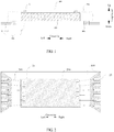
FIG. 1 is a schematic diagram of a longitudinal section of a sensor chip package assembly according to an embodiment of the present application; -
FIG. 2 is a schematic diagram of a cross section of a sensor chip package assembly according to an embodiment of the present application; -
FIG. 3 is a schematic diagram of a cross section of a sensor chip package assembly according to another embodiment of the present application; -
FIG. 4 is a schematic diagram of a cross section of a sensor chip package assembly according to yet another embodiment of the present application; -
FIG. 5 is a schematic diagram of a longitudinal section of a sensor chip package assembly according to another embodiment of the present application; -
FIG. 6 is a schematic diagram of a longitudinal section of a sensor chip package assembly according to yet another embodiment of the present application; -
FIG. 7 is a schematic diagram of change in a position of a pin according to an embodiment of the present application; -
FIG. 8 is a schematic diagram of a chip support portion according to an embodiment of the present application; -
FIG. 9a andFIG. 9b are respectively schematic diagrams of surface half-etching and stereoscopic surface half-etching of a metal bonding pad according to an embodiment of the present application; -
FIG. 10 is a schematic diagram of a laterally exposed metal bonding pad according to an embodiment of the present application; and -
FIG. 11 is a schematic diagram of a special-shaped structure of a packaging material cover according to an embodiment of the present application. - Embodiments of the present application will be described in detail below, and examples of the embodiments are shown in the drawings, in which identical or similar reference numbers denote identical or similar elements, or elements with identical or similar functions. The following embodiments described with reference to the drawings are exemplary and intended to be used to explain the present application, and may not be understood as limiting the present application.
- In the description of the present application, it should be understood that orientations or positional relationships indicated by terms such as "center", "longitudinal", "crosswise", "length", "width", "thickness", "up", "down", "front", "rear", "left", "right", "vertical", "horizontal", "top", "bottom", "inside", "outside", "clockwise", "anticlockwise", "axial direction", "radial direction" and "circumferential direction" are orientations or positional relationships shown based on the drawings, and the terms are merely for convenience of describing the present application and for simplifying the description, but for indicating or implying that an indicated apparatus or element must have a specific orientation, and must be constructed and operated in a specific orientation, which thus may not be understood as limiting the present application.
- Besides, terms "first" and "second" are for a descriptive purpose only, and may not be understood as indicating or implying relative importance, or implicitly indicating the quantity of indicated technical features. As such, features defined with the terms "first" and "second" may explicitly indicate or implicitly include at least one of the features. In the description of the present application, the meaning of "multiple" is at least two, for example, two, three, etc., unless explicitly and specifically defined otherwise.
- In the present application, unless explicitly specified and defined otherwise, terms such as "installation", "interconnection", "connection" and "fixation" should be understood broadly, for example, they may either be a fixed connection, or a detachable connection, or integrated; they may either be a mechanical connection, or an electric connection; and they may either be a direct connection, or an indirect connection through an intermediary, and they may be an internal connection between two elements or an interaction relationship between the two elements, unless explicitly defined otherwise. A person of ordinary skill in the art may understand specific meanings of the above terms in the present application according to specific conditions.
- In the present application, unless explicitly specified and defined otherwise, a first feature being "on" or "under" a second feature may be that the first feature and the second feature are in direct contact, or the first feature and the second feature are in indirect contact through an intermediary. In addition, the first feature being "on", "over" and "above" the second feature may be that the first feature is just above or diagonally above the second feature, or merely represents that a horizontal height of the first feature is higher than that of the second feature. The first feature being "under", "below" and "underneath" the second feature may be that the first feature is just below or diagonally below the second feature, or merely represents that the horizontal height of the first feature is lower than that of the second feature.
- According to one aspect of the present application, the present application provides a sensor chip package assembly. According to an embodiment of the present application, with reference to
FIG. 1 , the sensor chip package assembly includes: ametal substrate 100, asensor chip 200, anelectrical connection assembly 300 and apackaging material cover 400, where themetal substrate 100 has abonding pad region 11 and aplacement region 12, thebonding pad region 11 having a plurality ofmetal bonding pads 13; thesensor chip 200 is located on an upper surface of themetal substrate 100, and thesensor chip 200 has a plurality of sensorchip bonding pads 21; theelectrical connection assembly 300 electrically connecting ametal bonding pad 13 and a sensorchip bonding pad 21; and thepackaging material cover 400 covers themetal substrate 100, thesensor chip 200 and theelectrical connection assembly 300, and a lower surface of themetal substrate 100 is not covered by thepackaging material cover 400, where any two adjacentmetal bonding pads 13 are spaced in an insulated manner by thepackaging material cover 400. The inventor finds that, due to features of a short development period and lower cost of a metal substrate, a sensor chip package assembly with the metal substrate replacing a traditional PCB substrate, enables cost of producing the sensor chip package assembly to be saved significantly. Meanwhile, since a coefficient of thermal expansion of the metal substrate is fixed, it may effectively solve a problem that a conventional PCB substrate has large warpage, and may further improve efficiency of subsequent assembly significantly. Moreover, use of the metal substrate makes a direction of selecting resin as a packaging material more clear such that a product may avoid a lot of detours of repeated verification of injection molding, thus further reducing the cost of producing the sensor chip package assembly. In addition, since a plurality of metal bonding pads are independent from each other on the metal substrate, by adopting a metal substrate in a structure of the present application, it may realize independently transmitting a plurality of signals between a sensor chip and the metal substrate, thus dramatically reducing risk of interference among the plurality of signals. - According to an embodiment of the present application, the
bonding pad region 11 and theplacement region 12 on themetal substrate 100 may be two regions independent from each other on the metal substrate, that is, the two regions are not interconnected. - According to another embodiment of the present application, the metal substrate may either be a metal substrate on which a bonding pad region and a placement region are pre-disconnected from each other, or a metal substrate on which a bonding pad region and a placement region are pre-interconnected and subsequently separated from each other by etching. Particularly, no matter the metal substrate on which the bonding pad region and the placement region are pre-disconnected from each other is adopted or the metal substrate on which the bonding pad region and the placement region are pre-interconnected and subsequently separated from each other by etching is adopted, metal bonding pads in the bonding pad region may all be fixed finally with action of a packaging material cover so that a direct connection of a signal between a sensor chip and the metal substrate may be realized, thus effectively avoiding mutual interference of a plurality of signals.
- According to yet another embodiment of the present application, a specific type of the
metal substrate 100 is not particularly limited, and according to a specific embodiment of the present application, themetal substrate 100 may be a copper substrate. As such, since a copper substrate has a single component as compared with a traditional PCB substrate, by adopting the copper substrate, a coefficient of thermal expansion of the metal substrate is enabled to be relatively fixed, and it may effectively solve a problem that a conventional PCB substrate has large warpage, and may further improve the efficiency of subsequent assembly significantly. Moreover, use of the copper substrate makes a direction of selecting resin as a packaging material more clear than a metal substrate of another type such that a product may avoid a lot of detours of repeated verification of injection molding, thus further reducing the cost of producing the sensor chip package assembly. - A person skilled in the art may understand that a chip or a package assembly is fabricated as a whole strip, that is, respective die chips or package assemblies (hereinafter referred as "die") are connected, and are required to be cut into dies subsequently to continue producing modules. In other words, each kind of package design is a design based on a die, but production is carried out based on joining dies together to form a large board.
- For example, the sensor chip package assembly of the embodiments of the present application may be a die sensor chip package assembly after being cut, of which a package design is a design based on a die, but production is carried out based on a large board.
- According to yet another embodiment of the present application, a chip holding portion of the metal substrate may adopt a recessed design or a coplanar design, and a position of an output point of a metal bonding pad may be lifted by adopting the recessed design.
- The chip holding portion refers to a portion on the metal substrate where a chip is placed in a package assembly. The recessed design is that the portion is recessed, which makes the chip shift downward, and thus the position of the output point of the metal bonding pad, i.e., a position of a pin (pin), is lifted. In this way, after a plastic package is completed, there will be an insulation material (as shown in
FIG. 7 , black parts represent the insulation material) with a certain thickness under the pin, and thus a short circuit is difficult to occur. - It should be understood that the chip holding portion may also be non-recessed, i.e., adopting the coplanar design, which will not be limited in the present application.
- According to yet another embodiment of the present application, the chip support portion of the metal substrate may be placed at four corners thereof or be placed among metal bonding pads, or a support point thereof may be added or deleted as required.
- The chip support portion is a diepad (diepad) provided on the metal substrate for supporting a chip. As shown in
FIG. 8 , the chip support portion may either be placed at four corners of the metal substrate or be placed among the metal bonding pads. The chip support portion being placed among the metal bonding pads is more convenient to be cut. - According to yet another embodiment of the present application, the metal substrate may be a copper substrate or a substrate with tin, silver, etc. plated on a copper base material, and may also be another conductive material, and the present application is not limited to this.
- According to yet another embodiment of the present application, the metal substrate adopts half-etching or half-cutting after packaging among dies to realize insulation of different circuits so as to facilitate a latter strip process test, etc.
- Specifically, a package assembly is fabricated as a whole strip, and respective dies thereof are connected and cannot be tested, and thus it needs to be separated physically to realize electrical separation. The package assembly needs to be electrically separated, but cannot be cut off by a whole strip because the package assembly cannot be cut into any desired shape by a module factory according to a project requirement if it is cut off. The dies are insulated through electrical separation in a half-etching or half-cutting mode, thereby not disturbing a mutual test.
- According to yet another embodiment of the present application, the metal substrate may be a whole strip of substrate with pre-protected terminals, or a layer of metal substrate with coplanar pins formed through electroplating.
- Specifically, interconnection setting of the metal substrate may either be preset before an assembly is packaged, or be set after the assembly is packaged. A package manner adopted by a presetting may either be an advanced quad flat no-lead package (Advanced Quad Flat No-lead Package, aQFN), or be a molded interconnect system (molded interconnect system, MIS) package.
- According to yet another embodiment of the present application, a pin of the metal substrate may be a no-lead bonding pad and terminal, or a protruding pin of a J type, a P type and an N type.
- The pin of the metal substrate is connected to the metal bonding pad, and the pin may be package leads corresponding to various package types, for example, it may be a no-lead bonding pad, terminal, or a protruding pin of a J type, P type and N type. According to yet another embodiment of the present application, shapes of a plurality of metal bonding pads on the metal substrate may be different, which may be selected by a person skilled in the art according to actual needs. According to a specific embodiment of the present application, the plurality of metal bonding pads may be circular or polygonal, for example, as shown in
FIGS. 2-4 , the plurality of metal bonding pads may either be strip metal bonding pads in an identical shape and size, or be strip metal bonding pads in an identical shape and different lengths, or be circular metal bonding pads in an identical size, and specifically, a person skilled in the art may make a selection according to actual needs of signal transmission. It should be noted that a person skilled in the art may combine the metal bonding pads in the above three shapes according to actual needs. - According to yet another embodiment of the present application, a laterally exposed size of a metal bonding pad will be reduced between connected dies by adopting designs including surface half-etching, or stereoscopic surface half-etching, or hollowing, but the present application is not limited to this.
- Specifically, each kind of package design is a design based on a die, while production is carried out based on joining dies together to form a large board. Large board imposition needs to make an interconnection design among dies to reduce an interconnection area, thickness, size, etc. among the dies as much as possible so as to contribute to subsequent electrical separation, electro-static discharge (Electro-Static discharge, ESD), etc. Etching and hollowing may be designed for a whole leadframe (leadframe), where the hollowing design is that hollowness spreads all over an ordinary leadframe, the surface half-etching is as shown in
FIG. 9a , and the stereoscopic surface half-etching is as shown inFIG. 9b . - According to yet another embodiment of the present application, a specific type of the
sensor chip 200 is not particularly limited, which may be selected by a person skilled in the art according to actual needs. According to a specific embodiment of the present application, thesensor chip 200 may be a capacitive sensor chip. Specifically, the sensor chip has an integrated circuit, and when being powered on, the integrated circuit may generate a signal, and realize a function of a certain purpose. - According to yet another embodiment of the present application, the sensor
chip bonding pads 21 on thesensor chip 200 correspond to themetal bonding pads 13 one to one so that independent transmission of a plurality of signals between the sensor chip and the metal substrate may be realized, thus reducing mutual interference among the plurality of signals. - According to yet another embodiment of the present application, a specific type of the
electrical connection assembly 300 is not particularly limited, which may be selected by a person skilled in the art according to actual needs. According to a specific embodiment of the present application, theelectrical connection assembly 300 may be a bonding wire or a metal bump. According to a specific example of the present application, as shown inFIG. 5 , theelectrical connection assembly 300 is a bonding wire, and thesensor chip 200 is located on an upper surface of theplacement region 12 of themetal substrate 100, where the bonding wire electrically connects the sensor chip bonding pad and the metal bonding pad so that transmission of signal between the sensor chip and the metal substrate may be realized. According to another specific example of the present application, as shown inFIG. 6 , theelectrical connection assembly 300 is a metal bump, and thesensor chip 200 is located on themetal substrate 100, where thesensor chip 200 is fixed by the metal bump on themetal substrate 100, and the metal bump electrically connects the sensor chip bonding pad and the metal bonding pad so that transmission of the signal between the sensor chip and the metal substrate may be realized. - According to yet another embodiment of the present application, a specific type of the bonding wire is not particularly limited, which may be selected by a person skilled in the art according to actual needs. According to a specific embodiment of the present application, the bonding wire may be a gold wire, a copper wire, an aluminum wire, or an alloy wire. As such, since this type of wire has lower resistance, it may significantly improve stable transmission of the signal between the sensor chip and the metal substrate.
- According to yet another embodiment of the present application, a wire diameter of the bonding wire is not particularly limited, which may be selected by a person skilled in the art according to actual needs. According to a specific embodiment of the present application, a particle diameter of the bonding wire may be not less than 15 micrometers. The inventor finds that, if the wire diameter of the bonding wire is less than 15 micrometers, an obtained bonding wire is subject to lying on an edge of a chip due to less wire tension, thus resulting in a short circuit of the chip.
- According to yet another embodiment of the present application, a specific type of the metal bump is not particularly limited, which may be selected by a person skilled in the art according to actual needs. According to a specific embodiment of the present application, the metal bump may be a gold bump, a copper bump, or a tin bump. As such, stability of transmitting the signal between the sensor chip and the metal substrate may be further improved.
- According to yet another embodiment of the present application, a specific type of the
packaging material cover 400 is not particularly limited, which may be selected by a person skilled in the art according to actual needs. According to a specific embodiment of the present application, the packaging material cover may be an assembly formed by a material of which a dielectric constant is greater than 3. - According to a specific embodiment of the present application, the packaging material cover may be made of epoxy resin. The inventor finds that, this type of packaging material has good chemical stability, good thermal conductivity and a small coefficient of thermal expansion, and also possesses characteristics of better mechanical strength, ease in fabrication, a low price and ease in automatic production, and therefore selecting this type of packaging material may further improve stability and reliability of a sensor chip package assembly.
- According to yet another embodiment of the present application, a distance between the sensor chip and the metal bonding pad is not particularly limited, which may be selected by a person skilled in the art according to actual needs. According to a specific embodiment of the present application, the distance between the sensor chip and the metal bonding pad may be greater than 20 micrometers. The inventor finds that, technically, with regard to a manner of a bonding wire, the bonding wire needs igniting a ball, a wire diameter is greater than 15 micrometers, and a solder ball and a chip have thicknesses per se, of which a total thickness will be greater than 20 micrometers, the distance between the sensor chip and the metal bonding pad that is less than 20 micrometers will result in an insufficient remaining connection distance of a ball neck; and with regard to a manner of a metal bump, a height of the metal bump itself is usually higher than 20 micrometers. To sum up, if a distance between a sensor chip and a metal bonding pad is less than 20 micrometers, there will exist difficulty in a connection between the chip and the metal bonding pad.
- According to yet another embodiment of the present application, the packaging material cover may either completely cover an upper surface of the sensor chip, or merely cover the periphery of the sensor chip with the upper surface thereof being exposed, and a person skilled in the art may select a specific structure according to actual needs.
- According to yet another embodiment of the present application, a layer of another cover with good insulativity may be covered on the packaging material cover after die cutting is completed so as to enhance antistatic protection of a laterally exposed metal bonding pad.
- A package assembly is always manufactured as a whole strip, and is required to be cut into dies subsequently to continue producing modules. A material of the another cover with good insulativity may be an insulation material in a resin type, which will not be limited in the present application.
- A schematic diagram of the laterally exposed metal bonding pad is as shown in
FIG. 10 , where an upper surface thereof is functional (i.e., being related to a function of a chip) and needs to be protected using an insulation material, and thus static electricity cannot be discharged through the upper surface; and other surfaces is nonfunctional, and thus the static electricity may be introduced to the ground through another surface. The upper surface may be protected by covering the layer of another cover with good insulativity on the packaging material cover. - According to yet another embodiment of the present application, the another cover contains a metal particle of which a volume proportion may be less than 8%, and the metal particle is of a wrapped type or a non-wrapped type.
- Specifically, in order to maintain a minimum color difference with a metal casing, a metal particle (metal power) may be added into a cover. An ordinary metal particle is an ordinary crushed small particle. A particle of a wrapped type refers to a particle obtained by crushing a sandwich folded structure formed by plating a layer of metal film and a layer of resin on a resin film, and a purpose of adopting the particle is to reduce a conductive probability without reducing metal luster. With respect to the particle of the wrapped type, the previous ordinary particle is called a particle of a non-wrapped type.
- According to yet another embodiment of the present application, a specific area of the packaging material cover may be printed with a word, for example, product traceability information is marked by means of a laser or printing ink.
- For example, the specific area may be a gap region between the sensor chip and the metal bonding pad.
- According to yet another embodiment of the present application, the packaging material cover and the metal substrate adopt a fillet or chamfer design before being cut into dies, i.e., reserving a fillet or a chamfer, but the present application is not limited to this.
- For example, as shown in
FIG. 8 , in order to facilitate cutting a die assembly into a fillet or chamfer shape, the packaging material cover and the metal substrate may be reserved with a fillet or a chamfer thereon before being cut into dies. - According to yet another embodiment of the present application, the packaging material cover may be a stereoscopic special-shaped structure.
- Specifically, the stereoscopic special-shaped structure refers to that a surface is raised or recessed, and the surface may be raised or recessed partly or regionally.
- For example, as shown in
FIG. 11 , the left one is a traditional structure which is not special-shaped, and the right one is a special-shaped structure. - According to yet another embodiment of the present application, a color of the packaging material cover includes black, gray, etc., but it is not limited to this.
- According to yet another embodiment of the present application, the packaging material cover may be achieved by polishing a transfer mold (transfer mold) with thickened material spacing, or achieved using a thinner compression mold (compression mold) so as to facilitate reducing situation of an inner aperture and being not filled to the brim to a minimum.
- Generally, injection molding has situation of an aperture and being not filled to the brim on a micro level. Internal air is discharged through an air drain, sometimes an injection molding flow quickly blocks the air drain, and thus the air has no discharge path, which causes the situation of the aperture and being not filled to the brim. In this case, a flow direction of a molding flow cannot be controlled inside a mold, and the air drain may only be positioned at an edge, a corner and a bottom edge so as to avoid an influence on product appearance by overflow of the air drain.
- A packaging (plastic packaging) material is pressurized to change from a solid state to a liquid state, and similar to a mud-rock flow, it includes a large quantity of filling particles (like rocks in the mud-rock flow). If a reserved gap between a surface of a chip and a mold is too small, it will cause that these filling particles are jammed in a casing, and the molding flow cannot flow through, failing to fill the mold. However, if the reserved gap is very large, it will cause that a cover material on the surface of the chip is too thick, thus affecting penetrability of the chip. Therefore, polishing a mold after thickening it may not only solve a penetrability problem, but also solve a problem of defects such as being not filled to the brim. Besides, it may be achieved using a thinner compression mold, which will not be limited in the present application.
- According to yet another embodiment of the present application, a material filling particle of the packaging material cover should be as small as possible, and a typical value of a diameter thereof is less than or equal to 40um. Filling particles with good fluidity are dispersed uniformly, and not easy to aggregate to form partial concentration of large particles.
- According to yet another embodiment of the present application, a surface of the sensor chip contains a passivation layer, and a thickness of the passivation layer is more than 10 nanometers, and a color of the passivation layer may either be in black or another color, or transparent.
- According to yet another embodiment of the present application, a sensor chip may be interconnected with another chip through a wire in a through-silicon via, an edge chamfer or a backside bevel edge chamfer.
- For example, the another chip may be a control chip, a memory chip, etc. In the embodiment of the present application, the above manners are adopted to perform an interconnection so as to avoid using a bonding wire to perform the interconnection.
- According to yet another embodiment of the present application, the sensor chip may be a separate sensor chip, or another memory chip or a processor chip including the sensor chip, etc.
- To facilitate understanding, a method for producing the sensor chip package assembly of the embodiments of the present application will be described below in detail. The following takes an electrical connection member being a bonding wire and a metal substrate being a complete substrate as examples.
- Firstly, an adhesive is coated in a placement region of a metal substrate so as to form an adhesive layer in the placement region of the metal substrate. A person skilled in the art may select a type of an adopted adhesive and a thickness of the adhesive layer according to actual needs. Secondly, a sensor chip is placed on the adhesive layer so as to make the sensor chip fixed on an upper surface of the placement region of the metal substrate, and a bonding wire is adopted to realize electrically connecting a sensor chip bonding pad and a metal bonding pad. Then an obtained assembly is placed in a mold, an upper portion of the mold being higher than an upper surface of the sensor chip, and a liquid packaging material is filled into the mold. A person skilled in the art may adjust conditions such as a filling quantity, filling pressure, and a temperature of the liquid packaging material according to actual needs. Then an obtained chip assembly filled with the packaging material is solidified. Those skilled in the art may adjust conditions such as a solidification time, a solidification temperature and solidification pressure according to actual needs. Lastly, the metal substrate is etched along an edge of a bonding pad region so as to make the bonding pad region disconnected from the placement region, and a plurality of metal bonding pads are spaced from each other. Since a packaging material exists among the plurality of metal bonding pads, the above sensor chip package assembly may be obtained. When the bonding pad region is cut off, a separate metal bonding pad may be intact fixed by a packaging material cover without falling off so that security of using a package may be guaranteed.
- According to a second aspect of the present application, the present application provides an electronic device. According to an embodiment of the present application, the electronic device includes the above sensor chip package assembly. As such, by using the above sensor chip package assembly, a development period and raw material cost of the electronic device may be dramatically reduced, and stability of transmitting a signal inside the electronic device may be improved significantly at the same time. It should be noted that features and advantages described previously with regard to the sensor chip package assembly are also applicable to the electronic device, which will not be described redundantly herein.
- In the illustrations of the present description, descriptions given with reference to terms such as "an embodiment", "some embodiments", "an example", "a specific embodiment" or "some examples" means that a specific characteristic, structure, material or feature described with reference to the embodiment or example are included in at least one embodiment or example of the present application. In the present description, exemplary statements of the above terms are not required to direct at an identical embodiment or example. Furthermore, the described specific characteristic, structure, material or feature may be combined in a suitable manner in any one or more embodiments or examples. In addition, in a non-contradictory situation, a person skilled in the art may combine different embodiments or examples described in the present description and a characteristic of the different embodiments or examples.
- Although embodiments of the present application have been described and illustrated above, it may be understood that the above embodiments are exemplary and may not be understood as limiting the present application, and a person of ordinary skill in the art may make changes, modifications, substitutions and variations to the above embodiments within the scope of the present application.
Claims (32)
- A sensor chip package assembly, comprising:a metal substrate, the metal substrate having a bonding pad region and a placement region, and the bonding pad region having a plurality of metal bonding pads;a sensor chip, the sensor chip being located on an upper surface of the metal substrate, and the sensor chip having a plurality of sensor chip bonding pads;an electrical connection assembly, the electrical connection assembly electrically connecting a metal bonding pad and a sensor chip bonding pad; anda packaging material cover, the packaging material cover covering the metal substrate, the sensor chip and the electrical connection assembly, and a lower surface of the metal substrate being not covered by the packaging material cover, wherein any two adjacent metal bonding pads are spaced in an insulated manner by the packaging material cover.
- The sensor chip package assembly according to claim 1, wherein the electrical connection assembly is a bonding wire or a metal bump.
- The sensor chip package assembly according to claim 2, wherein the bonding wire is a gold wire, a copper wire, an aluminum wire, or an alloy wire.
- The sensor chip package assembly according to claim 2, wherein the metal bump is a gold bump, a copper bump, or a tin bump.
- The sensor chip package assembly according to any one of claims 1-4, wherein shapes of the plurality of metal bonding pads are different.
- The sensor chip package assembly according to any one of claims 1-5, wherein a shape of the metal bonding pad is circular or polygonal.
- The sensor chip package assembly according to any one of claims 1-6, wherein the metal bonding pad adopts a half-etching or a hollowing design.
- The sensor chip package assembly according to any one of claims 1-7, wherein the metal substrate is provided with a chip holding portion, the chip holding portion of the metal substrate adopting a recessed design or a coplanar design.
- The sensor chip package assembly according to any one of claims 1-8, wherein the metal substrate is provided with a chip support portion, the chip support portion of the metal substrate being placed at four corners of the metal substrate or being placed among the plurality of metal bonding pads.
- The sensor chip package assembly according to any one of claims 1-9, wherein the metal substrate is a copper substrate or a substrate with tin or silver plated on a copper base material.
- The sensor chip package assembly according to any one of claims 1-10, wherein the metal substrate adopts half-etching or half-cutting after packaging among dies to realize circuit insulation among different dies.
- The sensor chip package assembly according to any one of claims 1-11, wherein the metal substrate is a whole strip of substrate with pre-protected terminals, or a layer of metal substrate with coplanar pins formed through electroplating.
- The sensor chip package assembly according to any one of claims 1-12, wherein the metal substrate is provided with a pin, the pin of the metal substrate being a no-lead bonding pad or terminal, or a protruding pin of a J type, a P type or an N type.
- The sensor chip package assembly according to any one of claims 1-13, wherein a dielectric constant of the packaging material cover is greater than 3.
- The sensor chip package assembly according to any one of claims 1-14, wherein the sensor chip package assembly further comprises another cover on the packaging material cover.
- The sensor chip package assembly according to claim 15, wherein another cover comprises a metal particle.
- The sensor chip package assembly according to claim 16, wherein a volume proportion of the metal particle in the another cover is less than 8%.
- The sensor chip package assembly according to claim 16 or 17, wherein the metal particle is of a wrapped type or a non-wrapped type.
- The sensor chip package assembly according to any one of claims 1-18, wherein product traceability information is marked in a specific area of the packaging material cover.
- The sensor chip package assembly according to any one of claims 1-19, wherein the packaging material cover and the metal substrate adopt a fillet or chamfer design before being cut into dies.
- The sensor chip package assembly according to any one of claims 1-20, wherein the packaging material cover is a stereoscopic special-shaped structure.
- The sensor chip package assembly according to any one of claims 1-21, wherein a color of the packaging material cover is black or gray.
- The sensor chip package assembly according to any one of claims 1-22, wherein the packaging material cover is achieved through a transfer mold with thickened material spacing, or is achieved using a thinner compression mold.
- The sensor chip package assembly according to any one of claims 1-23, wherein a diameter of a material filling particle of the packaging material cover is less than or equal to 40 um.
- The sensor chip package assembly according to any one of claims 1-24, wherein a distance between the sensor chip and the metal bonding pad is greater than 20 micrometers.
- The sensor chip package assembly according to any one of claims 1-25, wherein a surface of the sensor chip comprises a passivation layer.
- The sensor chip package assembly according to claim 26, wherein a thickness of the passivation layer is more than 10 nanometers.
- The sensor chip package assembly according to claim 26 or 27, wherein a color of the passivation layer is black or transparent.
- The sensor chip package assembly according to any one of claims 1-28, wherein the sensor chip is interconnected with another chip through a wire in a through-silicon via, an edge chamfer or a backside bevel edge chamfer.
- The sensor chip package assembly according to any one of claims 1-29, wherein the sensor chip is a memory chip or a processor chip including the sensor chip.
- An electronic device, comprising the sensor chip package assembly according to any one of claims 1-30.
- A method for producing the sensor chip package assembly according to any one of claims 1-30, comprising:coating an adhesive in a placement region of a metal substrate so as to form an adhesive layer in the placement region of the metal substrate;placing a sensor chip on the adhesive layer so as to make the sensor chip fixed on an upper surface of the placement region of the metal substrate;electrically connecting a sensor chip bonding pad with a metal bonding pad;placing an obtained assembly in a mold, an upper portion of the mold being higher than an upper surface of the sensor chip, and filling a liquid packaging material into the mold;solidifying an obtained chip assembly filled with the packaging material; andetching the metal substrate along an edge of a bonding pad region so as to make the bonding pad region disconnected from the placement region.
Applications Claiming Priority (2)
| Application Number | Priority Date | Filing Date | Title |
|---|---|---|---|
| CN201520701432.5U CN204991696U (en) | 2015-09-11 | 2015-09-11 | Sensing chip package subassembly and electronic equipment who has this sensing chip package subassembly |
| PCT/CN2016/098161 WO2017041689A1 (en) | 2015-09-11 | 2016-09-06 | Sensing chip encapsulation component and electronic device with same |
Publications (2)
| Publication Number | Publication Date |
|---|---|
| EP3214648A1 true EP3214648A1 (en) | 2017-09-06 |
| EP3214648A4 EP3214648A4 (en) | 2018-04-04 |
Family
ID=55126034
Family Applications (1)
| Application Number | Title | Priority Date | Filing Date |
|---|---|---|---|
| EP16843627.7A Ceased EP3214648A4 (en) | 2015-09-11 | 2016-09-06 | Sensing chip encapsulation component and electronic device with same |
Country Status (5)
| Country | Link |
|---|---|
| US (1) | US10121750B2 (en) |
| EP (1) | EP3214648A4 (en) |
| KR (1) | KR101964763B1 (en) |
| CN (1) | CN204991696U (en) |
| WO (1) | WO2017041689A1 (en) |
Cited By (1)
| Publication number | Priority date | Publication date | Assignee | Title |
|---|---|---|---|---|
| CN113199103A (en) * | 2021-06-11 | 2021-08-03 | 哈尔滨工业大学 | Electromagnetic induction quick connection method suitable for high-power electronic device or assembly |
Families Citing this family (13)
| Publication number | Priority date | Publication date | Assignee | Title |
|---|---|---|---|---|
| CN204991696U (en) | 2015-09-11 | 2016-01-20 | 深圳市汇顶科技股份有限公司 | Sensing chip package subassembly and electronic equipment who has this sensing chip package subassembly |
| CN106463492B (en) * | 2016-09-06 | 2019-12-10 | 深圳市汇顶科技股份有限公司 | Sensing chip packaging assembly and electronic equipment with same |
| KR101853296B1 (en) * | 2016-09-13 | 2018-04-30 | (주)포인트엔지니어링 | Micro sensor package and manufacturing method of micro sensor package |
| WO2018082087A1 (en) * | 2016-11-07 | 2018-05-11 | 深圳市汇顶科技股份有限公司 | Fingerprint recognition module and fingerprint recognition chip packaging structure |
| EP3422405B1 (en) * | 2017-01-22 | 2024-12-18 | Shenzhen Goodix Technology Co., Ltd. | Fingerprint sensor chip package |
| US10734304B2 (en) * | 2018-11-16 | 2020-08-04 | Texas Instruments Incorporated | Plating for thermal management |
| TWI764256B (en) * | 2020-08-28 | 2022-05-11 | 朋程科技股份有限公司 | Intelligent power module packaging structure |
| CN114209297A (en) * | 2021-11-24 | 2022-03-22 | 广东紫文星电子科技有限公司 | Module with heart rate detection and fingerprint identification functions and authentication method |
| CN117119736A (en) * | 2022-05-16 | 2023-11-24 | 群创光电股份有限公司 | electronic device |
| CN114873557A (en) * | 2022-05-31 | 2022-08-09 | 广州市意芯微电子有限公司 | Interconnection packaging method for micro-electromechanical sensor |
| CN115417370A (en) * | 2022-09-15 | 2022-12-02 | 西安秦铂瑞科技有限公司 | Packaging structure and packaging method of pressure sensor chip |
| CN119137732A (en) * | 2022-10-13 | 2024-12-13 | 深圳华大生命科学研究院 | Sensor chip packaging structure, method, PCB substrate and microfluidic detection device |
| CN121113127A (en) * | 2025-11-13 | 2025-12-12 | 河北美泰电子科技有限公司 | A packaging structure for an inertial sensor |
Family Cites Families (30)
| Publication number | Priority date | Publication date | Assignee | Title |
|---|---|---|---|---|
| JPS5544763A (en) * | 1978-09-25 | 1980-03-29 | Nec Kyushu Ltd | Semiconductor |
| JP3686287B2 (en) * | 1999-07-14 | 2005-08-24 | 株式会社ルネサステクノロジ | Manufacturing method of semiconductor device |
| US6777265B2 (en) * | 2002-04-29 | 2004-08-17 | Advanced Interconnect Technologies Limited | Partially patterned lead frames and methods of making and using the same in semiconductor packaging |
| US8236612B2 (en) | 2002-04-29 | 2012-08-07 | Unisem (Mauritius) Holdings Limited | Partially patterned lead frames and methods of making and using the same in semiconductor packaging |
| JP2005026466A (en) | 2003-07-02 | 2005-01-27 | Renesas Technology Corp | Semiconductor device and lead frame |
| JP4345685B2 (en) * | 2005-02-22 | 2009-10-14 | ヤマハ株式会社 | Physical quantity sensor, lead frame used therefor, and lead frame manufacturing method |
| US20060185452A1 (en) | 2005-02-22 | 2006-08-24 | Yamaha Corporation | Lead frame, sensor including lead frame, resin composition to be used for resin mold in the sensor, and sensor including the resin mold |
| JP2007294637A (en) * | 2006-04-25 | 2007-11-08 | Denso Corp | Manufacturing method of semiconductor device |
| WO2008057770A2 (en) * | 2006-10-27 | 2008-05-15 | Unisem (Mauritius) Holdings Limited | Partially patterned lead frames and methods of making and using the same in semiconductor packaging |
| US7816772B2 (en) * | 2007-03-29 | 2010-10-19 | Allegro Microsystems, Inc. | Methods and apparatus for multi-stage molding of integrated circuit package |
| TW201013881A (en) * | 2008-09-10 | 2010-04-01 | Renesas Tech Corp | Semiconductor device and method for manufacturing same |
| US9235747B2 (en) * | 2008-11-27 | 2016-01-12 | Apple Inc. | Integrated leadframe and bezel structure and device formed from same |
| DE102008054735A1 (en) * | 2008-12-16 | 2010-06-17 | Robert Bosch Gmbh | Leadless package housing |
| US7858443B2 (en) * | 2009-03-09 | 2010-12-28 | Utac Hong Kong Limited | Leadless integrated circuit package having standoff contacts and die attach pad |
| US8324602B2 (en) * | 2009-04-14 | 2012-12-04 | Intersil Americas Inc. | Optical sensors that reduce specular reflections |
| US9029999B2 (en) * | 2011-11-23 | 2015-05-12 | Freescale Semiconductor, Inc. | Semiconductor sensor device with footed lid |
| KR101357588B1 (en) * | 2011-12-22 | 2014-02-04 | 엘지이노텍 주식회사 | Leadless lead frame, semiconductor chip package using thereof and manufacturing method thereof |
| JP6195695B2 (en) * | 2012-01-24 | 2017-09-13 | 大日本印刷株式会社 | Resin-sealed semiconductor device, lead frame, wiring board with semiconductor device, and method for manufacturing wiring board with semiconductor device |
| JP5953626B2 (en) * | 2012-02-15 | 2016-07-20 | セイコーインスツル株式会社 | Photodetection device and method for manufacturing photodetection device |
| JP2013207213A (en) * | 2012-03-29 | 2013-10-07 | Tdk Corp | Electronic component module and manufacturing method thereof |
| US9147628B2 (en) * | 2012-06-27 | 2015-09-29 | Infineon Technoloiges Austria AG | Package-in-packages and methods of formation thereof |
| KR101548158B1 (en) * | 2012-09-07 | 2015-08-28 | 제일모직 주식회사 | Article and manufacturing method of article |
| US9580302B2 (en) * | 2013-03-15 | 2017-02-28 | Versana Micro Inc. | Cell phone having a monolithically integrated multi-sensor device on a semiconductor substrate and method therefor |
| US9368423B2 (en) * | 2013-06-28 | 2016-06-14 | STATS ChipPAC Pte. Ltd. | Semiconductor device and method of using substrate with conductive posts and protective layers to form embedded sensor die package |
| US20150054099A1 (en) * | 2013-08-25 | 2015-02-26 | Kai Yun Yow | Pressure sensor device and assembly method |
| JP6607429B2 (en) * | 2014-01-22 | 2019-11-20 | 大日本印刷株式会社 | Lead frame and manufacturing method thereof, and semiconductor device and manufacturing method thereof |
| TWI559463B (en) | 2014-10-31 | 2016-11-21 | 矽品精密工業股份有限公司 | Package structure and its manufacturing method |
| TWI570857B (en) | 2014-12-10 | 2017-02-11 | 矽品精密工業股份有限公司 | Package structure and its manufacturing method |
| CN205428898U (en) | 2015-08-28 | 2016-08-03 | 深圳市汇顶科技股份有限公司 | Packaging structure of sensing chip and protection architecture on surface thereof |
| CN204991696U (en) * | 2015-09-11 | 2016-01-20 | 深圳市汇顶科技股份有限公司 | Sensing chip package subassembly and electronic equipment who has this sensing chip package subassembly |
-
2015
- 2015-09-11 CN CN201520701432.5U patent/CN204991696U/en not_active Expired - Fee Related
-
2016
- 2016-09-06 EP EP16843627.7A patent/EP3214648A4/en not_active Ceased
- 2016-09-06 WO PCT/CN2016/098161 patent/WO2017041689A1/en not_active Ceased
- 2016-09-06 KR KR1020177015547A patent/KR101964763B1/en not_active Expired - Fee Related
-
2017
- 2017-06-01 US US15/611,766 patent/US10121750B2/en active Active
Cited By (1)
| Publication number | Priority date | Publication date | Assignee | Title |
|---|---|---|---|---|
| CN113199103A (en) * | 2021-06-11 | 2021-08-03 | 哈尔滨工业大学 | Electromagnetic induction quick connection method suitable for high-power electronic device or assembly |
Also Published As
| Publication number | Publication date |
|---|---|
| KR20170084174A (en) | 2017-07-19 |
| EP3214648A4 (en) | 2018-04-04 |
| KR101964763B1 (en) | 2019-08-07 |
| WO2017041689A1 (en) | 2017-03-16 |
| CN204991696U (en) | 2016-01-20 |
| US20170271278A1 (en) | 2017-09-21 |
| US10121750B2 (en) | 2018-11-06 |
Similar Documents
| Publication | Publication Date | Title |
|---|---|---|
| US10121750B2 (en) | Sensor chip package assembly and electronic device having sensor chip package assembly | |
| US6967125B2 (en) | Quad flat no lead (QFN) grid array package, method of making and memory module and computer system including same | |
| US7112875B1 (en) | Secure digital memory card using land grid array structure | |
| US9240393B2 (en) | High yield semiconductor device | |
| US6764879B2 (en) | Semiconductor wafer, semiconductor device, and method for manufacturing the same | |
| US8508048B2 (en) | Semiconductor device utilizing a package on package structure and manufacturing method thereof | |
| US7378301B2 (en) | Method for molding a small form factor digital memory card | |
| US8791556B2 (en) | Integrated circuit packaging system with routable circuitry and method of manufacture thereof | |
| US20070278701A1 (en) | Semiconductor package and method for fabricating the same | |
| US11139233B2 (en) | Cavity wall structure for semiconductor packaging | |
| US7495255B2 (en) | Test pads on flash memory cards | |
| CN111554652B (en) | Conductive trace design for smart cards | |
| CN211088270U (en) | Chip packaging structure and optical sensor | |
| US6160311A (en) | Enhanced heat dissipating chip scale package method and devices | |
| CN106463492B (en) | Sensing chip packaging assembly and electronic equipment with same | |
| CN105990299A (en) | BGA (Ball Grid Array) packaging structure and preparation method thereof | |
| US8022516B2 (en) | Metal leadframe package with secure feature | |
| CN107731694A (en) | A kind of assemble method of bio-identification module, bio-identification module and mobile terminal | |
| CN100452331C (en) | Bare chip building block packaging method | |
| US9076737B2 (en) | Integrated circuit packaging system with bumps and method of manufacture thereof | |
| CN119786446A (en) | Electronic package assembly and method of forming an electronic package assembly |
Legal Events
| Date | Code | Title | Description |
|---|---|---|---|
| STAA | Information on the status of an ep patent application or granted ep patent |
Free format text: STATUS: THE INTERNATIONAL PUBLICATION HAS BEEN MADE |
|
| PUAI | Public reference made under article 153(3) epc to a published international application that has entered the european phase |
Free format text: ORIGINAL CODE: 0009012 |
|
| STAA | Information on the status of an ep patent application or granted ep patent |
Free format text: STATUS: REQUEST FOR EXAMINATION WAS MADE |
|
| 17P | Request for examination filed |
Effective date: 20170518 |
|
| AK | Designated contracting states |
Kind code of ref document: A1 Designated state(s): AL AT BE BG CH CY CZ DE DK EE ES FI FR GB GR HR HU IE IS IT LI LT LU LV MC MK MT NL NO PL PT RO RS SE SI SK SM TR |
|
| AX | Request for extension of the european patent |
Extension state: BA ME |
|
| A4 | Supplementary search report drawn up and despatched |
Effective date: 20180306 |
|
| RIC1 | Information provided on ipc code assigned before grant |
Ipc: G01D 5/12 20060101ALI20180226BHEP Ipc: H01L 23/495 20060101AFI20180226BHEP Ipc: H01L 23/488 20060101ALI20180226BHEP Ipc: H01L 23/31 20060101ALI20180226BHEP Ipc: H01L 21/56 20060101ALI20180226BHEP Ipc: H01L 21/48 20060101ALI20180226BHEP |
|
| DAV | Request for validation of the european patent (deleted) | ||
| DAX | Request for extension of the european patent (deleted) | ||
| STAA | Information on the status of an ep patent application or granted ep patent |
Free format text: STATUS: EXAMINATION IS IN PROGRESS |
|
| 17Q | First examination report despatched |
Effective date: 20190225 |
|
| REG | Reference to a national code |
Ref country code: DE Ref legal event code: R003 |
|
| STAA | Information on the status of an ep patent application or granted ep patent |
Free format text: STATUS: THE APPLICATION HAS BEEN REFUSED |
|
| 18R | Application refused |
Effective date: 20201030 |