EP3213348B1 - Memristors with oxide switching layers - Google Patents
Memristors with oxide switching layers Download PDFInfo
- Publication number
- EP3213348B1 EP3213348B1 EP14903430.8A EP14903430A EP3213348B1 EP 3213348 B1 EP3213348 B1 EP 3213348B1 EP 14903430 A EP14903430 A EP 14903430A EP 3213348 B1 EP3213348 B1 EP 3213348B1
- Authority
- EP
- European Patent Office
- Prior art keywords
- oxide
- conductive material
- layer
- conductive
- conductive layer
- Prior art date
- Legal status (The legal status is an assumption and is not a legal conclusion. Google has not performed a legal analysis and makes no representation as to the accuracy of the status listed.)
- Not-in-force
Links
- 239000004020 conductor Substances 0.000 claims description 79
- 230000015654 memory Effects 0.000 claims description 26
- 238000000034 method Methods 0.000 claims description 16
- 230000001590 oxidative effect Effects 0.000 claims description 9
- 229910052782 aluminium Inorganic materials 0.000 claims description 8
- 229910052802 copper Inorganic materials 0.000 claims description 8
- 239000010949 copper Substances 0.000 claims description 8
- 238000004519 manufacturing process Methods 0.000 claims description 8
- 229910052710 silicon Inorganic materials 0.000 claims description 7
- VYPSYNLAJGMNEJ-UHFFFAOYSA-N Silicium dioxide Chemical compound O=[Si]=O VYPSYNLAJGMNEJ-UHFFFAOYSA-N 0.000 claims description 6
- 239000010703 silicon Substances 0.000 claims description 6
- 229910052814 silicon oxide Inorganic materials 0.000 claims description 6
- RYGMFSIKBFXOCR-UHFFFAOYSA-N Copper Chemical compound [Cu] RYGMFSIKBFXOCR-UHFFFAOYSA-N 0.000 claims description 5
- XAGFODPZIPBFFR-UHFFFAOYSA-N aluminium Chemical compound [Al] XAGFODPZIPBFFR-UHFFFAOYSA-N 0.000 claims description 5
- TWNQGVIAIRXVLR-UHFFFAOYSA-N oxo(oxoalumanyloxy)alumane Chemical compound O=[Al]O[Al]=O TWNQGVIAIRXVLR-UHFFFAOYSA-N 0.000 claims description 5
- QPLDLSVMHZLSFG-UHFFFAOYSA-N Copper oxide Chemical compound [Cu]=O QPLDLSVMHZLSFG-UHFFFAOYSA-N 0.000 claims description 4
- 239000005751 Copper oxide Substances 0.000 claims description 4
- 229910000431 copper oxide Inorganic materials 0.000 claims description 4
- 239000000463 material Substances 0.000 description 31
- 230000003647 oxidation Effects 0.000 description 8
- 238000007254 oxidation reaction Methods 0.000 description 8
- 239000000203 mixture Substances 0.000 description 5
- 229910017107 AlOx Inorganic materials 0.000 description 3
- XUIMIQQOPSSXEZ-UHFFFAOYSA-N Silicon Chemical compound [Si] XUIMIQQOPSSXEZ-UHFFFAOYSA-N 0.000 description 3
- 238000009792 diffusion process Methods 0.000 description 3
- 230000009286 beneficial effect Effects 0.000 description 2
- 238000012512 characterization method Methods 0.000 description 2
- 238000010586 diagram Methods 0.000 description 2
- 230000005611 electricity Effects 0.000 description 2
- 229910052735 hafnium Inorganic materials 0.000 description 2
- 229910052750 molybdenum Inorganic materials 0.000 description 2
- 229910052759 nickel Inorganic materials 0.000 description 2
- 229910052758 niobium Inorganic materials 0.000 description 2
- 229910052697 platinum Inorganic materials 0.000 description 2
- 239000000758 substrate Substances 0.000 description 2
- 229910052715 tantalum Inorganic materials 0.000 description 2
- 229910052719 titanium Inorganic materials 0.000 description 2
- 229910052721 tungsten Inorganic materials 0.000 description 2
- 229910052726 zirconium Inorganic materials 0.000 description 2
- 229910052692 Dysprosium Inorganic materials 0.000 description 1
- 229910052691 Erbium Inorganic materials 0.000 description 1
- 229910052688 Gadolinium Inorganic materials 0.000 description 1
- 229910052689 Holmium Inorganic materials 0.000 description 1
- 229910052765 Lutetium Inorganic materials 0.000 description 1
- 229910015345 MOn Inorganic materials 0.000 description 1
- 229910019794 NbN Inorganic materials 0.000 description 1
- 229910020044 NbSi2 Inorganic materials 0.000 description 1
- 229910052772 Samarium Inorganic materials 0.000 description 1
- 229910004479 Ta2N Inorganic materials 0.000 description 1
- 229910004166 TaN Inorganic materials 0.000 description 1
- 229910004217 TaSi2 Inorganic materials 0.000 description 1
- 229910009871 Ti5Si3 Inorganic materials 0.000 description 1
- 229910008484 TiSi Inorganic materials 0.000 description 1
- 229910008479 TiSi2 Inorganic materials 0.000 description 1
- ATJFFYVFTNAWJD-UHFFFAOYSA-N Tin Chemical compound [Sn] ATJFFYVFTNAWJD-UHFFFAOYSA-N 0.000 description 1
- 229910008814 WSi2 Inorganic materials 0.000 description 1
- 229910052769 Ytterbium Inorganic materials 0.000 description 1
- 229910045601 alloy Inorganic materials 0.000 description 1
- 239000000956 alloy Substances 0.000 description 1
- 238000003491 array Methods 0.000 description 1
- 238000000429 assembly Methods 0.000 description 1
- 230000000712 assembly Effects 0.000 description 1
- 238000000231 atomic layer deposition Methods 0.000 description 1
- QVGXLLKOCUKJST-UHFFFAOYSA-N atomic oxygen Chemical compound [O] QVGXLLKOCUKJST-UHFFFAOYSA-N 0.000 description 1
- 230000006399 behavior Effects 0.000 description 1
- 230000015572 biosynthetic process Effects 0.000 description 1
- DFJQEGUNXWZVAH-UHFFFAOYSA-N bis($l^{2}-silanylidene)titanium Chemical compound [Si]=[Ti]=[Si] DFJQEGUNXWZVAH-UHFFFAOYSA-N 0.000 description 1
- 229910052791 calcium Inorganic materials 0.000 description 1
- 238000005229 chemical vapour deposition Methods 0.000 description 1
- 229910052804 chromium Inorganic materials 0.000 description 1
- 238000000151 deposition Methods 0.000 description 1
- 230000000694 effects Effects 0.000 description 1
- 238000005516 engineering process Methods 0.000 description 1
- 238000001704 evaporation Methods 0.000 description 1
- 230000008020 evaporation Effects 0.000 description 1
- 229910052733 gallium Inorganic materials 0.000 description 1
- 229910052737 gold Inorganic materials 0.000 description 1
- 238000003384 imaging method Methods 0.000 description 1
- 238000007735 ion beam assisted deposition Methods 0.000 description 1
- 229910052742 iron Inorganic materials 0.000 description 1
- 229910052749 magnesium Inorganic materials 0.000 description 1
- 229910052748 manganese Inorganic materials 0.000 description 1
- 229910052751 metal Inorganic materials 0.000 description 1
- 239000002184 metal Substances 0.000 description 1
- 150000002739 metals Chemical class 0.000 description 1
- 229910052760 oxygen Inorganic materials 0.000 description 1
- 239000001301 oxygen Substances 0.000 description 1
- 229910052763 palladium Inorganic materials 0.000 description 1
- 230000002085 persistent effect Effects 0.000 description 1
- 238000005240 physical vapour deposition Methods 0.000 description 1
- 229910021420 polycrystalline silicon Inorganic materials 0.000 description 1
- 239000004065 semiconductor Substances 0.000 description 1
- 229910052709 silver Inorganic materials 0.000 description 1
- 239000007787 solid Substances 0.000 description 1
- 238000004544 sputter deposition Methods 0.000 description 1
- 238000003860 storage Methods 0.000 description 1
- 229910052712 strontium Inorganic materials 0.000 description 1
- 230000001360 synchronised effect Effects 0.000 description 1
- 229910052718 tin Inorganic materials 0.000 description 1
- 229910052720 vanadium Inorganic materials 0.000 description 1
- 229910052727 yttrium Inorganic materials 0.000 description 1
- 229910052725 zinc Inorganic materials 0.000 description 1
Images


Classifications
-
- B—PERFORMING OPERATIONS; TRANSPORTING
- B41—PRINTING; LINING MACHINES; TYPEWRITERS; STAMPS
- B41J—TYPEWRITERS; SELECTIVE PRINTING MECHANISMS, i.e. MECHANISMS PRINTING OTHERWISE THAN FROM A FORME; CORRECTION OF TYPOGRAPHICAL ERRORS
- B41J2/00—Typewriters or selective printing mechanisms characterised by the printing or marking process for which they are designed
- B41J2/005—Typewriters or selective printing mechanisms characterised by the printing or marking process for which they are designed characterised by bringing liquid or particles selectively into contact with a printing material
- B41J2/01—Ink jet
- B41J2/17—Ink jet characterised by ink handling
- B41J2/175—Ink supply systems ; Circuit parts therefor
- B41J2/17503—Ink cartridges
- B41J2/17526—Electrical contacts to the cartridge
- B41J2/1753—Details of contacts on the cartridge, e.g. protection of contacts
-
- B—PERFORMING OPERATIONS; TRANSPORTING
- B41—PRINTING; LINING MACHINES; TYPEWRITERS; STAMPS
- B41J—TYPEWRITERS; SELECTIVE PRINTING MECHANISMS, i.e. MECHANISMS PRINTING OTHERWISE THAN FROM A FORME; CORRECTION OF TYPOGRAPHICAL ERRORS
- B41J2/00—Typewriters or selective printing mechanisms characterised by the printing or marking process for which they are designed
- B41J2/005—Typewriters or selective printing mechanisms characterised by the printing or marking process for which they are designed characterised by bringing liquid or particles selectively into contact with a printing material
- B41J2/01—Ink jet
- B41J2/17—Ink jet characterised by ink handling
- B41J2/175—Ink supply systems ; Circuit parts therefor
- B41J2/17503—Ink cartridges
- B41J2/17543—Cartridge presence detection or type identification
- B41J2/17546—Cartridge presence detection or type identification electronically
-
- H—ELECTRICITY
- H10—SEMICONDUCTOR DEVICES; ELECTRIC SOLID-STATE DEVICES NOT OTHERWISE PROVIDED FOR
- H10N—ELECTRIC SOLID-STATE DEVICES NOT OTHERWISE PROVIDED FOR
- H10N70/00—Solid-state devices having no potential barriers, and specially adapted for rectifying, amplifying, oscillating or switching
- H10N70/011—Manufacture or treatment of multistable switching devices
- H10N70/021—Formation of switching materials, e.g. deposition of layers
- H10N70/028—Formation of switching materials, e.g. deposition of layers by conversion of electrode material, e.g. oxidation
-
- H—ELECTRICITY
- H10—SEMICONDUCTOR DEVICES; ELECTRIC SOLID-STATE DEVICES NOT OTHERWISE PROVIDED FOR
- H10N—ELECTRIC SOLID-STATE DEVICES NOT OTHERWISE PROVIDED FOR
- H10N70/00—Solid-state devices having no potential barriers, and specially adapted for rectifying, amplifying, oscillating or switching
- H10N70/20—Multistable switching devices, e.g. memristors
-
- H—ELECTRICITY
- H10—SEMICONDUCTOR DEVICES; ELECTRIC SOLID-STATE DEVICES NOT OTHERWISE PROVIDED FOR
- H10N—ELECTRIC SOLID-STATE DEVICES NOT OTHERWISE PROVIDED FOR
- H10N70/00—Solid-state devices having no potential barriers, and specially adapted for rectifying, amplifying, oscillating or switching
- H10N70/801—Constructional details of multistable switching devices
- H10N70/821—Device geometry
- H10N70/826—Device geometry adapted for essentially vertical current flow, e.g. sandwich or pillar type devices
-
- H—ELECTRICITY
- H10—SEMICONDUCTOR DEVICES; ELECTRIC SOLID-STATE DEVICES NOT OTHERWISE PROVIDED FOR
- H10N—ELECTRIC SOLID-STATE DEVICES NOT OTHERWISE PROVIDED FOR
- H10N70/00—Solid-state devices having no potential barriers, and specially adapted for rectifying, amplifying, oscillating or switching
- H10N70/801—Constructional details of multistable switching devices
- H10N70/841—Electrodes
-
- H—ELECTRICITY
- H10—SEMICONDUCTOR DEVICES; ELECTRIC SOLID-STATE DEVICES NOT OTHERWISE PROVIDED FOR
- H10N—ELECTRIC SOLID-STATE DEVICES NOT OTHERWISE PROVIDED FOR
- H10N70/00—Solid-state devices having no potential barriers, and specially adapted for rectifying, amplifying, oscillating or switching
- H10N70/801—Constructional details of multistable switching devices
- H10N70/881—Switching materials
- H10N70/883—Oxides or nitrides
- H10N70/8833—Binary metal oxides, e.g. TaOx
Definitions
- Printers can have printheads capable of depositing ink on a substrate.
- Printheads can include devices to store data.
- Memristors are devices that can be programmed to different resistive states by applying a programming energy, such as a voltage. After programming, the state of the memristor can be read and remains stable over a specified time period. Thus, memristors can be used to store digital data. For example, a high resistance state can represent a digital "0" and a low resistance state can represent a digital "1.”
- Large crossbar arrays of memristive elements can be used in a variety of applications, including non-volatile memory and other applications.
- Imaging devices may include printheads, which may have memory devices to store data.
- memory devices There are many different types of memory including volatile and non-volatile memory.
- Volatile memory can require power to maintain its data and includes random-access memory (RAM), dynamic random access memory (DRAM), and synchronous dynamic random access memory (SDRAM), among others.
- RAM random-access memory
- DRAM dynamic random access memory
- SDRAM synchronous dynamic random access memory
- Non-volatile memory can provide persistent data by retaining stored data when not powered and can include flash memory, read only memory (ROM), Electrically Erasable Programmable ROM (EEPROM), Erasable Programmable ROM (EPROM), and resistance variable memory such as phase change random access memory (PCRAM), resistive random access memory (RRAM), and magnetoresistive random access memory (MRAM), among others.
- EPROM has been incorporated into some printheads. However, with an increase in counterfeiting activity, more secure authentication and anti-counterfeit tools having a greater storage capacity are sought. Furthermore, as new technologies are
- Memristors have been proposed to be used in printheads. Memristors are devices that may be used as components in a wide range of electronic circuits, such as memories, switches, radio frequency circuits, and logic circuits and systems. In a memory structure, a crossbar array of memory devices having memristors may be used. When used as a basis for memory devices, memristors may be used to store bits of information, 1 or 0. The resistance of a memristor may be changed by applying an electrical stimulus, such as a voltage or a current, through the memristor.
- an electrical stimulus such as a voltage or a current
- At least one channel may be formed that is capable of being switched between two states-one in which the channel forms an electrically conductive path ("ON") and one in which the channel forms a less conductive path (“OFF").
- conductive paths represent "OFF” and less conductive paths represent "ON”.
- current proposed solutions present certain challenges, including inconsistent switching behavior and undesirable electrical conductivity in some implementations.
- a memristor with an oxide switching layer has a first conductive layer with a first conductive material and a second conductive material, a switching layer with a first oxide having the first conductive material and a second oxide having the second conductive material, and a second conductive layer as defined by claim 1.
- the presence of the second oxide in the switching layer alters the electrical properties of the switching layer to more desirable levels.
- the first oxide and the second oxide are formed by oxidizing the materials of the first conductive layer as defined by claim 4, which allows an effective and efficient mechanism to introduce two oxides in a single switching layer.
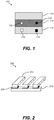
- FIG. 1 depicts an example memristor 100 with an oxide switching layer 120.
- Memristor 100 may have a first conductive layer 110, switching layer 120, and a second conductive layer 130.
- First conductive layer 110 may have a first conductive material 112 and a second conductive material 114.
- Switching layer 120 may be coupled to first conductive layer 110 and may include a first oxide 122 having first conductive material 112 and a second oxide 124 having second conductive material 114.
- Second conductive layer 130 may be coupled to switching layer 120.
- Memristor 100 may be an electrical device or component that has a resistance that changes with an applied electrical stimulus, such as current or voltage, across or through memristor 100. Furthermore, memristor 100 may "memorize" its last resistance. In this manner, memristor 100 may be set to at least two states. Memristor 100 may be one of many devices in a larger structure, such as a crossbar array, which is further discussed below in relation to FIG. 2 . An array of multiple memristors 100 may be utilized, for example, in nonvolatile resistive memories for use in such applications as printheads.
- First conductive layer 110 may be relatively electrically conducting.
- First conductive layer 110 may be nonhomogeneous and may have first conductive material 112 and second conductive material 114. While FIG. 1 represents first conductive material 112 and second conductive material 114 as squares, it should be noted that it is no limitation on the materials, which may be of various shapes and structures.
- First conductive layer 110 may be a first electrode to conduct electricity to or from switching layer 120.
- First conductive layer 110 may include a variety of materials for first conductive material 112 and second conductive material 114.
- first conductive material 112 and second conductive material 114 may be different metals that form a metallic mixture making up first conductive layer 110.
- Non-limiting example materials for first conductive material 112 include Si, Al, Ga, Mg, Ca, Sr, Ba, Sc, Y, Zr, Hf, Ti, Ta, W, Mo, Nb, V, Mn, Cr, Sm, Gd, Dy, Ho, Er, Yb, Lu.
- Non-limiting example materials for second conductive material 114 include Cu, Ni, Ag, Au, Pt, Pd, Zn.
- first conductive layer 110 includes an alloy having aluminum as first conductive material 112 and copper as second conductive material 114.
- Second conductive material 114 may have a higher diffusivity than first conductive material 112 with respect to another material, such as the materials of switching layer 120 as described further below.
- diffusivity refers to a material's propensity to diffuse into another material.
- the higher the diffusivity for a first material with respect to a second material the faster first material will diffuse into the second.
- second conductive material 114 will have a higher diffusion rate into switching layer 120 than first conductive material 112. Further details are described below in relation to switching layer 120.
- first conductive layer 110 may include additional materials in addition to first conductive material 112 and second conductive material 114.
- first conductive layer 110 has silicon, which improves the properties of the layer or provides additional materials from which oxides may be formed for switching layer 120, as described in detail below.
- the relative amounts of first conductive material 112, second conductive material 114, and other materials may vary.
- first conductive material 112 may be present in relatively large quantities, such as making up a majority of the composition of first conductive layer 110.
- second conductive material 114 and other materials may form relatively small percentages of the composition of first conductive layer 110.
- Switching layer 120 may be the active region within memristor 100 that provides the memristive properties of memristor 100.
- Switching layer 120 includes first oxide 122 containing first conductive material 112 and second oxide 124 containing second conductive material 114. While FIG. 1 represents first oxide 122 and second oxide 124 as circles, it should be noted that it is no limitation on the materials, which may be of various shapes and structures.
- first oxide 122 has an oxidized portion of first conductive material 112 of first conductive layer 110.
- first oxide 122 is formed by the oxidation of a part of first conductive material 112 in first conductive layer 110.
- the first conductive layer 110 having first conductive material 112 is formed first.
- switching layer 120 is formed by oxidizing a part of first conductive material 112 to form first oxide 122.
- switching layer 120 is formed by using thermal oxidation to produce first oxide 122 from first conductive material 112 of first conductive layer 110.
- second oxide 124 has an oxidized portion of second conductive material 114 of first conductive layer 110.
- second oxide 124 has been formed by the oxidation of a part of second conductive material 114 in first conductive layer 110.
- the first conductive layer 110 having second conductive material 114 is formed first.
- switching layer 120 is by oxidizing a part of second conductive material 114 to form second oxide 124.
- switching layer 120 is formed by using thermal oxidation to produce second oxide 124 from second conductive material 114 of first conductive layer 110.
- second oxide 124 may have a diffused portion of second conductive material 114 of first conductive layer 110.
- a part of second oxide 124 may have been formed by diffusion of a part of second conductive material 114 in first conductive layer 110 into switching layer 120.
- a portion of second conductive material 114 may diffuse into switching layer 120, which may already have various materials including first oxide 122 and second oxide 124.
- a portion of second conductive material 114 that diffuse into switching layer 120 may oxidize to form second oxide 124.
- first oxide 122 and second oxide 124 may include a variety of materials.
- switching layer 120 may include additional materials in addition to first oxide 122 and second oxide 124. The presence of other materials may provide additional beneficial properties.
- switching layer 120 comprises silicon oxide, which improves the properties of the layer.
- switching layer 120 includes aluminum oxide as first oxide 122, copper oxide as second oxide 124, and silicon oxide. The relative amounts of first oxide 122, second oxide 124, and other materials may vary.
- first oxide 122 may be present in relatively large quantities, such as making up a majority of the composition of switching layer 120.
- second oxide 124 and other materials may form relatively small percentages of the composition of switching layer 120.
- Second conductive layer 130 may be relatively electrically conducting. Second conductive layer 130 may be a second electrode to conduct electricity to or from switching layer 120. Second conductive layer 130 may include a variety of materials. Non-limiting example materials for second conductive layer 130 may include Pt, Ta, Hf, Zr, Al, Co, Ni, Fe, Nb, Mo, W, Cu, Ti, TiN, TaN, Ta 2 N, WN 2 , NbN, MoN, TiSi 2 , TiSi, Ti 5 Si 3 , TaSi 2 , WSi 2 , NbSi 2 , V 3 Si, electrically doped polycrystalline Si, electrically doped polycrystalline Ge, and combinations thereof.
- FIG. 2 depicts an example crossbar array 200 having memristors with oxide switching layers.
- Crossbar array 200 may have at least one first electrode 210, a plurality of oxide switching layers 220, and at least one second electrode 230.
- Crossbar array 200 may be a structure to organize oxide switching layers 220 between first electrode 210 and second electrode 230. Such as structure may provide a high density of memristors that may serve, for example, as individual memory cells within a crossbar memory structure.
- first electrode 210 may have an electrically conductive material that conducts electrical stimulus, such as current, to and from switching layers 220 that are coupled to first electrode 210.
- First electrode 210 may have various materials, including a first conductive material and a second conductive material.
- the plurality of oxide switching layers 220 may be coupled to first electrode 220, and each oxide switching layer 220 may include a first oxide having the first conductive material and a second oxide having the second conductive material.
- the first oxide and the second oxide may include oxidized portions of the first conductive material and the second conductive material of first electrode 210, respectively.
- the second oxide may include diffused portions of the second conductive material of first electrode 210.
- Second electrode 230 may conduct electrical stimulus, such as current, to and from oxide switching layers 220, and may be similar to second conductive layer 130 of FIG. 1 .
- FIG. 3 depicts an example printhead 300 having a non-volatile memory 310 which has a memristor 320 with an oxide switching layer 324.
- Printhead 300 may be a component or device, often used in printers or printing assemblies, that may assemble and hold characters and from which the images of the characters may be transferred to a printing medium.
- Non-volatile memory 310 may be used to store any type of data.
- non-volatile memory 310 may store one or more of ink supply specific data, ink identification data, ink characterization data, and ink usage data. Additionally or as an alternative, non-volatile memory 310 may store one or more of printhead specific data, printhead identification data, warranty data, printhead characterization data, printhead usage data, authentication data, and anti-counterfeiting data (ACF).
- ACF anti-counterfeiting data
- non-volatile memory 310 may be written to at the time of manufacturing or during the operation of printhead 300.
- Non-volatile memory 310 may include at least one memristor 320 to store data.
- Each memristor 320 may include a first electrode 322 and a second electrode 326.
- First electrode 322 may have a first conductive material 322A and a second conductive material 322B.
- Oxide switching layer 324 may be coupled to first electrode 322.
- Oxide switching layer 324 may have a resistance that changes with an applied electrical stimulus, such as current or voltage, across or through oxide switching layer 324.
- oxide switching layer 324 may "memorize" its last resistance.
- oxide switching layer 324 may include a first oxide 324A that includes first conductive material 322A and a second oxide 324B that includes second conductive material 322B.
- FIG. 4 is a flowchart depicting an example method 400 for manufacturing a memristor with an oxide switching layer.
- Method 400 may include block 420 for forming a first conductive layer, block 430 for forming a switching layer on the first conductive layer, and block 440 for forming a second conductive layer on the switching layer.
- execution of method 400 is described herein in reference to memristor 100 of FIG. 1 , other suitable parties for implementation of method 400 should be apparent, including memristor 320 of FIG. 3 .
- Method 400 may start in block 410 and proceed to block 420, where first conductive layer 110 is formed.
- First conductive layer 110 may be an electrode that may serve as the connection for memristor 100 to other components.
- first conductive layer 110 may connect memristor 100 to lines of a crossbar array.
- Conductive layer 110 may include first conductive material 112 and second conductive material 114, where second conductive material 114 may have a higher diffusivity than first conductive material 112.
- First conductive layer 110 may be formed by a variety of techniques. These techniques may include ion beam assisted deposition, sputtering, atomic layer deposition, evaporation, chemical vapor deposition, and physical vapor deposition.
- first conductive layer 110 may be deposited onto a substrate such as a semiconductor chip. As discussed above, first conductive layer 110 may have a variety of materials. In some implementations, first conductive material 112 is aluminum and second conductive material 114 is copper. In some implementations, first conductive layer 110 may include silicon.
- switching layer 120 may include first oxide 122 formed by thermally oxidizing a portion of first conductive material 112 of first conductive layer 110 and second oxide 124 formed by thermally oxidizing a portion of second conductive material 114.
- switching layer 120 may be formed by running a thermal oxidation process to first conductive layer 110 so that a portion of first conductive material 112 oxidizes into first oxide 122 and that a portion of second conductive material 114 oxidizes into second oxide 124.
- additional materials of first conductive layer 110 may oxidize to form additional materials of switching layer 120.
- a portion of the aluminum, copper, and silicon making up first conductive layer 110 may oxidize to form aluminum oxide, copper oxide, and silicon oxide, respectively, to make up switching layer 120.
- second oxide 124 may include a diffused portion of second conductive material 114.
- a part of second oxide 124 may be formed by diffusion of a part of second conductive material 114 into switching layer 120.
- a portion of second conductive material 114 may diffuse into switching layer 120, which may already have various materials including first oxide 122 and second oxide 124.
- the portions of second conductive material 114 that diffuse into switching layer 120 may oxidize to form second oxide 124.
- method 400 may proceed to block 440, where second conductive layer 130 is formed on switching layer 120.
- second conductive material 120 may be an electrode that may serve as the connection for memristor 100 to other components.
- second conductive layer 120 may connect memristor 100 to lines of a crossbar array.
- method 400 may proceed to block 450 to stop.
- memristors with oxide switching layers may include additional components and that some of the components described herein may be removed or modified without departing from the scope of the memristors or their applications. It should also be understood that the components depicted in the figures are not drawn to scale and thus, the components may have different relative sizes with respect to each other than as shown in the figures.
Landscapes
- Engineering & Computer Science (AREA)
- Manufacturing & Machinery (AREA)
- Semiconductor Memories (AREA)
- Particle Formation And Scattering Control In Inkjet Printers (AREA)
Description
- Printers can have printheads capable of depositing ink on a substrate. Printheads can include devices to store data. Memristors are devices that can be programmed to different resistive states by applying a programming energy, such as a voltage. After programming, the state of the memristor can be read and remains stable over a specified time period. Thus, memristors can be used to store digital data. For example, a high resistance state can represent a digital "0" and a low resistance state can represent a digital "1." Large crossbar arrays of memristive elements can be used in a variety of applications, including non-volatile memory and other applications. "Resistance switching of thin AlOx and Cu-doped-AlOx films" (Ya-ting Wu et al., Thin Solid Films, vol. 544, 1 October 2013, pages 24-27) discloses generation of thin copper-doped aluminum oxide and AlOx films of about 5 nm thick by oxidizing the surface of Al and Al-5 wt.% Cu (Al-Cu) films in an oxygen plasma.
US2012/0281452A1 discloses a resistive memory cell and a resistive random memory.US2013/0106930A1 discloses a printhead assembly for a printing device that includes a printhead comprising non-volatile memory elements. The present invention defines a memristor according to the independent device claim 1 and method of manufacturing a memristor according to the independent method claim 4. - The following detailed description references the drawings, wherein:
-
FIG. 1 is a cross-sectional view of an example memristor with an oxide switching layer; -
FIG. 2 is a diagram of an example crossbar array having memristors with oxide switching layers; -
FIG. 3 is a block diagram of an example printhead having non-volatile memory which has memristors with oxide switching layers; -
FIG. 4 is a flowchart of an example method for manufacturing a memristor with an oxide switching layer. - Imaging devices may include printheads, which may have memory devices to store data. There are many different types of memory including volatile and non-volatile memory. Volatile memory can require power to maintain its data and includes random-access memory (RAM), dynamic random access memory (DRAM), and synchronous dynamic random access memory (SDRAM), among others. Non-volatile memory can provide persistent data by retaining stored data when not powered and can include flash memory, read only memory (ROM), Electrically Erasable Programmable ROM (EEPROM), Erasable Programmable ROM (EPROM), and resistance variable memory such as phase change random access memory (PCRAM), resistive random access memory (RRAM), and magnetoresistive random access memory (MRAM), among others. EPROM has been incorporated into some printheads. However, with an increase in counterfeiting activity, more secure authentication and anti-counterfeit tools having a greater storage capacity are sought. Furthermore, as new technologies are developed, demand for space on circuit boards is at a premium.
- Memristors have been proposed to be used in printheads. Memristors are devices that may be used as components in a wide range of electronic circuits, such as memories, switches, radio frequency circuits, and logic circuits and systems. In a memory structure, a crossbar array of memory devices having memristors may be used. When used as a basis for memory devices, memristors may be used to store bits of information, 1 or 0. The resistance of a memristor may be changed by applying an electrical stimulus, such as a voltage or a current, through the memristor. Generally, at least one channel may be formed that is capable of being switched between two states-one in which the channel forms an electrically conductive path ("ON") and one in which the channel forms a less conductive path ("OFF"). In some other cases, conductive paths represent "OFF" and less conductive paths represent "ON". However, current proposed solutions present certain challenges, including inconsistent switching behavior and undesirable electrical conductivity in some implementations.
- Examples herein provide for memristors with oxide switching layers. In embodiments of the invention, a memristor with an oxide switching layer has a first conductive layer with a first conductive material and a second conductive material, a switching layer with a first oxide having the first conductive material and a second oxide having the second conductive material, and a second conductive layer as defined by claim 1. The presence of the second oxide in the switching layer alters the electrical properties of the switching layer to more desirable levels. Furthermore, the first oxide and the second oxide are formed by oxidizing the materials of the first conductive layer as defined by claim 4, which allows an effective and efficient mechanism to introduce two oxides in a single switching layer.
- Referring now to the figures,
FIG. 1 depicts anexample memristor 100 with anoxide switching layer 120.Memristor 100 may have a firstconductive layer 110,switching layer 120, and a secondconductive layer 130. Firstconductive layer 110 may have a firstconductive material 112 and a secondconductive material 114.Switching layer 120 may be coupled to firstconductive layer 110 and may include afirst oxide 122 having firstconductive material 112 and asecond oxide 124 having secondconductive material 114. Secondconductive layer 130 may be coupled to switchinglayer 120. -
Memristor 100 may be an electrical device or component that has a resistance that changes with an applied electrical stimulus, such as current or voltage, across or throughmemristor 100. Furthermore,memristor 100 may "memorize" its last resistance. In this manner,memristor 100 may be set to at least two states.Memristor 100 may be one of many devices in a larger structure, such as a crossbar array, which is further discussed below in relation toFIG. 2 . An array ofmultiple memristors 100 may be utilized, for example, in nonvolatile resistive memories for use in such applications as printheads. - First
conductive layer 110 may be relatively electrically conducting. Firstconductive layer 110 may be nonhomogeneous and may have firstconductive material 112 and secondconductive material 114. WhileFIG. 1 represents firstconductive material 112 and secondconductive material 114 as squares, it should be noted that it is no limitation on the materials, which may be of various shapes and structures. Firstconductive layer 110 may be a first electrode to conduct electricity to or from switchinglayer 120. - First
conductive layer 110 may include a variety of materials for firstconductive material 112 and secondconductive material 114. For example, firstconductive material 112 and secondconductive material 114 may be different metals that form a metallic mixture making up firstconductive layer 110. Non-limiting example materials for firstconductive material 112 include Si, Al, Ga, Mg, Ca, Sr, Ba, Sc, Y, Zr, Hf, Ti, Ta, W, Mo, Nb, V, Mn, Cr, Sm, Gd, Dy, Ho, Er, Yb, Lu. Non-limiting example materials for secondconductive material 114 include Cu, Ni, Ag, Au, Pt, Pd, Zn. In embodiments of the invention, firstconductive layer 110 includes an alloy having aluminum as firstconductive material 112 and copper as secondconductive material 114. - Second
conductive material 114 may have a higher diffusivity than firstconductive material 112 with respect to another material, such as the materials ofswitching layer 120 as described further below. As used herein, diffusivity refers to a material's propensity to diffuse into another material. For example, the higher the diffusivity for a first material with respect to a second material, the faster first material will diffuse into the second. Accordingly, in some examples, secondconductive material 114 will have a higher diffusion rate into switchinglayer 120 than firstconductive material 112. Further details are described below in relation to switchinglayer 120. - Furthermore, in some examples, first
conductive layer 110 may include additional materials in addition to firstconductive material 112 and secondconductive material 114. The presence of other materials may provide additional beneficial properties. In an embodiment of the invention, firstconductive layer 110 has silicon, which improves the properties of the layer or provides additional materials from which oxides may be formed for switchinglayer 120, as described in detail below. The relative amounts of firstconductive material 112, secondconductive material 114, and other materials may vary. In some examples, firstconductive material 112 may be present in relatively large quantities, such as making up a majority of the composition of firstconductive layer 110. In such examples, secondconductive material 114 and other materials may form relatively small percentages of the composition of firstconductive layer 110. -
Switching layer 120 may be the active region withinmemristor 100 that provides the memristive properties ofmemristor 100.Switching layer 120 includesfirst oxide 122 containing firstconductive material 112 andsecond oxide 124 containing secondconductive material 114. WhileFIG. 1 representsfirst oxide 122 andsecond oxide 124 as circles, it should be noted that it is no limitation on the materials, which may be of various shapes and structures. - In embodiments of the invention,
first oxide 122 has an oxidized portion of firstconductive material 112 of firstconductive layer 110. When manufactured according to the method of the present invention,first oxide 122 is formed by the oxidation of a part of firstconductive material 112 in firstconductive layer 110. The firstconductive layer 110 having firstconductive material 112 is formed first. Then, switchinglayer 120 is formed by oxidizing a part of firstconductive material 112 to formfirst oxide 122. In the manufacturing method according to the present invention, switchinglayer 120 is formed by using thermal oxidation to producefirst oxide 122 from firstconductive material 112 of firstconductive layer 110. - Furthermore, in an embodiment of the present invention,
second oxide 124 has an oxidized portion of secondconductive material 114 of firstconductive layer 110. In the manufacturing method according to the present invention,second oxide 124 has been formed by the oxidation of a part of secondconductive material 114 in firstconductive layer 110. The firstconductive layer 110 having secondconductive material 114 is formed first. Then, switchinglayer 120 is by oxidizing a part of secondconductive material 114 to formsecond oxide 124. In the manufacturing method according to the present invention, switchinglayer 120 is formed by using thermal oxidation to producesecond oxide 124 from secondconductive material 114 of firstconductive layer 110. - Additionally or as an alternative,
second oxide 124 may have a diffused portion of secondconductive material 114 of firstconductive layer 110. For example, a part ofsecond oxide 124 may have been formed by diffusion of a part of secondconductive material 114 in firstconductive layer 110 intoswitching layer 120. In some implementations, after the formation of switchinglayer 120, such as by oxidation or thermal oxidation as described above, a portion of secondconductive material 114 may diffuse intoswitching layer 120, which may already have various materials includingfirst oxide 122 andsecond oxide 124. In some examples, a portion of secondconductive material 114 that diffuse intoswitching layer 120 may oxidize to formsecond oxide 124. - As described,
first oxide 122 andsecond oxide 124 may include a variety of materials. Furthermore, switchinglayer 120 may include additional materials in addition tofirst oxide 122 andsecond oxide 124. The presence of other materials may provide additional beneficial properties. In an embodiment of the invention, switchinglayer 120 comprises silicon oxide, which improves the properties of the layer. In the embodiment, switchinglayer 120 includes aluminum oxide asfirst oxide 122, copper oxide assecond oxide 124, and silicon oxide. The relative amounts offirst oxide 122,second oxide 124, and other materials may vary. In some examples,first oxide 122 may be present in relatively large quantities, such as making up a majority of the composition ofswitching layer 120. In such examples,second oxide 124 and other materials may form relatively small percentages of the composition ofswitching layer 120. - Second
conductive layer 130 may be relatively electrically conducting. Secondconductive layer 130 may be a second electrode to conduct electricity to or from switchinglayer 120. Secondconductive layer 130 may include a variety of materials. Non-limiting example materials for secondconductive layer 130 may include Pt, Ta, Hf, Zr, Al, Co, Ni, Fe, Nb, Mo, W, Cu, Ti, TiN, TaN, Ta2N, WN2, NbN, MoN, TiSi2, TiSi, Ti5Si3, TaSi2, WSi2, NbSi2, V3Si, electrically doped polycrystalline Si, electrically doped polycrystalline Ge, and combinations thereof. -
FIG. 2 depicts anexample crossbar array 200 having memristors with oxide switching layers.Crossbar array 200 may have at least onefirst electrode 210, a plurality of oxide switching layers 220, and at least onesecond electrode 230.Crossbar array 200 may be a structure to organize oxide switching layers 220 betweenfirst electrode 210 andsecond electrode 230. Such as structure may provide a high density of memristors that may serve, for example, as individual memory cells within a crossbar memory structure. - Similar to first
conductive layer 110 ofmemristor 100 depicted inFIG. 1 ,first electrode 210 may have an electrically conductive material that conducts electrical stimulus, such as current, to and from switchinglayers 220 that are coupled tofirst electrode 210.First electrode 210 may have various materials, including a first conductive material and a second conductive material. The plurality of oxide switching layers 220 may be coupled tofirst electrode 220, and eachoxide switching layer 220 may include a first oxide having the first conductive material and a second oxide having the second conductive material. In some examples, the first oxide and the second oxide may include oxidized portions of the first conductive material and the second conductive material offirst electrode 210, respectively. Furthermore, in some examples, the second oxide may include diffused portions of the second conductive material offirst electrode 210.Second electrode 230 may conduct electrical stimulus, such as current, to and from oxide switching layers 220, and may be similar to secondconductive layer 130 ofFIG. 1 . -
FIG. 3 depicts anexample printhead 300 having anon-volatile memory 310 which has a memristor 320 with anoxide switching layer 324.Printhead 300 may be a component or device, often used in printers or printing assemblies, that may assemble and hold characters and from which the images of the characters may be transferred to a printing medium. -
Non-volatile memory 310 may be used to store any type of data. In some examples,non-volatile memory 310 may store one or more of ink supply specific data, ink identification data, ink characterization data, and ink usage data. Additionally or as an alternative,non-volatile memory 310 may store one or more of printhead specific data, printhead identification data, warranty data, printhead characterization data, printhead usage data, authentication data, and anti-counterfeiting data (ACF). In a number of examples,non-volatile memory 310 may be written to at the time of manufacturing or during the operation ofprinthead 300. -
Non-volatile memory 310 may include at least onememristor 320 to store data. Eachmemristor 320 may include afirst electrode 322 and asecond electrode 326.First electrode 322 may have a first conductive material 322A and a secondconductive material 322B.Oxide switching layer 324 may be coupled tofirst electrode 322.Oxide switching layer 324 may have a resistance that changes with an applied electrical stimulus, such as current or voltage, across or throughoxide switching layer 324. Furthermore,oxide switching layer 324 may "memorize" its last resistance. As described in detail above,oxide switching layer 324 may include afirst oxide 324A that includes first conductive material 322A and asecond oxide 324B that includes secondconductive material 322B. -
FIG. 4 is a flowchart depicting anexample method 400 for manufacturing a memristor with an oxide switching layer.Method 400 may include block 420 for forming a first conductive layer, block 430 for forming a switching layer on the first conductive layer, and block 440 for forming a second conductive layer on the switching layer. Although execution ofmethod 400 is described herein in reference tomemristor 100 ofFIG. 1 , other suitable parties for implementation ofmethod 400 should be apparent, includingmemristor 320 ofFIG. 3 . -
Method 400 may start inblock 410 and proceed to block 420, where firstconductive layer 110 is formed. Firstconductive layer 110 may be an electrode that may serve as the connection formemristor 100 to other components. For example, firstconductive layer 110 may connect memristor 100 to lines of a crossbar array.Conductive layer 110 may include firstconductive material 112 and secondconductive material 114, where secondconductive material 114 may have a higher diffusivity than firstconductive material 112. Firstconductive layer 110 may be formed by a variety of techniques. These techniques may include ion beam assisted deposition, sputtering, atomic layer deposition, evaporation, chemical vapor deposition, and physical vapor deposition. For example, firstconductive layer 110 may be deposited onto a substrate such as a semiconductor chip. As discussed above, firstconductive layer 110 may have a variety of materials. In some implementations, firstconductive material 112 is aluminum and secondconductive material 114 is copper. In some implementations, firstconductive layer 110 may include silicon. - After forming first
conductive layer 110,method 400 may proceed to block 430, where switchinglayer 120 is formed on firstconductive layer 110.Switching layer 120 may includefirst oxide 122 formed by thermally oxidizing a portion of firstconductive material 112 of firstconductive layer 110 andsecond oxide 124 formed by thermally oxidizing a portion of secondconductive material 114. For example, switchinglayer 120 may be formed by running a thermal oxidation process to firstconductive layer 110 so that a portion of firstconductive material 112 oxidizes intofirst oxide 122 and that a portion of secondconductive material 114 oxidizes intosecond oxide 124. Furthermore, additional materials of firstconductive layer 110 may oxidize to form additional materials ofswitching layer 120. For example, a portion of the aluminum, copper, and silicon making up firstconductive layer 110 may oxidize to form aluminum oxide, copper oxide, and silicon oxide, respectively, to make up switchinglayer 120. - Furthermore, in some examples,
second oxide 124 may include a diffused portion of secondconductive material 114. For example, a part ofsecond oxide 124 may be formed by diffusion of a part of secondconductive material 114 intoswitching layer 120. For example, after thermal oxidation as described above, a portion of secondconductive material 114 may diffuse intoswitching layer 120, which may already have various materials includingfirst oxide 122 andsecond oxide 124. In some examples, the portions of secondconductive material 114 that diffuse intoswitching layer 120 may oxidize to formsecond oxide 124. - After forming
switching layer 120,method 400 may proceed to block 440, where secondconductive layer 130 is formed on switchinglayer 120. Similarly to firstconducive layer 110, secondconductive material 120 may be an electrode that may serve as the connection formemristor 100 to other components. For example, secondconductive layer 120 may connect memristor 100 to lines of a crossbar array. After forming secondconductive layer 130,method 400 may proceed to block 450 to stop. - The foregoing describes a number of examples for memristors with oxide switching layers. It should be understood that the memristors described herein may include additional components and that some of the components described herein may be removed or modified without departing from the scope of the memristors or their applications. It should also be understood that the components depicted in the figures are not drawn to scale and thus, the components may have different relative sizes with respect to each other than as shown in the figures.
Claims (5)
- A memristor (100), comprising:a first conductive layer (110), wherein the first conductive layer comprises a first conductive material (112) which is aluminum, a second conductive material (114) which is copper, and silicon;a switching layer (120) coupled to the first conductive layer (110), wherein the switching layer comprises a first oxide (122) which is aluminum oxide, a second oxide (124) which is copper oxide, and silicon oxide; anda second conductive layer (130) coupled to the switching layer (120).
- The memristor (100) of claim 1, wherein the first conductive layer (110) comprises a first electrode, and the second conductive layer (130) comprises a second electrode.
- A printhead (300), comprising a non-volatile memory (310), wherein the non-volatile memory (310) comprises a memristor (320) of claim 1 or claim 2.
- A method (400) of manufacturing a memristor (100), comprising:forming a first conductive layer (110), wherein the first conductive layer (110) comprises a first conductive material (112) which is aluminum, a second conductive material (114) which is copper, and silicon;forming a switching layer (120) on the first conductive layer (110), wherein the switching layer (120) comprises a first oxide (122) which is aluminum oxide formed by thermally oxidizing a portion of the first conductive material (112) of the first conductive layer (110), a second oxide (124) which is copper oxide formed by thermally oxidizing a portion of the second conductive material (114) of the first conductive layer (110), and silicon oxide; andforming a second conductive layer (130) on the switching layer (120).
- The (400) method of claim 4, wherein the silicon oxide is formed by thermally oxidizing a portion of the silicon of the first conductive layer (110).
Applications Claiming Priority (1)
| Application Number | Priority Date | Filing Date | Title |
|---|---|---|---|
| PCT/US2014/058148 WO2016053262A1 (en) | 2014-09-30 | 2014-09-30 | Memristors with oxide switching layers |
Publications (3)
| Publication Number | Publication Date |
|---|---|
| EP3213348A1 EP3213348A1 (en) | 2017-09-06 |
| EP3213348A4 EP3213348A4 (en) | 2018-05-30 |
| EP3213348B1 true EP3213348B1 (en) | 2019-07-03 |
Family
ID=55631118
Family Applications (1)
| Application Number | Title | Priority Date | Filing Date |
|---|---|---|---|
| EP14903430.8A Not-in-force EP3213348B1 (en) | 2014-09-30 | 2014-09-30 | Memristors with oxide switching layers |
Country Status (5)
| Country | Link |
|---|---|
| US (1) | US10026894B2 (en) |
| EP (1) | EP3213348B1 (en) |
| JP (1) | JP6469215B2 (en) |
| CN (1) | CN107155374A (en) |
| WO (1) | WO2016053262A1 (en) |
Families Citing this family (1)
| Publication number | Priority date | Publication date | Assignee | Title |
|---|---|---|---|---|
| JP6950725B2 (en) * | 2019-09-27 | 2021-10-13 | セイコーエプソン株式会社 | Printhead and liquid discharge device |
Family Cites Families (16)
| Publication number | Priority date | Publication date | Assignee | Title |
|---|---|---|---|---|
| US7306988B1 (en) | 2005-02-22 | 2007-12-11 | Advanced Micro Devices, Inc. | Memory cell and method of making the memory cell |
| JP3889023B2 (en) | 2005-08-05 | 2007-03-07 | シャープ株式会社 | Variable resistance element, method for manufacturing the same, and memory device including the same |
| US7629198B2 (en) * | 2007-03-05 | 2009-12-08 | Intermolecular, Inc. | Methods for forming nonvolatile memory elements with resistive-switching metal oxides |
| KR20090026580A (en) | 2007-09-10 | 2009-03-13 | 삼성전자주식회사 | Resistor Memory Device and Formation Method |
| KR100983175B1 (en) | 2008-07-03 | 2010-09-20 | 광주과학기술원 | A resistance change memory device comprising an oxide film and a solid electrolyte film, and an operation method thereof |
| US8501574B2 (en) | 2009-10-07 | 2013-08-06 | Macronix International Co., Ltd. | Resistive memory device and manufacturing method thereof and operating method thereof |
| CN103180949B (en) * | 2010-09-27 | 2016-10-05 | 慧与发展有限责任合伙企业 | The device structure of the memristor of long endurance |
| CN102610749B (en) * | 2011-01-25 | 2014-01-29 | 中国科学院微电子研究所 | Resistive random access memory unit and memory |
| CN102683584B (en) | 2011-03-18 | 2014-04-02 | 中国科学院微电子研究所 | Metal oxide resistance memory integrated with standard CMOS process and its preparation method |
| KR101515874B1 (en) * | 2011-06-24 | 2015-05-04 | 휴렛-팩커드 디벨롭먼트 컴퍼니, 엘.피. | High-reliability high-speed memristor |
| KR101593509B1 (en) * | 2011-10-21 | 2016-02-12 | 휴렛-팩커드 디벨롭먼트 컴퍼니, 엘.피. | Memristive element based on hetero-junction oxide |
| US8882217B2 (en) | 2011-10-27 | 2014-11-11 | Hewlett-Packard Development Company, L.P. | Printhead assembly including memory elements |
| CN102593352A (en) | 2012-02-21 | 2012-07-18 | 北京大学 | Method for preparing resistive random access memory |
| CN102931349A (en) * | 2012-11-10 | 2013-02-13 | 清华大学 | Chip memristor and preparation method thereof |
| CN103367639B (en) | 2013-07-25 | 2015-09-09 | 福州大学 | A zinc oxide nanowire low-power resistive variable memory and its preparation method |
| CN103922798B (en) | 2014-03-27 | 2015-12-02 | 西安理工大学 | A kind of preparation method of Cu doped zirconia Memister film |
-
2014
- 2014-09-30 EP EP14903430.8A patent/EP3213348B1/en not_active Not-in-force
- 2014-09-30 CN CN201480082396.7A patent/CN107155374A/en active Pending
- 2014-09-30 JP JP2017516396A patent/JP6469215B2/en not_active Expired - Fee Related
- 2014-09-30 WO PCT/US2014/058148 patent/WO2016053262A1/en not_active Ceased
- 2014-09-30 US US15/512,141 patent/US10026894B2/en not_active Expired - Fee Related
Non-Patent Citations (1)
| Title |
|---|
| None * |
Also Published As
| Publication number | Publication date |
|---|---|
| US10026894B2 (en) | 2018-07-17 |
| CN107155374A (en) | 2017-09-12 |
| WO2016053262A1 (en) | 2016-04-07 |
| JP2017534170A (en) | 2017-11-16 |
| EP3213348A4 (en) | 2018-05-30 |
| EP3213348A1 (en) | 2017-09-06 |
| US20170279044A1 (en) | 2017-09-28 |
| JP6469215B2 (en) | 2019-02-13 |
Similar Documents
| Publication | Publication Date | Title |
|---|---|---|
| US9203018B2 (en) | Memory element and memory device | |
| CN107431070B (en) | Switching device and memory device | |
| JP5531296B2 (en) | Nonvolatile semiconductor memory device | |
| US8981332B2 (en) | Nonvolatile resistive memory element with an oxygen-gettering layer | |
| TWI433362B (en) | Nonvolatile semiconductor memory device | |
| US10971685B2 (en) | Selective device, memory cell, and storage unit | |
| US8962387B2 (en) | Methods of forming memory cells | |
| US9058873B2 (en) | Memory element having ion source layers with different contents of a chalcogen element | |
| JP2012191184A (en) | Semiconductor memory device and method of manufacturing the same | |
| KR102133615B1 (en) | Memory element and memory device | |
| JP2012018964A (en) | Memory element and driving method thereof, and memory device | |
| KR20110085885A (en) | Memory devices and storage devices | |
| KR20120100733A (en) | Memory element and memory device | |
| US9406881B1 (en) | Memory cells having a heater electrode formed between a first storage material and a second storage material and methods of forming the same | |
| US20200052040A1 (en) | Storage apparatus | |
| US9911915B2 (en) | Multiphase selectors | |
| US20160005965A1 (en) | Memory cells having a first selecting chalcogenide material and a second selecting chalcogenide material and methods therof | |
| US9716224B2 (en) | Memristor devices with a thermally-insulating cladding | |
| US10026894B2 (en) | Memristors with oxide switching layers | |
| WO2016153515A1 (en) | Resistance memory devices including cation metal doped volatile selectors | |
| US10062842B2 (en) | Composite selector electrodes | |
| KR101802630B1 (en) | Resistance Random Access Memory Device and Method of manufacturing the same | |
| US20140284545A1 (en) | In-Situ Nitride Initiation Layer For RRAM Metal Oxide Switching Material |
Legal Events
| Date | Code | Title | Description |
|---|---|---|---|
| STAA | Information on the status of an ep patent application or granted ep patent |
Free format text: STATUS: THE INTERNATIONAL PUBLICATION HAS BEEN MADE |
|
| PUAI | Public reference made under article 153(3) epc to a published international application that has entered the european phase |
Free format text: ORIGINAL CODE: 0009012 |
|
| STAA | Information on the status of an ep patent application or granted ep patent |
Free format text: STATUS: REQUEST FOR EXAMINATION WAS MADE |
|
| 17P | Request for examination filed |
Effective date: 20170324 |
|
| AK | Designated contracting states |
Kind code of ref document: A1 Designated state(s): AL AT BE BG CH CY CZ DE DK EE ES FI FR GB GR HR HU IE IS IT LI LT LU LV MC MK MT NL NO PL PT RO RS SE SI SK SM TR |
|
| AX | Request for extension of the european patent |
Extension state: BA ME |
|
| DAX | Request for extension of the european patent (deleted) | ||
| REG | Reference to a national code |
Ref country code: DE Ref legal event code: R079 Ref document number: 602014049705 Country of ref document: DE Free format text: PREVIOUS MAIN CLASS: H01L0027115000 Ipc: H01L0045000000 |
|
| A4 | Supplementary search report drawn up and despatched |
Effective date: 20180426 |
|
| RIC1 | Information provided on ipc code assigned before grant |
Ipc: H01L 45/00 20060101AFI20180420BHEP |
|
| GRAP | Despatch of communication of intention to grant a patent |
Free format text: ORIGINAL CODE: EPIDOSNIGR1 |
|
| STAA | Information on the status of an ep patent application or granted ep patent |
Free format text: STATUS: GRANT OF PATENT IS INTENDED |
|
| INTG | Intention to grant announced |
Effective date: 20190318 |
|
| RAP1 | Party data changed (applicant data changed or rights of an application transferred) |
Owner name: HEWLETT-PACKARD DEVELOPMENT COMPANY, L.P. |
|
| GRAS | Grant fee paid |
Free format text: ORIGINAL CODE: EPIDOSNIGR3 |
|
| GRAA | (expected) grant |
Free format text: ORIGINAL CODE: 0009210 |
|
| STAA | Information on the status of an ep patent application or granted ep patent |
Free format text: STATUS: THE PATENT HAS BEEN GRANTED |
|
| AK | Designated contracting states |
Kind code of ref document: B1 Designated state(s): AL AT BE BG CH CY CZ DE DK EE ES FI FR GB GR HR HU IE IS IT LI LT LU LV MC MK MT NL NO PL PT RO RS SE SI SK SM TR |
|
| REG | Reference to a national code |
Ref country code: GB Ref legal event code: FG4D |
|
| REG | Reference to a national code |
Ref country code: CH Ref legal event code: EP Ref country code: AT Ref legal event code: REF Ref document number: 1152038 Country of ref document: AT Kind code of ref document: T Effective date: 20190715 |
|
| REG | Reference to a national code |
Ref country code: IE Ref legal event code: FG4D |
|
| REG | Reference to a national code |
Ref country code: DE Ref legal event code: R096 Ref document number: 602014049705 Country of ref document: DE |
|
| PGFP | Annual fee paid to national office [announced via postgrant information from national office to epo] |
Ref country code: DE Payment date: 20190820 Year of fee payment: 6 |
|
| REG | Reference to a national code |
Ref country code: NL Ref legal event code: MP Effective date: 20190703 |
|
| REG | Reference to a national code |
Ref country code: LT Ref legal event code: MG4D |
|
| REG | Reference to a national code |
Ref country code: AT Ref legal event code: MK05 Ref document number: 1152038 Country of ref document: AT Kind code of ref document: T Effective date: 20190703 |
|
| PG25 | Lapsed in a contracting state [announced via postgrant information from national office to epo] |
Ref country code: NO Free format text: LAPSE BECAUSE OF FAILURE TO SUBMIT A TRANSLATION OF THE DESCRIPTION OR TO PAY THE FEE WITHIN THE PRESCRIBED TIME-LIMIT Effective date: 20191003 Ref country code: HR Free format text: LAPSE BECAUSE OF FAILURE TO SUBMIT A TRANSLATION OF THE DESCRIPTION OR TO PAY THE FEE WITHIN THE PRESCRIBED TIME-LIMIT Effective date: 20190703 Ref country code: SE Free format text: LAPSE BECAUSE OF FAILURE TO SUBMIT A TRANSLATION OF THE DESCRIPTION OR TO PAY THE FEE WITHIN THE PRESCRIBED TIME-LIMIT Effective date: 20190703 Ref country code: FI Free format text: LAPSE BECAUSE OF FAILURE TO SUBMIT A TRANSLATION OF THE DESCRIPTION OR TO PAY THE FEE WITHIN THE PRESCRIBED TIME-LIMIT Effective date: 20190703 Ref country code: LT Free format text: LAPSE BECAUSE OF FAILURE TO SUBMIT A TRANSLATION OF THE DESCRIPTION OR TO PAY THE FEE WITHIN THE PRESCRIBED TIME-LIMIT Effective date: 20190703 Ref country code: CZ Free format text: LAPSE BECAUSE OF FAILURE TO SUBMIT A TRANSLATION OF THE DESCRIPTION OR TO PAY THE FEE WITHIN THE PRESCRIBED TIME-LIMIT Effective date: 20190703 Ref country code: NL Free format text: LAPSE BECAUSE OF FAILURE TO SUBMIT A TRANSLATION OF THE DESCRIPTION OR TO PAY THE FEE WITHIN THE PRESCRIBED TIME-LIMIT Effective date: 20190703 Ref country code: PT Free format text: LAPSE BECAUSE OF FAILURE TO SUBMIT A TRANSLATION OF THE DESCRIPTION OR TO PAY THE FEE WITHIN THE PRESCRIBED TIME-LIMIT Effective date: 20191104 Ref country code: AT Free format text: LAPSE BECAUSE OF FAILURE TO SUBMIT A TRANSLATION OF THE DESCRIPTION OR TO PAY THE FEE WITHIN THE PRESCRIBED TIME-LIMIT Effective date: 20190703 Ref country code: BG Free format text: LAPSE BECAUSE OF FAILURE TO SUBMIT A TRANSLATION OF THE DESCRIPTION OR TO PAY THE FEE WITHIN THE PRESCRIBED TIME-LIMIT Effective date: 20191003 |
|
| PG25 | Lapsed in a contracting state [announced via postgrant information from national office to epo] |
Ref country code: AL Free format text: LAPSE BECAUSE OF FAILURE TO SUBMIT A TRANSLATION OF THE DESCRIPTION OR TO PAY THE FEE WITHIN THE PRESCRIBED TIME-LIMIT Effective date: 20190703 Ref country code: ES Free format text: LAPSE BECAUSE OF FAILURE TO SUBMIT A TRANSLATION OF THE DESCRIPTION OR TO PAY THE FEE WITHIN THE PRESCRIBED TIME-LIMIT Effective date: 20190703 Ref country code: LV Free format text: LAPSE BECAUSE OF FAILURE TO SUBMIT A TRANSLATION OF THE DESCRIPTION OR TO PAY THE FEE WITHIN THE PRESCRIBED TIME-LIMIT Effective date: 20190703 Ref country code: GR Free format text: LAPSE BECAUSE OF FAILURE TO SUBMIT A TRANSLATION OF THE DESCRIPTION OR TO PAY THE FEE WITHIN THE PRESCRIBED TIME-LIMIT Effective date: 20191004 Ref country code: RS Free format text: LAPSE BECAUSE OF FAILURE TO SUBMIT A TRANSLATION OF THE DESCRIPTION OR TO PAY THE FEE WITHIN THE PRESCRIBED TIME-LIMIT Effective date: 20190703 Ref country code: IS Free format text: LAPSE BECAUSE OF FAILURE TO SUBMIT A TRANSLATION OF THE DESCRIPTION OR TO PAY THE FEE WITHIN THE PRESCRIBED TIME-LIMIT Effective date: 20191103 |
|
| PG25 | Lapsed in a contracting state [announced via postgrant information from national office to epo] |
Ref country code: TR Free format text: LAPSE BECAUSE OF FAILURE TO SUBMIT A TRANSLATION OF THE DESCRIPTION OR TO PAY THE FEE WITHIN THE PRESCRIBED TIME-LIMIT Effective date: 20190703 |
|
| PG25 | Lapsed in a contracting state [announced via postgrant information from national office to epo] |
Ref country code: RO Free format text: LAPSE BECAUSE OF FAILURE TO SUBMIT A TRANSLATION OF THE DESCRIPTION OR TO PAY THE FEE WITHIN THE PRESCRIBED TIME-LIMIT Effective date: 20190703 Ref country code: PL Free format text: LAPSE BECAUSE OF FAILURE TO SUBMIT A TRANSLATION OF THE DESCRIPTION OR TO PAY THE FEE WITHIN THE PRESCRIBED TIME-LIMIT Effective date: 20190703 Ref country code: EE Free format text: LAPSE BECAUSE OF FAILURE TO SUBMIT A TRANSLATION OF THE DESCRIPTION OR TO PAY THE FEE WITHIN THE PRESCRIBED TIME-LIMIT Effective date: 20190703 Ref country code: IT Free format text: LAPSE BECAUSE OF FAILURE TO SUBMIT A TRANSLATION OF THE DESCRIPTION OR TO PAY THE FEE WITHIN THE PRESCRIBED TIME-LIMIT Effective date: 20190703 Ref country code: DK Free format text: LAPSE BECAUSE OF FAILURE TO SUBMIT A TRANSLATION OF THE DESCRIPTION OR TO PAY THE FEE WITHIN THE PRESCRIBED TIME-LIMIT Effective date: 20190703 |
|
| PG25 | Lapsed in a contracting state [announced via postgrant information from national office to epo] |
Ref country code: MC Free format text: LAPSE BECAUSE OF FAILURE TO SUBMIT A TRANSLATION OF THE DESCRIPTION OR TO PAY THE FEE WITHIN THE PRESCRIBED TIME-LIMIT Effective date: 20190703 Ref country code: SM Free format text: LAPSE BECAUSE OF FAILURE TO SUBMIT A TRANSLATION OF THE DESCRIPTION OR TO PAY THE FEE WITHIN THE PRESCRIBED TIME-LIMIT Effective date: 20190703 Ref country code: IS Free format text: LAPSE BECAUSE OF FAILURE TO SUBMIT A TRANSLATION OF THE DESCRIPTION OR TO PAY THE FEE WITHIN THE PRESCRIBED TIME-LIMIT Effective date: 20200224 Ref country code: SK Free format text: LAPSE BECAUSE OF FAILURE TO SUBMIT A TRANSLATION OF THE DESCRIPTION OR TO PAY THE FEE WITHIN THE PRESCRIBED TIME-LIMIT Effective date: 20190703 |
|
| REG | Reference to a national code |
Ref country code: CH Ref legal event code: PL |
|
| REG | Reference to a national code |
Ref country code: DE Ref legal event code: R097 Ref document number: 602014049705 Country of ref document: DE |
|
| PLBE | No opposition filed within time limit |
Free format text: ORIGINAL CODE: 0009261 |
|
| STAA | Information on the status of an ep patent application or granted ep patent |
Free format text: STATUS: NO OPPOSITION FILED WITHIN TIME LIMIT |
|
| PG2D | Information on lapse in contracting state deleted |
Ref country code: IS |
|
| PG25 | Lapsed in a contracting state [announced via postgrant information from national office to epo] |
Ref country code: LI Free format text: LAPSE BECAUSE OF NON-PAYMENT OF DUE FEES Effective date: 20190930 Ref country code: CH Free format text: LAPSE BECAUSE OF NON-PAYMENT OF DUE FEES Effective date: 20190930 Ref country code: LU Free format text: LAPSE BECAUSE OF NON-PAYMENT OF DUE FEES Effective date: 20190930 Ref country code: IE Free format text: LAPSE BECAUSE OF NON-PAYMENT OF DUE FEES Effective date: 20190930 |
|
| 26N | No opposition filed |
Effective date: 20200603 |
|
| REG | Reference to a national code |
Ref country code: BE Ref legal event code: MM Effective date: 20190930 |
|
| PG25 | Lapsed in a contracting state [announced via postgrant information from national office to epo] |
Ref country code: BE Free format text: LAPSE BECAUSE OF NON-PAYMENT OF DUE FEES Effective date: 20190930 Ref country code: SI Free format text: LAPSE BECAUSE OF FAILURE TO SUBMIT A TRANSLATION OF THE DESCRIPTION OR TO PAY THE FEE WITHIN THE PRESCRIBED TIME-LIMIT Effective date: 20190703 |
|
| GBPC | Gb: european patent ceased through non-payment of renewal fee |
Effective date: 20191003 |
|
| PG25 | Lapsed in a contracting state [announced via postgrant information from national office to epo] |
Ref country code: GB Free format text: LAPSE BECAUSE OF NON-PAYMENT OF DUE FEES Effective date: 20191003 Ref country code: FR Free format text: LAPSE BECAUSE OF NON-PAYMENT OF DUE FEES Effective date: 20190930 |
|
| REG | Reference to a national code |
Ref country code: DE Ref legal event code: R119 Ref document number: 602014049705 Country of ref document: DE |
|
| PG25 | Lapsed in a contracting state [announced via postgrant information from national office to epo] |
Ref country code: CY Free format text: LAPSE BECAUSE OF FAILURE TO SUBMIT A TRANSLATION OF THE DESCRIPTION OR TO PAY THE FEE WITHIN THE PRESCRIBED TIME-LIMIT Effective date: 20190703 |
|
| PG25 | Lapsed in a contracting state [announced via postgrant information from national office to epo] |
Ref country code: HU Free format text: LAPSE BECAUSE OF FAILURE TO SUBMIT A TRANSLATION OF THE DESCRIPTION OR TO PAY THE FEE WITHIN THE PRESCRIBED TIME-LIMIT; INVALID AB INITIO Effective date: 20140930 Ref country code: MT Free format text: LAPSE BECAUSE OF FAILURE TO SUBMIT A TRANSLATION OF THE DESCRIPTION OR TO PAY THE FEE WITHIN THE PRESCRIBED TIME-LIMIT Effective date: 20190703 Ref country code: DE Free format text: LAPSE BECAUSE OF NON-PAYMENT OF DUE FEES Effective date: 20210401 |
|
| PG25 | Lapsed in a contracting state [announced via postgrant information from national office to epo] |
Ref country code: MK Free format text: LAPSE BECAUSE OF FAILURE TO SUBMIT A TRANSLATION OF THE DESCRIPTION OR TO PAY THE FEE WITHIN THE PRESCRIBED TIME-LIMIT Effective date: 20190703 |