EP3211979A1 - Inverter - Google Patents
Inverter Download PDFInfo
- Publication number
- EP3211979A1 EP3211979A1 EP17152806.0A EP17152806A EP3211979A1 EP 3211979 A1 EP3211979 A1 EP 3211979A1 EP 17152806 A EP17152806 A EP 17152806A EP 3211979 A1 EP3211979 A1 EP 3211979A1
- Authority
- EP
- European Patent Office
- Prior art keywords
- power
- board
- flow
- inverter
- main board
- Prior art date
- Legal status (The legal status is an assumption and is not a legal conclusion. Google has not performed a legal analysis and makes no representation as to the accuracy of the status listed.)
- Granted
Links
Images


Classifications
-
- H—ELECTRICITY
- H05—ELECTRIC TECHNIQUES NOT OTHERWISE PROVIDED FOR
- H05K—PRINTED CIRCUITS; CASINGS OR CONSTRUCTIONAL DETAILS OF ELECTRIC APPARATUS; MANUFACTURE OF ASSEMBLAGES OF ELECTRICAL COMPONENTS
- H05K7/00—Constructional details common to different types of electric apparatus
- H05K7/14—Mounting supporting structure in casing or on frame or rack
- H05K7/1422—Printed circuit boards receptacles, e.g. stacked structures, electronic circuit modules or box like frames
- H05K7/1427—Housings
- H05K7/1432—Housings specially adapted for power drive units or power converters
- H05K7/14322—Housings specially adapted for power drive units or power converters wherein the control and power circuits of a power converter are arranged within the same casing
-
- H—ELECTRICITY
- H02—GENERATION; CONVERSION OR DISTRIBUTION OF ELECTRIC POWER
- H02M—APPARATUS FOR CONVERSION BETWEEN AC AND AC, BETWEEN AC AND DC, OR BETWEEN DC AND DC, AND FOR USE WITH MAINS OR SIMILAR POWER SUPPLY SYSTEMS; CONVERSION OF DC OR AC INPUT POWER INTO SURGE OUTPUT POWER; CONTROL OR REGULATION THEREOF
- H02M7/00—Conversion of AC power input into DC power output; Conversion of DC power input into AC power output
- H02M7/003—Constructional details, e.g. physical layout, assembly, wiring or busbar connections
-
- H—ELECTRICITY
- H05—ELECTRIC TECHNIQUES NOT OTHERWISE PROVIDED FOR
- H05K—PRINTED CIRCUITS; CASINGS OR CONSTRUCTIONAL DETAILS OF ELECTRIC APPARATUS; MANUFACTURE OF ASSEMBLAGES OF ELECTRICAL COMPONENTS
- H05K7/00—Constructional details common to different types of electric apparatus
- H05K7/14—Mounting supporting structure in casing or on frame or rack
- H05K7/1417—Mounting supporting structure in casing or on frame or rack having securing means for mounting boards, plates or wiring boards
-
- H—ELECTRICITY
- H05—ELECTRIC TECHNIQUES NOT OTHERWISE PROVIDED FOR
- H05K—PRINTED CIRCUITS; CASINGS OR CONSTRUCTIONAL DETAILS OF ELECTRIC APPARATUS; MANUFACTURE OF ASSEMBLAGES OF ELECTRICAL COMPONENTS
- H05K7/00—Constructional details common to different types of electric apparatus
- H05K7/20—Modifications to facilitate cooling, ventilating, or heating
- H05K7/2089—Modifications to facilitate cooling, ventilating, or heating for power electronics, e.g. for inverters for controlling motor
- H05K7/209—Heat transfer by conduction from internal heat source to heat radiating structure
Definitions
- the present disclosure relates to an inverter, and more particularly, to an inverter capable of attenuating noise during operation by structurally separating a signal unit from a power unit.
- a motor drive device is supplied with power from a commercial power source. Then, the motor driving device varies the voltage and frequency of the power and supplies the varied power to the motor, thereby controlling the speed of the motor with high efficiency.
- a conventional motor configured as above is described below.
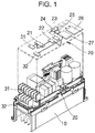
- FIG. 1 illustrates a conventional inverter and power and signal flows thereof
- FIG. 2 is a perspective view illustrating the conventional motor drive seen from another side.
- the conventional inverter includes a heat sink 10 and a plurality of circuit boards 20, 30, 40, 50, which are installed on a base.
- the heat sink 10 is installed on the base.
- the circuit boards 20, 30, 40, 50 are disposed on a middle base, which is disposed on the heat sink 10.
- the circuit boards 20, 30, 40, 50 include a power board 20 disposed on the middle base, a cap board 50 disposed on the power board 20, a control board 30 perpendicularly connected to the power board 20, and an I/O board 40 disposed on control board 30.
- the hollow arrow indicates flow of a main power along an input terminal 31, a rectification part 22, a DC link 27, an inverter part 23, and an output terminal 32.
- the solid arrow indicates an SMPS secondary power source 25, which supplies power to the control board 30, a gate drive, and a sensing and protection circuit 26.
- the dotted arrow indicates signals of a controller 24 of the control board 30, the gate drive and the sensing and protection circuit 26.
- a power terminal for the conventional inverter, a power terminal, a power unit such as PIM, and a signal unit are installed on the same board.
- the signal of the conventional inverter is structurally subjected to interference by the flow of main power as described above.
- the conventional I/O board 40 and the control board 30 are electrically connected to each other through a wire 60 for signals, thereby forming a signal line.
- the I/O board 40 is connected to the power board 20 through a ground wire 70 formed on the corresponding board, and the ground wire 70 connected to the power board 20 is extended and connected to the heat sink 10.
- the conventional inverter is structurally weak as it uses wires such as a signal wire capable of functioning as a noise antenna and a ground wire.
- Prior art documents related to the present disclosure include Korean Patent Application Publication No. 10-2007-0053940 (Publication Date: May 28, 2007 ). This document discloses a flexible print circuit board preventing circuit interference among the layers.
- an inverter is provided.
- the inverter includes a base provided with a heat dissipation part, a main board disposed on the base to output an input power along an independent power flow through a rectification part and a inverter part, and a control board fixed to be electrically connected to the main board to form a flow of a secondary power and a flow of an electrical signal, the flow of the secondary power and the flow of the electrical signal being independent from each other.
- the main board includes an input power connection part to receive the input power, the rectification part, a DC link, an inverter part, and an output terminal.
- the independent power flow is formed through the input power connection part, the rectification part, the DC link, the inverter part, and the output terminal.
- the main board further includes an SMPS power connection part.
- control board includes an SMPS power input unit electrically connected to the SMPS power connection part to input the secondary power, a controller, an SMPS power unit, and a signal unit.
- the SMPS power unit generates the secondary power and forms the flow of the second power transmitted to the controller and the signal unit.
- a signal flow is formed between the controller and the signal unit.
- the main board is grounded by contacting a metal rod connected to the heat dissipation part, the metal rod penetrating the main board.
- control board is provided with a ground connection part.
- a ground screw is installed at the ground connection part, the ground screw contacting the heat dissipation part.
- control board is electrically connected to an I/O board disposed on the main board, the control board fixing the I/O board.
- the I/O board is provided with a pattern connected to the ground connection part.
- a signal unit and a power unit are structurally separated from each other. Thereby, noise may be efficiently attenuated during operation.
- FIG. 3 is a perspective view illustrating an inverter and power and signal flows according to an embodiment of the present disclosure
- FIG. 4 is a perspective view illustrating arrangement of a main board according to an embodiment of the present disclosure
- FIG. 5 illustrates power flow according to an embodiment of the present disclosure.
- the butter according to an embodiment includes a base 100, a heat dissipation part 120, a main board 200, an EMC board 300, and a control board 400.
- An I/O board is not shown.
- the heat dissipation part 120 is installed on the base 100.
- the area of the heat dissipation part 120 is smaller than the area of the base 100.
- a side portion of the heat dissipation part 120 is provided with a heat dissipation fan 110, which is exposed to the outside.
- the main board 200 is disposed at the upper end of the heat dissipation part 120.
- the area of the main board 200 may be larger than the area for installation of the heat dissipation part 120.
- a plurality of DC links 260 is fitted into the main board 200.
- the plurality of DC links 260 may protrude downward from the main board 200 and be disposed at the side portion of the heat dissipation part 120.
- the DC links 260 may not protrude upward from the main board 200.
- the EMC board 300 is installed at an upper portion of the main board 200, and an EMC filter 310 is mounted on the EMC board 300.
- An input terminal 510 is disposed at one side of the main board 200 and an output terminal 520 is positioned adjacent to the input terminal 510.
- the main board 200 includes an input power connection part 210 (see FIG. 5 ), a rectification part 220, the DC links 260, the inverter part 270, and the output terminal 520.
- control board 400 is perpendicularly installed so as to be electrically connected and fixed to the side portion of the main board 200.
- the lower end portion of the control board 400 is preferably disposed so as to be exposed to a side portion of the heat dissipation part 120. That is, the lower end portion of the control board 400 may be exposed to the side portion of the heat dissipation part 120, thereby readily dissipating heat.
- control board 400 includes a SMPS power input unit 411 (see FIG. 8 ), a controller 420, an SMPS power unit 410, and a signal unit 430.
- the SMPS power input unit 411 is electrically connected to an SMPS power connection part formed on the main board 200.
- the SMPS power connection part will be described later.
- the heat dissipation part 120 is formed of aluminum.
- control board 400 is provided with a ground connection part 451.
- a ground screw 450 contacting the heat dissipation part 120 is installed on the ground connection part 451.
- control board 400 may fix an I/O board disposed on the main board 200 by being electrically connected to the I/O board.
- the I/O board is provided with a pattern connected to the ground connection part 451.
- the hollow arrow indicates flow of a main power along the input terminal 510, the rectification part 220, the DC links 260, the inverter part 270, and the output terminal 520.
- the solid arrow indicates flow of a secondary power of SMP supplied from the SMPS power unit 410 to the controller 420 and the sensing and protection circuit unit 430.
- a signal flow is formed between the controller 420 and the sensing and protection circuit unit 430.
- intersection of main power flows does not occur.
- the boards 200, 300, 400 are structurally separated from each other. Thereby, interference between signal flows may be prevented.
- an input AC power is applied to the rectification part 220 via the input power connection part 210 connected to the input terminal 510.
- the DC power obtained through the rectification part 220 is transmitted to the DC links 260, and the DC links 260 make the DC power smooth.
- the DC power After passing through the DC links 260, the DC power is applied to the inverter part 270.
- a connector 401 is installed at a side portion of the main board 200.
- the connector 401 is electrically connected to the control board 400 to transfer a signal.
- a PWM signal from the control board 400 is transmitted to the inverter part 270 through the connector 401.
- the inverter part 270 may output an AC power to the outside via the output terminal 520.
- an SMPS power connection part 240 is installed on the main board 200.
- FIG. 6 illustrates power flow on an EMC board according to an embodiment of the present disclosure.
- the EMC board 300 is disposed on the main board 200.
- a ground screw 321 is installed on the EMC board 300.
- the ground screw 321 is fastened to the metal rod 320, which protrudes upward through the main board 200 described above.
- an EMC filter 310 and an input power connection part 210 are installed on the EMC board 300.
- the EMC filter 310 is not electrically connected to either the input power connection part 210 or the output terminal 520.
- Power flow on EMC board 300 is formed as follows.
- An AC power input from the input terminal 510 may be transmitted to the main board 200 via the EMC filter 310 and the input power connection part 210.
- the reference numeral "511" indicates a ground terminal block.
- FIG. 7 is a perspective view illustrating installation of a control board according to an embodiment of the present disclosure.
- the main board 200 of this embodiment includes an SMPS power connection part 250.
- control board 400 includes an SMPS power input unit 411 electrically connected to the SMPS power connection part 250 to input a secondary power, a controller, an SMPS power unit 410, and a signal unit 430.
- a sensing and protection circuit unit 430 and a gate drive 470 are installed on the control board 400.
- the SMPS power unit 410 generates the secondary power. Thereby, the SMPS power unit 410 forms flow of the second power transmitted to the controller 420 and signal unit 430 and forms a signal flow between the controller 420 and signal unit 430.
- a secondary power used for control, sensing and protection is generated by the SMPS power unit 410.
- the generated a secondary power is supplied to a DSP 460, the sensing and protection circuit unit 430, and the gate drive 440 to drive the inverter part 270.
- control board 400 to drive the inverter part 270 may be structurally separated from the main board 200 serving as a power unit forming power flow.
- the signal unit is structurally separated from the power unit. Therefore, noise may be efficiently attenuated during operation.
- the main board 200 may be grounded as the metal rod 320 connected to the heat dissipation part 120 contacts the main board 200 in the penetrating manner.
- a ground connection part (not shown) may be formed on the control board 400.
- a ground screw 450 contacting the heat dissipation part 120 is installed on the ground connection part.
- another connector 402 may be formed on the control board 400 and be electrically connected to the I/O board disposed on the main board 200, thereby fixing the I/O board.
- the I/O board may be provided with an inverter connected to the ground connection part.
- the present disclosure may be grounded to the heat dissipation part using a metal rod, a ground screw, and a circuit pattern rather than using a wire.
Landscapes
- Engineering & Computer Science (AREA)
- Microelectronics & Electronic Packaging (AREA)
- Power Engineering (AREA)
- Physics & Mathematics (AREA)
- Thermal Sciences (AREA)
- Inverter Devices (AREA)
Abstract
Description
- The present disclosure relates to an inverter, and more particularly, to an inverter capable of attenuating noise during operation by structurally separating a signal unit from a power unit.
- Typically, a motor drive device is supplied with power from a commercial power source. Then, the motor driving device varies the voltage and frequency of the power and supplies the varied power to the motor, thereby controlling the speed of the motor with high efficiency. A conventional motor configured as above is described below.
-
FIG. 1 illustrates a conventional inverter and power and signal flows thereof, andFIG. 2 is a perspective view illustrating the conventional motor drive seen from another side. - Referring to
FIGS. 1 and2 , the conventional inverter includes aheat sink 10 and a plurality ofcircuit boards - The
heat sink 10 is installed on the base. - The
circuit boards heat sink 10. - The
circuit boards power board 20 disposed on the middle base, acap board 50 disposed on thepower board 20, acontrol board 30 perpendicularly connected to thepower board 20, and an I/O board 40 disposed oncontrol board 30. - In
FIG. 1 , the hollow arrow indicates flow of a main power along aninput terminal 31, arectification part 22, aDC link 27, aninverter part 23, and anoutput terminal 32. - The solid arrow indicates an SMPS
secondary power source 25, which supplies power to thecontrol board 30, a gate drive, and a sensing andprotection circuit 26. - The dotted arrow indicates signals of a
controller 24 of thecontrol board 30, the gate drive and the sensing andprotection circuit 26. - In the case of power flow and signal flow of the conventional inverter described above, interference occurs between the output of the
rectification part 22 and the output ofinverter part 23 due to intersection of main power therebetween. - That is, for the conventional inverter, a power terminal, a power unit such as PIM, and a signal unit are installed on the same board.
- Accordingly, the signal of the conventional inverter is structurally subjected to interference by the flow of main power as described above.
- Referring to
FIG. 2 , the conventional I/O board 40 and thecontrol board 30 are electrically connected to each other through awire 60 for signals, thereby forming a signal line. - The I/
O board 40 is connected to thepower board 20 through aground wire 70 formed on the corresponding board, and theground wire 70 connected to thepower board 20 is extended and connected to theheat sink 10. - According to the configuration described above, the conventional inverter is structurally weak as it uses wires such as a signal wire capable of functioning as a noise antenna and a ground wire.
- In addition, in the conventional cases, as the wires are used, fire may be caused by contact between the wires and a component generating heat in the process of assembling a product. Thereby, damage to the product and malfunctioning may occur.
- Prior art documents related to the present disclosure include
Korean Patent Application Publication No. 10-2007-0053940 (Publication Date: May 28, 2007 - It is an object of the present disclosure to provide an inverter capable of attenuating noise during operation by structurally separating a signal unit from a power unit.
- Objects of the present disclosure are not limited to the above-described objects and other objects and advantages can be appreciated by those skilled in the art from the following descriptions. Further, it will be easily appreciated that the objects and advantages of the present disclosure can be practiced by means recited in the appended claims and a combination thereof.
- In accordance with one aspect of the present disclosure, an inverter is provided.
- The inverter includes a base provided with a heat dissipation part, a main board disposed on the base to output an input power along an independent power flow through a rectification part and a inverter part, and a control board fixed to be electrically connected to the main board to form a flow of a secondary power and a flow of an electrical signal, the flow of the secondary power and the flow of the electrical signal being independent from each other.
- Preferably, the main board includes an input power connection part to receive the input power, the rectification part, a DC link, an inverter part, and an output terminal.
- Preferably, the independent power flow is formed through the input power connection part, the rectification part, the DC link, the inverter part, and the output terminal.
- Preferably, the main board further includes an SMPS power connection part.
- Preferably, the control board includes an SMPS power input unit electrically connected to the SMPS power connection part to input the secondary power, a controller, an SMPS power unit, and a signal unit.
- Preferably, the SMPS power unit generates the secondary power and forms the flow of the second power transmitted to the controller and the signal unit.
- Preferably, a signal flow is formed between the controller and the signal unit.
- Preferably, the main board is grounded by contacting a metal rod connected to the heat dissipation part, the metal rod penetrating the main board.
- Preferably, the control board is provided with a ground connection part.
- Preferably, a ground screw is installed at the ground connection part, the ground screw contacting the heat dissipation part.
- Preferably, the control board is electrically connected to an I/O board disposed on the main board, the control board fixing the I/O board.
- Preferably, the I/O board is provided with a pattern connected to the ground connection part.
- According to an embodiment of the present disclosure, a signal unit and a power unit are structurally separated from each other. Thereby, noise may be efficiently attenuated during operation.
- Further, multiple boards combined to be electrically connected to each other are grounded to a heat dissipation part serving as a heat sink, using a ground screw and a metal rod rather than using a wire. Thereby, the problems resulting from use of wires in the prior art may be addressed.
-
-
FIG. 1 illustrates a conventional inverter and power and signal flows thereof. -
FIG. 2 illustrates the structure of the conventional inverter. -
FIG. 3 is a perspective view illustrating an inverter and power and signal flows according to an embodiment of the present disclosure. -
FIG. 4 is a perspective view illustrating arrangement of a main board according to an embodiment of the present disclosure. -
FIG. 5 illustrates power flow according to an embodiment of the present disclosure. -
FIG. 6 illustrates power flow on an EMC board according to an embodiment of the present disclosure. -
FIG. 7 is a perspective view illustrating installation of a control board according to an embodiment of the present disclosure. -
FIG. 8 illustrates flow of a secondary power and a signal on a control board. - The above objects, features and advantages will become apparent from the detailed description with reference to the accompanying drawings. Embodiments are described in sufficient detail to enable those skilled in the art in the art to easily practice the technical idea of the present disclosure. Detailed descriptions of well known functions or configurations may be omitted in order not to unnecessarily obscure the gist of the present disclosure. Hereinafter, embodiments of the present disclosure will be described in detail with reference to the accompanying drawings. Throughout the drawings, like reference numerals refer to like elements.
-
FIG. 3 is a perspective view illustrating an inverter and power and signal flows according to an embodiment of the present disclosure,FIG. 4 is a perspective view illustrating arrangement of a main board according to an embodiment of the present disclosure, andFIG. 5 illustrates power flow according to an embodiment of the present disclosure. - Hereinafter, the structure of an inverter according to an embodiment of the present disclosure will be described with reference to
FIG. 3 . - Referring to
FIG. 3 , the butter according to an embodiment includes abase 100, aheat dissipation part 120, amain board 200, an EMCboard 300, and acontrol board 400. An I/O board is not shown. - The
heat dissipation part 120 is installed on thebase 100. The area of theheat dissipation part 120 is smaller than the area of thebase 100. - A side portion of the
heat dissipation part 120 is provided with aheat dissipation fan 110, which is exposed to the outside. - The
main board 200 is disposed at the upper end of theheat dissipation part 120. - Herein, the area of the
main board 200 may be larger than the area for installation of theheat dissipation part 120. - A plurality of
DC links 260 is fitted into themain board 200. - The plurality of
DC links 260 may protrude downward from themain board 200 and be disposed at the side portion of theheat dissipation part 120. - Accordingly, the DC links 260 may not protrude upward from the
main board 200. - In addition, the
EMC board 300 is installed at an upper portion of themain board 200, and anEMC filter 310 is mounted on theEMC board 300. - An
input terminal 510 is disposed at one side of themain board 200 and anoutput terminal 520 is positioned adjacent to theinput terminal 510. - The
main board 200 includes an input power connection part 210 (seeFIG. 5 ), arectification part 220, the DC links 260, theinverter part 270, and theoutput terminal 520. - In this embodiment, the
control board 400 is perpendicularly installed so as to be electrically connected and fixed to the side portion of themain board 200. - Herein, the lower end portion of the
control board 400 is preferably disposed so as to be exposed to a side portion of theheat dissipation part 120. That is, the lower end portion of thecontrol board 400 may be exposed to the side portion of theheat dissipation part 120, thereby readily dissipating heat. - Herein, the
control board 400 includes a SMPS power input unit 411 (seeFIG. 8 ), acontroller 420, anSMPS power unit 410, and asignal unit 430. - The SMPS
power input unit 411 is electrically connected to an SMPS power connection part formed on themain board 200. The SMPS power connection part will be described later. - Meanwhile, the
main board 200 is grounded to ametal rod 320 connected to theheat dissipation part 120 as themetal rod 320 contacts themain board 200 in a penetrating manner. Theheat dissipation part 120 is formed of aluminum. - In addition, the
control board 400 is provided with a ground connection part 451. - A
ground screw 450 contacting theheat dissipation part 120 is installed on the ground connection part 451. - Additionally, although not shown in the figure, the
control board 400 may fix an I/O board disposed on themain board 200 by being electrically connected to the I/O board. - The I/O board is provided with a pattern connected to the ground connection part 451.
- Next, a description will be given of a signal flow system according to independent formation of power flow and signal flow through the inverter of the present disclosure configured as above.
- Hereinafter, power flow of the inverter according to an embodiment will be described with reference to
FIG. 3 . - In
FIG. 3 , the hollow arrow indicates flow of a main power along theinput terminal 510, therectification part 220, the DC links 260, theinverter part 270, and theoutput terminal 520. - In addition, the solid arrow indicates flow of a secondary power of SMP supplied from the
SMPS power unit 410 to thecontroller 420 and the sensing andprotection circuit unit 430. - In addition, a signal flow is formed between the
controller 420 and the sensing andprotection circuit unit 430. - As described above, according to an embodiment of the present disclosure, intersection of main power flows does not occur.
- That is, in this embodiment, in implementing power flow and signal flow, the
boards - Referring to
FIGS. 4 and5 , an input AC power is applied to therectification part 220 via the inputpower connection part 210 connected to theinput terminal 510. - Subsequently, the DC power obtained through the
rectification part 220 is transmitted to the DC links 260, and the DC links 260 make the DC power smooth. - After passing through the DC links 260, the DC power is applied to the
inverter part 270. - Herein, a
connector 401 is installed at a side portion of themain board 200. - The
connector 401 is electrically connected to thecontrol board 400 to transfer a signal. - Herein, a PWM signal from the
control board 400 is transmitted to theinverter part 270 through theconnector 401. - In addition, the
inverter part 270 may output an AC power to the outside via theoutput terminal 520. - In addition, an SMPS
power connection part 240 is installed on themain board 200. -
FIG. 6 illustrates power flow on an EMC board according to an embodiment of the present disclosure. - Referring to
FIG. 6 , theEMC board 300 is disposed on themain board 200. - A
ground screw 321 is installed on theEMC board 300. - The
ground screw 321 is fastened to themetal rod 320, which protrudes upward through themain board 200 described above. - Herein, an
EMC filter 310 and an inputpower connection part 210 are installed on theEMC board 300. - The
EMC filter 310 is not electrically connected to either the inputpower connection part 210 or theoutput terminal 520. - Power flow on
EMC board 300 is formed as follows. - An AC power input from the
input terminal 510 may be transmitted to themain board 200 via theEMC filter 310 and the inputpower connection part 210. - The reference numeral "511" indicates a ground terminal block.
-
FIG. 7 is a perspective view illustrating installation of a control board according to an embodiment of the present disclosure. - Referring to
FIGS. 7 and8 , themain board 200 of this embodiment includes an SMPSpower connection part 250. - In addition, the
control board 400 includes an SMPSpower input unit 411 electrically connected to the SMPSpower connection part 250 to input a secondary power, a controller, anSMPS power unit 410, and asignal unit 430. - In addition, a sensing and
protection circuit unit 430 and a gate drive 470 are installed on thecontrol board 400. - The
SMPS power unit 410 generates the secondary power. Thereby, theSMPS power unit 410 forms flow of the second power transmitted to thecontroller 420 andsignal unit 430 and forms a signal flow between thecontroller 420 andsignal unit 430. - When the power is input from the SMPS
power connection part 250 to the SMPSpower input unit 411, a secondary power used for control, sensing and protection is generated by theSMPS power unit 410. - The generated a secondary power is supplied to a DSP 460, the sensing and
protection circuit unit 430, and thegate drive 440 to drive theinverter part 270. - Thereby, the
control board 400 to drive theinverter part 270 may be structurally separated from themain board 200 serving as a power unit forming power flow. - According to the configuration and operation described above, in this embodiment, the signal unit is structurally separated from the power unit. Thereby, noise may be efficiently attenuated during operation.
- The
main board 200 may be grounded as themetal rod 320 connected to theheat dissipation part 120 contacts themain board 200 in the penetrating manner. - In addition, a ground connection part (not shown) may be formed on the
control board 400. - Additionally, a
ground screw 450 contacting theheat dissipation part 120 is installed on the ground connection part. - Further, another
connector 402 may be formed on thecontrol board 400 and be electrically connected to the I/O board disposed on themain board 200, thereby fixing the I/O board. - The I/O board may be provided with an inverter connected to the ground connection part.
- According to the configuration and operation described above, the present disclosure may be grounded to the heat dissipation part using a metal rod, a ground screw, and a circuit pattern rather than using a wire. Thereby, the problems of the conventional technology such as damage to a product, malfunctioning and fire, which may occur in the event that the wire contacts a heat dissipating component in the product in the process of assembling the product, may be efficiently addressed.
- Although embodiments of an inverter having a noise attenuation structure have been described above, it is apparent to those skilled in the art that various changes may be made to the present disclosure without departing from the scope of the present disclosure.
- Therefore, the scope of the present disclosure should not be limited to the embodiments described above, and should be defined by the claims accompanying claims and equivalents thereof.
- The present disclosure described above may be variously substituted, altered, and modified by those skilled in the art to which the present disclosure pertains without departing from the scope and sprit of the present disclosure. Therefore, the present disclosure is not limited to the above-mentioned exemplary embodiments and the accompanying drawings.
Claims (6)
- An inverter comprising:a base (100) provided with a heat dissipation part (120);a main board (200) disposed on the base (100) to output an input power along an independent power flow through a rectification part (220) and a inverter part (270); anda control board (400) fixed to be electrically connected to the main board (200) to form a flow of a secondary power and a flow of an electrical signal, the flow of the secondary power and the flow of the electrical signal being independent from each other,wherein the main board (200) comprises an input power connection part (210) to receive the input power, the rectification part (220), a DC link (260), an inverter part (270), and an output terminal (520).
- The inverter according to claim 1, wherein an area of the main board (200) is larger than an area for installation of the heat dissipation part (120),
wherein the independent power flow is formed through the input power connection part (210), the rectification part (220), the DC link (260), the inverter part (270), and the output terminal (520). - The inverter according to claim 2, wherein the main board (200) further comprises an SMPS power connection part (240),
wherein the control board (400) is fixed to a side portion of the main board (200), the control board (400) comprising:an SMPS power input unit (411) electrically connected to the SMPS power connection part (240) to input the secondary power, a controller (420), an SMPS power unit (410), and a signal unit (430),wherein the SMPS power unit (410) generates the secondary power and forms the flow of the second power transmitted to the controller (420) and the signal unit (430),wherein a signal flow is formed between the controller (420) and the signal unit (430). - The inverter according to claim 1, wherein the main board (200) is grounded by contacting a metal rod connected to the heat dissipation part 120, the metal rod penetrating the main board (200).
- The inverter according to claim 4, wherein the control board (400) is provided with a ground connection part (451),
wherein a ground screw is installed at the ground connection part (451), the ground screw contacting the heat dissipation part (120). - The inverter according to claim 5, wherein the control board (400) is electrically connected to an I/O board disposed on the main board (200), the control board (400) fixing the I/O board,
wherein the I/O board is provided with a pattern connected to the ground connection part (451).
Applications Claiming Priority (1)
| Application Number | Priority Date | Filing Date | Title |
|---|---|---|---|
| KR1020160021748A KR101821878B1 (en) | 2016-02-24 | 2016-02-24 | Inverter |
Publications (2)
| Publication Number | Publication Date |
|---|---|
| EP3211979A1 true EP3211979A1 (en) | 2017-08-30 |
| EP3211979B1 EP3211979B1 (en) | 2021-06-09 |
Family
ID=57909461
Family Applications (1)
| Application Number | Title | Priority Date | Filing Date |
|---|---|---|---|
| EP17152806.0A Active EP3211979B1 (en) | 2016-02-24 | 2017-01-24 | Inverter |
Country Status (6)
| Country | Link |
|---|---|
| US (1) | US9929669B2 (en) |
| EP (1) | EP3211979B1 (en) |
| JP (1) | JP6580609B2 (en) |
| KR (1) | KR101821878B1 (en) |
| CN (1) | CN107124109B (en) |
| ES (1) | ES2883238T3 (en) |
Cited By (3)
| Publication number | Priority date | Publication date | Assignee | Title |
|---|---|---|---|---|
| EP3518637A1 (en) * | 2018-01-29 | 2019-07-31 | LSIS Co., Ltd. | Device for driving motor |
| EP3565393A1 (en) * | 2018-05-02 | 2019-11-06 | LSIS Co., Ltd. | Device for driving motor |
| EP3934087A4 (en) * | 2019-02-25 | 2022-12-07 | LS Electric Co., Ltd. | ELECTRIC MOTOR DRIVE DEVICE |
Families Citing this family (6)
| Publication number | Priority date | Publication date | Assignee | Title |
|---|---|---|---|---|
| CN109412390B (en) * | 2017-08-15 | 2020-09-25 | 泰达电子股份有限公司 | Power conversion device |
| DE102017120924B4 (en) * | 2017-09-11 | 2025-07-03 | Hanon Systems | EMC filter to suppress interference signals |
| WO2019130481A1 (en) * | 2017-12-27 | 2019-07-04 | 株式会社安川電機 | Inverter device |
| KR102478290B1 (en) * | 2018-04-26 | 2022-12-16 | 엘에스일렉트릭(주) | Device for driving motor |
| CN112423562A (en) * | 2020-12-03 | 2021-02-26 | 青岛中加特电气股份有限公司 | Frequency conversion cabinet for electric fracturing truck pump |
| WO2023240236A1 (en) | 2022-06-10 | 2023-12-14 | Voyager Therapeutics, Inc. | Compositions and methods for the treatment of spinal muscular atrophy related disorders |
Citations (3)
| Publication number | Priority date | Publication date | Assignee | Title |
|---|---|---|---|---|
| US5555159A (en) * | 1993-12-17 | 1996-09-10 | Schneider Electric Sa | Add-on module for variable speed drives |
| KR20070053940A (en) | 2005-11-22 | 2007-05-28 | 엘지전자 주식회사 | Flexible Circuit Boards Preventing Interlayer Interference |
| US20130294040A1 (en) * | 2010-12-27 | 2013-11-07 | Hitachi Automotive Systems, Ltd. | Electrical Converter |
Family Cites Families (43)
| Publication number | Priority date | Publication date | Assignee | Title |
|---|---|---|---|---|
| IL116111A0 (en) * | 1995-11-23 | 1997-11-20 | Magnify Electronic Systems 199 | Uninterruptible power system card |
| US5835350A (en) * | 1996-12-23 | 1998-11-10 | Lucent Technologies Inc. | Encapsulated, board-mountable power supply and method of manufacture therefor |
| US6201701B1 (en) * | 1998-03-11 | 2001-03-13 | Kimball International, Inc. | Integrated substrate with enhanced thermal characteristics |
| US6657320B1 (en) * | 1999-11-03 | 2003-12-02 | Active Power, Inc. | Integrated flywheel uninterruptible power supply system |
| US6362964B1 (en) * | 1999-11-17 | 2002-03-26 | International Rectifier Corp. | Flexible power assembly |
| US6434003B1 (en) * | 2001-04-24 | 2002-08-13 | York International Corporation | Liquid-cooled power semiconductor device heatsink |
| US6987670B2 (en) * | 2003-05-16 | 2006-01-17 | Ballard Power Systems Corporation | Dual power module power system architecture |
| KR100625971B1 (en) * | 2003-10-10 | 2006-09-20 | 삼성에스디아이 주식회사 | Plasma display device with improved coupling and grounding structure of circuit board |
| JP2005331945A (en) * | 2004-05-18 | 2005-12-02 | Samsung Sdi Co Ltd | Plasma display device |
| US7289329B2 (en) * | 2004-06-04 | 2007-10-30 | Siemens Vdo Automotive Corporation | Integration of planar transformer and/or planar inductor with power switches in power converter |
| JP2009071992A (en) * | 2007-09-13 | 2009-04-02 | Yaskawa Electric Corp | Electric motor control device |
| JP5264189B2 (en) * | 2008-01-10 | 2013-08-14 | 三菱電機株式会社 | Inverter device and manufacturing method thereof |
| US7616442B1 (en) * | 2008-04-25 | 2009-11-10 | Rockwell Automation Technologies, Inc. | Power electronic module cooling system and method |
| JP5407198B2 (en) * | 2008-07-02 | 2014-02-05 | 富士電機株式会社 | Power module for power converter |
| JP5319979B2 (en) | 2008-07-28 | 2013-10-16 | 株式会社ケーヒン | Terminal with busbar |
| JP4657329B2 (en) * | 2008-07-29 | 2011-03-23 | 日立オートモティブシステムズ株式会社 | Power converter and electric vehicle |
| US8248009B2 (en) * | 2008-11-17 | 2012-08-21 | Rockwell Automation Technologies, Inc. | Motor controller having integrated communications configurations |
| JP5260347B2 (en) * | 2009-02-06 | 2013-08-14 | 日立オートモティブシステムズ株式会社 | Power converter |
| JP5344182B2 (en) * | 2010-02-02 | 2013-11-20 | 株式会社安川電機 | Power converter |
| JP5201171B2 (en) * | 2010-05-21 | 2013-06-05 | 株式会社デンソー | Semiconductor module and driving device using the same |
| JP5206732B2 (en) * | 2010-05-21 | 2013-06-12 | 株式会社デンソー | Inverter device and drive device using the same |
| JP5601912B2 (en) | 2010-07-09 | 2014-10-08 | 株式会社ダイヘン | Control device for power converter, and grid-connected inverter system using this control device |
| WO2012056735A1 (en) * | 2010-10-27 | 2012-05-03 | 三菱電機株式会社 | Device for controlling drive of motor for electric power steering device |
| KR101189451B1 (en) * | 2010-12-24 | 2012-10-09 | 엘지전자 주식회사 | Inverter stack |
| US9237679B2 (en) * | 2011-02-04 | 2016-01-12 | Sew-Eurodrive Gmbh & Co. Kg | Electrical device |
| JP5825843B2 (en) * | 2011-05-19 | 2015-12-02 | 株式会社日立製作所 | Semiconductor unit and power conversion device |
| EP2574157A1 (en) * | 2011-09-23 | 2013-03-27 | AEG Power Solutions B.V. | High-power electronics component and assembly comprising at least one such high-power electronics component |
| JP5673857B2 (en) * | 2011-11-21 | 2015-02-18 | 株式会社オートネットワーク技術研究所 | DC-DC converter |
| WO2013088518A1 (en) * | 2011-12-13 | 2013-06-20 | 三菱電機株式会社 | Motor with built-in power conversion device, air conditioner with same motor built-in, water heater, and ventilation blower equipment |
| JP5749192B2 (en) * | 2012-02-13 | 2015-07-15 | 株式会社東芝 | Vehicle drive control device |
| US8811015B2 (en) * | 2012-02-16 | 2014-08-19 | Mission Motor Company | Motor control device |
| JP5738794B2 (en) * | 2012-03-30 | 2015-06-24 | 日立オートモティブシステムズ株式会社 | Power converter |
| JP5753829B2 (en) * | 2012-09-28 | 2015-07-22 | 日立オートモティブシステムズ株式会社 | Power converter |
| JP5884775B2 (en) | 2013-05-31 | 2016-03-15 | 株式会社豊田自動織機 | Inverter device |
| KR101768256B1 (en) | 2013-08-29 | 2017-08-14 | 엘에스산전 주식회사 | Inverter with power cell of dual structure |
| JP2015193371A (en) * | 2014-03-27 | 2015-11-05 | 日本電産エレシス株式会社 | Electronic control device for electric power steering |
| US9504191B2 (en) * | 2014-03-28 | 2016-11-22 | Deere & Company | Electronic assembly for an inverter |
| US9362609B2 (en) * | 2014-03-31 | 2016-06-07 | Raytheon Company | Modular spatially combined EHF power amplifier |
| KR20160011867A (en) * | 2014-07-23 | 2016-02-02 | 엘에스산전 주식회사 | Inverter assembly without galvanic isolation |
| FI126380B (en) * | 2014-10-27 | 2016-11-15 | Kone Corp | operating unit |
| US9420724B2 (en) * | 2014-11-04 | 2016-08-16 | Ge Aviation Systems Llc | Power converter assembly |
| TWI590571B (en) * | 2014-12-08 | 2017-07-01 | 強生控制科技公司 | Variable speed drive system and cooling system |
| CN204887686U (en) * | 2015-09-09 | 2015-12-16 | 武汉华中数控股份有限公司 | A PCB board grounding structure |
-
2016
- 2016-02-24 KR KR1020160021748A patent/KR101821878B1/en active Active
-
2017
- 2017-01-24 EP EP17152806.0A patent/EP3211979B1/en active Active
- 2017-01-24 ES ES17152806T patent/ES2883238T3/en active Active
- 2017-01-26 JP JP2017012480A patent/JP6580609B2/en not_active Expired - Fee Related
- 2017-02-06 CN CN201710067165.4A patent/CN107124109B/en active Active
- 2017-02-07 US US15/426,378 patent/US9929669B2/en active Active
Patent Citations (3)
| Publication number | Priority date | Publication date | Assignee | Title |
|---|---|---|---|---|
| US5555159A (en) * | 1993-12-17 | 1996-09-10 | Schneider Electric Sa | Add-on module for variable speed drives |
| KR20070053940A (en) | 2005-11-22 | 2007-05-28 | 엘지전자 주식회사 | Flexible Circuit Boards Preventing Interlayer Interference |
| US20130294040A1 (en) * | 2010-12-27 | 2013-11-07 | Hitachi Automotive Systems, Ltd. | Electrical Converter |
Cited By (6)
| Publication number | Priority date | Publication date | Assignee | Title |
|---|---|---|---|---|
| EP3518637A1 (en) * | 2018-01-29 | 2019-07-31 | LSIS Co., Ltd. | Device for driving motor |
| US10716237B2 (en) | 2018-01-29 | 2020-07-14 | Lsis Co., Ltd. | Device for driving motor |
| EP3565393A1 (en) * | 2018-05-02 | 2019-11-06 | LSIS Co., Ltd. | Device for driving motor |
| US10490917B1 (en) | 2018-05-02 | 2019-11-26 | Lsis Co., Ltd. | Device for driving motor |
| EP3934087A4 (en) * | 2019-02-25 | 2022-12-07 | LS Electric Co., Ltd. | ELECTRIC MOTOR DRIVE DEVICE |
| US12027923B2 (en) | 2019-02-25 | 2024-07-02 | Ls Electric Co., Ltd. | Electric motor driving device |
Also Published As
| Publication number | Publication date |
|---|---|
| US20170244335A1 (en) | 2017-08-24 |
| CN107124109A (en) | 2017-09-01 |
| US9929669B2 (en) | 2018-03-27 |
| KR101821878B1 (en) | 2018-01-24 |
| ES2883238T3 (en) | 2021-12-07 |
| EP3211979B1 (en) | 2021-06-09 |
| KR20170099547A (en) | 2017-09-01 |
| JP2017153349A (en) | 2017-08-31 |
| JP6580609B2 (en) | 2019-09-25 |
| CN107124109B (en) | 2020-09-15 |
Similar Documents
| Publication | Publication Date | Title |
|---|---|---|
| US9929669B2 (en) | Inverter | |
| US10177674B2 (en) | Power circuit device | |
| JP4784493B2 (en) | Separately powered LED lighting device | |
| JP6719021B2 (en) | Power converter | |
| TW200922418A (en) | Device mounting structure and device mounting method | |
| EP3024307B1 (en) | Power control assembly with vertically mounted power devices | |
| JP6176135B2 (en) | Power converter | |
| US7902464B2 (en) | Heat sink arrangement for electrical apparatus | |
| JP6873217B1 (en) | Power converter | |
| JP6076174B2 (en) | Control device with high noise resistance | |
| DE102012014011A1 (en) | Electrical appliance for supplying power to e.g. asynchronous motor, has optical coupler connected with power module, in high voltage region, by parallely arranged strip conductors, where strip conductors are arranged in high voltage region | |
| US9801314B2 (en) | Power source apparatus | |
| JP7465954B2 (en) | Power Conversion Equipment | |
| JP6614793B2 (en) | Electrical system with shield | |
| CN110486847B (en) | Automatically controlled subassembly, off-premises station and air conditioner | |
| JP6768856B2 (en) | Electric motor drive | |
| JP5263592B2 (en) | LED lighting device and lighting apparatus | |
| WO2020122029A1 (en) | Electronic control device | |
| WO2017126086A1 (en) | Power conversion device | |
| EP3196932A1 (en) | Cooled electrical assembly | |
| JP4385393B2 (en) | Connection structure between printed circuit board and heat sink | |
| US20180324942A1 (en) | Method for reducing conductor track spacing in electronic circuit boards and electronic circuit board with reduced spacing between conductor tracks | |
| JP2004022310A (en) | Discharge lamp lighting device | |
| JP2009224392A (en) | Power supply device | |
| JP2005056731A (en) | High frequency heating device |
Legal Events
| Date | Code | Title | Description |
|---|---|---|---|
| PUAI | Public reference made under article 153(3) epc to a published international application that has entered the european phase |
Free format text: ORIGINAL CODE: 0009012 |
|
| STAA | Information on the status of an ep patent application or granted ep patent |
Free format text: STATUS: THE APPLICATION HAS BEEN PUBLISHED |
|
| AK | Designated contracting states |
Kind code of ref document: A1 Designated state(s): AL AT BE BG CH CY CZ DE DK EE ES FI FR GB GR HR HU IE IS IT LI LT LU LV MC MK MT NL NO PL PT RO RS SE SI SK SM TR |
|
| AX | Request for extension of the european patent |
Extension state: BA ME |
|
| STAA | Information on the status of an ep patent application or granted ep patent |
Free format text: STATUS: REQUEST FOR EXAMINATION WAS MADE |
|
| 17P | Request for examination filed |
Effective date: 20180228 |
|
| RBV | Designated contracting states (corrected) |
Designated state(s): AL AT BE BG CH CY CZ DE DK EE ES FI FR GB GR HR HU IE IS IT LI LT LU LV MC MK MT NL NO PL PT RO RS SE SI SK SM TR |
|
| STAA | Information on the status of an ep patent application or granted ep patent |
Free format text: STATUS: EXAMINATION IS IN PROGRESS |
|
| 17Q | First examination report despatched |
Effective date: 20200618 |
|
| GRAP | Despatch of communication of intention to grant a patent |
Free format text: ORIGINAL CODE: EPIDOSNIGR1 |
|
| STAA | Information on the status of an ep patent application or granted ep patent |
Free format text: STATUS: GRANT OF PATENT IS INTENDED |
|
| INTG | Intention to grant announced |
Effective date: 20210217 |
|
| GRAS | Grant fee paid |
Free format text: ORIGINAL CODE: EPIDOSNIGR3 |
|
| GRAA | (expected) grant |
Free format text: ORIGINAL CODE: 0009210 |
|
| STAA | Information on the status of an ep patent application or granted ep patent |
Free format text: STATUS: THE PATENT HAS BEEN GRANTED |
|
| AK | Designated contracting states |
Kind code of ref document: B1 Designated state(s): AL AT BE BG CH CY CZ DE DK EE ES FI FR GB GR HR HU IE IS IT LI LT LU LV MC MK MT NL NO PL PT RO RS SE SI SK SM TR |
|
| REG | Reference to a national code |
Ref country code: GB Ref legal event code: FG4D |
|
| REG | Reference to a national code |
Ref country code: CH Ref legal event code: EP Ref country code: AT Ref legal event code: REF Ref document number: 1401532 Country of ref document: AT Kind code of ref document: T Effective date: 20210615 |
|
| REG | Reference to a national code |
Ref country code: DE Ref legal event code: R096 Ref document number: 602017039902 Country of ref document: DE |
|
| REG | Reference to a national code |
Ref country code: IE Ref legal event code: FG4D |
|
| REG | Reference to a national code |
Ref country code: LT Ref legal event code: MG9D |
|
| PG25 | Lapsed in a contracting state [announced via postgrant information from national office to epo] |
Ref country code: HR Free format text: LAPSE BECAUSE OF FAILURE TO SUBMIT A TRANSLATION OF THE DESCRIPTION OR TO PAY THE FEE WITHIN THE PRESCRIBED TIME-LIMIT Effective date: 20210609 Ref country code: BG Free format text: LAPSE BECAUSE OF FAILURE TO SUBMIT A TRANSLATION OF THE DESCRIPTION OR TO PAY THE FEE WITHIN THE PRESCRIBED TIME-LIMIT Effective date: 20210909 Ref country code: FI Free format text: LAPSE BECAUSE OF FAILURE TO SUBMIT A TRANSLATION OF THE DESCRIPTION OR TO PAY THE FEE WITHIN THE PRESCRIBED TIME-LIMIT Effective date: 20210609 Ref country code: LT Free format text: LAPSE BECAUSE OF FAILURE TO SUBMIT A TRANSLATION OF THE DESCRIPTION OR TO PAY THE FEE WITHIN THE PRESCRIBED TIME-LIMIT Effective date: 20210609 |
|
| REG | Reference to a national code |
Ref country code: AT Ref legal event code: MK05 Ref document number: 1401532 Country of ref document: AT Kind code of ref document: T Effective date: 20210609 |
|
| REG | Reference to a national code |
Ref country code: NL Ref legal event code: MP Effective date: 20210609 |
|
| PG25 | Lapsed in a contracting state [announced via postgrant information from national office to epo] |
Ref country code: SE Free format text: LAPSE BECAUSE OF FAILURE TO SUBMIT A TRANSLATION OF THE DESCRIPTION OR TO PAY THE FEE WITHIN THE PRESCRIBED TIME-LIMIT Effective date: 20210609 Ref country code: RS Free format text: LAPSE BECAUSE OF FAILURE TO SUBMIT A TRANSLATION OF THE DESCRIPTION OR TO PAY THE FEE WITHIN THE PRESCRIBED TIME-LIMIT Effective date: 20210609 Ref country code: NO Free format text: LAPSE BECAUSE OF FAILURE TO SUBMIT A TRANSLATION OF THE DESCRIPTION OR TO PAY THE FEE WITHIN THE PRESCRIBED TIME-LIMIT Effective date: 20210909 Ref country code: LV Free format text: LAPSE BECAUSE OF FAILURE TO SUBMIT A TRANSLATION OF THE DESCRIPTION OR TO PAY THE FEE WITHIN THE PRESCRIBED TIME-LIMIT Effective date: 20210609 Ref country code: GR Free format text: LAPSE BECAUSE OF FAILURE TO SUBMIT A TRANSLATION OF THE DESCRIPTION OR TO PAY THE FEE WITHIN THE PRESCRIBED TIME-LIMIT Effective date: 20210910 |
|
| REG | Reference to a national code |
Ref country code: ES Ref legal event code: FG2A Ref document number: 2883238 Country of ref document: ES Kind code of ref document: T3 Effective date: 20211207 |
|
| PG25 | Lapsed in a contracting state [announced via postgrant information from national office to epo] |
Ref country code: AT Free format text: LAPSE BECAUSE OF FAILURE TO SUBMIT A TRANSLATION OF THE DESCRIPTION OR TO PAY THE FEE WITHIN THE PRESCRIBED TIME-LIMIT Effective date: 20210609 Ref country code: CZ Free format text: LAPSE BECAUSE OF FAILURE TO SUBMIT A TRANSLATION OF THE DESCRIPTION OR TO PAY THE FEE WITHIN THE PRESCRIBED TIME-LIMIT Effective date: 20210609 Ref country code: EE Free format text: LAPSE BECAUSE OF FAILURE TO SUBMIT A TRANSLATION OF THE DESCRIPTION OR TO PAY THE FEE WITHIN THE PRESCRIBED TIME-LIMIT Effective date: 20210609 Ref country code: RO Free format text: LAPSE BECAUSE OF FAILURE TO SUBMIT A TRANSLATION OF THE DESCRIPTION OR TO PAY THE FEE WITHIN THE PRESCRIBED TIME-LIMIT Effective date: 20210609 Ref country code: PT Free format text: LAPSE BECAUSE OF FAILURE TO SUBMIT A TRANSLATION OF THE DESCRIPTION OR TO PAY THE FEE WITHIN THE PRESCRIBED TIME-LIMIT Effective date: 20211011 Ref country code: NL Free format text: LAPSE BECAUSE OF FAILURE TO SUBMIT A TRANSLATION OF THE DESCRIPTION OR TO PAY THE FEE WITHIN THE PRESCRIBED TIME-LIMIT Effective date: 20210609 Ref country code: SK Free format text: LAPSE BECAUSE OF FAILURE TO SUBMIT A TRANSLATION OF THE DESCRIPTION OR TO PAY THE FEE WITHIN THE PRESCRIBED TIME-LIMIT Effective date: 20210609 Ref country code: SM Free format text: LAPSE BECAUSE OF FAILURE TO SUBMIT A TRANSLATION OF THE DESCRIPTION OR TO PAY THE FEE WITHIN THE PRESCRIBED TIME-LIMIT Effective date: 20210609 |
|
| PGFP | Annual fee paid to national office [announced via postgrant information from national office to epo] |
Ref country code: GB Payment date: 20211220 Year of fee payment: 6 |
|
| PG25 | Lapsed in a contracting state [announced via postgrant information from national office to epo] |
Ref country code: PL Free format text: LAPSE BECAUSE OF FAILURE TO SUBMIT A TRANSLATION OF THE DESCRIPTION OR TO PAY THE FEE WITHIN THE PRESCRIBED TIME-LIMIT Effective date: 20210609 |
|
| REG | Reference to a national code |
Ref country code: DE Ref legal event code: R097 Ref document number: 602017039902 Country of ref document: DE |
|
| PLBE | No opposition filed within time limit |
Free format text: ORIGINAL CODE: 0009261 |
|
| STAA | Information on the status of an ep patent application or granted ep patent |
Free format text: STATUS: NO OPPOSITION FILED WITHIN TIME LIMIT |
|
| PG25 | Lapsed in a contracting state [announced via postgrant information from national office to epo] |
Ref country code: DK Free format text: LAPSE BECAUSE OF FAILURE TO SUBMIT A TRANSLATION OF THE DESCRIPTION OR TO PAY THE FEE WITHIN THE PRESCRIBED TIME-LIMIT Effective date: 20210609 |
|
| 26N | No opposition filed |
Effective date: 20220310 |
|
| PG25 | Lapsed in a contracting state [announced via postgrant information from national office to epo] |
Ref country code: AL Free format text: LAPSE BECAUSE OF FAILURE TO SUBMIT A TRANSLATION OF THE DESCRIPTION OR TO PAY THE FEE WITHIN THE PRESCRIBED TIME-LIMIT Effective date: 20210609 |
|
| PGFP | Annual fee paid to national office [announced via postgrant information from national office to epo] |
Ref country code: ES Payment date: 20220210 Year of fee payment: 6 |
|
| PG25 | Lapsed in a contracting state [announced via postgrant information from national office to epo] |
Ref country code: MC Free format text: LAPSE BECAUSE OF FAILURE TO SUBMIT A TRANSLATION OF THE DESCRIPTION OR TO PAY THE FEE WITHIN THE PRESCRIBED TIME-LIMIT Effective date: 20210609 |
|
| REG | Reference to a national code |
Ref country code: CH Ref legal event code: PL |
|
| REG | Reference to a national code |
Ref country code: BE Ref legal event code: MM Effective date: 20220131 |
|
| PG25 | Lapsed in a contracting state [announced via postgrant information from national office to epo] |
Ref country code: LU Free format text: LAPSE BECAUSE OF NON-PAYMENT OF DUE FEES Effective date: 20220124 |
|
| PG25 | Lapsed in a contracting state [announced via postgrant information from national office to epo] |
Ref country code: FR Free format text: LAPSE BECAUSE OF NON-PAYMENT OF DUE FEES Effective date: 20220131 Ref country code: BE Free format text: LAPSE BECAUSE OF NON-PAYMENT OF DUE FEES Effective date: 20220131 |
|
| PG25 | Lapsed in a contracting state [announced via postgrant information from national office to epo] |
Ref country code: LI Free format text: LAPSE BECAUSE OF NON-PAYMENT OF DUE FEES Effective date: 20220131 Ref country code: CH Free format text: LAPSE BECAUSE OF NON-PAYMENT OF DUE FEES Effective date: 20220131 |
|
| PG25 | Lapsed in a contracting state [announced via postgrant information from national office to epo] |
Ref country code: IE Free format text: LAPSE BECAUSE OF NON-PAYMENT OF DUE FEES Effective date: 20220124 |
|
| P01 | Opt-out of the competence of the unified patent court (upc) registered |
Effective date: 20230625 |
|
| GBPC | Gb: european patent ceased through non-payment of renewal fee |
Effective date: 20230124 |
|
| PG25 | Lapsed in a contracting state [announced via postgrant information from national office to epo] |
Ref country code: GB Free format text: LAPSE BECAUSE OF NON-PAYMENT OF DUE FEES Effective date: 20230124 |
|
| PG25 | Lapsed in a contracting state [announced via postgrant information from national office to epo] |
Ref country code: HU Free format text: LAPSE BECAUSE OF FAILURE TO SUBMIT A TRANSLATION OF THE DESCRIPTION OR TO PAY THE FEE WITHIN THE PRESCRIBED TIME-LIMIT; INVALID AB INITIO Effective date: 20170124 |
|
| REG | Reference to a national code |
Ref country code: ES Ref legal event code: FD2A Effective date: 20240402 |
|
| PG25 | Lapsed in a contracting state [announced via postgrant information from national office to epo] |
Ref country code: ES Free format text: LAPSE BECAUSE OF NON-PAYMENT OF DUE FEES Effective date: 20230125 |
|
| PG25 | Lapsed in a contracting state [announced via postgrant information from national office to epo] |
Ref country code: MK Free format text: LAPSE BECAUSE OF FAILURE TO SUBMIT A TRANSLATION OF THE DESCRIPTION OR TO PAY THE FEE WITHIN THE PRESCRIBED TIME-LIMIT Effective date: 20210609 Ref country code: ES Free format text: LAPSE BECAUSE OF NON-PAYMENT OF DUE FEES Effective date: 20230125 Ref country code: CY Free format text: LAPSE BECAUSE OF FAILURE TO SUBMIT A TRANSLATION OF THE DESCRIPTION OR TO PAY THE FEE WITHIN THE PRESCRIBED TIME-LIMIT Effective date: 20210609 |
|
| PG25 | Lapsed in a contracting state [announced via postgrant information from national office to epo] |
Ref country code: MT Free format text: LAPSE BECAUSE OF FAILURE TO SUBMIT A TRANSLATION OF THE DESCRIPTION OR TO PAY THE FEE WITHIN THE PRESCRIBED TIME-LIMIT Effective date: 20210609 |
|
| PG25 | Lapsed in a contracting state [announced via postgrant information from national office to epo] |
Ref country code: TR Free format text: LAPSE BECAUSE OF FAILURE TO SUBMIT A TRANSLATION OF THE DESCRIPTION OR TO PAY THE FEE WITHIN THE PRESCRIBED TIME-LIMIT Effective date: 20210609 |
|
| PGFP | Annual fee paid to national office [announced via postgrant information from national office to epo] |
Ref country code: DE Payment date: 20251208 Year of fee payment: 10 |
|
| PGFP | Annual fee paid to national office [announced via postgrant information from national office to epo] |
Ref country code: IT Payment date: 20251209 Year of fee payment: 10 |