EP3211684B1 - Organic light emitting display device having improved reflective properties and method of manufacturing the same - Google Patents
Organic light emitting display device having improved reflective properties and method of manufacturing the same Download PDFInfo
- Publication number
- EP3211684B1 EP3211684B1 EP17155064.3A EP17155064A EP3211684B1 EP 3211684 B1 EP3211684 B1 EP 3211684B1 EP 17155064 A EP17155064 A EP 17155064A EP 3211684 B1 EP3211684 B1 EP 3211684B1
- Authority
- EP
- European Patent Office
- Prior art keywords
- layer
- light emitting
- disposed
- substrate
- display device
- Prior art date
- Legal status (The legal status is an assumption and is not a legal conclusion. Google has not performed a legal analysis and makes no representation as to the accuracy of the status listed.)
- Active
Links
Images


Classifications
-
- H—ELECTRICITY
- H05—ELECTRIC TECHNIQUES NOT OTHERWISE PROVIDED FOR
- H05B—ELECTRIC HEATING; ELECTRIC LIGHT SOURCES NOT OTHERWISE PROVIDED FOR; CIRCUIT ARRANGEMENTS FOR ELECTRIC LIGHT SOURCES, IN GENERAL
- H05B33/00—Electroluminescent light sources
- H05B33/12—Light sources with substantially two-dimensional [2D] radiating surfaces
- H05B33/22—Light sources with substantially two-dimensional [2D] radiating surfaces characterised by the chemical or physical composition or the arrangement of auxiliary dielectric or reflective layers
- H05B33/24—Light sources with substantially two-dimensional [2D] radiating surfaces characterised by the chemical or physical composition or the arrangement of auxiliary dielectric or reflective layers of metallic reflective layers
-
- H—ELECTRICITY
- H10—SEMICONDUCTOR DEVICES; ELECTRIC SOLID-STATE DEVICES NOT OTHERWISE PROVIDED FOR
- H10K—ORGANIC ELECTRIC SOLID-STATE DEVICES
- H10K59/00—Integrated devices, or assemblies of multiple devices, comprising at least one organic light-emitting element covered by group H10K50/00
- H10K59/40—OLEDs integrated with touch screens
-
- H—ELECTRICITY
- H10—SEMICONDUCTOR DEVICES; ELECTRIC SOLID-STATE DEVICES NOT OTHERWISE PROVIDED FOR
- H10K—ORGANIC ELECTRIC SOLID-STATE DEVICES
- H10K50/00—Organic light-emitting devices
- H10K50/80—Constructional details
- H10K50/84—Passivation; Containers; Encapsulations
- H10K50/841—Self-supporting sealing arrangements
-
- H—ELECTRICITY
- H10—SEMICONDUCTOR DEVICES; ELECTRIC SOLID-STATE DEVICES NOT OTHERWISE PROVIDED FOR
- H10K—ORGANIC ELECTRIC SOLID-STATE DEVICES
- H10K50/00—Organic light-emitting devices
- H10K50/80—Constructional details
- H10K50/84—Passivation; Containers; Encapsulations
- H10K50/842—Containers
- H10K50/8423—Metallic sealing arrangements
-
- H—ELECTRICITY
- H10—SEMICONDUCTOR DEVICES; ELECTRIC SOLID-STATE DEVICES NOT OTHERWISE PROVIDED FOR
- H10K—ORGANIC ELECTRIC SOLID-STATE DEVICES
- H10K50/00—Organic light-emitting devices
- H10K50/80—Constructional details
- H10K50/84—Passivation; Containers; Encapsulations
- H10K50/844—Encapsulations
-
- H—ELECTRICITY
- H10—SEMICONDUCTOR DEVICES; ELECTRIC SOLID-STATE DEVICES NOT OTHERWISE PROVIDED FOR
- H10K—ORGANIC ELECTRIC SOLID-STATE DEVICES
- H10K50/00—Organic light-emitting devices
- H10K50/80—Constructional details
- H10K50/85—Arrangements for extracting light from the devices
- H10K50/856—Arrangements for extracting light from the devices comprising reflective means
-
- H—ELECTRICITY
- H10—SEMICONDUCTOR DEVICES; ELECTRIC SOLID-STATE DEVICES NOT OTHERWISE PROVIDED FOR
- H10K—ORGANIC ELECTRIC SOLID-STATE DEVICES
- H10K50/00—Organic light-emitting devices
- H10K50/80—Constructional details
- H10K50/86—Arrangements for improving contrast, e.g. preventing reflection of ambient light
- H10K50/865—Arrangements for improving contrast, e.g. preventing reflection of ambient light comprising light absorbing layers, e.g. light-blocking layers
-
- H—ELECTRICITY
- H10—SEMICONDUCTOR DEVICES; ELECTRIC SOLID-STATE DEVICES NOT OTHERWISE PROVIDED FOR
- H10K—ORGANIC ELECTRIC SOLID-STATE DEVICES
- H10K59/00—Integrated devices, or assemblies of multiple devices, comprising at least one organic light-emitting element covered by group H10K50/00
- H10K59/10—OLED displays
- H10K59/12—Active-matrix OLED [AMOLED] displays
- H10K59/122—Pixel-defining structures or layers, e.g. banks
-
- H—ELECTRICITY
- H10—SEMICONDUCTOR DEVICES; ELECTRIC SOLID-STATE DEVICES NOT OTHERWISE PROVIDED FOR
- H10K—ORGANIC ELECTRIC SOLID-STATE DEVICES
- H10K59/00—Integrated devices, or assemblies of multiple devices, comprising at least one organic light-emitting element covered by group H10K50/00
- H10K59/10—OLED displays
- H10K59/12—Active-matrix OLED [AMOLED] displays
- H10K59/126—Shielding, e.g. light-blocking means over the TFTs
-
- H—ELECTRICITY
- H10—SEMICONDUCTOR DEVICES; ELECTRIC SOLID-STATE DEVICES NOT OTHERWISE PROVIDED FOR
- H10K—ORGANIC ELECTRIC SOLID-STATE DEVICES
- H10K59/00—Integrated devices, or assemblies of multiple devices, comprising at least one organic light-emitting element covered by group H10K50/00
- H10K59/10—OLED displays
- H10K59/12—Active-matrix OLED [AMOLED] displays
- H10K59/131—Interconnections, e.g. wiring lines or terminals
-
- H—ELECTRICITY
- H10—SEMICONDUCTOR DEVICES; ELECTRIC SOLID-STATE DEVICES NOT OTHERWISE PROVIDED FOR
- H10K—ORGANIC ELECTRIC SOLID-STATE DEVICES
- H10K59/00—Integrated devices, or assemblies of multiple devices, comprising at least one organic light-emitting element covered by group H10K50/00
- H10K59/80—Constructional details
- H10K59/87—Passivation; Containers; Encapsulations
- H10K59/871—Self-supporting sealing arrangements
- H10K59/8721—Metallic sealing arrangements
-
- H—ELECTRICITY
- H10—SEMICONDUCTOR DEVICES; ELECTRIC SOLID-STATE DEVICES NOT OTHERWISE PROVIDED FOR
- H10K—ORGANIC ELECTRIC SOLID-STATE DEVICES
- H10K59/00—Integrated devices, or assemblies of multiple devices, comprising at least one organic light-emitting element covered by group H10K50/00
- H10K59/80—Constructional details
- H10K59/875—Arrangements for extracting light from the devices
- H10K59/878—Arrangements for extracting light from the devices comprising reflective means
-
- H—ELECTRICITY
- H10—SEMICONDUCTOR DEVICES; ELECTRIC SOLID-STATE DEVICES NOT OTHERWISE PROVIDED FOR
- H10K—ORGANIC ELECTRIC SOLID-STATE DEVICES
- H10K59/00—Integrated devices, or assemblies of multiple devices, comprising at least one organic light-emitting element covered by group H10K50/00
- H10K59/80—Constructional details
- H10K59/8791—Arrangements for improving contrast, e.g. preventing reflection of ambient light
- H10K59/8792—Arrangements for improving contrast, e.g. preventing reflection of ambient light comprising light absorbing layers, e.g. black layers
-
- H—ELECTRICITY
- H10—SEMICONDUCTOR DEVICES; ELECTRIC SOLID-STATE DEVICES NOT OTHERWISE PROVIDED FOR
- H10K—ORGANIC ELECTRIC SOLID-STATE DEVICES
- H10K71/00—Manufacture or treatment specially adapted for the organic devices covered by this subclass
-
- F—MECHANICAL ENGINEERING; LIGHTING; HEATING; WEAPONS; BLASTING
- F21—LIGHTING
- F21V—FUNCTIONAL FEATURES OR DETAILS OF LIGHTING DEVICES OR SYSTEMS THEREOF; STRUCTURAL COMBINATIONS OF LIGHTING DEVICES WITH OTHER ARTICLES, NOT OTHERWISE PROVIDED FOR
- F21V33/00—Structural combinations of lighting devices with other articles, not otherwise provided for
- F21V33/0004—Personal or domestic articles
- F21V33/004—Sanitary equipment, e.g. mirrors, showers, toilet seats or paper dispensers
-
- H—ELECTRICITY
- H10—SEMICONDUCTOR DEVICES; ELECTRIC SOLID-STATE DEVICES NOT OTHERWISE PROVIDED FOR
- H10K—ORGANIC ELECTRIC SOLID-STATE DEVICES
- H10K59/00—Integrated devices, or assemblies of multiple devices, comprising at least one organic light-emitting element covered by group H10K50/00
- H10K59/80—Constructional details
- H10K59/87—Passivation; Containers; Encapsulations
- H10K59/873—Encapsulations
- H10K59/8731—Encapsulations multilayered coatings having a repetitive structure, e.g. having multiple organic-inorganic bilayers
Definitions
- the present invention relates to organic light emitting display devices. More specifically, exemplary embodiments of the present inventive concept relate to organic light emitting display devices having improved reflective properties, and their manufacture.
- Flat panel display (FPD) devices have found wide use in various electronic devices, because the flat panel display device is lightweight and thin as compared to a cathode-ray tube (CRT) display device.
- Typical examples of a flat panel display device are a liquid crystal display (LCD) device and an organic light emitting diode (OLED) display device.
- the OLED has many advantages such as a higher luminance and a wider viewing angle.
- the OLED display device can be made thinner because the OLED display device does not require a backlight.
- electrons and holes are injected into an organic thin layer through a cathode and an anode, and then recombined in the organic thin layer to generate excitons, thereby generating light of a certain wavelength.
- a mirror OLED device capable of reflecting an image of an object (or target) that is located in the front of the OLED device by including a reflective member
- an OLED device having a mirror function and a touch function has been developed.
- the reflective member may be disposed in a display area and a peripheral area surrounding the display area.
- a reflectivity of a reflective member disposed in the display area may be different from a reflectivity of a reflective member disposed in the peripheral area.
- the reflective member disposed in the peripheral area may be seen as separate from the reflective member disposed in the display area.
- US 2016/0043349 discloses an organic light emitting display device which includes a substrate, a light emitting structure, and a reflective metal layer.
- US 2015/002953 A1 relates to a mirror type display apparatus.
- US 2014/312321 A1 relates to an organic light emitting display device capable of taking photographs using external light without any image displayed on the screen.
- EP 0940796 A1 relates to an active matrix display device.
- US 9136315 B1 relates to a bottom emission type organic light emitting display device in which a pattern and an outer line of a display panel are not shown.
- US 2009/009070 A1 relates to an organic light-emitting device for resolving the broken electrode issue and increasing the light-emitting area.
- US 2013/099660 A1 relates to an OLED, which can provide a function of a mirror and has good display brightness.
- Us 2015/034918 A1 relates to an organic light-emitting display apparatus that may realize a mirror function and a touch sensing function while not deteriorating display quality and efficiency.
- an organic light emitting display device as set out in claim 1.
- an organic light emitting display device as set out in claim 6.
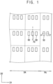
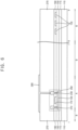
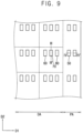
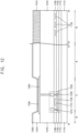
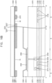
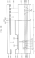
- FIG. 1 is a plan view illustrating an organic light emitting display device.
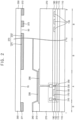
- FIG. 2 is a cross-sectional view taken along the line I-I' and the line II-II' of FIG. 1 .
- an organic light emitting display device includes a display area DA and a peripheral area PA.
- An organic light emitting display includes a light-emitting region A and a reflection region B. Pixels 60, 70 and 80 are positioned in the light-emitting region A.
- the pixel 60 may be a pixel emitting a red color
- the pixel 70 may be a pixel emitting a green color
- the pixel 80 may be a pixel emitting a blue color.
- a reflective member 370 is disposed in the reflection region B.
- the reflective member 370 includes a first reflective portion 371 disposed in the display area DA and a second reflective portion 372 disposed in the peripheral area PA.
- the first reflective portion 371 is integrally formed with the second reflective portion 372.
- the reflective member 370 may include a material having predetermined reflectivity.
- the reflective member 370 may include gold (Au), silver (Ag), aluminum (Al), magnesium (Mg), platinum (Pt), Nickel (Ni), titanium (Ti), etc.
- the reflective member 370 may be formed of an alloy, metal nitride, conductive metal oxide, etc.
- the reflective member 370 may include an alloy containing aluminum, aluminum nitride (AlNx), an alloy containing silver, tungsten nitride (WNx), an alloy containing copper, chrome nitride (CrNx), an alloy containing molybdenum, titanium nitride (TiNx), tantalum nitride (TaNx), strontium ruthenium oxide (SRO), zinc oxide (ZnOx), stannum (tin) oxide (SnOx), indium oxide (InOx), gallium oxide (GaOx), etc.
- the first reflective portion 371 has a plurality of first openings 60, 70 and 80.
- the second reflective portion 372 has a plurality of second openings.
- the first openings 60, 70 and 80 and the second openings 50 may have a quadrangular shape.
- the second openings 50 have a different shape and/or a different size from any of the first openings 60, 70 and 80 so that the reflectivity of the second reflective portion 372 is equal to the reflectivity of the first reflective portion 371.
- An organic light emitting display device includes 7a first substrate 110, a buffer layer 115, a first insulation interlayer 150, a second insulation layer 190, a third insulation layer 270, a light emitting structure, a pixel defining layer 310, a first sensing electrode 370, and a second substrate 350.
- the light emitting structure includes a switching element 250, a first electrode 290, an emission layer 330 and a second electrode 340.
- the switching element 250 includes an active pattern 130, a gate electrode 170, a source electrode 210 and a drain electrode 230.
- the reflective member 370 includes the first openings 60, 70 and 80 formed in the display area and the second openings 50 formed in the peripheral area.
- the organic light emitting display device 100 may include a plurality of pixel regions.
- One pixel region includes a light-emitting region A and a reflection region B.
- the reflection region B may substantially surround the light-emitting region A.
- the switching element 250, the first electrode 290, the emission layer 330 and a portion of the second electrode 340 may be disposed in the light-emitting region A. However, the switching element 250 may be disposed in the reflection region B.
- a display image is displayed in light-emitting region A.
- An image of an object that is located in the front of the organic light emitting display device 100 is reflected in the reflection region B.
- the light emitting structure is disposed on the first substrate 110.
- the first substrate 110 may be formed of transparent materials.
- the first substrate 110 may include quartz, synthetic quartz, calcium fluoride, fluoride-doped quartz, a soda lime glass, a non-alkali glass etc.
- the first substrate 110 may be formed of a flexible transparent resin substrate.
- the flexible transparent resin substrate for the first substrate 110 may include a polyimide substrate.
- the polyimide substrate may include a first polyimide layer, a barrier film layer, a second polyimide layer, etc.
- the polyimide substrate may be formed on a rigid glass substrate to help support the formation of the light emitting structure. That is, in embodiments, the first substrate 110 may have a structure in which the first polyimide layer, the barrier film layer and the second polyimide layer are stacked on a glass substrate.
- the light emitting structure e.g., the switching element 250, a capacitor, the first electrode 290, the light emitting layer 330, the second electrode 340, etc
- the insulation layer may be provided on the insulation layer.
- the glass substrate may be removed. It may be difficult for the light emitting structure to be directly formed on the polyimide substrate, because the polyimide substrate is thin and flexible. Accordingly, the light emitting structure is formed on a rigid glass substrate, and then the polyimide substrate may serve as the first substrate 110 after removal of the glass substrate. As the organic light emitting display device 100 includes the light-emitting region A and the reflection region B, the first substrate 110 may also include the light-emitting region A and the reflection region B.
- a buffer layer 115 may be disposed on the first substrate 110.
- the buffer layer 115 may extend from the light-emitting region A into the reflection region B.
- the buffer layer 115 may prevent the diffusion (e.g., an out-gassing) of metal atoms and/or impurities from the first substrate 110.
- the buffer layer 115 may control a rate of heat transfer in a crystallization process for forming the active pattern 130, thereby obtaining a substantially uniform active pattern 130.
- the buffer layer 115 may improve a surface flatness of the first substrate 110 when a surface of the first substrate 110 is relatively irregular. According to a type of the first substrate 110, at least two buffer layers may be provided on the first substrate 110, or the buffer layer may not be present.
- the switching element 250 may include the active pattern 130, the gate electrode 170, the source electrode 210, and the drain electrode 230.
- the active pattern 130 may be disposed on the first substrate 110.
- the active pattern 130 may be formed of an oxide semiconductor, an inorganic semiconductor (e.g., amorphous silicon, polysilicon, etc.), an organic semiconductor, etc.
- the first insulation layer 150 may be disposed on the active pattern 130.
- the first insulation layer 150 may cover the active pattern 130 in the light-emitting region A, and may extend in the first direction on the first substrate 110. That is, the first insulation layer 150 may be disposed on substantially the entire first substrate 110.
- the first insulation layer 150 may be formed of a silicon compound, a metal oxide, etc.
- the gate electrode 170 may be disposed on a portion of the first insulation layer 150 under which the active pattern 130 is disposed.
- the gate electrode 170 may be formed of a metal, an alloy, metal nitride, conductive metal oxide, transparent conductive materials, etc.
- the second insulation layer 190 may be disposed on the gate electrode 170.
- the second insulation layer 190 may cover the gate electrode 170 in the light-emitting region A, and may extend in the first direction on the first substrate 110. That is, the second insulation layer 190 may be disposed on substantially the entire first substrate 110.
- the second insulation layer 190 may be formed of a silicon compound, a metal oxide, etc.
- the source electrode 210 and the drain electrode 230 may be disposed on the second insulation layer 190.
- the source electrode 210 may be in contact with a first side of the active pattern 130 by removing a portion of the first and second insulation layers 150 and 190.
- the drain electrode 230 may be in contact with a second side of the active pattern 130 by removing a second portion of the first and second insulation layers 150 and 190.
- Each of the source electrode 210 and the drain electrode 230 may be formed of a metal, an alloy, metal nitride, conductive metal oxide, transparent conductive materials, etc.
- the third insulation layer 270 may be disposed on the source electrode 210 and the drain electrode 230.
- the third insulation layer 270 may cover the source electrode 210 and the drain electrode 230 in the sub-pixel region, and may extend in the first direction on the first substrate 110. That is, the third insulation layer 270 may be disposed on substantially the entire first substrate 110.
- the third insulation layer 270 may be formed of a silicon compound, a metal oxide, etc.
- the first electrode 290 may be disposed on the third insulation layer 270.
- the first electrode 290 may be in contact with the source electrode 210 by removing a portion of the third insulation layer 270. That is, the first electrode 290 may be electrically connected to the switching element 250.
- the first electrode 290 may be formed of a metal, an alloy, metal nitride, conductive metal oxide, transparent conductive materials, etc.
- the gate electrode 170 is disposed on the active pattern 130.
- the gate electrode 170 may instead be disposed under the active pattern 130.
- the pixel defining layer 310 may be disposed on the third insulation layer 270 to expose a portion of the first electrode 290.
- the pixel defining layer 310 may be formed of organic materials or inorganic materials.
- the light emitting layer 330 may be disposed on a portion of the first electrode 290 that is exposed by the pixel defining layer 310.
- the light emitting layer 330 is disposed on the exposed first electrode 290.
- the light emitting layer 330 is formed using light emitting materials capable of generating different colors of light (e.g., a red color, a blue color, and a green color).
- light emitting materials capable of generating different colors of light e.g., a red color, a blue color, and a green color.
- the present inventive concept is not limited thereto, and the light emitting layer 330 may instead stack light emitting materials capable of generating different colors of light, so as to emit white (or other) colored light.
- the second electrode 340 is disposed on the pixel defining layer 310 and the light emitting layer 330.
- the second electrode 340 may cover the pixel defining layer 310 and the light emitting layer 330 in the light-emitting region A and the reflection region B, and may extend in the first direction on the first substrate 110. That is, the second electrode 340 may be electrically connected to the first through third pixels.
- the second electrode 340 may be formed of a metal, an alloy, metal nitride, conductive metal oxide, a transparent conductive material, etc. These may be used alone or in any combination thereof.
- the first substrate 110 may be coupled to the second substrate 350 by using a sealing member.
- a filler may be disposed between the first substrate 110 and the second substrate 350.
- the reflective member 370 includes a material having predetermined reflectivity.
- the reflective member 370 may include gold (Au), silver (Ag), aluminum (Al), magnesium (Mg), platinum (Pt), Nickel (Ni), titanium (Ti), etc.
- the reflective member 370 may be formed of an alloy, metal nitride, conductive metal oxide, etc.
- the reflective member 370 may include an alloy containing aluminum, aluminum nitride (AlNx), an alloy containing silver, tungsten nitride (WNx), an alloy containing copper, chrome nitride (CrNx), an alloy containing molybdenum, titanium nitride (TiNx), tantalum nitride (TaNx), strontium ruthenium oxide (SRO), zinc oxide (ZnOx), stannum oxide (SnOx), indium oxide (InOx), gallium oxide (GaOx), etc.
- the second substrate 350 and the first substrate 110 may include substantially the same materials.
- the second substrate 350 may be formed of quartz, synthetic quartz, calcium fluoride, fluoride-doped quartz, soda lime glass, non-alkali glass, etc.
- the second substrate 350 may be formed of a transparent inorganic material or flexible plastic.
- the second substrate 350 may include a flexible transparent resin substrate.
- the second substrate 350 may include a stacked structure where at least one organic layer and at least one inorganic layer are alternately stacked.
- FIGS. 3 to 8 are cross-sectional views illustrating a method of manufacturing the organic light emitting display device of FIG. 2 .
- the buffer layer 115 is formed on the first substrate 110. Thereafter, the active pattern 130 and the first insulation layer 150 are formed on the buffer layer 115.
- the first substrate 110 may include quartz, synthetic quartz, calcium fluoride, fluoride-doped quartz, a soda lime glass, a non-alkali glass, etc.
- the first substrate 110 may be formed of transparent materials.
- the first substrate 110 may include quartz, synthetic quartz, calcium fluoride, fluoride-doped quartz, a soda lime glass, a non-alkali glass, etc.
- the first substrate 110 may be formed of a flexible transparent resin substrate.
- the flexible transparent resin substrate for the first substrate 110 may include a polyimide substrate.
- the polyimide substrate may include a first polyimide layer, a barrier film layer, a second polyimide layer, etc. When the polyimide substrate is thin and flexible, it may be formed on a rigid glass substrate to help support the formation of the light emitting structure.
- the first substrate 110 may have a structure in which the first polyimide layer, the barrier film layer and the second polyimide layer are stacked on a glass substrate.
- the light emitting structure e.g., the switching element 250, a capacitor, the first electrode 290, the light emitting layer 330, the second electrode 340, etc. may be disposed on the insulation layer.
- the glass substrate may be removed. It may be difficult that the light emitting structure is directly formed on the polyimide substrate because the polyimide substrate is thin and flexible. Accordingly, the light emitting structure may be formed on a rigid glass substrate, and then the polyimide substrate may serve as the first substrate 110 after the of the glass substrate. As the organic light emitting display device 100 includes the light-emitting region A and the reflection region B, the first substrate 110 also includes the light-emitting region A and the reflection region B.
- a buffer layer 115 may be disposed on the first substrate 110.
- the buffer layer 115 may extend from the light-emitting region A into the reflection region B.
- the buffer layer 115 may prevent the diffusion (e.g., out-gassing) of metal atoms and/or impurities from the first substrate 110.
- the buffer layer 115 may control a rate of heat transfer in a crystallization process for forming the active pattern 130, thereby obtaining a substantially uniform active pattern 130.
- the buffer layer 115 may improve a surface flatness of the first substrate 110 when a surface of the first substrate 110 is relatively irregular. According to a type of the first substrate 110, at least two buffer layers may be provided on the first substrate 110, or the buffer layer may not be present.
- the active pattern 130 may be formed of an oxide semiconductor, an inorganic semiconductor (e.g., amorphous silicon, polysilicon, etc.), an organic semiconductor, etc.
- the first insulation layer 150 may be disposed on the active pattern 130.
- the first insulation layer 150 may cover the active pattern 130 in the light-emitting region A, and may extend in the first direction on the first substrate 110. That is, the first insulation layer 150 may be disposed on substantially the entire first substrate 110.
- the first insulation layer 150 may be formed of a silicon compound, a metal oxide, etc.
- the gate electrode 170, a metal line 135 and the second insulation layer 190 are formed on the first substrate 110 after the first insulation layer 150 is formed.
- the gate electrode 170 may be disposed on a portion of the first insulation layer 150 under which the active pattern 130 is disposed.
- the gate electrode 170 may be formed of a metal, an alloy, metal nitride, conductive metal oxide, transparent conductive materials, etc.
- the metal line 135 may be disposed on the same layer as the gate electrode 170.
- the metal line 135 may include the same material as the gate electrode 170.
- the metal line 135 may be formed of a metal, an alloy, metal nitride, conductive metal oxide, transparent conductive materials, etc.
- the metal line 135 may be a line, a circuit or a common line electrically connected to the switching element 250.
- the present inventive concept is not limited thereto, and the metal line 135 may instead, for example, be disposed on the same layer as the source electrode 210 and the drain electrode 230.
- the second insulation layer 190 may be disposed on the gate electrode 170.
- the second insulation layer 190 may cover the gate electrode 170 in the light-emitting region A, and may extend in the first direction on the first substrate 110. That is, the second insulation layer 190 may be disposed on the entire first substrate 110.
- the second insulation layer 190 may be formed of a silicon compound, a metal oxide, etc.
- the source electrode 210 and the drain electrode 230 are formed on the first substrate 110 after the second insulation layer 190 is formed.
- the source electrode 210 and the drain electrode 230 may be disposed on the second insulation layer 190.
- the source electrode 210 may be in contact with a first side of the active layer 130 by removing a portion of the first and second insulation layers 150 and 190.
- the drain electrode 230 may be in contact with a second side of the active layer 130 by removing a second portion of the first and second insulation layers 150 and 190.
- Each of the source electrode 210 and the drain electrode 230 may be formed of a metal, an alloy, metal nitride, conductive metal oxide, transparent conductive materials, etc.
- the gate electrode 170 is disposed on the active pattern 130.
- the present inventive concept is not limited thereto, and the gate electrode 170 may instead, for example, be disposed under the active pattern 130.
- the third insulation layer 270 and the first electrode 290 are formed on the first substrate 110 over the source electrode 210 and the drain electrode 230.
- the third insulation layer 270 may be disposed on the source electrode 210 and the drain electrode 230.
- the third insulation layer 270 may cover the source electrode 210 and the drain electrode 230 in the sub-pixel region A, and may extend in the first direction on the first substrate 110. That is, the third insulation layer 270 may be disposed on substantially the entire first substrate 110.
- the third insulation layer 270 may be formed of a silicon compound, a metal oxide, etc.
- the first electrode 290 may be disposed on the third insulation layer 270.
- the first electrode 290 may be in contact with the source electrode 210 by removing a portion of the third insulation layer 270.
- the first electrode 290 may be electrically connected to the switching element 250.
- the first electrode 290 may be formed of a metal, an alloy, metal nitride, conductive metal oxide, transparent conductive materials, etc.
- the pixel defining layer 310, the light emitting layer 330 and the second electrode 340 are formed on the first substrate 110 over the first electrode 290.
- the pixel defining layer 310 may be disposed on the third insulation layer 270 to expose a portion of the first electrode 290.
- the pixel defining layer 310 may be formed of organic materials or inorganic materials.
- the light emitting layer 330 may be disposed on the portion of first electrode 290 that is exposed by the pixel defining layer 310.
- the light emitting layer 330 is disposed on the exposed first electrode 290.
- the light emitting layer 330 is formed using light emitting materials capable of generating different colors of light (e.g., a red color, a blue color, and a green color).
- light emitting materials capable of generating different colors of light e.g., a red color, a blue color, and a green color.
- the present inventive concept is not limited thereto, and the light emitting layer 330 may instead stack light emitting materials capable of generating different colors of light, so as to emit white or other colored light.
- the second electrode 340 may be disposed on the pixel defining layer 310 and the light emitting layer 330.
- the second electrode 340 may cover the pixel defining layer 310 and the light emitting layer 330 in the light-emitting region A and the reflection region B, and may extend in the first direction on the first substrate 110. That is, the second electrode 340 may be electrically connected to the first through third pixels 60, 70 and 80.
- the second electrode 340 may be formed of a metal, an alloy, metal nitride, conductive metal oxide, a transparent conductive material, etc. These may be used alone or in any combination thereof.
- the pixel defining layer 310 and the second electrode 340 may not be formed in (i.e. may be removed from) the peripheral area PA.
- the present inventive concept is not limited thereto, at least one of the pixel defining layer 310 and the second electrode 340 may be formed in the peripheral area PA or at least portion of the peripheral area PA.
- the reflective member 370 is formed on the second substrate 350.
- the second substrate 350 and the first substrate 110 may include substantially the same materials.
- the second substrate 350 may be formed of quartz, synthetic quartz, calcium fluoride, fluoride-doped quartz, soda lime glass, non-alkali glass, etc.
- the reflective member 370 includes a first reflective portion 371 disposed in the display area DA, and a second reflective portion 372 disposed in the peripheral area PA.
- the first reflective portion 371 is integrally formed with the second reflective portion 372.
- the reflective member 370 may include an alloy containing aluminum, aluminum nitride (AlNx), an alloy containing silver, tungsten nitride (WNx), an alloy containing copper, chrome nitride (CrNx), an alloy containing molybdenum, titanium nitride (TiNx), tantalum nitride (TaNx), strontium ruthenium oxide (SRO), zinc oxide (ZnOx), stannum oxide (SnOx), indium oxide (InOx), gallium oxide (GaOx), etc.
- the first reflective portion 371 has a plurality of first openings 60, 70 and 80.
- the second reflective portion 372 has a plurality of second openings 50
- the first openings 60, 70 and 80 and the second openings 50 may have a quadrangular shape.
- the second openings 50 have a different shape and/or a different size from the first openings 60, 70 and 80 so that the reflectivity of the second reflective portion 372 is equal to the reflectivity of the first reflective portion 371.
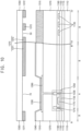
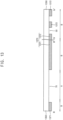
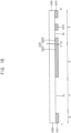
- FIG. 9 is a plan view illustrating an organic light emitting display device.
- FIG. 10 is a cross-sectional view taken along the line III-III' and the line IV-IV' of FIG. 9 .
- the light-blocking pattern 1315 overlaps the metal line 1135.
- the light-blocking pattern 1315 may be disposed on the same layer as the pixel defining layer 1310.
- the reflective member 1370 includes a first reflective portion 1371 disposed in the display area DA and a second reflective portion 1372 disposed in the peripheral area PA.
- the first reflective portion 1371 is integrally formed with the second reflective portion 1372.
- the first reflective portion 1371 has a plurality of first openings 60, 70 and 80.
- the second reflective portion 1372 has a plurality of second openings 50
- the first openings 60, 70 and 80 and the second openings 50 may have a generally quadrangular shape.
- the second openings 50 have a different shape and a different size from the first openings 60, 70 and 80 so that the reflectivity of the second reflective portion 1372 is equal to the reflectivity of the first reflective portion 1371.
- the light-blocking pattern 1315 overlaps the metal line 1135, and thus the light-blocking pattern 1315 may block light due to reflection from the metal line 1135. Since light from a lower substrate is blocked, a reflectivity of the reflective member 1370 may be constant. Thus, a reflectivity of the second reflective portion 1372 is adjusted by adjusting of a shape and a size of the second openings 50. The reflectivity of the second reflective portion 1372 is the same as a reflectivity of the first reflective portion 1371.
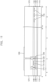
- FIGS. 11 to 13 are cross-sectional views illustrating a method of manufacturing the organic light emitting display device of FIG. 10 .
- the third insulation layer 1270 and the first electrode 1290 are formed on the first substrate 1110 on which the source electrode 1210 and the drain electrode 1230 are formed.
- the third insulation layer 1270 may be disposed on the source electrode 1210 and the drain electrode 1230.
- the third insulation layer 1270 may cover the source electrode 1210 and the drain electrode 1230 in the sub-pixel region A, and may extend in the first direction on the first substrate 1110. That is, the third insulation layer 1270 may be disposed on the entire first substrate 1110.
- the third insulation layer 1270 may be formed of a silicon compound, a metal oxide, etc.
- the first electrode 1290 may be disposed on the third insulation layer 1270.
- the first electrode 1290 may be in contact with the source electrode 1210 by removing a portion of the third insulation layer 1270. In this manner, the first electrode 1290 may be electrically connected to the switching element 1250.
- the first electrode 1290 may be formed of a metal, an alloy, metal nitride, conductive metal oxide, transparent conductive materials, etc.
- the pixel defining layer 1310, the light-blocking pattern 1315, the light emitting layer 1330 and the second electrode 1340 are formed on the first substrate 1110 on which the first electrode 1290 is formed.
- the pixel defining layer 1310 may be disposed on the third insulation layer 1270 to expose a portion of the first electrode 1290.
- the pixel defining layer 1310 may be formed of organic materials or inorganic materials.
- the light emitting layer 1330 may be disposed on a portion that the first electrode 1290 is exposed by the pixel defining layer 1310.
- the light-blocking pattern 1315 may include an opaque material.
- the light-blocking pattern 1315 may include a black organic material.
- the light-blocking pattern 1315 may include a carbon or a cobalt. Therefore, the light-blocking pattern 1315 may block light due to reflection by metal wirings.
- the light emitting layer 1330 may be disposed on the exposed first electrode 1290.
- the light emitting layer 1330 may be formed using light emitting materials capable of generating different colors of light (e.g., a red color, a blue color, and a green color). However, the light emitting layer 1330 may stack light emitting materials capable of generating different colors of light, so as to emit white or other colored light.
- the second electrode 1340 may be disposed on the pixel defining layer 1310 and the light emitting layer 1330.
- the second electrode 1340 may cover the pixel defining layer 1310 and the light emitting layer 1330 in the light-emitting region A and the reflection region B, and may extend in the first direction on the first substrate 1110. That is, the second electrode 1340 may be electrically connected to the first through third pixels.
- the second electrode 1340 may be formed of a metal, an alloy, metal nitride, conductive metal oxide, a transparent conductive material, etc. These may be used alone or in any combination thereof.
- the reflective member 1370 is formed on the second substrate 1350.
- the second substrate 1350 and the first substrate 1110 may include substantially the same materials.
- the second substrate 1350 may be formed of quartz, synthetic quartz, calcium fluoride, fluoride-doped quartz, soda lime glass, non-alkali glass, etc.
- the reflective member 1370 includes a first reflective portion 1371 disposed in the display area DA, and a second reflective portion 1372 disposed in the peripheral area PA.
- the first reflective portion 1371 is integrally formed with the second reflective portion 1372.
- the reflective member 1370 may include a material having predetermined reflectivity.
- the reflective member 1370 may include gold (Au), silver (Ag), aluminum (Al), magnesium (Mg), platinum (Pt), Nickel (Ni), titanium (Ti), etc.
- the reflective member 1370 may be formed of an alloy, metal nitride, conductive metal oxide, etc.
- the reflective member 1370 may include an alloy containing aluminum, aluminum nitride (AlNx), an alloy containing silver, tungsten nitride (WNx), an alloy containing copper, chrome nitride (CrNx), an alloy containing molybdenum, titanium nitride (TiNx), tantalum nitride (TaNx), strontium ruthenium oxide (SRO), zinc oxide (ZnOx), stannum oxide (SnOx), indium oxide (InOx), gallium oxide (GaOx), etc.
- the first reflective portion 1371 has a plurality of first openings 60, 70 and 80.
- the second reflective portion 1372 may have a plurality of second openings 50.
- the first openings 60, 70 and 80 and the second openings 50 may have a generally quadrangular shape.
- the second openings 50 have a different shape and a different size from the first openings 60, 70 and 80 so that the reflectivity of the second reflective portion 1372 is equal to the reflectivity of the first reflective portion 1371.
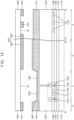
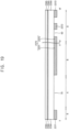
- FIG. 14 is a cross-sectional view taken along the line III-III' and the line IV-IV' of FIG. 9 .
- the organic light emitting display device is substantially the same as the organic light emitting display device of FIG. 10 except for a pixel defining layer 1310, and thus same reference numerals are used for same elements and repetitive explanation will be omitted.
- an organic light emitting display device may include a light-blocking pattern 1315 integrally formed with pixel defining layer 1310.
- the light-blocking pattern 1315 overlaps the metal line 1135.
- the light-blocking pattern 1315 may be disposed on the same layer as the pixel defining layer 1310.
- the pixel defining layer 1310 may include an opaque material.
- the pixel defining layer 1310 may include a black organic material.
- the pixel defining layer 1310 may include a carbon or a cobalt.
- the light-blocking pattern 1315 may be formed from the same material as pixel defining layer 1310, which may include an opaque material.
- the light-blocking pattern 1315 may include a black organic material.
- the light-blocking pattern 1315 may include a carbon or a cobalt. Therefore, the light-blocking pattern 1315 may block light due to reflection by metal wirings.
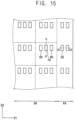
- FIG. 15 is a plan view illustrating an organic light emitting display device according to an embodiment.
- FIG. 16A , 16B and 16C are cross-sectional views taken along the line V-V' and the line VI-VI' of FIG. 15 .
- the organic light emitting display device is substantially the same as the organic light emitting display device of FIGS. 1 and 2 , except for a first reflective member 2370 and a second reflective member 2390.
- an organic light emitting display device may include a first reflective member 2370 and a second reflective member 2390.
- a reflective member device includes a first reflective member 2370 disposed in the reflection region B, and a second reflective member 2390 disposed in the light-emitting region A and the reflection region B.
- a reflectivity of the first reflective member 2370 may be different from a reflectivity of the second reflective member 2390.
- a thickness of the second reflective member 2390 may be thinner than a thickness of the first reflective member 2370.
- a portion of light may penetrate through the second reflective member 2390 and a portion of light may be reflected by the second reflective member 2390.
- scattered reflection may occur at an edge of the first reflective member 2370.
- an organic light emitting display device includes the second reflective member 2390 disposed in the light-emitting region A and the reflection region B. Thus, scattered reflection from edges of the first reflection member may be decreased.
- the first reflective member 2370 may be disposed on a first (e.g., lower) surface of the second substrate 2350, and the second reflective member 2390 may be disposed on a second (e.g., upper) surface opposing the first surface of the second substrate 2350.
- the first reflective member 2370 may be disposed under the second substrate 2350, and the second reflective member 2390 may be disposed above the second substrate 2350.
- a fourth insulation layer 2395 may be disposed on the second reflective member 2390.
- both the first reflective member 2370 and the second reflective member 2390 may be disposed on the first (e.g., lower) surface of the second substrate 2350.
- the first reflective member 2370 may be disposed under the second substrate 2350
- the second reflective member 2390 may be disposed between the second substrate 2350 and the first reflective member 2370.
- both the first reflective member 2370 and the second reflective member 2390 may be disposed on the first (e.g., lower) surface of the second substrate 2350.
- the second reflective member 2390 may be disposed under the second substrate 2350, and the first reflective member 2370 may be disposed between the second substrate 2350 and the second reflective member 2390.
- FIGS. 17 to 19 are cross-sectional views illustrating a method of manufacturing the organic light emitting display device of FIG. 16A .
- the pixel defining layer 2310, the light emitting layer 2330 and the second electrode 2340 are formed on the first substrate 2110 on which the first electrode 2290 is formed.
- the method of manufacturing an organic light emitting display device is substantially the same as the method of manufacturing an organic light emitting display device of FIGS. 3 to 7 , and thus same reference numerals are used for same elements and repetitive explanation will be omitted.
- the first reflective member 2370 is formed on a first surface of the second substrate 2350.
- the second substrate 2350 and the first substrate 2110 may include substantially the same materials.
- the second substrate 2350 may be formed of quartz, synthetic quartz, calcium fluoride, fluoride-doped quartz, soda lime glass, non-alkali glass etc.
- the first reflective member 2370 may include a first reflective portion 2371 disposed in the display area DA, and a second reflective portion 2372 disposed in the peripheral area PA.
- the first reflective portion 2371 may be integrally formed with the second reflective portion 2372.
- the second reflective member 2390 is formed on a second (upper) surface opposing the first (lower) surface of the second substrate 2350.
- the fourth insulation layer 2395 is formed on the second reflective member 2390.
- the second reflective member 2390 is formed directly on the second surface opposing the first surface of the second substrate 2350.
- the second reflective member 2390 is disposed in the light-emitting region A and the reflection region B.
- an insulation layer may instead be disposed between the second substrate 2350 and the second reflective member 2390, for example.
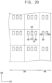
- FIG. 20 is a plan view illustrating an organic light emitting display device according to an embodiment.
- FIG. 21 is a cross-sectional view taken along the line VII-VII' and the line VIII-VIII' of FIG. 20 .
- the organic light emitting display device is substantially the same as the organic light emitting display device of FIGS. 1 and 2 , except for a thin film encapsulation layer 3410 and a fourth insulation layer 3420. Thus, same reference numerals are used for same elements and repetitive explanation will be omitted.
- an organic light emitting display may include the thin film encapsulation layer 3410 formed on a second electrode 3340, and the fourth insulation layer 3420 formed on a reflective member 3370.
- the thin film encapsulation layer 3410 may include at least one inorganic layer and at least one organic layer.
- the thin film encapsulation layer 3410 may be formed by stacking (e.g., sequentially stacking) a first inorganic layer, an organic layer, and a second inorganic layer.
- the organic layer may be formed of a polymer, and may itself be a single layer or multiple layers (e.g., stacked layers) that is formed of, for example, one of polyethylene terephthalate, a polyimide, a polycarbonate, an epoxy, a polyethylene and a polyacrylate.
- the organic layer may also be formed of a polyacrylate; for example, the organic layer may include a polymerized monomer composition including a diacrylate monomer or a triacrylate monomer.
- the monomer composition may further include a monoacrylate monomer.
- the monomer composition may further include a suitable photoinitiator such as thermoplastic polyolefin (TPO), but is not limited thereto.
- TPO thermoplastic polyolefin
- the first inorganic layer and the second inorganic layer may be single layers or stacked layers including a metal oxide or a metal nitride.
- the first inorganic layer and the second inorganic layer may include one of silicon nitride (e.g., SiNx), aluminum oxide (e.g., Al2O3), silicon oxide (e.g., SiO2), and titanium oxide (e.g., TiO2).
- the second inorganic layer may be formed to or configured to prevent or reduce moisture from permeating into the light-emitting structure.
- the thin film encapsulation layer 3410 may be formed by stacking (e.g., sequentially stacking) a first inorganic layer, a first organic layer, a second inorganic layer, a second organic layer and a third inorganic layer.
- the reflective member 3370 is formed on the thin film encapsulation layer 3410.
- the reflective member 3370 includes a first reflective portion 3371 disposed in the display area DA, and a second reflective portion 3372 disposed in the peripheral area PA.
- the first reflective portion 3371 is integrally formed with the second reflective portion 3372.
- the reflective member 3370 may include an alloy containing aluminum, aluminum nitride (AlNx), an alloy containing silver, tungsten nitride (WNx), an alloy containing copper, chrome nitride (CrNx), an alloy containing molybdenum, titanium nitride (TiNx), tantalum nitride (TaNx), strontium ruthenium oxide (SRO), zinc oxide (ZnOx), stannum oxide (SnOx), indium oxide (InOx), gallium oxide (GaOx), etc.
- the first reflective portion 3371 has a plurality of first openings 60, 70 and 80.
- the second reflective portion 3372 has a plurality of second openings 50.
- the first openings 60, 70 and 80 and the second openings 50 may, for example, generally have a quadrangular shape.
- the second openings 50 have a different shape and a different size from the first openings 60, 70 and 80 so that the reflectivity of the second reflective portion 3372 is equal to the reflectivity of the first reflective portion 3371.
- a fourth insulation layer 3420 may be disposed on the reflective member 3370.
- the fourth insulation layer 3420 may be formed of a silicon compound, a metal oxide, etc.
- FIG. 22 is a cross-sectional view taken along the line VII-VII' and the line VIII-VIII' of FIG. 20 .
- the organic light emitting display device is substantially the same as the organic light emitting display of FIG. 21 except for a first reflective member 3370 and a second reflective member 3390, and thus same reference numerals are used for same elements and repetitive explanation will be omitted.
- a reflective member may include a first reflective member 3370 disposed in the reflection region B, and a second reflective member 3390 disposed in the light-emitting region A and the reflection region B.
- the first reflective member 3370 is formed on the thin film encapsulation layer 3410.
- the second reflective member 3390 is disposed on the film encapsulation layer 3410 over the first reflective member 3370.
- a reflectivity of the first reflective member 3370 may be different from a reflectivity of the second reflective member 3390.
- a thickness of the second reflective member 3390 may be thinner than a thickness of the first reflective member 3370.
- a portion of light may penetrate through the second reflective member 3390 and a portion of light may be reflected by the second reflective member 3390.
- scattered reflection may occur at an edge of the first reflective member 3370.
- an organic light emitting display device includes the second reflective member 3390 disposed in the light-emitting region A and the reflection region B. Thus, scattered reflection occurring at an edge of the first reflection member may be decreased.
- FIG. 23 is a cross-sectional view taken along the line VII-VII' and the line VIII-VIII' of FIG. 20 .
- the organic light emitting display device is substantially the same as the organic light emitting display device of FIG. 21 except for a first reflective member 3370 and a second reflective member 3390, and thus same reference numerals are used for same elements and repetitive explanation will be omitted.
- a reflective member may include a first reflective member 3370 disposed in the reflection region B, and a second reflective member 3390 disposed in the light-emitting region A and the reflection region B.
- the second reflective member 3390 is formed on the thin film encapsulation layer 3410.
- the first reflective member 3370 is disposed on the second reflective member 3390.
- a reflectivity of the first reflective member 3370 may be different from a reflectivity of the second reflective member 3390.
- a thickness of the second reflective member 3390 may be thinner than a thickness of the first reflective member 3370.
- a portion of light may penetrate through the second reflective member 3390 and a portion of light may be reflected by the second reflective member 3390.
- scattered reflection may occur at an edge of the first reflective member 3370.
- an organic light emitting display device includes the second reflective member 3390 disposed in the light-emitting region A and the reflection region B. Thus, scattered reflection occurring at an edge of the first reflection member may be decreased.
- FIGS. 24 to 26 are cross-sectional views illustrating a method of manufacturing the organic light emitting display device of FIG. 21 .
- the pixel defining layer 3310, the light emitting layer 3330 and the second electrode 3340 are formed on the first substrate 3110 on which the first electrode 3290 is formed.
- the method of manufacturing an organic light emitting display is substantially the same as the method of manufacturing an organic light emitting display device of FIGS. 3 to 7 , and thus same reference numerals are used for same elements and repetitive explanation will be omitted.
- the thin film encapsulation layer 3410 is formed on the first substrate 3110 on which the second electrode 3340 is formed.
- the thin film encapsulation layer 3410 may be formed by stacking (e.g., sequentially stacking) a first inorganic layer, an organic layer, and a second inorganic layer.
- the organic layer may be formed of a polymer, and may also be a single layer or multiple layers (e.g., stacked layers) that is formed of, e.g., one of polyethylene terephthalate, a polyimide, a polycarbonate, an epoxy, a polyethylene and a polyacrylate.
- the organic layer may also be formed of a polyacrylate; for example, the organic layer may include a polymerized monomer composition including a diacrylate monomer or a triacrylate monomer.
- the monomer composition may further include a monoacrylate monomer.
- the monomer composition may further include a suitable photoinitiator such as thermoplastic polyolefin (TPO), but is not limited thereto.
- TPO thermoplastic polyolefin
- the first inorganic layer and the second inorganic layer may be single layers or stacked layers including a metal oxide or a metal nitride.
- the first inorganic layer and the second inorganic layer may include one of silicon nitride (e.g., SiNx), aluminum oxide (e.g., Al2O3), silicon oxide (e.g., SiO2), and titanium oxide (e.g., TiO2).
- the second inorganic layer may be formed to or configured to prevent or reduce moisture from permeating into the light-emitting structure.
- the reflective member 3370 is formed on the first substrate 3110 on which the thin film encapsulation layer 3410 is formed.
- the reflective member 3370 includes a first reflective portion 3371 disposed in the display area DA and a second reflective portion 3372 disposed in the peripheral area PA.
- the first reflective portion 3371 is integrally formed with the second reflective portion 3372.
- the fourth insulation layer 3420 is formed on the first substrate 3110 on which the reflective member 3370 is formed.
- a fourth insulation layer 3420 may be disposed on the reflective member 3370.
- the fourth insulation layer 3420 may be formed of a silicon compound, a metal oxide, etc.
- FIG. 27 is a plan view illustrating an organic light emitting display.
- FIG. 28 is a cross-sectional view taken along the line IX-IX' and the line X-X' of FIG. 27 .
- the organic light emitting display is substantially the same as the organic light emitting display device of FIGS. 1 and 2 except for a light-blocking pattern 4315, a thin film encapsulation layer 4410 and a fourth insulation layer 4420, and thus same reference numerals are used for same elements and repetitive explanation will not be omitted.
- an organic light emitting display may include the light-blocking pattern 4315, the thin film encapsulation layer 4410 formed on a second electrode 4340 and the light-blocking pattern 4315, and the fourth insulation layer 4420 formed on a reflective member 4370.
- the light-blocking pattern 4315 overlaps the metal line 4135.
- the light-blocking pattern 4315 may be disposed on the same layer as the pixel defining layer 4310.
- the light-blocking pattern 4315 may include an opaque material.
- the light-blocking pattern 4315 may include a black organic material.
- the light-blocking pattern 4315 may include a carbon or a cobalt. Therefore, the light-blocking pattern 4315 may block light due to reflection by metal wirings such as the underlying metal line 4135.
- the thin film encapsulation layer 4410 may be formed by stacking (e.g., sequentially stacking) a first inorganic layer, an organic layer, and a second inorganic layer.
- the organic layer may be formed of a polymer, and may also be a single layer or multiple layers (e.g., stacked layers) that is formed of, for example, one of polyethylene terephthalate, a polyimide, a polycarbonate, an epoxy, a polyethylene and a polyacrylate.
- the organic layer may also be formed of a polyacrylate; for example, the organic layer may include a polymerized monomer composition including a diacrylate monomer or a triacrylate monomer.
- the monomer composition may further include a monoacrylate monomer.
- the monomer composition may further include a suitable photoinitiator such as thermoplastic polyolefin (TPO), but is not limited thereto.
- TPO thermoplastic polyolefin
- the first inorganic layer and the second inorganic layer may be single layers or stacked layers including a metal oxide or a metal nitride.
- the first inorganic layer and the second inorganic layer may include one of silicon nitride (e.g., SiNx), aluminum oxide (e.g., Al2O3), silicon oxide (e.g., SiO2), and titanium oxide (e.g., TiO2).
- the second inorganic layer may be formed to or configured to prevent or reduce permeation of moisture into the light-emitting structure.
- the thin film encapsulation layer 4410 may instead be formed by stacking (e.g., sequentially stacking) a first inorganic layer, a first organic layer, a second inorganic layer, a second organic layer and a third inorganic layer.
- the reflective member 4370 is formed on the thin film encapsulation layer 4410.
- a fourth insulation layer 4420 may be disposed on the reflective member 4370.
- the fourth insulation layer 4420 may be formed of a silicon compound, a metal oxide, etc.
- FIGS. 29 to 31 are cross-sectional views illustrating a method of manufacturing the organic light emitting display device of FIG. 28 .
- the pixel defining layer 4310, the light-blocking pattern 4315, the light emitting layer 4330 and the second electrode 4340 are formed on the first substrate 4110 on which the first electrode 4290 is formed.
- the method of manufacturing an organic light emitting display is substantially the same as the method of manufacturing an organic light emitting display device of FIGS. 3 to 7 , and thus same reference numerals are used for same elements and repetitive explanation will not be omitted.
- the light-blocking pattern 4315 overlaps the metal line 4135.
- the light-blocking pattern 4315 may be disposed on the same layer as the pixel defining layer 4310.
- the light-blocking pattern 4315 may include an opaque material.
- the light-blocking pattern 4315 may include a black organic material.
- the light-blocking pattern 4315 may include a carbon or a cobalt. Therefore, the light-blocking pattern 4315 may block light due to reflection by metal wirings.
- the thin film encapsulation layer 4410 is formed on the first substrate 4110 on which the second electrode 4340 is formed.
- the thin film encapsulation layer 4410 may be formed by stacking (e.g., sequentially stacking) a first inorganic layer, an organic layer, and a second inorganic layer.
- the organic layer may be formed of a polymer, and may also be a single layer or multiple layers (e.g., stacked layers) that is formed of, for example, one of polyethylene terephthalate, a polyimide, a polycarbonate, an epoxy, a polyethylene and a polyacrylate.
- the organic layer may also be formed of a polyacrylate; for example, the organic layer may include a polymerized monomer composition including a diacrylate monomer or a triacrylate monomer.
- the monomer composition may further include a monoacrylate monomer.
- the monomer composition may further include a suitable photoinitiator such as thermoplastic polyolefin (TPO), but is not limited thereto.
- TPO thermoplastic polyolefin
- the first inorganic layer and the second inorganic layer may be single layers or stacked layers including a metal oxide or a metal nitride.
- the first inorganic layer and the second inorganic layer may include one of silicon nitride (e.g., SiNx), aluminum oxide (e.g., Al2O3), silicon oxide (e.g., SiO2), and titanium oxide (e.g., TiO2).
- the second inorganic layer may be formed to or configured to prevent or reduce permeation of moisture into the light-emitting structure.
- the reflective member 4370 is formed on the first substrate 4110 on which the thin film encapsulation layer 4410 is formed.
- the reflective member 4370 includes a first reflective portion 4371 disposed in the display area DA and a second reflective portion 4372 disposed in the peripheral area PA.
- the first reflective portion 4371 is integrally formed with the second reflective portion 4372.
- the fourth insulation layer 4420 is formed on the first substrate 4110 on which the reflective member 4370 is formed.
- the fourth insulation layer 4420 may be disposed on the reflective member 4370.
- the fourth insulation layer 4420 may be formed of a silicon compound, a metal oxide, etc.
- FIG. 32 is a plan view illustrating an organic light emitting display device according to an exemplary embodiment of the inventive concept.
- FIG. 33 is a cross-sectional view taken along the line XI-XI' and the line XII-XII' of FIG. 27 .
- the organic light emitting display device is substantially the same as the organic light emitting display device of FIGS. 1 and 2 except for second openings 50 and a sealing member 5400, and thus same reference numerals are used for same elements and repetitive explanation will be omitted.
- an organic light emitting display device may include a sealing member 5400 coupling a first substrate 5110 and a second substrate 5350 together.
- the sealing member 5400 is disposed in the peripheral area PA between the first substrate 5110 and the second substrate 5350.
- the sealing member 5400 may encapsulate the display area DA.
- the second openings 50 may be formed in the peripheral area PA.
- the second openings 50 may be formed in an area between the sealing member 5400 and the display area DA, and an area between the sealing member 5400 and ends of the first and second substrates 5110 and 5350.
- the second openings 50 may overlap the sealing member 5400.
Landscapes
- Physics & Mathematics (AREA)
- Optics & Photonics (AREA)
- Engineering & Computer Science (AREA)
- Microelectronics & Electronic Packaging (AREA)
- Manufacturing & Machinery (AREA)
- Electroluminescent Light Sources (AREA)
- Geometry (AREA)
Description
- The present invention relates to organic light emitting display devices. More specifically, exemplary embodiments of the present inventive concept relate to organic light emitting display devices having improved reflective properties, and their manufacture.
- Flat panel display (FPD) devices have found wide use in various electronic devices, because the flat panel display device is lightweight and thin as compared to a cathode-ray tube (CRT) display device. Typical examples of a flat panel display device are a liquid crystal display (LCD) device and an organic light emitting diode (OLED) display device. Compared to the LCD, the OLED has many advantages such as a higher luminance and a wider viewing angle. In addition, the OLED display device can be made thinner because the OLED display device does not require a backlight. In the OLED display device, electrons and holes are injected into an organic thin layer through a cathode and an anode, and then recombined in the organic thin layer to generate excitons, thereby generating light of a certain wavelength.
- Recently, a mirror OLED device capable of reflecting an image of an object (or target) that is located in the front of the OLED device by including a reflective member has been developed. In addition, an OLED device having a mirror function and a touch function has been developed. The reflective member may be disposed in a display area and a peripheral area surrounding the display area.
- However, a reflectivity of a reflective member disposed in the display area may be different from a reflectivity of a reflective member disposed in the peripheral area. Thus, the reflective member disposed in the peripheral area may be seen as separate from the reflective member disposed in the display area.
-
US 2016/0043349 discloses an organic light emitting display device which includes a substrate, a light emitting structure, and a reflective metal layer. -
US 2015/002953 A1 relates to a mirror type display apparatus. -
US 2014/312321 A1 relates to an organic light emitting display device capable of taking photographs using external light without any image displayed on the screen. -
EP 0940796 A1 relates to an active matrix display device. -
US 9136315 B1 -
US 2009/009070 A1 relates to an organic light-emitting device for resolving the broken electrode issue and increasing the light-emitting area. -
US 2013/099660 A1 relates to an OLED, which can provide a function of a mirror and has good display brightness. -
Us 2015/034918 A1 relates to an organic light-emitting display apparatus that may realize a mirror function and a touch sensing function while not deteriorating display quality and efficiency. - According to an aspect of the invention, there is provided an organic light emitting display device as set out in
claim 1. - According to another aspect of the invention, there is provided a method of manufacturing an organic light emitting display device as set out in claim 6.
- Preferred embodiments are defined in the dependent claims.
-
FIG. 1 is a plan view illustrating an organic light emitting display device; -
FIG. 2 is a cross-sectional view taken along the line I-I' and the line II-II' ofFIG. 1 ; -
FIGS. 3 to 8 are cross-sectional views illustrating a method of manufacturing the organic light emitting display device ofFIG. 2 ; -
FIG. 9 is a plan view illustrating an organic light emitting display device; -
FIG. 10 is a cross-sectional view taken along the line III-III' and the line IV-IV' ofFIG. 9 ; -
FIGS. 11 to 13 are cross-sectional views illustrating a method of manufacturing the organic light emitting display device ofFIG. 10 ; -
FIG. 14 is a cross-sectional view taken along the line III-III' and the line IV-IV' ofFIG. 9 ; -
FIG. 15 is a plan view illustrating an organic light emitting display; -
FIG. 16A ,16B and16C are cross-sectional views taken along the line V-V' and the line VI-VI' ofFIG. 15 ; -
FIGS. 17 to 19 are cross-sectional views illustrating a method of manufacturing the organic light emitting display device ofFIG. 16A ; -
FIG. 20 is a plan view illustrating an organic light emitting display device; -
FIG. 21 is a cross-sectional view taken along the line VII-VII' and the line VIII-VIII' ofFIG. 20 ; -
FIG. 22 is a cross-sectional view taken along the line VII-VII' and the line VIII-VIII' ofFIG. 20 ; -
FIG. 23 is a cross-sectional view taken along the line VII-VII' and the line VIII-VIII' ofFIG. 20 ; -
FIGS. 24 to 26 are cross-sectional views illustrating a method of manufacturing the organic light emitting display device ofFIG. 21 ; -
FIG. 27 is a plan view illustrating an organic light emitting display; -
FIG. 28 is a cross-sectional view taken along the line IX-IX' and the line X-X' ofFIG. 27 ; -
FIGS. 29 to 31 are cross-sectional views illustrating a method of manufacturing the organic light emitting display device ofFIG. 28 ; -
FIG. 32 is a plan view illustrating an organic light emitting display device; and -
FIG. 33 is a cross-sectional view taken along the line XI-XI' and the line XII-XII' ofFIG. 27 . - Hereinafter, the present inventive concept will be explained in detail with reference to the accompanying drawings. The various Figures are not necessarily to scale. All numerical values are approximate, and may vary. All examples of specific materials and compositions are to be taken as non-limiting and exemplary only. Other suitable materials and compositions may be used instead.
-
FIG. 1 is a plan view illustrating an organic light emitting display device.FIG. 2 is a cross-sectional view taken along the line I-I' and the line II-II' ofFIG. 1 . - Referring to
FIGS. 1 and2 , an organic light emitting display device includes a display area DA and a peripheral area PA. - An organic light emitting display includes a light-emitting region A and a reflection
region B. Pixels pixel 60 may be a pixel emitting a red color, thepixel 70 may be a pixel emitting a green color, and thepixel 80 may be a pixel emitting a blue color. - A
reflective member 370 is disposed in the reflection region B. Thereflective member 370 includes a firstreflective portion 371 disposed in the display area DA and a secondreflective portion 372 disposed in the peripheral area PA. The firstreflective portion 371 is integrally formed with the secondreflective portion 372. - The
reflective member 370 may include a material having predetermined reflectivity. For example, thereflective member 370 may include gold (Au), silver (Ag), aluminum (Al), magnesium (Mg), platinum (Pt), Nickel (Ni), titanium (Ti), etc. Alternatively, thereflective member 370 may be formed of an alloy, metal nitride, conductive metal oxide, etc. For example, thereflective member 370 may include an alloy containing aluminum, aluminum nitride (AlNx), an alloy containing silver, tungsten nitride (WNx), an alloy containing copper, chrome nitride (CrNx), an alloy containing molybdenum, titanium nitride (TiNx), tantalum nitride (TaNx), strontium ruthenium oxide (SRO), zinc oxide (ZnOx), stannum (tin) oxide (SnOx), indium oxide (InOx), gallium oxide (GaOx), etc. - The first
reflective portion 371 has a plurality offirst openings reflective portion 372 has a plurality of second openings. Thefirst openings second openings 50 may have a quadrangular shape. In the inventive organic light emitting device having a mirror function, thesecond openings 50 have a different shape and/or a different size from any of thefirst openings reflective portion 372 is equal to the reflectivity of the firstreflective portion 371. - An organic light emitting display device according to an embodiment includes 7a
first substrate 110, abuffer layer 115, afirst insulation interlayer 150, asecond insulation layer 190, athird insulation layer 270, a light emitting structure, apixel defining layer 310, afirst sensing electrode 370, and asecond substrate 350. Here, the light emitting structure includes aswitching element 250, afirst electrode 290, anemission layer 330 and asecond electrode 340. The switchingelement 250 includes anactive pattern 130, agate electrode 170, asource electrode 210 and adrain electrode 230. Thereflective member 370 includes thefirst openings second openings 50 formed in the peripheral area. - The organic light emitting display device 100 may include a plurality of pixel regions. One pixel region includes a light-emitting region A and a reflection region B. The reflection region B may substantially surround the light-emitting region A. The switching
element 250, thefirst electrode 290, theemission layer 330 and a portion of thesecond electrode 340 may be disposed in the light-emitting region A. However, the switchingelement 250 may be disposed in the reflection region B. - A display image is displayed in light-emitting region A. An image of an object that is located in the front of the organic light emitting display device 100 is reflected in the reflection region B.
- The light emitting structure is disposed on the
first substrate 110. Thefirst substrate 110 may be formed of transparent materials. For example, thefirst substrate 110 may include quartz, synthetic quartz, calcium fluoride, fluoride-doped quartz, a soda lime glass, a non-alkali glass etc. Alternatively, thefirst substrate 110 may be formed of a flexible transparent resin substrate. Here, the flexible transparent resin substrate for thefirst substrate 110 may include a polyimide substrate. For example, the polyimide substrate may include a first polyimide layer, a barrier film layer, a second polyimide layer, etc. - When the polyimide substrate is thin and flexible, the polyimide substrate may be formed on a rigid glass substrate to help support the formation of the light emitting structure. That is, in embodiments, the
first substrate 110 may have a structure in which the first polyimide layer, the barrier film layer and the second polyimide layer are stacked on a glass substrate. Here, after an insulation layer is provided on the second polyimide layer, the light emitting structure (e.g., the switchingelement 250, a capacitor, thefirst electrode 290, thelight emitting layer 330, thesecond electrode 340, etc) may be disposed on the insulation layer. - After the light emitting structure is formed on the insulation layer, the glass substrate may be removed. It may be difficult for the light emitting structure to be directly formed on the polyimide substrate, because the polyimide substrate is thin and flexible. Accordingly, the light emitting structure is formed on a rigid glass substrate, and then the polyimide substrate may serve as the
first substrate 110 after removal of the glass substrate. As the organic light emitting display device 100 includes the light-emitting region A and the reflection region B, thefirst substrate 110 may also include the light-emitting region A and the reflection region B. - A
buffer layer 115 may be disposed on thefirst substrate 110. Thebuffer layer 115 may extend from the light-emitting region A into the reflection region B. Thebuffer layer 115 may prevent the diffusion (e.g., an out-gassing) of metal atoms and/or impurities from thefirst substrate 110. Additionally, thebuffer layer 115 may control a rate of heat transfer in a crystallization process for forming theactive pattern 130, thereby obtaining a substantially uniformactive pattern 130. Furthermore, thebuffer layer 115 may improve a surface flatness of thefirst substrate 110 when a surface of thefirst substrate 110 is relatively irregular. According to a type of thefirst substrate 110, at least two buffer layers may be provided on thefirst substrate 110, or the buffer layer may not be present. - The switching
element 250 may include theactive pattern 130, thegate electrode 170, thesource electrode 210, and thedrain electrode 230. For example, theactive pattern 130 may be disposed on thefirst substrate 110. Theactive pattern 130 may be formed of an oxide semiconductor, an inorganic semiconductor (e.g., amorphous silicon, polysilicon, etc.), an organic semiconductor, etc. - The
first insulation layer 150 may be disposed on theactive pattern 130. Thefirst insulation layer 150 may cover theactive pattern 130 in the light-emitting region A, and may extend in the first direction on thefirst substrate 110. That is, thefirst insulation layer 150 may be disposed on substantially the entirefirst substrate 110. Thefirst insulation layer 150 may be formed of a silicon compound, a metal oxide, etc. - The
gate electrode 170 may be disposed on a portion of thefirst insulation layer 150 under which theactive pattern 130 is disposed. Thegate electrode 170 may be formed of a metal, an alloy, metal nitride, conductive metal oxide, transparent conductive materials, etc. - The
second insulation layer 190 may be disposed on thegate electrode 170. Thesecond insulation layer 190 may cover thegate electrode 170 in the light-emitting region A, and may extend in the first direction on thefirst substrate 110. That is, thesecond insulation layer 190 may be disposed on substantially the entirefirst substrate 110. Thesecond insulation layer 190 may be formed of a silicon compound, a metal oxide, etc. - The
source electrode 210 and thedrain electrode 230 may be disposed on thesecond insulation layer 190. Thesource electrode 210 may be in contact with a first side of theactive pattern 130 by removing a portion of the first and second insulation layers 150 and 190. Thedrain electrode 230 may be in contact with a second side of theactive pattern 130 by removing a second portion of the first and second insulation layers 150 and 190. Each of thesource electrode 210 and thedrain electrode 230 may be formed of a metal, an alloy, metal nitride, conductive metal oxide, transparent conductive materials, etc. - The
third insulation layer 270 may be disposed on thesource electrode 210 and thedrain electrode 230. Thethird insulation layer 270 may cover thesource electrode 210 and thedrain electrode 230 in the sub-pixel region, and may extend in the first direction on thefirst substrate 110. That is, thethird insulation layer 270 may be disposed on substantially the entirefirst substrate 110. Thethird insulation layer 270 may be formed of a silicon compound, a metal oxide, etc. - The
first electrode 290 may be disposed on thethird insulation layer 270. Thefirst electrode 290 may be in contact with thesource electrode 210 by removing a portion of thethird insulation layer 270. That is, thefirst electrode 290 may be electrically connected to theswitching element 250. Thefirst electrode 290 may be formed of a metal, an alloy, metal nitride, conductive metal oxide, transparent conductive materials, etc. - In the present embodiment, the
gate electrode 170 is disposed on theactive pattern 130. However, thegate electrode 170 may instead be disposed under theactive pattern 130. - The
pixel defining layer 310 may be disposed on thethird insulation layer 270 to expose a portion of thefirst electrode 290. Thepixel defining layer 310 may be formed of organic materials or inorganic materials. In this case, thelight emitting layer 330 may be disposed on a portion of thefirst electrode 290 that is exposed by thepixel defining layer 310. - The
light emitting layer 330 is disposed on the exposedfirst electrode 290. Thelight emitting layer 330 is formed using light emitting materials capable of generating different colors of light (e.g., a red color, a blue color, and a green color). However, the present inventive concept is not limited thereto, and thelight emitting layer 330 may instead stack light emitting materials capable of generating different colors of light, so as to emit white (or other) colored light. - The
second electrode 340 is disposed on thepixel defining layer 310 and thelight emitting layer 330. Thesecond electrode 340 may cover thepixel defining layer 310 and thelight emitting layer 330 in the light-emitting region A and the reflection region B, and may extend in the first direction on thefirst substrate 110. That is, thesecond electrode 340 may be electrically connected to the first through third pixels. Thesecond electrode 340 may be formed of a metal, an alloy, metal nitride, conductive metal oxide, a transparent conductive material, etc. These may be used alone or in any combination thereof. Thefirst substrate 110 may be coupled to thesecond substrate 350 by using a sealing member. In addition, a filler may be disposed between thefirst substrate 110 and thesecond substrate 350. - The
reflective member 370 includes a material having predetermined reflectivity. For example, thereflective member 370 may include gold (Au), silver (Ag), aluminum (Al), magnesium (Mg), platinum (Pt), Nickel (Ni), titanium (Ti), etc. Alternatively, thereflective member 370 may be formed of an alloy, metal nitride, conductive metal oxide, etc. For example, thereflective member 370 may include an alloy containing aluminum, aluminum nitride (AlNx), an alloy containing silver, tungsten nitride (WNx), an alloy containing copper, chrome nitride (CrNx), an alloy containing molybdenum, titanium nitride (TiNx), tantalum nitride (TaNx), strontium ruthenium oxide (SRO), zinc oxide (ZnOx), stannum oxide (SnOx), indium oxide (InOx), gallium oxide (GaOx), etc. - The
second substrate 350 and thefirst substrate 110 may include substantially the same materials. For example, thesecond substrate 350 may be formed of quartz, synthetic quartz, calcium fluoride, fluoride-doped quartz, soda lime glass, non-alkali glass, etc. In some example embodiments, thesecond substrate 350 may be formed of a transparent inorganic material or flexible plastic. For example, thesecond substrate 350 may include a flexible transparent resin substrate. In this case, to increase flexibility of the organic light emitting display device 100, thesecond substrate 350 may include a stacked structure where at least one organic layer and at least one inorganic layer are alternately stacked. -
FIGS. 3 to 8 are cross-sectional views illustrating a method of manufacturing the organic light emitting display device ofFIG. 2 . - Referring to
FIG. 3 , thebuffer layer 115 is formed on thefirst substrate 110. Thereafter, theactive pattern 130 and thefirst insulation layer 150 are formed on thebuffer layer 115. - The
first substrate 110 may include quartz, synthetic quartz, calcium fluoride, fluoride-doped quartz, a soda lime glass, a non-alkali glass, etc. - The
first substrate 110 may be formed of transparent materials. For example, thefirst substrate 110 may include quartz, synthetic quartz, calcium fluoride, fluoride-doped quartz, a soda lime glass, a non-alkali glass, etc. Alternatively, thefirst substrate 110 may be formed of a flexible transparent resin substrate. Here, the flexible transparent resin substrate for thefirst substrate 110 may include a polyimide substrate. For example, the polyimide substrate may include a first polyimide layer, a barrier film layer, a second polyimide layer, etc. When the polyimide substrate is thin and flexible, it may be formed on a rigid glass substrate to help support the formation of the light emitting structure. That is, in embodiments, thefirst substrate 110 may have a structure in which the first polyimide layer, the barrier film layer and the second polyimide layer are stacked on a glass substrate. Here, after an insulation layer is provided on the second polyimide layer, the light emitting structure (e.g., the switchingelement 250, a capacitor, thefirst electrode 290, thelight emitting layer 330, thesecond electrode 340, etc. may be disposed on the insulation layer. - After the light emitting structure is formed on the insulation layer, the glass substrate may be removed. It may be difficult that the light emitting structure is directly formed on the polyimide substrate because the polyimide substrate is thin and flexible. Accordingly, the light emitting structure may be formed on a rigid glass substrate, and then the polyimide substrate may serve as the
first substrate 110 after the of the glass substrate. As the organic light emitting display device 100 includes the light-emitting region A and the reflection region B, thefirst substrate 110 also includes the light-emitting region A and the reflection region B. - A
buffer layer 115 may be disposed on thefirst substrate 110. Thebuffer layer 115 may extend from the light-emitting region A into the reflection region B. Thebuffer layer 115 may prevent the diffusion (e.g., out-gassing) of metal atoms and/or impurities from thefirst substrate 110. Additionally, thebuffer layer 115 may control a rate of heat transfer in a crystallization process for forming theactive pattern 130, thereby obtaining a substantially uniformactive pattern 130. Furthermore, thebuffer layer 115 may improve a surface flatness of thefirst substrate 110 when a surface of thefirst substrate 110 is relatively irregular. According to a type of thefirst substrate 110, at least two buffer layers may be provided on thefirst substrate 110, or the buffer layer may not be present. - The
active pattern 130 may be formed of an oxide semiconductor, an inorganic semiconductor (e.g., amorphous silicon, polysilicon, etc.), an organic semiconductor, etc. - The
first insulation layer 150 may be disposed on theactive pattern 130. Thefirst insulation layer 150 may cover theactive pattern 130 in the light-emitting region A, and may extend in the first direction on thefirst substrate 110. That is, thefirst insulation layer 150 may be disposed on substantially the entirefirst substrate 110. Thefirst insulation layer 150 may be formed of a silicon compound, a metal oxide, etc. - Referring to
FIG. 4 , thegate electrode 170, ametal line 135 and thesecond insulation layer 190 are formed on thefirst substrate 110 after thefirst insulation layer 150 is formed. - The
gate electrode 170 may be disposed on a portion of thefirst insulation layer 150 under which theactive pattern 130 is disposed. Thegate electrode 170 may be formed of a metal, an alloy, metal nitride, conductive metal oxide, transparent conductive materials, etc. - The
metal line 135 may be disposed on the same layer as thegate electrode 170. Themetal line 135 may include the same material as thegate electrode 170. Themetal line 135 may be formed of a metal, an alloy, metal nitride, conductive metal oxide, transparent conductive materials, etc. Themetal line 135 may be a line, a circuit or a common line electrically connected to theswitching element 250. However, the present inventive concept is not limited thereto, and themetal line 135 may instead, for example, be disposed on the same layer as thesource electrode 210 and thedrain electrode 230. - The
second insulation layer 190 may be disposed on thegate electrode 170. Thesecond insulation layer 190 may cover thegate electrode 170 in the light-emitting region A, and may extend in the first direction on thefirst substrate 110. That is, thesecond insulation layer 190 may be disposed on the entirefirst substrate 110. Thesecond insulation layer 190 may be formed of a silicon compound, a metal oxide, etc. - Referring to
FIG. 5 , thesource electrode 210 and thedrain electrode 230 are formed on thefirst substrate 110 after thesecond insulation layer 190 is formed. - The
source electrode 210 and thedrain electrode 230 may be disposed on thesecond insulation layer 190. Thesource electrode 210 may be in contact with a first side of theactive layer 130 by removing a portion of the first and second insulation layers 150 and 190. Thedrain electrode 230 may be in contact with a second side of theactive layer 130 by removing a second portion of the first and second insulation layers 150 and 190. Each of thesource electrode 210 and thedrain electrode 230 may be formed of a metal, an alloy, metal nitride, conductive metal oxide, transparent conductive materials, etc. - In the present embodiment, the
gate electrode 170 is disposed on theactive pattern 130. However, the present inventive concept is not limited thereto, and thegate electrode 170 may instead, for example, be disposed under theactive pattern 130. - Referring to
FIG. 6 , thethird insulation layer 270 and thefirst electrode 290 are formed on thefirst substrate 110 over thesource electrode 210 and thedrain electrode 230. - The
third insulation layer 270 may be disposed on thesource electrode 210 and thedrain electrode 230. Thethird insulation layer 270 may cover thesource electrode 210 and thedrain electrode 230 in the sub-pixel region A, and may extend in the first direction on thefirst substrate 110. That is, thethird insulation layer 270 may be disposed on substantially the entirefirst substrate 110. Thethird insulation layer 270 may be formed of a silicon compound, a metal oxide, etc. - The
first electrode 290 may be disposed on thethird insulation layer 270. Thefirst electrode 290 may be in contact with thesource electrode 210 by removing a portion of thethird insulation layer 270. In addition, thefirst electrode 290 may be electrically connected to theswitching element 250. Thefirst electrode 290 may be formed of a metal, an alloy, metal nitride, conductive metal oxide, transparent conductive materials, etc. - Referring to
FIG. 7 , thepixel defining layer 310, thelight emitting layer 330 and thesecond electrode 340 are formed on thefirst substrate 110 over thefirst electrode 290. - The
pixel defining layer 310 may be disposed on thethird insulation layer 270 to expose a portion of thefirst electrode 290. Thepixel defining layer 310 may be formed of organic materials or inorganic materials. In this case, thelight emitting layer 330 may be disposed on the portion offirst electrode 290 that is exposed by thepixel defining layer 310. - The
light emitting layer 330 is disposed on the exposedfirst electrode 290. Thelight emitting layer 330 is formed using light emitting materials capable of generating different colors of light (e.g., a red color, a blue color, and a green color). However, the present inventive concept is not limited thereto, and thelight emitting layer 330 may instead stack light emitting materials capable of generating different colors of light, so as to emit white or other colored light. - The
second electrode 340 may be disposed on thepixel defining layer 310 and thelight emitting layer 330. Thesecond electrode 340 may cover thepixel defining layer 310 and thelight emitting layer 330 in the light-emitting region A and the reflection region B, and may extend in the first direction on thefirst substrate 110. That is, thesecond electrode 340 may be electrically connected to the first throughthird pixels second electrode 340 may be formed of a metal, an alloy, metal nitride, conductive metal oxide, a transparent conductive material, etc. These may be used alone or in any combination thereof. - The
pixel defining layer 310 and thesecond electrode 340 may not be formed in (i.e. may be removed from) the peripheral area PA. However, the present inventive concept is not limited thereto, at least one of thepixel defining layer 310 and thesecond electrode 340 may be formed in the peripheral area PA or at least portion of the peripheral area PA. - Referring to
FIG. 8 , thereflective member 370 is formed on thesecond substrate 350. - The
second substrate 350 and thefirst substrate 110 may include substantially the same materials. For example, thesecond substrate 350 may be formed of quartz, synthetic quartz, calcium fluoride, fluoride-doped quartz, soda lime glass, non-alkali glass, etc. - The
reflective member 370 includes a firstreflective portion 371 disposed in the display area DA, and a secondreflective portion 372 disposed in the peripheral area PA. The firstreflective portion 371 is integrally formed with the secondreflective portion 372. - The
reflective member 370 may include a material having predetermined reflectivity. For example, thereflective member 370 may include gold (Au), silver (Ag), aluminum (Al), magnesium (Mg), platinum (Pt), Nickel (Ni), titanium (Ti), etc. Alternatively, thereflective member 370 may be formed of an alloy, metal nitride, conductive metal oxide, etc. For example, thereflective member 370 may include an alloy containing aluminum, aluminum nitride (AlNx), an alloy containing silver, tungsten nitride (WNx), an alloy containing copper, chrome nitride (CrNx), an alloy containing molybdenum, titanium nitride (TiNx), tantalum nitride (TaNx), strontium ruthenium oxide (SRO), zinc oxide (ZnOx), stannum oxide (SnOx), indium oxide (InOx), gallium oxide (GaOx), etc. - The first
reflective portion 371 has a plurality offirst openings reflective portion 372 has a plurality ofsecond openings 50 For example, thefirst openings second openings 50 may have a quadrangular shape. In the inventive method of forming an organic light emitting display device having mirror function, thesecond openings 50 have a different shape and/or a different size from thefirst openings reflective portion 372 is equal to the reflectivity of the firstreflective portion 371. -
FIG. 9 is a plan view illustrating an organic light emitting display device.FIG. 10 is a cross-sectional view taken along the line III-III' and the line IV-IV' ofFIG. 9 . - The organic light emitting display device is substantially the same as the organic light emitting display device of
FIGS. 1 and2 except for the presence of a light-blocking pattern 1315, and thus same reference numerals are used for same elements and repetitive explanation will be omitted. - Referring to
FIGS. 9 and10 , an organic light emitting display device may include a light-blocking pattern 1315. - The light-
blocking pattern 1315 overlaps themetal line 1135. The light-blocking pattern 1315 may be disposed on the same layer as thepixel defining layer 1310. - The light-
blocking pattern 1315 may include an opaque material. For example, the light-blocking pattern 1315 may include a black organic material. The light-blocking pattern 1315 may include a carbon or a cobalt. Therefore, the light-blocking pattern 1315 may block light due to reflection by metal wirings. - The
reflective member 1370 includes a firstreflective portion 1371 disposed in the display area DA and a secondreflective portion 1372 disposed in the peripheral area PA. The firstreflective portion 1371 is integrally formed with the secondreflective portion 1372. - The first
reflective portion 1371 has a plurality offirst openings reflective portion 1372 has a plurality ofsecond openings 50 Thefirst openings second openings 50 may have a generally quadrangular shape. In the inventive organic light emitting display device having a mirror function, thesecond openings 50 have a different shape and a different size from thefirst openings reflective portion 1372 is equal to the reflectivity of the firstreflective portion 1371. - In the present embodiment, the light-
blocking pattern 1315 overlaps themetal line 1135, and thus the light-blocking pattern 1315 may block light due to reflection from themetal line 1135. Since light from a lower substrate is blocked, a reflectivity of thereflective member 1370 may be constant. Thus, a reflectivity of the secondreflective portion 1372 is adjusted by adjusting of a shape and a size of thesecond openings 50. The reflectivity of the secondreflective portion 1372 is the same as a reflectivity of the firstreflective portion 1371. -
FIGS. 11 to 13 are cross-sectional views illustrating a method of manufacturing the organic light emitting display device ofFIG. 10 . - Referring to
FIG. 11 , thethird insulation layer 1270 and thefirst electrode 1290 are formed on thefirst substrate 1110 on which thesource electrode 1210 and thedrain electrode 1230 are formed. - The
third insulation layer 1270 may be disposed on thesource electrode 1210 and thedrain electrode 1230. Thethird insulation layer 1270 may cover thesource electrode 1210 and thedrain electrode 1230 in the sub-pixel region A, and may extend in the first direction on thefirst substrate 1110. That is, thethird insulation layer 1270 may be disposed on the entirefirst substrate 1110. Thethird insulation layer 1270 may be formed of a silicon compound, a metal oxide, etc. - The
first electrode 1290 may be disposed on thethird insulation layer 1270. Thefirst electrode 1290 may be in contact with thesource electrode 1210 by removing a portion of thethird insulation layer 1270. In this manner, thefirst electrode 1290 may be electrically connected to theswitching element 1250. Thefirst electrode 1290 may be formed of a metal, an alloy, metal nitride, conductive metal oxide, transparent conductive materials, etc. - Referring to
FIG. 12 andFIG. 7 , thepixel defining layer 1310, the light-blocking pattern 1315, thelight emitting layer 1330 and thesecond electrode 1340 are formed on thefirst substrate 1110 on which thefirst electrode 1290 is formed. - The
pixel defining layer 1310 may be disposed on thethird insulation layer 1270 to expose a portion of thefirst electrode 1290. Thepixel defining layer 1310 may be formed of organic materials or inorganic materials. In this case, thelight emitting layer 1330 may be disposed on a portion that thefirst electrode 1290 is exposed by thepixel defining layer 1310. - The light-
blocking pattern 1315 may include an opaque material. For example, the light-blocking pattern 1315 may include a black organic material. The light-blocking pattern 1315 may include a carbon or a cobalt. Therefore, the light-blocking pattern 1315 may block light due to reflection by metal wirings. - The
light emitting layer 1330 may be disposed on the exposedfirst electrode 1290. Thelight emitting layer 1330 may be formed using light emitting materials capable of generating different colors of light (e.g., a red color, a blue color, and a green color). However, thelight emitting layer 1330 may stack light emitting materials capable of generating different colors of light, so as to emit white or other colored light. - The
second electrode 1340 may be disposed on thepixel defining layer 1310 and thelight emitting layer 1330. Thesecond electrode 1340 may cover thepixel defining layer 1310 and thelight emitting layer 1330 in the light-emitting region A and the reflection region B, and may extend in the first direction on thefirst substrate 1110. That is, thesecond electrode 1340 may be electrically connected to the first through third pixels. Thesecond electrode 1340 may be formed of a metal, an alloy, metal nitride, conductive metal oxide, a transparent conductive material, etc. These may be used alone or in any combination thereof. - Referring to
FIG. 13 , thereflective member 1370 is formed on thesecond substrate 1350. - The
second substrate 1350 and thefirst substrate 1110 may include substantially the same materials. For example, thesecond substrate 1350 may be formed of quartz, synthetic quartz, calcium fluoride, fluoride-doped quartz, soda lime glass, non-alkali glass, etc. - The
reflective member 1370 includes a firstreflective portion 1371 disposed in the display area DA, and a secondreflective portion 1372 disposed in the peripheral area PA. The firstreflective portion 1371 is integrally formed with the secondreflective portion 1372. - The
reflective member 1370 may include a material having predetermined reflectivity. For example, thereflective member 1370 may include gold (Au), silver (Ag), aluminum (Al), magnesium (Mg), platinum (Pt), Nickel (Ni), titanium (Ti), etc. Alternatively, thereflective member 1370 may be formed of an alloy, metal nitride, conductive metal oxide, etc. For example, thereflective member 1370 may include an alloy containing aluminum, aluminum nitride (AlNx), an alloy containing silver, tungsten nitride (WNx), an alloy containing copper, chrome nitride (CrNx), an alloy containing molybdenum, titanium nitride (TiNx), tantalum nitride (TaNx), strontium ruthenium oxide (SRO), zinc oxide (ZnOx), stannum oxide (SnOx), indium oxide (InOx), gallium oxide (GaOx), etc. - The first
reflective portion 1371 has a plurality offirst openings reflective portion 1372 may have a plurality ofsecond openings 50. Thefirst openings second openings 50 may have a generally quadrangular shape. - In the inventive organic light emitting display device having a mirror function, the
second openings 50 have a different shape and a different size from thefirst openings reflective portion 1372 is equal to the reflectivity of the firstreflective portion 1371. -
FIG. 14 is a cross-sectional view taken along the line III-III' and the line IV-IV' ofFIG. 9 . - The organic light emitting display device according to the present embodiment is substantially the same as the organic light emitting display device of
FIG. 10 except for apixel defining layer 1310, and thus same reference numerals are used for same elements and repetitive explanation will be omitted. - Referring to
FIG. 14 , an organic light emitting display device according to an embodiment may include a light-blocking pattern 1315 integrally formed withpixel defining layer 1310. - The light-
blocking pattern 1315 overlaps themetal line 1135. The light-blocking pattern 1315 may be disposed on the same layer as thepixel defining layer 1310. - The
pixel defining layer 1310 may include an opaque material. For example, thepixel defining layer 1310 may include a black organic material. Thepixel defining layer 1310 may include a carbon or a cobalt. - The light-
blocking pattern 1315 may be formed from the same material aspixel defining layer 1310, which may include an opaque material. For example, the light-blocking pattern 1315 may include a black organic material. The light-blocking pattern 1315 may include a carbon or a cobalt. Therefore, the light-blocking pattern 1315 may block light due to reflection by metal wirings. -
FIG. 15 is a plan view illustrating an organic light emitting display device according to an embodiment.FIG. 16A ,16B and16C are cross-sectional views taken along the line V-V' and the line VI-VI' ofFIG. 15 . - The organic light emitting display device according to the present embodiment is substantially the same as the organic light emitting display device of
FIGS. 1 and2 , except for a firstreflective member 2370 and a secondreflective member 2390. - Thus, same reference numerals are used for same elements and repetitive explanation will be omitted.
- Referring to
FIGS. 15 ,16A ,16B and16C , an organic light emitting display device according to a non-inventive embodiment may include a firstreflective member 2370 and a secondreflective member 2390. - A reflective member device according to a non-inventive embodiment includes a first
reflective member 2370 disposed in the reflection region B, and a secondreflective member 2390 disposed in the light-emitting region A and the reflection region B. - A reflectivity of the first
reflective member 2370 may be different from a reflectivity of the secondreflective member 2390. A thickness of the secondreflective member 2390 may be thinner than a thickness of the firstreflective member 2370. A portion of light may penetrate through the secondreflective member 2390 and a portion of light may be reflected by the secondreflective member 2390. When the reflection member includes only the firstreflective member 2370, scattered reflection may occur at an edge of the firstreflective member 2370. However, an organic light emitting display device according to a non-inventive embodiment includes the secondreflective member 2390 disposed in the light-emitting region A and the reflection region B. Thus, scattered reflection from edges of the first reflection member may be decreased. - In a non-inventive embodiment of
FIG. 16A , the firstreflective member 2370 may be disposed on a first (e.g., lower) surface of thesecond substrate 2350, and the secondreflective member 2390 may be disposed on a second (e.g., upper) surface opposing the first surface of thesecond substrate 2350. In other words, the firstreflective member 2370 may be disposed under thesecond substrate 2350, and the secondreflective member 2390 may be disposed above thesecond substrate 2350. Afourth insulation layer 2395 may be disposed on the secondreflective member 2390. - In a non-inventive embodiment of
FIG. 16B , both the firstreflective member 2370 and the secondreflective member 2390 may be disposed on the first (e.g., lower) surface of thesecond substrate 2350. For example, the firstreflective member 2370 may be disposed under thesecond substrate 2350, and the secondreflective member 2390 may be disposed between thesecond substrate 2350 and the firstreflective member 2370. - In a non-inventive embodiment of
FIG. 16C , both the firstreflective member 2370 and the secondreflective member 2390 may be disposed on the first (e.g., lower) surface of thesecond substrate 2350. For example, the secondreflective member 2390 may be disposed under thesecond substrate 2350, and the firstreflective member 2370 may be disposed between thesecond substrate 2350 and the secondreflective member 2390. -
FIGS. 17 to 19 are cross-sectional views illustrating a method of manufacturing the organic light emitting display device ofFIG. 16A . - Referring to
FIG. 17 , thepixel defining layer 2310, thelight emitting layer 2330 and thesecond electrode 2340 are formed on thefirst substrate 2110 on which thefirst electrode 2290 is formed. - The method of manufacturing an organic light emitting display device is substantially the same as the method of manufacturing an organic light emitting display device of
FIGS. 3 to 7 , and thus same reference numerals are used for same elements and repetitive explanation will be omitted. - Referring to
FIG. 18 , the firstreflective member 2370 is formed on a first surface of thesecond substrate 2350. - The
second substrate 2350 and thefirst substrate 2110 may include substantially the same materials. For example, thesecond substrate 2350 may be formed of quartz, synthetic quartz, calcium fluoride, fluoride-doped quartz, soda lime glass, non-alkali glass etc. - The first
reflective member 2370 may include a firstreflective portion 2371 disposed in the display area DA, and a secondreflective portion 2372 disposed in the peripheral area PA. The firstreflective portion 2371 may be integrally formed with the secondreflective portion 2372. - Referring to
FIG. 19 , the secondreflective member 2390 is formed on a second (upper) surface opposing the first (lower) surface of thesecond substrate 2350. Thefourth insulation layer 2395 is formed on the secondreflective member 2390. - The second
reflective member 2390 is formed directly on the second surface opposing the first surface of thesecond substrate 2350. The secondreflective member 2390 is disposed in the light-emitting region A and the reflection region B. However, the present inventive concept is not limited thereto, and an insulation layer may instead be disposed between thesecond substrate 2350 and the secondreflective member 2390, for example. -
FIG. 20 is a plan view illustrating an organic light emitting display device according to an embodiment.FIG. 21 is a cross-sectional view taken along the line VII-VII' and the line VIII-VIII' ofFIG. 20 . - The organic light emitting display device is substantially the same as the organic light emitting display device of
FIGS. 1 and2 , except for a thinfilm encapsulation layer 3410 and afourth insulation layer 3420. Thus, same reference numerals are used for same elements and repetitive explanation will be omitted. - Referring to
FIGS. 20 and21 , an organic light emitting display may include the thinfilm encapsulation layer 3410 formed on asecond electrode 3340, and thefourth insulation layer 3420 formed on areflective member 3370. - The thin
film encapsulation layer 3410 may include at least one inorganic layer and at least one organic layer. For example, the thinfilm encapsulation layer 3410 may be formed by stacking (e.g., sequentially stacking) a first inorganic layer, an organic layer, and a second inorganic layer. - For example, the organic layer may be formed of a polymer, and may itself be a single layer or multiple layers (e.g., stacked layers) that is formed of, for example, one of polyethylene terephthalate, a polyimide, a polycarbonate, an epoxy, a polyethylene and a polyacrylate. The organic layer may also be formed of a polyacrylate; for example, the organic layer may include a polymerized monomer composition including a diacrylate monomer or a triacrylate monomer. The monomer composition may further include a monoacrylate monomer. The monomer composition may further include a suitable photoinitiator such as thermoplastic polyolefin (TPO), but is not limited thereto.
- The first inorganic layer and the second inorganic layer may be single layers or stacked layers including a metal oxide or a metal nitride. For example, the first inorganic layer and the second inorganic layer may include one of silicon nitride (e.g., SiNx), aluminum oxide (e.g., Al2O3), silicon oxide (e.g., SiO2), and titanium oxide (e.g., TiO2). In this case, the second inorganic layer may be formed to or configured to prevent or reduce moisture from permeating into the light-emitting structure.
- Other configurations may be contemplated. For example, the thin
film encapsulation layer 3410 may be formed by stacking (e.g., sequentially stacking) a first inorganic layer, a first organic layer, a second inorganic layer, a second organic layer and a third inorganic layer. - The
reflective member 3370 is formed on the thinfilm encapsulation layer 3410. - The
reflective member 3370 includes a firstreflective portion 3371 disposed in the display area DA, and a secondreflective portion 3372 disposed in the peripheral area PA. The firstreflective portion 3371 is integrally formed with the secondreflective portion 3372. - The
reflective member 3370 may include a material having predetermined reflectivity. For example, thereflective member 3370 may include gold (Au), silver (Ag), aluminum (Al), magnesium (Mg), platinum (Pt), Nickel (Ni), titanium (Ti), etc. Alternatively, thereflective member 3370 may be formed of an alloy, metal nitride, conductive metal oxide, etc. For example, thereflective member 3370 may include an alloy containing aluminum, aluminum nitride (AlNx), an alloy containing silver, tungsten nitride (WNx), an alloy containing copper, chrome nitride (CrNx), an alloy containing molybdenum, titanium nitride (TiNx), tantalum nitride (TaNx), strontium ruthenium oxide (SRO), zinc oxide (ZnOx), stannum oxide (SnOx), indium oxide (InOx), gallium oxide (GaOx), etc. - The first
reflective portion 3371 has a plurality offirst openings reflective portion 3372 has a plurality ofsecond openings 50. Thefirst openings second openings 50 may, for example, generally have a quadrangular shape. In the inventive organic light emitting display device having a mirror function, thesecond openings 50 have a different shape and a different size from thefirst openings reflective portion 3372 is equal to the reflectivity of the firstreflective portion 3371. - A
fourth insulation layer 3420 may be disposed on thereflective member 3370. Thefourth insulation layer 3420 may be formed of a silicon compound, a metal oxide, etc. -
FIG. 22 is a cross-sectional view taken along the line VII-VII' and the line VIII-VIII' ofFIG. 20 . - The organic light emitting display device according to a non-inventive embodiment is substantially the same as the organic light emitting display of
FIG. 21 except for a firstreflective member 3370 and a secondreflective member 3390, and thus same reference numerals are used for same elements and repetitive explanation will be omitted. - Referring to
FIG. 22 , a reflective member may include a firstreflective member 3370 disposed in the reflection region B, and a secondreflective member 3390 disposed in the light-emitting region A and the reflection region B. - The first
reflective member 3370 is formed on the thinfilm encapsulation layer 3410. The secondreflective member 3390 is disposed on thefilm encapsulation layer 3410 over the firstreflective member 3370. - A reflectivity of the first
reflective member 3370 may be different from a reflectivity of the secondreflective member 3390. A thickness of the secondreflective member 3390 may be thinner than a thickness of the firstreflective member 3370. A portion of light may penetrate through the secondreflective member 3390 and a portion of light may be reflected by the secondreflective member 3390. When the reflection member includes only the firstreflective member 3370, scattered reflection may occur at an edge of the firstreflective member 3370. However, an organic light emitting display device according to an exemplary embodiment of the inventive concept includes the secondreflective member 3390 disposed in the light-emitting region A and the reflection region B. Thus, scattered reflection occurring at an edge of the first reflection member may be decreased. -
FIG. 23 is a cross-sectional view taken along the line VII-VII' and the line VIII-VIII' ofFIG. 20 . - The organic light emitting display device according to a non-inventive embodiment is substantially the same as the organic light emitting display device of
FIG. 21 except for a firstreflective member 3370 and a secondreflective member 3390, and thus same reference numerals are used for same elements and repetitive explanation will be omitted. - Referring to
FIGS. 23 , a reflective member may include a firstreflective member 3370 disposed in the reflection region B, and a secondreflective member 3390 disposed in the light-emitting region A and the reflection region B. - The second
reflective member 3390 is formed on the thinfilm encapsulation layer 3410. The firstreflective member 3370 is disposed on the secondreflective member 3390. - A reflectivity of the first
reflective member 3370 may be different from a reflectivity of the secondreflective member 3390. A thickness of the secondreflective member 3390 may be thinner than a thickness of the firstreflective member 3370. A portion of light may penetrate through the secondreflective member 3390 and a portion of light may be reflected by the secondreflective member 3390. When the reflection member includes only the firstreflective member 3370, scattered reflection may occur at an edge of the firstreflective member 3370. However, an organic light emitting display device includes the secondreflective member 3390 disposed in the light-emitting region A and the reflection region B. Thus, scattered reflection occurring at an edge of the first reflection member may be decreased. -
FIGS. 24 to 26 are cross-sectional views illustrating a method of manufacturing the organic light emitting display device ofFIG. 21 . - Referring to
FIG. 24 , thepixel defining layer 3310, thelight emitting layer 3330 and thesecond electrode 3340 are formed on thefirst substrate 3110 on which thefirst electrode 3290 is formed. - The method of manufacturing an organic light emitting display is substantially the same as the method of manufacturing an organic light emitting display device of
FIGS. 3 to 7 , and thus same reference numerals are used for same elements and repetitive explanation will be omitted. - Referring to
FIG. 25 , the thinfilm encapsulation layer 3410 is formed on thefirst substrate 3110 on which thesecond electrode 3340 is formed. - The thin
film encapsulation layer 3410 may be formed by stacking (e.g., sequentially stacking) a first inorganic layer, an organic layer, and a second inorganic layer. - For example, the organic layer may be formed of a polymer, and may also be a single layer or multiple layers (e.g., stacked layers) that is formed of, e.g., one of polyethylene terephthalate, a polyimide, a polycarbonate, an epoxy, a polyethylene and a polyacrylate. The organic layer may also be formed of a polyacrylate; for example, the organic layer may include a polymerized monomer composition including a diacrylate monomer or a triacrylate monomer. The monomer composition may further include a monoacrylate monomer. The monomer composition may further include a suitable photoinitiator such as thermoplastic polyolefin (TPO), but is not limited thereto.
- The first inorganic layer and the second inorganic layer may be single layers or stacked layers including a metal oxide or a metal nitride. For example, the first inorganic layer and the second inorganic layer may include one of silicon nitride (e.g., SiNx), aluminum oxide (e.g., Al2O3), silicon oxide (e.g., SiO2), and titanium oxide (e.g., TiO2). In this case, the second inorganic layer may be formed to or configured to prevent or reduce moisture from permeating into the light-emitting structure.
- Referring to
FIG. 26 , thereflective member 3370 is formed on thefirst substrate 3110 on which the thinfilm encapsulation layer 3410 is formed. - The
reflective member 3370 includes a firstreflective portion 3371 disposed in the display area DA and a secondreflective portion 3372 disposed in the peripheral area PA. The firstreflective portion 3371 is integrally formed with the secondreflective portion 3372. - Referring to
FIG. 21 , thefourth insulation layer 3420 is formed on thefirst substrate 3110 on which thereflective member 3370 is formed. - A
fourth insulation layer 3420 may be disposed on thereflective member 3370. Thefourth insulation layer 3420 may be formed of a silicon compound, a metal oxide, etc. -
FIG. 27 is a plan view illustrating an organic light emitting display.FIG. 28 is a cross-sectional view taken along the line IX-IX' and the line X-X' ofFIG. 27 . - The organic light emitting display is substantially the same as the organic light emitting display device of
FIGS. 1 and2 except for a light-blocking pattern 4315, a thinfilm encapsulation layer 4410 and afourth insulation layer 4420, and thus same reference numerals are used for same elements and repetitive explanation will not be omitted. - Referring to
FIGS. 27 and28 , an organic light emitting display may include the light-blocking pattern 4315, the thinfilm encapsulation layer 4410 formed on asecond electrode 4340 and the light-blocking pattern 4315, and thefourth insulation layer 4420 formed on areflective member 4370. - The light-
blocking pattern 4315 overlaps themetal line 4135. The light-blocking pattern 4315 may be disposed on the same layer as thepixel defining layer 4310. - The light-
blocking pattern 4315 may include an opaque material. For example, the light-blocking pattern 4315 may include a black organic material. The light-blocking pattern 4315 may include a carbon or a cobalt. Therefore, the light-blocking pattern 4315 may block light due to reflection by metal wirings such as theunderlying metal line 4135. - The thin
film encapsulation layer 4410 may be formed by stacking (e.g., sequentially stacking) a first inorganic layer, an organic layer, and a second inorganic layer. - For example, the organic layer may be formed of a polymer, and may also be a single layer or multiple layers (e.g., stacked layers) that is formed of, for example, one of polyethylene terephthalate, a polyimide, a polycarbonate, an epoxy, a polyethylene and a polyacrylate. The organic layer may also be formed of a polyacrylate; for example, the organic layer may include a polymerized monomer composition including a diacrylate monomer or a triacrylate monomer. The monomer composition may further include a monoacrylate monomer. The monomer composition may further include a suitable photoinitiator such as thermoplastic polyolefin (TPO), but is not limited thereto.
- The first inorganic layer and the second inorganic layer may be single layers or stacked layers including a metal oxide or a metal nitride. For example, the first inorganic layer and the second inorganic layer may include one of silicon nitride (e.g., SiNx), aluminum oxide (e.g., Al2O3), silicon oxide (e.g., SiO2), and titanium oxide (e.g., TiO2). In this case, the second inorganic layer may be formed to or configured to prevent or reduce permeation of moisture into the light-emitting structure.
- However, the thin
film encapsulation layer 4410 may instead be formed by stacking (e.g., sequentially stacking) a first inorganic layer, a first organic layer, a second inorganic layer, a second organic layer and a third inorganic layer. - The
reflective member 4370 is formed on the thinfilm encapsulation layer 4410. Afourth insulation layer 4420 may be disposed on thereflective member 4370. Thefourth insulation layer 4420 may be formed of a silicon compound, a metal oxide, etc. -
FIGS. 29 to 31 are cross-sectional views illustrating a method of manufacturing the organic light emitting display device ofFIG. 28 . - Referring to
FIG. 29 , thepixel defining layer 4310, the light-blocking pattern 4315, thelight emitting layer 4330 and thesecond electrode 4340 are formed on thefirst substrate 4110 on which thefirst electrode 4290 is formed. - The method of manufacturing an organic light emitting display is substantially the same as the method of manufacturing an organic light emitting display device of
FIGS. 3 to 7 , and thus same reference numerals are used for same elements and repetitive explanation will not be omitted. - The light-
blocking pattern 4315 overlaps themetal line 4135. The light-blocking pattern 4315 may be disposed on the same layer as thepixel defining layer 4310. - The light-
blocking pattern 4315 may include an opaque material. For example, the light-blocking pattern 4315 may include a black organic material. The light-blocking pattern 4315 may include a carbon or a cobalt. Therefore, the light-blocking pattern 4315 may block light due to reflection by metal wirings. - Referring to
FIG. 30 , the thinfilm encapsulation layer 4410 is formed on thefirst substrate 4110 on which thesecond electrode 4340 is formed. - The thin
film encapsulation layer 4410 may be formed by stacking (e.g., sequentially stacking) a first inorganic layer, an organic layer, and a second inorganic layer. - For example, the organic layer may be formed of a polymer, and may also be a single layer or multiple layers (e.g., stacked layers) that is formed of, for example, one of polyethylene terephthalate, a polyimide, a polycarbonate, an epoxy, a polyethylene and a polyacrylate. The organic layer may also be formed of a polyacrylate; for example, the organic layer may include a polymerized monomer composition including a diacrylate monomer or a triacrylate monomer. The monomer composition may further include a monoacrylate monomer. The monomer composition may further include a suitable photoinitiator such as thermoplastic polyolefin (TPO), but is not limited thereto.
- The first inorganic layer and the second inorganic layer may be single layers or stacked layers including a metal oxide or a metal nitride. For example, the first inorganic layer and the second inorganic layer may include one of silicon nitride (e.g., SiNx), aluminum oxide (e.g., Al2O3), silicon oxide (e.g., SiO2), and titanium oxide (e.g., TiO2). In this case, the second inorganic layer may be formed to or configured to prevent or reduce permeation of moisture into the light-emitting structure.
- Referring to
FIG. 31 , thereflective member 4370 is formed on thefirst substrate 4110 on which the thinfilm encapsulation layer 4410 is formed. - The
reflective member 4370 includes a firstreflective portion 4371 disposed in the display area DA and a secondreflective portion 4372 disposed in the peripheral area PA. The firstreflective portion 4371 is integrally formed with the secondreflective portion 4372. - Referring to
FIG. 28 , thefourth insulation layer 4420 is formed on thefirst substrate 4110 on which thereflective member 4370 is formed. - The
fourth insulation layer 4420 may be disposed on thereflective member 4370. Thefourth insulation layer 4420 may be formed of a silicon compound, a metal oxide, etc. -
FIG. 32 is a plan view illustrating an organic light emitting display device according to an exemplary embodiment of the inventive concept.FIG. 33 is a cross-sectional view taken along the line XI-XI' and the line XII-XII' ofFIG. 27 . - The organic light emitting display device is substantially the same as the organic light emitting display device of
FIGS. 1 and2 except forsecond openings 50 and a sealingmember 5400, and thus same reference numerals are used for same elements and repetitive explanation will be omitted. - Referring to
FIGS. 32 and33 , an organic light emitting display device may include a sealingmember 5400 coupling afirst substrate 5110 and asecond substrate 5350 together. - The sealing
member 5400 is disposed in the peripheral area PA between thefirst substrate 5110 and thesecond substrate 5350. The sealingmember 5400 may encapsulate the display area DA. - The
second openings 50 may be formed in the peripheral area PA. For example, thesecond openings 50 may be formed in an area between the sealingmember 5400 and the display area DA, and an area between the sealingmember 5400 and ends of the first andsecond substrates second openings 50 may overlap the sealingmember 5400.
Claims (6)
- An organic light emitting display device (100) having a mirror function, the device comprising:a substrate (110) comprising a display area (DA) and a peripheral area (PA); anda first reflective member (370) positioned in both the display area (DA) and the peripheral area (PA), the first reflective member (370) comprising:a plurality of first openings (60, 70, 80) formed in a light-emitting region (A) of the display area (DA); anda plurality of second openings (50) formed in the peripheral area (PA),wherein the peripheral area (PA) is arranged outside the display area (DA), andwherein the first reflective member (370) comprises:a first reflective portion (371) disposed in the display area (DA);a second reflective portion (372) disposed in the peripheral area (PA) and integrally formed with the first reflective portion (371); andthe shape, size and number of the second openings (50) is configured such that the reflectivity of the second reflective portion (372) is equal to the reflectivity of the first reflective portion,characterized in that the second openings have a different shape or size from the first openings.
- The organic light emitting display device of claim 1, further comprising:a switching element (250) disposed in the light-emitting region and comprising a gate electrode (170), a source electrode (210) and a drain electrode (230) overlapping the gate electrode;a lower electrode (290) electrically connected to the switching element;a pixel defining layer (310) proximate to the lower electrode and having an opening formed in the light-emitting region;a light emitting layer (330) disposed on the lower electrode;an upper electrode (340) disposed on the pixel defining layer and the light emitting layer; anda metal line (135, 1135, 4135) disposed in the peripheral area.
- The organic light emitting display device of claim 2, further comprising:
a light-blocking pattern (1315, 4315) disposed in the peripheral area and overlapping the metal line. - The organic light emitting display device of claim 3, wherein the light-blocking pattern is disposed on the same layer as the pixel defining layer.
- The organic light emitting display device of claim 3 or 4, wherein the light-blocking pattern comprises a black organic material.
- A method of manufacturing an organic light emitting display device (100) having a mirror function on a substrate (110) comprising a display area (DA) and a peripheral area (PA), the method comprising:forming a first reflective layer (370) in both the display area (DA) and the peripheral area (PA);patterning the first reflective layer (370) by forming a plurality of first openings (60, 70, 80) in a light-emitting region (A) of the display area (DA) and forming a plurality of second openings (50) in the peripheral area (PA),wherein the peripheral area (PA) is arranged outside the display area (DA), andwherein the first reflective layer (370) comprises:a first reflective portion (371) disposed in the display area (DA);a second reflective portion (372) disposed in the peripheral area (PA) and integrally formed with the first reflective portion (371); andthe reflectivity of the second reflective portion (372) is adjustable by adjusting one or more of the shape, size and number of the second openings (50) such that the reflectivity of the second reflective portion is equal to the reflectivity of the first reflective portion;characterized in that the method further comprises adjusting the shape or size of the second openings to be different from the first openings.
Applications Claiming Priority (1)
| Application Number | Priority Date | Filing Date | Title |
|---|---|---|---|
| KR1020160021400A KR102605957B1 (en) | 2016-02-23 | 2016-02-23 | Organic light emitting display device and method of manufacturing an organic light emitting display device |
Publications (2)
| Publication Number | Publication Date |
|---|---|
| EP3211684A1 EP3211684A1 (en) | 2017-08-30 |
| EP3211684B1 true EP3211684B1 (en) | 2025-04-02 |
Family
ID=58016555
Family Applications (1)
| Application Number | Title | Priority Date | Filing Date |
|---|---|---|---|
| EP17155064.3A Active EP3211684B1 (en) | 2016-02-23 | 2017-02-07 | Organic light emitting display device having improved reflective properties and method of manufacturing the same |
Country Status (4)
| Country | Link |
|---|---|
| US (1) | US11844235B2 (en) |
| EP (1) | EP3211684B1 (en) |
| KR (1) | KR102605957B1 (en) |
| CN (1) | CN107104126B (en) |
Families Citing this family (27)
| Publication number | Priority date | Publication date | Assignee | Title |
|---|---|---|---|---|
| CN108110038B (en) * | 2018-01-02 | 2021-06-25 | 上海天马微电子有限公司 | Organic light emitting display panel and display device |
| KR102495122B1 (en) * | 2018-01-23 | 2023-02-03 | 삼성디스플레이 주식회사 | Display device |
| KR102630109B1 (en) * | 2018-10-18 | 2024-01-26 | 삼성디스플레이 주식회사 | Display device |
| CN109753181B (en) * | 2018-12-28 | 2022-06-14 | 厦门天马微电子有限公司 | Display panel and display device |
| KR102770338B1 (en) * | 2019-03-13 | 2025-02-21 | 삼성디스플레이 주식회사 | Display apparatus |
| KR102769471B1 (en) * | 2019-03-28 | 2025-02-20 | 삼성디스플레이 주식회사 | Display device |
| KR102698252B1 (en) * | 2019-06-07 | 2024-08-27 | 삼성디스플레이 주식회사 | Display panel and method for manufacturing the same |
| CN112714966B (en) * | 2019-08-27 | 2025-01-10 | 京东方科技集团股份有限公司 | Display substrate and manufacturing method thereof, and display device |
| US12238983B2 (en) | 2019-08-27 | 2025-02-25 | Boe Technology Group Co., Ltd. | Display substrate and manufacturing method thereof, and display device |
| WO2021035546A1 (en) | 2019-08-27 | 2021-03-04 | 京东方科技集团股份有限公司 | Display substrate and manufacturing method therefor, and display device |
| KR102833896B1 (en) * | 2019-08-28 | 2025-07-14 | 삼성디스플레이 주식회사 | Optical device |
| CN110504387B (en) * | 2019-08-30 | 2023-01-13 | 京东方科技集团股份有限公司 | Display substrate, manufacturing method thereof and display device |
| KR102889931B1 (en) * | 2019-10-02 | 2025-11-25 | 삼성디스플레이 주식회사 | Organic light emitting display device |
| CN110767841B (en) * | 2019-10-31 | 2024-04-19 | 京东方科技集团股份有限公司 | Display substrate, preparation method thereof and display device |
| CN112909040B (en) * | 2019-11-19 | 2023-07-04 | Oppo广东移动通信有限公司 | Display module, manufacturing method thereof, display screen assembly and electronic equipment |
| CN110828695A (en) * | 2019-11-19 | 2020-02-21 | 京东方科技集团股份有限公司 | Mirror array substrate and preparation method thereof, mirror display panel and display device |
| CN110838559A (en) * | 2019-11-26 | 2020-02-25 | 京东方科技集团股份有限公司 | Display device, display panel and manufacturing method thereof |
| KR102745435B1 (en) * | 2020-03-27 | 2024-12-23 | 삼성디스플레이 주식회사 | Display panel, manufacturing method thereof and display device including same |
| CN111430445B (en) * | 2020-05-09 | 2023-05-12 | 京东方科技集团股份有限公司 | A display substrate, its preparation method, and a display device |
| CN111785769A (en) * | 2020-08-26 | 2020-10-16 | 京东方科技集团股份有限公司 | Mirror display panel and display device |
| CN112271198B (en) * | 2020-10-23 | 2024-05-03 | 维信诺科技股份有限公司 | Display device |
| CN113299720B (en) * | 2021-05-25 | 2022-11-08 | 湖北长江新型显示产业创新中心有限公司 | Display panel and display device |
| CN113451527A (en) * | 2021-06-28 | 2021-09-28 | 京东方科技集团股份有限公司 | Display panel and display device |
| KR20230136831A (en) | 2022-03-18 | 2023-09-27 | 삼성디스플레이 주식회사 | Display device and electronic device including the same |
| CN114863824B (en) * | 2022-05-31 | 2026-01-02 | 京东方科技集团股份有限公司 | Display device |
| KR20240038214A (en) * | 2022-09-15 | 2024-03-25 | 삼성디스플레이 주식회사 | Display apparatus and manufacturing methode thereof |
| KR20250161968A (en) * | 2024-05-09 | 2025-11-18 | 삼성전자주식회사 | Mirror display apparatus |
Citations (2)
| Publication number | Priority date | Publication date | Assignee | Title |
|---|---|---|---|---|
| US20130099660A1 (en) * | 2011-10-24 | 2013-04-25 | Htc Corporation | Organic light emitting display and method for manufacturing the same |
| US20150034918A1 (en) * | 2013-08-02 | 2015-02-05 | Samsung Display Co., Ltd. | Organic light-emitting display apparatus and method of manufacturing the same |
Family Cites Families (38)
| Publication number | Priority date | Publication date | Assignee | Title |
|---|---|---|---|---|
| JP3580092B2 (en) * | 1997-08-21 | 2004-10-20 | セイコーエプソン株式会社 | Active matrix display |
| JP3767264B2 (en) * | 1999-08-25 | 2006-04-19 | セイコーエプソン株式会社 | Liquid crystal display device and electronic device |
| US7038377B2 (en) * | 2002-01-16 | 2006-05-02 | Seiko Epson Corporation | Display device with a narrow frame |
| JP2008096523A (en) * | 2006-10-06 | 2008-04-24 | Hitachi Displays Ltd | Display device |
| TW200904232A (en) * | 2007-07-05 | 2009-01-16 | Tpo Displays Corp | Organic light emitting device, and methods of forming the same and electronic devices having the same |
| JP2009031392A (en) * | 2007-07-25 | 2009-02-12 | Seiko Epson Corp | Wire grid type polarizing element, manufacturing method thereof, liquid crystal device and projection display device |
| US8933625B2 (en) * | 2008-03-18 | 2015-01-13 | Samsung Display Co., Ltd. | Organic light emitting display apparatus that can function as a mirror |
| KR100937865B1 (en) | 2008-03-18 | 2010-01-21 | 삼성모바일디스플레이주식회사 | Organic light emitting display device |
| KR100964225B1 (en) * | 2008-03-19 | 2010-06-17 | 삼성모바일디스플레이주식회사 | Organic light emitting display device |
| KR100953655B1 (en) * | 2008-07-08 | 2010-04-20 | 삼성모바일디스플레이주식회사 | Organic light emitting diode display |
| KR101002663B1 (en) * | 2008-12-11 | 2010-12-21 | 삼성모바일디스플레이주식회사 | Organic light emitting display |
| KR100971752B1 (en) * | 2008-12-11 | 2010-07-21 | 삼성모바일디스플레이주식회사 | Organic light emitting display |
| JP5463882B2 (en) * | 2009-12-01 | 2014-04-09 | ソニー株式会社 | Light emitting device and manufacturing method thereof |
| KR101797095B1 (en) * | 2010-09-29 | 2017-12-13 | 삼성디스플레이 주식회사 | Organic light emitting display device and manufacturing method of the same |
| WO2012121372A1 (en) * | 2011-03-10 | 2012-09-13 | シャープ株式会社 | Display element and electronic device |
| KR101480928B1 (en) | 2012-08-07 | 2015-01-09 | 엘지디스플레이 주식회사 | Organic Light Emitting Diode Display Device |
| KR101976068B1 (en) * | 2012-12-06 | 2019-05-09 | 삼성디스플레이 주식회사 | Display device and method of manufacturing display device |
| KR102055683B1 (en) * | 2013-03-29 | 2019-12-16 | 삼성디스플레이 주식회사 | Organic light emitting display apparatus |
| KR102031648B1 (en) * | 2013-04-18 | 2019-10-15 | 삼성디스플레이 주식회사 | Organic light emitting display apparatus |
| KR102085320B1 (en) * | 2013-06-18 | 2020-03-06 | 삼성디스플레이 주식회사 | Organic light emitting display apparatus |
| KR20150003466A (en) * | 2013-07-01 | 2015-01-09 | 삼성디스플레이 주식회사 | Mirror type display apparatus and methode of manufacturing the same |
| KR20150012591A (en) * | 2013-07-25 | 2015-02-04 | 삼성디스플레이 주식회사 | Organic light emitting display apparatus and method of manufacturing the same |
| KR102178796B1 (en) * | 2014-01-22 | 2020-11-16 | 삼성디스플레이 주식회사 | Display device |
| JP6204209B2 (en) * | 2014-01-27 | 2017-09-27 | 株式会社ジャパンディスプレイ | Organic EL display device |
| KR102205858B1 (en) * | 2014-04-25 | 2021-01-21 | 삼성디스플레이 주식회사 | Organic light emitting diode display |
| KR102227875B1 (en) * | 2014-05-30 | 2021-03-15 | 엘지디스플레이 주식회사 | Organic light emitting display device |
| KR102253870B1 (en) * | 2014-08-11 | 2021-05-21 | 삼성디스플레이 주식회사 | Organic light emitting display device |
| KR102365036B1 (en) * | 2015-02-16 | 2022-02-21 | 삼성디스플레이 주식회사 | Organic light emitting display device |
| KR20160118403A (en) * | 2015-04-01 | 2016-10-12 | 삼성디스플레이 주식회사 | Mirror substrate, methods of manufacturing the same and display devices including the same |
| KR102464855B1 (en) * | 2015-08-17 | 2022-11-09 | 삼성디스플레이 주식회사 | Methods of manufacturing a mirror substrate and display devices including the same |
| KR102389668B1 (en) * | 2015-08-19 | 2022-04-25 | 삼성디스플레이 주식회사 | Organic light emitting display apparatus |
| KR102409955B1 (en) * | 2015-08-25 | 2022-06-17 | 삼성디스플레이 주식회사 | Organic light emitting display panel and method of manufacturing the same |
| KR102369498B1 (en) * | 2015-09-07 | 2022-03-04 | 삼성디스플레이 주식회사 | Mirror display apparatus and method of manufacturing the same |
| KR102403000B1 (en) * | 2015-10-01 | 2022-05-30 | 삼성디스플레이 주식회사 | Organic light-emitting display apparatus |
| KR102426425B1 (en) * | 2015-10-07 | 2022-07-29 | 삼성디스플레이 주식회사 | Organic light emitting display device |
| KR102467806B1 (en) * | 2015-10-23 | 2022-11-17 | 삼성디스플레이 주식회사 | Organic light emitting display device and method of manufacturing an organic light emitting display device |
| KR102447049B1 (en) * | 2016-01-05 | 2022-09-27 | 삼성디스플레이 주식회사 | Large-area mirror display device and manufacturing method thereof |
| KR102446875B1 (en) * | 2016-01-22 | 2022-09-26 | 삼성디스플레이 주식회사 | display device |
-
2016
- 2016-02-23 KR KR1020160021400A patent/KR102605957B1/en active Active
-
2017
- 2017-02-07 EP EP17155064.3A patent/EP3211684B1/en active Active
- 2017-02-10 US US15/430,154 patent/US11844235B2/en active Active
- 2017-02-23 CN CN201710102912.3A patent/CN107104126B/en active Active
Patent Citations (2)
| Publication number | Priority date | Publication date | Assignee | Title |
|---|---|---|---|---|
| US20130099660A1 (en) * | 2011-10-24 | 2013-04-25 | Htc Corporation | Organic light emitting display and method for manufacturing the same |
| US20150034918A1 (en) * | 2013-08-02 | 2015-02-05 | Samsung Display Co., Ltd. | Organic light-emitting display apparatus and method of manufacturing the same |
Also Published As
| Publication number | Publication date |
|---|---|
| KR20170099460A (en) | 2017-09-01 |
| CN107104126A (en) | 2017-08-29 |
| CN107104126B (en) | 2024-01-09 |
| KR102605957B1 (en) | 2023-11-27 |
| EP3211684A1 (en) | 2017-08-30 |
| US20170244069A1 (en) | 2017-08-24 |
| US11844235B2 (en) | 2023-12-12 |
Similar Documents
| Publication | Publication Date | Title |
|---|---|---|
| EP3211684B1 (en) | Organic light emitting display device having improved reflective properties and method of manufacturing the same | |
| US12324303B2 (en) | Organic light-emitting display device and method of manufacturing the same | |
| KR102687251B1 (en) | Display device and method of manufacturing a display device | |
| KR102801008B1 (en) | Display apparatus | |
| US10651265B2 (en) | Organic light emitting display device | |
| US11755135B2 (en) | Organic light emitting display device and method of manufacturing the same | |
| US9761838B2 (en) | Display device having a conductive line with at least one opening | |
| US20160043349A1 (en) | Organic light emitting display device | |
| KR102504436B1 (en) | Organic light emitting display device | |
| CN113782577A (en) | Transparent organic light emitting display device and method of manufacturing the same | |
| US9991473B2 (en) | Organic light emitting display device | |
| KR102778154B1 (en) | Display apparatus | |
| KR102943205B1 (en) | Display device and method of manufacturing a display device | |
| US20240107866A1 (en) | Mask for deposition | |
| KR20220105249A (en) | Display device |
Legal Events
| Date | Code | Title | Description |
|---|---|---|---|
| PUAI | Public reference made under article 153(3) epc to a published international application that has entered the european phase |
Free format text: ORIGINAL CODE: 0009012 |
|
| STAA | Information on the status of an ep patent application or granted ep patent |
Free format text: STATUS: THE APPLICATION HAS BEEN PUBLISHED |
|
| AK | Designated contracting states |
Kind code of ref document: A1 Designated state(s): AL AT BE BG CH CY CZ DE DK EE ES FI FR GB GR HR HU IE IS IT LI LT LU LV MC MK MT NL NO PL PT RO RS SE SI SK SM TR |
|
| AX | Request for extension of the european patent |
Extension state: BA ME |
|
| STAA | Information on the status of an ep patent application or granted ep patent |
Free format text: STATUS: REQUEST FOR EXAMINATION WAS MADE |
|
| 17P | Request for examination filed |
Effective date: 20180228 |
|
| RBV | Designated contracting states (corrected) |
Designated state(s): AL AT BE BG CH CY CZ DE DK EE ES FI FR GB GR HR HU IE IS IT LI LT LU LV MC MK MT NL NO PL PT RO RS SE SI SK SM TR |
|
| STAA | Information on the status of an ep patent application or granted ep patent |
Free format text: STATUS: EXAMINATION IS IN PROGRESS |
|
| 17Q | First examination report despatched |
Effective date: 20201217 |
|
| P01 | Opt-out of the competence of the unified patent court (upc) registered |
Effective date: 20230516 |
|
| REG | Reference to a national code |
Ref legal event code: R079 Free format text: PREVIOUS MAIN CLASS: H01L0051520000 Ref country code: DE Ref document number: 602017088644 Country of ref document: DE Ipc: H10K0059800000 |
|
| GRAP | Despatch of communication of intention to grant a patent |
Free format text: ORIGINAL CODE: EPIDOSNIGR1 |
|
| STAA | Information on the status of an ep patent application or granted ep patent |
Free format text: STATUS: GRANT OF PATENT IS INTENDED |
|
| RIC1 | Information provided on ipc code assigned before grant |
Ipc: H05B 33/24 20060101ALI20241004BHEP Ipc: F21V 33/00 20060101ALI20241004BHEP Ipc: H10K 59/131 20230101ALI20241004BHEP Ipc: H10K 50/856 20230101ALI20241004BHEP Ipc: H10K 59/80 20230101AFI20241004BHEP |
|
| INTG | Intention to grant announced |
Effective date: 20241021 |
|
| RIN1 | Information on inventor provided before grant (corrected) |
Inventor name: CHOI, JUNHO Inventor name: CHUNG, JINKOO Inventor name: SONG, YOUNGWOO Inventor name: KIM, JOONYOUP |
|
| GRAS | Grant fee paid |
Free format text: ORIGINAL CODE: EPIDOSNIGR3 |
|
| GRAA | (expected) grant |
Free format text: ORIGINAL CODE: 0009210 |
|
| STAA | Information on the status of an ep patent application or granted ep patent |
Free format text: STATUS: THE PATENT HAS BEEN GRANTED |
|
| AK | Designated contracting states |
Kind code of ref document: B1 Designated state(s): AL AT BE BG CH CY CZ DE DK EE ES FI FR GB GR HR HU IE IS IT LI LT LU LV MC MK MT NL NO PL PT RO RS SE SI SK SM TR |
|
| REG | Reference to a national code |
Ref country code: GB Ref legal event code: FG4D |
|
| REG | Reference to a national code |
Ref country code: CH Ref legal event code: EP |
|
| REG | Reference to a national code |
Ref country code: DE Ref legal event code: R096 Ref document number: 602017088644 Country of ref document: DE |
|
| REG | Reference to a national code |
Ref country code: IE Ref legal event code: FG4D |
|
| REG | Reference to a national code |
Ref country code: NL Ref legal event code: FP |
|
| REG | Reference to a national code |
Ref country code: AT Ref legal event code: MK05 Ref document number: 1782618 Country of ref document: AT Kind code of ref document: T Effective date: 20250402 |
|
| PG25 | Lapsed in a contracting state [announced via postgrant information from national office to epo] |
Ref country code: PT Free format text: LAPSE BECAUSE OF FAILURE TO SUBMIT A TRANSLATION OF THE DESCRIPTION OR TO PAY THE FEE WITHIN THE PRESCRIBED TIME-LIMIT Effective date: 20250804 Ref country code: ES Free format text: LAPSE BECAUSE OF FAILURE TO SUBMIT A TRANSLATION OF THE DESCRIPTION OR TO PAY THE FEE WITHIN THE PRESCRIBED TIME-LIMIT Effective date: 20250402 Ref country code: FI Free format text: LAPSE BECAUSE OF FAILURE TO SUBMIT A TRANSLATION OF THE DESCRIPTION OR TO PAY THE FEE WITHIN THE PRESCRIBED TIME-LIMIT Effective date: 20250402 |
|
| REG | Reference to a national code |
Ref country code: LT Ref legal event code: MG9D |
|
| PG25 | Lapsed in a contracting state [announced via postgrant information from national office to epo] |
Ref country code: GR Free format text: LAPSE BECAUSE OF FAILURE TO SUBMIT A TRANSLATION OF THE DESCRIPTION OR TO PAY THE FEE WITHIN THE PRESCRIBED TIME-LIMIT Effective date: 20250703 Ref country code: NO Free format text: LAPSE BECAUSE OF FAILURE TO SUBMIT A TRANSLATION OF THE DESCRIPTION OR TO PAY THE FEE WITHIN THE PRESCRIBED TIME-LIMIT Effective date: 20250702 |
|
| PG25 | Lapsed in a contracting state [announced via postgrant information from national office to epo] |
Ref country code: PL Free format text: LAPSE BECAUSE OF FAILURE TO SUBMIT A TRANSLATION OF THE DESCRIPTION OR TO PAY THE FEE WITHIN THE PRESCRIBED TIME-LIMIT Effective date: 20250402 |
|
| PG25 | Lapsed in a contracting state [announced via postgrant information from national office to epo] |
Ref country code: BG Free format text: LAPSE BECAUSE OF FAILURE TO SUBMIT A TRANSLATION OF THE DESCRIPTION OR TO PAY THE FEE WITHIN THE PRESCRIBED TIME-LIMIT Effective date: 20250402 |
|
| PG25 | Lapsed in a contracting state [announced via postgrant information from national office to epo] |
Ref country code: HR Free format text: LAPSE BECAUSE OF FAILURE TO SUBMIT A TRANSLATION OF THE DESCRIPTION OR TO PAY THE FEE WITHIN THE PRESCRIBED TIME-LIMIT Effective date: 20250402 |
|
| PG25 | Lapsed in a contracting state [announced via postgrant information from national office to epo] |
Ref country code: AT Free format text: LAPSE BECAUSE OF FAILURE TO SUBMIT A TRANSLATION OF THE DESCRIPTION OR TO PAY THE FEE WITHIN THE PRESCRIBED TIME-LIMIT Effective date: 20250402 |
|
| PG25 | Lapsed in a contracting state [announced via postgrant information from national office to epo] |
Ref country code: RS Free format text: LAPSE BECAUSE OF FAILURE TO SUBMIT A TRANSLATION OF THE DESCRIPTION OR TO PAY THE FEE WITHIN THE PRESCRIBED TIME-LIMIT Effective date: 20250702 |
|
| PG25 | Lapsed in a contracting state [announced via postgrant information from national office to epo] |
Ref country code: IS Free format text: LAPSE BECAUSE OF FAILURE TO SUBMIT A TRANSLATION OF THE DESCRIPTION OR TO PAY THE FEE WITHIN THE PRESCRIBED TIME-LIMIT Effective date: 20250802 |
|
| PG25 | Lapsed in a contracting state [announced via postgrant information from national office to epo] |
Ref country code: LV Free format text: LAPSE BECAUSE OF FAILURE TO SUBMIT A TRANSLATION OF THE DESCRIPTION OR TO PAY THE FEE WITHIN THE PRESCRIBED TIME-LIMIT Effective date: 20250402 |
|
| REG | Reference to a national code |
Ref country code: DE Ref legal event code: R097 Ref document number: 602017088644 Country of ref document: DE |
|
| PG25 | Lapsed in a contracting state [announced via postgrant information from national office to epo] |
Ref country code: SM Free format text: LAPSE BECAUSE OF FAILURE TO SUBMIT A TRANSLATION OF THE DESCRIPTION OR TO PAY THE FEE WITHIN THE PRESCRIBED TIME-LIMIT Effective date: 20250402 Ref country code: DK Free format text: LAPSE BECAUSE OF FAILURE TO SUBMIT A TRANSLATION OF THE DESCRIPTION OR TO PAY THE FEE WITHIN THE PRESCRIBED TIME-LIMIT Effective date: 20250402 |
|
| PG25 | Lapsed in a contracting state [announced via postgrant information from national office to epo] |
Ref country code: CZ Free format text: LAPSE BECAUSE OF FAILURE TO SUBMIT A TRANSLATION OF THE DESCRIPTION OR TO PAY THE FEE WITHIN THE PRESCRIBED TIME-LIMIT Effective date: 20250402 |
|
| PG25 | Lapsed in a contracting state [announced via postgrant information from national office to epo] |
Ref country code: EE Free format text: LAPSE BECAUSE OF FAILURE TO SUBMIT A TRANSLATION OF THE DESCRIPTION OR TO PAY THE FEE WITHIN THE PRESCRIBED TIME-LIMIT Effective date: 20250402 |
|
| PG25 | Lapsed in a contracting state [announced via postgrant information from national office to epo] |
Ref country code: RO Free format text: LAPSE BECAUSE OF FAILURE TO SUBMIT A TRANSLATION OF THE DESCRIPTION OR TO PAY THE FEE WITHIN THE PRESCRIBED TIME-LIMIT Effective date: 20250402 Ref country code: SK Free format text: LAPSE BECAUSE OF FAILURE TO SUBMIT A TRANSLATION OF THE DESCRIPTION OR TO PAY THE FEE WITHIN THE PRESCRIBED TIME-LIMIT Effective date: 20250402 |
|
| PG25 | Lapsed in a contracting state [announced via postgrant information from national office to epo] |
Ref country code: IT Free format text: LAPSE BECAUSE OF FAILURE TO SUBMIT A TRANSLATION OF THE DESCRIPTION OR TO PAY THE FEE WITHIN THE PRESCRIBED TIME-LIMIT Effective date: 20250402 |
|
| PLBE | No opposition filed within time limit |
Free format text: ORIGINAL CODE: 0009261 |
|
| STAA | Information on the status of an ep patent application or granted ep patent |
Free format text: STATUS: NO OPPOSITION FILED WITHIN TIME LIMIT |
|
| REG | Reference to a national code |
Ref country code: CH Ref legal event code: L10 Free format text: ST27 STATUS EVENT CODE: U-0-0-L10-L00 (AS PROVIDED BY THE NATIONAL OFFICE) Effective date: 20260211 |
|
| PGFP | Annual fee paid to national office [announced via postgrant information from national office to epo] |
Ref country code: NL Payment date: 20260121 Year of fee payment: 10 |
|
| 26N | No opposition filed |
Effective date: 20260105 |