EP3211474A1 - Optical element package - Google Patents
Optical element package Download PDFInfo
- Publication number
- EP3211474A1 EP3211474A1 EP16837996.4A EP16837996A EP3211474A1 EP 3211474 A1 EP3211474 A1 EP 3211474A1 EP 16837996 A EP16837996 A EP 16837996A EP 3211474 A1 EP3211474 A1 EP 3211474A1
- Authority
- EP
- European Patent Office
- Prior art keywords
- optical element
- effective region
- sealing resin
- package
- housing
- Prior art date
- Legal status (The legal status is an assumption and is not a legal conclusion. Google has not performed a legal analysis and makes no representation as to the accuracy of the status listed.)
- Withdrawn
Links
- 230000003287 optical effect Effects 0.000 title claims abstract description 148
- 229920005989 resin Polymers 0.000 claims abstract description 72
- 239000011347 resin Substances 0.000 claims abstract description 72
- 238000007789 sealing Methods 0.000 claims abstract description 69
- 239000000758 substrate Substances 0.000 claims description 16
- 239000004973 liquid crystal related substance Substances 0.000 claims description 13
- 239000006059 cover glass Substances 0.000 description 15
- 239000011521 glass Substances 0.000 description 5
- 239000004840 adhesive resin Substances 0.000 description 4
- 229920006223 adhesive resin Polymers 0.000 description 4
- 238000011417 postcuring Methods 0.000 description 4
- 239000004734 Polyphenylene sulfide Substances 0.000 description 2
- -1 acrylate compound Chemical class 0.000 description 2
- 239000011248 coating agent Substances 0.000 description 2
- 238000000576 coating method Methods 0.000 description 2
- 230000000694 effects Effects 0.000 description 2
- 239000003822 epoxy resin Substances 0.000 description 2
- 229920000647 polyepoxide Polymers 0.000 description 2
- 229920000069 polyphenylene sulfide Polymers 0.000 description 2
- 239000000126 substance Substances 0.000 description 2
- YCKRFDGAMUMZLT-UHFFFAOYSA-N Fluorine atom Chemical compound [F] YCKRFDGAMUMZLT-UHFFFAOYSA-N 0.000 description 1
- 239000006117 anti-reflective coating Substances 0.000 description 1
- 229910052731 fluorine Inorganic materials 0.000 description 1
- 239000011737 fluorine Substances 0.000 description 1
- 239000007789 gas Substances 0.000 description 1
- 230000035515 penetration Effects 0.000 description 1
- 229920001296 polysiloxane Polymers 0.000 description 1
- 229910052594 sapphire Inorganic materials 0.000 description 1
- 239000010980 sapphire Substances 0.000 description 1
- 229910052710 silicon Inorganic materials 0.000 description 1
- 239000010703 silicon Substances 0.000 description 1
Images

Classifications
-
- G—PHYSICS
- G02—OPTICS
- G02F—OPTICAL DEVICES OR ARRANGEMENTS FOR THE CONTROL OF LIGHT BY MODIFICATION OF THE OPTICAL PROPERTIES OF THE MEDIA OF THE ELEMENTS INVOLVED THEREIN; NON-LINEAR OPTICS; FREQUENCY-CHANGING OF LIGHT; OPTICAL LOGIC ELEMENTS; OPTICAL ANALOGUE/DIGITAL CONVERTERS
- G02F1/00—Devices or arrangements for the control of the intensity, colour, phase, polarisation or direction of light arriving from an independent light source, e.g. switching, gating or modulating; Non-linear optics
- G02F1/01—Devices or arrangements for the control of the intensity, colour, phase, polarisation or direction of light arriving from an independent light source, e.g. switching, gating or modulating; Non-linear optics for the control of the intensity, phase, polarisation or colour
- G02F1/13—Devices or arrangements for the control of the intensity, colour, phase, polarisation or direction of light arriving from an independent light source, e.g. switching, gating or modulating; Non-linear optics for the control of the intensity, phase, polarisation or colour based on liquid crystals, e.g. single liquid crystal display cells
- G02F1/133—Constructional arrangements; Operation of liquid crystal cells; Circuit arrangements
- G02F1/1333—Constructional arrangements; Manufacturing methods
- G02F1/133308—Support structures for LCD panels, e.g. frames or bezels
-
- G—PHYSICS
- G02—OPTICS
- G02F—OPTICAL DEVICES OR ARRANGEMENTS FOR THE CONTROL OF LIGHT BY MODIFICATION OF THE OPTICAL PROPERTIES OF THE MEDIA OF THE ELEMENTS INVOLVED THEREIN; NON-LINEAR OPTICS; FREQUENCY-CHANGING OF LIGHT; OPTICAL LOGIC ELEMENTS; OPTICAL ANALOGUE/DIGITAL CONVERTERS
- G02F1/00—Devices or arrangements for the control of the intensity, colour, phase, polarisation or direction of light arriving from an independent light source, e.g. switching, gating or modulating; Non-linear optics
- G02F1/01—Devices or arrangements for the control of the intensity, colour, phase, polarisation or direction of light arriving from an independent light source, e.g. switching, gating or modulating; Non-linear optics for the control of the intensity, phase, polarisation or colour
- G02F1/13—Devices or arrangements for the control of the intensity, colour, phase, polarisation or direction of light arriving from an independent light source, e.g. switching, gating or modulating; Non-linear optics for the control of the intensity, phase, polarisation or colour based on liquid crystals, e.g. single liquid crystal display cells
- G02F1/133—Constructional arrangements; Operation of liquid crystal cells; Circuit arrangements
- G02F1/1333—Constructional arrangements; Manufacturing methods
- G02F1/133382—Heating or cooling of liquid crystal cells other than for activation, e.g. circuits or arrangements for temperature control, stabilisation or uniform distribution over the cell
-
- G—PHYSICS
- G02—OPTICS
- G02F—OPTICAL DEVICES OR ARRANGEMENTS FOR THE CONTROL OF LIGHT BY MODIFICATION OF THE OPTICAL PROPERTIES OF THE MEDIA OF THE ELEMENTS INVOLVED THEREIN; NON-LINEAR OPTICS; FREQUENCY-CHANGING OF LIGHT; OPTICAL LOGIC ELEMENTS; OPTICAL ANALOGUE/DIGITAL CONVERTERS
- G02F1/00—Devices or arrangements for the control of the intensity, colour, phase, polarisation or direction of light arriving from an independent light source, e.g. switching, gating or modulating; Non-linear optics
- G02F1/01—Devices or arrangements for the control of the intensity, colour, phase, polarisation or direction of light arriving from an independent light source, e.g. switching, gating or modulating; Non-linear optics for the control of the intensity, phase, polarisation or colour
- G02F1/13—Devices or arrangements for the control of the intensity, colour, phase, polarisation or direction of light arriving from an independent light source, e.g. switching, gating or modulating; Non-linear optics for the control of the intensity, phase, polarisation or colour based on liquid crystals, e.g. single liquid crystal display cells
- G02F1/133—Constructional arrangements; Operation of liquid crystal cells; Circuit arrangements
- G02F1/1333—Constructional arrangements; Manufacturing methods
- G02F1/1339—Gaskets; Spacers; Sealing of cells
-
- G—PHYSICS
- G02—OPTICS
- G02F—OPTICAL DEVICES OR ARRANGEMENTS FOR THE CONTROL OF LIGHT BY MODIFICATION OF THE OPTICAL PROPERTIES OF THE MEDIA OF THE ELEMENTS INVOLVED THEREIN; NON-LINEAR OPTICS; FREQUENCY-CHANGING OF LIGHT; OPTICAL LOGIC ELEMENTS; OPTICAL ANALOGUE/DIGITAL CONVERTERS
- G02F1/00—Devices or arrangements for the control of the intensity, colour, phase, polarisation or direction of light arriving from an independent light source, e.g. switching, gating or modulating; Non-linear optics
- G02F1/01—Devices or arrangements for the control of the intensity, colour, phase, polarisation or direction of light arriving from an independent light source, e.g. switching, gating or modulating; Non-linear optics for the control of the intensity, phase, polarisation or colour
- G02F1/13—Devices or arrangements for the control of the intensity, colour, phase, polarisation or direction of light arriving from an independent light source, e.g. switching, gating or modulating; Non-linear optics for the control of the intensity, phase, polarisation or colour based on liquid crystals, e.g. single liquid crystal display cells
- G02F1/133—Constructional arrangements; Operation of liquid crystal cells; Circuit arrangements
- G02F1/136—Liquid crystal cells structurally associated with a semi-conducting layer or substrate, e.g. cells forming part of an integrated circuit
- G02F1/1362—Active matrix addressed cells
- G02F1/136277—Active matrix addressed cells formed on a semiconductor substrate, e.g. of silicon
-
- G—PHYSICS
- G02—OPTICS
- G02F—OPTICAL DEVICES OR ARRANGEMENTS FOR THE CONTROL OF LIGHT BY MODIFICATION OF THE OPTICAL PROPERTIES OF THE MEDIA OF THE ELEMENTS INVOLVED THEREIN; NON-LINEAR OPTICS; FREQUENCY-CHANGING OF LIGHT; OPTICAL LOGIC ELEMENTS; OPTICAL ANALOGUE/DIGITAL CONVERTERS
- G02F1/00—Devices or arrangements for the control of the intensity, colour, phase, polarisation or direction of light arriving from an independent light source, e.g. switching, gating or modulating; Non-linear optics
- G02F1/01—Devices or arrangements for the control of the intensity, colour, phase, polarisation or direction of light arriving from an independent light source, e.g. switching, gating or modulating; Non-linear optics for the control of the intensity, phase, polarisation or colour
- G02F1/13—Devices or arrangements for the control of the intensity, colour, phase, polarisation or direction of light arriving from an independent light source, e.g. switching, gating or modulating; Non-linear optics for the control of the intensity, phase, polarisation or colour based on liquid crystals, e.g. single liquid crystal display cells
- G02F1/133—Constructional arrangements; Operation of liquid crystal cells; Circuit arrangements
- G02F1/1333—Constructional arrangements; Manufacturing methods
- G02F1/133308—Support structures for LCD panels, e.g. frames or bezels
- G02F1/133311—Environmental protection, e.g. against dust or humidity
-
- G—PHYSICS
- G02—OPTICS
- G02F—OPTICAL DEVICES OR ARRANGEMENTS FOR THE CONTROL OF LIGHT BY MODIFICATION OF THE OPTICAL PROPERTIES OF THE MEDIA OF THE ELEMENTS INVOLVED THEREIN; NON-LINEAR OPTICS; FREQUENCY-CHANGING OF LIGHT; OPTICAL LOGIC ELEMENTS; OPTICAL ANALOGUE/DIGITAL CONVERTERS
- G02F1/00—Devices or arrangements for the control of the intensity, colour, phase, polarisation or direction of light arriving from an independent light source, e.g. switching, gating or modulating; Non-linear optics
- G02F1/01—Devices or arrangements for the control of the intensity, colour, phase, polarisation or direction of light arriving from an independent light source, e.g. switching, gating or modulating; Non-linear optics for the control of the intensity, phase, polarisation or colour
- G02F1/13—Devices or arrangements for the control of the intensity, colour, phase, polarisation or direction of light arriving from an independent light source, e.g. switching, gating or modulating; Non-linear optics for the control of the intensity, phase, polarisation or colour based on liquid crystals, e.g. single liquid crystal display cells
- G02F1/133—Constructional arrangements; Operation of liquid crystal cells; Circuit arrangements
- G02F1/1333—Constructional arrangements; Manufacturing methods
- G02F1/133308—Support structures for LCD panels, e.g. frames or bezels
- G02F1/133331—Cover glasses
-
- G—PHYSICS
- G02—OPTICS
- G02F—OPTICAL DEVICES OR ARRANGEMENTS FOR THE CONTROL OF LIGHT BY MODIFICATION OF THE OPTICAL PROPERTIES OF THE MEDIA OF THE ELEMENTS INVOLVED THEREIN; NON-LINEAR OPTICS; FREQUENCY-CHANGING OF LIGHT; OPTICAL LOGIC ELEMENTS; OPTICAL ANALOGUE/DIGITAL CONVERTERS
- G02F2203/00—Function characteristic
- G02F2203/02—Function characteristic reflective
Definitions
- the present invention relates to an optical element package in which an optical element, being reflective, is contained.
- a conventional optical element package is configured to include a housing and a lid thereof, which lid has an aperture through which light from outside the optical element package is incident upon an optical element in the housing.
- a light-transmitting glass member is provided so as to cover the aperture.
- Patent Literature 1 discloses an optical switch module (optical element package) including a MEMS (Micro Electro Mechanical System) mirror array, as an optical element, in a housing.
- the optical element package includes a lid frame on an upper portion of the housing, and a glass member (sapphire in a plate-like form) is fixed to the lid frame via a fixing member.
- the lid frame has a rectangular aperture in its center, which aperture is covered by the glass member.
- Patent Literature 2 discloses an optical element package (optical element containment package) including a wavelength tunable interference filter, as an optical element, in a housing.
- the optical element package includes a lid on an upper portion of the housing, and a first window member is bonded to an outside of the lid, while a second window member is bonded to an inside of the lid.
- the lid has a circular aperture in its center, which aperture is covered by the first window member and the second window member.
- Patent Literature 3 discloses an optical element package including a wavelength tunable interference filter, as an optical element, in a housing.
- the optical element package includes a lid on an upper portion of the housing, and a glass member is fixed to the lid via a fixing member.
- the lid has a circular aperture in its center, which aperture is covered by the glass member.
- the conventional optical element package has a problem that the lid blocks (i) incident light having a large angle of incidence with respect to a direction normal to a front surface of the optical element and (ii) light outputted by the optical element (for example, reflected light) which light has a large angle of output with respect to the direction normal to the front surface of the optical element.
- the angle of incidence and the angle of output each have a maximum value (hereinafter respectively referred to as a "maximum angle of incidence” and a "maximum angle of output”).
- the maximum angle of incidence is defined by (i) a size of the aperture and (ii) a distance between the front surface of the optical element and a top of the aperture.
- the aperture is sufficiently large with respect to a size of an effective region of the optical element and (ii) the distance between the front surface of the optical element and the top of the aperture is as small as possible. The same applies to the maximum angle of output.
- the distance between (i) the front surface of the optical element and (ii) the top of the aperture formed in the lid must be at least equivalent to a thickness of the lid.
- the thickness of the lid In order to secure strength of the housing, there is a minimum possible value to which the thickness of the lid can be set. As such, it is impractical to set the distance to be exceedingly short. Note that, as illustrated in Fig. 3 of Patent Literature 1, the distance is greater than the thickness of the lid because (i) the window member is provided between the optical element and the lid and (ii) the optical element and the window member are separated from each other.
- An object of the present invention lies in increasing a maximum angle of incidence and a maximum angle of output, of an optical element package, with respect to an optical element contained therein, the optical element being reflective.
- an optical element package in accordance with an aspect of the present invention includes: a housing including a bottom plate and a side plate; and an optical element, being reflective, which (i) is contained in the housing and (ii) has a front surface including an effective region, the front surface being covered by a transparent member, a gap between the optical element and the housing being filled with a sealing resin which covers (i) side surfaces of the optical element and (ii) a rear surface of the optical element.
- An aspect of the present invention makes it possible to increase an angle of incidence and an angle of output in an optical element package which includes an optical element, being reflective, in its housing.
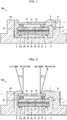
- Fig. 1 is a cross-sectional view illustrating an optical element package 100 in accordance with Embodiment 1 of the present invention.
- the optical element package 100 includes a package housing (housing) 1, an LCOS element (optical element) 2, a fixing resin (fixing member) 3, a bonding wire 4, and a sealing resin 5.
- the package housing 1 is a square-shaped housing constituted by a bottom plate 11 and a side plate 12.
- the LCOS element 2, the fixing resin 3, the bonding wire 4, and the sealing resin 5 are each contained in the package housing 1.
- the bottom plate 11 has a protruding section (fixing member) 11p formed thereon.
- the protruding section 11p is formed to be frame-like or in the form of at least three (3) columns (provided that the columns are not all aligned along a single straight line).
- the LCOS element 2 is a reflective optical element which (i) is contained in the package housing 1 and (ii) has a front surface 2f including an effective region, which front surface 2f is covered by a cover glass (transparent member) 21.
- the LCOS element 2 includes the cover glass 21, a substrate 22 made of silicon on which substrate a control circuit (not shown) is provided, a liquid crystal layer 23, a sealing member 24, a heater 25, and an adhesive resin 26.
- the optical element package 100 is configured such that a top 2t of the LCOS element 2 is positioned lower than a top 12t of the side plate 12.
- the substrate 22 is provided so as to be opposite the cover glass 21.
- the liquid crystal layer 23 is provided so as to be sandwiched between the cover glass 21 and the substrate 22. Note that an upper surface of the liquid crystal layer 23 corresponds to the effective region of the LCOS element 2.
- the sealing member 24 is made of resin and is provided so as to (i) be sandwiched between the cover glass 21 and the substrate 22 and (ii) surround the liquid crystal layer 23 from four sides.
- the sealing member 24, the cover glass 21, and the substrate 22 form a chamber in which the liquid crystal layer 23 is contained.
- the sealing member 24 can be made of, for example, (i) a photosensitive epoxy resin and/or (ii) a resin containing an acrylate compound. Note that a transparent conductive film and/or the like can be provided on an inner side of the cover glass 21, and an AR coating (anti-reflective coating) and/or the like can be provided on an outer side of the cover glass 21.
- the heater 25 serves to control this temperature.
- the heater 25 is provided on the protruding section 11p.
- the adhesive resin 26 serves to bond the substrate 22 to the heater 25. Specifically, the adhesive resin 26 bonds (i) a surface of the substrate 22, which surface faces away from the liquid crystal layer 23, to (ii) a surface of the heater 25, which surface faces away from the protruding section 11p.
- the fixing resin 3 serves to fix the heater 25 to the protruding section 11p.
- the fixing resin 3 can be applied to each of the columnar members constituting the protruding section 11p.
- the fixing resin 3 can be applied to a top surface of the protruding section 11p.
- the bonding wire 4 serves to electrically connect the package housing 1 to the substrate 22 of the LCOS element 2.
- the sealing resin 5 is filled into a gap between the LCOS element 2 and the package housing 1.
- the sealing resin 5 covers side surfaces 2s and a rear surface 2b of the LCOS element 2.
- the front surface 2f of the LCOS element 2 is covered by the cover glass 21, while the rear surface 2b and the side surfaces 2s of the LCOS element 2 are covered by the sealing resin 5.
- This makes it possible to hermetically seal the LCOS element 2 without providing a lid that could potentially block (i) light incident on the LCOS element 2 and (ii) light reflected by the LCOS element 2. It is therefore possible, with the optical element package 100, to increase the maximum angle of incidence and the maximum angle of output.
- the optical element package 100 makes possible a configuration having a reduced number of parts. This allows for a reduction in the amount of space which needs to be secured around the LCOS element 2 and therefore enables a reduction in size of the optical element package 100.
- the cover glass 21 is exposed to the atmosphere. This makes it easy to remove any foreign object which may be on the cover glass 21.
- sealing resin 5 surrounds the sealing member 24 of the LCOS element 2 from four sides. This makes it possible to prevent the sealing member 24 from being exposed and, therefore, makes it possible to enhance moisture resistance and waterproofness of the LCOS element 2.
- the sealing resin 5 covers the side surfaces 2s of the LCOS element 2 (and, in particular, surrounds the sealing member 24 from four sides).
- the sealing member 24 is made of a photosensitive epoxy resin and/or a resin containing an acrylate compound as described above, there is a risk that moisture will penetrate through the sealing member 24.
- a configuration in which the sealing 5 covers the side surfaces 2s (and, in particular, surrounds the sealing member 24 from four sides) is preferable because such a configuration makes it possible to prevent such penetration.
- the sealing resin 5 can be made of a light-blocking resin (for example, a black resin) or a light-transmitting resin.
- a configuration where the sealing resin 5 is made from a light-blocking resin makes it possible to suppress stray light.
- a configuration where the sealing resin 5 is made from a light-transmitting resin makes it possible for an inspector to visually inspect the interior of the package housing 1.
- the sealing resin 5 is preferably made from a resin having superior properties with regards to at least one of dampproofness, waterproofness, and chemical resistance.
- a resin having superior chemical resistance can also be said to have adequate resistance against corrosive gases. Examples of such a resin encompass a fluorosilicone gel, a fluorine gel, and a PPS (polyphenylene sulfide) resin.
- the sealing resin 5 is preferably in a gel form. Because the protruding section 11p and the fixing resin 3 serve to fix the LCOS element 2 to the package housing 1, the sealing resin 5 does not need to have a post-curing hardness sufficient for fixing the LCOS element 2 to the package housing 1. By not having a post-curing hardness sufficient for fixing the LCOS element 2 to the package housing 1, a resin in a gel form avoids creating stress strong enough to cause skewing of the LCOS element 2 during curing. This makes it possible for the LCOS element 2 to be contained in the optical element package 100 without being skewed. Examples of such a resin in a gel form encompass soft coating resins in a gel form, such as a silicone gel or a fluorosilicone gel.
- Embodiment 1 employs a configuration where a bottom surface of the heater 25 is fixed to the protruding section 1 1 p
- an alternative configuration where, for example, a member other than the heater 25 is fixed to the protruding section 11p.
- the cover glass 21 has a size larger than the sealing member 24, and (ii) a portion of the cover glass 21, which portion extends past the sealing member 24, is fixed to the protruding section 11p.
- the protruding section 11p can be configured to have a taller height.
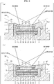
- Fig. 2 is a cross-sectional view illustrating an optical element package 200 in accordance with Embodiment 2 of the present invention.
- the optical element package 200 has a configuration which differs from that of the optical element package 100 with regards to the following points.
- the front surface 2f of the LCOS element 2 includes (i) an effective region (corresponding to the upper surface of a liquid crystal layer 23 and (ii) a non-effective region surrounding the effective region.
- an upper surface of a sealing member 24 corresponds to the non-effective region.
- the sealing resin 5 of Embodiment 2 further covers a region along an outer periphery of the non-effective region.
- the sealing resin 5 on the LCOS element 2 is formed to have inner walls whose respective angles of inclination ⁇ ta and ⁇ tb are each greater than 10° with respect to a direction of height of the optical element package 200. This is because, in the optical element package 200, light incident on the LCOS element 2 and/or light reflected by the LCOS element 2 will commonly have an angle of inclination of 10° or greater with respect to the direction of height of the optical element package 200.
- FIG. 3 (a) of Fig. 3 is a cross-sectional view illustrating an optical element package 300 in accordance with Embodiment 3 of the present invention.
- the optical element package 300 has a configuration which differs from that of the optical element package 100 with regards to the following points.
- the sealing resin 5 is filled, into the gap between the LCOS element 2 and the package housing 1, so as to rise to a position higher than (i) the top 12t of the side plate 12 and (ii) the top 2t of the LCOS element 2. Furthermore, the sealing resin 5 has angles of elevation ⁇ ga and ⁇ gb each having a maximum value that is less than 10°, the angles of elevation ⁇ ga and ⁇ gb each being obtained in a case where the sealing resin 5 is viewed from an outer edge of the effective region in a direction toward the outside of the effective region. Note here that the outer edge of the effective region refers to a position of a point obtained by projecting any point of a contour of the liquid crystal layer 23 onto a front surface of the cover glass 21.
- FIG. 3 (b) of Fig. 3 is a cross-sectional view illustrating an optical element package 301 in accordance with Embodiment 3 of the present invention.
- the optical element package 301 has a configuration which differs from that of the optical element package 100 with regards to the following points.
- the optical element package 301 is similar to the optical element package 100 in that the top 2t of the LCOS element 2 is positioned to be lower than the top 12t of the side plate 12.
- the sealing resin 5 is filled into the gap between the LCOS element 2 and the package housing 1 so as to be only in a region below imaginary straight lines sc and sd, each of which connects (i) the outer edge of the effective region to (ii) the top 12t of the side plate 12 along the shortest possible distance.
- the side plate 12 has angles of elevation ⁇ gc and ⁇ gd each having a maximum value that is less than 10°, the angles of elevation ⁇ gc and ⁇ gd each being obtained in a case where the side plate 12 is viewed from the outer edge of the effective region in a direction toward the outside of the effective region.
- the maximum angle of incidence and the maximum angle of output at the outer edge of the effective region are each obtained by subtracting the maximum value of a respective angle of elevation from 90°.
- the optical element packages 300 and 301 make it possible to set each of the maximum angle of incidence and the maximum angle of output at the outer edge of the effective region to be 80° or greater. That is, with the optical element packages 300 and 301, it is possible to set the maximum angle of incidence and the maximum angle of output of the optical element package to be 80° or greater.
- Fig. 4 is a cross-sectional view illustrating an optical element package 400 in accordance with Embodiment 4 of the present invention.
- the optical element package 400 has a configuration which differs from that of the optical element package 100 with regards to the following points.
- the optical element package 400 is configured such that (i) the top 2t of the LCOS element 2 has a height equivalent to that of the top 12t of the side plate 12 and (ii) a sealing resin 5 is provided only up to the same height as the top 2t of the LCOS element 2. In this configuration, there are no members above or beside the effective region which members would block incident light and output light. It is therefore possible, with the optical element package 400, to maximize the maximum angle of incidence and the maximum angle of output.
- Fig. 5 is a cross-sectional view illustrating an optical element package 500 in accordance with Embodiment 5 of the present invention.
- the optical element package 500 has a configuration which differs from that of the optical element package 100 with regards to the following points.
- the optical element package 500 is configured such that (i) the top 2t of the LCOS element 2 is positioned to be higher than the top 12t of the side plate 12 and (ii) the sealing resin 5 is provided only up to the same height as the top 2t of the LCOS element 2. In this configuration, there are no members above or beside the effective region which members would block incident light and output light. It is therefore possible, with the optical element package 500, to maximize the maximum angle of incidence and the maximum angle of output.
- An optical element package in accordance with an aspect of the present invention includes: a housing including a bottom plate and a side plate; and an optical element, being reflective, which (i) is contained in the housing and (ii) has a front surface including an effective region, the front surface being covered by a transparent member, a gap between the optical element and the housing being filled with a sealing resin which covers (i) side surfaces of the optical element and (ii) a rear surface of the optical element.
- the front surface of the optical element is covered by the transparent member, while the rear surface and the side surfaces of the optical element are covered by the sealing resin.
- This configuration therefore makes it possible to hermetically seal the optical element without providing a lid that could potentially block light incident on the optical element and light reflected by the optical element. It is therefore possible to increase the maximum angle of incidence and the maximum angle of output in comparison with the respective optical element packages of Patent Literatures 1 through 3.
- An optical element package in accordance with another aspect of the present invention is configured such that: the optical element is an LCOS element including: the transparent member; a substrate provided opposite the transparent member; a liquid crystal layer sandwiched between the transparent member and the substrate; and a sealing member, made of resin, which (i) is sandwiched between the transparent member and the substrate and (ii) surrounds the liquid crystal layer from four sides, and the sealing resin surrounds the sealing member from four sides.
- the optical element is an LCOS element including: the transparent member; a substrate provided opposite the transparent member; a liquid crystal layer sandwiched between the transparent member and the substrate; and a sealing member, made of resin, which (i) is sandwiched between the transparent member and the substrate and (ii) surrounds the liquid crystal layer from four sides, and the sealing resin surrounds the sealing member from four sides.
- the configuration makes it possible to prevent the sealing member of the LCOS element from being exposed and, therefore, makes it possible to enhance moisture resistance and waterproofness of the LCOS element.
- An optical element package in accordance with another aspect of the present invention is configured such that: the front surface of the optical element includes the effective region and a non-effective region surrounding the effective region; and the sealing resin further covers a region along an outer periphery of the non-effective region.
- the configuration makes it possible to more reliably prevent the sealing member of the LCOS element from being exposed, in comparison to a configuration where the sealing resin does not cover the front surface of the LCOS element at all. This makes it possible to further enhance moisture resistance and waterproofness of the LCOS element.
- An optical element package in accordance with another aspect of the present invention is configured such that: the sealing resin is filled into the gap between the optical element and the housing so as to rise to a position higher than (i) a top of the side plate and (ii) the front surface of the optical element; and the sealing resin has an angle of elevation whose maximum value is less than 10°, the angle of elevation being obtained in a case where the sealing resin is viewed from an outer edge of the effective region in a direction toward an outside of the effective region.
- the maximum angle of incidence and the maximum angle of output at the outer edge of the effective region are each obtained by subtracting the maximum value of the angle of elevation from 90°. With the configuration, it is possible to set each of the maximum angle of incidence and the maximum angle of output at the outer edge of the effective region to be 80° or greater. That is, it is possible to set the maximum angle of incidence and the maximum angle of output of the optical element package to be 80° or greater.
- An optical element package in accordance with another aspect of the present invention is configured such that: the front surface of the optical element is positioned to be lower than a top of the side plate; the sealing resin is filled into the gap between the optical element and the housing so as to be in a region below an imaginary straight line connecting (i) an outer edge of the effective region and (ii) the top of the side plate; and the side plate has an angle of elevation whose maximum value is less than 10°, the angle of elevation being obtained in a case where the side plate is viewed from the outer edge of the effective region in a direction toward an outside of the effective region.
- the maximum angle of incidence and the maximum angle of output at the outer edge of the effective region are each obtained by subtracting the maximum value of the angle of elevation from 90°. With the configuration, it is possible to set each of the maximum angle of incidence and the maximum angle of output at the outer edge of the effective region to be 80° or greater. That is, it is possible to set the maximum angle of incidence and the maximum angle of output of the optical element package to be 80° or greater.
- An optical element package in accordance with another aspect of the present invention is configured such that: the front surface of the optical element is positioned to be at a height equal to or greater than that of a top of the side plate; and the sealing resin is filled to a position whose height is equal to or less than that of a top of the optical element.
- An optical element package in accordance with another aspect of the present invention is configured to further include a fixing member for fixing the optical element to a portion of the housing, the sealing resin being in a gel form.
- the sealing resin does not need to have a post-curing hardness sufficient for fixing the optical element to the housing.
- a resin in a gel form avoids creating stress strong enough to cause skewing of the optical element during curing. This makes it possible for the optical element to be contained in the optical element package without being skewed.
Landscapes
- Physics & Mathematics (AREA)
- Nonlinear Science (AREA)
- Mathematical Physics (AREA)
- Chemical & Material Sciences (AREA)
- Crystallography & Structural Chemistry (AREA)
- General Physics & Mathematics (AREA)
- Optics & Photonics (AREA)
- Engineering & Computer Science (AREA)
- Microelectronics & Electronic Packaging (AREA)
- Liquid Crystal (AREA)
- Mechanical Light Control Or Optical Switches (AREA)
Abstract
Description
- The present invention relates to an optical element package in which an optical element, being reflective, is contained.
- A conventional optical element package is configured to include a housing and a lid thereof, which lid has an aperture through which light from outside the optical element package is incident upon an optical element in the housing. In order to hermetically seal the optical element, a light-transmitting glass member is provided so as to cover the aperture.
-
Patent Literature 1 discloses an optical switch module (optical element package) including a MEMS (Micro Electro Mechanical System) mirror array, as an optical element, in a housing. The optical element package includes a lid frame on an upper portion of the housing, and a glass member (sapphire in a plate-like form) is fixed to the lid frame via a fixing member. The lid frame has a rectangular aperture in its center, which aperture is covered by the glass member. -
Patent Literature 2 discloses an optical element package (optical element containment package) including a wavelength tunable interference filter, as an optical element, in a housing. The optical element package includes a lid on an upper portion of the housing, and a first window member is bonded to an outside of the lid, while a second window member is bonded to an inside of the lid. The lid has a circular aperture in its center, which aperture is covered by the first window member and the second window member. -
Patent Literature 3 discloses an optical element package including a wavelength tunable interference filter, as an optical element, in a housing. The optical element package includes a lid on an upper portion of the housing, and a glass member is fixed to the lid via a fixing member. The lid has a circular aperture in its center, which aperture is covered by the glass member. -
- [Patent Literature 1]
Japanese Patent Application Publication, Tokukai, No. 2011-8105 (Publication date: January 13, 2011 - [Patent Literature 2]
Japanese Patent Application Publication, Tokukai, No. 2014-82348 (Publication date: May 8, 2014 - [Patent Literature 3]
Japanese Patent Application Publication, Tokukai, No. 2015-31903 (Publication date: February 16, 2015 - Unfortunately, the conventional optical element package has a problem that the lid blocks (i) incident light having a large angle of incidence with respect to a direction normal to a front surface of the optical element and (ii) light outputted by the optical element (for example, reflected light) which light has a large angle of output with respect to the direction normal to the front surface of the optical element. In other words, the angle of incidence and the angle of output each have a maximum value (hereinafter respectively referred to as a "maximum angle of incidence" and a "maximum angle of output").
- The maximum angle of incidence is defined by (i) a size of the aperture and (ii) a distance between the front surface of the optical element and a top of the aperture. In order to increase the maximum angle of incidence, it is preferable that (i) the aperture is sufficiently large with respect to a size of an effective region of the optical element and (ii) the distance between the front surface of the optical element and the top of the aperture is as small as possible. The same applies to the maximum angle of output.
- With the conventional optical element package, however, increasing the size of the aperture directly causes an increase in a size of the optical element package. This makes it impractical to set the size of the aperture to be larger than the effective region of the optical element.
- Furthermore, the distance between (i) the front surface of the optical element and (ii) the top of the aperture formed in the lid must be at least equivalent to a thickness of the lid. In order to secure strength of the housing, there is a minimum possible value to which the thickness of the lid can be set. As such, it is impractical to set the distance to be exceedingly short. Note that, as illustrated in
Fig. 3 ofPatent Literature 1, the distance is greater than the thickness of the lid because (i) the window member is provided between the optical element and the lid and (ii) the optical element and the window member are separated from each other. - Thus, as explained above, it is difficult to (i) set the size of the aperture to be larger than the effective region of the optical element and (ii) set the distance between the front surface of the optical element and the top of the aperture to be small. This makes it difficult, in the conventional optical element package, to increase the maximum angle of incidence and the maximum angle of output.
- The present invention has been made in view of the above problems. An object of the present invention lies in increasing a maximum angle of incidence and a maximum angle of output, of an optical element package, with respect to an optical element contained therein, the optical element being reflective.
- In order to solve the above problem, an optical element package in accordance with an aspect of the present invention includes: a housing including a bottom plate and a side plate; and an optical element, being reflective, which (i) is contained in the housing and (ii) has a front surface including an effective region, the front surface being covered by a transparent member, a gap between the optical element and the housing being filled with a sealing resin which covers (i) side surfaces of the optical element and (ii) a rear surface of the optical element.
- An aspect of the present invention makes it possible to increase an angle of incidence and an angle of output in an optical element package which includes an optical element, being reflective, in its housing.
-
-
Fig. 1 is a cross-sectional view illustrating an optical element package in accordance withEmbodiment 1 of the present invention. -
Fig. 2 is a cross-sectional view illustrating an optical element package in accordance withEmbodiment 2 of the present invention. - (a) and (b) of
Fig. 3 are each a cross-sectional view illustrating an optical element package in accordance withEmbodiment 3 of the present invention. -
Fig. 4 is a cross-sectional view illustrating an optical element package in accordance withEmbodiment 4 of the present invention. -
Fig. 5 is a cross-sectional view illustrating an optical element package in accordance withEmbodiment 5 of the present invention. - The following description will discuss embodiments of the present invention with reference to
Figs. 1 through 5 . Note that, for convenience, in each of the following embodiments, members having functions identical to those of the respective members described in another embodiment are given respective identical reference numerals, and a duplicate description of those members is omitted. -
Fig. 1 is a cross-sectional view illustrating anoptical element package 100 in accordance withEmbodiment 1 of the present invention. Theoptical element package 100 includes a package housing (housing) 1, an LCOS element (optical element) 2, a fixing resin (fixing member) 3, abonding wire 4, and asealing resin 5. - The
package housing 1 is a square-shaped housing constituted by abottom plate 11 and aside plate 12. TheLCOS element 2, thefixing resin 3, thebonding wire 4, and the sealingresin 5 are each contained in thepackage housing 1. Thebottom plate 11 has a protruding section (fixing member) 11p formed thereon. Theprotruding section 11p is formed to be frame-like or in the form of at least three (3) columns (provided that the columns are not all aligned along a single straight line). - The
LCOS element 2 is a reflective optical element which (i) is contained in thepackage housing 1 and (ii) has afront surface 2f including an effective region, whichfront surface 2f is covered by a cover glass (transparent member) 21. TheLCOS element 2 includes thecover glass 21, asubstrate 22 made of silicon on which substrate a control circuit (not shown) is provided, aliquid crystal layer 23, asealing member 24, aheater 25, and anadhesive resin 26. Theoptical element package 100 is configured such that a top 2t of theLCOS element 2 is positioned lower than a top 12t of theside plate 12. - The
substrate 22 is provided so as to be opposite thecover glass 21. Theliquid crystal layer 23 is provided so as to be sandwiched between thecover glass 21 and thesubstrate 22. Note that an upper surface of theliquid crystal layer 23 corresponds to the effective region of theLCOS element 2. The sealingmember 24 is made of resin and is provided so as to (i) be sandwiched between thecover glass 21 and thesubstrate 22 and (ii) surround theliquid crystal layer 23 from four sides. The sealingmember 24, thecover glass 21, and thesubstrate 22 form a chamber in which theliquid crystal layer 23 is contained. The sealingmember 24 can be made of, for example, (i) a photosensitive epoxy resin and/or (ii) a resin containing an acrylate compound. Note that a transparent conductive film and/or the like can be provided on an inner side of thecover glass 21, and an AR coating (anti-reflective coating) and/or the like can be provided on an outer side of thecover glass 21. - It is necessary to carefully manage the temperature of the
LCOS element 2, and theheater 25 serves to control this temperature. Theheater 25 is provided on the protrudingsection 11p. Theadhesive resin 26 serves to bond thesubstrate 22 to theheater 25. Specifically, theadhesive resin 26 bonds (i) a surface of thesubstrate 22, which surface faces away from theliquid crystal layer 23, to (ii) a surface of theheater 25, which surface faces away from the protrudingsection 11p. - The fixing
resin 3 serves to fix theheater 25 to the protrudingsection 11p. In a case where the protrudingsection 11p is configured to be constituted by three (3) or more columnar members, the fixingresin 3 can be applied to each of the columnar members constituting the protrudingsection 11p. In a case where the protrudingsection 11p is configured to be frame-like, the fixingresin 3 can be applied to a top surface of the protrudingsection 11p. Thebonding wire 4 serves to electrically connect thepackage housing 1 to thesubstrate 22 of theLCOS element 2. - The sealing
resin 5 is filled into a gap between theLCOS element 2 and thepackage housing 1. The sealingresin 5 coversside surfaces 2s and arear surface 2b of theLCOS element 2. As such, thefront surface 2f of theLCOS element 2 is covered by thecover glass 21, while therear surface 2b and the side surfaces 2s of theLCOS element 2 are covered by the sealingresin 5. This makes it possible to hermetically seal theLCOS element 2 without providing a lid that could potentially block (i) light incident on theLCOS element 2 and (ii) light reflected by theLCOS element 2. It is therefore possible, with theoptical element package 100, to increase the maximum angle of incidence and the maximum angle of output. Note that since a lid is unnecessary theoptical element package 100 makes possible a configuration having a reduced number of parts. This allows for a reduction in the amount of space which needs to be secured around theLCOS element 2 and therefore enables a reduction in size of theoptical element package 100. - With the configuration of the
optical element package 100, thecover glass 21 is exposed to the atmosphere. This makes it easy to remove any foreign object which may be on thecover glass 21. - Note also that the sealing
resin 5 surrounds the sealingmember 24 of theLCOS element 2 from four sides. This makes it possible to prevent the sealingmember 24 from being exposed and, therefore, makes it possible to enhance moisture resistance and waterproofness of theLCOS element 2. - The following description will discuss, in further detail, an advantage of a configuration in which the sealing
resin 5 covers the side surfaces 2s of the LCOS element 2 (and, in particular, surrounds the sealingmember 24 from four sides). In a case where the sealingmember 24 is made of a photosensitive epoxy resin and/or a resin containing an acrylate compound as described above, there is a risk that moisture will penetrate through the sealingmember 24. A configuration in which the sealing 5 covers the side surfaces 2s (and, in particular, surrounds the sealingmember 24 from four sides) is preferable because such a configuration makes it possible to prevent such penetration. - The sealing
resin 5 can be made of a light-blocking resin (for example, a black resin) or a light-transmitting resin. A configuration where the sealingresin 5 is made from a light-blocking resin makes it possible to suppress stray light. A configuration where the sealingresin 5 is made from a light-transmitting resin makes it possible for an inspector to visually inspect the interior of thepackage housing 1. - The sealing
resin 5 is preferably made from a resin having superior properties with regards to at least one of dampproofness, waterproofness, and chemical resistance. A resin having superior chemical resistance can also be said to have adequate resistance against corrosive gases. Examples of such a resin encompass a fluorosilicone gel, a fluorine gel, and a PPS (polyphenylene sulfide) resin. - The sealing
resin 5 is preferably in a gel form. Because the protrudingsection 11p and the fixingresin 3 serve to fix theLCOS element 2 to thepackage housing 1, the sealingresin 5 does not need to have a post-curing hardness sufficient for fixing theLCOS element 2 to thepackage housing 1. By not having a post-curing hardness sufficient for fixing theLCOS element 2 to thepackage housing 1, a resin in a gel form avoids creating stress strong enough to cause skewing of theLCOS element 2 during curing. This makes it possible for theLCOS element 2 to be contained in theoptical element package 100 without being skewed. Examples of such a resin in a gel form encompass soft coating resins in a gel form, such as a silicone gel or a fluorosilicone gel. - Note that although
Embodiment 1 employs a configuration where a bottom surface of theheater 25 is fixed to the protrudingsection 1 1 p, it is also possible to employ an alternative configuration where, for example, a member other than theheater 25 is fixed to the protrudingsection 11p. For example, it is possible to employ a configuration where (i) thecover glass 21 has a size larger than the sealingmember 24, and (ii) a portion of thecover glass 21, which portion extends past the sealingmember 24, is fixed to the protrudingsection 11p. In such a case, the protrudingsection 11p can be configured to have a taller height. -
Fig. 2 is a cross-sectional view illustrating anoptical element package 200 in accordance withEmbodiment 2 of the present invention. Theoptical element package 200 has a configuration which differs from that of theoptical element package 100 with regards to the following points. - In
Embodiment 2, thefront surface 2f of theLCOS element 2 includes (i) an effective region (corresponding to the upper surface of aliquid crystal layer 23 and (ii) a non-effective region surrounding the effective region. Note that an upper surface of a sealingmember 24 corresponds to the non-effective region. The sealingresin 5 ofEmbodiment 2 further covers a region along an outer periphery of the non-effective region. - This makes it possible to more reliably prevent the sealing
member 24 of theLCOS element 2 from being exposed, in comparison to a configuration where the sealingresin 5 does not cover thefront surface 2f of theLCOS element 2 at all. This makes it possible to further enhance moisture resistance and waterproofness of theLCOS element 2. - Note here that it is preferable that the sealing
resin 5 on theLCOS element 2 is formed to have inner walls whose respective angles of inclination θ ta and θ tb are each greater than 10° with respect to a direction of height of theoptical element package 200. This is because, in theoptical element package 200, light incident on theLCOS element 2 and/or light reflected by theLCOS element 2 will commonly have an angle of inclination of 10° or greater with respect to the direction of height of theoptical element package 200. - (a) of
Fig. 3 is a cross-sectional view illustrating anoptical element package 300 in accordance withEmbodiment 3 of the present invention. Theoptical element package 300 has a configuration which differs from that of theoptical element package 100 with regards to the following points. - In
Embodiment 3, the sealingresin 5 is filled, into the gap between theLCOS element 2 and thepackage housing 1, so as to rise to a position higher than (i) the top 12t of theside plate 12 and (ii) the top 2t of theLCOS element 2. Furthermore, the sealingresin 5 has angles of elevation θ ga and θ gb each having a maximum value that is less than 10°, the angles of elevation θ ga and θ gb each being obtained in a case where the sealingresin 5 is viewed from an outer edge of the effective region in a direction toward the outside of the effective region. Note here that the outer edge of the effective region refers to a position of a point obtained by projecting any point of a contour of theliquid crystal layer 23 onto a front surface of thecover glass 21. - (b) of
Fig. 3 is a cross-sectional view illustrating anoptical element package 301 in accordance withEmbodiment 3 of the present invention. Theoptical element package 301 has a configuration which differs from that of theoptical element package 100 with regards to the following points. - The
optical element package 301 is similar to theoptical element package 100 in that the top 2t of theLCOS element 2 is positioned to be lower than the top 12t of theside plate 12. In theoptical element package 301, however, the sealingresin 5 is filled into the gap between theLCOS element 2 and thepackage housing 1 so as to be only in a region below imaginary straight lines sc and sd, each of which connects (i) the outer edge of the effective region to (ii) the top 12t of theside plate 12 along the shortest possible distance. Furthermore, theside plate 12 has angles of elevation θ gc and θ gd each having a maximum value that is less than 10°, the angles of elevation θ gc and θ gd each being obtained in a case where theside plate 12 is viewed from the outer edge of the effective region in a direction toward the outside of the effective region. - The maximum angle of incidence and the maximum angle of output at the outer edge of the effective region are each obtained by subtracting the maximum value of a respective angle of elevation from 90°. The optical element packages 300 and 301 make it possible to set each of the maximum angle of incidence and the maximum angle of output at the outer edge of the effective region to be 80° or greater. That is, with the optical element packages 300 and 301, it is possible to set the maximum angle of incidence and the maximum angle of output of the optical element package to be 80° or greater.
- This also makes it possible to suppress an effect, of reflection from an optical part outside the
LCOS element 2, on light incident on and output by theLCOS element 2. As such, it is possible to better isolate a signal in each port and suppress crosstalk. -
Fig. 4 is a cross-sectional view illustrating anoptical element package 400 in accordance withEmbodiment 4 of the present invention. Theoptical element package 400 has a configuration which differs from that of theoptical element package 100 with regards to the following points. - The
optical element package 400 is configured such that (i) the top 2t of theLCOS element 2 has a height equivalent to that of the top 12t of theside plate 12 and (ii) a sealingresin 5 is provided only up to the same height as the top 2t of theLCOS element 2. In this configuration, there are no members above or beside the effective region which members would block incident light and output light. It is therefore possible, with theoptical element package 400, to maximize the maximum angle of incidence and the maximum angle of output. -
Fig. 5 is a cross-sectional view illustrating anoptical element package 500 in accordance withEmbodiment 5 of the present invention. Theoptical element package 500 has a configuration which differs from that of theoptical element package 100 with regards to the following points. - The
optical element package 500 is configured such that (i) the top 2t of theLCOS element 2 is positioned to be higher than the top 12t of theside plate 12 and (ii) the sealingresin 5 is provided only up to the same height as the top 2t of theLCOS element 2. In this configuration, there are no members above or beside the effective region which members would block incident light and output light. It is therefore possible, with theoptical element package 500, to maximize the maximum angle of incidence and the maximum angle of output. - An optical element package in accordance with an aspect of the present invention includes: a housing including a bottom plate and a side plate; and an optical element, being reflective, which (i) is contained in the housing and (ii) has a front surface including an effective region, the front surface being covered by a transparent member, a gap between the optical element and the housing being filled with a sealing resin which covers (i) side surfaces of the optical element and (ii) a rear surface of the optical element.
- With the configuration, the front surface of the optical element is covered by the transparent member, while the rear surface and the side surfaces of the optical element are covered by the sealing resin. This configuration therefore makes it possible to hermetically seal the optical element without providing a lid that could potentially block light incident on the optical element and light reflected by the optical element. It is therefore possible to increase the maximum angle of incidence and the maximum angle of output in comparison with the respective optical element packages of
Patent Literatures 1 through 3. - An optical element package in accordance with another aspect of the present invention is configured such that: the optical element is an LCOS element including: the transparent member; a substrate provided opposite the transparent member; a liquid crystal layer sandwiched between the transparent member and the substrate; and a sealing member, made of resin, which (i) is sandwiched between the transparent member and the substrate and (ii) surrounds the liquid crystal layer from four sides, and the sealing resin surrounds the sealing member from four sides.
- The configuration makes it possible to prevent the sealing member of the LCOS element from being exposed and, therefore, makes it possible to enhance moisture resistance and waterproofness of the LCOS element.
- An optical element package in accordance with another aspect of the present invention is configured such that: the front surface of the optical element includes the effective region and a non-effective region surrounding the effective region; and the sealing resin further covers a region along an outer periphery of the non-effective region.
- The configuration makes it possible to more reliably prevent the sealing member of the LCOS element from being exposed, in comparison to a configuration where the sealing resin does not cover the front surface of the LCOS element at all. This makes it possible to further enhance moisture resistance and waterproofness of the LCOS element.
- An optical element package in accordance with another aspect of the present invention is configured such that: the sealing resin is filled into the gap between the optical element and the housing so as to rise to a position higher than (i) a top of the side plate and (ii) the front surface of the optical element; and the sealing resin has an angle of elevation whose maximum value is less than 10°, the angle of elevation being obtained in a case where the sealing resin is viewed from an outer edge of the effective region in a direction toward an outside of the effective region.
- The maximum angle of incidence and the maximum angle of output at the outer edge of the effective region are each obtained by subtracting the maximum value of the angle of elevation from 90°. With the configuration, it is possible to set each of the maximum angle of incidence and the maximum angle of output at the outer edge of the effective region to be 80° or greater. That is, it is possible to set the maximum angle of incidence and the maximum angle of output of the optical element package to be 80° or greater.
- An optical element package in accordance with another aspect of the present invention is configured such that: the front surface of the optical element is positioned to be lower than a top of the side plate; the sealing resin is filled into the gap between the optical element and the housing so as to be in a region below an imaginary straight line connecting (i) an outer edge of the effective region and (ii) the top of the side plate; and the side plate has an angle of elevation whose maximum value is less than 10°, the angle of elevation being obtained in a case where the side plate is viewed from the outer edge of the effective region in a direction toward an outside of the effective region.
- The maximum angle of incidence and the maximum angle of output at the outer edge of the effective region are each obtained by subtracting the maximum value of the angle of elevation from 90°. With the configuration, it is possible to set each of the maximum angle of incidence and the maximum angle of output at the outer edge of the effective region to be 80° or greater. That is, it is possible to set the maximum angle of incidence and the maximum angle of output of the optical element package to be 80° or greater.
- An optical element package in accordance with another aspect of the present invention is configured such that: the front surface of the optical element is positioned to be at a height equal to or greater than that of a top of the side plate; and the sealing resin is filled to a position whose height is equal to or less than that of a top of the optical element.
- In the configuration, there are no members above or beside the effective region which members would block incident light and output light. It is therefore possible to maximize the maximum angle of incidence and the maximum angle of output of the optical element package.
- An optical element package in accordance with another aspect of the present invention is configured to further include a fixing member for fixing the optical element to a portion of the housing, the sealing resin being in a gel form.
- With the configuration, because the fixing member serves to fix the optical element to the housing, the sealing resin does not need to have a post-curing hardness sufficient for fixing the optical element to the housing. By not having a post-curing hardness sufficient for fixing the optical element to the housing, a resin in a gel form avoids creating stress strong enough to cause skewing of the optical element during curing. This makes it possible for the optical element to be contained in the optical element package without being skewed.
- The present invention is not limited to the embodiments, but can be altered by a skilled person in the art within the scope of the claims. An embodiment derived from a proper combination of technical means each disclosed in a different embodiment is also encompassed in the technical scope of the present invention.
-
- 1 Package housing (housing)
- 2 LCOS element (optical element)
- 2b Rear surface of LCOS element
- 2f Front surface of LCOS element
- 2s Side surface of LCOS element
- 2t Top of LCOS element
- 3 Fixing resin (fixing member)
- 4 Bonding wire
- 5 Sealing resin
- 11 Bottom plate
- 11p Protruding section (fixing member)
- 12 Side plate
- 12t Top of side plate
- 21 Cover glass (transparent member)
- 22 Substrate
- 23 Liquid crystal layer
- 24 Sealing member
- 25 Heater
- 26 Adhesive resin
- 100, 200, 300, 301, 400, 500 Optical element package
- θ ga, θ gb, θ gc, θ gd Angle of elevation
Claims (7)
- An optical element package comprising:a housing including a bottom plate and a side plate; andan optical element, being reflective, which (i) is contained in the housing and (ii) has a front surface including an effective region, the front surface being covered by a transparent member,a gap between the optical element and the housing being filled with a sealing resin which covers (i) side surfaces of the optical element and (ii) a rear surface of the optical element.
- The optical element package as set forth in claim 1, wherein:the optical element is an LCOS element including:the transparent member;a substrate provided opposite the transparent member;a liquid crystal layer sandwiched between the transparent member and the substrate; anda sealing member, made of resin, which (i) is sandwiched between the transparent member and the substrate and (ii) surrounds the liquid crystal layer from four sides, andthe sealing resin surrounds the sealing member from four sides.
- The optical element package as set forth in claim 2, wherein:the front surface of the optical element includes the effective region and a non-effective region surrounding the effective region; andthe sealing resin further covers a region along an outer periphery of the non-effective region.
- The optical element package as set forth in any one of claims 1 through 3, wherein:
the sealing resin is filled into the gap between the optical element and the housing so as to rise to a position higher than (i) a top of the side plate and (ii) the front surface of the optical element; and
the sealing resin has an angle of elevation whose maximum value is less than 10°, the angle of elevation being obtained in a case where the sealing resin is viewed from an outer edge of the effective region in a direction toward an outside of the effective region. - The optical element package as set forth in any one of claims 1 through 3, wherein:the front surface of the optical element is positioned to be lower than a top of the side plate;the sealing resin is filled into the gap between the optical element and the housing so as to be in a region below an imaginary straight line connecting (i) an outer edge of the effective region and (ii) the top of the side plate; andthe side plate has an angle of elevation whose maximum value is less than 10°, the angle of elevation being obtained in a case where the side plate is viewed from the outer edge of the effective region in a direction toward an outside of the effective region.
- The optical element package as set forth in any one of claims 1 through 3, wherein:the front surface of the optical element is positioned to be at a height equal to or greater than that of a top of the side plate; andthe sealing resin is filled to a position whose height is equal to or less than that of a top of the optical element.
- The optical element package as set forth in any one of claims 1 through 6, further comprising a fixing member for fixing the optical element to a portion of the housing,
the sealing resin being in a gel form.
Applications Claiming Priority (2)
| Application Number | Priority Date | Filing Date | Title |
|---|---|---|---|
| JP2015252131A JP6529431B2 (en) | 2015-12-24 | 2015-12-24 | Optical element package |
| PCT/JP2016/077654 WO2017110176A1 (en) | 2015-12-24 | 2016-09-20 | Optical element package |
Publications (2)
| Publication Number | Publication Date |
|---|---|
| EP3211474A1 true EP3211474A1 (en) | 2017-08-30 |
| EP3211474A4 EP3211474A4 (en) | 2018-08-01 |
Family
ID=59089945
Family Applications (1)
| Application Number | Title | Priority Date | Filing Date |
|---|---|---|---|
| EP16837996.4A Withdrawn EP3211474A4 (en) | 2015-12-24 | 2016-09-20 | Optical element package |
Country Status (5)
| Country | Link |
|---|---|
| US (1) | US10386665B2 (en) |
| EP (1) | EP3211474A4 (en) |
| JP (1) | JP6529431B2 (en) |
| CN (1) | CN107250898A (en) |
| WO (1) | WO2017110176A1 (en) |
Families Citing this family (6)
| Publication number | Priority date | Publication date | Assignee | Title |
|---|---|---|---|---|
| US10488721B2 (en) | 2017-09-18 | 2019-11-26 | Omnivision Technologies, Inc. | Liquid crystal on silicon packaging |
| CN113359351B (en) * | 2021-06-17 | 2022-07-12 | 武汉华星光电技术有限公司 | Backlight module and display device |
| US11520442B1 (en) * | 2021-08-12 | 2022-12-06 | Rockwell Automation Technologies, Inc. | Industrial automation display device with touchscreen |
| CN115421333B (en) * | 2022-09-21 | 2024-07-26 | 豪威半导体(上海)有限责任公司 | LCOS packaging structure and packaging method |
| KR20250173488A (en) | 2023-04-21 | 2025-12-10 | 하마마츠 포토닉스 가부시키가이샤 | Phase modulation module |
| KR20250170057A (en) | 2023-04-21 | 2025-12-04 | 하마마츠 포토닉스 가부시키가이샤 | Phase modulation module |
Family Cites Families (19)
| Publication number | Priority date | Publication date | Assignee | Title |
|---|---|---|---|---|
| JPH10123983A (en) * | 1996-08-30 | 1998-05-15 | Sony Corp | Liquid crystal display |
| JPH11327448A (en) * | 1998-05-12 | 1999-11-26 | Idemitsu Kosan Co Ltd | Display device |
| DE60014829D1 (en) * | 1999-05-21 | 2004-11-18 | Citizen Watch Co Ltd | Liquid crystal display panel |
| JP2002296568A (en) | 2001-03-29 | 2002-10-09 | Victor Co Of Japan Ltd | Reflection type liquid crystal display element and manufacturing method therefor |
| JP3891843B2 (en) * | 2002-01-08 | 2007-03-14 | 株式会社日立製作所 | Liquid crystal display |
| JP2005215335A (en) * | 2004-01-29 | 2005-08-11 | Victor Co Of Japan Ltd | Liquid crystal display |
| US7399084B2 (en) | 2004-04-09 | 2008-07-15 | Matsushita Electric Industrial Co., Ltd. | Laser image display apparatus |
| JP4432937B2 (en) * | 2006-06-06 | 2010-03-17 | セイコーエプソン株式会社 | Electro-optical device and electronic apparatus including the same |
| JP2009163132A (en) * | 2008-01-09 | 2009-07-23 | Seiko Instruments Inc | Liquid crystal display device manufacturing method, liquid crystal display device, and electronic apparatus |
| JP5268761B2 (en) * | 2008-05-26 | 2013-08-21 | 三菱電機株式会社 | Display device and manufacturing method thereof |
| JP5161160B2 (en) | 2009-06-26 | 2013-03-13 | 日本電信電話株式会社 | Optical switch module |
| US9069201B2 (en) * | 2010-03-19 | 2015-06-30 | Balboa Wter Group, Inc. | Waterproof user interface display panels |
| TWI440934B (en) * | 2010-04-27 | 2014-06-11 | Lg Display Co Ltd | Display device |
| US20130308075A1 (en) * | 2010-09-27 | 2013-11-21 | Sharp Kabushiki Kaisha | Liquid crystal module and electronic apparatus |
| KR20120071751A (en) * | 2010-12-23 | 2012-07-03 | 엘지디스플레이 주식회사 | Display device |
| JP2012220525A (en) * | 2011-04-04 | 2012-11-12 | Seiko Epson Corp | Liquid crystal device and projector |
| JP2014082348A (en) | 2012-10-17 | 2014-05-08 | Seiko Epson Corp | Package for storing optical element, optical filter device, optical module, and electronic apparatus |
| DE102013203531B3 (en) * | 2013-03-01 | 2014-05-22 | Magna Mirrors Holding Gmbh | Rearview mirror assembly for motor vehicles |
| JP2015031903A (en) | 2013-08-06 | 2015-02-16 | セイコーエプソン株式会社 | Optical device, optical module, electronic apparatus, and optical housing |
-
2015
- 2015-12-24 JP JP2015252131A patent/JP6529431B2/en not_active Expired - Fee Related
-
2016
- 2016-09-20 CN CN201680002380.XA patent/CN107250898A/en active Pending
- 2016-09-20 US US15/508,246 patent/US10386665B2/en not_active Expired - Fee Related
- 2016-09-20 EP EP16837996.4A patent/EP3211474A4/en not_active Withdrawn
- 2016-09-20 WO PCT/JP2016/077654 patent/WO2017110176A1/en not_active Ceased
Also Published As
| Publication number | Publication date |
|---|---|
| EP3211474A4 (en) | 2018-08-01 |
| US10386665B2 (en) | 2019-08-20 |
| US20180113351A1 (en) | 2018-04-26 |
| JP6529431B2 (en) | 2019-06-12 |
| WO2017110176A1 (en) | 2017-06-29 |
| CN107250898A (en) | 2017-10-13 |
| JP2017116735A (en) | 2017-06-29 |
Similar Documents
| Publication | Publication Date | Title |
|---|---|---|
| US10386665B2 (en) | Optical element package | |
| EP2084896B1 (en) | Control of stray light in camera systems employing an optics stack and associated methods | |
| CN109283736B (en) | Display screen and electronic equipment | |
| JP6390117B2 (en) | Optical module and electronic device | |
| EP2747411A1 (en) | Imaging element module and method for manufacturing same | |
| KR100575094B1 (en) | Module for optical device, and manufacturing method therefor | |
| CN117872555A (en) | Lens unit and camera module | |
| KR100862486B1 (en) | Camera module package | |
| US11604093B2 (en) | Spectrometer device and method for producing a spectrometer device | |
| CN103941315A (en) | Optical device storage package, optical module, filter device, and electronic apparatus | |
| US10007137B2 (en) | Optical device package | |
| US20170227811A1 (en) | Optical device package, optical switch, and method for manufacturing optical device package | |
| JP2008193441A (en) | Optical device and manufacturing method thereof | |
| JPS61112480A (en) | Solid-state image pickup structure | |
| JP2010192866A (en) | Optical device, solid-state imaging device, and optical device manufacturing method | |
| JP5996328B2 (en) | Semiconductor device | |
| KR20260036361A (en) | Camera module including an encapsulated meta-optical system | |
| CN106019575A (en) | Method for manufacturing electro-optical device, electro-optical device, and electronic apparatus | |
| US20170276704A1 (en) | Optical device package and optical switch | |
| US20170278886A1 (en) | Optical device and production method for optical device | |
| CN112384469A (en) | Method for manufacturing micromechanical device with tilted optical window and micromechanical device with tilted optical window | |
| JP6306317B2 (en) | Reflective liquid crystal display | |
| WO2011117947A1 (en) | Optical semiconductor device |
Legal Events
| Date | Code | Title | Description |
|---|---|---|---|
| STAA | Information on the status of an ep patent application or granted ep patent |
Free format text: STATUS: UNKNOWN |
|
| STAA | Information on the status of an ep patent application or granted ep patent |
Free format text: STATUS: THE INTERNATIONAL PUBLICATION HAS BEEN MADE |
|
| PUAI | Public reference made under article 153(3) epc to a published international application that has entered the european phase |
Free format text: ORIGINAL CODE: 0009012 |
|
| STAA | Information on the status of an ep patent application or granted ep patent |
Free format text: STATUS: REQUEST FOR EXAMINATION WAS MADE |
|
| 17P | Request for examination filed |
Effective date: 20170228 |
|
| AK | Designated contracting states |
Kind code of ref document: A1 Designated state(s): AL AT BE BG CH CY CZ DE DK EE ES FI FR GB GR HR HU IE IS IT LI LT LU LV MC MK MT NL NO PL PT RO RS SE SI SK SM TR |
|
| AX | Request for extension of the european patent |
Extension state: BA ME |
|
| A4 | Supplementary search report drawn up and despatched |
Effective date: 20180704 |
|
| RIC1 | Information provided on ipc code assigned before grant |
Ipc: G02F 1/1333 20060101AFI20180628BHEP Ipc: G02F 1/1362 20060101ALN20180628BHEP |
|
| DAV | Request for validation of the european patent (deleted) | ||
| DAX | Request for extension of the european patent (deleted) | ||
| STAA | Information on the status of an ep patent application or granted ep patent |
Free format text: STATUS: EXAMINATION IS IN PROGRESS |
|
| STAA | Information on the status of an ep patent application or granted ep patent |
Free format text: STATUS: THE APPLICATION HAS BEEN WITHDRAWN |
|
| 17Q | First examination report despatched |
Effective date: 20200320 |
|
| 18W | Application withdrawn |
Effective date: 20200414 |