EP3211409A1 - Integrated capacitive humidity sensor - Google Patents
Integrated capacitive humidity sensor Download PDFInfo
- Publication number
- EP3211409A1 EP3211409A1 EP17154932.2A EP17154932A EP3211409A1 EP 3211409 A1 EP3211409 A1 EP 3211409A1 EP 17154932 A EP17154932 A EP 17154932A EP 3211409 A1 EP3211409 A1 EP 3211409A1
- Authority
- EP
- European Patent Office
- Prior art keywords
- layer
- electrically conductive
- polymer layer
- conductive metal
- polymer
- Prior art date
- Legal status (The legal status is an assumption and is not a legal conclusion. Google has not performed a legal analysis and makes no representation as to the accuracy of the status listed.)
- Granted
Links
Images






Classifications
-
- G—PHYSICS
- G01—MEASURING; TESTING
- G01N—INVESTIGATING OR ANALYSING MATERIALS BY DETERMINING THEIR CHEMICAL OR PHYSICAL PROPERTIES
- G01N27/00—Investigating or analysing materials by the use of electric, electrochemical, or magnetic means
- G01N27/02—Investigating or analysing materials by the use of electric, electrochemical, or magnetic means by investigating impedance
- G01N27/22—Investigating or analysing materials by the use of electric, electrochemical, or magnetic means by investigating impedance by investigating capacitance
- G01N27/223—Investigating or analysing materials by the use of electric, electrochemical, or magnetic means by investigating impedance by investigating capacitance for determining moisture content, e.g. humidity
-
- B—PERFORMING OPERATIONS; TRANSPORTING
- B81—MICROSTRUCTURAL TECHNOLOGY
- B81B—MICROSTRUCTURAL DEVICES OR SYSTEMS, e.g. MICROMECHANICAL DEVICES
- B81B7/00—Microstructural systems ; Auxiliary parts of microstructural devices or systems
- B81B7/008—MEMS characterised by an electronic circuit specially adapted for controlling or driving the same
-
- G—PHYSICS
- G01—MEASURING; TESTING
- G01N—INVESTIGATING OR ANALYSING MATERIALS BY DETERMINING THEIR CHEMICAL OR PHYSICAL PROPERTIES
- G01N27/00—Investigating or analysing materials by the use of electric, electrochemical, or magnetic means
- G01N27/02—Investigating or analysing materials by the use of electric, electrochemical, or magnetic means by investigating impedance
- G01N27/22—Investigating or analysing materials by the use of electric, electrochemical, or magnetic means by investigating impedance by investigating capacitance
- G01N27/223—Investigating or analysing materials by the use of electric, electrochemical, or magnetic means by investigating impedance by investigating capacitance for determining moisture content, e.g. humidity
- G01N27/225—Investigating or analysing materials by the use of electric, electrochemical, or magnetic means by investigating impedance by investigating capacitance for determining moisture content, e.g. humidity by using hygroscopic materials
-
- B—PERFORMING OPERATIONS; TRANSPORTING
- B81—MICROSTRUCTURAL TECHNOLOGY
- B81C—PROCESSES OR APPARATUS SPECIALLY ADAPTED FOR THE MANUFACTURE OR TREATMENT OF MICROSTRUCTURAL DEVICES OR SYSTEMS
- B81C1/00—Manufacture or treatment of devices or systems in or on a substrate
- B81C1/00015—Manufacture or treatment of devices or systems in or on a substrate for manufacturing microsystems
- B81C1/00222—Integrating an electronic processing unit with a micromechanical structure
- B81C1/00246—Monolithic integration, i.e. micromechanical structure and electronic processing unit are integrated on the same substrate
-
- G—PHYSICS
- G01—MEASURING; TESTING
- G01N—INVESTIGATING OR ANALYSING MATERIALS BY DETERMINING THEIR CHEMICAL OR PHYSICAL PROPERTIES
- G01N27/00—Investigating or analysing materials by the use of electric, electrochemical, or magnetic means
- G01N27/02—Investigating or analysing materials by the use of electric, electrochemical, or magnetic means by investigating impedance
- G01N27/22—Investigating or analysing materials by the use of electric, electrochemical, or magnetic means by investigating impedance by investigating capacitance
- G01N27/227—Sensors changing capacitance upon adsorption or absorption of fluid components, e.g. electrolyte-insulator-semiconductor sensors, MOS capacitors
-
- H—ELECTRICITY
- H10—SEMICONDUCTOR DEVICES; ELECTRIC SOLID-STATE DEVICES NOT OTHERWISE PROVIDED FOR
- H10D—INORGANIC ELECTRIC SEMICONDUCTOR DEVICES
- H10D84/00—Integrated devices formed in or on semiconductor substrates that comprise only semiconducting layers, e.g. on Si wafers or on GaAs-on-Si wafers
- H10D84/01—Manufacture or treatment
- H10D84/0123—Integrating together multiple components covered by H10D12/00 or H10D30/00, e.g. integrating multiple IGBTs
- H10D84/0126—Integrating together multiple components covered by H10D12/00 or H10D30/00, e.g. integrating multiple IGBTs the components including insulated gates, e.g. IGFETs
- H10D84/0165—Integrating together multiple components covered by H10D12/00 or H10D30/00, e.g. integrating multiple IGBTs the components including insulated gates, e.g. IGFETs the components including complementary IGFETs, e.g. CMOS devices
-
- H—ELECTRICITY
- H10—SEMICONDUCTOR DEVICES; ELECTRIC SOLID-STATE DEVICES NOT OTHERWISE PROVIDED FOR
- H10D—INORGANIC ELECTRIC SEMICONDUCTOR DEVICES
- H10D84/00—Integrated devices formed in or on semiconductor substrates that comprise only semiconducting layers, e.g. on Si wafers or on GaAs-on-Si wafers
- H10D84/01—Manufacture or treatment
- H10D84/02—Manufacture or treatment characterised by using material-based technologies
- H10D84/03—Manufacture or treatment characterised by using material-based technologies using Group IV technology, e.g. silicon technology or silicon-carbide [SiC] technology
- H10D84/038—Manufacture or treatment characterised by using material-based technologies using Group IV technology, e.g. silicon technology or silicon-carbide [SiC] technology using silicon technology, e.g. SiGe
-
- B—PERFORMING OPERATIONS; TRANSPORTING
- B81—MICROSTRUCTURAL TECHNOLOGY
- B81B—MICROSTRUCTURAL DEVICES OR SYSTEMS, e.g. MICROMECHANICAL DEVICES
- B81B2201/00—Specific applications of microelectromechanical systems
- B81B2201/02—Sensors
- B81B2201/0214—Biosensors; Chemical sensors
-
- B—PERFORMING OPERATIONS; TRANSPORTING
- B81—MICROSTRUCTURAL TECHNOLOGY
- B81B—MICROSTRUCTURAL DEVICES OR SYSTEMS, e.g. MICROMECHANICAL DEVICES
- B81B2207/00—Microstructural systems or auxiliary parts thereof
- B81B2207/01—Microstructural systems or auxiliary parts thereof comprising a micromechanical device connected to control or processing electronics, i.e. Smart-MEMS
- B81B2207/015—Microstructural systems or auxiliary parts thereof comprising a micromechanical device connected to control or processing electronics, i.e. Smart-MEMS the micromechanical device and the control or processing electronics being integrated on the same substrate
-
- B—PERFORMING OPERATIONS; TRANSPORTING
- B81—MICROSTRUCTURAL TECHNOLOGY
- B81B—MICROSTRUCTURAL DEVICES OR SYSTEMS, e.g. MICROMECHANICAL DEVICES
- B81B2207/00—Microstructural systems or auxiliary parts thereof
- B81B2207/07—Interconnects
-
- B—PERFORMING OPERATIONS; TRANSPORTING
- B81—MICROSTRUCTURAL TECHNOLOGY
- B81C—PROCESSES OR APPARATUS SPECIALLY ADAPTED FOR THE MANUFACTURE OR TREATMENT OF MICROSTRUCTURAL DEVICES OR SYSTEMS
- B81C2201/00—Manufacture or treatment of microstructural devices or systems
- B81C2201/01—Manufacture or treatment of microstructural devices or systems in or on a substrate
- B81C2201/0101—Shaping material; Structuring the bulk substrate or layers on the substrate; Film patterning
- B81C2201/0156—Lithographic techniques
- B81C2201/0159—Lithographic techniques not provided for in B81C2201/0157
-
- B—PERFORMING OPERATIONS; TRANSPORTING
- B81—MICROSTRUCTURAL TECHNOLOGY
- B81C—PROCESSES OR APPARATUS SPECIALLY ADAPTED FOR THE MANUFACTURE OR TREATMENT OF MICROSTRUCTURAL DEVICES OR SYSTEMS
- B81C2201/00—Manufacture or treatment of microstructural devices or systems
- B81C2201/01—Manufacture or treatment of microstructural devices or systems in or on a substrate
- B81C2201/0101—Shaping material; Structuring the bulk substrate or layers on the substrate; Film patterning
- B81C2201/016—Passivation
-
- B—PERFORMING OPERATIONS; TRANSPORTING
- B81—MICROSTRUCTURAL TECHNOLOGY
- B81C—PROCESSES OR APPARATUS SPECIALLY ADAPTED FOR THE MANUFACTURE OR TREATMENT OF MICROSTRUCTURAL DEVICES OR SYSTEMS
- B81C2201/00—Manufacture or treatment of microstructural devices or systems
- B81C2201/01—Manufacture or treatment of microstructural devices or systems in or on a substrate
- B81C2201/0174—Manufacture or treatment of microstructural devices or systems in or on a substrate for making multi-layered devices, film deposition or growing
- B81C2201/019—Bonding or gluing multiple substrate layers
Definitions
- the present disclosure relates generally to structures for chemical sensing and, more particularly, to a capacitive humidity sensor integrated, for example, into a complementary metal oxide semiconductor (CMOS) substrate or like structure.
- CMOS complementary metal oxide semiconductor
- Capacitive relative humidity sensors are widely used in various areas of applications such as instrumentation, automated systems and climatology, to monitor and detect humidity levels.
- Humidity sensors utilize changes in the physical and electrical properties of a sensitive material (e.g., dielectric polymer) when exposed to atmospheric humidity conditions of a surrounding area.
- a sensitive material e.g., dielectric polymer
- Capacitive type humidity sensors thus provide a measure of the humidity based on the amount of absorption or desorption of water molecules and the resultant variation of the dielectric constant of the sensing material, and thus changes in its capacitance.
- humidity changes are directly detected by measuring the changes of the capacitance of the sensing material.
- the typical configuration of a capacitance sensor is either a sandwich structure with two electrode surfaces on each side, or an interdigitated structure with comb electros and the sensing material (e.g., dielectric polymer) deposited inbetween.
- the sensing material e.g., dielectric polymer
- CMOS structures Various attempts have been made to integrate humidity and other chemical capacitance sensors into CMOS structures. For example, capacitive humidity sensors have been fabricated by forming a bottom electrode, depositing a chemical-sensitive polymer layer (e.g., polyimide), and then patterning a set of top electrodes (e.g., conductors).
- a chemical-sensitive polymer layer e.g., polyimide
- top electrodes e.g., conductors
- Another technique to produce an integrated chemical capacitance sensor into a CMOS structure involved selectively etching the dielectric of the CMOS to expose a core metal layer (electrically connected in series between two other metal adhesion layers). The exposed core metal layer is then etched to form a cavity between the two metal adhesion layers. The cavity is then filled with an environmental-sensitive dielectric material that is capable of selectively absorbing the chemical to be sensed.
- an environmental-sensitive dielectric material that is capable of selectively absorbing the chemical to be sensed.
- polymers such as polyimide, polymethylmethacrylate (PMMA), poly(ethylene terephthalate (PET), polysulfone (PSF), cellulose acetate butyrate (CAB) and polyethynyl fluorenol (PEFI), are used.
- PMMA polymethylmethacrylate
- PET poly(ethylene terephthalate
- PSF polysulfone
- CAB cellulose acetate butyrate
- PEFI polyethyny
- Example embodiments of the disclosure generally include semiconductor devices, packaged devices, and methods for forming the devices and packages.
- the illustrated example embodiments correspond to the formation of semiconductor devices in the form of a CMOS device which is structured with a capacitive humidity sensor on an integrated circuit (IC) substrate (e.g., a CMOS substrate) according to various example embodiments of the disclosure.
- the capacitive humidity sensor is formed by electrografting a moisture-sensitive polymer to a metal substrate layer.
- the present disclosure provides an improved method for integrating a capacitance-based humidity sensor into a CMOS structure using a post-CMOS approach.
- example embodiments of the disclosure can be used to integrate humidity sensors onto such MEMS-CMOS substrates to achieve microsystems that have enhanced functionalities.
- the disclosed process flows can integrate the fabrication of a humidity sensor on MEMS and CMOS substrates.
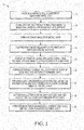
- FIG. 1 is a flowchart showing an example embodiment of a procedure 10 for fabricating a capacitive humidity sensor on an integrated circuit (IC) substrate according to example embodiments of the present disclosure.
- the procedure is a low-temperature process conducted at a maximum temperature of 300°C.
- Figs. 2 to 11 illustrate views of a semiconductor device at various stages of manufacture according to the process flow shown in FIG. 1 .
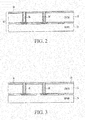
- the fabrication procedure 10 commences at block 12 where a substrate 30 ( FIG. 2 ) is provided.
- the substrate 30 can be the form of a complementary metal oxide semiconductor (CMOS) substrate 32 bonded to a microelectromechanical systems (MEMS) substrate 34.
- MEMS microelectromechanical systems
- the MEMS substrate 34 is absent.
- the CMOS substrate 32 is structured with an insulating layer 38 (e.g., silicon oxide, SiO) on an upper surface.
- the CMOS substrate 32 can include a plurality of conductive through-silicon vias (TSVs) 36 that extend therethrough.
- TSVs through-silicon vias
- the conductive TSVs can be formed, for example, from copper, using known methods.
- a conductive metal layer 40 is formed on the insulating layer 38 on the upper surface of the CMOS substrate 32, as illustrated in FIG. 3 .
- the metal layer 40 is electrically connected to one or more TSVs.
- the conductive metal layer 40 is an inert metal being chemically inert or unreactive to the reagents used in the composition (e.g., solvents, acidic component, etc.) in the electrografting process.
- the metal layer 40 functions as the bottom electrode of the capacitive humidity sensor.
- the conductive metal layer can be formed from titanium (Ti), platinum (Pt), gold (Au), or another electrically conductive material to which an organic material layer (e.g., polymer layer) can be attached through an electrografting procedure as further described herein.
- the conductive metal layer 40 is compatible with an aqueous acidic composition applied in the electrografting process to attach the organic polymer layer thereto.
- the conductive metal layer 40 can be formed by any appropriate processing technique (e.g., physical vapor deposition (PVD) or sputtering, etc.).
- PVD physical vapor deposition
- sputtering etc.
- the maximum temperature at which block 14 ( FIG. 1 ) is performed is 200°C.
- the operational sequence of the process of FIG. 1 progresses to block 16 where a patterned mask 42 ( FIG. 4 ) such as a photoresist or other type of patternable material that can be selectively removed, is formed over the conductive metal layer 40.
- the mask 42 includes openings exposing the areas 44 of the metal layer on which an organic layer (e.g., polymer layer) is to be electrografted, and one or more electrical contact areas 46 at an edge 46 of the substrate 32.
- the maximum temperature at which block 16 ( FIG. 1 ) should be performed is 120°C.
- an organic layer 48 is formed on the unmasked, exposed area 44 of the electrically conductive metal layer 40 by an electrografting process, as depicted in FIG. 5 .
- the organic layer 48 is a moisture sensitive, dielectric polymer layer.
- Electrografting generally refers to an electrochemically initiated chemical grafting process whereby an organic layer (e.g., polymer layer) is attached to a solid conducting substrate such as a metal layer.
- suitable polymers as the polymer layer 48 in a capacitive humidity sensor according to the disclosure which have a sensitivity to water vapor (humidity)
- polyvinyl esters such as polyvinyl methacrylate (PVM), polyvinyl benzoate (PVG), polyvinyl crotonate (PVCr), polyvinyl cinnamate (PVCi), and polymethyl methacrylate (PMMA), among others.
- the polyvinyl ester polymer is polyvinyl benzoate, polyvinyl cinnamate and polyvinyl methacrylates.
- the polymer e.g., polyvinyl ester
- the polymer can incorporate functional groups such as carboxyl (-COOH), hydroxyl (-OH) or amino (-NH 2 ) groups, among others.
- Such substituents and/or functional groups provide cross-linking of polymer chains via dehydration, esterification, peptidation or other reaction involving the functional groups.
- a primer layer in a first step in the electrografting process, is chemically bonded to the exposed surface of the metal layer 40 to functionalize the metal layer with reactive groups.
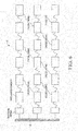
- the primer layer then initiates the polymerization of monomers (e.g., vinyl monomers) through the formation of initial primer-monomer bonds that will then anchor a network of polymer chains onto the surface of the metal layer 40, as illustrated in FIG. 6 .
- the electrografting process comprises electroreduction of an aryldiazonium salt or a vinyl compound in an aqueous acidic solution or in an organic solvent in the presence or absence of a cross-linking agent.
- a cross-linking agent e.g. divinyl benzene, ethylene glycol, etc.
- a cross-linking agent e.g. divinyl benzene, ethylene glycol, etc.
- desired cross-linking for example, of polymethyl methacrylate-type polymers.
- the organic solvent can be, for example, acetonitrile, dimethylformamide (DMF), propylene carbonates, dichloromethane, or other suitable organic solvents that fulfill both solubility and specific solvent potential window criteria for use in electrochemical processes including electrografting of aryldiazonium salts and vinyl compounds, among others.
- aryldiazonium salts include benzenediazonium, 4-carboxybenzenediazonium, 4-nitrobenzenediazonium, 4-acetamidobenzenediazonium, 4-bromobenzenediazonium, napthalenediazonium, and nitronapthalenediazonium, among others.
- vinyl compounds mentioned herein can be used for general electrografting purposes.
- suitable vinyl compounds include, for example, vinyl methacrylates (e.g. vinyl hydroxymethylmethacrylate, vinyl carboxymethylmethacrylate, vinyl aminomethylmethacrylate, etc.), vinyl benzoates (e.g. vinyl hydroxybenzoate, vinyl carboxybenzoate, vinyl aminobenzoate, etc.), vinyl cinnamates (e.g.
- (meth)acrylates e.g., butyl methacrylate, hydroxymethyl methacrylate, etc.
- ethyl acrylates e.g., 2 chloropropionate ethyl acetate, etc.
- the electrografting composition includes an inorganic acid such as hydrochloric acid (HCl), sulfuric acid (H 2 SO 4 ), and phosphoric acid (H 3 PO 4 ), among others.
- the amount of acid included in the solution is sufficient to provide an acidic condition for stability of diazonium salts in an aqueous solution.
- the amount of acid in the solution is sufficient to provide a pH in the range of 1 to 2.
- the electrografting composition is an aqueous solution comprising water, a vinyl monomer, an aryldiazonium cation, an inorganic acid (e.g., HCl or H 2 SO 4 ).
- the electrografting composition is an aqueous solution comprising water, 0.3 to 0.7 M vinyl monomer, 0.01 to 0.02 M aryldiazonium cation, and 0.01 to 0.1 M inorganic acid (e.g., HCl or H 2 SO 4 ). Electrografting process will be performed on the exposed area 44 of the metal layer 40 on the assembly shown in the FIGS. 4 and 5 .
- An electrochemical cell for carrying out this electrografting process will be composed of (i) a working electrode, which in the illustrated example embodiment, is the metal layer 40 (including the whole assembly as shown in the FIG. 5 ), (ii) a counter electrode of inert platinum (Pt) or suitable platinized metal (an external system to complete the electric circuit for electrografting; not a component of the assembly shown in FIG. 5 ), (iii) the electrografting solution applied between the working and the counter electrode, and (iv) an external power supply providing desired electrical potentials to the metal layer 40 (working electrode) through contact points 46 and to the external counter electrode (Pt or platinized metal).
- a working electrode which in the illustrated example embodiment, is the metal layer 40 (including the whole assembly as shown in the FIG. 5 ), (ii) a counter electrode of inert platinum (Pt) or suitable platinized metal (an external system to complete the electric circuit for electrografting; not a component of the assembly shown in FIG. 5 ), (iii) the electrografting
- the electrografting solution/composition can be prepared by mixing individual components (e.g., vinyl monomer, aryldiazonium cation and acidic components) in a dedicated mixing system (e.g., mixing chamber, beaker, etc.).
- a dedicated mixing system e.g., mixing chamber, beaker, etc.
- the electrografting composition can then be applied between the working and counter electrodes by using appropriate transfer system (e.g., beaker, other transfer vessel or apparatus).
- the electrografting process can be conducted by applying a desired potential (using an external power supply) for a specific period of time across the working and counter electrodes through the electrografting composition or solution (e.g ., containing vinyl monomer, aryldiazonium cation and acidic components), whereby electroreduction of the diazonium cation (ArN 2 + ) from the solution forms aryl radicals.
- a desired potential using an external power supply
- the electrografting composition or solution e.g containing vinyl monomer, aryldiazonium cation and acidic components
- Aryl radicals formed by the electroreduction of the diazonium salt from the solution chemically bond on one side to the surface of the metal layer 40 to form a primer layer (e.g., monolayer) of the aryl radicals, as illustrated in FIG. 6 .
- the aryl radicals initiate the polymerization of the vinyl compound which initially attach to the primer layer of aryl radicals.
- the polymerization reaction is continued to form the polymer layer 48.
- the electrografting reaction leads to a layer of the polyvinyl ester polymer on top of a primer layer bonded to the surface of the metal layer 40.
- the polymer layer can be rinsed to remove unattached polymer.
- the thickness of the polymer layer 48 can vary depending, for example, on the nature of the polymer, duration of the electrografting process, and on the specific use or purpose of the final device. In example embodiments, the polymer layer 48 ranges in thickness from 100 to 300 nm.
- the electrolysis can be performed by applying an electrical potential of -1V/SCE on the working electrode immersed in the electrografting solution.
- the applied voltage for electrolysis can vary depending, for example, on the nature/properties of the substrate metal (e.g ., reducibility or electron affinity), the dimension of the metal surface (e.g ., area or shape) to be electrografted, the type of diazonium and vinyl compounds, and also on the desired quality (e.g ., thickness, uniformity, etc.) of the grafted polymer film.
- the applied voltage will be different for each individual metals, e.g., Au, Ti and Cu, and also for various size and shape of the metal layer.
- the polymer layer 48 can then be annealed to achieve desired cross-linking and a re-organized polymer film with the desired thickness and uniformity.
- an anneal which is typically performed at a high temperature such as 100 to 300°C, can result in (i) cross-linking of polymers via chemical interaction of functional groups on adjacent chains, and/or (ii) physical re-organization of attached polymer chains via substantial change in molecular motions in the main polymer and side chains, removal of trapped solvents or gas, etc.
- the maximum temperature at which block 18 ( FIG. 1 ) should be annealed to form the polymer layer 48 is 250°C.
- the electrografting process provides a stable chemical bond between the electrically conductive metal layer 40 and the polymer layer 48.
- the resulting polymer layer 48 formed at the surface of the metal layer 40 can be detected, for example, by XPS and IR spectrographic techniques.
- the polymer layer 48 comprises a cross-linked polymer that is sensitive to water vapor.
- the water is absorbed into, or otherwise affects the polymer material resulting in an alteration in the permittivity (or dielectric constant) of the polymer material, which raises or lowers the capacitance of the capacitor.
- the amount of water vapor i.e., humidity
- a capacitive humidity sensor formed from a polyvinyl ester according to the disclosure can exhibit a relatively linear capacitance response over a range of 10% to 90% relative humidity.
- the operational sequence of FIG. 1 progresses to block 20 where exposed sections of the metal layer 40 are removed using the polymer layer 48 as a mask to expose the insulating layer 38 on the surface of the CMOS structure, as shown in FIG. 7 .
- the metal layer 40 can be removed, for example, by wet etching.
- the procedure of block 20 ( FIG. 1 ) can be performed at room temperature.
- an electrically conductive material layer is formed over the substrate, for example, by sputtering or other appropriate processing technique.
- the conductive material layer is then processed to form a redistribution layer (RDL) 50, is shown in FIG. 8 .
- the RDL layer 50 is generally composed of interconnects and other electrical contacts or pathways (e.g., traces, vias).
- the components of the RDL layer 50 can be formed using conventional substrate manufacturing processing, for example, patterning and etching.
- the RDL layer 50 can be formed, for example, from aluminum (Al), aluminum copper (AlCu), or another suitable electrically conductive material.
- the maximum temperature at which block 22 ( FIG. 12 ) should be performed is 200°C.
- an insulative layer 52 (also called a passivation layer or solder mask) is formed over the RDL layer 50, as shown in FIG. 9 .
- the insulative layer 52 is patterned to form one or more openings 54 to expose a contact area 56 of the RDL layer 50.
- the insulative layer 52 can be formed, for example, from a dielectric (insulating) material such as silicon dioxide, silicon nitride and silicon oxynitride, by any appropriate processing technique.
- the insulative layer 52 can be patterned and etched by a lithographic technique to expose active areas, traces and contacts of the RDL layer 50.
- the maximum temperature at which block 24 ( FIG. 1 ) should be performed is 300°C.
- electrically conductive materials e.g., metals
- the conductive materials are composed of three metal layers, for example, copper (Cu), nickel (Ni) and titanium (Ti).
- the conductive material layers can be deposited, for example, using a sputtering process.
- the maximum temperature at which block 26 ( FIG. 1 ) should be performed is 200°C.
- the UBM structure 58 is bowl-shaped with a depression therein. A solder ball (not shown) can be placed on top of the UBM structure such that, after reflow, the solder bump sits inside the UBM structure.
- one or more openings 60 are formed through the insulative (passivation) layer 52 and the underlying RDL layer 50, as shown in FIG. 11 , to expose the polymer layer 48 within a humidity sensing area 62 to the ambient air.
- the exposed polymer layer 48 which is composed of a moisture-sensitive polymer, functions as a capacitive humidity sensing element.
- the capacitive humidity sensor is composed of the moisture-sensitive polymer layer 48 (as the sensing element) situated between metal layer 40 as the bottom electrode and RDL layer 50 as the top electrode.
- the openings 60 can be formed, for example, by dry-etching the passivation layer 52 and wet-etching the RDL layer 50.
- the process of block 28 ( FIG. 1 ) can be performed at room temperature.
- the resulting semiconductor device 66 comprises a moisture-sensitive polymer layer 48 electrografted to an electrically conductive metal layer 40 situated on an IC substrate 30, and exposed within openings 62 through a passivation layer 52 and the RDL layer 50 such that the moisture-sensitive polymer layer 48 functions as a capacitive humidity sensor 64 when exposed to ambient air.
- the capacitive humidity sensor 64 is composed of the electrically conductive metal layer 40 as a bottom electrode and the RDL layer 50 as a top electrode.
- FIG. 12 is a flowchart showing an example embodiment of a second low-temperature procedure 110 for fabricating a capacitive humidity sensor on an integrated circuit (IC) substrate according to example embodiments of the present disclosure.
- Figs. 13 to 19 illustrate cross-sectional side views of a semiconductor device at various stages of manufacture according to the process flow shown in FIG. 12 .
- the procedure commences at block 112 where a substrate 130 ( FIG. 13 ) is provided.
- the substrate 130 can be in the form of a CMOS substrate 132 that is bonded to a MEMS substrate 134.
- the CMOS substrate 132 is structured with an insulating layer 138 (e.g., silicon oxide, SiO) on an upper surface.
- an insulating layer 138 e.g., silicon oxide, SiO
- the CMOS substrate 132 can include a plurality of conductive through-silicon vias (TSVs) 136 that extend through the CMOS substrate 132.
- TSVs through-silicon vias
- the MEMS substrate 134 is absent, and the capacitive humidity sensor can be fabricated using the CMOS substrate 132 as the substrate 130.
- an electrically conductive metal layer 140 is formed on the insulating layer 138 on the upper surface of the CMOS substrate 132, as shown in FIG. 13 , similar to the formation of metal layer 40 ( FIG. 3 ).
- the conductive metal layer 140 is a metal material (e.g Ti, Pt, Au, etc.) to which an organic material layer (e.g., polymer layer) can be attached through an electrografting process as described herein.
- the maximum temperature at which block 114 ( FIG. 13 ) should be performed is 200°C.
- the operational sequence 110 ( FIG. 12 ) progresses to block 115 where the conductive metal layer 140 is patterned into a pair of interdigitated sensing electrodes 147a, 147b, as shown in FIGS. 14 and 15 .
- the interdigitated sensing electrodes 147a, 147b are positioned in a humidity sensing region 162 of the CMOS substrate 132.
- the pair of sensing electrodes 147a, 147b are composed of two sets of interdigitated fingers or extensions.
- the set of fingers on a first side e.g., the left side
- the set of fingers on a second side e.g., the right side
- Sensing electrodes 147a, 147b function as opposite electrodes of the capacitor with the capacitance of the capacitor changing according to the humidity level.
- the metal layer 140 is also patterned such that electrically conductive contacts 146 are provided at each edge on the upper surface of the CMOS substrate 132.
- the electrical contacts 146 are connected to the metal layer 140 and provide a single electric potential to the sensing electrodes 147a, 147b for the electrografting process.
- the process of block 115 ( FIG. 12 ) can be performed at room temperature.
- the operational sequence 110 progresses to block 116 where a patterned mask 142 (e.g., photoresist, etc.) is formed over the conductive metal layer 140, as shown in FIG. 16 .
- the patterned mask 142 includes openings exposing the pair of interdigitated sensing electrodes 147a, 147b onto which an organic layer (e.g., polymer layer) is to be electrografted.
- the patterned mask (photoresist) layer 142 is applied such that at least a portion of the first and second electrical contact points 146 are left exposed at the edges of the substrate 130.
- the procedure of block 116 should be performed at a maximum temperature of 120°C.
- an organic (e.g., polymer) layer 148 is formed on the unmasked and exposed interdigitated sensing electrodes 147a, 147b by an electrografting process, as depicted in FIG. 17 .
- the polymer layer 148 comprises a cross-linked polymer that is sensitive to water vapor (humidity) whereby exposure to water vapor will alter the dielectric properties of the polymer material. By monitoring the change in capacitance, the relative humidity of the environment can be quantified.
- the electrografting process is performed on the exposed area of the sensing electrodes 147a, 147b on the assembly shown in FIG. 16 .
- An electrochemical cell for carrying out this electrografting process will be composed of (i) a working electrode, which in the illustrated example embodiment, is the sensing electrodes 147a, 147b of the metal layer 140 (including the whole assembly as shown in the FIG. 16 ).
- An electrochemical cell for carrying out this electrografting process will be composed of (i) a working electrode, which in the illustrated example embodiment, is the metal layer 40 (including the whole assembly as shown in the FIG.
- the electrografting solution/composition can be prepared by mixing the individual components (e.g., vinyl monomer, aryldiazonium cation and acidic components) in a dedicated mixing system (e.g., mixing chamber, beaker, etc.).
- a dedicated mixing system e.g., mixing chamber, beaker, etc.
- the electrografting composition can then be applied between the working and counter electrodes by using an appropriate transfer system (e.g., beaker or other transfer vessel or apparatus).
- the electrografting process can be conducted by applying a desired potential (using external power supply) for a specific period of time across the sensing (working) electrode 147a, 147b and the counter electrode through the electrografting composition (e.g., solution comprising vinyl compound, aryldiazonium salt, and the acidic components), whereby electroreduction of the diazonium cation (ArN 2 + ) from the solution forms aryl radicals.
- the aryl radicals chemically bond on one end to the surface of the sensing electrodes 147a, 147b to form a primer layer. On the other end, the aryl radicals initiate polymerization of the vinyl compound to form the polymer layer 148.
- the electrolysis can be performed by applying an electrical potential of -1V/SCE on the working electrode immersed in the electrografting solution.
- the applied voltage for electrolysis can vary depending, for example, on the nature/properties of the substrate metal (e.g ., reducibility or electron affinity), the dimension of the metal surface (e.g ., area or shape) to be electrografted, the type of diazonium and vinyl compounds, and also on the desired quality (e.g ., thickness, uniformity, etc.) of the grafted polymer film.
- the applied voltage will be different for each individual metals, e.g ., Au, Ti and Cu, and also for various size and shape of the metal layer.
- the polymer layer 148 can range in thickness from 10 to 1000 nm.
- the reaction leads to a layer of the polyvinyl ester polymer over a primer layer bonded to the surface of the metal layer 140.
- the polymer layer 148 can then be annealed to achieve desired cross-linking and a re-organized polymer film with the desired thickness and uniformity.
- an anneal which is typically performed at a high temperature such as 100 to 300°C, can result in (i) cross-linking of polymers via chemical interaction of functional groups on adjacent chains, and/or (ii) physical re-organization of attached polymer chains via substantial change in molecular motions in the main polymer and side chains, removal of trapped solvents or gas, etc.
- the polymer layer 148 comprises a humidity-sensitive polymer.
- the maximum temperature at which block 118 ( FIG. 12 ) should be performed is 250°C (for annealing the polymer layer).
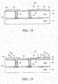
- the operational sequence of FIG. 12 progresses to block 122 wherein the photoresist mask is removed and a redistribution layer (RDL) 150 can be formed over the substrate, as shown in FIG. 18 .
- the RDL layer 150 can be formed, for example, by applying an electrically conductive material layer over the substrate (e.g., by sputtering or other processing technique) and then patterning (e.g., by wet etching) to form interconnects and other electrical contacts or pathways (e.g., traces, vias) as described with regard to FIG. 8 (block 22 of FIG. 1 ).
- the maximum temperature at which block 122 ( FIG. 12 ) should be performed is 200°C.
- an insulative layer 152 (e.g., a passivation layer) 52, as shown in FIG. 19 , is then formed over the substrate, and patterned to provide openings 154 to contact areas 156 of the RDL layer 150, and to expose the polymer layer 148 within the humidity sensing area 162.
- the insulative layer 152 e.g., passivation layer
- the maximum temperature at which block 124 ( FIG. 12 ) should be performed is 300°C.
- an under-bump metallization (UBM) structure 158 can be formed on the exposed contact area 156 of the RDL layer 150, as described with regard to FIG. 10 (block 26 of FIG. 1 ).
- a sputtering process can be used to deposit the metal layer for the UBM structure 158.
- the maximum temperature at which block 126 ( FIG. 12 ) should be performed is 200°C.
- a solder ball (not shown) can be mounted on the UBM structures.
- the resulting semiconductor device 166 comprises a moisture-sensitive polymer layer 148 electrografted to a pair of interdigitated sensing electrodes 147a, 147b of an electrically conductive metal layer 140 situated on an IC substrate 130, and exposed within an opening 154 in a passivation layer 152 such that the moisture-sensitive polymer layer 148 functions as a capacitive humidity sensor 164 when exposed to ambient air.
- FIGS. 1 and 12 are described in the context of capacitive humidity sensors, it should be understood that those procedures are also applicable to capacitive sensors that are configured for sensing chemical substances (e.g., gases) other than water vapor.
- a polymer for sensing a particular chemical or category of chemicals for example, sulfur oxides SO x (e.g., SO 2 , SO 3 , etc.), and gaseous nitrogen oxides NO x (e.g., NO, N 2 O, NO 2 , N 2 O 5 , etc.), is formed by electrografting according to the disclosure.
- polymers examples include, for example, polyvinyl methacrylates, polyvinyl benzoates, vinyl cinnamates, polyvinyl chrotonate, and polymethyl methacrylates, etc., as used for humidity sensors. Variations can be made in the cross-linked polymer structures (e.g., pore size, etc., specific for the physical absorption of gas molecules of particular size and shape) via suitable control of the number and nature of the functional groups on the polymer chain and thereby controlling interactions between the functional groups on adjacent polymer chains during a post-electrografting anneal step.
- cross-linked polymer structures e.g., pore size, etc., specific for the physical absorption of gas molecules of particular size and shape
- FIG. 21 illustrates another example embodiment of a capacitive humidity sensor 264 fabricated according to an example embodiment of the disclosure on a substrate 230 composed of an application-specific integrated circuit (ASIC), without TSVs or a MEMS substrate.
- the ASIC substrate 230 includes an insulating layer 238 and contact pads 233 on an upper surface.
- An electrically conductive metal layer 240 is formed over one of the contact pads 233 and a portion of the insulating layer 23 8.
- the metal layer 240 is then covered by a patterned mask (not shown) and an organic layer 248 (e.g., a moisture-sensitive polymer layer) is electrografted to an exposed area of the conductive metal layer 240 as described herein.
- an organic layer 248 e.g., a moisture-sensitive polymer layer
- a second electrically conductive material layer 250 is then formed over the substrate, a contact pad 233, and the polymer layer 248.
- the conductive material layer 250 is patterned (e.g., by etching) to form components of an RDL layer and openings 254 therethrough to expose the polymer layer 248.
- the resulting device 266 includes a capacitive humidity sensor 264 is composed of the moisture-sensitive polymer layer 248 exposed within the openings 254 to the ambient air within a humidity sensing region 262.
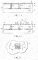
- an encapsulation process can be performed to cover the device 66 with a mold compound or mold encapsulant 68, which is then cured, to produce a semiconductor device package 70a, 70b.
- the semiconductor device package 70a, 70b includes the capacitive humidity sensor 64 formed on and exposed at the surface of an encapsulated IC substrate (e.g., CMOS, ASIC, etc.).
- the molding material can be any appropriate encapsulant, for example, a silica-filled epoxy molding compound, a plastic encapsulation resin, or other polymeric material such as silicones, polyimides, phenolics and polyurethanes. Encapsulation of the device 66 can be conducted, for example, by transfer molding, stencil printing, compression molding, and the like.
- a portion of the device 66 including the capacitive humidity sensor 64 is not covered by the mold compound/encapsulant 68.
- External contacts 72 e.g., solder bumps
- a substrate 74 such as a PCB or other external circuitry.
- the substrate 74 (e.g., PCB, etc.) is structured with an opening 76 extending therethrough through which the capacitive humidity sensor 64 is exposed to ambient air.
- an opening or gap 78 is provided between the surface 80 of the encapsulant 68 covering the device package 70b and the substrate 74 (e.g., PCB, etc.) such that the capacitive humidity sensor 64 is exposed to the ambient air through the opening or gap 78 along a side 82 of the package 70 mounted on the substrate 74 (e.g., PCB, etc.).
- devices and packages comprising the capacitive humidity sensor, and the methods of forming the capacitive humidity sensor, as described herein or otherwise encompassed herein can be used in networking systems, automotive systems, smart phones, agriculture monitoring systems, and other applications.
- FIG. 24 is a schematic diagram of an example embodiment of an electronic circuit 300 for reading a capacitive humidity sensor 302 according to the disclosure to determine a level of sensed ambient humidity. Digitizing the value of a capacitive sensor may involve generating a frequency that is inversely proportional to a capacitance C of the capacitive humidity sensor 302 and counting pulses over a fixed period of time to determine the frequency.
- an analog timer circuit 304 is used to generate an output signal 306 with a frequency F OUT .
- the analog timer circuit 304 operates from a voltage supply V DD 308 of 5 volts.
- a first capacitor C1 310 functions as a bypass, shunting any alternating current components on V DD 308 to ground.
- a second capacitor C2 312 also functions as a bypass, shunting any alternating current components on a control voltage CV terminal of the analog timer circuit 304 to ground.
- the frequency F OUT of the analog timer circuit 304 is inversely proportional to a capacitance C provided by the capacitive humidity sensor 302.
- a microcontroller 314 is configured to count pulses of the output signal 306 within a given period of time to calculate a frequency for F OUT .
- a first resistor R1 316 and a second resistor R2 318 function as a voltage divider and are selected based upon the capacitance provided by the capacitive humidity sensor 302.
- the frequency for F OUT is proportional to a level of humidity sensed by the capacitive humidity sensor 302.
- the values of C1 310 and C2 312 may each be approximately 0.1 microfarads
- the value of R1 316 may be approximately 56 kilohms
- the value of R2 318 may be approximately 470 kilohms
- the analog timer circuit 304 may be a 555 timer integrated circuit (IC).
- the circuit 300 of FIG. 23 is provided for illustrative purposes only, as any of various approaches may be used to read the capacitive humidity sensor 302.
- One characteristic of the circuit 300 of FIG. 23 is that there is no requirement for an analog-to-digital converter (ADC) or comparator in the microcontroller 314.
- ADC analog-to-digital converter
- a method for forming a semiconductor device is provided.
- a first electrically conductive metal layer is formed on a surface of an IC substrate.
- a moisture sensitive polymer layer is electrografted onto the first electrically conductive metal layer.
- a passivation layer is formed over the substrate with the polymer layer exposed through one or more openings in the passivation layer. The polymer layer functions as a capacitive humidity sensing element when exposed to ambient air.
- the electrografting comprises applying an aqueous acidic electrografting composition to a surface of the first electrically conductive metal layer.
- the composition comprises a solvent, an aryldiazonium salt, a vinyl ester monomer compound and an acidic component to maintain a pH of 1 to 2.
- the electrografting further comprises applying an electric potential to the surface of the metal layer to form a primer layer of aryl radicals, followed by addition and polymerization of vinyl monomers onto the primer layer to form an electrografted polymer layer on the surface of the metal layer.
- the polymer layer comprises a polyvinyl ester.
- the polyvinyl ester is selected from the group consisting of polyvinyl methacrylate (PVM), polyvinyl benzoate (PVG), polyvinyl crotonate (PVCr), polyvinyl cinnamate (PVCi), and polymethyl methacrylate (PMMA).
- the polyvinyl ester comprises functional groups selected from the group consisting of carboxyl ( COOH), hydroxyl ( OH) and amino (NH 2 ) groups.
- the first electrically conductive metal layer comprises a pair of interdigitated sensing electrodes, and the polymer layer is electrographed to the pair of sensing electrodes.
- the electrically conductive metal layer comprises a metal selected from the group consisting of titanium, platinum, and gold, and combinations thereof.
- the IC substrate comprises a CMOS substrate or an ASIC substrate.
- the IC substrate prior to electrografting the polymer layer, forming the first electrically conductive metal layer over an insulating layer on the substrate; and forming a patterned mask over the first electrically conductive metal layer.
- the polymer layer is electrographed onto an exposed area of the first electrically conductive metal layer.
- the mask and conductive metal layer underlying the mask is selectively removed to expose the insulating layer on the substrate.
- a second electrically conductive metal layer is formed over the insulating layer and the polymer layer.
- the second electrically conductive metal layer is patterned to form an RDL layer comprising a contact area.
- a passivation layer is formed over the RDL layer.
- An opening is formed through the passivation layer to expose the contact area of the RDL layer.
- a UBM structure is formed on the contact area within the opening.
- a plurality of openings is formed through the passivation layer and the RDL layer underlying the passivation layer to expose the polymer layer.
- the polymer layer functions as a capacitive humidity sensing element when exposed to ambient air.
- the first electrically conductive metal layer is formed over an insulating layer on the substrate.
- the first electrically conductive metal layer is masked and patterned to form a pair of interdigitated sensing electrodes.
- a patterned photoresist mask is formed over the substrate with the interdigitated sensing electrodes exposed.
- the polymer layer is electrographed onto the exposed interdigitated sensing electrodes.
- the mask is removed to expose the insulating layer on the substrate.
- a second electrically conductive metal layer is formed over the insulating layer and the polymer layer.
- the second electrically conductive metal layer is patterned to form an RDL layer comprising a contact area.
- a passivation layer is formed over the RDL layer and the polymer layer.
- An opening is formed through the passivation layer to expose the contact area of the RDL layer and the polymer layer.
- a UBM structure is formed on the contact area within the opening.
- the polymer layer functions as a capacitive humidity sensing element when exposed to ambient air.
- a second electrically conductive material layer is formed over the polymer layer.
- a passivation layer is formed over the second electrically conductive material layer.
- a one or more of openings is formed through the passivation layer and underlying second electrically conductive layer to expose the polymer layer.
- the polymer layer functions as a capacitive humidity sensing element when exposed to ambient air.
- a semiconductor device which comprises a moisture sensitive polymer layer electrografted to a first electrically conductive metal layer situated on an IC substrate, and exposed within one or more openings through a passivation layer.
- the moisture sensitive polymer layer functions as a capacitive humidity sensing element when exposed to ambient air.
- the moisture sensitive polymer layer is exposed within openings through the passivation layer and the RDL layer underlying the passivation layer.
- the moisture sensitive polymer layer is electrographed to a pair of interdigitated sensing electrodes, and exposed within one or more openings through the passivation layer.
- the semiconductor device further comprises an IC substrate comprising an insulative layer on an upper surface; the first electrically conductive metal layer over the insulative layer; the moisture sensitive polymer layer electrografted to the first electrically conductive metal layer; an RDL layer overlying portions of the moisture sensitive polymer layer; a passivation layer overlying the RDL layer; and openings extending through the passivation layer and underlying RDL layer with the polymer layer exposed within the openings to ambient air.
- the polymer layer functions as a capacitive humidity sensing element.
- an encapsulated semiconductor device package which comprises a semiconductor device and an encapsulant.
- the semiconductor device comprises a moisture sensitive polymer layer electrografted to an electrically conductive metal layer situated on an IC substrate and exposed within one or more openings in a passivation layer.
- the encapsulant surrounds the device except for the moisture sensitive polymer layer which is exposed within the one or more openings in the passivation layer.
- the moisture sensitive polymer layer functions as a capacitive humidity sensing element when exposed to ambient air.
- the encapsulated semiconductor device is mounted on a substrate, and the package includes an opening for passage of ambient air to the moisture sensitive polymer layer. According to an example, the opening extends through the substrate.
- the opening is situated along a side of the package as a space between the encapsulated semiconductor device and the substrate.
- top,” “bottom,” “upper,” “lower,” “over,” “under,” “overlying,” “underlying” and the like in the description and in the claims, if any, are used for descriptive purposes and not necessarily for describing permanent relative positions. It is understood that the terms so used are interchangeable under appropriate circumstances such that the example embodiments of the invention described herein are, for example, capable of operation in other orientations than those illustrated or otherwise described herein.
- the terms “a” or “an,” as used herein, are defined as one or more than one.
Landscapes
- Chemical & Material Sciences (AREA)
- Engineering & Computer Science (AREA)
- Health & Medical Sciences (AREA)
- General Physics & Mathematics (AREA)
- Electrochemistry (AREA)
- Life Sciences & Earth Sciences (AREA)
- Analytical Chemistry (AREA)
- Biochemistry (AREA)
- General Health & Medical Sciences (AREA)
- Physics & Mathematics (AREA)
- Immunology (AREA)
- Pathology (AREA)
- Chemical Kinetics & Catalysis (AREA)
- Manufacturing & Machinery (AREA)
- Microelectronics & Electronic Packaging (AREA)
- Computer Hardware Design (AREA)
- Power Engineering (AREA)
- Investigating Or Analyzing Materials By The Use Of Electric Means (AREA)
Abstract
Description
- The present disclosure relates generally to structures for chemical sensing and, more particularly, to a capacitive humidity sensor integrated, for example, into a complementary metal oxide semiconductor (CMOS) substrate or like structure.
- In many automated industrial processes and climate control systems, it is often necessary to sense and control the ambient humidity level. Capacitive relative humidity sensors are widely used in various areas of applications such as instrumentation, automated systems and climatology, to monitor and detect humidity levels.
- Humidity sensors utilize changes in the physical and electrical properties of a sensitive material (e.g., dielectric polymer) when exposed to atmospheric humidity conditions of a surrounding area. In principle, with a capacitive type organic polymer film humidity sensor, the absorbed water vapor occupies free spaces between polymer molecules, and the dielectric permittivity of the polymer is linearly changed proportionally to the amount of absorbed water. Capacitive type humidity sensors thus provide a measure of the humidity based on the amount of absorption or desorption of water molecules and the resultant variation of the dielectric constant of the sensing material, and thus changes in its capacitance. Thus, humidity changes are directly detected by measuring the changes of the capacitance of the sensing material.
- In general, the typical configuration of a capacitance sensor is either a sandwich structure with two electrode surfaces on each side, or an interdigitated structure with comb electros and the sensing material (e.g., dielectric polymer) deposited inbetween.
- Various attempts have been made to integrate humidity and other chemical capacitance sensors into CMOS structures. For example, capacitive humidity sensors have been fabricated by forming a bottom electrode, depositing a chemical-sensitive polymer layer (e.g., polyimide), and then patterning a set of top electrodes (e.g., conductors). However, this structure is difficult to integrate with testing electronics. In addition, placing the sensitive material layer between two metal layers requires significant processing beyond conventional CMOS.
- Another attempt involved coating interdigitated metal electrodes with a chemical-sensitive polymer. While this approach eliminated the necessity of having metal above and below the sensitive layer, a large, parallel capacitance was created through the substrate under the electrodes.
- Another technique to produce an integrated chemical capacitance sensor into a CMOS structure involved selectively etching the dielectric of the CMOS to expose a core metal layer (electrically connected in series between two other metal adhesion layers). The exposed core metal layer is then etched to form a cavity between the two metal adhesion layers. The cavity is then filled with an environmental-sensitive dielectric material that is capable of selectively absorbing the chemical to be sensed. For humidity applications, polymers such as polyimide, polymethylmethacrylate (PMMA), poly(ethylene terephthalate (PET), polysulfone (PSF), cellulose acetate butyrate (CAB) and polyethynyl fluorenol (PEFI), are used. The metal adhesion layers then act as the top and bottom electrodes of the environmental-sensitive capacitor. However, this method requires the modification of the CMOS process flow to accommodate the incorporation of humidity sensor.
- Example embodiments of the present invention are illustrated by way of example and are not limited by the accompanying figures, in which like references indicate similar elements. Elements in the figures are illustrated for simplicity and clarity and have not necessarily been drawn to scale.
-
FIG. 1 is flow diagram illustrating a fabrication sequence to construct a capacitive humidity sensor according to an example embodiment of the invention, given by way of example. -
FIG. 2 is a cross-sectional, elevational view of an exemplary substrate for use in the procedure illustrated inFIG. 1 . -
FIG. 3 is a cross-sectional, elevational view of the substrate ofFIG. 2 , at a subsequent process step according to the operational sequence ofFIG. 1 , showing the deposition of an electrically conductive metal layer on the substrate. -
FIG. 4 is a cross-sectional, elevational view of the substrate ofFIG. 3 , at a subsequent process step according to the operational sequence ofFIG. 1 , showing the formation of a photomask onto the electrically conductive metal layer. -
FIG. 5 is a cross-sectional, elevational view of the substrate ofFIG. 4 , at a subsequent process step according to the operational sequence ofFIG. 1 , showing the formation of an organic (polymer) layer on the electrically conductive metal layer by an electrografting process. -
FIG. 6 is diagrammatic representation of an example embodiment of the configuration of an electrografted polymer attached to the electrically conductive metal layer. -
FIG. 7 is a cross-sectional, elevational view of the substrate ofFIG. 5 , at a subsequent process step according to the operational sequence ofFIG. 1 , showing the etched electrically conductive metal layer. -
FIG. 8 is a cross-sectional, elevational view of the substrate ofFIG. 7 , at a subsequent process step according to the operational sequence ofFIG. 1 , showing the formation of a redistribution layer (RDL). -
FIG. 9 is a cross-sectional, elevational view of the substrate ofFIG. 8 , at a subsequent process step according to the operational sequence ofFIG. 1 , showing the formation of a passivation layer over the RDL layer. -
FIG. 10 is a cross-sectional, elevational view of the substrate ofFIG. 9 , at a subsequent process step according to the operational sequence ofFIG. 1 , showing the formation of an under-bump metallization (UBM) structure. -
FIG. 11 is a cross-sectional, elevational view of the substrate ofFIG. 10 , at a subsequent process step according to the operational sequence ofFIG. 1 , showing the formation of openings to expose the polymer layer of the humidity sensor in the semiconductor device. -
FIG. 12 is flow diagram illustrating a fabrication sequence to construct a capacitive humidity sensor according to another example embodiment of the invention, given by way of example. -
FIG. 13 is a cross-sectional, elevational view of an exemplary substrate for use with the procedure illustrated inFIG. 12 , showing an electrically conductive metal layer formed on an insulative layer on the substrate. -
FIG. 14 is a cross-sectional, elevational view of the substrate ofFIG. 13 , at a subsequent process step according to the operational sequence ofFIG. 12 , showing the electrically conductive metal layer patterned to form a pair of interdigitated sensor electrodes. -
FIG. 15 is a top plan view of the interdigitated sensor electrodes ofFIG. 14 , taken along lines 15-15. -
FIG. 16 is a cross-sectional, elevational view of the substrate ofFIG. 14 , at a subsequent process step according to the operational sequence ofFIG. 12 , showing the formation of a patterned photoresist mask over portions of the electrically conductive metal layer and the substrate. -
FIG. 17 is a cross-sectional, elevational view of the substrate ofFIG. 16 , at a subsequent process step according to the operational sequence ofFIG. 12 , showing the formation of a polymer layer by electrografting on the unmasked portions of the interdigitated sensing electrodes. -
FIG. 18 is a cross-sectional, elevational view of the substrate ofFIG. 17 , at a subsequent process step according to the operational sequence ofFIG. 12 , showing removal of the mask and the formation of an RDL layer. -
FIG. 19 is a cross-sectional, elevational view of the substrate ofFIG. 18 , at a subsequent process step according to the operational sequence ofFIG. 12 , showing the formation of a passivation layer on portions of the RDL layer. -
FIG. 20 is a cross-sectional, elevational view of the substrate ofFIG. 19 , at a subsequent process step according to the operational sequence ofFIG. 12 , showing the formation of an under-bump metallization (UBM) structure, and the resulting device incorporating a capacitive humidity sensor. -
FIG. 21 is a cross-sectional, elevational view of a capacitive humidity sensor fabricated on an application-specific integrated circuit (ASIC) substrate according to another example embodiment of the disclosure. -
FIG. 22 is a cross-sectional, elevational view of an example embodiment of semiconductor device package according to the disclosure. -
FIG. 23 is a cross-sectional, elevational view of another example embodiment of semiconductor device package according to the disclosure. -
FIG. 24 is a schematic diagram of an illustrative electronic circuit for reading a capacitive humidity sensor to determine a level of sensed humidity. - Example embodiments of the disclosure generally include semiconductor devices, packaged devices, and methods for forming the devices and packages. The illustrated example embodiments correspond to the formation of semiconductor devices in the form of a CMOS device which is structured with a capacitive humidity sensor on an integrated circuit (IC) substrate (e.g., a CMOS substrate) according to various example embodiments of the disclosure. In example embodiments, the capacitive humidity sensor is formed by electrografting a moisture-sensitive polymer to a metal substrate layer.
- The present disclosure provides an improved method for integrating a capacitance-based humidity sensor into a CMOS structure using a post-CMOS approach. In addition, with the direct connection of MEM substrates to CMOS substrates through wafer bonding, example embodiments of the disclosure can be used to integrate humidity sensors onto such MEMS-CMOS substrates to achieve microsystems that have enhanced functionalities. Thus, in example embodiments, the disclosed process flows can integrate the fabrication of a humidity sensor on MEMS and CMOS substrates.
-
FIG. 1 is a flowchart showing an example embodiment of aprocedure 10 for fabricating a capacitive humidity sensor on an integrated circuit (IC) substrate according to example embodiments of the present disclosure. In example embodiments, the procedure is a low-temperature process conducted at a maximum temperature of 300°C.Figs. 2 to 11 illustrate views of a semiconductor device at various stages of manufacture according to the process flow shown inFIG. 1 . - The
fabrication procedure 10 commences atblock 12 where a substrate 30 (FIG. 2 ) is provided. As illustrated, in example embodiments, thesubstrate 30 can be the form of a complementary metal oxide semiconductor (CMOS)substrate 32 bonded to a microelectromechanical systems (MEMS)substrate 34. In another example embodiment, theMEMS substrate 34 is absent. As shown, theCMOS substrate 32 is structured with an insulating layer 38 (e.g., silicon oxide, SiO) on an upper surface. In example embodiments, theCMOS substrate 32 can include a plurality of conductive through-silicon vias (TSVs) 36 that extend therethrough. The conductive TSVs can be formed, for example, from copper, using known methods. Electrical contacts can then be made to the CMOS substrate through these TSVs. Next, at block 14 (FIG. 1 ), aconductive metal layer 40 is formed on the insulatinglayer 38 on the upper surface of theCMOS substrate 32, as illustrated inFIG. 3 . Themetal layer 40 is electrically connected to one or more TSVs. In example embodiments, theconductive metal layer 40 is an inert metal being chemically inert or unreactive to the reagents used in the composition (e.g., solvents, acidic component, etc.) in the electrografting process. In example embodiments, themetal layer 40 functions as the bottom electrode of the capacitive humidity sensor. - In various example embodiments, the conductive metal layer can be formed from titanium (Ti), platinum (Pt), gold (Au), or another electrically conductive material to which an organic material layer (e.g., polymer layer) can be attached through an electrografting procedure as further described herein. In various example embodiments, the
conductive metal layer 40 is compatible with an aqueous acidic composition applied in the electrografting process to attach the organic polymer layer thereto. Theconductive metal layer 40 can be formed by any appropriate processing technique (e.g., physical vapor deposition (PVD) or sputtering, etc.). In example embodiments, the maximum temperature at which block 14 (FIG. 1 ) is performed is 200°C. - The operational sequence of the process of
FIG. 1 progresses to block 16 where a patterned mask 42 (FIG. 4 ) such as a photoresist or other type of patternable material that can be selectively removed, is formed over theconductive metal layer 40. Themask 42 includes openings exposing theareas 44 of the metal layer on which an organic layer (e.g., polymer layer) is to be electrografted, and one or moreelectrical contact areas 46 at anedge 46 of thesubstrate 32. The maximum temperature at which block 16 (FIG. 1 ) should be performed is 120°C. - Next, at block 18 (
FIG. 1 ), anorganic layer 48 is formed on the unmasked, exposedarea 44 of the electricallyconductive metal layer 40 by an electrografting process, as depicted inFIG. 5 . In the illustrated example embodiment, theorganic layer 48 is a moisture sensitive, dielectric polymer layer. Electrografting generally refers to an electrochemically initiated chemical grafting process whereby an organic layer (e.g., polymer layer) is attached to a solid conducting substrate such as a metal layer. Examples of suitable polymers as thepolymer layer 48 in a capacitive humidity sensor according to the disclosure, which have a sensitivity to water vapor (humidity), include polyvinyl esters such as polyvinyl methacrylate (PVM), polyvinyl benzoate (PVG), polyvinyl crotonate (PVCr), polyvinyl cinnamate (PVCi), and polymethyl methacrylate (PMMA), among others. In an example embodiment, the polyvinyl ester polymer is polyvinyl benzoate, polyvinyl cinnamate and polyvinyl methacrylates. In example embodiments, the polymer (e.g., polyvinyl ester) can incorporate functional groups such as carboxyl (-COOH), hydroxyl (-OH) or amino (-NH2) groups, among others. Such substituents and/or functional groups provide cross-linking of polymer chains via dehydration, esterification, peptidation or other reaction involving the functional groups. - In an example embodiment, in a first step in the electrografting process, a primer layer is chemically bonded to the exposed surface of the
metal layer 40 to functionalize the metal layer with reactive groups. The primer layer then initiates the polymerization of monomers (e.g., vinyl monomers) through the formation of initial primer-monomer bonds that will then anchor a network of polymer chains onto the surface of themetal layer 40, as illustrated inFIG. 6 . - In various example embodiments, the electrografting process comprises electroreduction of an aryldiazonium salt or a vinyl compound in an aqueous acidic solution or in an organic solvent in the presence or absence of a cross-linking agent. For example, with a polyvinyl ester such as polyvinylbenzoate, polyvinyl cinnamate, and polyvinyl chrotonate, among others, which have carboxyl (-COOH), hydroxyl (-OH) and/or amino (-NH2) functional groups on adjacent polymer chains, internal cross-linking can occur during a post-electrografting anneal without the use of an added cross-linking agent. In other example embodiments, a cross-linking agent (e.g. divinyl benzene, ethylene glycol, etc.) can be added to the composition to introduce desired cross-linking, for example, of polymethyl methacrylate-type polymers.
- In various example embodiments, the organic solvent can be, for example, acetonitrile, dimethylformamide (DMF), propylene carbonates, dichloromethane, or other suitable organic solvents that fulfill both solubility and specific solvent potential window criteria for use in electrochemical processes including electrografting of aryldiazonium salts and vinyl compounds, among others. Examples of aryldiazonium salts include benzenediazonium, 4-carboxybenzenediazonium, 4-nitrobenzenediazonium, 4-acetamidobenzenediazonium, 4-bromobenzenediazonium, napthalenediazonium, and nitronapthalenediazonium, among others.
- In general, all vinyl compounds mentioned herein can be used for general electrografting purposes. For application in humidity sensors, suitable vinyl compounds include, for example, vinyl methacrylates (e.g. vinyl hydroxymethylmethacrylate, vinyl carboxymethylmethacrylate, vinyl aminomethylmethacrylate, etc.), vinyl benzoates (e.g. vinyl hydroxybenzoate, vinyl carboxybenzoate, vinyl aminobenzoate, etc.), vinyl cinnamates (e.g. vinyl hydroxycinnamate, vinyl carboxycinnamate, vinyl aminocinnamate, etc.), vinyl chrotonate, (meth)acrylates (e.g., butyl methacrylate, hydroxymethyl methacrylate, etc.), and ethyl acrylates (e.g., 2 chloropropionate ethyl acetate, etc.).
- In example embodiments, the electrografting composition includes an inorganic acid such as hydrochloric acid (HCl), sulfuric acid (H2SO4), and phosphoric acid (H3PO4), among others. In example embodiments, the amount of acid included in the solution is sufficient to provide an acidic condition for stability of diazonium salts in an aqueous solution. In example embodiments, the amount of acid in the solution is sufficient to provide a pH in the range of 1 to 2.
- In various example embodiments, the electrografting composition is an aqueous solution comprising water, a vinyl monomer, an aryldiazonium cation, an inorganic acid (e.g., HCl or H2SO4). In an example embodiment, the electrografting composition is an aqueous solution comprising water, 0.3 to 0.7 M vinyl monomer, 0.01 to 0.02 M aryldiazonium cation, and 0.01 to 0.1 M inorganic acid (e.g., HCl or H2SO4). Electrografting process will be performed on the exposed
area 44 of themetal layer 40 on the assembly shown in theFIGS. 4 and 5 . An electrochemical cell for carrying out this electrografting process will be composed of (i) a working electrode, which in the illustrated example embodiment, is the metal layer 40 (including the whole assembly as shown in theFIG. 5 ), (ii) a counter electrode of inert platinum (Pt) or suitable platinized metal (an external system to complete the electric circuit for electrografting; not a component of the assembly shown inFIG. 5 ), (iii) the electrografting solution applied between the working and the counter electrode, and (iv) an external power supply providing desired electrical potentials to the metal layer 40 (working electrode) through contact points 46 and to the external counter electrode (Pt or platinized metal). - In an example embodiment, the electrografting solution/composition can be prepared by mixing individual components (e.g., vinyl monomer, aryldiazonium cation and acidic components) in a dedicated mixing system (e.g., mixing chamber, beaker, etc.). The electrografting composition can then be applied between the working and counter electrodes by using appropriate transfer system (e.g., beaker, other transfer vessel or apparatus).
- In example embodiments, the electrografting process can be conducted by applying a desired potential (using an external power supply) for a specific period of time across the working and counter electrodes through the electrografting composition or solution (e.g., containing vinyl monomer, aryldiazonium cation and acidic components), whereby electroreduction of the diazonium cation (ArN2 +) from the solution forms aryl radicals.
- Aryl radicals formed by the electroreduction of the diazonium salt from the solution, chemically bond on one side to the surface of the
metal layer 40 to form a primer layer (e.g., monolayer) of the aryl radicals, as illustrated inFIG. 6 . On the other side, the aryl radicals initiate the polymerization of the vinyl compound which initially attach to the primer layer of aryl radicals. The polymerization reaction is continued to form thepolymer layer 48. In example embodiments, the electrografting reaction leads to a layer of the polyvinyl ester polymer on top of a primer layer bonded to the surface of themetal layer 40. In example embodiments, the polymer layer can be rinsed to remove unattached polymer. The thickness of thepolymer layer 48 can vary depending, for example, on the nature of the polymer, duration of the electrografting process, and on the specific use or purpose of the final device. In example embodiments, thepolymer layer 48 ranges in thickness from 100 to 300 nm. - The electrolysis can be performed by applying an electrical potential of -1V/SCE on the working electrode immersed in the electrografting solution. The applied voltage for electrolysis can vary depending, for example, on the nature/properties of the substrate metal (e.g., reducibility or electron affinity), the dimension of the metal surface (e.g., area or shape) to be electrografted, the type of diazonium and vinyl compounds, and also on the desired quality (e.g., thickness, uniformity, etc.) of the grafted polymer film. For example, the applied voltage will be different for each individual metals, e.g., Au, Ti and Cu, and also for various size and shape of the metal layer.
- In example embodiments, the
polymer layer 48 can then be annealed to achieve desired cross-linking and a re-organized polymer film with the desired thickness and uniformity. For example, an anneal, which is typically performed at a high temperature such as 100 to 300°C, can result in (i) cross-linking of polymers via chemical interaction of functional groups on adjacent chains, and/or (ii) physical re-organization of attached polymer chains via substantial change in molecular motions in the main polymer and side chains, removal of trapped solvents or gas, etc. - In example embodiments, the maximum temperature at which block 18 (
FIG. 1 ) should be annealed to form thepolymer layer 48 is 250°C. The electrografting process provides a stable chemical bond between the electricallyconductive metal layer 40 and thepolymer layer 48. The resultingpolymer layer 48 formed at the surface of themetal layer 40 can be detected, for example, by XPS and IR spectrographic techniques. - In example embodiments, the
polymer layer 48 comprises a cross-linked polymer that is sensitive to water vapor. When thepolymer layer 48 is exposed to water vapor, the water is absorbed into, or otherwise affects the polymer material resulting in an alteration in the permittivity (or dielectric constant) of the polymer material, which raises or lowers the capacitance of the capacitor. By monitoring the change in capacitance, the amount of water vapor (i.e., humidity) can be quantified. In example embodiments, a capacitive humidity sensor formed from a polyvinyl ester according to the disclosure, can exhibit a relatively linear capacitance response over a range of 10% to 90% relative humidity. - After forming the
polymer layer 48, the operational sequence ofFIG. 1 progresses to block 20 where exposed sections of themetal layer 40 are removed using thepolymer layer 48 as a mask to expose the insulatinglayer 38 on the surface of the CMOS structure, as shown inFIG. 7 . Themetal layer 40 can be removed, for example, by wet etching. The procedure of block 20 (FIG. 1 ) can be performed at room temperature. - Next, at block 22 (
FIG. 1 ), an electrically conductive material layer is formed over the substrate, for example, by sputtering or other appropriate processing technique. The conductive material layer is then processed to form a redistribution layer (RDL) 50, is shown inFIG. 8 . TheRDL layer 50 is generally composed of interconnects and other electrical contacts or pathways (e.g., traces, vias). The components of theRDL layer 50 can be formed using conventional substrate manufacturing processing, for example, patterning and etching. In various example embodiments, theRDL layer 50 can be formed, for example, from aluminum (Al), aluminum copper (AlCu), or another suitable electrically conductive material. The maximum temperature at which block 22 (FIG. 12 ) should be performed is 200°C. - At block 24 (
FIG. 1 ), an insulative layer 52 (also called a passivation layer or solder mask) is formed over theRDL layer 50, as shown inFIG. 9 . As depicted, theinsulative layer 52 is patterned to form one ormore openings 54 to expose acontact area 56 of theRDL layer 50. Theinsulative layer 52 can be formed, for example, from a dielectric (insulating) material such as silicon dioxide, silicon nitride and silicon oxynitride, by any appropriate processing technique. Theinsulative layer 52 can be patterned and etched by a lithographic technique to expose active areas, traces and contacts of theRDL layer 50. The maximum temperature at which block 24 (FIG. 1 ) should be performed is 300°C. - Next, at block 26 (
FIG. 1 ), electrically conductive materials (e.g., metals) are deposited onto the exposedcontact area 56 of the RDL, and patterned to form an under-bump metallization (UBM)structure 58, as shown inFIG. 10 . In example embodiments, the conductive materials are composed of three metal layers, for example, copper (Cu), nickel (Ni) and titanium (Ti). The conductive material layers can be deposited, for example, using a sputtering process. The maximum temperature at which block 26 (FIG. 1 ) should be performed is 200°C. In example embodiments, theUBM structure 58 is bowl-shaped with a depression therein. A solder ball (not shown) can be placed on top of the UBM structure such that, after reflow, the solder bump sits inside the UBM structure. - At block 28 (
FIG. 1 ), one ormore openings 60 are formed through the insulative (passivation)layer 52 and theunderlying RDL layer 50, as shown inFIG. 11 , to expose thepolymer layer 48 within ahumidity sensing area 62 to the ambient air. The exposedpolymer layer 48, which is composed of a moisture-sensitive polymer, functions as a capacitive humidity sensing element. The capacitive humidity sensor is composed of the moisture-sensitive polymer layer 48 (as the sensing element) situated betweenmetal layer 40 as the bottom electrode andRDL layer 50 as the top electrode. - The
openings 60 can be formed, for example, by dry-etching thepassivation layer 52 and wet-etching theRDL layer 50. The process of block 28 (FIG. 1 ) can be performed at room temperature. - The resulting
semiconductor device 66 comprises a moisture-sensitive polymer layer 48 electrografted to an electricallyconductive metal layer 40 situated on anIC substrate 30, and exposed withinopenings 62 through apassivation layer 52 and theRDL layer 50 such that the moisture-sensitive polymer layer 48 functions as acapacitive humidity sensor 64 when exposed to ambient air. Thus, in some example embodiments, thecapacitive humidity sensor 64 is composed of the electricallyconductive metal layer 40 as a bottom electrode and theRDL layer 50 as a top electrode. -
FIG. 12 is a flowchart showing an example embodiment of a second low-temperature procedure 110 for fabricating a capacitive humidity sensor on an integrated circuit (IC) substrate according to example embodiments of the present disclosure.Figs. 13 to 19 illustrate cross-sectional side views of a semiconductor device at various stages of manufacture according to the process flow shown inFIG. 12 . The procedure commences atblock 112 where a substrate 130 (FIG. 13 ) is provided. As illustrated, in example embodiments, thesubstrate 130 can be in the form of aCMOS substrate 132 that is bonded to aMEMS substrate 134. As shown, theCMOS substrate 132 is structured with an insulating layer 138 (e.g., silicon oxide, SiO) on an upper surface. TheCMOS substrate 132 can include a plurality of conductive through-silicon vias (TSVs) 136 that extend through theCMOS substrate 132. In another example embodiment, theMEMS substrate 134 is absent, and the capacitive humidity sensor can be fabricated using theCMOS substrate 132 as thesubstrate 130. - Next, at block 114 (
FIG. 12 ), an electricallyconductive metal layer 140 is formed on the insulatinglayer 138 on the upper surface of theCMOS substrate 132, as shown inFIG. 13 , similar to the formation of metal layer 40 (FIG. 3 ). Theconductive metal layer 140 is a metal material (e.g Ti, Pt, Au, etc.) to which an organic material layer (e.g., polymer layer) can be attached through an electrografting process as described herein. The maximum temperature at which block 114 (FIG. 13 ) should be performed is 200°C. - The operational sequence 110 (
FIG. 12 ) progresses to block 115 where theconductive metal layer 140 is patterned into a pair of interdigitatedsensing electrodes FIGS. 14 and 15 . The interdigitatedsensing electrodes humidity sensing region 162 of theCMOS substrate 132. - As shown in
FIG. 15 , the pair ofsensing electrodes sensing electrode 147a, and the set of fingers on a second side (e.g., the right side) forms the other sensing electrode147b.Sensing electrodes - The
metal layer 140 is also patterned such that electricallyconductive contacts 146 are provided at each edge on the upper surface of theCMOS substrate 132. Theelectrical contacts 146 are connected to themetal layer 140 and provide a single electric potential to thesensing electrodes - The process of block 115 (
FIG. 12 ) can be performed at room temperature. - The operational sequence 110 (
FIG. 12 ) progresses to block 116 where a patterned mask 142 (e.g., photoresist, etc.) is formed over theconductive metal layer 140, as shown inFIG. 16 . The patternedmask 142 includes openings exposing the pair of interdigitatedsensing electrodes layer 142 is applied such that at least a portion of the first and second electrical contact points 146 are left exposed at the edges of thesubstrate 130. The procedure ofblock 116 should be performed at a maximum temperature of 120°C. - Next, at block 118 (
FIG. 12 ), an organic (e.g., polymer)layer 148 is formed on the unmasked and exposed interdigitatedsensing electrodes FIG. 17 . In example embodiments, thepolymer layer 148 comprises a cross-linked polymer that is sensitive to water vapor (humidity) whereby exposure to water vapor will alter the dielectric properties of the polymer material. By monitoring the change in capacitance, the relative humidity of the environment can be quantified. - In an example embodiment according to the disclosure, in a first step in an electrografting process, an aqueous acidic electrografting composition comprising water (as solvent), an aryldiazonium salt, a vinyl compound and an acidic component (to maintain pH = 1 to 2), as described with regard to
FIG. 5 (block 18 ofFIG. 1 is applied to the exposedelectrodes - In the illustrated example embodiment, the electrografting process is performed on the exposed area of the
sensing electrodes FIG. 16 . An electrochemical cell for carrying out this electrografting process will be composed of (i) a working electrode, which in the illustrated example embodiment, is thesensing electrodes FIG. 16 ). An electrochemical cell for carrying out this electrografting process will be composed of (i) a working electrode, which in the illustrated example embodiment, is the metal layer 40 (including the whole assembly as shown in theFIG. 5 ), (ii) a counter electrode of inert platinum (Pt) or suitable platinized metal (external system to complete the electric circuit for electrografting; not a component of the assembly shown inFIG. 5 ), (iii) the electrografting solution applied between the working and the counter electrode, and (iv) an external power supply providing desired electrical potentials to the metal layer 40 (working electrode) through contact points 46 and to the external counter electrode (Pt or platinized metal). - In an example embodiment, the electrografting solution/composition can be prepared by mixing the individual components (e.g., vinyl monomer, aryldiazonium cation and acidic components) in a dedicated mixing system (e.g., mixing chamber, beaker, etc.). The electrografting composition can then be applied between the working and counter electrodes by using an appropriate transfer system (e.g., beaker or other transfer vessel or apparatus).
- In example embodiments, the electrografting process can be conducted by applying a desired potential (using external power supply) for a specific period of time across the sensing (working)
electrode sensing electrodes polymer layer 148. - The electrolysis can be performed by applying an electrical potential of -1V/SCE on the working electrode immersed in the electrografting solution. The applied voltage for electrolysis can vary depending, for example, on the nature/properties of the substrate metal (e.g., reducibility or electron affinity), the dimension of the metal surface (e.g., area or shape) to be electrografted, the type of diazonium and vinyl compounds, and also on the desired quality (e.g., thickness, uniformity, etc.) of the grafted polymer film. For example, the applied voltage will be different for each individual metals, e.g., Au, Ti and Cu, and also for various size and shape of the metal layer.
- As the growth of the
polymer layer 148 proceeds around the surface of the interdigitatedelectrodes interdigitated electrodes polymer layer 148. In example embodiments, thepolymer layer 148 can range in thickness from 10 to 1000 nm. In example embodiments, the reaction leads to a layer of the polyvinyl ester polymer over a primer layer bonded to the surface of themetal layer 140. - In example embodiments, the
polymer layer 148 can then be annealed to achieve desired cross-linking and a re-organized polymer film with the desired thickness and uniformity. For example, as discussed above, an anneal, which is typically performed at a high temperature such as 100 to 300°C, can result in (i) cross-linking of polymers via chemical interaction of functional groups on adjacent chains, and/or (ii) physical re-organization of attached polymer chains via substantial change in molecular motions in the main polymer and side chains, removal of trapped solvents or gas, etc. In various example embodiments, thepolymer layer 148 comprises a humidity-sensitive polymer. In example embodiments, the maximum temperature at which block 118 (FIG. 12 ) should be performed is 250°C (for annealing the polymer layer). - After forming the
polymer layer 148, the operational sequence ofFIG. 12 progresses to block 122 wherein the photoresist mask is removed and a redistribution layer (RDL) 150 can be formed over the substrate, as shown inFIG. 18 . TheRDL layer 150 can be formed, for example, by applying an electrically conductive material layer over the substrate (e.g., by sputtering or other processing technique) and then patterning (e.g., by wet etching) to form interconnects and other electrical contacts or pathways (e.g., traces, vias) as described with regard toFIG. 8 (block 22 ofFIG. 1 ). The maximum temperature at which block 122 (FIG. 12 ) should be performed is 200°C. - At block 124 (
FIG. 12 ), an insulative layer 152 (e.g., a passivation layer) 52, as shown inFIG. 19 , is then formed over the substrate, and patterned to provideopenings 154 to contactareas 156 of theRDL layer 150, and to expose thepolymer layer 148 within thehumidity sensing area 162. The insulative layer 152 (e.g., passivation layer) can be formed and patterned as described with regard toFIG. 9 (block 24 ofFIG. 1 ). The maximum temperature at which block 124 (FIG. 12 ) should be performed is 300°C. - Next, at block 126 (
FIG. 12 ), an under-bump metallization (UBM)structure 158, as shown inFIG. 20 , can be formed on the exposedcontact area 156 of theRDL layer 150, as described with regard toFIG. 10 (block 26 ofFIG. 1 ). A sputtering process can be used to deposit the metal layer for theUBM structure 158. The maximum temperature at which block 126 (FIG. 12 ) should be performed is 200°C. In an example embodiment, a solder ball (not shown) can be mounted on the UBM structures. - The resulting
semiconductor device 166 comprises a moisture-sensitive polymer layer 148 electrografted to a pair of interdigitatedsensing electrodes conductive metal layer 140 situated on anIC substrate 130, and exposed within anopening 154 in apassivation layer 152 such that the moisture-sensitive polymer layer 148 functions as acapacitive humidity sensor 164 when exposed to ambient air. - Although the procedures of
FIGS. 1 and12 are described in the context of capacitive humidity sensors, it should be understood that those procedures are also applicable to capacitive sensors that are configured for sensing chemical substances (e.g., gases) other than water vapor. For these applications, a polymer for sensing a particular chemical or category of chemicals, for example, sulfur oxides SOx (e.g., SO2, SO3, etc.), and gaseous nitrogen oxides NOx (e.g., NO, N2O, NO2, N2O5, etc.), is formed by electrografting according to the disclosure. Examples of such polymers include, for example, polyvinyl methacrylates, polyvinyl benzoates, vinyl cinnamates, polyvinyl chrotonate, and polymethyl methacrylates, etc., as used for humidity sensors. Variations can be made in the cross-linked polymer structures (e.g., pore size, etc., specific for the physical absorption of gas molecules of particular size and shape) via suitable control of the number and nature of the functional groups on the polymer chain and thereby controlling interactions between the functional groups on adjacent polymer chains during a post-electrografting anneal step. -
FIG. 21 illustrates another example embodiment of acapacitive humidity sensor 264 fabricated according to an example embodiment of the disclosure on asubstrate 230 composed of an application-specific integrated circuit (ASIC), without TSVs or a MEMS substrate. As illustrated, theASIC substrate 230 includes an insulatinglayer 238 andcontact pads 233 on an upper surface. An electricallyconductive metal layer 240 is formed over one of thecontact pads 233 and a portion of the insulating layer 23 8. Themetal layer 240 is then covered by a patterned mask (not shown) and an organic layer 248 (e.g., a moisture-sensitive polymer layer) is electrografted to an exposed area of theconductive metal layer 240 as described herein. A second electricallyconductive material layer 250 is then formed over the substrate, acontact pad 233, and thepolymer layer 248. Theconductive material layer 250 is patterned (e.g., by etching) to form components of an RDL layer andopenings 254 therethrough to expose thepolymer layer 248. The resultingdevice 266 includes acapacitive humidity sensor 264 is composed of the moisture-sensitive polymer layer 248 exposed within theopenings 254 to the ambient air within ahumidity sensing region 262. - In example embodiments, as illustrated in
FIGS. 22 and 23 showing the semiconductor device 66 (FIG. 11 ) prepared according to the process ofFIG. 1 as an example, an encapsulation process can be performed to cover thedevice 66 with a mold compound ormold encapsulant 68, which is then cured, to produce asemiconductor device package semiconductor device package capacitive humidity sensor 64 formed on and exposed at the surface of an encapsulated IC substrate (e.g., CMOS, ASIC, etc.). The molding material can be any appropriate encapsulant, for example, a silica-filled epoxy molding compound, a plastic encapsulation resin, or other polymeric material such as silicones, polyimides, phenolics and polyurethanes. Encapsulation of thedevice 66 can be conducted, for example, by transfer molding, stencil printing, compression molding, and the like. - As shown in
FIGS. 22 and 23 , a portion of thedevice 66 including thecapacitive humidity sensor 64 is not covered by the mold compound/encapsulant 68. External contacts 72 (e.g., solder bumps) can be attached onto theUBM structures 58 of the device and mounted on asubstrate 74 such as a PCB or other external circuitry. - In the example embodiment of the
device package 70a shown inFIG. 22 , the substrate 74 (e.g., PCB, etc.) is structured with anopening 76 extending therethrough through which thecapacitive humidity sensor 64 is exposed to ambient air. In another example embodiment shown inFIG. 23 , an opening orgap 78 is provided between thesurface 80 of theencapsulant 68 covering thedevice package 70b and the substrate 74 (e.g., PCB, etc.) such that thecapacitive humidity sensor 64 is exposed to the ambient air through the opening orgap 78 along aside 82 of the package 70 mounted on the substrate 74 (e.g., PCB, etc.). - In various example embodiments, devices and packages comprising the capacitive humidity sensor, and the methods of forming the capacitive humidity sensor, as described herein or otherwise encompassed herein, can be used in networking systems, automotive systems, smart phones, agriculture monitoring systems, and other applications.
-
FIG. 24 is a schematic diagram of an example embodiment of anelectronic circuit 300 for reading acapacitive humidity sensor 302 according to the disclosure to determine a level of sensed ambient humidity. Digitizing the value of a capacitive sensor may involve generating a frequency that is inversely proportional to a capacitance C of thecapacitive humidity sensor 302 and counting pulses over a fixed period of time to determine the frequency. In the configuration ofFIG. 24 , ananalog timer circuit 304 is used to generate anoutput signal 306 with a frequency FOUT. Theanalog timer circuit 304 operates from avoltage supply V DD 308 of 5 volts. Afirst capacitor C1 310 functions as a bypass, shunting any alternating current components onV DD 308 to ground. Asecond capacitor C2 312 also functions as a bypass, shunting any alternating current components on a control voltage CV terminal of theanalog timer circuit 304 to ground. - The frequency FOUT of the
analog timer circuit 304 is inversely proportional to a capacitance C provided by thecapacitive humidity sensor 302. Amicrocontroller 314 is configured to count pulses of theoutput signal 306 within a given period of time to calculate a frequency for FOUT. Afirst resistor R1 316 and asecond resistor R2 318 function as a voltage divider and are selected based upon the capacitance provided by thecapacitive humidity sensor 302. The basic equation relating the capacitance C provided by the capacitive humidity sensor and frequency FOUT is: FOUT = 1/(C * (R1 + 2 * R2) * In 2). - The frequency for FOUT is proportional to a level of humidity sensed by the
capacitive humidity sensor 302. For illustrative purposes only, the values ofC1 310 andC2 312 may each be approximately 0.1 microfarads, the value ofR1 316 may be approximately 56 kilohms, the value ofR2 318 may be approximately 470 kilohms, and theanalog timer circuit 304 may be a 555 timer integrated circuit (IC). Thecircuit 300 ofFIG. 23 is provided for illustrative purposes only, as any of various approaches may be used to read thecapacitive humidity sensor 302. One characteristic of thecircuit 300 ofFIG. 23 is that there is no requirement for an analog-to-digital converter (ADC) or comparator in themicrocontroller 314. - According to an embodiment of the present application, a method for forming a semiconductor device is provided. A first electrically conductive metal layer is formed on a surface of an IC substrate. A moisture sensitive polymer layer is electrografted onto the first electrically conductive metal layer. A passivation layer is formed over the substrate with the polymer layer exposed through one or more openings in the passivation layer. The polymer layer functions as a capacitive humidity sensing element when exposed to ambient air.
- According to an example, the electrografting comprises applying an aqueous acidic electrografting composition to a surface of the first electrically conductive metal layer. The composition comprises a solvent, an aryldiazonium salt, a vinyl ester monomer compound and an acidic component to maintain a pH of 1 to 2. The electrografting further comprises applying an electric potential to the surface of the metal layer to form a primer layer of aryl radicals, followed by addition and polymerization of vinyl monomers onto the primer layer to form an electrografted polymer layer on the surface of the metal layer. According to an example, the polymer layer comprises a polyvinyl ester.
- According to an example, the polyvinyl ester is selected from the group consisting of polyvinyl methacrylate (PVM), polyvinyl benzoate (PVG), polyvinyl crotonate (PVCr), polyvinyl cinnamate (PVCi), and polymethyl methacrylate (PMMA). The polyvinyl ester comprises functional groups selected from the group consisting of carboxyl ( COOH), hydroxyl ( OH) and amino (NH2) groups. According to an example, the first electrically conductive metal layer comprises a pair of interdigitated sensing electrodes, and the polymer layer is electrographed to the pair of sensing electrodes.
- According to an example, the electrically conductive metal layer comprises a metal selected from the group consisting of titanium, platinum, and gold, and combinations thereof.
- According to an example, the IC substrate comprises a CMOS substrate or an ASIC substrate. According to an example, prior to electrografting the polymer layer, forming the first electrically conductive metal layer over an insulating layer on the substrate; and forming a patterned mask over the first electrically conductive metal layer. The polymer layer is electrographed onto an exposed area of the first electrically conductive metal layer.
- According to an example, after electrografting the polymer layer, the mask and conductive metal layer underlying the mask is selectively removed to expose the insulating layer on the substrate. A second electrically conductive metal layer is formed over the insulating layer and the polymer layer. The second electrically conductive metal layer is patterned to form an RDL layer comprising a contact area. A passivation layer is formed over the RDL layer. An opening is formed through the passivation layer to expose the contact area of the RDL layer. A UBM structure is formed on the contact area within the opening. A plurality of openings is formed through the passivation layer and the RDL layer underlying the passivation layer to expose the polymer layer. The polymer layer functions as a capacitive humidity sensing element when exposed to ambient air.
- According to an example, prior to electrografting the polymer layer, the first electrically conductive metal layer is formed over an insulating layer on the substrate. The first electrically conductive metal layer is masked and patterned to form a pair of interdigitated sensing electrodes. A patterned photoresist mask is formed over the substrate with the interdigitated sensing electrodes exposed. The polymer layer is electrographed onto the exposed interdigitated sensing electrodes.
- According to an example, after electrografting the polymer layer, the mask is removed to expose the insulating layer on the substrate. A second electrically conductive metal layer is formed over the insulating layer and the polymer layer. The second electrically conductive metal layer is patterned to form an RDL layer comprising a contact area. A passivation layer is formed over the RDL layer and the polymer layer. An opening is formed through the passivation layer to expose the contact area of the RDL layer and the polymer layer. A UBM structure is formed on the contact area within the opening. The polymer layer functions as a capacitive humidity sensing element when exposed to ambient air. According to an example, after electrografting the polymer layer, a second electrically conductive material layer is formed over the polymer layer. A passivation layer is formed over the second electrically conductive material layer. A one or more of openings is formed through the passivation layer and underlying second electrically conductive layer to expose the polymer layer. The polymer layer functions as a capacitive humidity sensing element when exposed to ambient air.
- According to an embodiment of the present application, a semiconductor device is provided, which comprises a moisture sensitive polymer layer electrografted to a first electrically conductive metal layer situated on an IC substrate, and exposed within one or more openings through a passivation layer. The moisture sensitive polymer layer functions as a capacitive humidity sensing element when exposed to ambient air.
- According to an example, the moisture sensitive polymer layer is exposed within openings through the passivation layer and the RDL layer underlying the passivation layer.
- According to an example, the moisture sensitive polymer layer is electrographed to a pair of interdigitated sensing electrodes, and exposed within one or more openings through the passivation layer. According to an example, the semiconductor device further comprises an IC substrate comprising an insulative layer on an upper surface; the first electrically conductive metal layer over the insulative layer; the moisture sensitive polymer layer electrografted to the first electrically conductive metal layer; an RDL layer overlying portions of the moisture sensitive polymer layer; a passivation layer overlying the RDL layer; and openings extending through the passivation layer and underlying RDL layer with the polymer layer exposed within the openings to ambient air. The polymer layer functions as a capacitive humidity sensing element.
- According to an embodiment of the present application, an encapsulated semiconductor device package is provided, which comprises a semiconductor device and an encapsulant. The semiconductor device comprises a moisture sensitive polymer layer electrografted to an electrically conductive metal layer situated on an IC substrate and exposed within one or more openings in a passivation layer. The encapsulant surrounds the device except for the moisture sensitive polymer layer which is exposed within the one or more openings in the passivation layer. The moisture sensitive polymer layer functions as a capacitive humidity sensing element when exposed to ambient air.
- According to an example, the encapsulated semiconductor device is mounted on a substrate, and the package includes an opening for passage of ambient air to the moisture sensitive polymer layer. According to an example, the opening extends through the substrate.
- According to an example, the opening is situated along a side of the package as a space between the encapsulated semiconductor device and the substrate.
- The terms "top," "bottom," "upper," "lower," "over," "under," "overlying," "underlying" and the like in the description and in the claims, if any, are used for descriptive purposes and not necessarily for describing permanent relative positions. It is understood that the terms so used are interchangeable under appropriate circumstances such that the example embodiments of the invention described herein are, for example, capable of operation in other orientations than those illustrated or otherwise described herein. The terms "a" or "an," as used herein, are defined as one or more than one. Also, the use of introductory phrases such as "at least one," "at least two," and "one or more" in the claims should not be construed to imply that the introduction of another claim element by the indefinite articles "a" or "an" limits any particular claim containing such introduced claim element to devices, etc., containing only one such element, even when the same claim includes the introductory phrases "one or more" or "at least one" and indefinite articles such as "a" or "an." The same applies to the use of definite articles.
- Although the invention is described herein with reference to specific example embodiments, various modifications and changes can be made without departing from the scope of the present invention as set forth in the claims below. Accordingly, the specification and figures are to be regarded in an illustrative rather than a restrictive sense, and all such modifications are intended to be included within the scope of the present invention. Any benefits, advantages, or solutions to problems that are described herein with regard to specific example embodiments are not intended to be construed as a critical, required or essential feature or element of any or all of the claims.
Claims (16)
the polyvinyl ester comprises functional groups selected from the group consisting of carboxyl (-COOH), hydroxyl (-OH) and amino (-NH2) groups.
forming (14) the first electrically conductive metal layer over an insulating layer (38) on the substrate; and
forming (16) a patterned mask (42) over the first electrically conductive metal layer;
wherein the polymer layer is electrographed onto an exposed area of the first electrically conductive metal layer.
selectively removing (20) the mask and conductive metal layer underlying the mask to expose the insulating layer on the substrate;
forming (22) a second electrically conductive metal layer over the insulating layer and the polymer layer;
patterning (22) the second electrically conductive metal layer to form an RDL layer (50) comprising a contact area (56);
forming (24) a passivation layer (52) over the RDL layer;
forming (28) an opening (54) through the passivation layer to expose the contact area of the RDL layer;
forming (28) a UBM structure (58) on the contact area within the opening; and
forming a plurality of openings (60, 76, 78) through the passivation layer and the RDL layer underlying the passivation layer to expose the polymer layer;
wherein the polymer layer functions as a capacitive humidity sensing element when exposed to ambient air.
forming (114) the first electrically conductive metal layer over an insulating layer (138) on the substrate; and
masking and patterning (115) the first electrically conductive metal layer to form a pair of interdigitated sensing electrodes; and
forming (116) a patterned photoresist mask (142) over the substrate with the interdigitated sensing electrodes exposed;
wherein the polymer layer is electrographed onto the exposed interdigitated sensing electrodes.
removing (122) the mask to expose the insulating layer on the substrate;
forming (122) a second electrically conductive metal layer over the insulating layer and the polymer layer;
patterning (122) the second electrically conductive metal layer to form an RDL layer (152) comprising a contact area (156);
forming a passivation layer (152) over the RDL layer and the polymer layer;
forming an opening (154) through the passivation layer to expose the contact area of the RDL layer and the polymer layer; and
forming (126) a UBM structure (158) on the contact area within the opening;
wherein the polymer layer functions as a capacitive humidity sensing element when exposed to ambient air.
forming (22, 122) a second electrically conductive material layer over the polymer layer; forming (24, 124) a passivation layer (52, 152) over the second electrically conductive material layer; and
forming (28, 126) one or more of openings (60, 76, 78) through the passivation layer and underlying second electrically conductive layer to expose the polymer layer;
wherein the polymer layer functions as a capacitive humidity sensing element when exposed to ambient air.
Applications Claiming Priority (1)
| Application Number | Priority Date | Filing Date | Title |
|---|---|---|---|
| US15/053,456 US10336606B2 (en) | 2016-02-25 | 2016-02-25 | Integrated capacitive humidity sensor |
Publications (2)
| Publication Number | Publication Date |
|---|---|
| EP3211409A1 true EP3211409A1 (en) | 2017-08-30 |
| EP3211409B1 EP3211409B1 (en) | 2021-06-16 |
Family
ID=57995055
Family Applications (1)
| Application Number | Title | Priority Date | Filing Date |
|---|---|---|---|
| EP17154932.2A Active EP3211409B1 (en) | 2016-02-25 | 2017-02-07 | Integrated capacitive humidity sensor |
Country Status (3)
| Country | Link |
|---|---|
| US (1) | US10336606B2 (en) |
| EP (1) | EP3211409B1 (en) |
| CN (1) | CN107121461B (en) |
Cited By (2)
| Publication number | Priority date | Publication date | Assignee | Title |
|---|---|---|---|---|
| DE102022213533A1 (en) * | 2022-12-13 | 2024-06-13 | Robert Bosch Gesellschaft mit beschränkter Haftung | Electronic component in a chip-scale package and method for producing a micromechanical sensor in a chip-scale package with compensation of moisture influences |
| KR102694447B1 (en) * | 2024-05-02 | 2024-08-13 | 서울시립대학교 산학협력단 | Organic Electronic Nose Using Semi-Permeable Polymer Membrane And Method For Detecting Chemical Species Using The Same |
Families Citing this family (11)
| Publication number | Priority date | Publication date | Assignee | Title |
|---|---|---|---|---|
| JP6983490B2 (en) * | 2016-03-29 | 2021-12-17 | ローム株式会社 | Electronic components |
| US11385083B2 (en) * | 2018-12-07 | 2022-07-12 | Mohammad Kabany | Method for measuring and/or processing measured pressure and/or humidity values |
| CN209326840U (en) | 2018-12-27 | 2019-08-30 | 热敏碟公司 | Pressure sensor and pressure transmitter |
| CN113366305B (en) * | 2019-02-15 | 2024-08-23 | 国立研究开发法人产业技术综合研究所 | Humidity sensor |
| CN110108763A (en) * | 2019-04-29 | 2019-08-09 | 南京邮电大学 | A kind of Low Drift Temperature capacitance type humidity sensor |
| CN111323459A (en) * | 2019-06-28 | 2020-06-23 | 福建师范大学 | Humidity sensor based on standard CMOS (complementary metal oxide semiconductor) process |
| CN110346423B (en) * | 2019-07-02 | 2021-05-04 | 杭州未名信科科技有限公司 | A CMOS-MEMS Humidity Sensor |
| US12130252B2 (en) * | 2019-11-04 | 2024-10-29 | Nutriprobe, Llc | Soil moisture and nutrient sensor system |
| US11573203B2 (en) * | 2020-09-21 | 2023-02-07 | Texas Instruments Incorporated | Humidity sensor |
| TWI741826B (en) * | 2020-10-12 | 2021-10-01 | 國立清華大學 | Sensing device, humidity sensing chip and method of manufacturing the device |
| EP4686696A1 (en) | 2024-07-31 | 2026-02-04 | STMicroelectronics International N.V. | Packaged mems device having a humidity sensor |
Citations (1)
| Publication number | Priority date | Publication date | Assignee | Title |
|---|---|---|---|---|
| US20140295605A1 (en) * | 2010-06-04 | 2014-10-02 | Carnegie Mellon University | Method of fabricating a capacitive environment sensor |
Family Cites Families (38)
| Publication number | Priority date | Publication date | Assignee | Title |
|---|---|---|---|---|
| US6724612B2 (en) * | 2002-07-09 | 2004-04-20 | Honeywell International Inc. | Relative humidity sensor with integrated signal conditioning |
| FR2843828A1 (en) * | 2002-08-26 | 2004-02-27 | Commissariat Energie Atomique | Support and selective coating procedure for conductive tracks e.g. on 'bio-chips', comprises using a polarization voltage shift system to select tracks |
| CN1210565C (en) * | 2003-06-12 | 2005-07-13 | 东南大学 | Miniature humidity sensor |
| US7053425B2 (en) * | 2003-11-12 | 2006-05-30 | General Electric Company | Gas sensor device |
| JP3994975B2 (en) * | 2004-02-27 | 2007-10-24 | 株式会社デンソー | Capacitive humidity sensor |
| WO2007036922A1 (en) * | 2005-09-30 | 2007-04-05 | Timothy Cummins | An integrated electronic sensor |
| US8357958B2 (en) * | 2004-04-02 | 2013-01-22 | Silicon Laboratories Inc. | Integrated CMOS porous sensor |
| EP1730506B1 (en) * | 2004-04-02 | 2018-09-26 | Silicon Laboratories Inc. | An integrated electronic sensor |
| DE102004027094A1 (en) * | 2004-06-02 | 2005-12-29 | Infineon Technologies Ag | Semiconductor module with a semiconductor sensor chip and a plastic housing and method for its production |
| JP4341506B2 (en) * | 2004-08-20 | 2009-10-07 | 株式会社デンソー | Hybrid sensor with humidity sensor and humidity detection function |
| CN1327215C (en) * | 2005-03-08 | 2007-07-18 | 东南大学 | Relative humidity sensor compatible of CMOS process |
| JP4609173B2 (en) * | 2005-04-22 | 2011-01-12 | 株式会社デンソー | Capacitive humidity sensor and manufacturing method thereof |
| JP5175974B2 (en) * | 2009-03-31 | 2013-04-03 | アルプス電気株式会社 | Capacitive humidity sensor and manufacturing method thereof |
| TWI474447B (en) * | 2009-06-29 | 2015-02-21 | 日月光半導體製造股份有限公司 | Semiconductor package structure and packaging method thereof |
| CN101620197B (en) * | 2009-07-23 | 2012-09-05 | 东南大学 | Rapid response CMOS relative humidity sensor |
| US20110088456A1 (en) * | 2009-10-16 | 2011-04-21 | Fan Ren | Normalized hydrogen sensing and methods of fabricating a normalized hydrogen sensor |
| US8610180B2 (en) * | 2010-06-11 | 2013-12-17 | Semiconductor Energy Laboratory Co., Ltd. | Gas sensor and method for manufacturing the gas sensor |
| WO2012046501A1 (en) * | 2010-10-04 | 2012-04-12 | アルプス電気株式会社 | Humidity detection sensor and process for production thereof |
| FR2971851A1 (en) * | 2011-02-22 | 2012-08-24 | Commissariat Energie Atomique | PROCESS FOR PRODUCING A BIOSENSOR |
| EP2492239B1 (en) * | 2011-02-22 | 2020-08-26 | Sciosense B.V. | Integrated circuit with sensor and method of manufacturing such an integrated circuit |
| JP5488534B2 (en) * | 2011-06-06 | 2014-05-14 | 株式会社デンソー | Humidity sensor and manufacturing method thereof |
| DE102011086479A1 (en) * | 2011-11-16 | 2013-05-16 | Robert Bosch Gmbh | Integrated humidity sensor and method for its production |
| JP5710538B2 (en) * | 2012-04-06 | 2015-04-30 | 日立オートモティブシステムズ株式会社 | Flow sensor |
| EP2657691B1 (en) * | 2012-04-25 | 2018-08-29 | E+E Elektronik Ges.m.b.H. | Moisture sensor assembly |
| EP2674392B1 (en) * | 2012-06-12 | 2017-12-27 | ams international AG | Integrated circuit with pressure sensor and manufacturing method |
| EP2693207A1 (en) * | 2012-07-30 | 2014-02-05 | Nxp B.V. | Integrated circuit comprising a capacitive gas sensor |
| EP2706567A1 (en) * | 2012-09-11 | 2014-03-12 | Nxp B.V. | Integrated circuit including an environmental sensor |
| EP2755023B1 (en) | 2013-01-11 | 2017-06-21 | MEAS France | Capacitive sensor integrated onto semiconductor circuit |
| US9080928B2 (en) * | 2013-01-11 | 2015-07-14 | Nokia Technologies Oy | Apparatus and associated methods |
| US10107625B2 (en) * | 2013-01-22 | 2018-10-23 | MCube Inc. | Integrated inertial sensing device |
| US9264040B2 (en) | 2013-12-19 | 2016-02-16 | Freescale Semiconductor, Inc. | Low leakage CMOS cell with low voltage swing |
| CN104849325B (en) * | 2014-02-18 | 2018-02-27 | 无锡华润上华科技有限公司 | The MEMS humidity sensor compatible with CMOS technology and its manufacture method |
| CN104089990B (en) * | 2014-07-15 | 2016-08-24 | 合肥工业大学 | A kind of relative humidity sensor of single-chip integration porous silicon and preparation method thereof |
| US9637371B2 (en) * | 2014-07-25 | 2017-05-02 | Semiconductor Manufacturing International (Shanghai) Corporation | Membrane transducer structures and methods of manufacturing same using thin-film encapsulation |
| EP3043173B1 (en) * | 2015-01-09 | 2017-09-06 | Honeywell International Inc. | A humidity sensor |
| CN104634487B (en) * | 2015-02-16 | 2017-05-31 | 迈尔森电子(天津)有限公司 | Mems pressure sensor and forming method thereof |
| CN104634832B (en) * | 2015-02-28 | 2018-01-05 | 苏州工业园区纳米产业技术研究院有限公司 | CMOS MEMS capacitive humidity sensors and preparation method thereof |
| US9845236B2 (en) * | 2015-03-12 | 2017-12-19 | Taiwan Semiconductor Manufacturing Co., Ltd. | Monolithic MEMS platform for integrated pressure, temperature, and gas sensor |
-
2016
- 2016-02-25 US US15/053,456 patent/US10336606B2/en active Active
-
2017
- 2017-02-07 EP EP17154932.2A patent/EP3211409B1/en active Active
- 2017-02-24 CN CN201710105978.8A patent/CN107121461B/en not_active Expired - Fee Related
Patent Citations (1)
| Publication number | Priority date | Publication date | Assignee | Title |
|---|---|---|---|---|
| US20140295605A1 (en) * | 2010-06-04 | 2014-10-02 | Carnegie Mellon University | Method of fabricating a capacitive environment sensor |
Non-Patent Citations (3)
| Title |
|---|
| AURÉLIA CHARLOT ET AL: "Combination of electrografting and layer-by-layer deposition: an efficient way to tailor polymer coatings of (semi)-conductors", CHEMICAL COMMUNICATIONS - CHEMCOM., no. 44, 26 September 2007 (2007-09-26), pages 4656, XP055385142, ISSN: 1359-7345, DOI: 10.1039/b712130j * |
| CORNILA C ET AL: "Capacitive sensors in CMOS technology with polymer coating", SENSORS AND ACTUATORS B: CHEMICAL: INTERNATIONAL JOURNAL DEVOTED TO RESEARCH AND DEVELOPMENT OF PHYSICAL AND CHEMICAL TRANSDUCERS, ELSEVIER BV, NL, vol. 25, no. 1-3, 1 April 1995 (1995-04-01), pages 357 - 361, XP026903842, ISSN: 0925-4005, [retrieved on 19950401], DOI: 10.1016/0925-4005(95)85080-5 * |
| DANIEL BÉLANGER ET AL: "Electrografting: a powerful method for surface modification", CHEMICAL SOCIETY REVIEWS, vol. 40, no. 7, 1 January 2011 (2011-01-01), pages 3995, XP055167668, ISSN: 0306-0012, DOI: 10.1039/c0cs00149j * |
Cited By (2)
| Publication number | Priority date | Publication date | Assignee | Title |
|---|---|---|---|---|
| DE102022213533A1 (en) * | 2022-12-13 | 2024-06-13 | Robert Bosch Gesellschaft mit beschränkter Haftung | Electronic component in a chip-scale package and method for producing a micromechanical sensor in a chip-scale package with compensation of moisture influences |
| KR102694447B1 (en) * | 2024-05-02 | 2024-08-13 | 서울시립대학교 산학협력단 | Organic Electronic Nose Using Semi-Permeable Polymer Membrane And Method For Detecting Chemical Species Using The Same |
Also Published As
| Publication number | Publication date |
|---|---|
| EP3211409B1 (en) | 2021-06-16 |
| US10336606B2 (en) | 2019-07-02 |
| CN107121461B (en) | 2021-09-24 |
| US20170247247A1 (en) | 2017-08-31 |
| CN107121461A (en) | 2017-09-01 |
Similar Documents
| Publication | Publication Date | Title |
|---|---|---|
| EP3211409B1 (en) | Integrated capacitive humidity sensor | |
| EP2755023B1 (en) | Capacitive sensor integrated onto semiconductor circuit | |
| DE102020110790B4 (en) | Sensor devices with gas-permeable lids and associated manufacturing processes | |
| US5928968A (en) | Semiconductor pressure transducer structures and methods for making the same | |
| JPH08510598A (en) | Method of manufacturing surface micromechanical structure | |
| CN109690302A (en) | Humidity sensor | |
| EP2230507A1 (en) | Humidity or gas sensor | |
| WO2014033056A1 (en) | Sensor part | |
| US9395318B2 (en) | Electrochemical sensor device | |
| CN103698367A (en) | Heating type humidity sensor and manufacturing method thereof | |
| EP2282333B1 (en) | Integrated circuit comprising moisture sensor | |
| US11167981B2 (en) | Semiconductor device and method of producing a semiconductor device | |
| DE102016115532B4 (en) | A method of forming a protective coating for an encapsulated semiconductor device | |
| CN113651287A (en) | Thin film sensor and packaging method thereof | |
| JP5397333B2 (en) | Semiconductor device, sensor element, and method of manufacturing semiconductor device | |
| CN113131780A (en) | Transparent flexible self-driven sensing device and preparation method thereof | |
| CN114424055A (en) | Method for manufacturing multi-pixel gas microsensor with multiple sensing capabilities | |
| JP2001249099A (en) | Capacitive humidity sensor and humidity measuring device | |
| Kim et al. | A highly sensitive capacitive-type humidity sensor using customized polyimide film without hydrophobic elements | |
| US20260018551A1 (en) | Highly integrated environmental sensor | |
| Vitoria et al. | Micro sized interdigital capacitor for humidity detection based on agarose coating | |
| JP5692331B2 (en) | Sensor element and method for manufacturing semiconductor device | |
| Ellis et al. | Microelectronic moisture sensor from variable dielectric capacitances of polyimide film | |
| Suzuki | Integrated, Intelligent Sensor Fabrication Strategies for Environmental Monitoring | |
| KR20190035989A (en) | Gas sensor package |
Legal Events
| Date | Code | Title | Description |
|---|---|---|---|
| PUAI | Public reference made under article 153(3) epc to a published international application that has entered the european phase |
Free format text: ORIGINAL CODE: 0009012 |
|
| STAA | Information on the status of an ep patent application or granted ep patent |
Free format text: STATUS: THE APPLICATION HAS BEEN PUBLISHED |
|
| AK | Designated contracting states |
Kind code of ref document: A1 Designated state(s): AL AT BE BG CH CY CZ DE DK EE ES FI FR GB GR HR HU IE IS IT LI LT LU LV MC MK MT NL NO PL PT RO RS SE SI SK SM TR |
|
| AX | Request for extension of the european patent |
Extension state: BA ME |
|
| STAA | Information on the status of an ep patent application or granted ep patent |
Free format text: STATUS: REQUEST FOR EXAMINATION WAS MADE |
|
| 17P | Request for examination filed |
Effective date: 20180228 |
|
| RBV | Designated contracting states (corrected) |
Designated state(s): AL AT BE BG CH CY CZ DE DK EE ES FI FR GB GR HR HU IE IS IT LI LT LU LV MC MK MT NL NO PL PT RO RS SE SI SK SM TR |
|
| STAA | Information on the status of an ep patent application or granted ep patent |
Free format text: STATUS: EXAMINATION IS IN PROGRESS |
|
| 17Q | First examination report despatched |
Effective date: 20190123 |
|
| GRAP | Despatch of communication of intention to grant a patent |
Free format text: ORIGINAL CODE: EPIDOSNIGR1 |
|
| STAA | Information on the status of an ep patent application or granted ep patent |
Free format text: STATUS: GRANT OF PATENT IS INTENDED |
|
| INTG | Intention to grant announced |
Effective date: 20210303 |
|
| GRAS | Grant fee paid |
Free format text: ORIGINAL CODE: EPIDOSNIGR3 |
|
| GRAA | (expected) grant |
Free format text: ORIGINAL CODE: 0009210 |
|
| STAA | Information on the status of an ep patent application or granted ep patent |
Free format text: STATUS: THE PATENT HAS BEEN GRANTED |
|
| AK | Designated contracting states |
Kind code of ref document: B1 Designated state(s): AL AT BE BG CH CY CZ DE DK EE ES FI FR GB GR HR HU IE IS IT LI LT LU LV MC MK MT NL NO PL PT RO RS SE SI SK SM TR |
|
| REG | Reference to a national code |
Ref country code: GB Ref legal event code: FG4D |
|
| REG | Reference to a national code |
Ref country code: CH Ref legal event code: EP |
|
| REG | Reference to a national code |
Ref country code: DE Ref legal event code: R096 Ref document number: 602017040244 Country of ref document: DE |
|
| REG | Reference to a national code |
Ref country code: AT Ref legal event code: REF Ref document number: 1402756 Country of ref document: AT Kind code of ref document: T Effective date: 20210715 |
|
| REG | Reference to a national code |
Ref country code: IE Ref legal event code: FG4D |
|
| REG | Reference to a national code |
Ref country code: LT Ref legal event code: MG9D |
|
| PG25 | Lapsed in a contracting state [announced via postgrant information from national office to epo] |
Ref country code: BG Free format text: LAPSE BECAUSE OF FAILURE TO SUBMIT A TRANSLATION OF THE DESCRIPTION OR TO PAY THE FEE WITHIN THE PRESCRIBED TIME-LIMIT Effective date: 20210916 Ref country code: HR Free format text: LAPSE BECAUSE OF FAILURE TO SUBMIT A TRANSLATION OF THE DESCRIPTION OR TO PAY THE FEE WITHIN THE PRESCRIBED TIME-LIMIT Effective date: 20210616 Ref country code: LT Free format text: LAPSE BECAUSE OF FAILURE TO SUBMIT A TRANSLATION OF THE DESCRIPTION OR TO PAY THE FEE WITHIN THE PRESCRIBED TIME-LIMIT Effective date: 20210616 Ref country code: FI Free format text: LAPSE BECAUSE OF FAILURE TO SUBMIT A TRANSLATION OF THE DESCRIPTION OR TO PAY THE FEE WITHIN THE PRESCRIBED TIME-LIMIT Effective date: 20210616 |
|
| REG | Reference to a national code |
Ref country code: AT Ref legal event code: MK05 Ref document number: 1402756 Country of ref document: AT Kind code of ref document: T Effective date: 20210616 |
|
| REG | Reference to a national code |
Ref country code: NL Ref legal event code: MP Effective date: 20210616 |
|
| PG25 | Lapsed in a contracting state [announced via postgrant information from national office to epo] |
Ref country code: LV Free format text: LAPSE BECAUSE OF FAILURE TO SUBMIT A TRANSLATION OF THE DESCRIPTION OR TO PAY THE FEE WITHIN THE PRESCRIBED TIME-LIMIT Effective date: 20210616 Ref country code: GR Free format text: LAPSE BECAUSE OF FAILURE TO SUBMIT A TRANSLATION OF THE DESCRIPTION OR TO PAY THE FEE WITHIN THE PRESCRIBED TIME-LIMIT Effective date: 20210917 Ref country code: SE Free format text: LAPSE BECAUSE OF FAILURE TO SUBMIT A TRANSLATION OF THE DESCRIPTION OR TO PAY THE FEE WITHIN THE PRESCRIBED TIME-LIMIT Effective date: 20210616 Ref country code: RS Free format text: LAPSE BECAUSE OF FAILURE TO SUBMIT A TRANSLATION OF THE DESCRIPTION OR TO PAY THE FEE WITHIN THE PRESCRIBED TIME-LIMIT Effective date: 20210616 Ref country code: NO Free format text: LAPSE BECAUSE OF FAILURE TO SUBMIT A TRANSLATION OF THE DESCRIPTION OR TO PAY THE FEE WITHIN THE PRESCRIBED TIME-LIMIT Effective date: 20210916 |
|
| PG25 | Lapsed in a contracting state [announced via postgrant information from national office to epo] |
Ref country code: SM Free format text: LAPSE BECAUSE OF FAILURE TO SUBMIT A TRANSLATION OF THE DESCRIPTION OR TO PAY THE FEE WITHIN THE PRESCRIBED TIME-LIMIT Effective date: 20210616 Ref country code: SK Free format text: LAPSE BECAUSE OF FAILURE TO SUBMIT A TRANSLATION OF THE DESCRIPTION OR TO PAY THE FEE WITHIN THE PRESCRIBED TIME-LIMIT Effective date: 20210616 Ref country code: ES Free format text: LAPSE BECAUSE OF FAILURE TO SUBMIT A TRANSLATION OF THE DESCRIPTION OR TO PAY THE FEE WITHIN THE PRESCRIBED TIME-LIMIT Effective date: 20210616 Ref country code: RO Free format text: LAPSE BECAUSE OF FAILURE TO SUBMIT A TRANSLATION OF THE DESCRIPTION OR TO PAY THE FEE WITHIN THE PRESCRIBED TIME-LIMIT Effective date: 20210616 Ref country code: PT Free format text: LAPSE BECAUSE OF FAILURE TO SUBMIT A TRANSLATION OF THE DESCRIPTION OR TO PAY THE FEE WITHIN THE PRESCRIBED TIME-LIMIT Effective date: 20211018 Ref country code: NL Free format text: LAPSE BECAUSE OF FAILURE TO SUBMIT A TRANSLATION OF THE DESCRIPTION OR TO PAY THE FEE WITHIN THE PRESCRIBED TIME-LIMIT Effective date: 20210616 Ref country code: CZ Free format text: LAPSE BECAUSE OF FAILURE TO SUBMIT A TRANSLATION OF THE DESCRIPTION OR TO PAY THE FEE WITHIN THE PRESCRIBED TIME-LIMIT Effective date: 20210616 Ref country code: EE Free format text: LAPSE BECAUSE OF FAILURE TO SUBMIT A TRANSLATION OF THE DESCRIPTION OR TO PAY THE FEE WITHIN THE PRESCRIBED TIME-LIMIT Effective date: 20210616 Ref country code: AT Free format text: LAPSE BECAUSE OF FAILURE TO SUBMIT A TRANSLATION OF THE DESCRIPTION OR TO PAY THE FEE WITHIN THE PRESCRIBED TIME-LIMIT Effective date: 20210616 |
|
| PG25 | Lapsed in a contracting state [announced via postgrant information from national office to epo] |
Ref country code: PL Free format text: LAPSE BECAUSE OF FAILURE TO SUBMIT A TRANSLATION OF THE DESCRIPTION OR TO PAY THE FEE WITHIN THE PRESCRIBED TIME-LIMIT Effective date: 20210616 |
|
| REG | Reference to a national code |
Ref country code: DE Ref legal event code: R097 Ref document number: 602017040244 Country of ref document: DE |
|
| PLBE | No opposition filed within time limit |
Free format text: ORIGINAL CODE: 0009261 |
|
| STAA | Information on the status of an ep patent application or granted ep patent |
Free format text: STATUS: NO OPPOSITION FILED WITHIN TIME LIMIT |
|
| PG25 | Lapsed in a contracting state [announced via postgrant information from national office to epo] |
Ref country code: DK Free format text: LAPSE BECAUSE OF FAILURE TO SUBMIT A TRANSLATION OF THE DESCRIPTION OR TO PAY THE FEE WITHIN THE PRESCRIBED TIME-LIMIT Effective date: 20210616 |
|
| 26N | No opposition filed |
Effective date: 20220317 |
|
| PG25 | Lapsed in a contracting state [announced via postgrant information from national office to epo] |
Ref country code: AL Free format text: LAPSE BECAUSE OF FAILURE TO SUBMIT A TRANSLATION OF THE DESCRIPTION OR TO PAY THE FEE WITHIN THE PRESCRIBED TIME-LIMIT Effective date: 20210616 |
|
| PG25 | Lapsed in a contracting state [announced via postgrant information from national office to epo] |
Ref country code: IT Free format text: LAPSE BECAUSE OF FAILURE TO SUBMIT A TRANSLATION OF THE DESCRIPTION OR TO PAY THE FEE WITHIN THE PRESCRIBED TIME-LIMIT Effective date: 20210616 |
|
| PG25 | Lapsed in a contracting state [announced via postgrant information from national office to epo] |
Ref country code: MC Free format text: LAPSE BECAUSE OF FAILURE TO SUBMIT A TRANSLATION OF THE DESCRIPTION OR TO PAY THE FEE WITHIN THE PRESCRIBED TIME-LIMIT Effective date: 20210616 |
|
| REG | Reference to a national code |
Ref country code: CH Ref legal event code: PL |
|
| REG | Reference to a national code |
Ref country code: BE Ref legal event code: MM Effective date: 20220228 |
|
| GBPC | Gb: european patent ceased through non-payment of renewal fee |
Effective date: 20220207 |
|
| PG25 | Lapsed in a contracting state [announced via postgrant information from national office to epo] |
Ref country code: LU Free format text: LAPSE BECAUSE OF NON-PAYMENT OF DUE FEES Effective date: 20220207 |
|
| PG25 | Lapsed in a contracting state [announced via postgrant information from national office to epo] |
Ref country code: FR Free format text: LAPSE BECAUSE OF NON-PAYMENT OF DUE FEES Effective date: 20220228 |
|
| PG25 | Lapsed in a contracting state [announced via postgrant information from national office to epo] |
Ref country code: LI Free format text: LAPSE BECAUSE OF NON-PAYMENT OF DUE FEES Effective date: 20220228 Ref country code: IE Free format text: LAPSE BECAUSE OF NON-PAYMENT OF DUE FEES Effective date: 20220207 Ref country code: GB Free format text: LAPSE BECAUSE OF NON-PAYMENT OF DUE FEES Effective date: 20220207 Ref country code: CH Free format text: LAPSE BECAUSE OF NON-PAYMENT OF DUE FEES Effective date: 20220228 |
|
| PG25 | Lapsed in a contracting state [announced via postgrant information from national office to epo] |
Ref country code: BE Free format text: LAPSE BECAUSE OF NON-PAYMENT OF DUE FEES Effective date: 20220228 |
|
| PGFP | Annual fee paid to national office [announced via postgrant information from national office to epo] |
Ref country code: DE Payment date: 20230119 Year of fee payment: 7 |
|
| P01 | Opt-out of the competence of the unified patent court (upc) registered |
Effective date: 20230725 |
|
| PG25 | Lapsed in a contracting state [announced via postgrant information from national office to epo] |
Ref country code: HU Free format text: LAPSE BECAUSE OF FAILURE TO SUBMIT A TRANSLATION OF THE DESCRIPTION OR TO PAY THE FEE WITHIN THE PRESCRIBED TIME-LIMIT; INVALID AB INITIO Effective date: 20170207 |
|
| PG25 | Lapsed in a contracting state [announced via postgrant information from national office to epo] |
Ref country code: MK Free format text: LAPSE BECAUSE OF FAILURE TO SUBMIT A TRANSLATION OF THE DESCRIPTION OR TO PAY THE FEE WITHIN THE PRESCRIBED TIME-LIMIT Effective date: 20210616 Ref country code: CY Free format text: LAPSE BECAUSE OF FAILURE TO SUBMIT A TRANSLATION OF THE DESCRIPTION OR TO PAY THE FEE WITHIN THE PRESCRIBED TIME-LIMIT Effective date: 20210616 |
|
| REG | Reference to a national code |
Ref country code: DE Ref legal event code: R119 Ref document number: 602017040244 Country of ref document: DE |
|
| PG25 | Lapsed in a contracting state [announced via postgrant information from national office to epo] |
Ref country code: MT Free format text: LAPSE BECAUSE OF FAILURE TO SUBMIT A TRANSLATION OF THE DESCRIPTION OR TO PAY THE FEE WITHIN THE PRESCRIBED TIME-LIMIT Effective date: 20210616 |
|
| PG25 | Lapsed in a contracting state [announced via postgrant information from national office to epo] |
Ref country code: DE Free format text: LAPSE BECAUSE OF NON-PAYMENT OF DUE FEES Effective date: 20240903 |
|
| PG25 | Lapsed in a contracting state [announced via postgrant information from national office to epo] |
Ref country code: DE Free format text: LAPSE BECAUSE OF NON-PAYMENT OF DUE FEES Effective date: 20240903 |
|
| PG25 | Lapsed in a contracting state [announced via postgrant information from national office to epo] |
Ref country code: TR Free format text: LAPSE BECAUSE OF FAILURE TO SUBMIT A TRANSLATION OF THE DESCRIPTION OR TO PAY THE FEE WITHIN THE PRESCRIBED TIME-LIMIT Effective date: 20210616 |