EP3210780A2 - Ink jet head - Google Patents
Ink jet head Download PDFInfo
- Publication number
- EP3210780A2 EP3210780A2 EP17152261.8A EP17152261A EP3210780A2 EP 3210780 A2 EP3210780 A2 EP 3210780A2 EP 17152261 A EP17152261 A EP 17152261A EP 3210780 A2 EP3210780 A2 EP 3210780A2
- Authority
- EP
- European Patent Office
- Prior art keywords
- electrodes
- jet head
- ink jet
- walls
- chamber
- Prior art date
- Legal status (The legal status is an assumption and is not a legal conclusion. Google has not performed a legal analysis and makes no representation as to the accuracy of the status listed.)
- Granted
Links
Images


Classifications
-
- B—PERFORMING OPERATIONS; TRANSPORTING
- B41—PRINTING; LINING MACHINES; TYPEWRITERS; STAMPS
- B41J—TYPEWRITERS; SELECTIVE PRINTING MECHANISMS, i.e. MECHANISMS PRINTING OTHERWISE THAN FROM A FORME; CORRECTION OF TYPOGRAPHICAL ERRORS
- B41J2/00—Typewriters or selective printing mechanisms characterised by the printing or marking process for which they are designed
- B41J2/005—Typewriters or selective printing mechanisms characterised by the printing or marking process for which they are designed characterised by bringing liquid or particles selectively into contact with a printing material
- B41J2/01—Ink jet
- B41J2/135—Nozzles
- B41J2/14—Structure thereof only for on-demand ink jet heads
- B41J2/14201—Structure of print heads with piezoelectric elements
-
- B—PERFORMING OPERATIONS; TRANSPORTING
- B41—PRINTING; LINING MACHINES; TYPEWRITERS; STAMPS
- B41J—TYPEWRITERS; SELECTIVE PRINTING MECHANISMS, i.e. MECHANISMS PRINTING OTHERWISE THAN FROM A FORME; CORRECTION OF TYPOGRAPHICAL ERRORS
- B41J2/00—Typewriters or selective printing mechanisms characterised by the printing or marking process for which they are designed
- B41J2/005—Typewriters or selective printing mechanisms characterised by the printing or marking process for which they are designed characterised by bringing liquid or particles selectively into contact with a printing material
- B41J2/01—Ink jet
- B41J2/135—Nozzles
- B41J2/14—Structure thereof only for on-demand ink jet heads
- B41J2/14201—Structure of print heads with piezoelectric elements
- B41J2/14209—Structure of print heads with piezoelectric elements of finger type, chamber walls consisting integrally of piezoelectric material
-
- B—PERFORMING OPERATIONS; TRANSPORTING
- B41—PRINTING; LINING MACHINES; TYPEWRITERS; STAMPS
- B41J—TYPEWRITERS; SELECTIVE PRINTING MECHANISMS, i.e. MECHANISMS PRINTING OTHERWISE THAN FROM A FORME; CORRECTION OF TYPOGRAPHICAL ERRORS
- B41J2/00—Typewriters or selective printing mechanisms characterised by the printing or marking process for which they are designed
- B41J2/005—Typewriters or selective printing mechanisms characterised by the printing or marking process for which they are designed characterised by bringing liquid or particles selectively into contact with a printing material
- B41J2/01—Ink jet
- B41J2/135—Nozzles
- B41J2/16—Production of nozzles
- B41J2/1606—Coating the nozzle area or the ink chamber
-
- B—PERFORMING OPERATIONS; TRANSPORTING
- B41—PRINTING; LINING MACHINES; TYPEWRITERS; STAMPS
- B41J—TYPEWRITERS; SELECTIVE PRINTING MECHANISMS, i.e. MECHANISMS PRINTING OTHERWISE THAN FROM A FORME; CORRECTION OF TYPOGRAPHICAL ERRORS
- B41J2/00—Typewriters or selective printing mechanisms characterised by the printing or marking process for which they are designed
- B41J2/005—Typewriters or selective printing mechanisms characterised by the printing or marking process for which they are designed characterised by bringing liquid or particles selectively into contact with a printing material
- B41J2/01—Ink jet
- B41J2/135—Nozzles
- B41J2/16—Production of nozzles
- B41J2/1607—Production of print heads with piezoelectric elements
- B41J2/1609—Production of print heads with piezoelectric elements of finger type, chamber walls consisting integrally of piezoelectric material
-
- B—PERFORMING OPERATIONS; TRANSPORTING
- B41—PRINTING; LINING MACHINES; TYPEWRITERS; STAMPS
- B41J—TYPEWRITERS; SELECTIVE PRINTING MECHANISMS, i.e. MECHANISMS PRINTING OTHERWISE THAN FROM A FORME; CORRECTION OF TYPOGRAPHICAL ERRORS
- B41J2/00—Typewriters or selective printing mechanisms characterised by the printing or marking process for which they are designed
- B41J2/005—Typewriters or selective printing mechanisms characterised by the printing or marking process for which they are designed characterised by bringing liquid or particles selectively into contact with a printing material
- B41J2/01—Ink jet
- B41J2/135—Nozzles
- B41J2/16—Production of nozzles
- B41J2/1621—Manufacturing processes
- B41J2/1623—Manufacturing processes bonding and adhesion
-
- B—PERFORMING OPERATIONS; TRANSPORTING
- B41—PRINTING; LINING MACHINES; TYPEWRITERS; STAMPS
- B41J—TYPEWRITERS; SELECTIVE PRINTING MECHANISMS, i.e. MECHANISMS PRINTING OTHERWISE THAN FROM A FORME; CORRECTION OF TYPOGRAPHICAL ERRORS
- B41J2/00—Typewriters or selective printing mechanisms characterised by the printing or marking process for which they are designed
- B41J2/005—Typewriters or selective printing mechanisms characterised by the printing or marking process for which they are designed characterised by bringing liquid or particles selectively into contact with a printing material
- B41J2/01—Ink jet
- B41J2/135—Nozzles
- B41J2/16—Production of nozzles
- B41J2/1621—Manufacturing processes
- B41J2/1626—Manufacturing processes etching
-
- B—PERFORMING OPERATIONS; TRANSPORTING
- B41—PRINTING; LINING MACHINES; TYPEWRITERS; STAMPS
- B41J—TYPEWRITERS; SELECTIVE PRINTING MECHANISMS, i.e. MECHANISMS PRINTING OTHERWISE THAN FROM A FORME; CORRECTION OF TYPOGRAPHICAL ERRORS
- B41J2/00—Typewriters or selective printing mechanisms characterised by the printing or marking process for which they are designed
- B41J2/005—Typewriters or selective printing mechanisms characterised by the printing or marking process for which they are designed characterised by bringing liquid or particles selectively into contact with a printing material
- B41J2/01—Ink jet
- B41J2/135—Nozzles
- B41J2/16—Production of nozzles
- B41J2/1621—Manufacturing processes
- B41J2/1631—Manufacturing processes photolithography
-
- B—PERFORMING OPERATIONS; TRANSPORTING
- B41—PRINTING; LINING MACHINES; TYPEWRITERS; STAMPS
- B41J—TYPEWRITERS; SELECTIVE PRINTING MECHANISMS, i.e. MECHANISMS PRINTING OTHERWISE THAN FROM A FORME; CORRECTION OF TYPOGRAPHICAL ERRORS
- B41J2/00—Typewriters or selective printing mechanisms characterised by the printing or marking process for which they are designed
- B41J2/005—Typewriters or selective printing mechanisms characterised by the printing or marking process for which they are designed characterised by bringing liquid or particles selectively into contact with a printing material
- B41J2/01—Ink jet
- B41J2/135—Nozzles
- B41J2/16—Production of nozzles
- B41J2/1621—Manufacturing processes
- B41J2/164—Manufacturing processes thin film formation
- B41J2/1642—Manufacturing processes thin film formation thin film formation by CVD [chemical vapor deposition]
-
- B—PERFORMING OPERATIONS; TRANSPORTING
- B41—PRINTING; LINING MACHINES; TYPEWRITERS; STAMPS
- B41J—TYPEWRITERS; SELECTIVE PRINTING MECHANISMS, i.e. MECHANISMS PRINTING OTHERWISE THAN FROM A FORME; CORRECTION OF TYPOGRAPHICAL ERRORS
- B41J2/00—Typewriters or selective printing mechanisms characterised by the printing or marking process for which they are designed
- B41J2/005—Typewriters or selective printing mechanisms characterised by the printing or marking process for which they are designed characterised by bringing liquid or particles selectively into contact with a printing material
- B41J2/01—Ink jet
- B41J2/135—Nozzles
- B41J2/14—Structure thereof only for on-demand ink jet heads
- B41J2002/14491—Electrical connection
Definitions
- the present invention generally relates to the field of ink jet printing technology and, in particular, to ink jet head structures.
- a so-called shear mode type ink jet head that discharges ink droplets from a nozzle using shear mode deformation of a piezoelectric member.
- a shear mode type ink jet head structure there is a structure in which a piezoelectric ceramic plate, an ink chamber plate, and a nozzle plate are stacked. A plurality of grooves, and side walls between the grooves, are formed in the piezoelectric ceramic plate, and electrodes are formed on the side walls of an inner surface of the grooves.
- the ink chamber plate covers the grooves of the piezoelectric ceramic plate to form ink chambers.
- an electrode protective film is first formed on the electrode.
- an inorganic insulating film formed of an inorganic material and an organic insulating film formed of an organic material are sequentially formed on the groove inner surface so as to cover the electrode, and thus the protective layer includes two film layers comprising the inorganic insulating film and the organic insulating film.
- the protective layer when manufacturing the head, after bonding a piezoelectric ceramic plate on which an electrode is formed to the ink chamber plate, the protective layer includes the two film layers comprising the inorganic insulating film and the organic insulating film, and the nozzle plate is bonded to an end surface of a bonding body thereof.
- an ink jet head comprising:
- the second flow paths are blocked.
- the 3 ink jet head further comprises:
- the electrodes include first electrodes at the side surfaces of the walls that define the first flow paths and second electrodes at the side surfaces of the walls that define the second flow paths.
- the first electrodes of each of the first flow paths are electrically connected together, and the second electrodes of each of the second flow paths are electrically isolated from each other.
- a fixed voltage is preferably applied to the first electrodes when ink is being ejected through the openings.
- the fixed voltage is preferably ground voltage.
- a variable voltage is preferably applied to the second electrodes when ink is being ejected through the openings.
- the invention also relates to an ink jet head, comprising:
- a fixed voltage is applied to the first electrode, and a variable voltage is applied to the second and third electrodes.
- the fixed voltage is preferably ground voltage.
- variable voltage includes a voltage greater than ground voltage and less than ground voltage.
- the ink jet head further comprises:
- first and second common walls each include a first piezoelectric layer and a second piezoelectric layer.
- the first piezoelectric layer has preferably a first polarization direction and the second piezoelectric layer has preferably a second polarization direction opposite the first polarization direction.
- the invention further concerns an ink jet head comprising:
- a ground voltage is applied to the first electrode, and a variable voltage is applied to the second and third electrodes.
- variable voltage includes a voltage greater than ground voltage and less than ground voltage.
- the electrodes include first electrodes at the side surfaces of the walls that define the driven pressure chambers and second electrodes at the side surfaces of the walls that define the dummy pressure chambers.
- the first electrodes of each of the driven pressure chambers are electrically connected together, and the second electrodes of each of the dummy pressure chambers are electrically isolated from each other.
- an ink jet head includes a base, walls attached to the base and defining flow paths between the walls, the flow paths including first and second flow paths alternating with one another, a nozzle plate comprising openings, each of which communicates with one of the first flow paths, an ink supply unit fluidly coupled to the first flow paths, electrodes on side surfaces of the walls, first and second wirings, each extending along the base and each being individually connected to one of the electrodes, a plurality of first protective layers on the base, the first wiring extending between a first pair of the first protective layers and the second wiring extending between a second pair of the first protective layers, and a second protective layer comprising an electrically insulating layer covering the first protective layers and the first and second wirings.
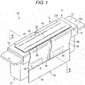
- FIG. 1 is a perspective view illustrating an ink jet head 10 according to an embodiment.
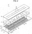
- FIG. 2 is an exploded perspective view of the ink jet head 10.
- FIG. 3 is a sectional view taken along line III-III in FIG. 1 .
- FIG. 4 is a perspective view illustrating a configuration of the ink jet head.
- the ink jet head 10 is a so-called side shooter type ink jet head.
- the ink jet head 10 is mounted in an ink jet printer, and is connected to an ink tank through a component such as a tube.
- the ink jet head 10 includes a head main body 11, a unit portion 12, and a pair of circuit substrates 13.
- the head main body 11 forms a device for discharging ink.
- the head main body 11 is attached to the unit portion 12.
- the unit portion 12 includes a manifold that forms a portion of a path between the head main body 11 and an ink tank, and a member for attaching the ink jet head 10 to an inner portion of the ink jet printer.
- the pair of circuit substrates 13 are attached to the head main body 11.
- the head main body 11 includes a base plate 15, a nozzle plate 16, a frame member 17, and a pair of drive elements 18 (only one drive element is illustrated in FIG. 3 ) which comprises a piezoelectric member.
- the base plate 15 is an example of a base member.
- An ink chamber 19 to which ink is supplied is formed inside the head main body 11.
- the base plate 15 is formed of a ceramic such as alumina, in a rectangular plate shape.
- the base plate 15 includes a planar mounting surface 21.
- a plurality of supply holes 22 and a plurality of discharge holes 23 extend through the base plate 15 and open through the mounting surface 21.
- a row of spaced apart supply holes 22 are provided in parallel with each other in a longitudinal direction of the base plate 15 at a center portion of the base plate 15 as illustrated in Fig. 2 .
- the supply hole 22 communicates with an ink supply portion 12a of the manifold of the unit portion 12.
- the supply hole 22 is fluidly connected to the ink tank through the ink supply portion 12a. Ink of the ink tank is supplied from the supply hole 22 to the ink chamber 19.
- the discharge holes 23 are provided in parallel with each other in two rows with the row of supply holes 22 extending therebetween. As illustrated in FIG. 3 , the discharge hole 23 communicates with an ink discharge portion 12b of the manifold of the unit portion 12. The discharge hole 23 is connected to the ink tank through the ink discharge portion 12b. The ink of the ink chamber 19 may be recovered from the discharge hole 23 and flows to the ink tank. In this manner, the ink is circulated between the ink tank and the ink chamber 19.
- the nozzle plate 16 is formed by a rectangular-shaped film made of polyimide of which, for example, provides an oil repellent function on the surface of the nozzle plate.
- One side surface of the nozzle plate 16 faces the mounting surface 21 of the base plate 15.
- a plurality of nozzles 25 are provided through the nozzle plate 16. The plurality of nozzles 25 are arranged in two rows parallel with each other along the longitudinal direction of the nozzle plate 16 as illustrated in Fig. 2 .
- the frame member 17 is formed in a rectangular frame shape from a nickel alloy material.
- the frame member 17 is interposed between the mounting surface 21 of the base plate 15 and the one side surface of the nozzle plate 16.
- the frame member 17 is bonded to the mounting surface 21 and to the nozzle plate 16. That is, the nozzle plate 16 is attached to the base plate 15 through the frame member 17.
- the ink chamber 19 is bounded by the base plate 15, the nozzle plate 16, and the frame member 17.
- the drive element 18 includes two piezoelectric members having a plate shape formed of, for example, lead zirconate titanate (PZT).
- PZT lead zirconate titanate
- the two piezoelectric members are bonded together with their polarization directions opposite to each other in the thickness direction thereof (i.e., opposed in the direction between the nozzle plate 16 and the base plate 15.
- the pair of drive elements 18 are bonded to the mounting surface 21 of the base plate 15.
- the pair of drive elements 18 are arranged in parallel in the ink chamber 19 with one of each of the rows of nozzles 25 located thereover.
- the drive element 18 has formed in a trapezoidal shape in profile.
- the top portion of the drive elements 18 are bonded to the nozzle plate 16.
- a plurality of grooves 27 extend inwardly of the drive elements 18 from the nozzle plate 16 side thereof.
- the grooves 27 extend in the direction intersecting the longitudinal direction of the drive element 18, and are arranged in parallel with each other in the longitudinal direction of the drive element 18 as illustrated in Fig. 4 .
- a plurality of driven pressure chambers 51 each of which provide ones of a driven flow path for discharging the ink to the groove 27 and empty dummy flow paths 52 for not discharging the ink are alternately arranged, as illustrated in FIG. 4 .
- the grooves 27 forming the dummy flow paths 52 are sealed resin at both ends of the groove 27 by a sealing portion 53 formed of a sealing resin. As illustrated in FIG. 6 , the sealing portion 53 extends between the mounting surface 21 of the base plate 15 and the nozzle plate 16. With this, flowing of the ink in the ink chamber 19 into the dummy flow path 52 is prevented, and ink is not present therein.
- the nozzles 25 of the nozzle plates 16 are positioned to open into the driven pressure chambers 51 formed in part by the grooves 27.
- An electrode 28 is provided in each of the plurality of grooves 27.
- the electrodes 28 are formed by etching a nickel thin film through a patterned photoresist.
- the electrode 28 covers the inner side surfaces of the grooves 27.
- a plurality of wiring patterns 35 extend over the base of the long groves 27 of the drive element 18 from the mounting surface 21 of the base plate 15.
- these wiring patterns 35 are formed by etching a nickel thin film through a patterned photoresist.
- the wiring patterns 35 extend from one side end portion 21a and the other, opposed, side end portion 21b of the mounting surface 21, respectively.
- the side end portions 21a and 21b include not only the opposed edges of the mounting surface 21, but also the periphery region inward of the edges thereof. Therefore, the wiring pattern 35 may also extend from a location inwardly of the sides of the mounting surface 21.
- the wiring pattern 35 extending from the one side end portion 21a will be described as representative.
- the basic configuration of the wiring pattern 35 extending from the other side end portion 21b is the same as that of the wiring pattern 35 of the one side end portion 21a.
- the wiring pattern 35 includes first portions 35a and second portions 35b. As illustrated in FIG. 2 , the first portions 35a of the wiring pattern 35 extend from the side end portion 21a of the mounting surface 21 toward the drive element 18 in straight line paths. The first portions 35a extend in parallel with each other. The second portions 35b of the wiring pattern 35 extend from an end portion of the first portions 35a groove to the electrodes 28. The second portions 35b are electrically connected to the electrodes 28, respectively.
- the wiring patterns 35 according to the embodiment include first wiring patterns 35p connected to the electrode 28 of the dummy flow path 52 and second wiring patterns 35m connected to the electrodes 28 of the driven pressure chambers 51. As illustrated in FIG. 4 , the second wiring pattern 35m connected to the electrodes 28 of the driven pressure chamber 51 is always connected to ground (GND).
- the electrode 28 of the dummy flow path 52 is divided into two portions, and one portion is formed as a common electrode.
- the other portion of the electrode 28 of the dummy flow path 52 is operated as an individual electrode to which positive charge is applied. Accordingly, the first wiring pattern 35p is connected to the other portion of the electrode 28 that is operated as the individual electrode of the dummy flow path 52.
- a first protective layer 54 formed of an inorganic insulating material is formed on a surface on a wiring pattern 35 side of the mounting surface 21 of the base plate 15.
- the first protective layer 54 is formed by, for example, spin coating.
- the first protective layer 54 forms a planarization stop layer 55 used during planarizing the surface of the wiring pattern 35.
- a second protective layer 56 formed of an electric insulating material having good electric insulation characteristics is stacked on the planarization layer 55 formed of the wiring pattern 35 and the first protective layer 54.
- the second protective layer 56 is formed of, for example, a parylene film formed of an organic insulating material.
- the parylene film of the second protective layer 56 is formed by vapor deposition polymerization.
- the second protective layer 56 may also include a silicon nitride film as the inorganic material layer. It is possible to use a chemical vapor deposition (CVD) method, an RF magnetron sputtering method, and an atomic layer deposition (ALD) method as a manufacturing method of the silicon nitride film layer.
- CVD chemical vapor deposition
- ALD atomic layer deposition
- each of the pair of circuit substrates 13 includes a substrate main body 44 and a pair of film carrier packages (FCP) 45.
- the FCP is also referred to as a tape carrier package (TCP).
- the substrate main body 44 is a printed wiring plate having rigidity formed in a rectangular shape.
- Various electronic components and connectors are mounted on the substrate main body 44.
- the pair of FCPs 45 is attached to the substrate main body 44.
- Each of the pair of FCPs 45 includes a flexible resin film 46 on which a plurality of wirings are formed and an IC 47 connected to the plurality of wirings.
- the film 46 is a tape automated bonding (TAB) film.
- the IC 47 is a component for applying a voltage to the electrode 28.
- the IC 47 is fixed to the film 46 by resin.
- an end portion of the FCP 45 is connected to the first portions 35a of the wiring pattern 35 by thermocompression bonding using an anisotropic conductive film (ACF) 48 as the bonding material.
- ACF anisotropic conductive film
- the FCP 45 is electrically connected to the wiring pattern 35 such that the IC 47 is electrically connected to the electrode 28 through the wiring of the FCP 45.
- the IC 47 applies a voltage to the electrode 28 through the wiring of the film 46.
- the IC 47 applies a non-zero voltage to the electrodes 28 of the adjacent dummy pressure chambers 52 which each share a common wall 18 with a selected driven pressure chamber 51, the volume of the selected driven pressure chamber 51 groove is increased or decreased as a result of shear mode deformation of the drive element 18.
- the volume of the selected driven pressure chamber 51 increases, and ink is drawn therein from the ink chamber 19.
- the volume of the selected driven pressure chamber 51 contracts and the pressure of the ink in the selected driven pressure chamber 51 groove is increased such that the ink is discharged from the nozzle 25, i.e., the ink is squeezed out of the selected driven pressure chamber 51 at least in part through the nozzle associated therewith.
- the electrodes 28 of the dummy pressure chambers on the drive elements 18 which form common walls with the selected driven pressure chamber need be biased to cause a change in the volume of the selected driven pressure chamber 51.
- the plurality of driven pressure chambers 51 that serve as the drive flow path for discharging the ink to the groove 27 and the empty dummy flow paths 52 which do not discharge ink are alternatively arranged in the drive element 18. Therefore, when ink is discharged through a nozzle 25 by individually driving and independently operating the driven pressure chambers 51, movement of the walls of a driven pressure chamber 51 in which the shear mode deformation is performed is not transmitted to an adjacent driven pressure chamber 51, because of the presence of an intervening dummy flow path 52 therebetween. As a result, it is possible to quickly perform an operation to only drive an individual driven pressure chamber 51 of the ink jet head 10, and it is possible to achieve high precision, high speed printing.
- the dummy flow path 52 is sealed by the sealing portion 53 formed of sealing resin at both ends of the groove 27 such that flowing of the ink from the ink chamber 19 to the dummy flow path 52 is prevented. Accordingly, each nozzle 25 of the nozzle plate 16 is opposed to a position corresponding to a driven pressure chamber 51 of the groove 27. Therefore, for example, when a nozzle 25 of the nozzle plate 16 is formed by laser processing, the laser beam is not directed to a location overlying the dummy flow paths 52.
- the nozzles 25 of the nozzle plate 16 are formed by the laser processing, since the laser beam is not directed to the locations of the nozzle plate overlying the electrode 28 of the dummy flow paths 52, the electric insulating layer of the electrode 28 of the dummy flow path 52 is not damaged.
- the first protective layer 54 formed of the inorganic insulating material is formed on a surface on the wiring pattern 35 on the mounting surface 21 of the base plate 15, and the planarization stop layer 55 for planarizing a surface of the wiring pattern 35 includes the first protective layer 54.
- the second protective layer 56 formed of an electric insulating layer having good electric insulation characteristics is stacked on the planarization layer 55 formed by the wiring pattern 35 and the first protective layer 54.
- the wiring pattern 35 according to the embodiment includes the first wiring pattern 35p connected to the electrode 28 of the dummy flow path 52 and the second wiring pattern 35m connected to the electrode 28 of the driven pressure chamber 51. Accordingly, as illustrated in FIG. 4 , the second wiring pattern 35m connected to the electrode 28 of the driven pressure chamber 51 is always connected to GND. Therefore, even when liquid ink having electric conductivity or liquid having polarity flows to an inside of the driven pressure chamber 51, it is possible to prevent the electrode 28 of the driven pressure chamber 51 from being short-circuited. In addition, if the electrode protective film is formed on the electrode 28 of the ink jet head 10 of the structure, even if there is a pinhole on the electrode protective film, it is possible to maintain insulating properties between the electrode 28 and the ink.
- the ink jet head which can maintain the insulating properties between the electrode and the ink.
Landscapes
- Engineering & Computer Science (AREA)
- Manufacturing & Machinery (AREA)
- Particle Formation And Scattering Control In Inkjet Printers (AREA)
Abstract
Description
- The present invention generally relates to the field of ink jet printing technology and, in particular, to ink jet head structures.
- In the related art, a so-called shear mode type ink jet head that discharges ink droplets from a nozzle using shear mode deformation of a piezoelectric member is known. As an example of a shear mode type ink jet head structure, there is a structure in which a piezoelectric ceramic plate, an ink chamber plate, and a nozzle plate are stacked. A plurality of grooves, and side walls between the grooves, are formed in the piezoelectric ceramic plate, and electrodes are formed on the side walls of an inner surface of the grooves. The ink chamber plate covers the grooves of the piezoelectric ceramic plate to form ink chambers.
- In the shear mode type ink jet head structure, since ink and the electrode may be in contact with each other, if liquid having electric conductivity or liquid having polarity (an electric di-pole) is to be used as the ink, an electrode protective film is first formed on the electrode. For example, an inorganic insulating film formed of an inorganic material and an organic insulating film formed of an organic material are sequentially formed on the groove inner surface so as to cover the electrode, and thus the protective layer includes two film layers comprising the inorganic insulating film and the organic insulating film. Accordingly, when manufacturing the head, after bonding a piezoelectric ceramic plate on which an electrode is formed to the ink chamber plate, the protective layer includes the two film layers comprising the inorganic insulating film and the organic insulating film, and the nozzle plate is bonded to an end surface of a bonding body thereof.
- To further improve such an ink jet head structure, there is provided an ink jet head comprising:
- a base member comprising a mounting surface;
- a plurality of walls attached to the mounting surface of the base member, each of the walls including a first piezoelectric layer having a first polarization direction and a second piezoelectric layer having a second polarization direction opposite to the first polarization direction, and defining a plurality of flow paths between the walls, the flow paths including first and second flow paths alternating with one another;
- a nozzle plate comprising a plurality of openings, each of which communicates with one of the first flow paths;
- an ink supply unit fluidly coupled to the first flow paths;
- electrodes on side surfaces of the walls;
- first and second wirings, each extending along the mounting surface of the base member and each being individually connected to one of the electrodes; and
- a plurality of first protective layers on the mounting surface of the base member, the first wiring extending between a first pair of the first protective layers and the second wiring extending between a second pair of the first protective layers; and
- a second protective layer comprising an electrically insulating layer covering the first protective layers and the first and second wirings.
- Preferably, the second flow paths are blocked.
- Preferably still, the 3 ink jet head further comprises:
- a sealing portion at opposed ends of each second flow path to prevent the ink from flowing thereinto.
- Preferably yet, the electrodes include first electrodes at the side surfaces of the walls that define the first flow paths and second electrodes at the side surfaces of the walls that define the second flow paths.
- Suitably, the first electrodes of each of the first flow paths are electrically connected together, and the second electrodes of each of the second flow paths are electrically isolated from each other.
- In the above ink jet head, a fixed voltage is preferably applied to the first electrodes when ink is being ejected through the openings.
- Also in the above ink jet head, the fixed voltage is preferably ground voltage.
- Further in the above ink jet head, a variable voltage is preferably applied to the second electrodes when ink is being ejected through the openings.
- The invention also relates to an ink jet head, comprising:
- a base;
- an ink reservoir;
- a first chamber on the base and fluidly connected to the ink reservoir;
- a second chamber on the base disposed adjacent a first side of the first chamber and sharing a first common wall with the first chamber;
- a third chamber on the base disposed adjacent a second side of the first chamber different from the first side and sharing a second common wall with the first chamber;
- a first electrode in the first chamber and in contact with side surfaces of the first and second common walls;
- a second electrode in the second chamber and in contact with a side surface of the first common wall; and
- a third electrode in the third chamber and in contact with a side surface of the second common wall, wherein
- first, second, and third wirings each electrically connected to the first, second, and third electrodes, respectively, and
- each of the wirings extend from the respective first, second, or third chamber along the base and having opposed sides, a first insulating layer disposed adjacent to the wiring and abutting opposed sides of the wiring, and a second insulating layer disposed over and contacting the wiring and the first insulating layer.
- Preferably, during operation, a fixed voltage is applied to the first electrode, and a variable voltage is applied to the second and third electrodes.
- In the above ink jet head, the fixed voltage is preferably ground voltage.
- Preferably still, the variable voltage includes a voltage greater than ground voltage and less than ground voltage.
- Preferably yet, the ink jet head further comprises:
- a cover plate that covers the first, second and third chambers, and an opening extends through the cover plate to expose the first chamber.
- Conveniently, the first and second common walls each include a first piezoelectric layer and a second piezoelectric layer.
- In the above ink jet head, the first piezoelectric layer has preferably a first polarization direction and the second piezoelectric layer has preferably a second polarization direction opposite the first polarization direction.
- The invention further concerns an ink jet head comprising:
- a base;
- a plurality of walls attached to a surface of the base, each of the walls including a first piezoelectric layer having a first polarization direction and a second piezoelectric layer having a second polarization direction opposite to the first polarization direction, and defining a plurality of chambers between the walls, the chambers including driven pressure chambers and dummy pressure chambers alternating with one another;
- a nozzle plate comprising a plurality of openings, each of which communicates with one of the driven pressure chambers;
- an ink supply unit fluidly coupled to the driven pressure chambers;
- electrodes on side surfaces of the walls; and
- a plurality of wirings each connected to one of the electrodes and extending from one of the chambers, wherein
- a first insulating layer is disposed adjacent to each wiring and abut opposed sides of the wiring, and a second insulating layer disposed over and contacting the wiring and the first insulating layer.
- Preferably, during operation, a ground voltage is applied to the first electrode, and a variable voltage is applied to the second and third electrodes.
- Preferably still, the variable voltage includes a voltage greater than ground voltage and less than ground voltage.
Preferably yet, the electrodes include first electrodes at the side surfaces of the walls that define the driven pressure chambers and second electrodes at the side surfaces of the walls that define the dummy pressure chambers. - Suitably, the first electrodes of each of the driven pressure chambers are electrically connected together, and the second electrodes of each of the dummy pressure chambers are electrically isolated from each other.
- The above and other objects, features and advantages of the present invention will be made apparent from the following description of the preferred embodiments, given as non-limiting examples, with reference to the accompanying drawings, in which:
-
FIG. 1 is a perspective view illustrating a schematic configuration of an ink jet head of a first embodiment. -
FIG. 2 is an exploded perspective view of the ink jet head. -
FIG. 3 is a sectional view taken along line III-III inFIG. 1 . -
FIG. 4 is a perspective view illustrating a main configuration of the ink jet head. -
FIG. 5 is a vertical cross-sectional view of a main part illustrating a discharge state of ink of the ink jet head. -
FIG. 6 is a vertical cross-sectional view of a main part illustrating a dummy flow path of the ink jet head. -
FIG. 7 is a vertical cross-sectional view of a main part illustrating a protective layer of a wiring pattern of the ink jet head. - In the ink jet head structure of the related art, there is a problem that contact between an electrode and the ink cannot be prevented when there is a pinhole in the protective film formed of an organic material.
- In general, according to an embodiment, an ink jet head includes a base, walls attached to the base and defining flow paths between the walls, the flow paths including first and second flow paths alternating with one another, a nozzle plate comprising openings, each of which communicates with one of the first flow paths, an ink supply unit fluidly coupled to the first flow paths, electrodes on side surfaces of the walls, first and second wirings, each extending along the base and each being individually connected to one of the electrodes, a plurality of first protective layers on the base, the first wiring extending between a first pair of the first protective layers and the second wiring extending between a second pair of the first protective layers, and a second protective layer comprising an electrically insulating layer covering the first protective layers and the first and second wirings.
- Hereinafter, an embodiment will be described with reference to
FIG. 1 to FIG. 7 .FIG. 1 is a perspective view illustrating anink jet head 10 according to an embodiment.FIG. 2 is an exploded perspective view of theink jet head 10.FIG. 3 is a sectional view taken along line III-III inFIG. 1 .FIG. 4 is a perspective view illustrating a configuration of the ink jet head. - As illustrated in
FIG. 1 , theink jet head 10 is a so-called side shooter type ink jet head. Theink jet head 10 is mounted in an ink jet printer, and is connected to an ink tank through a component such as a tube. Theink jet head 10 includes a headmain body 11, aunit portion 12, and a pair ofcircuit substrates 13. - The head
main body 11 forms a device for discharging ink. The headmain body 11 is attached to theunit portion 12. Theunit portion 12 includes a manifold that forms a portion of a path between the headmain body 11 and an ink tank, and a member for attaching theink jet head 10 to an inner portion of the ink jet printer. The pair ofcircuit substrates 13 are attached to the headmain body 11. - As illustrated in
FIG. 3 , the headmain body 11 includes abase plate 15, anozzle plate 16, aframe member 17, and a pair of drive elements 18 (only one drive element is illustrated inFIG. 3 ) which comprises a piezoelectric member. Thebase plate 15 is an example of a base member. Anink chamber 19 to which ink is supplied is formed inside the headmain body 11. - As illustrated in
FIG. 2 , for example, thebase plate 15 is formed of a ceramic such as alumina, in a rectangular plate shape. Thebase plate 15 includes a planar mountingsurface 21. A plurality of supply holes 22 and a plurality of discharge holes 23 extend through thebase plate 15 and open through the mountingsurface 21. - A row of spaced apart supply
holes 22 are provided in parallel with each other in a longitudinal direction of thebase plate 15 at a center portion of thebase plate 15 as illustrated inFig. 2 . As illustrated inFIG. 3 , thesupply hole 22 communicates with anink supply portion 12a of the manifold of theunit portion 12. Thesupply hole 22 is fluidly connected to the ink tank through theink supply portion 12a. Ink of the ink tank is supplied from thesupply hole 22 to theink chamber 19. - As illustrated in
FIG. 2 , the discharge holes 23 are provided in parallel with each other in two rows with the row of supply holes 22 extending therebetween. As illustrated inFIG. 3 , thedischarge hole 23 communicates with anink discharge portion 12b of the manifold of theunit portion 12. Thedischarge hole 23 is connected to the ink tank through theink discharge portion 12b. The ink of theink chamber 19 may be recovered from thedischarge hole 23 and flows to the ink tank. In this manner, the ink is circulated between the ink tank and theink chamber 19. - As illustrated in
FIG. 2 , thenozzle plate 16 is formed by a rectangular-shaped film made of polyimide of which, for example, provides an oil repellent function on the surface of the nozzle plate. One side surface of thenozzle plate 16 faces the mountingsurface 21 of thebase plate 15. A plurality ofnozzles 25 are provided through thenozzle plate 16. The plurality ofnozzles 25 are arranged in two rows parallel with each other along the longitudinal direction of thenozzle plate 16 as illustrated inFig. 2 . - The
frame member 17 is formed in a rectangular frame shape from a nickel alloy material. Theframe member 17 is interposed between the mountingsurface 21 of thebase plate 15 and the one side surface of thenozzle plate 16. Theframe member 17 is bonded to the mountingsurface 21 and to thenozzle plate 16. That is, thenozzle plate 16 is attached to thebase plate 15 through theframe member 17. Theink chamber 19 is bounded by thebase plate 15, thenozzle plate 16, and theframe member 17. - The
drive element 18 includes two piezoelectric members having a plate shape formed of, for example, lead zirconate titanate (PZT). The two piezoelectric members are bonded together with their polarization directions opposite to each other in the thickness direction thereof (i.e., opposed in the direction between thenozzle plate 16 and thebase plate 15. - The pair of
drive elements 18 are bonded to the mountingsurface 21 of thebase plate 15. The pair ofdrive elements 18 are arranged in parallel in theink chamber 19 with one of each of the rows ofnozzles 25 located thereover. As illustrated inFIG. 2 , thedrive element 18 has formed in a trapezoidal shape in profile. The top portion of thedrive elements 18 are bonded to thenozzle plate 16. - A plurality of
grooves 27 extend inwardly of thedrive elements 18 from thenozzle plate 16 side thereof. Thegrooves 27 extend in the direction intersecting the longitudinal direction of thedrive element 18, and are arranged in parallel with each other in the longitudinal direction of thedrive element 18 as illustrated inFig. 4 . As illustrated inFigs. 4 and 5 , in each of thedrive elements 18 according to the embodiment, a plurality of drivenpressure chambers 51, each of which provide ones of a driven flow path for discharging the ink to thegroove 27 and emptydummy flow paths 52 for not discharging the ink are alternately arranged, as illustrated inFIG. 4 . - The
grooves 27 forming thedummy flow paths 52 are sealed resin at both ends of thegroove 27 by a sealingportion 53 formed of a sealing resin. As illustrated inFIG. 6 , the sealingportion 53 extends between the mountingsurface 21 of thebase plate 15 and thenozzle plate 16. With this, flowing of the ink in theink chamber 19 into thedummy flow path 52 is prevented, and ink is not present therein. Thenozzles 25 of thenozzle plates 16 are positioned to open into the drivenpressure chambers 51 formed in part by thegrooves 27. - An
electrode 28 is provided in each of the plurality ofgrooves 27. For example, theelectrodes 28 are formed by etching a nickel thin film through a patterned photoresist. Theelectrode 28 covers the inner side surfaces of thegrooves 27. - As illustrated in
FIG. 2 , a plurality ofwiring patterns 35 extend over the base of thelong groves 27 of thedrive element 18 from the mountingsurface 21 of thebase plate 15. For example, thesewiring patterns 35 are formed by etching a nickel thin film through a patterned photoresist. - The
wiring patterns 35 extend from oneside end portion 21a and the other, opposed,side end portion 21b of the mountingsurface 21, respectively. Theside end portions surface 21, but also the periphery region inward of the edges thereof. Therefore, thewiring pattern 35 may also extend from a location inwardly of the sides of the mountingsurface 21. - Hereinafter, the
wiring pattern 35 extending from the oneside end portion 21a will be described as representative. The basic configuration of thewiring pattern 35 extending from the otherside end portion 21b is the same as that of thewiring pattern 35 of the oneside end portion 21a. - The
wiring pattern 35 includesfirst portions 35a andsecond portions 35b. As illustrated inFIG. 2 , thefirst portions 35a of thewiring pattern 35 extend from theside end portion 21a of the mountingsurface 21 toward thedrive element 18 in straight line paths. Thefirst portions 35a extend in parallel with each other. Thesecond portions 35b of thewiring pattern 35 extend from an end portion of thefirst portions 35a groove to theelectrodes 28. Thesecond portions 35b are electrically connected to theelectrodes 28, respectively. - In addition, the
wiring patterns 35 according to the embodiment includefirst wiring patterns 35p connected to theelectrode 28 of thedummy flow path 52 andsecond wiring patterns 35m connected to theelectrodes 28 of the drivenpressure chambers 51. As illustrated inFIG. 4 , thesecond wiring pattern 35m connected to theelectrodes 28 of the drivenpressure chamber 51 is always connected to ground (GND). - The
electrode 28 of thedummy flow path 52 is divided into two portions, and one portion is formed as a common electrode. The other portion of theelectrode 28 of thedummy flow path 52 is operated as an individual electrode to which positive charge is applied. Accordingly, thefirst wiring pattern 35p is connected to the other portion of theelectrode 28 that is operated as the individual electrode of thedummy flow path 52. - In the embodiment, as illustrated in
FIG. 7 , for example, a firstprotective layer 54 formed of an inorganic insulating material is formed on a surface on awiring pattern 35 side of the mountingsurface 21 of thebase plate 15. The firstprotective layer 54 is formed by, for example, spin coating. The firstprotective layer 54 forms aplanarization stop layer 55 used during planarizing the surface of thewiring pattern 35. - Furthermore, a second
protective layer 56 formed of an electric insulating material having good electric insulation characteristics is stacked on theplanarization layer 55 formed of thewiring pattern 35 and the firstprotective layer 54. The secondprotective layer 56 is formed of, for example, a parylene film formed of an organic insulating material. The parylene film of the secondprotective layer 56 is formed by vapor deposition polymerization. In addition, the secondprotective layer 56 may also include a silicon nitride film as the inorganic material layer. It is possible to use a chemical vapor deposition (CVD) method, an RF magnetron sputtering method, and an atomic layer deposition (ALD) method as a manufacturing method of the silicon nitride film layer. - As illustrated in
FIG. 1 , each of the pair ofcircuit substrates 13 includes a substratemain body 44 and a pair of film carrier packages (FCP) 45. The FCP is also referred to as a tape carrier package (TCP). - The substrate
main body 44 is a printed wiring plate having rigidity formed in a rectangular shape. Various electronic components and connectors are mounted on the substratemain body 44. In addition, the pair of FCPs 45 is attached to the substratemain body 44. - Each of the pair of FCPs 45 includes a
flexible resin film 46 on which a plurality of wirings are formed and anIC 47 connected to the plurality of wirings. Thefilm 46 is a tape automated bonding (TAB) film. TheIC 47 is a component for applying a voltage to theelectrode 28. TheIC 47 is fixed to thefilm 46 by resin. - As illustrated in
FIG. 3 , an end portion of theFCP 45 is connected to thefirst portions 35a of thewiring pattern 35 by thermocompression bonding using an anisotropic conductive film (ACF) 48 as the bonding material. As a result, the plurality of wirings of theFCP 45 are electrically connected to thewiring pattern 35. - The
FCP 45 is electrically connected to thewiring pattern 35 such that theIC 47 is electrically connected to theelectrode 28 through the wiring of theFCP 45. TheIC 47 applies a voltage to theelectrode 28 through the wiring of thefilm 46. - When the
IC 47 applies a non-zero voltage to theelectrodes 28 of the adjacentdummy pressure chambers 52 which each share acommon wall 18 with a selected drivenpressure chamber 51, the volume of the selected drivenpressure chamber 51 groove is increased or decreased as a result of shear mode deformation of thedrive element 18. As a result, when a positive potential is applied to theelectrodes 28 of the dummy pressure chambers on thedrive elements 18 which form common walls with the selected driven pressure chamber, the volume of the selected drivenpressure chamber 51 increases, and ink is drawn therein from theink chamber 19. When the voltage on these same electrodes is reversed, i.e., a negative potential is applied thereto, the volume of the selected drivenpressure chamber 51 contracts and the pressure of the ink in the selected drivenpressure chamber 51 groove is increased such that the ink is discharged from thenozzle 25, i.e., the ink is squeezed out of the selected drivenpressure chamber 51 at least in part through the nozzle associated therewith. Note, one, or both of theelectrodes 28 of the dummy pressure chambers on thedrive elements 18 which form common walls with the selected driven pressure chamber need be biased to cause a change in the volume of the selected drivenpressure chamber 51. - According to a configuration of the
ink jet head 10 according to the embodiment, as illustrated inFIG. 4 , the plurality of drivenpressure chambers 51 that serve as the drive flow path for discharging the ink to thegroove 27 and the emptydummy flow paths 52 which do not discharge ink are alternatively arranged in thedrive element 18. Therefore, when ink is discharged through anozzle 25 by individually driving and independently operating the drivenpressure chambers 51, movement of the walls of a drivenpressure chamber 51 in which the shear mode deformation is performed is not transmitted to an adjacent drivenpressure chamber 51, because of the presence of an interveningdummy flow path 52 therebetween. As a result, it is possible to quickly perform an operation to only drive an individual drivenpressure chamber 51 of theink jet head 10, and it is possible to achieve high precision, high speed printing. - The
dummy flow path 52 is sealed by the sealingportion 53 formed of sealing resin at both ends of thegroove 27 such that flowing of the ink from theink chamber 19 to thedummy flow path 52 is prevented. Accordingly, eachnozzle 25 of thenozzle plate 16 is opposed to a position corresponding to a drivenpressure chamber 51 of thegroove 27. Therefore, for example, when anozzle 25 of thenozzle plate 16 is formed by laser processing, the laser beam is not directed to a location overlying thedummy flow paths 52. Accordingly, when thenozzles 25 of thenozzle plate 16 are formed by the laser processing, since the laser beam is not directed to the locations of the nozzle plate overlying theelectrode 28 of thedummy flow paths 52, the electric insulating layer of theelectrode 28 of thedummy flow path 52 is not damaged. - In addition, for example, in the embodiment, the first
protective layer 54 formed of the inorganic insulating material is formed on a surface on thewiring pattern 35 on the mountingsurface 21 of thebase plate 15, and theplanarization stop layer 55 for planarizing a surface of thewiring pattern 35 includes the firstprotective layer 54. Furthermore, the secondprotective layer 56 formed of an electric insulating layer having good electric insulation characteristics is stacked on theplanarization layer 55 formed by thewiring pattern 35 and the firstprotective layer 54. With this structure, theplanarization stop layer 55 having planarization characteristics of thewiring pattern 35 and the secondprotective layer 56 having good ink resistance characteristics and coverage properties are sequentially formed. Therefore, even a when liquid having electric conductivity or liquid having polarity (a di-pole)is used as the ink, it is possible to ensure insulating properties with good reproducibility between the ink and theelectrode 28 when the ink is supplied to theink chamber 19 inside the headmain body 11. - Furthermore, the
wiring pattern 35 according to the embodiment includes thefirst wiring pattern 35p connected to theelectrode 28 of thedummy flow path 52 and thesecond wiring pattern 35m connected to theelectrode 28 of the drivenpressure chamber 51. Accordingly, as illustrated inFIG. 4 , thesecond wiring pattern 35m connected to theelectrode 28 of the drivenpressure chamber 51 is always connected to GND. Therefore, even when liquid ink having electric conductivity or liquid having polarity flows to an inside of the drivenpressure chamber 51, it is possible to prevent theelectrode 28 of the drivenpressure chamber 51 from being short-circuited. In addition, if the electrode protective film is formed on theelectrode 28 of theink jet head 10 of the structure, even if there is a pinhole on the electrode protective film, it is possible to maintain insulating properties between theelectrode 28 and the ink. - According to the embodiment, even when the liquid having electric conductivity or the liquid having polarity is used as the ink, it is possible to provide an ink jet head which can maintain the insulating properties between the electrode and the ink.
- While certain embodiments have been described, these embodiments have been presented by way of example only, and are not intended to limit the scope of the inventions. Indeed, the novel embodiments described herein may be embodied in a variety of other forms; furthermore, various omissions, substitutions and changes in the form of the embodiments described herein may be made without departing from the framework of the inventions. The accompanying claims and their equivalents are intended to cover such forms or modifications as would fall within the scope and framework of the inventions.
Claims (15)
- An ink jet head comprising:a base member comprising a mounting surface;a plurality of walls attached to the mounting surface of the base member, each of the walls including a first piezoelectric layer having a first polarization direction and a second piezoelectric layer having a second polarization direction opposite to the first polarization direction, and defining a plurality of flow paths between the walls, the flow paths including first and second flow paths alternating with one another;a nozzle plate comprising a plurality of openings, each of which communicates with one of the first flow paths;an ink supply unit fluidly coupled to the first flow paths;electrodes on side surfaces of the walls;first and second wirings, each extending along the mounting surface of the base member and each being individually connected to one of the electrodes; anda plurality of first protective layers on the mounting surface of the base member, the first wiring extending between a first pair of the first protective layers and the second wiring extending between a second pair of the first protective layers; anda second protective layer comprising an electrically insulating layer covering the first protective layers and the first and second wirings.
- The ink jet head according to claim 1, wherein the second flow paths are blocked.
- The ink jet head according to claim 1 or 2, further comprising:a sealing portion at opposed ends of each second flow path to prevent the ink from flowing thereinto.
- The ink jet head according to any one of claims 1 to 3, wherein the electrodes include first electrodes at the side surfaces of the walls that define the first flow paths and second electrodes at the side surfaces of the walls that define the second flow paths.
- The ink jet head according to claim 4, wherein the first electrodes of each of the first flow paths are electrically connected together, and the second electrodes of each of the second flow paths are electrically isolated from each other.
- An ink jet head, comprising:a base;an ink reservoir;a first chamber on the base and fluidly connected to the ink reservoir;a second chamber on the base disposed adjacent a first side of the first chamber and sharing a first common wall with the first chamber;a third chamber on the base disposed adjacent a second side of the first chamber different from the first side and sharing a second common wall with the first chamber;a first electrode in the first chamber and in contact with side surfaces of the first and second common walls;a second electrode in the second chamber and in contact with a side surface of the first common wall; anda third electrode in the third chamber and in contact with a side surface of the second common wall, whereinfirst, second, and third wirings each electrically connected to the first, second, and third electrodes, respectively, andeach of the wirings extend from the respective first, second, or third chamber along the base and having opposed sides, a first insulating layer disposed adjacent to the wiring and abutting opposed sides of the wiring, and a second insulating layer disposed over and contacting the wiring and the first insulating layer.
- The ink jet head according to claim 6, wherein during operation, a fixed voltage is applied to the first electrode, and a variable voltage is applied to the second and third electrodes.
- The ink jet head according to claim 7, wherein the variable voltage includes a voltage greater than ground voltage and less than ground voltage.
- The ink jet head according to any one of claims 6 to 8, further comprising:a cover plate that covers the first, second and third chambers, and an opening extends through the cover plate to expose the first chamber.
- The ink jet head according to any one of claims 6 to 9, wherein the first and second common walls each include a first piezoelectric layer and a second piezoelectric layer.
- An ink jet head comprising:a base;a plurality of walls attached to a surface of the base, each of the walls including a first piezoelectric layer having a first polarization direction and a second piezoelectric layer having a second polarization direction opposite to the first polarization direction, and defining a plurality of chambers between the walls, the chambers including driven pressure chambers and dummy pressure chambers alternating with one another;a nozzle plate comprising a plurality of openings, each of which communicates with one of the driven pressure chambers;an ink supply unit fluidly coupled to the driven pressure chambers;electrodes on side surfaces of the walls; anda plurality of wirings each connected to one of the electrodes and extending from one of the chambers, whereina first insulating layer is disposed adjacent to each wiring and abut opposed sides of the wiring, and a second insulating layer disposed over and contacting the wiring and the first insulating layer.
- The ink jet head according to claim 11, wherein during operation, a ground voltage is applied to the first electrode, and a variable voltage is applied to the second and third electrodes.
- The ink jet head according to claim 11 or 12, wherein the variable voltage includes a voltage greater than ground voltage and less than ground voltage.
- The ink jet head according to any one of claims 11 to 13, wherein the electrodes include first electrodes at the side surfaces of the walls that define the driven pressure chambers and second electrodes at the side surfaces of the walls that define the dummy pressure chambers.
- The ink jet head according to claim 14, wherein the first electrodes of each of the driven pressure chambers are electrically connected together, and the second electrodes of each of the dummy pressure chambers are electrically isolated from each other.
Applications Claiming Priority (1)
| Application Number | Priority Date | Filing Date | Title |
|---|---|---|---|
| JP2016017983A JP2017136724A (en) | 2016-02-02 | 2016-02-02 | Inkjet head |
Publications (3)
| Publication Number | Publication Date |
|---|---|
| EP3210780A2 true EP3210780A2 (en) | 2017-08-30 |
| EP3210780A3 EP3210780A3 (en) | 2017-09-13 |
| EP3210780B1 EP3210780B1 (en) | 2018-10-17 |
Family
ID=57851005
Family Applications (1)
| Application Number | Title | Priority Date | Filing Date |
|---|---|---|---|
| EP17152261.8A Not-in-force EP3210780B1 (en) | 2016-02-02 | 2017-01-19 | Ink jet head |
Country Status (4)
| Country | Link |
|---|---|
| US (1) | US20170217178A1 (en) |
| EP (1) | EP3210780B1 (en) |
| JP (1) | JP2017136724A (en) |
| CN (2) | CN107020815B (en) |
Families Citing this family (7)
| Publication number | Priority date | Publication date | Assignee | Title |
|---|---|---|---|---|
| JP2017136724A (en) * | 2016-02-02 | 2017-08-10 | 東芝テック株式会社 | Inkjet head |
| JP2019051636A (en) * | 2017-09-14 | 2019-04-04 | 東芝テック株式会社 | Inkjet head and inkjet printer |
| JP6995540B2 (en) * | 2017-09-14 | 2022-02-04 | 東芝テック株式会社 | Inkjet heads and inkjet printers |
| JP6991806B2 (en) * | 2017-09-14 | 2022-01-13 | 東芝テック株式会社 | Inkjet heads and inkjet printers |
| JP7041547B2 (en) * | 2018-02-20 | 2022-03-24 | 東芝テック株式会社 | Inkjet head, inkjet printer, manufacturing method of inkjet head |
| JP6991639B2 (en) * | 2018-02-20 | 2022-01-12 | 東芝テック株式会社 | Inkjet head, inkjet printer |
| US11654683B2 (en) | 2020-11-20 | 2023-05-23 | Sii Printek Inc | Head chip, liquid jet head, liquid jet recording device, and method of manufacturing head chip |
Family Cites Families (31)
| Publication number | Priority date | Publication date | Assignee | Title |
|---|---|---|---|---|
| JPH09109392A (en) * | 1995-10-13 | 1997-04-28 | Canon Inc | Inkjet recording head manufacturing method, inkjet recording head manufactured by the same method, and inkjet recording apparatus |
| JP3305211B2 (en) * | 1996-09-10 | 2002-07-22 | 松下電器産業株式会社 | Semiconductor device and manufacturing method thereof |
| JP4472064B2 (en) * | 1998-08-31 | 2010-06-02 | 株式会社半導体エネルギー研究所 | Manufacturing method of semiconductor device |
| JP2002160364A (en) * | 2000-11-27 | 2002-06-04 | Seiko Instruments Inc | Inkjet head |
| JP2003138180A (en) * | 2001-11-06 | 2003-05-14 | Canon Inc | Ink, color filter and manufacturing method thereof, liquid crystal display and image display device |
| US7290865B2 (en) * | 2002-02-19 | 2007-11-06 | Brother Kogyo Kabushiki Kaisha | Inkjet head |
| KR20060025876A (en) * | 2004-09-17 | 2006-03-22 | 삼성전자주식회사 | Inkjet Printer Head and Manufacturing Method Thereof |
| US7470375B2 (en) * | 2004-10-22 | 2008-12-30 | Canon Kabushiki Kaisha | Method for manufacturing liquid ejection head, substrate for liquid ejection head, and liquid ejection head |
| CN100505357C (en) * | 2005-03-22 | 2009-06-24 | 精工爱普生株式会社 | Piezoelectric element, liquid ejection head and liquid ejection device |
| JP2007021925A (en) * | 2005-07-19 | 2007-02-01 | Seiko Epson Corp | Inkjet recording method |
| KR100738102B1 (en) * | 2006-02-01 | 2007-07-12 | 삼성전자주식회사 | Piezoelectric inkjet printheads |
| DE102006019505B4 (en) * | 2006-04-26 | 2008-01-03 | Infineon Technologies Ag | Process for producing a structured bottom electrode in a piezoelectric component |
| JP4848028B2 (en) * | 2009-01-21 | 2011-12-28 | 東芝テック株式会社 | Ink jet head and method of manufacturing ink jet head |
| JP2010214895A (en) * | 2009-03-18 | 2010-09-30 | Toshiba Tec Corp | Inkjet head and method for manufacturing inkjet head |
| JP2012081695A (en) * | 2010-10-14 | 2012-04-26 | Toshiba Tec Corp | Inkjet head and method of manufacturing the same |
| JP2012187864A (en) * | 2011-03-11 | 2012-10-04 | Toshiba Tec Corp | Inkjet head |
| JP5372054B2 (en) * | 2011-03-11 | 2013-12-18 | 東芝テック株式会社 | Inkjet head |
| JP2012192629A (en) * | 2011-03-16 | 2012-10-11 | Toshiba Tec Corp | Inkjet head and method of manufacturing the same |
| JP5708098B2 (en) * | 2011-03-18 | 2015-04-30 | 株式会社リコー | Liquid ejection head, liquid ejection apparatus, and image forming apparatus |
| US9028051B2 (en) * | 2011-04-05 | 2015-05-12 | Hewlett-Packard Development Company, L.P. | Shear mode physical deformation of piezoelectric mechanism |
| JP5530989B2 (en) * | 2011-08-26 | 2014-06-25 | 東芝テック株式会社 | Inkjet head |
| TWI511886B (en) * | 2011-11-18 | 2015-12-11 | Canon Kk | Liquid discharge device |
| JP2014168891A (en) * | 2013-03-04 | 2014-09-18 | Toshiba Corp | Ink jet head and production method of the same |
| JP5740422B2 (en) * | 2013-03-06 | 2015-06-24 | 株式会社東芝 | Inkjet head and inkjet recording apparatus |
| JP2015054499A (en) * | 2013-09-13 | 2015-03-23 | キヤノンファインテック株式会社 | Substrate for recording head, recording head, and recording unit |
| JP2015168177A (en) * | 2014-03-07 | 2015-09-28 | エスアイアイ・プリンテック株式会社 | Liquid ejecting head and liquid ejecting apparatus |
| JP6264654B2 (en) * | 2014-03-26 | 2018-01-24 | ブラザー工業株式会社 | Liquid ejection device and method of manufacturing liquid ejection device |
| US9421768B2 (en) * | 2014-04-02 | 2016-08-23 | Kabushiki Kaisha Toshiba | Inkjet printer head |
| JP6318793B2 (en) * | 2014-04-08 | 2018-05-09 | 株式会社リコー | Electro-mechanical transducer, electro-mechanical transducer manufacturing method, ink jet recording head, and ink jet recording apparatus |
| JP6266460B2 (en) * | 2014-07-30 | 2018-01-24 | 株式会社東芝 | Inkjet head and inkjet recording apparatus |
| JP2017136724A (en) * | 2016-02-02 | 2017-08-10 | 東芝テック株式会社 | Inkjet head |
-
2016
- 2016-02-02 JP JP2016017983A patent/JP2017136724A/en active Pending
- 2016-12-21 CN CN201611193049.9A patent/CN107020815B/en active Active
- 2016-12-21 CN CN201811168593.7A patent/CN109291644A/en not_active Withdrawn
-
2017
- 2017-01-19 US US15/410,302 patent/US20170217178A1/en not_active Abandoned
- 2017-01-19 EP EP17152261.8A patent/EP3210780B1/en not_active Not-in-force
Non-Patent Citations (1)
| Title |
|---|
| None |
Also Published As
| Publication number | Publication date |
|---|---|
| US20170217178A1 (en) | 2017-08-03 |
| CN107020815B (en) | 2018-12-28 |
| EP3210780B1 (en) | 2018-10-17 |
| EP3210780A3 (en) | 2017-09-13 |
| CN107020815A (en) | 2017-08-08 |
| CN109291644A (en) | 2019-02-01 |
| JP2017136724A (en) | 2017-08-10 |
Similar Documents
| Publication | Publication Date | Title |
|---|---|---|
| EP3210780B1 (en) | Ink jet head | |
| US10245833B2 (en) | Liquid ejecting head and method of manufacturing liquid ejecting head | |
| JP6394903B2 (en) | Head and liquid ejecting apparatus | |
| US9941460B2 (en) | Electronic device | |
| US11043625B2 (en) | Piezoelectric device, MEMS device, liquid ejecting head, and liquid ejecting apparatus | |
| JP2017136799A (en) | Piezoelectric device, liquid ejecting head, and liquid ejecting apparatus | |
| US9744764B2 (en) | Electronic device, and manufacturing method of electronic device | |
| JP2017168747A (en) | Piezoelectric device, liquid ejecting head, and liquid ejecting apparatus | |
| JP2017136711A (en) | Wiring board, mems device, liquid jet head, and liquid jet device | |
| JP6464842B2 (en) | Liquid ejection device | |
| CN107032285A (en) | MEMS, jet head liquid and liquid injection apparatus | |
| US9908331B2 (en) | MEMS device and liquid ejecting head | |
| JP2010125765A (en) | Liquid jetting head | |
| JP2015168120A (en) | Layered wiring formation method, liquid jet head manufacturing method, wiring mounting structure, liquid jet head, and liquid jet apparatus | |
| JP6149453B2 (en) | Liquid ejecting head, liquid ejecting apparatus, and method of manufacturing liquid ejecting head | |
| JP2016147442A (en) | Inkjet head and inkjet printer | |
| JP6295860B2 (en) | Electronic circuit board and electronic device | |
| JP2015150830A (en) | Wiring mounting structure, liquid ejecting head, and liquid ejecting apparatus | |
| JP6891681B2 (en) | Liquid injection head and liquid injection device | |
| JP6394904B2 (en) | Head manufacturing method | |
| JP5485208B2 (en) | Inkjet head | |
| JP2015150826A (en) | Wiring mounting structure, liquid ejecting head, and liquid ejecting apparatus | |
| JP2018041816A (en) | Method for manufacturing piezoelectric device |
Legal Events
| Date | Code | Title | Description |
|---|---|---|---|
| PUAI | Public reference made under article 153(3) epc to a published international application that has entered the european phase |
Free format text: ORIGINAL CODE: 0009012 |
|
| STAA | Information on the status of an ep patent application or granted ep patent |
Free format text: STATUS: THE APPLICATION HAS BEEN PUBLISHED |
|
| PUAL | Search report despatched |
Free format text: ORIGINAL CODE: 0009013 |
|
| AK | Designated contracting states |
Kind code of ref document: A2 Designated state(s): AL AT BE BG CH CY CZ DE DK EE ES FI FR GB GR HR HU IE IS IT LI LT LU LV MC MK MT NL NO PL PT RO RS SE SI SK SM TR |
|
| AX | Request for extension of the european patent |
Extension state: BA ME |
|
| AK | Designated contracting states |
Kind code of ref document: A3 Designated state(s): AL AT BE BG CH CY CZ DE DK EE ES FI FR GB GR HR HU IE IS IT LI LT LU LV MC MK MT NL NO PL PT RO RS SE SI SK SM TR |
|
| AX | Request for extension of the european patent |
Extension state: BA ME |
|
| RIC1 | Information provided on ipc code assigned before grant |
Ipc: B41J 2/14 20060101AFI20170809BHEP |
|
| STAA | Information on the status of an ep patent application or granted ep patent |
Free format text: STATUS: REQUEST FOR EXAMINATION WAS MADE |
|
| 17P | Request for examination filed |
Effective date: 20180313 |
|
| RBV | Designated contracting states (corrected) |
Designated state(s): AL AT BE BG CH CY CZ DE DK EE ES FI FR GB GR HR HU IE IS IT LI LT LU LV MC MK MT NL NO PL PT RO RS SE SI SK SM TR |
|
| GRAP | Despatch of communication of intention to grant a patent |
Free format text: ORIGINAL CODE: EPIDOSNIGR1 |
|
| STAA | Information on the status of an ep patent application or granted ep patent |
Free format text: STATUS: GRANT OF PATENT IS INTENDED |
|
| RIC1 | Information provided on ipc code assigned before grant |
Ipc: B41J 2/14 20060101AFI20180427BHEP Ipc: B41J 2/16 20060101ALI20180427BHEP |
|
| INTG | Intention to grant announced |
Effective date: 20180518 |
|
| GRAS | Grant fee paid |
Free format text: ORIGINAL CODE: EPIDOSNIGR3 |
|
| GRAA | (expected) grant |
Free format text: ORIGINAL CODE: 0009210 |
|
| STAA | Information on the status of an ep patent application or granted ep patent |
Free format text: STATUS: THE PATENT HAS BEEN GRANTED |
|
| RAP1 | Party data changed (applicant data changed or rights of an application transferred) |
Owner name: TOSHIBA TEC KABUSHIKI KAISHA |
|
| AK | Designated contracting states |
Kind code of ref document: B1 Designated state(s): AL AT BE BG CH CY CZ DE DK EE ES FI FR GB GR HR HU IE IS IT LI LT LU LV MC MK MT NL NO PL PT RO RS SE SI SK SM TR |
|
| REG | Reference to a national code |
Ref country code: GB Ref legal event code: FG4D |
|
| REG | Reference to a national code |
Ref country code: CH Ref legal event code: EP |
|
| REG | Reference to a national code |
Ref country code: IE Ref legal event code: FG4D |
|
| REG | Reference to a national code |
Ref country code: DE Ref legal event code: R096 Ref document number: 602017000594 Country of ref document: DE Ref country code: AT Ref legal event code: REF Ref document number: 1053516 Country of ref document: AT Kind code of ref document: T Effective date: 20181115 |
|
| REG | Reference to a national code |
Ref country code: NL Ref legal event code: MP Effective date: 20181017 |
|
| REG | Reference to a national code |
Ref country code: LT Ref legal event code: MG4D |
|
| REG | Reference to a national code |
Ref country code: AT Ref legal event code: MK05 Ref document number: 1053516 Country of ref document: AT Kind code of ref document: T Effective date: 20181017 |
|
| PG25 | Lapsed in a contracting state [announced via postgrant information from national office to epo] |
Ref country code: NL Free format text: LAPSE BECAUSE OF FAILURE TO SUBMIT A TRANSLATION OF THE DESCRIPTION OR TO PAY THE FEE WITHIN THE PRESCRIBED TIME-LIMIT Effective date: 20181017 |
|
| PG25 | Lapsed in a contracting state [announced via postgrant information from national office to epo] |
Ref country code: IS Free format text: LAPSE BECAUSE OF FAILURE TO SUBMIT A TRANSLATION OF THE DESCRIPTION OR TO PAY THE FEE WITHIN THE PRESCRIBED TIME-LIMIT Effective date: 20190217 Ref country code: FI Free format text: LAPSE BECAUSE OF FAILURE TO SUBMIT A TRANSLATION OF THE DESCRIPTION OR TO PAY THE FEE WITHIN THE PRESCRIBED TIME-LIMIT Effective date: 20181017 Ref country code: BG Free format text: LAPSE BECAUSE OF FAILURE TO SUBMIT A TRANSLATION OF THE DESCRIPTION OR TO PAY THE FEE WITHIN THE PRESCRIBED TIME-LIMIT Effective date: 20190117 Ref country code: LT Free format text: LAPSE BECAUSE OF FAILURE TO SUBMIT A TRANSLATION OF THE DESCRIPTION OR TO PAY THE FEE WITHIN THE PRESCRIBED TIME-LIMIT Effective date: 20181017 Ref country code: NO Free format text: LAPSE BECAUSE OF FAILURE TO SUBMIT A TRANSLATION OF THE DESCRIPTION OR TO PAY THE FEE WITHIN THE PRESCRIBED TIME-LIMIT Effective date: 20190117 Ref country code: ES Free format text: LAPSE BECAUSE OF FAILURE TO SUBMIT A TRANSLATION OF THE DESCRIPTION OR TO PAY THE FEE WITHIN THE PRESCRIBED TIME-LIMIT Effective date: 20181017 Ref country code: AT Free format text: LAPSE BECAUSE OF FAILURE TO SUBMIT A TRANSLATION OF THE DESCRIPTION OR TO PAY THE FEE WITHIN THE PRESCRIBED TIME-LIMIT Effective date: 20181017 Ref country code: PL Free format text: LAPSE BECAUSE OF FAILURE TO SUBMIT A TRANSLATION OF THE DESCRIPTION OR TO PAY THE FEE WITHIN THE PRESCRIBED TIME-LIMIT Effective date: 20181017 Ref country code: HR Free format text: LAPSE BECAUSE OF FAILURE TO SUBMIT A TRANSLATION OF THE DESCRIPTION OR TO PAY THE FEE WITHIN THE PRESCRIBED TIME-LIMIT Effective date: 20181017 Ref country code: LV Free format text: LAPSE BECAUSE OF FAILURE TO SUBMIT A TRANSLATION OF THE DESCRIPTION OR TO PAY THE FEE WITHIN THE PRESCRIBED TIME-LIMIT Effective date: 20181017 |
|
| PG25 | Lapsed in a contracting state [announced via postgrant information from national office to epo] |
Ref country code: AL Free format text: LAPSE BECAUSE OF FAILURE TO SUBMIT A TRANSLATION OF THE DESCRIPTION OR TO PAY THE FEE WITHIN THE PRESCRIBED TIME-LIMIT Effective date: 20181017 Ref country code: SE Free format text: LAPSE BECAUSE OF FAILURE TO SUBMIT A TRANSLATION OF THE DESCRIPTION OR TO PAY THE FEE WITHIN THE PRESCRIBED TIME-LIMIT Effective date: 20181017 Ref country code: RS Free format text: LAPSE BECAUSE OF FAILURE TO SUBMIT A TRANSLATION OF THE DESCRIPTION OR TO PAY THE FEE WITHIN THE PRESCRIBED TIME-LIMIT Effective date: 20181017 Ref country code: GR Free format text: LAPSE BECAUSE OF FAILURE TO SUBMIT A TRANSLATION OF THE DESCRIPTION OR TO PAY THE FEE WITHIN THE PRESCRIBED TIME-LIMIT Effective date: 20190118 Ref country code: PT Free format text: LAPSE BECAUSE OF FAILURE TO SUBMIT A TRANSLATION OF THE DESCRIPTION OR TO PAY THE FEE WITHIN THE PRESCRIBED TIME-LIMIT Effective date: 20190217 |
|
| REG | Reference to a national code |
Ref country code: DE Ref legal event code: R097 Ref document number: 602017000594 Country of ref document: DE |
|
| PG25 | Lapsed in a contracting state [announced via postgrant information from national office to epo] |
Ref country code: IT Free format text: LAPSE BECAUSE OF FAILURE TO SUBMIT A TRANSLATION OF THE DESCRIPTION OR TO PAY THE FEE WITHIN THE PRESCRIBED TIME-LIMIT Effective date: 20181017 Ref country code: DK Free format text: LAPSE BECAUSE OF FAILURE TO SUBMIT A TRANSLATION OF THE DESCRIPTION OR TO PAY THE FEE WITHIN THE PRESCRIBED TIME-LIMIT Effective date: 20181017 Ref country code: CZ Free format text: LAPSE BECAUSE OF FAILURE TO SUBMIT A TRANSLATION OF THE DESCRIPTION OR TO PAY THE FEE WITHIN THE PRESCRIBED TIME-LIMIT Effective date: 20181017 |
|
| PLBE | No opposition filed within time limit |
Free format text: ORIGINAL CODE: 0009261 |
|
| STAA | Information on the status of an ep patent application or granted ep patent |
Free format text: STATUS: NO OPPOSITION FILED WITHIN TIME LIMIT |
|
| PG25 | Lapsed in a contracting state [announced via postgrant information from national office to epo] |
Ref country code: EE Free format text: LAPSE BECAUSE OF FAILURE TO SUBMIT A TRANSLATION OF THE DESCRIPTION OR TO PAY THE FEE WITHIN THE PRESCRIBED TIME-LIMIT Effective date: 20181017 Ref country code: SM Free format text: LAPSE BECAUSE OF FAILURE TO SUBMIT A TRANSLATION OF THE DESCRIPTION OR TO PAY THE FEE WITHIN THE PRESCRIBED TIME-LIMIT Effective date: 20181017 Ref country code: RO Free format text: LAPSE BECAUSE OF FAILURE TO SUBMIT A TRANSLATION OF THE DESCRIPTION OR TO PAY THE FEE WITHIN THE PRESCRIBED TIME-LIMIT Effective date: 20181017 Ref country code: MC Free format text: LAPSE BECAUSE OF FAILURE TO SUBMIT A TRANSLATION OF THE DESCRIPTION OR TO PAY THE FEE WITHIN THE PRESCRIBED TIME-LIMIT Effective date: 20181017 Ref country code: SK Free format text: LAPSE BECAUSE OF FAILURE TO SUBMIT A TRANSLATION OF THE DESCRIPTION OR TO PAY THE FEE WITHIN THE PRESCRIBED TIME-LIMIT Effective date: 20181017 |
|
| 26N | No opposition filed |
Effective date: 20190718 |
|
| PG25 | Lapsed in a contracting state [announced via postgrant information from national office to epo] |
Ref country code: LU Free format text: LAPSE BECAUSE OF NON-PAYMENT OF DUE FEES Effective date: 20190119 |
|
| REG | Reference to a national code |
Ref country code: BE Ref legal event code: MM Effective date: 20190131 |
|
| REG | Reference to a national code |
Ref country code: IE Ref legal event code: MM4A |
|
| PG25 | Lapsed in a contracting state [announced via postgrant information from national office to epo] |
Ref country code: SI Free format text: LAPSE BECAUSE OF FAILURE TO SUBMIT A TRANSLATION OF THE DESCRIPTION OR TO PAY THE FEE WITHIN THE PRESCRIBED TIME-LIMIT Effective date: 20181017 |
|
| PG25 | Lapsed in a contracting state [announced via postgrant information from national office to epo] |
Ref country code: BE Free format text: LAPSE BECAUSE OF NON-PAYMENT OF DUE FEES Effective date: 20190131 |
|
| PG25 | Lapsed in a contracting state [announced via postgrant information from national office to epo] |
Ref country code: IE Free format text: LAPSE BECAUSE OF NON-PAYMENT OF DUE FEES Effective date: 20190119 |
|
| PG25 | Lapsed in a contracting state [announced via postgrant information from national office to epo] |
Ref country code: TR Free format text: LAPSE BECAUSE OF FAILURE TO SUBMIT A TRANSLATION OF THE DESCRIPTION OR TO PAY THE FEE WITHIN THE PRESCRIBED TIME-LIMIT Effective date: 20181017 |
|
| PG25 | Lapsed in a contracting state [announced via postgrant information from national office to epo] |
Ref country code: MT Free format text: LAPSE BECAUSE OF NON-PAYMENT OF DUE FEES Effective date: 20190119 |
|
| REG | Reference to a national code |
Ref country code: CH Ref legal event code: PL |
|
| PG25 | Lapsed in a contracting state [announced via postgrant information from national office to epo] |
Ref country code: CH Free format text: LAPSE BECAUSE OF NON-PAYMENT OF DUE FEES Effective date: 20200131 Ref country code: LI Free format text: LAPSE BECAUSE OF NON-PAYMENT OF DUE FEES Effective date: 20200131 |
|
| PG25 | Lapsed in a contracting state [announced via postgrant information from national office to epo] |
Ref country code: CY Free format text: LAPSE BECAUSE OF FAILURE TO SUBMIT A TRANSLATION OF THE DESCRIPTION OR TO PAY THE FEE WITHIN THE PRESCRIBED TIME-LIMIT Effective date: 20181017 |
|
| PG25 | Lapsed in a contracting state [announced via postgrant information from national office to epo] |
Ref country code: HU Free format text: LAPSE BECAUSE OF FAILURE TO SUBMIT A TRANSLATION OF THE DESCRIPTION OR TO PAY THE FEE WITHIN THE PRESCRIBED TIME-LIMIT; INVALID AB INITIO Effective date: 20170119 |
|
| PGFP | Annual fee paid to national office [announced via postgrant information from national office to epo] |
Ref country code: FR Payment date: 20211125 Year of fee payment: 6 Ref country code: GB Payment date: 20211125 Year of fee payment: 6 |
|
| PGFP | Annual fee paid to national office [announced via postgrant information from national office to epo] |
Ref country code: DE Payment date: 20211124 Year of fee payment: 6 |
|
| PG25 | Lapsed in a contracting state [announced via postgrant information from national office to epo] |
Ref country code: MK Free format text: LAPSE BECAUSE OF FAILURE TO SUBMIT A TRANSLATION OF THE DESCRIPTION OR TO PAY THE FEE WITHIN THE PRESCRIBED TIME-LIMIT Effective date: 20181017 |
|
| REG | Reference to a national code |
Ref country code: DE Ref legal event code: R119 Ref document number: 602017000594 Country of ref document: DE |
|
| GBPC | Gb: european patent ceased through non-payment of renewal fee |
Effective date: 20230119 |
|
| PG25 | Lapsed in a contracting state [announced via postgrant information from national office to epo] |
Ref country code: GB Free format text: LAPSE BECAUSE OF NON-PAYMENT OF DUE FEES Effective date: 20230119 Ref country code: DE Free format text: LAPSE BECAUSE OF NON-PAYMENT OF DUE FEES Effective date: 20230801 |
|
| PG25 | Lapsed in a contracting state [announced via postgrant information from national office to epo] |
Ref country code: FR Free format text: LAPSE BECAUSE OF NON-PAYMENT OF DUE FEES Effective date: 20230131 |