EP3210372B1 - Intelligentes photonisches bildgebungsverfahren und vorrichtung - Google Patents
Intelligentes photonisches bildgebungsverfahren und vorrichtung Download PDFInfo
- Publication number
- EP3210372B1 EP3210372B1 EP15794832.4A EP15794832A EP3210372B1 EP 3210372 B1 EP3210372 B1 EP 3210372B1 EP 15794832 A EP15794832 A EP 15794832A EP 3210372 B1 EP3210372 B1 EP 3210372B1
- Authority
- EP
- European Patent Office
- Prior art keywords
- pixel
- pixels
- optical
- irradiance
- object plane
- Prior art date
- Legal status (The legal status is an assumption and is not a legal conclusion. Google has not performed a legal analysis and makes no representation as to the accuracy of the status listed.)
- Active
Links
- 238000003384 imaging method Methods 0.000 title claims description 81
- 230000003287 optical effect Effects 0.000 claims description 131
- 238000001514 detection method Methods 0.000 claims description 48
- 102100040678 Programmed cell death protein 1 Human genes 0.000 claims description 43
- 238000012545 processing Methods 0.000 claims description 41
- 238000000034 method Methods 0.000 claims description 38
- 238000001228 spectrum Methods 0.000 claims description 20
- 230000002123 temporal effect Effects 0.000 claims description 19
- 238000010183 spectrum analysis Methods 0.000 claims description 11
- 238000001914 filtration Methods 0.000 claims description 10
- 230000010287 polarization Effects 0.000 claims description 8
- 238000005070 sampling Methods 0.000 claims description 7
- 101710089372 Programmed cell death protein 1 Proteins 0.000 claims description 3
- 238000013461 design Methods 0.000 description 45
- 230000000694 effects Effects 0.000 description 13
- 230000003321 amplification Effects 0.000 description 10
- 230000006870 function Effects 0.000 description 10
- 238000003199 nucleic acid amplification method Methods 0.000 description 10
- 230000001427 coherent effect Effects 0.000 description 9
- 238000012634 optical imaging Methods 0.000 description 9
- 239000000835 fiber Substances 0.000 description 7
- 238000005516 engineering process Methods 0.000 description 6
- 239000013307 optical fiber Substances 0.000 description 6
- 230000003044 adaptive effect Effects 0.000 description 5
- 239000003795 chemical substances by application Substances 0.000 description 5
- 238000004891 communication Methods 0.000 description 5
- 230000009977 dual effect Effects 0.000 description 5
- 239000010410 layer Substances 0.000 description 5
- 230000008569 process Effects 0.000 description 5
- 238000012546 transfer Methods 0.000 description 5
- 239000012530 fluid Substances 0.000 description 4
- 238000013507 mapping Methods 0.000 description 4
- 238000011084 recovery Methods 0.000 description 4
- 230000004044 response Effects 0.000 description 4
- 238000013459 approach Methods 0.000 description 3
- 230000001419 dependent effect Effects 0.000 description 3
- 238000011982 device technology Methods 0.000 description 3
- 238000004377 microelectronic Methods 0.000 description 3
- XUIMIQQOPSSXEZ-UHFFFAOYSA-N Silicon Chemical compound [Si] XUIMIQQOPSSXEZ-UHFFFAOYSA-N 0.000 description 2
- 230000005540 biological transmission Effects 0.000 description 2
- 239000003086 colorant Substances 0.000 description 2
- 238000004590 computer program Methods 0.000 description 2
- 238000004624 confocal microscopy Methods 0.000 description 2
- 239000006059 cover glass Substances 0.000 description 2
- 230000005574 cross-species transmission Effects 0.000 description 2
- 239000004973 liquid crystal related substance Substances 0.000 description 2
- 239000000463 material Substances 0.000 description 2
- 238000005259 measurement Methods 0.000 description 2
- 230000007246 mechanism Effects 0.000 description 2
- 238000003672 processing method Methods 0.000 description 2
- 239000002096 quantum dot Substances 0.000 description 2
- 230000005855 radiation Effects 0.000 description 2
- 229910052710 silicon Inorganic materials 0.000 description 2
- 239000010703 silicon Substances 0.000 description 2
- 230000003595 spectral effect Effects 0.000 description 2
- 238000012935 Averaging Methods 0.000 description 1
- 238000004458 analytical method Methods 0.000 description 1
- 238000003491 array Methods 0.000 description 1
- 238000010009 beating Methods 0.000 description 1
- 230000009286 beneficial effect Effects 0.000 description 1
- 230000001413 cellular effect Effects 0.000 description 1
- 230000008859 change Effects 0.000 description 1
- 230000000739 chaotic effect Effects 0.000 description 1
- 238000012512 characterization method Methods 0.000 description 1
- 238000000701 chemical imaging Methods 0.000 description 1
- 230000008878 coupling Effects 0.000 description 1
- 238000010168 coupling process Methods 0.000 description 1
- 238000005859 coupling reaction Methods 0.000 description 1
- 238000010586 diagram Methods 0.000 description 1
- 238000002265 electronic spectrum Methods 0.000 description 1
- 230000008030 elimination Effects 0.000 description 1
- 238000003379 elimination reaction Methods 0.000 description 1
- 238000000605 extraction Methods 0.000 description 1
- 102000034287 fluorescent proteins Human genes 0.000 description 1
- 108091006047 fluorescent proteins Proteins 0.000 description 1
- 238000005286 illumination Methods 0.000 description 1
- 230000010365 information processing Effects 0.000 description 1
- 239000007788 liquid Substances 0.000 description 1
- 239000012528 membrane Substances 0.000 description 1
- 238000002156 mixing Methods 0.000 description 1
- 238000010295 mobile communication Methods 0.000 description 1
- 238000012986 modification Methods 0.000 description 1
- 230000004048 modification Effects 0.000 description 1
- 239000002086 nanomaterial Substances 0.000 description 1
- 230000005693 optoelectronics Effects 0.000 description 1
- 239000004038 photonic crystal Substances 0.000 description 1
- 229920001690 polydopamine Polymers 0.000 description 1
- 230000009467 reduction Effects 0.000 description 1
- 230000035945 sensitivity Effects 0.000 description 1
- 238000000926 separation method Methods 0.000 description 1
- 230000011664 signaling Effects 0.000 description 1
- 150000003384 small molecules Chemical class 0.000 description 1
- 230000007480 spreading Effects 0.000 description 1
- 239000002344 surface layer Substances 0.000 description 1
- 230000001360 synchronised effect Effects 0.000 description 1
- 230000008685 targeting Effects 0.000 description 1
- 239000010409 thin film Substances 0.000 description 1
Images


Classifications
-
- H—ELECTRICITY
- H04—ELECTRIC COMMUNICATION TECHNIQUE
- H04N—PICTORIAL COMMUNICATION, e.g. TELEVISION
- H04N23/00—Cameras or camera modules comprising electronic image sensors; Control thereof
- H04N23/70—Circuitry for compensating brightness variation in the scene
- H04N23/741—Circuitry for compensating brightness variation in the scene by increasing the dynamic range of the image compared to the dynamic range of the electronic image sensors
-
- G—PHYSICS
- G03—PHOTOGRAPHY; CINEMATOGRAPHY; ANALOGOUS TECHNIQUES USING WAVES OTHER THAN OPTICAL WAVES; ELECTROGRAPHY; HOLOGRAPHY
- G03B—APPARATUS OR ARRANGEMENTS FOR TAKING PHOTOGRAPHS OR FOR PROJECTING OR VIEWING THEM; APPARATUS OR ARRANGEMENTS EMPLOYING ANALOGOUS TECHNIQUES USING WAVES OTHER THAN OPTICAL WAVES; ACCESSORIES THEREFOR
- G03B17/00—Details of cameras or camera bodies; Accessories therefor
- G03B17/02—Bodies
- G03B17/17—Bodies with reflectors arranged in beam forming the photographic image, e.g. for reducing dimensions of camera
-
- H—ELECTRICITY
- H04—ELECTRIC COMMUNICATION TECHNIQUE
- H04N—PICTORIAL COMMUNICATION, e.g. TELEVISION
- H04N23/00—Cameras or camera modules comprising electronic image sensors; Control thereof
- H04N23/45—Cameras or camera modules comprising electronic image sensors; Control thereof for generating image signals from two or more image sensors being of different type or operating in different modes, e.g. with a CMOS sensor for moving images in combination with a charge-coupled device [CCD] for still images
-
- H—ELECTRICITY
- H04—ELECTRIC COMMUNICATION TECHNIQUE
- H04N—PICTORIAL COMMUNICATION, e.g. TELEVISION
- H04N23/00—Cameras or camera modules comprising electronic image sensors; Control thereof
- H04N23/50—Constructional details
- H04N23/55—Optical parts specially adapted for electronic image sensors; Mounting thereof
-
- H—ELECTRICITY
- H04—ELECTRIC COMMUNICATION TECHNIQUE
- H04N—PICTORIAL COMMUNICATION, e.g. TELEVISION
- H04N23/00—Cameras or camera modules comprising electronic image sensors; Control thereof
- H04N23/70—Circuitry for compensating brightness variation in the scene
- H04N23/75—Circuitry for compensating brightness variation in the scene by influencing optical camera components
Definitions
- the field of invention is optical imaging, and the concept applies to one-dimensional (1-D), 2-D and Three Dimensional (3-D) imaging including super-resolution (beyond Abbe diffraction limit) imaging.
- Optical imaging camera technology is currently dominated by 2-D Photo-Detector Array (PDA) sensor chips based optical imagers. These include Charge Coupled Device (CCD), and CMOS technology multi-pixel optical sensor chips and Focal Plane Arrays (FPAs).
- CCD Charge Coupled Device
- FPA Focal Plane Arrays
- imaging units form excellent imagers under standard light conditions, particularly for visible band imaging applications, where silicon sensors produce excellent image quality.
- optical attenuators can be placed before the camera sensor unit.
- coherent laser radiation easily saturates CCD/CMOS image sensors, making them highly non-attractive for accurate laser beam irradiance mapping.
- bright zones within a normal lighting level scene can distort the scene captured by a CCD/CMOS chip camera, and consequently the scene can often be rendered unobservable.
- a Digital Micromirror Device can be used an agile pixel optical irradiance sampler.
- the DMD can direct sampled light in the optical irradiance 2-D map to a single point detector (PD) or a pair of single PDs.
- PD single point detector
- Such an imager design allows software programming of the size, shape, location, and temporal duration of the agile pixel that pixel-by-pixel sample the optical irradiance map present on the DMD plane.
- a multi-pixel PDA chip with for example a million photo-detector pixels working in parallel is replaced by a multi-pixel shutter or mirror array device with a million micro-mirrors, and used in conjunction with a single point PD pair with the DMD operating in serial mode, one pixel at a time.
- inter-pixel crosstalk within a CCD/CMOS type device is essentially eliminated. This includes the elimination of pixel saturation and flooding due to high light levels at a given pixel.
- the speed of image capture using a DMD depends on how fast the agile pixel can be scanned on the DMD plane to generate the adequate optical irradiance samples to electronically stitch together the collected image point sample data.
- the reset time of the micromirrors on the DMD creates the time constraint versus the response time of the point PD and the data acquisition and image processing electronics.
- a DMD is a broadband device (400 nm - 2500 nm)
- a DMD imager also forms a versatile broadband imager, particularly for bright light conditions where attenuation of incident irradiance is to be avoided.
- the DMD can operate with both + ⁇ state and - ⁇ state at the same time, to enable the system to act as a point sampler to generate an image using the two point PDs under non-active illumination light conditions.
- this system acts either as an active imager using the laser and CCD with the DMD in one mirror state or as a passive imager using both the states of operation of the DMD along with the dual point PDs with the laser turned off.
- Another known DMD-based imager places a single PD and a single PDA in each arm of two deflected light beam ports of a DMD, in order to realize a compressive imager where the PDA is a medium or small pixel count PDA (compared to the DMD), and is needed to view only a sub-set of the scene pixels in a larger pixel count scene normally viewed by one large pixel count PDA.
- This configuration can also be used with the two PDAs operating at different wavelengths compared to the point PDs, thus enabling a three wavelength band imager to be provided.
- the wavelength ⁇ 2 band image viewing uses the DMD operating in both its states with the two point PDs to implement serial sequence agile pixel scans across the DMD plane
- the wavelength ⁇ band image viewing uses the DMD operating in its + ⁇ state with the ⁇ PDA, with the option of individually time modulated the DMD pixels to its - ⁇ state to reduce the PDA pixel exposure time to improve scene dynamic range.
- the wavelength ⁇ 3 band image viewing uses the DMD operating in its - ⁇ state with the ⁇ 3 PDA, with the option again of the pixels being individually time modulated to its + ⁇ state to reduce the PDA pixel exposure time to improve scene dynamic range.
- this configuration uses the DMD pixel control to select the desired wavelength band photo-detectors to be used for image acquisition.
- this system focusses on the usage of a small pixel count PDA, such as a FPA device, which are used for non-visible band applications.
- the mirror motion optics select the smaller pixel count scene from the full image on the DMD to transfer onto the smaller pixel count PDA chips.
- this system implements a compressive sampling of the input image scene present on the DMD. It would be desirable that the entire large pixel count image could be detected with high dynamic range by the camera and inter-pixel crosstalk, pixel spill over due to saturation and flooding could be avoided or minimized to capture as much as possible of the true imaged scene when dealing with extreme imaging conditions involving bright lights within viewed scenes.
- the imager not only provides a high signal-to-noise ratio image but also provide a spatial imaging resolution that beats the classic Abbe diffraction limit to enable super-resolution imaging.
- US Patent No. US 8, 783,874 describes a compressive optical display and imager.
- JP Patent No. 4 628593 describes a Digital Micromirror Device which reflects an image of an object, which image is detected by a single image pick-up element.
- US Patent Publication No. 6 975 355 describes multiple sampling via a time-indexed method to achieve wide dynamic ranges.
- US 2003/174234 describes an imaging device and imaging method.
- US 2011/074983 describes a dual site imaging camera.
- US Patent Publication No. US 2011/211077 describes adaptive imaging using digital light processing.
- a DMD and two image detectors are arranged in accordance with the Schiempflug principle, with the DMD having a significantly higher resolution than the image detectors.
- the DMD can spatially modulate incident light from a scene for simultaneous capture by the two detectors by appropriate division of the total light for each pixel of the scene between the two detectors, with both detected images post processed to create a HDR image of each pixel of the scene.
- the DMD is configured to control the state of a plurality of micromirrors representing each scene pixel such that a first portion of incident light associated with a particular scene pixel can be reflected from the DMD to the first detector and the remaining portion of incident light associated with the same scene pixel can be reflected from the DMD to the second detector without causing saturation of either detector.
- the present invention is concerned with overcoming at least some of the above mentioned problems with known imaging systems.
- the present invention provides a method for performing high dynamic range optical image detection of a scene as set out in claim 1.
- the SLM may comprise a Digital Micromirror Device, DMD, wherein the method further comprises:
- the step of imaging the incident light from a scene onto the object plane may further comprise imaging different on-axis focal planes in the image scene to provide 3-D imaging.
- the method may further comprise separating the vertical and horizontal linear components of the light polarizations prior to detecting the optical irradiance values.
- the method may further comprise operating the SLM in time modulation mode.
- the SLM may comprise a multi-pixel optical display device, and wherein the method further comprises time modulating the incident light irradiance of one or more of the pixels on the object plane at a specific temporal frequency.
- the method may further comprise independently controlling the time modulation of the incident light irradiance for each of the one or more pixels, and wherein each pixel is time modulated at a different selected frequency.
- the steps of detecting the optical irradiance values may further comprise the steps of:
- the SLM may comprise a multi-pixel optical spatial modulation device, and wherein the method may further comprise simultaneously time modulating the incident light irradiance of one or more of the pixels on the SLM using a binary code sequence to give each of the one or more pixels a spread spectrum in the electrical frequency domain.
- the steps of detecting the optical irradiance values may further comprise the steps of:
- the step of performing CDMA signal processing on the data sampled signal may further comprise:
- the present invention also provides an apparatus for performing high dynamic range optical image detection of a scene as set out in claim 11.
- the present invention provides a smart camera unit designs that includes using the Scheinmpflug principle optical imaging layout and robust smart optical and electronic devices working in unison to deliver large pixel count (e.g., 1 million) scene imaging under extreme conditions of bright zones within scene.
- the designs of the invention are able to recover the true image of the scene and avoid or minimize inter-pixel crosstalk, pixel spill over due to saturation and flooding common in classic PDA cameras such as using CCD and CMOS sensor chips.
- any type of 2-D Spatial Light Modulator (SLM) device can be used to implement the DMD chip function in the designs with appropriate modifications to optical layout based on the type of optical light modulation technology used in the SLM and whether the SLM is transmissive or reflective in design.
- SLM Spatial Light Modulator
- the designs have the smartness to find pixels in a scene that are determined to be un-true or spoiling the true image so that high brightness pixels can be physically separated from the lower brightness pixels for independent unspoiled optical irradiance detection. Then with electronic image processing methods implemented in smart electronics, the two separated detected images can be stitched together to produce one true high pixel count image with high detection dynamic range.
- the DMD works in smart unison with the other active optics and electronics in the camera to form an adaptive system that can operate in a variety of parallel, serial, parallel-serial (hybrid) optical and electronic data acquisition and processing modes to deliver the true scene image.
- the DMD or advanced SLM device can also be programmed to act as a pixel-location dependent temporal frequency coded light irradiance super-spatial resolution modulator with the photo-detected signal undergoing electrical spectrum analysis to enable decoding of the incident irradiance level and its corresponding spatial position on the SLM with simultaneous detection of many spatial positions on the image.
- Exact mode of operation of the smart camera depends on the camera design and scene temporal and spatial irradiance conditions, including wavelengths of interest and scene 3-D motion effects.
- Applications for the proposed smart camera unit are diverse and suited for scenes with extreme light variation conditions such as at night time for sports events, aircraft landing zones, search and rescue operations, highways, etc.
- applications for the various embodiments of proposed smart camera unit designs including secure image data transfer and capture while defying the Abbe diffraction limit.
- Each of these embodiments provide a technique for performing high dynamic range optical image detection of a scene which involves the steps of imaging incident light from a scene onto an object plane, determining the locations of those pixels in the object plane of higher brightness, detecting the optical irradiance values of those pixels of higher brightness to produce a first detected image, detecting the optical irradiance values of those pixels of lower brightness to produce a second detected image; and generating a high dynamic range optical irradiance map of the scene by combining the first detected image and the second detected image into a single image.
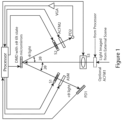
- FIG. 1 shows one embodiment of the smart photonic imager system design of the present invention.
- One camera output port uses a 2-D Photo-Detector Array (PDA) for lower brightness scene detection (PD1) and while the other output port uses a single Point Detector (PD) for higher brightness scene detection (PD2).
- PDA 2-D Photo-Detector Array
- PD Point Detector
- S1, S2 and S3 are lens systems with variable focus controls.
- light from an external scene is imaged onto the DMD plane. This light can pass through an optional electronically controlled ACFM: Attenuator and Color Filter module called ACFM1 so appropriate scene light attenuation and color selection can be implemented if required by the scene imaging application.
- the S1 system can include a set of imaging lenses, including ECVFLs for adaptive focus and image magnification/demagnification controls.
- the Digital Micromirror Device, DMD has a large number of tiny micromirrors (representing an image pixel site) and each micromirror can be set to either a + ⁇ tilt state or a - ⁇ degree tilt state to direct light incident on the pixel to either a + ⁇ tilt state light propagation direction towards lens system S1 or a - ⁇ degree tilt state light propagation direction towards lens system S2.
- Both S1 and S2 lens systems can be designed with a set of fixed focal length lenses plus ECVFLs.
- S1 functions to image the light from the DMD plane to the PD1 plane using the Scheimpflug principle shown in Fig.2 with the appropriate optic devices placement angles with respect to the central axis ray.
- PD1 is a 2D PDA such as a high pixel count CCD or CMOS sensor. Ideally, there should be a 1 to 1 match between the spatial locations of the DMD pixels and the PDA pixels. One could even have an integer multiple of PDA pixels representing 1 DMD pixel.
- the S1 lens system should be designed with the appropriate magnifications (if needed along both its orthogonal axes of pixel x-y layout) to match this DMD plane to PDA plane pixel-to-pixel matching requirement.
- the + ⁇ tilt state imaged light also passes through an electronically controlled ASM: Attenuator and shutter module to both attenuate the overall imaged light but also to control the exposure time on the PD1 sensor.
- the shutter can also completely block the + ⁇ tilt state light from entering the PD1 to prevent unwanted saturation effects.
- the shutter could also implement aperture control so as to spatially restrict certain + ⁇ tilt state light from the image reaching PD1. All these electronically controlled smart optic devices work in unison with the control and image processor system to smartly operate the camera for best scene image capture.
- a fundamental aspect of the Fig.1 design is the use of the DMD + ⁇ tilt state light path for detection of the lower brightness pixels from the input scene image using the PD1 PDA sensor device/output port.
- the DMD - ⁇ degree tilt state light path is used for detection of the higher brightness pixels from the input scene image using the PD2 PD device/output port.
- the S2 lens system functions as a light collection or focusing lens that collects light from the scanning (or point sampling) micromirror on the DMD plane and brings it to focus so it can fall on the PD2 that is a single point detector with high dynamic range.
- the - ⁇ degree tilt state light path passes through an electronically controlled ACFM2 to enable light attenuation and tunable wavelength filtering.
- the electrical signal generated from PD2 can be amplified by the electrical VGA: Variable Gain Amplifier.
- VGA Variable Gain Amplifier
- both PD1 and PD2 can be replaced by an optical fiber bundle and single optical fiber, respectively. In these cases, the fiber bundle and single fiber are terminated with PD1 and PD2, respectively.
- camera output port + ⁇ degree DMD tilt state light and - ⁇ degree DMD tilt state light can be optically amplified by Optical Amplifier devices such as fiber-doped Optical Amplifiers or image intensifier devices.
- the Fig.1 camera design includes two imagers in one unit.
- the + ⁇ degree DMD state light is processed in a Scheimpflug principle-based PDA PD1 camera where the scene pixels are measured in an optical parallel processing arrangement.
- the - ⁇ degree DMD state light is processed within a single PD1 DMD-based imager that uses a serial pixel-by-pixel scan of the image on the DMD plane to record the individual pixel irradiance values that are used to assemble the image irradiance 2-D map via image processing.
- the mode of operation of the Fig.1 camera depends on the scene and its application environment. Take the scenario of a scene containing some high brightness pixels within a lower brightness overall scene. In this case, the Fig.
- the 1 camera can operate as follows. All DMD micromirrors are set to its + ⁇ degree tilt state so all light from the DMD image plane is imaged onto the PDA PD1.
- the image signal produced by PD1 is processed in the image processor to determine the location of the higher brightness pixels.
- the threshold for determining whether a pixel is of high or low brightness can be set by the imager system operator, using either prior scene data or adaptive intelligence using scene sets under viewing.
- the threshold corresponds to the maximum dynamic range of PD1, as any pixel having a brightness which exceeds the dynamic range of PD1 will saturate the PD1, and thus the optical irradiance values of these pixels should be determined by PD2.
- the threshold may be set to correspond to the value of the brightness of a pixel at a location on the object plane of particular interest to the operator.
- micromirrors on the DMD at these image pixel locations are flipped to the - ⁇ degree DMD tilt state.
- PD1 image is again processed by the image processor to make sure that the PD1 viewed image does not contain any high brightness pixels that would have otherwise saturated PD1 or distorted the image seen by PD1. If more pixels with image distortion are obtained, the DMD micromirrors at these pixel locations are also turned to the - ⁇ degree DMD tilt state until PD1 sees a clear image of the partial scene that is free from optical distortions due to bright light zones in the scene. At this stage, all the pixel locations in the target scene and hence the DMD plane are known where the scene has high brightness.
- the DMD tilt state is set to the - ⁇ degree one at a time for these DMD/Image pixel locations so the PD2 can record individual light levels at these high brightness pixels one at a time. While this operation is being conducted, the shutter in the ASM can be used to block any light from reaching PD1 to prevent damage to PD1.
- the Variable optical attenuator in ACFM2 can be engaged if the light levels from the high brightness pixels in the image need further reduction before optical detection at PD2. After all high brightness pixels of the image have been captured by PD2, the image processor records this image data to create the high brightness zone of the original input scene image.
- a full high dynamic range true image of the input scene is created by the image processor.
- This scene is without the distortion expected when using classic PDA cameras such as with CCD and CMOS sensors.
- one camera output port uses a 2-D Photo-Detector Array (PDA) for lower brightness scene detection and while the other output port uses a single Point Detector (PD) for higher brightness scene detection, producing a novel imaging architecture and camera design.
- PDA Photo-Detector Array
- PD Point Detector
- the ECVFL in the S3 lens can change its focal length to image different on-axis focal planes in the image scene.
- a pin-hole can be placed before PD2 to improve out-of-focus light rejection.
- the DMD when operating in its pin-hole pixel scan mode naturally operates as a spatial filtering confocal mode.
- the DMD is programmed with a pinhole in the micromirror + ⁇ degree tilt state so the sampled pinhole light is directed to PD1 while rejected light is sent towards the PD2 direction.
- the DMD is programmed with a pinhole in the micromirror - ⁇ degree tilt state so the sampled pinhole light is directed to PD2 while rejected light is sent towards the PD1 direction.
- Fig.2 shows the proposed smart photonic imager system optical layout design using the Scheinmpflug principle for high focus optical imaging. This design achieves in-focus images on the PD detector planes GB and FC line segments.
- the DMD is placed at location "A” and AH line segment representing the incident light optical axis is normal to the DMD plane.
- the incident light imaging lens system (FM is Fig. 1 ) is placed at location "H” and AH line segment representing the incident light optical axis is normal to the imaging lens system (e.g., FM in Fig.1 ) plane.
- the central optical axis reflected light from the DMD at a given micromirror either travels along the AG line segment direction or the AF line segment direction.
- AD is the object distance
- DG is the image distance that satisfies the imaging condition between A and G using the imaging lens system at D.
- "B” is found by drawing the AB and DB extended lines till they intersect at "B”. Then "B” and “G” are connected by a line BG that defines the correct plane to place the 2-D image sensor (e.g., PD1 in Fig. 1 ).
- a similar approach for the - ⁇ degree state light is used to find the line FC that defines the correct plane to place an imaging PD such as PD2 when light is imaged from the DMD plane to the PD plane.
- S2 functions as a light collection (or focus) lens and PD2 acting as a point detector should be placed on the central axis AF of the system and the distances AG and AF are not necessarily equal.
- ⁇ is the angle between BD and BG.
- ⁇ 2 ⁇ where ⁇ is angle between AH and AF and ⁇ is the binary tilt state angle of the DMD micromirror.
- ⁇ is the angle between CE and CF.
- 90 - ⁇ is the angle between FA and FC and also is the angle the PD2 (e.g., in Fig.3 ) makes with the central axis AF for the - ⁇ state light.
- ⁇ 90 degree, the angle between AE and EC.
- FIG. 3 shows an alternative embodiment (not according to the invention) of the smart photonic imager system design.
- Both output ports use a 2-D PDA.
- One camera output port uses a 2-D PDA for lower brightness scene detection and while the other output port with an electronically controlled optical attenuator uses a 2-D PDA for higher brightness scene detection.
- the 2-D PDA may be a CCD/CMOS/FPA sensor or 2-D fiber-bundle terminated with a lenslet array and PDA.
- the + ⁇ state light camera output port uses a 2-D PDA PD 1 for lower brightness scene detection and while the other the - ⁇ state output port with an electronically controlled Optical Attenuator (OA) uses a 2-D PDA PD2 for higher brightness scene detection.
- OA Optical Attenuator
- OA helps optimize the full dynamic range usage of the PD2.
- Any type of optical amplification can be used for the lower brightness + ⁇ state light such as using an image intensifier device before PD1 and/or fiber-optical amplification when using a fiber bundle.
- the Scheinmpflug principle is applied for both ports for optimal focus imaging.
- the Scheimpflug principle is a prior-art geometrical optics rule that allows one to geometrically calculate the direction of the focus plane of an imaging optical system when the imaging lens plane is not parallel to the object plane (e.g., DMD in this case) or image sensor plane (e.g., PD1 plane).
- the DMD can be operated in a full - ⁇ state light setting so all scene light is sent to PD2 to record with OA control a sequence of higher brightness images.
- These images are then processed by the imager processor to determine the location of the higher brightness pixels in the scene image so next the DMD can be programmed to direct the lower brightness pixels to PD 1.
- the images simultaneously provided by PD1 and PD2 are again processed by the image processor to optimize the locations of the high brightness and lower brightness image pixels so the DMD micromirrors can be optimally controlled to produce the best possible high brightness and lower brightness images by PD2 and PD1, respectively.
- these PD1 and PD2 best quality image are processed by the image processor to stitch together one high quality scene image that shows both the high brightness zones as well as the lower brightness zones.
- All the electronically controlled smart optic devices work together with the image processor to form an adaptive optoelectronic system. The speed of response of the camera system will depend on the response time of the smart optic devices as well as the scene imaging lighting scenario including scene motion characteristics.
- prior art advanced computer vision and image processing techniques can be deployed within the proposed smart camera unit systems to bring software power to the system using the proposed novel optical camera designs to enable scene imaging under extreme light conditions across broadband wavelengths.
- S1, S2, and FM imaging modules have ECVFLs to allow scene image magnification/demagnification controls so one can zoom into scene zones or look are wider scene views.
- the DMD can be used in time modulation mode (as suggested in prior arts) to control scene pixel level light exposure times on the photo-detection devices, in our case, PD1 and PD2 devices.
- the camera system designs shown use incoherent light, coherent light (e.g., from lasers) imaging is also possible using the proposed systems. In this case, the frontend FM imaging lens optics may not be needed in the systems.
- FIG. 4 shows yet another embodiment of the photonic imager system design (not according to the present invention).
- a Variable Beam Splitter (VBS) splits the input scene light into two parallel channels.
- One channel (with an optional variable OA: optical attenuator) uses a 2-D PDA PD1 for lower brightness image scene detection.
- the other channel uses a two PD DMD-based imager for higher brightness scene detection where the PDs are PD2 and PD3.
- the proposed VBS embodiment can be a novel two TIR prism based splitter shown in Figure 4 with the light split ratio controlled by changing fluid type (its refractive index) in the inter-TIR gap.
- An air gap provides 100% scene light directed to the DMD imager that uses two PDs.
- the Fig.4 system provides simultaneous scene imaging by both camera units (i.e., the PDA camera as well as the DMD serial scan camera).
- this DMD camera is robust to temporally light fluctuations during scene serial scan image acquisition as PD2 and PD3 optical irradiance levels are normalized by their total irradiance level reading for each DMD agile pixel scan.
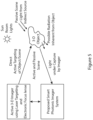
- Figure 5 shows the novel application of the smart photonic system imager for 3-D object capture.
- This proposed dual system arrangement combines the prior-art active laser targeting 3-D imaging system with the proposed smart photonic imager system to produce a novel 3-D image capture system that is suited for high brightness scenes produced by the laser (active lighting) and lower brightness scenes produced by passive lighting conditions such as from the Sun, room lighting, and indirect laser radiation.
- the proposed camera systems are ideally suited for these 3-D imaging scenarios where both bright lasers as well as lower brightness light sources illuminate the target scenes of interest.
- Fig.5 where both active and passive imaging technology is combined in a unique way using the Fig. 1 to Fig.4 proposed novel camera designs that usher in the age of smart photonic systems for extreme lighting conditions imaging using the N.
- the Fig.1 to Fig.5 imagers described in this application operate in the classic photo-detection mode where the light irradiance to be imaged is captured by a starring (i.e., Continuous Wave light photo-charge collection) mode PD (point or multi-pixel) that generates a DC current (or voltage) level per image frame in time that is proportional to the light irradiance (power) level at its specific spatial location on the SLM pixel map.
- a starring (i.e., Continuous Wave light photo-charge collection) mode PD point or multi-pixel
- the SLM e.g., DMD
- the SLM in Figures 1 to 5 are programmed to pick the locations of the incident irradiance map that are sampled one location at a time so DC currents (or voltages) for given locations can be stored in time sequence in the computer for later irradiance map image reconstruction.
- a multi-pixel PD like a CCD
- pixels of the SLM e.g., DMD
- the PDs generate the irradiance map via a DC electrical signal representing the light generated electrical charge.
- 1/f noise i.e., inverse of f
- f the electrical frequency in Hertz.
- f the electrical frequency in Hertz.
- the DMD or the equivalent SLM is programmed as a pixel-location dependent temporal frequency coded incident irradiance light modulator with the optical image reconstruction done via photo-detection at the Intermediate Frequency (IF) band and electrical spectrum processing of the IF band signal, including IF band amplification and filtering, leading to low electronic noise optical imaging.
- IF Intermediate Frequency
- Figure 6 provides an example that is not part of the invention which shows the basic proposed smart photonic imager system concept where the imager is operating in an improved signal-to-noise ratio IF band photo-detection mode by having the irradiance modulating SLM device programmed to act as a spatial position-dependent temporal frequency coded incident irradiance light modulator.
- the SLM device could be replaced by a multi-pixel display device allowing secure image transfer and capture with the PD replaced by a guiding collection optic (e.g., optical fiber) terminated with the point PD.
- a guiding collection optic e.g., optical fiber
- the photo-detected signal is undergoing electronic spectrum analysis (such as via the Fast Fourier Transform (FFT) algorithm), e.g., within dedicated electronics and signal processing software to produce the decoding from a specific IF value to a specific SLM pixel position where the incident light pattern had first interacted with the SLM.
- FFT Fast Fourier Transform
- the SLM is shown operating with 3 pixels (can be any shape, location and sized zones on the SLM), each time modulating its specific pixel incident light irradiance at a different temporal frequency, so pixel 1 at f1 Hz, pixel 2 at f2 Hz, and pixel 3 at f3 Hz.
- the remaining pixels in the SLM operate in the classic starring mode and are NOT time modulated.
- a transmissive SLM is shown in Fig.6 , although a reflective SLM such as a DMD can also be used as shown in Fig.7 .
- N pixels of the SLM are time modulated in irradiance with all the light after the SLM collected by a collection lens S1 so that all light falls on a point PD.
- the SLM is operated such that only the 3 chosen pixels on the SLM let light through with time modulation of the irradiance at these pixel locations while the other pixels completely block the light. This is the case where the SLM pixels act as digital on/off time modulators.
- analog irradiance time modulation of the SLM can also be deployed.
- the PD chosen has an operational electrical bandwidth exceeding the highest temporal modulation frequency of the SLM pixel, so is greater than f3 if f3 is the highest frequency in f3,f2,f1 Hz.
- the electrical current produced by the PD will have a DC current term (because intensity modulation of pixels requires light modulation around a bias irradiance level); plus the current contains electrical signals at the f1,f2, f3 Hz frequencies.
- the incident light irradiance on the SLM is considered an incoherent incident irradiance (e.g., from a white light source such as from the Sun or light bulbs)
- the individual pixel temporally modulating irradiances contributions naturally add up in the PD photo-detection process without optical interference effects, thus leading to a linear addition of the 3 different temporal frequency electrical current signals, much like a simple Fourier series like sum producing independent spectral lines in the IF domain.
- This current after IF band electronic amplification and IF band filtering is fed to a FFT electronic implementer or IF band spectrum analyzer that produces the needed RF power spectrum of the total electrical current from the point PD.
- the photo-detected current (or voltage) can be sampled by an Analog-to-Digital (ADC) converter and the digital bits are processed by the FFT algorithm software within a computer.
- ADC Analog-to-Digital
- an imager design optical detection mode for the smart imagers is realized where the IF spectrum analysis of the PD provided electrical signal can simultaneously produce all the relative irradiance values for the time modulated pixel locations in the incident irradiance map leading to low noise detection of an image.
- the imager can be calibrated to provide true irradiance maps versus relative irradiance values.
- time modulating pixel location sizes, shapes, temporal frequencies, modulation type (digital, analog, mixed analog-digital) and numbers (e.g., look at 3 pixels simultaneously or 1 million pixels or 1 pixel at a time) depends on the application for the smart imager.
- modulation type digital, analog, mixed analog-digital
- numbers e.g., look at 3 pixels simultaneously or 1 million pixels or 1 pixel at a time
- irradiance modulation of the pixel on the SLM in analog or gray-scale mode such as by using an analog liquid crystal SLM gives sinusoidal temporal intensity modulation while using the digital micromirrors on-off mode of the DMD gives on/off square wave like temporal modulations for the incident irradiance on the SLM.
- prior-art optical systems have deployed a time modulating shutter on an entire light beam to produce a photo-detected signal on an IF to extract weak signals such as during material characterization (see for example A. Nag, A. K. De, and D. Goswami, "Two-photon cross-section measurements using an optical chopper: z-scan and two-photon fluorescence schemes," J. Phys. B At. Mol. Opt. Phys., vol. 42, no. 6, p. 065103, 2009 ).
- Fig.6 shows how one can code irradiance image space with temporal frequencies to realize an optical imager design where IF spectrum analysis of photo-detected electrical signal provides the near instantaneous spatial irradiance mapping of the optical image (light pattern) incident of a time modulating multi-pixel zone SLM.
- This powerful new idea in smart imaging on the photo-detection side of imager design can produce new capabilities for optical imagers over many fields of science and engineering.
- Choice of temporal frequencies f1, f2, ..,fN can also be optimized to reduce non-linear processing effects including intermodulation products and pixel overlapping harmonics.
- electronic amplification and filtering can be used to reject known frequency noise signals to produce the desired frequency spectrum power data to provide the sampled image space irradiance map.
- any stray light reaching the PDs in the Fig.6 and Fig.7 imagers will not have undergone IF modulation via the DMD/SLM device, and will therefore show up as a DC signal in the PD electrical output. This can be easily filtered out to produce a lower noise output signal from the desired irradiance map that is IF modulated on the DMD/SLM plane.
- coherent electrical detection methods after photodetection can be used to pick up and electrically and coherently amplify imaged irradiance levels that would otherwise be deeply buried in system noise.
- One such suitable method is lock-in amplification.
- the SLM pixel time modulation drive signals are generated via the SLM image generation electronics that can provide mutually coherent pixel drive signals as they are generated from the same system clock in the SLM drive electronics.
- this coherent clock i.e.
- the fundamental carrier that electrically drives the SLM pixels can be used as the phase synchronizing and carrier mixing signal input for a lock-in mode amplifier that is also fed by the signal produced by the point PD in the imager. It is also possible to use a combination of lock-in amplification and standalone amplification on a SLM pixel basis. In other words, certain pixels (such as for example low irradiance level signals buried in optical noise) in the irradiance map being imaged may require coherent phase-sensitive lock-in amplifier-based detection, while other pixels (such as for example those pixels with a high brightness level) are adequately resolved using non-phase sensitive standard IF amplification without using a phase-locking carrier signal from the SLM pixel driver electronics. Note that with phase sensitive dual channel lock-in detection, a complex domain (in-phase and quadrature) FFT IF spectrum analysis can be conducted for the photo-detected signal from the point PDs, leading to phase sensitive optical imaging capabilities.
- the light irradiance incident on the SLM is coherent (e.g., from a laser source)
- simultaneous detection of multiple pixel light on the same zone of the PD can generate optical field-based interference effects.
- These interference effects can be nulled to produce true linear summation of the irradiance contributions to the photo-detected current.
- coherent light from different pixels of the SLM produce an interference fringe pattern on the PD.
- the interference term is averaged out to zero leaving only the linear sum of the irradiance values from the individual pixels, giving the desired output signal current containing the sum of the frequencies time modulating the different pixels.
- the pixel locations at any instant can be picked to produce fast enough spatial frequencies on the PD active area to produce adequate averaging of many fringe cycles.
- Another method to counter interference effects is to place a random optical phase screen (like a diffuser) after the SLM that puts a random optical phase to the optical fields at the different time modulating pixel locations. By doing so, the interference term nulls out during the PD photo-detection process.
- Fig.6 An important outcome of the smart imager design of Fig.6 is that the physical size of the pixel chosen for time modulation can be extremely small and does not fundamentally have to obey the traditional imaging system Abbe diffraction limit for transverse dimension best resolution possible for the detection optical image. So one can envision the SLM to have extremely small (much less than optical wavelength) pixel zones that can undergo optical irradiance time modulation allowing an image of the irradiance pattern interacting with the SLM to be created that breaks the classic Abbe resolution limit. This is because the spatial irradiance information of the SLM incident image that is mapped onto a position coded temporal frequency map and then resolved by the temporal frequency spectrum analysis is no longer connected to fundamental Abbe spatial diffraction limits of an optical imaging system.
- the FFT spectrum analysis system must resolve two independent pixel modulating frequencies closest to one another and these can be chosen far enough away that they can be resolved by the FFT spectrum analysis deployed in the imager.
- a number of SLM device technologies could realize the desired pixel-level time modulator such as Silicon NEMS (Nano-Electro-Mechanical Systems), Quantum Dot and quantum well devices, Nano-membrane devices, nanopolymer-based liquid crystal modulators, nano-liquid devices, and other nano-material based SLMs including bio-molecular material (e.g., fluorescent proteins and organic small-molecule fluorophores) based SLMs.
- bio-molecular material e.g., fluorescent proteins and organic small-molecule fluorophores
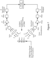
- Fig.7 shows an implementation of the Fig.6 system concept using the DMD as the SLM.
- Two arms of the detection system are formed, each with their point PDs, IF amplifiers, IF filters and IF band FFT implementators. Data from both detection arms is used to reconstruction a robust optical irradiance map using the two detected RF spectra of the two independent photo-detected currents.
- Such a system always displays built-in redundancy and fault-tolerance given two photo-detected signals are detected although a single PD arm can produce the desired image map.
- the principle of Fig.6(a) also works for the other proposed Fig.1 to Fig.5 imager systems. When multi-pixel PDs are used with independent PD pixel currents, these different electrical current/voltage outputs should be summed before undergoing spectrum analysis.
- Fig.6 shows the irradiance pattern to be imaged as an incident light pattern striking the SLM device.
- the SLM device is replaced by an optical image generation device such as an optical display device with multiple pixels where each pixel can be electronically (or optically) controlled to produce pixel-based irradiance modulation in time.
- each pixel is allocated a specific temporal modulation frequency and irradiance modulation format so multiple pixels undergoing simultaneous irradiance modulation in time can be identified in pixel spatial location using the earlier described IF spectrum processing.
- the Abbe diffraction limit of the classic optical system no longer prevents full recovery and image reconstruction of the pixel resolved irradiance map originally displayed on the display device.
- nano-LED array, nano-laser array, a quantum dot modulator array, or any other display device where the emission pixel size is under the classic optics resolvable pixel size, will still be spatially resolved on a super-pixel basis using the proposed IF spectrum processing.
- the Fig.6 PD can also be replaced by an appropriate light capture optic (e.g., an optical waveguide like an optical fiber) so the captured light emitting from the display device is transported to another physical location before being converted via the PD to an IF spectrum signal, thus forming an optical communications data link where the data is the image on the display that is undergoing pixel-based IF coded irradiance modulation.
- an appropriate light capture optic e.g., an optical waveguide like an optical fiber
- the design of the light capture optic e.g., lens S1 in Fig.6 and an optical fiber instead of the PD in Fig.6 ) with respect to the display device determines any windowing of the captured irradiance from the different pixels in the display.
- the effect of the windowing can be calibrated into the IF signal processing to recover the true un-windowed irradiance pattern on the display.
- the IF band can occupy a variety of spectral bands in the RF spectrum from Hertz to many GHz and even higher.
- the optical communications data link proposed also becomes an extremely secure data link as first a user codes the image pixels with temporal frequencies and their given modulation formats, then the user at the receiver end must know the true frequency codes and modulation formats to correctly decode the PD generated IF data to recover the true image.
- the Fig.6 system not only forms an optical imager, it also forms a display capture systems that can function as a secure optical communication data link.
- a special scenario of the Fig.6 design is when the aperture of the display device matches the aperture of the light collection optic so a face-to-face coupling of the display chip can be implemented with the capture optic like with the core of the optical fiber.
- the Fig.6 lens S1 is not used, thus implementing lensless image transfer, and light from all the pixels from display chip goes straight into the fiber which delivers it to the PD attached to the other end of the fiber. So a super-compact image transmission guide is formed using a single fiber and single PD with single miniature display device, e.g., nano-LED array.
- FIG.6 design Another special scenario of the Fig.6 design is when an object under observation is placed directly on the SLM chip cover glass, or adjacent to the display device (i.e., SLM location in Fig.6 ).
- a biological specimen slide can be placed almost in contact with the display or SLM chip that is acting as an IF-coded point light sources in a multi-pixel grid under the sample slide that is being imaged, or perhaps as a thin film containing the sample to be imaged, e.g., via a sample in a fluidic channel on the SLM.
- the compact lensless i.e.
- the point PD sits atop the sample slide to collect light from all pixels from the SLM grid, providing the IF coded pixel location specific point light sources.
- a plurality of stacked thin fluidic surface layers are placed atop the SLM chip.
- only one fluidic layer channel at one time contains the sample to be imaged, with the other fluidic layers filled with a refractive index matching fluid, so that the light passing through the stacked layers of fluids essentially does not see the other fluidic surface channel boundaries.
- this channel must be fed with the sample while all the other channels interacting with the light should contain the index matching fluid.
- defocus algorithms in imaging processing can be used if needed to improve focus restoration for the near-field acquired images via this shadow-type lensless imaging system (i.e., when not using lens S1 in Fig.6 ), when sample layers are not directly in the close near field of the SLM pixel plane. It is important to note that adjacent pixels in the SLM can be time modulated in time sequence to reduce adjacent pixel crosstalk picked up from the sample under view.
- the axial plane subjected to imaging in the 3-D object can be selected using various confocal microscopy techniques. Because the display or SLM pixels can be smaller than the Abbe limit of the optical capture system, imaging that beats the Abbe transverse resolution can still be achieved. Again, time modulation of the display or SLM device (needs the use of a light source next to the SLM chip) is used with IF spectrum processing to recover the image plane under observation, thus implementing nanoscopy (breaking the Abbe limit) on the transverse pixel plane.
- a pixel of the display device can be a wavelength tunable light source either inherently or by using a wavelength tuning filter at the pixel.
- pixels in the display can be designed to be simultaneously emitting pixel specific wavelengths. Either way, electronic control of emitted wavelength at a display pixel provides another mechanism for image irradiance reconstruction (of object plane physically adjacent to display) on a many simultaneous pixel detection basis level as pixel locations are wavelength coded in addition to being IF coded as each display pixel operates as an emitted light irradiance modulator in time.
- the display plane first imaged on to an object plane under observation and then the object plane wavelength and IF coded irradiance map being collected by the collection lens so this multi-wavelength light falls on the point PD.
- the object plane wavelength and IF coded irradiance map being collected by the collection lens so this multi-wavelength light falls on the point PD.
- classic imaging lens optics is being used between the display plane and the object plane, one cannot break the Abbe diffraction limit.
- the pixels in the display are not coherently synchronised such as when using an LED array or a laser array with independent laser cavities per pixel, the multi-wavelength light detected by the point PD does not suffer fundamentally from optical interference effects.
- the display simultaneously uses multiple wavelengths or multiple wavelength bands at the same time, one can deploy dispersive optics (gratings, dichroic beam splitters, prisms, fiber gratings, photonic crystal devices, etc) to separate the colors before photo-detection so independent point PDs can be used, say for red, green, and blue color bands allowing multi-spectral imaging for the visible band.
- dispersive optics gratings, dichroic beam splitters, prisms, fiber gratings, photonic crystal devices, etc
- Tuning of the display wavelength in time can also be used to provide multi-color imaging, in this case, simply by using the same point PD for all colors, but one color at a time.
- the display device in Fig.6 imager design emit the exact same wavelength for each pixel in the device and use of different wavelength-coded pixels along with the IF coding of display pixels can produce powerful signal processing capabilities and features for image recovery of object plane under view.
- prior-art confocal microscopy methods can be engaged to deliver 3-D imaging capabilities.
- a new hybrid design imager that is pixel efficient can be realized by combining the Fig.6 imager using IF pixel coding for chosen pixels with the DC current photo-detection-based prior-art imagers.
- a Variable Beam Splitter to create two independent imaging channels, one for the classic DC current-based imager and one for the imager with pixel coding using specific IF values.
- a smart imager system is realized using a combination or hybrid imager design suited for extreme conditions optical imaging, a theme of the proposed invention of a smart agile pixel within the sampling SLM/display device irradiance plane.
- each photo-detector (point or 2-D array) in the proposed smart imager designs, one can place a Polarizing Beam Splitter (PBS) to separate the vertical and horizontal linear components of the light polarizations coming from the optical irradiance map subjected to imaging by the optical system.
- PBS Polarizing Beam Splitter
- a pair of PDs is used after the PBS to detect each orthogonal linear polarization separately.
- the proposed imager can extract polarization information of the imaged optical irradiance.
- the Fig.6 design enables optical imaging that can defy the classic Abbe limit; in addition, the innovation also provides a mechanism for very low noise highly sensitive image extraction via the IF (radio frequency) signal processing platform with advanced applications leading to secure data transmission and image capture.
- IF radio frequency
- the mature radio frequency (RF) and microelectronics industry and their chip innovations are fully exploited to extract the super-resolution optical irradiance data maps that would otherwise be unseen using classic diffraction limited optics.
- Figure 8 shows an alternate generalized operation of the Smart Photonic Imaging System camera unit using image optical irradiance pixel position coding of the SLM based modulation using spread spectrum time-frequency codes, also called Code Division Multiple Access (CDMA).
- CDMA Code Division Multiple Access
- FDMA Frequency Division Multiple Access
- the proposed CDMA pixel coding method gives each pixel a spread spectrum in the electrical frequency domain.
- FIG 8 shows the optical design and operations of the CAOS imager of the invention.
- Incident optical irradiance to be imaged strikes the 2-D transmissive pixelated SLM (a reflective SLM can also be deployed using a different optical systems geometry).
- Each pixel in the SLM is used to time modulate the pixel incident optical irradiance using a binary code sequence that acts as a irradiance data spreading signal that has a spread spectrum in the electrical frequency domain.
- Such coding of pixels in the SLM follows the CDMA data encoding approach commonly used in wireless cellular mobile communications.
- N pixels in the SLM are simultaneously time modulated by CDMA codes with optimally all codes mutually orthogonal (like Walsh codes) to each other so decoding of pixel irradiances is possible with maximum autocorrelation values and minimum cross-correlation values.
- the individual bit time of the M-bits code depends on the time modulation response of the SLM device technology with bit bandwidths ranging from sub-Hz to even 100 GHz or more.
- the length M of the code also depends on the CAOS imager application and the number N of pixels the imager desires to detect simultaneously in time using the CDMA technique.
- SNR signal-to-noise
- increasing M improves signal processing gain via the time integrated correlation operation. This is the same reason why very weak RF signals buried in noise and picked up by mobile cell phone can be detected by a high sensitivity CDMA receiver in a modern phone. This same principle is deployed in the pixel irradiance decoder of the CAOS imager.
- the photo-detected signal i(t) in Fig.8 passes through an Electronic Amplifier (EA) and Electronic Filter (EF) to enhance the SNR of the multi-pixel CDMA signal i(t) before it enters the Data Sampler (DS).
- EA Electronic Amplifier
- EF Electronic Filter
- the DS can be an Analog-to-Digital Converter (ADC).
- the lens S1 may have a transverse optical resolution that is unable to resolve the pixel size of the SLM, yet the CAOS imager via CDMA pixel encoding and decoding can fully resolve the SLM pixel-based irradiance values illuminating the pixelated SLM.
- Such power for the CAOS imager derives from the fact that pixel-to-pixel irradiance separation is NOT done in the spatial optical processing domain where optical diffraction fundamentally limits optical system imaging resolution. Instead, the CAOS imager resolves the pixel-to-pixel based irradiance in the electrical time-frequency signal processing domain that does NOT suffer from inherent optical spatial diffraction limits such as the Abbe transverse resolution limit.
- the CAOS imager can still resolve this extremely small pixel size on the SLM using proposed CDMA signal processing using the appropriate CDMA codes.
- a lensless imager can be realized for the CAOS imager by eliminating the S1 lens between the SLM and PD. In this case, the PD is placed adjacent to the SLM so the entire PD active area overlaps the SLM.
- Fig.9 shows an alternate design of the CAOS imager where the SLM is replaced by a 2-D pixelated display device or a 2-D light source array device such as a 2-D laser array or 2-D LED array.
- the object to be optically imaged is placed adjacent to the display/light source array device such as by placing a microscope slide on the SLM device.
- the sample to be imaged is directly placed on the cover glass of the display chip.
- the Fig.9 imager produces a multi-pixel CDMA signal on an IF (Intermediate Frequency) carrier of f c Hz.
- IF Intermediate Frequency
- Fig.9 shows that all pixels modulated on the display use the same IF of f c Hz.
- the Fig.9 imager design can deploy mobile phone type IF-based pixel decoding processing.
- This IF-based signal processing is also similar to RF radar receiver correlation signal processing that can produce exceptional SNR and large processing gains to detect extremely weak irradiance signals (buried in deep noise) from the pixels of the imaged light map.
- frequency hopping codes across an RF band to modulate the pixels can also be used and in this case the f c values are different for the different pixels, although, a mid-band f c Hz value is considered as the IF for signal processing hardware selection.
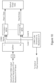
- Fig.10 shows a proposed parallel processing signal correlation architecture implemented in software or dedicated electronic hardware to recover the CDMA sampled optical image.
- the correlation operations can be at baseband or IF based on whether the Fig.8 or Fig.9 designs are used.
- the DS is a ADC.
- the DS is an RF mixer connected to a local RF oscillator. After the DS, the sampled multi-pixel CDMA signal is split into N replicas corresponding to N pixels that were simultaneously time modulated at the SLM/display device.
- Each CDMA signal replica is fed to a time integrating correlator also fed with its pixel specific CDMA code.
- the N outputs of the correlators provide the N-pixel irradiance map that was originally sampled at the SLM/Display image plane where the light map was originally present.
- the correlators function as an array of matched filters, each with its own match filter function corresponding to its pixel specific CDMA code.
- a hybrid processor can also be engaged that uses both dedicated RF electronics and digital computing machines to implement the pixel-based encoding and decoding operations for the CAOS imager.
- I In-Phase
- Q Quadrature
- Fig.10 for simplicity only shows the I-processing chain in the decoding operations.
- the pixel encoder and pixel decoder can be mutually phase-coherent using the same time-base to generate the CDMA codes for both SLM/display pixel encoding and multi-pixel CDMA signal decoding to recover the pixelated optical irradiance map incident at the SLM/display plane.
- CAOS imagers are spread spectrum signals in the electrical frequency domain. This is completely unlike classic CCD and CMOS imagers that operate in starring mode collecting photo-charge that produces a DC current from the pixels and hence is subjected to excess 1/frequency or 1/f noise in the image generation electronics.
- 1/f noise is reduced greatly, in particular, when an IF is used in the decoding process to recover pixel irradiance information from the multi-pixel CDMA signal produced by the PD.
- Polarization Division Multiple Access (PDMA) techniques can be used to double the pixel count for simultaneous CDMA operations in the CAOS imager using 2 independent signal processing channels, one for linear p-polarized light and one for linear s-polarized light with channels optically separated using a polarization beam splitter device.
- PDMA Polarization Division Multiple Access
- Both the CDMA and FDMA pixel coding smart imager designs allow multiple pixels in the irradiance map under observation to be processed simultaneously, saving significant time to produce a desired image. This is in contrast to the TDMA or Time Division Multiple Access imager where the irradiance map on the SLM (e.g., DMD) is scanned one pixel at a time, thus requiring larger time duration to complete the image map, although with minimal inter-pixel crosstalk as only one pixel irradiance data is detected by the PD at any instant.
- SLM e.g., DMD
- the proposed smart imager can operate in a hybrid mode based on the application, and can be using a combination of CDMA, FDMA, PDMA, and TDMA modes of operations to match the needs of the imaging environment and its specific application.
- the embodiments in the invention described with reference to the drawings comprise a computer apparatus and/or processes performed in a computer apparatus.
- the invention also extends to computer programs, particularly computer programs stored on or in a carrier adapted to bring the invention into practice.
- the program may be in the form of source code, object code, or a code intermediate source and object code, such as in partially compiled form or in any other form suitable for use in the implementation of the method according to the invention.
- the carrier may comprise a storage medium such as ROM, e.g. CD ROM, or magnetic recording medium, e.g. a floppy disk or hard disk.
- the carrier may be an electrical or optical signal which may be transmitted via an electrical or an optical cable or by radio or other means.
Landscapes
- Engineering & Computer Science (AREA)
- Multimedia (AREA)
- Signal Processing (AREA)
- Physics & Mathematics (AREA)
- General Physics & Mathematics (AREA)
- Human Computer Interaction (AREA)
- Studio Devices (AREA)
- Microscoopes, Condenser (AREA)
- Transforming Light Signals Into Electric Signals (AREA)
- Mechanical Light Control Or Optical Switches (AREA)
Claims (11)
- Verfahren zum Durchführen von optischer Bilderfassung mit hohem Dynamikbereich einer Szene mit Hilfe von optischen Geräten, die ein 2D-SLM-(Spatial Light Modulator)-Gerät, ein 2D-PDA (Photodetektor-Array), einen Punktdetektor, ein erstes Linsensystem und ein zweites Linsensystem umfassen, wobei die Platzierung der optischen Geräte nach dem Scheimpflug-Prinzip erfolgt, wobei das Verfahren Folgendes beinhaltet:Abbilden von einfallendem Licht von einer Szene auf eine Objektebene des 2D-SLM-(Spatial Light Modulator)-Geräts, wobei der SLM ein DMD (Digital Micromirror Device) umfasst;wobei das Verfahren durch die folgenden Schritte gekennzeichnet ist:Abbilden von Licht aus der Objektebene des DMD mit dem ersten Linsensystem (S1) auf das 2D-Photodetektor-Array (PD1) nach dem Scheimpflug-Prinzip;Bestimmen der Positionen von Pixeln in der Objektebene in einem ersten Helligkeitsbereich aus dem vom 2D-Photodetektor-Array (PD1) erzeugten Bildsignal;Abbilden von Licht aus der Objektebene des DMD mit dem zweiten Linsensystem (S2) zur Fokussierung auf den Punktdetektor (PD2) nach dem Scheimpflug-Prinzip;Erfassen, durch den Punktdetektor (PD2), nur optischer Bestrahlungsstärkewerte der Pixel im ersten Helligkeitsbereich, die von der Objektebene des DMD reflektiert werden, um ein erstes erfasstes Bild zu erzeugen;Erfassen, durch das 2D-Photodetektor-Array (PD1), von optischen Bestrahlungsstärkewerten von Pixeln in einem zweiten Helligkeitsbereich, die von der Objektebene des DMD reflektiert werden, um ein zweites erfasstes Bild zu erzeugen, wobei der erste Helligkeitsbereich höher ist als der zweite Helligkeitsbereich; undErzeugen einer Karte der optischen Bestrahlungsstärke mit hohem Dynamikbereich der Szene durch Kombinieren des ersten erfassten Bildes und des zweiten erfassten Bildes zu einem einzigen Bild;wobei der Schritt des Bestimmens der Positionen der Pixel in der Objektebene mit höherer Helligkeit im ersten Helligkeitsbereich Folgendes beinhaltet:Vergleichen des Bestrahlungsstärkewertes jedes Pixels in der Objektebene mit einem vorbestimmten Bestrahlungsstärkeschwellenwert; undFeststellen, dass ein Pixel von höherer Helligkeit ist, wenn sein Bestrahlungsstärkewert höher als der Bestrahlungsstärkeschwellenwert ist, wobei die Pixel von geringerer Helligkeit im zweiten Helligkeitsbereich den Pixeln in der Objektebene entsprechen, für die festgestellt wird, dass sie einen Bestrahlungsstärkewert haben, der gleich dem oder niedriger als der vorbestimmte(n) Bestrahlungsstärkeschwellenwert ist.
- Verfahren nach Anspruch 1, wobei das Verfahren ferner Folgendes beinhaltet:Einstellen der DMD-Mikrospiegel in ihren -θ-Grad-Kippzustand, um abgetastetes Licht von der Objektebene zum Erfassen der optischen Bestrahlungsstärkewerte der Pixel mit höherer Helligkeit zu lenken;Einstellen der DMD-Mikrospiegel in ihren +θ-Grad-Kippzustand, um abgetastetes Licht von der Objektebene zum Erfassen der optischen Bestrahlungsstärkewerte der Pixel mit geringerer Helligkeit zu lenken; undBestimmen der Positionen der Pixel in der Objektebene mit höherer Helligkeit durch Einstellen der DMD-Mikrospiegel in ihren -θ-Grad-Kippzustand und Erfassen der Pixel in der Objektebene mit größerer Helligkeit.
- Verfahren nach einem der vorherigen Ansprüche, wobei der Schritt des Abbildens des einfallenden Lichts von einer Szene auf die Objektebene ferner das Abbilden verschiedener Brennebenen auf der Achse in der Bildszene beinhaltet, um 3D-Abbildung bereitzustellen.
- Verfahren nach einem der vorherigen Ansprüche, das ferner das Trennen der vertikalen und horizontalen linearen Komponenten der Lichtpolarisationen vor dem Erfassen der optischen Bestrahlungsstärkewerte beinhaltet.
- Verfahren nach einem der vorherigen Ansprüche, das ferner das Betreiben des SLM im Zeitmodulationsmodus beinhaltet, und wobei der SLM ein optisches Mehrpixel-Anzeigegerät umfasst, und wobei das Verfahren ferner das Zeitmodulieren der Einfallslichtbestrahlungsstärke von einem oder mehreren der Pixel auf der Objektebene mit einer bestimmten zeitlichen Frequenz beinhaltet.
- Verfahren nach Anspruch 5, das ferner das unabhängige Steuern der Zeitmodulation der Einfallslichtbestrahlungsstärke für jedes der ein oder mehreren Pixel beinhaltet, und wobei jedes Pixel mit einer anderen ausgewählten Frequenz zeitmoduliert wird.
- Verfahren nach Anspruch 5 oder Anspruch 6, wobei die Schritte des Erfassens der optischen Bestrahlungsstärkewerte ferner die folgenden Schritte beinhalten:Zwischenfrequenz-(ZF)-Bandverstärken und -filtern jedes erkannten zeitmodulierten Signals; undDurchführen einer ZF-Bandspektrumanalyse des gefilterten Signals, um die relativen optischen Bestrahlungsstärkewerte für die zeitmodulierten Pixelpositionen in der Objektebene zu erfassen, um das optische Bild in der Objektebene zu rekonstruieren.
- Verfahren nach Anspruch 5, wobei der SLM ein optisches Mehrpixel-Raummodulationsgerät umfasst, und wobei das Verfahren ferner die gleichzeitige Zeitmodulation der Einfallslichtbestrahlungsstärke von einem oder mehreren der Pixel auf dem SLM mit Hilfe einer CDMA-(Code Division Multiple Access)-Binärcodesequenz beinhaltet, um jedem der ein oder mehreren Pixel ein Spreizspektrum im elektrischen Frequenzbereich zu verleihen.
- Verfahren nach Anspruch 8, wobei die Schritte des Erfassens der optischen Bestrahlungsstärkewerte ferner die folgenden Schritte beinhalten:Verstärken und Filtern eines Mehrpixel-CDMA-Signals, das die Summe der ein oder mehreren zeitmodulierten Pixel umfasst;Datenabtasten des gefilterten Mehrpixel-CDMA-Signals; undDurchführen einer CDMA-Signalverarbeitung an dem datenabgetasteten Signal.
- Verfahren nach Anspruch 9, wobei der Schritt des Durchführens von CDMA-Signalverarbeitung an dem datenabgetasteten Signal ferner Folgendes beinhaltet:Aufteilen des Mehrpixel-CDMA-Signals in ein oder mehrere Replikate, die den ein oder mehreren zeitmodulierten Pixeln entsprechen; undEingeben jedes der ein oder mehreren Replikate in einen entsprechenden Zeitintegrationskorrelator, der mit dem mit diesem Pixel assoziierten CDMA-Code versorgt wird, wobei der Ausgang des Korrelators dem optischen Bestrahlungsstärkewert dieses Pixels entspricht.
- Vorrichtung zum Durchführen von optischer Bilderfassung mit hohem Dynamikbereich einer Szene, die Folgendes umfasst: optische Geräte, die Folgendes umfassen: ein 2D-SLM-(Spatial Light-Modulator)-Gerät, ein 2D-PDA (Photodetektor-Array), einen Punktdetektor, ein erstes Linsensystem und ein zweites Linsensystem, wobei die optischen Geräte nach dem Scheimpflug-Prinzip platziert sind;Mittel zum Abbilden von einfallendem Licht von einer Szene auf eine Objektebene des 2D-SLM-(Spatial Light Modulator)-Geräts, wobei der SLM ein DMD (Digital Micromirror Device) umfasst;wobei die Vorrichtung dadurch gekennzeichnet ist, dass sie Folgendes umfasst:Mittel zum Abbilden von Licht aus der Objektebene des DMD mit dem ersten Linsensystem (S1) auf das 2D-PDA (Photodetektor-Array) (PD1) nach dem Scheimpflug-Prinzip;Mittel zum Bestimmen der Positionen von Pixeln in der Objektebene in einem ersten Helligkeitsbereich aus dem vom 2D-Photodetektor-Array (PD1) erzeugten Bildsignal;Mittel zum Abbilden von Licht aus der Objektebene des DMD mit dem zweiten Linsensystem (S2) auf den Punktdetektor (PD2) nach dem Scheimpflug-Prinzip;Mittel zum Erfassen, durch den Punktdetektor (PD2), nur optischer Bestrahlungsstärkewerte der Pixel im ersten Helligkeitsbereich, die von der Objektebene des DMD reflektiert werden, um ein erstes erfasstes Bild zu erzeugen;Mittel zum Erfassen, durch das 2D-Photodetektor-Array (PD1), von optischen Bestrahlungsstärkewerten von Pixeln in einem zweiten Helligkeitsbereich, die von der Objektebene des DMD reflektiert werden, um ein zweites erfasstes Bild zu erzeugen, wobei der erste Helligkeitsbereich höher ist als der zweite Helligkeitsbereich; undMittel zum Erzeugen einer Karte der optischen Bestrahlungsstärke mit hohem Dynamikbereich der Szene durch Kombinieren des ersten erfassten Bildes und des zweiten erfassten Bildes zu einem einzigen Bild;wobei das Mittel zum Bestimmen der Positionen der Pixel in der Objektebene mit höherer Helligkeit im ersten Helligkeitsbereich Folgendes umfasst:Mittel zum Vergleichen des Bestrahlungsstärkewertes jedes Pixels in der Objektebene mit einem vorbestimmten Bestrahlungsstärkeschwellenwert; undMittel zum Feststellen, dass ein Pixel von höherer Helligkeit ist, wenn sein Bestrahlungsstärkewert höher als der Bestrahlungsstärkeschwellenwert ist, wobei die Pixel von geringerer Helligkeit im zweiten Helligkeitsbereich den Pixeln in der Objektebene entsprechen, für die festgestellt wird, dass sie einen Bestrahlungsstärkewert haben, der gleich dem oder niedriger als der vorbestimmte(n) Bestrahlungsstärkeschwellenwert ist.
Applications Claiming Priority (3)
| Application Number | Priority Date | Filing Date | Title |
|---|---|---|---|
| GBGB1418678.7A GB201418678D0 (en) | 2014-10-21 | 2014-10-21 | Smart Photonic Imaging Method and Apparatus |
| GB201422684 | 2014-12-18 | ||
| PCT/EP2015/074419 WO2016062785A2 (en) | 2014-10-21 | 2015-10-21 | Smart photonic imaging method and apparatus |
Publications (3)
| Publication Number | Publication Date |
|---|---|
| EP3210372A2 EP3210372A2 (de) | 2017-08-30 |
| EP3210372C0 EP3210372C0 (de) | 2023-07-19 |
| EP3210372B1 true EP3210372B1 (de) | 2023-07-19 |
Family
ID=54545074
Family Applications (1)
| Application Number | Title | Priority Date | Filing Date |
|---|---|---|---|
| EP15794832.4A Active EP3210372B1 (de) | 2014-10-21 | 2015-10-21 | Intelligentes photonisches bildgebungsverfahren und vorrichtung |
Country Status (3)
| Country | Link |
|---|---|
| US (1) | US10721411B2 (de) |
| EP (1) | EP3210372B1 (de) |
| WO (1) | WO2016062785A2 (de) |
Families Citing this family (17)
| Publication number | Priority date | Publication date | Assignee | Title |
|---|---|---|---|---|
| GB201701296D0 (en) | 2017-01-26 | 2017-03-15 | Univ College Cork - Nat Univ Of Ireland | Smart coded access optical sensor |
| CN107121709B (zh) * | 2017-06-01 | 2023-07-25 | 华南师范大学 | 一种基于压缩感知的对象成像系统及其成像方法 |
| JP7025940B2 (ja) * | 2018-01-26 | 2022-02-25 | 京セラ株式会社 | 電磁波検出装置および情報取得システム |
| JP7260966B2 (ja) * | 2018-02-19 | 2023-04-19 | 京セラ株式会社 | 電磁波検出装置 |
| CN108520551B (zh) * | 2018-03-30 | 2022-02-22 | 苏州蜗牛数字科技股份有限公司 | 实现光贴图动态光照的方法、存储介质及计算设备 |
| CN110445955B (zh) * | 2018-05-02 | 2021-02-26 | 杭州海康威视数字技术股份有限公司 | 一种补光系统及摄像机 |
| US10872257B2 (en) * | 2018-06-06 | 2020-12-22 | Weltrend Semiconductor Inc. | Barcode detection method and barcode detection system for increasing detection efficiency |
| TWI676936B (zh) * | 2018-06-06 | 2019-11-11 | 偉詮電子股份有限公司 | 條碼偵測方法及條碼偵測系統 |
| CN108965838B (zh) * | 2018-06-29 | 2020-04-03 | 长春理工大学 | 高动态范围景象生成方法、装置及系统 |
| JP7246151B2 (ja) * | 2018-09-26 | 2023-03-27 | 京セラ株式会社 | 電磁波検出装置 |
| US11592393B2 (en) * | 2018-11-21 | 2023-02-28 | The Board Of Trustees Of The Leland Stanford Junior University | Wide-field nanosecond imaging methods using wide-field optical modulators |
| US11965780B2 (en) * | 2018-11-21 | 2024-04-23 | The Board Of Trustees Of The Leland Stanford Junior University | Nanosecond imaging methods using optical modulators |
| AU2020218326A1 (en) | 2019-02-04 | 2021-09-30 | Anduril Industries, Inc. | Systems and methods for digital imaging using computational pixel imagers with multiple in-pixel counters |
| US10766638B1 (en) | 2019-04-01 | 2020-09-08 | Elbit Systems Of America, Llc | Landing strobe, system and method for deploying the landing strobe |
| US10815006B2 (en) | 2019-04-01 | 2020-10-27 | Elbit Systems Of America, Llc | Landing strobe signature |
| US10818191B2 (en) * | 2019-04-01 | 2020-10-27 | Elbit Systems Of America, Llc | Landing zone designation system and method |
| WO2021009017A1 (en) * | 2019-07-12 | 2021-01-21 | University College Cork - National University Of Ireland, Cork | A method and system for performing high speed optical image detection |
Citations (1)
| Publication number | Priority date | Publication date | Assignee | Title |
|---|---|---|---|---|
| JP4628593B2 (ja) * | 2001-06-22 | 2011-02-09 | パナソニック株式会社 | 撮像装置 |
Family Cites Families (8)
| Publication number | Priority date | Publication date | Assignee | Title |
|---|---|---|---|---|
| US6975355B1 (en) | 2000-02-22 | 2005-12-13 | Pixim, Inc. | Multiple sampling via a time-indexed method to achieve wide dynamic ranges |
| JP4844780B2 (ja) | 2000-04-13 | 2011-12-28 | ソニー株式会社 | 撮像制御装置、撮像制御方法、プログラム、およびプログラム記録媒体 |
| WO2003014796A1 (en) * | 2001-08-09 | 2003-02-20 | The Trustees Of Columbia University In The City Of New York | Adaptive imaging using digital light processing |
| US8681260B2 (en) * | 2009-09-11 | 2014-03-25 | Clear Align Llc | Dual site imaging camera |
| US8786755B2 (en) * | 2010-06-29 | 2014-07-22 | National University Corporation Kyoto Institute Of Technology | Method and apparatus for polarization imaging |
| US9030528B2 (en) | 2011-04-04 | 2015-05-12 | Apple Inc. | Multi-zone imaging sensor and lens array |
| US8783874B1 (en) * | 2012-01-18 | 2014-07-22 | Nusensors, Inc. | Compressive optical display and imager |
| US8975594B2 (en) * | 2012-11-09 | 2015-03-10 | Ge Aviation Systems Llc | Mixed-material multispectral staring array sensor |
-
2015
- 2015-10-21 EP EP15794832.4A patent/EP3210372B1/de active Active
- 2015-10-21 WO PCT/EP2015/074419 patent/WO2016062785A2/en active Application Filing
- 2015-10-21 US US15/520,824 patent/US10721411B2/en active Active
Patent Citations (1)
| Publication number | Priority date | Publication date | Assignee | Title |
|---|---|---|---|---|
| JP4628593B2 (ja) * | 2001-06-22 | 2011-02-09 | パナソニック株式会社 | 撮像装置 |
Also Published As
| Publication number | Publication date |
|---|---|
| EP3210372C0 (de) | 2023-07-19 |
| WO2016062785A3 (en) | 2016-07-21 |
| US10721411B2 (en) | 2020-07-21 |
| EP3210372A2 (de) | 2017-08-30 |
| US20190109973A1 (en) | 2019-04-11 |
| WO2016062785A2 (en) | 2016-04-28 |
Similar Documents
| Publication | Publication Date | Title |
|---|---|---|
| EP3210372B1 (de) | Intelligentes photonisches bildgebungsverfahren und vorrichtung | |
| US10356392B2 (en) | Coded access optical sensor | |
| US11175489B2 (en) | Smart coded access optical sensor | |
| US11971355B2 (en) | Fluorescence observation apparatus and fluorescence observation method | |
| US11409092B2 (en) | Parallel multi-region imaging device | |
| US7817267B2 (en) | System and method for confocal multispectral scanning | |
| CN110023811B (zh) | 针对用于显微镜的探测光的光学组件、用于显微镜检查的方法和显微镜 | |
| US9041930B1 (en) | Digital pathology system | |
| JP7538624B2 (ja) | 時間分解ハイパースペクトル単一画素撮像 | |
| CN107064082B (zh) | 用于多点扫描显微的设备和方法 | |
| CN107710046A (zh) | 用于使用宽场显微镜确定样本的空间分辨高度信息的方法和宽场显微镜 | |
| US20230160827A1 (en) | Large-field 3d spectral microscopy | |
| KR102125483B1 (ko) | 공초점 계측 장치 | |
| Riza et al. | Caos-cmos camera | |
| US20050225849A1 (en) | Slit confocal microscope and method | |
| JP2023537295A (ja) | 放射光検出方法、検出装置及びレーザ走査顕微鏡 | |
| JP2000356513A (ja) | 対象物の3次元検査装置 | |
| US7586107B2 (en) | Photosensor-chip, laser-microscope comprising a photosensor-chip and method for reading a photosensor-chip | |
| US20160033330A1 (en) | Spectral imaging using single-axis spectrally dispersed illumination | |
| JP2004093721A (ja) | 共焦点スキャナ顕微鏡 | |
| JP2024533857A (ja) | 検出器を備えたアセンブリ | |
| US10948284B1 (en) | Optical profilometer with color outputs | |
| JP2907571B2 (ja) | レーザ走査型蛍光顕微鏡 | |
| US7391519B1 (en) | Generation of spatially distributed spectral data using a multi-aperture system | |
| Jerome | Confocal Digital Image Capture |
Legal Events
| Date | Code | Title | Description |
|---|---|---|---|
| STAA | Information on the status of an ep patent application or granted ep patent |
Free format text: STATUS: THE INTERNATIONAL PUBLICATION HAS BEEN MADE |
|
| PUAI | Public reference made under article 153(3) epc to a published international application that has entered the european phase |
Free format text: ORIGINAL CODE: 0009012 |
|
| STAA | Information on the status of an ep patent application or granted ep patent |
Free format text: STATUS: REQUEST FOR EXAMINATION WAS MADE |
|
| 17P | Request for examination filed |
Effective date: 20170518 |
|
| AK | Designated contracting states |
Kind code of ref document: A2 Designated state(s): AL AT BE BG CH CY CZ DE DK EE ES FI FR GB GR HR HU IE IS IT LI LT LU LV MC MK MT NL NO PL PT RO RS SE SI SK SM TR |
|
| AX | Request for extension of the european patent |
Extension state: BA ME |
|
| DAV | Request for validation of the european patent (deleted) | ||
| DAX | Request for extension of the european patent (deleted) | ||
| STAA | Information on the status of an ep patent application or granted ep patent |
Free format text: STATUS: EXAMINATION IS IN PROGRESS |
|
| 17Q | First examination report despatched |
Effective date: 20190301 |
|
| STAA | Information on the status of an ep patent application or granted ep patent |
Free format text: STATUS: EXAMINATION IS IN PROGRESS |
|
| STAA | Information on the status of an ep patent application or granted ep patent |
Free format text: STATUS: EXAMINATION IS IN PROGRESS |
|
| RIC1 | Information provided on ipc code assigned before grant |
Ipc: G03B 17/17 20060101ALI20221209BHEP Ipc: H04N 5/238 20060101ALI20221209BHEP Ipc: H04N 5/225 20060101ALI20221209BHEP Ipc: H04N 5/235 20060101AFI20221209BHEP |
|
| REG | Reference to a national code |
Ref document number: 602015084671 Country of ref document: DE Ref country code: DE Ref legal event code: R079 Free format text: PREVIOUS MAIN CLASS: H04N0005235000 Ipc: H04N0023450000 |
|
| GRAP | Despatch of communication of intention to grant a patent |
Free format text: ORIGINAL CODE: EPIDOSNIGR1 |
|
| STAA | Information on the status of an ep patent application or granted ep patent |
Free format text: STATUS: GRANT OF PATENT IS INTENDED |
|
| INTG | Intention to grant announced |
Effective date: 20230203 |
|
| RIC1 | Information provided on ipc code assigned before grant |
Ipc: G03B 17/17 20060101ALI20230127BHEP Ipc: H04N 23/75 20230101ALI20230127BHEP Ipc: H04N 23/741 20230101ALI20230127BHEP Ipc: H04N 23/50 20230101ALI20230127BHEP Ipc: H04N 23/45 20230101AFI20230127BHEP |
|
| GRAS | Grant fee paid |
Free format text: ORIGINAL CODE: EPIDOSNIGR3 |
|
| GRAA | (expected) grant |
Free format text: ORIGINAL CODE: 0009210 |
|
| STAA | Information on the status of an ep patent application or granted ep patent |
Free format text: STATUS: THE PATENT HAS BEEN GRANTED |
|
| AK | Designated contracting states |
Kind code of ref document: B1 Designated state(s): AL AT BE BG CH CY CZ DE DK EE ES FI FR GB GR HR HU IE IS IT LI LT LU LV MC MK MT NL NO PL PT RO RS SE SI SK SM TR |
|
| REG | Reference to a national code |
Ref country code: GB Ref legal event code: FG4D |
|
| REG | Reference to a national code |
Ref country code: CH Ref legal event code: EP |
|
| REG | Reference to a national code |
Ref country code: DE Ref legal event code: R096 Ref document number: 602015084671 Country of ref document: DE |
|
| REG | Reference to a national code |
Ref country code: IE Ref legal event code: FG4D |
|
| U01 | Request for unitary effect filed |
Effective date: 20230821 |
|
| U07 | Unitary effect registered |
Designated state(s): AT BE BG DE DK EE FI FR IT LT LU LV MT NL PT SE SI Effective date: 20230825 |
|
| REG | Reference to a national code |
Ref country code: LT Ref legal event code: MG9D |
|
| U20 | Renewal fee paid [unitary effect] |
Year of fee payment: 9 Effective date: 20231031 |
|
| PG25 | Lapsed in a contracting state [announced via postgrant information from national office to epo] |
Ref country code: GR Free format text: LAPSE BECAUSE OF FAILURE TO SUBMIT A TRANSLATION OF THE DESCRIPTION OR TO PAY THE FEE WITHIN THE PRESCRIBED TIME-LIMIT Effective date: 20231020 |
|
| PGFP | Annual fee paid to national office [announced via postgrant information from national office to epo] |
Ref country code: GB Payment date: 20231024 Year of fee payment: 9 |
|
| PG25 | Lapsed in a contracting state [announced via postgrant information from national office to epo] |
Ref country code: IS Free format text: LAPSE BECAUSE OF FAILURE TO SUBMIT A TRANSLATION OF THE DESCRIPTION OR TO PAY THE FEE WITHIN THE PRESCRIBED TIME-LIMIT Effective date: 20231119 |
|
| PG25 | Lapsed in a contracting state [announced via postgrant information from national office to epo] |
Ref country code: RS Free format text: LAPSE BECAUSE OF FAILURE TO SUBMIT A TRANSLATION OF THE DESCRIPTION OR TO PAY THE FEE WITHIN THE PRESCRIBED TIME-LIMIT Effective date: 20230719 Ref country code: NO Free format text: LAPSE BECAUSE OF FAILURE TO SUBMIT A TRANSLATION OF THE DESCRIPTION OR TO PAY THE FEE WITHIN THE PRESCRIBED TIME-LIMIT Effective date: 20231019 Ref country code: IS Free format text: LAPSE BECAUSE OF FAILURE TO SUBMIT A TRANSLATION OF THE DESCRIPTION OR TO PAY THE FEE WITHIN THE PRESCRIBED TIME-LIMIT Effective date: 20231119 Ref country code: HR Free format text: LAPSE BECAUSE OF FAILURE TO SUBMIT A TRANSLATION OF THE DESCRIPTION OR TO PAY THE FEE WITHIN THE PRESCRIBED TIME-LIMIT Effective date: 20230719 Ref country code: GR Free format text: LAPSE BECAUSE OF FAILURE TO SUBMIT A TRANSLATION OF THE DESCRIPTION OR TO PAY THE FEE WITHIN THE PRESCRIBED TIME-LIMIT Effective date: 20231020 |
|
| PG25 | Lapsed in a contracting state [announced via postgrant information from national office to epo] |
Ref country code: PL Free format text: LAPSE BECAUSE OF FAILURE TO SUBMIT A TRANSLATION OF THE DESCRIPTION OR TO PAY THE FEE WITHIN THE PRESCRIBED TIME-LIMIT Effective date: 20230719 |
|
| REG | Reference to a national code |
Ref country code: DE Ref legal event code: R097 Ref document number: 602015084671 Country of ref document: DE |
|
| PG25 | Lapsed in a contracting state [announced via postgrant information from national office to epo] |
Ref country code: ES Free format text: LAPSE BECAUSE OF FAILURE TO SUBMIT A TRANSLATION OF THE DESCRIPTION OR TO PAY THE FEE WITHIN THE PRESCRIBED TIME-LIMIT Effective date: 20230719 |
|
| PG25 | Lapsed in a contracting state [announced via postgrant information from national office to epo] |
Ref country code: SM Free format text: LAPSE BECAUSE OF FAILURE TO SUBMIT A TRANSLATION OF THE DESCRIPTION OR TO PAY THE FEE WITHIN THE PRESCRIBED TIME-LIMIT Effective date: 20230719 Ref country code: RO Free format text: LAPSE BECAUSE OF FAILURE TO SUBMIT A TRANSLATION OF THE DESCRIPTION OR TO PAY THE FEE WITHIN THE PRESCRIBED TIME-LIMIT Effective date: 20230719 Ref country code: ES Free format text: LAPSE BECAUSE OF FAILURE TO SUBMIT A TRANSLATION OF THE DESCRIPTION OR TO PAY THE FEE WITHIN THE PRESCRIBED TIME-LIMIT Effective date: 20230719 Ref country code: CZ Free format text: LAPSE BECAUSE OF FAILURE TO SUBMIT A TRANSLATION OF THE DESCRIPTION OR TO PAY THE FEE WITHIN THE PRESCRIBED TIME-LIMIT Effective date: 20230719 Ref country code: SK Free format text: LAPSE BECAUSE OF FAILURE TO SUBMIT A TRANSLATION OF THE DESCRIPTION OR TO PAY THE FEE WITHIN THE PRESCRIBED TIME-LIMIT Effective date: 20230719 |
|
| PLBE | No opposition filed within time limit |
Free format text: ORIGINAL CODE: 0009261 |
|
| STAA | Information on the status of an ep patent application or granted ep patent |
Free format text: STATUS: NO OPPOSITION FILED WITHIN TIME LIMIT |
|
| PG25 | Lapsed in a contracting state [announced via postgrant information from national office to epo] |
Ref country code: MC Free format text: LAPSE BECAUSE OF FAILURE TO SUBMIT A TRANSLATION OF THE DESCRIPTION OR TO PAY THE FEE WITHIN THE PRESCRIBED TIME-LIMIT Effective date: 20230719 |
|
| REG | Reference to a national code |
Ref country code: CH Ref legal event code: PL |
|
| 26N | No opposition filed |
Effective date: 20240422 |
|
| PG25 | Lapsed in a contracting state [announced via postgrant information from national office to epo] |
Ref country code: CH Free format text: LAPSE BECAUSE OF NON-PAYMENT OF DUE FEES Effective date: 20231031 |
|
| PG25 | Lapsed in a contracting state [announced via postgrant information from national office to epo] |
Ref country code: CH Free format text: LAPSE BECAUSE OF NON-PAYMENT OF DUE FEES Effective date: 20231031 |