EP3208943A1 - Fractional frequency synthesizer - Google Patents
Fractional frequency synthesizer Download PDFInfo
- Publication number
- EP3208943A1 EP3208943A1 EP17163737.4A EP17163737A EP3208943A1 EP 3208943 A1 EP3208943 A1 EP 3208943A1 EP 17163737 A EP17163737 A EP 17163737A EP 3208943 A1 EP3208943 A1 EP 3208943A1
- Authority
- EP
- European Patent Office
- Prior art keywords
- frequency
- phase
- circuit
- phase selection
- clock signal
- Prior art date
- Legal status (The legal status is an assumption and is not a legal conclusion. Google has not performed a legal analysis and makes no representation as to the accuracy of the status listed.)
- Granted
Links
- 238000004891 communication Methods 0.000 claims description 15
- 238000000034 method Methods 0.000 description 21
- 230000000694 effects Effects 0.000 description 14
- 230000010355 oscillation Effects 0.000 description 13
- 230000015572 biosynthetic process Effects 0.000 description 12
- 238000003786 synthesis reaction Methods 0.000 description 12
- 230000006870 function Effects 0.000 description 7
- 238000010586 diagram Methods 0.000 description 6
- 238000012937 correction Methods 0.000 description 5
- 238000013139 quantization Methods 0.000 description 4
- 230000003595 spectral effect Effects 0.000 description 4
- 230000008569 process Effects 0.000 description 3
- 230000018199 S phase Effects 0.000 description 2
- 238000013459 approach Methods 0.000 description 2
- 230000000295 complement effect Effects 0.000 description 2
- 239000013078 crystal Substances 0.000 description 2
- 230000007246 mechanism Effects 0.000 description 2
- 238000012545 processing Methods 0.000 description 2
- 238000001228 spectrum Methods 0.000 description 2
- 230000002194 synthesizing effect Effects 0.000 description 2
- 238000012546 transfer Methods 0.000 description 2
- 238000012935 Averaging Methods 0.000 description 1
- 230000001413 cellular effect Effects 0.000 description 1
- 238000006243 chemical reaction Methods 0.000 description 1
- 230000001419 dependent effect Effects 0.000 description 1
- 230000007613 environmental effect Effects 0.000 description 1
- 230000001747 exhibiting effect Effects 0.000 description 1
- 230000002349 favourable effect Effects 0.000 description 1
- 238000001914 filtration Methods 0.000 description 1
- 230000007274 generation of a signal involved in cell-cell signaling Effects 0.000 description 1
- 230000003993 interaction Effects 0.000 description 1
- 230000003287 optical effect Effects 0.000 description 1
- 230000000737 periodic effect Effects 0.000 description 1
- 238000000819 phase cycle Methods 0.000 description 1
- 238000010615 ring circuit Methods 0.000 description 1
- 230000008054 signal transmission Effects 0.000 description 1
- 230000001360 synchronised effect Effects 0.000 description 1
- 238000001308 synthesis method Methods 0.000 description 1
Images

Classifications
-
- H—ELECTRICITY
- H03—ELECTRONIC CIRCUITRY
- H03L—AUTOMATIC CONTROL, STARTING, SYNCHRONISATION OR STABILISATION OF GENERATORS OF ELECTRONIC OSCILLATIONS OR PULSES
- H03L7/00—Automatic control of frequency or phase; Synchronisation
- H03L7/06—Automatic control of frequency or phase; Synchronisation using a reference signal applied to a frequency- or phase-locked loop
- H03L7/08—Details of the phase-locked loop
- H03L7/099—Details of the phase-locked loop concerning mainly the controlled oscillator of the loop
- H03L7/0995—Details of the phase-locked loop concerning mainly the controlled oscillator of the loop the oscillator comprising a ring oscillator
- H03L7/0996—Selecting a signal among the plurality of phase-shifted signals produced by the ring oscillator
-
- H—ELECTRICITY
- H03—ELECTRONIC CIRCUITRY
- H03L—AUTOMATIC CONTROL, STARTING, SYNCHRONISATION OR STABILISATION OF GENERATORS OF ELECTRONIC OSCILLATIONS OR PULSES
- H03L7/00—Automatic control of frequency or phase; Synchronisation
- H03L7/06—Automatic control of frequency or phase; Synchronisation using a reference signal applied to a frequency- or phase-locked loop
- H03L7/16—Indirect frequency synthesis, i.e. generating a desired one of a number of predetermined frequencies using a frequency- or phase-locked loop
-
- H—ELECTRICITY
- H03—ELECTRONIC CIRCUITRY
- H03L—AUTOMATIC CONTROL, STARTING, SYNCHRONISATION OR STABILISATION OF GENERATORS OF ELECTRONIC OSCILLATIONS OR PULSES
- H03L7/00—Automatic control of frequency or phase; Synchronisation
- H03L7/06—Automatic control of frequency or phase; Synchronisation using a reference signal applied to a frequency- or phase-locked loop
- H03L7/08—Details of the phase-locked loop
- H03L7/083—Details of the phase-locked loop the reference signal being additionally directly applied to the generator
Definitions
- the present invention generally relates to clock signal generation and particularly relates to synthesizing desired clock frequencies.
- Frequency synthesis can be defined broadly as the act of generating a desired frequency from one or more reference frequencies. For example, frequency synthesis may be used to create one or more output frequencies using a single reference frequency. Other forms of frequency synthesis derived desired output frequencies based on the interaction of two or more reference signals, each at a different frequency.
- frequency synthesis in its various forms finds widespread use across a variety of system and device types.
- One exemplary use of frequency synthesis is the creation of one or more system clock signals from a single reference frequency signal. Synthesizing the system clock signals from the same reference frequency ensures that all clock timing relates back to the same base frequency. Such synchronization can be important in sampled data systems wherein the process of converting analog signals into digitized samples must be carried out in synchronization with a microprocessor clock or other system clock.
- mobile terminals typically use multiple frequencies in their operations, including different frequencies for receive/transmit signal mixing, filtering, down-conversion, signal digitization, and baseband digital processing. Because such operations typically must be performed in synchronization with a baseline system timing, such mobile terminals typically have a reference clock running at a baseline frequency, and typically employ one or more frequency synthesizers to generate one or more additional clock signals having desired frequency relationships to the reference clock signal.
- This disclosure comprises a method and apparatus to generate a clock signal with an essentially arbitrary frequency relationship to a reference signal.
- this disclosure provides an exemplary frequency synthesis method based on using multiple output phases of a ring oscillator circuit to achieve arbitrarily small frequency adjustment steps for the output clock signal, thereby making possible the accurate synthesis of arbitrarily valued frequencies relative to a reference frequency.
- this disclosure provides a basis for very precisely setting the frequency of a clock signal. For example, this disclosure may be used to apply frequency corrections in the order of just a few parts-per-million (ppm) such that small errors in a reference frequency signal can be nullified.
- ppm parts-per-million
- the present invention comprises a frequency synthesis circuit including a selectable-phase ring oscillator circuit that generates an output clock signal at a desired frequency relative to an input reference signal frequency.
- the output frequency depends on the phase selection sequence used to drive the ring oscillator circuit during its operation, and the exemplary circuit includes a phase selection generator that can generate phase selection sequences having effective fractional or non-fractional phase selection step sizes as needed to achieve the desired frequency relationship.
- this disclosure comprises a method of generating an output clock signal having a desired frequency relationship to a reference signal.
- This exemplary method comprises generating the output clock signal in a ring oscillator circuit that provides different phases of the output clock signal, controlling an oscillation frequency of the ring oscillator circuit based on selecting a phase of the output clock signal at each cycle of the reference signal and comparing the selected phase of the output clock signal to the reference signal, and generating a phase selection sequence for selecting phases of the output clock signal to effect the desired frequency relationship.
- this disclosure comprises a frequency synthesizer circuit.
- the exemplary circuit comprises a ring oscillator circuit configured to generate an output clock signal and to provide different phases of the output clock signal, an oscillator control circuit configured to control an oscillation frequency of the ring oscillator circuit based on comparing a selected phase of the output clock signal to a reference signal at each cycle of the reference signal, and a phase selection circuit configured to generate a phase selection sequence corresponding to a desired frequency relationship between the reference signal and the output clock signal, and to feedback selected phases of the output clock signal to the oscillator control circuit according to the phase selection sequence.
- an exemplary phase selection circuit is configured to control the frequency of the output clock signal by selecting a different phase of the output clock signal for feedback to the oscillator control circuit at each cycle of the reference signal according to a phase selection sequence.
- the phase selection circuit may be configured to generate phase selection sequences having sequence averages corresponding to non-integer (fractional) phase selection step sizes in dependence on a frequency relationship between a desired frequency of the output clock signal and a frequency of the reference signal. That is, this disclosure enables the exemplary frequency synthesizer circuit to generate essentially any desired frequency relative to a reference signal frequency by generating phase selection sequences having time-averaged values corresponding to real-valued phase selection step sizes of arbitrarily fine resolution.
- frequency synthesizers According to this disclosure in the context of wireless communication devices and/or systems, such as cellular radiotelephones, Portable Digital Assistants (PDAs), laptop/palmtop computers, etc. Indeed, one or more of the accompanying figures illustrate a wireless communication terminal that includes one or more such frequency synthesizers. However, it should be understood that this disclosure has broad applicability to essentially any type of electronic device or system wherein flexible and precise frequency generation is useful.
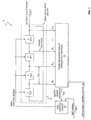
- Fig. 1 illustrates an exemplary frequency synthesizer circuit 10 according to one or more embodiments of this disclosure.
- the synthesizer circuit 10 comprises a ring oscillator circuit 12 that includes a plurality of delay stages 14, an oscillator control circuit 16, and a phase selection circuit 18.
- the synthesizer circuit 10 also is referred to as a phase-selectable ring oscillator circuit and its general operation is explained below.
- the frequency synthesizer circuit 10 is configured to generate an output clock signal having a desired frequency relationship to an input reference signal wherein that frequency relationship is determined by the phase selection sequence used to select the output clock signal phase fed back to the oscillator control circuit 16 at each successive cycle of the input reference signal. While those skilled in the art will recognize that basic ring oscillator circuits are known, this disclosure uses inventive phase selection generation to generate output clock signal frequencies having arbitrary frequency relationships to the reference signal frequencies. Moreover, the same selection sequence generation methods can be used to provide arbitrarily fine adjustment of the output frequency, e.g., ⁇ ⁇ 10 ppm, and, can be used to provide dynamic compensation for crystal oscillator variations arising from temperature, process, and voltage changes.
- the ring oscillator circuit 12 is configured to generate an output clock signal and to provide different phases of that output clock signal.
- the oscillator control circuit 16 is configured to control the oscillation frequency of the ring 12 based on comparing a selected phase of the output clock signal to the reference signal at each cycle of the reference signal.
- the phase selection circuit 18 is configured to generate a phase selection sequence corresponding to the desired frequency relationship between the reference signal and the output clock signal, and to feedback selected phases of the output clock signal to the oscillator control circuit 16 according to the phase selection sequence as defined by the input frequency control signal.
- the frequency of the output clock signal can be set relative to the input reference frequency by setting the phase selection step size via the frequency control signal, m .
- the phase selection circuit 18 selects a new phase of the output clock according to the value of m for feedback to the oscillator control circuit 16 at each cycle of the reference signal.
- the control circuit 16 generates a ring control signal that in an example is proportional to the phase difference between the feedback phase of the output clock signal and the reference signal.
- f FB is the multiplexed feedback signal generated by selecting different phases of the output clock signal over successive cycles of the input reference signal
- f REF is the frequency of the input reference signal
- N equals the number of delay stages 14
- m is the phase selection stepping size for cycle-to-cycle selection of output clock phases by phase selection circuit 18.
- a positive m indicates an advancing phase selection sequence that selects the next phase output feedback signal for comparison to the input reference signal by moving rightward by m delay stages 14 at each cycle of the reference signal.
- a negative value of m indicates a retreating phase selection sequence that moves leftward by m delay stages at each cycle of the reference signal.
- a retreating phase selection sequence results in f OUT ⁇ f REF
- an advancing phase selection sequence results in f OUT > f REF .
- phase selection circuit 18 uses a phase step size of 1, and moves leftward (earlier phases) as it selects a different phase of the output clock signal at each cycle of the reference signal.
- the phase selection sequence would be Phase N from stage 14- N , Phase N -1 from stage 14-( N- 1), Phase N- 2 from stage 14-( N- 2), Phase N- 3 from stage 14-( N- 3), and so on.
- the ring 12 appears to be running too fast, which causes control circuit 16 to slow the ring 12 down and thereby decrease its frequency.
- Setting m to -2 and stepping through the ring by two stages 14 per input reference signal cycle causes the feedback signal phase to appear too early by 2 x ⁇ .
- the converse relationship works with positive values of m. For example, if m equals +2, the feedback signal appears to be too late by an amount 2 x ⁇ at each cycle of the reference signal, which causes the control circuit 16 to increase the frequency of ring 12.
- the cycle-to-cycle phase selection step size m can be set to any effective value that is desired by generating an appropriate phase selection sequence.
- a sequence of phase selection step sizes can be generated to have any desired time-average value that can be a non-integer phase step size.
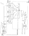
- Fig. 2 illustrates exemplary details for the circuit of Fig. 1 and provides a basis for discussing additional details of circuit 10 that complement the generation of non-uniform phase selection sequences to obtain arbitrary-valued phase stepping sizes.
- the phase selection circuit 18 is configured to generate non-uniform phase selection sequences to achieve such frequency relationships.
- non-uniform phase selection sequence connotes a phase selection sequence where the step size and or stepping direction may vary over successive cycles of the reference signal.
- an exemplary oscillator control circuit 16 is configured as a phase-locked loop (PLL) that generates a delay control signal as a function of the phase difference between the multiplexed feedback signal and the input reference signal.
- PLL-based phase detector configuration includes a phase comparator 20, a charge pump circuit 22, and a loop filter circuit 24 that in the illustration comprises a first-order RC filter.
- the charge pump circuit 22 sources current to or sinks current from the loop filter circuit 24, depending on whether the feedback signal phase leads or lags the reference signal phase.
- the amount of current sourced or sunk by charge pump circuit 22 is proportional to the magnitude of the phase difference and the loop filter circuit 24 time-averages the charge pump output to create a smoothly varying delay control signal that is applied to each delay stage 14 in the ring 12.
- the frequency synthesis circuit 10 described herein is its per-cycle comparison operation. That is, the multiplexed feedback signal's relative phase is changed at each cycle of the input reference signal and the resulting phase adjustments of the control circuit 16 thus occur at the input reference frequency rather than at some reduced fraction of the input frequency. Making ring control signal corrections at the input reference frequency allows favorable setting of the roll-off frequency of the filter circuit 24.
- the switch 28 moves clockwise or counterclockwise a defined number of switch positions at each cycle of the reference signal in dependence on the value of the selection signal input, labeled as SEL in the drawing.
- this disclosure provides a mechanism for creating essentially any effective value of m that is desired using modulator 34 or other "dithering" circuit to create the desired value m via non-uniform phase selection sequences. That is, modulator 34 provides a mechanism by which the phase selection circuit 18 can be configured to generate phase selection sequences having time-average values corresponding to fractional phase stepping sizes to thereby achieve arbitrary frequency relationships between f OUT and f REF , and to provide arbitrarily fine adjustment resolution of f OUT .
- ⁇ z F Q + e q 1 ⁇ z ⁇ 1 n , where e q is the quantization error.
- F may be restricted within the range [- Q /2 ... +Q /2] .
- the smallest possible quantization step is one. With the quantization error being sufficiently random, the spectral density of e q is then 1/12 f REF .
- modulator 34 is configured to generate the phase stepping modulation signal ⁇ ( z ) such that the frequency spectrum of the output phase noise is outside the frequency range of interest for the output clock signal. That effect can be accomplished by, for example, ensuring that the phase selection pattern generated by the m + ⁇ ( z ) does not have periodic variations that repeat within the frequency range of interest.
- the sequence of phase stepping values formed by m + ⁇ ( z ) can have essentially any desired time-average value.
- the value m can be generated as a sequence of 1s at the reference clock frequency, e.g., ⁇ 1, 1, 1, 1, ... ⁇ and modulator 34 can generate ⁇ ( z ) as an alternating sequence of -1 s and 0s, e.g., ⁇ 0, -1, 0, -1, ... ⁇ , such that the average value of m + ⁇ ( z ) is 0.5.
- phase selection sequence has a more random phase noise.
- this simple example is in no way limiting regarding the phase selection sequences used by this disclosure.
- the phase selection sequences can be generated such that the variations in the phase selection value appear more noise like, or at least avoid exhibiting periodicity within the frequency range of interest.
- modulator 34 can be configured to have a desired resolution, e.g., 16-bit, 20-bit, etc., such that the time-average value of the phase selection sequence output by counter 30 has a desired accuracy.
- 20-bit resolution in modulator 34 permits adjustment steps on the order of one-tenth ppm or less.
- the illustrated arrangement permits a system controller or other processor to set the value of F with an arbitrary level of precision to whatever real-valued number needed such that the combination of ⁇ ( z ) + m results in counter 30 outputting a phase selection sequence that yields the desired output frequency.
- circuit 10 can be modified to extend the range of f OUT to values less than 0.5 f REF or greater than 1.5 f REF .
- circuit 10 can be modified to include jitter control.
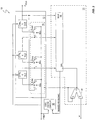
- Fig. 3 illustrates an exemplary configuration of circuit 10 wherein the ring 12 includes a jitter control circuit 40 comprising a plurality of switches arranged as one switch per phase output of the ring 12. Jitter control operation is explained below.
- the jitter circuit's switches are reset at each cycle of the reference signal on a per clock phase basis to null timing jitter every cycle. Resetting each switch causes the switch to move to "Position 1" slightly before the reference signal edge arrives and to return to "Position 2" shortly after each reference edge.
- each successive stage 14 in the ring 12 is clocked at the right successive phase time but without any edge jitter that might have been accumulated in any preceding stages 14.
- Jitter control circuit 40 can be clocked at the reference frequency using the SEL signal or using some other signal having the appropriate frequency.
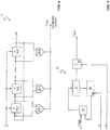
- Figs. 4 and 5 depict exemplary circuit arrangements for generating f OUT at multiples greater than 1.5 f REF ( Fig. 4 ) and less than 0.5 f REF ( Fig. 5 ).
- Fig. 4 illustrates the use of additional logic gates 44 (here, XOR gates) that provide two clock edges per delay stage 14 of ring 12.
- additional logic gates 44 here, XOR gates
- the final output frequency can take on essentially any desired value by adjusting the divide-by value of divider 46, which may itself be a fractional divider.
- Fig. 6 illustrates an example wherein a wireless communication device 50, e.g., a mobile terminal for use in a wireless communication network, includes at least one frequency synthesizer circuit 10 configured according to this disclosure.
- the illustrated device 50 comprises an antenna assembly that includes antenna 52 and switch/duplexer 54, and further comprises a receiver 56, a transmitter 58, a baseband signal processor 60, a system controller 62, one or more storage devices 64 (e.g., one or more memory circuits), a user interface 66 including, for example, a keypad, a display, a speaker, and a microphone, and an oscillator circuit 70 (e.g., a crystal oscillator).
- an oscillator circuit 70 e.g., a crystal oscillator
- oscillator circuit 70 is configured to run at one or more reference frequencies that serve as the time base for the clocked operations of processor circuits in the wireless device.
- the reference frequency time base often is chosen to complement the communication signal timing of the overall wireless system.
- oscillator circuit 70 can be configured for high accuracy, such circuits typically manifest enough frequency error to cause timing drift in device 50.
- One approach to compensating for frequency errors in the oscillator circuit has been to generate receiver and transmitter frequencies that are corrected for the measured frequency errors of circuit 70-device 50 may use one or more received signals to determine such frequency errors. While that conventional approach corrects the frequencies used in radio signal transmission and reception, it leaves uncorrected the underlying fundamental frequency signal output by circuit 70 and thus introduces timing drift into the operations of any circuit clocked by circuit 70.
- frequency synthesizer circuit 10 is configured to generate its clock output signal as a corrected version of the reference frequency output by circuit 70.
- the output clock signal from circuit 10 thus can be used as the system clock for baseband processor circuit 60, system controller 62, and any additional frequency synthesizers 68, which may or may not be configured according to this disclosure.
- an example exploits this disclosure's ability to make very fine frequency corrections, e.g., corrections in the ppm range, to null out measured errors in the reference frequency signal used by device 50 to time its overall communication signal processing operations.
- device 50 can be configured to determine the frequency error of oscillator circuit 70 using, for example, timing information derived from one or more received signals. While not shown explicitly, either baseband processor 60 and/or system controller 62 may receive a possibly divided down version of the output directly from oscillator circuit 70 and use that signal to measure timing errors. In any case, baseband processor 60 and/or system controller 62 determines the timing error of circuit 70 and generates m and F as needed to achieve the desired error nulling in the output clock signal from synthesizer circuit 10. That output clock signal thus provides an error-compensated fundamental reference frequency signal that is at the nominal reference frequency.
- baseband processor 60 and/or system controller 62 may dynamically adjust m and F as needed over time to dynamically track changing error in the oscillator circuit 70.
- the output frequency of oscillator circuit 70 may not be compensated for temperature and thus may exhibit a significant temperature coefficient.
- the values of m and/or F can be adjusted over time such that the error nulling tracks the changing error.
- error nulling may be made to track other environmental and process variations, such as supply voltage, etc.
- this disclosure offers obvious advantages to devices that require precision timing and synchronization, such as mobile terminals, but it can be applied to any type of device that uses clock signals of one sort or another.
- this disclosure is not limited by the foregoing discussion, or by the accompanying drawings. Indeed, this disclosure is limited only by the following claims and their reasonable equivalents.
Landscapes
- Stabilization Of Oscillater, Synchronisation, Frequency Synthesizers (AREA)
- Transceivers (AREA)
- Superheterodyne Receivers (AREA)
Abstract
Description
- The present invention generally relates to clock signal generation and particularly relates to synthesizing desired clock frequencies.
- Frequency synthesis can be defined broadly as the act of generating a desired frequency from one or more reference frequencies. For example, frequency synthesis may be used to create one or more output frequencies using a single reference frequency. Other forms of frequency synthesis derived desired output frequencies based on the interaction of two or more reference signals, each at a different frequency.
- As might be imagined, frequency synthesis in its various forms finds widespread use across a variety of system and device types. One exemplary use of frequency synthesis is the creation of one or more system clock signals from a single reference frequency signal. Synthesizing the system clock signals from the same reference frequency ensures that all clock timing relates back to the same base frequency. Such synchronization can be important in sampled data systems wherein the process of converting analog signals into digitized samples must be carried out in synchronization with a microprocessor clock or other system clock.
- The use of multiple frequencies synchronized to the same baseline reference frequency also is important in many types of communication systems, including wired (electrical and optical), and wireless communication systems. For example, mobile terminals typically use multiple frequencies in their operations, including different frequencies for receive/transmit signal mixing, filtering, down-conversion, signal digitization, and baseband digital processing. Because such operations typically must be performed in synchronization with a baseline system timing, such mobile terminals typically have a reference clock running at a baseline frequency, and typically employ one or more frequency synthesizers to generate one or more additional clock signals having desired frequency relationships to the reference clock signal.
- Of course, such aspects and applications of frequency synthesis are well known to those skilled in the art, and certain forms of frequency synthesis can be implemented using relatively straightforward circuits, such as the use of simple multipliers and/or dividers to achieve synthesized frequencies that are integer multiples or factors of the reference frequency, e.g., 2x, 3x, 1/2x, 1/4x. However, synthesis becomes more complicated when the desired frequency relationship between the reference and output signals has a fractional component.
- This disclosure comprises a method and apparatus to generate a clock signal with an essentially arbitrary frequency relationship to a reference signal. In particular, this disclosure provides an exemplary frequency synthesis method based on using multiple output phases of a ring oscillator circuit to achieve arbitrarily small frequency adjustment steps for the output clock signal, thereby making possible the accurate synthesis of arbitrarily valued frequencies relative to a reference frequency. As such, this disclosure provides a basis for very precisely setting the frequency of a clock signal. For example, this disclosure may be used to apply frequency corrections in the order of just a few parts-per-million (ppm) such that small errors in a reference frequency signal can be nullified.
- Broadly, the present invention comprises a frequency synthesis circuit including a selectable-phase ring oscillator circuit that generates an output clock signal at a desired frequency relative to an input reference signal frequency. The output frequency depends on the phase selection sequence used to drive the ring oscillator circuit during its operation, and the exemplary circuit includes a phase selection generator that can generate phase selection sequences having effective fractional or non-fractional phase selection step sizes as needed to achieve the desired frequency relationship.
- Aspects of the invention are presented in the independent claims, and embodiments thereof are presented in the dependent claims.
- Thus, in an example, this disclosure comprises a method of generating an output clock signal having a desired frequency relationship to a reference signal. This exemplary method comprises generating the output clock signal in a ring oscillator circuit that provides different phases of the output clock signal, controlling an oscillation frequency of the ring oscillator circuit based on selecting a phase of the output clock signal at each cycle of the reference signal and comparing the selected phase of the output clock signal to the reference signal, and generating a phase selection sequence for selecting phases of the output clock signal to effect the desired frequency relationship.
- In another example, this disclosure comprises a frequency synthesizer circuit. Thus, the exemplary circuit comprises a ring oscillator circuit configured to generate an output clock signal and to provide different phases of the output clock signal, an oscillator control circuit configured to control an oscillation frequency of the ring oscillator circuit based on comparing a selected phase of the output clock signal to a reference signal at each cycle of the reference signal, and a phase selection circuit configured to generate a phase selection sequence corresponding to a desired frequency relationship between the reference signal and the output clock signal, and to feedback selected phases of the output clock signal to the oscillator control circuit according to the phase selection sequence.
- In accordance with one or more examples of this disclosure, an exemplary phase selection circuit is configured to control the frequency of the output clock signal by selecting a different phase of the output clock signal for feedback to the oscillator control circuit at each cycle of the reference signal according to a phase selection sequence. The phase selection circuit may be configured to generate phase selection sequences having sequence averages corresponding to non-integer (fractional) phase selection step sizes in dependence on a frequency relationship between a desired frequency of the output clock signal and a frequency of the reference signal. That is, this disclosure enables the exemplary frequency synthesizer circuit to generate essentially any desired frequency relative to a reference signal frequency by generating phase selection sequences having time-averaged values corresponding to real-valued phase selection step sizes of arbitrarily fine resolution.
- Of course, this disclosure is not limited by the above summary information. Those skilled in the art will recognize other features and advantages upon reading the following discussion and upon viewing the accompanying figures.
-
-
Fig. 1 is a diagram of an exemplary frequency synthesizer circuit according to this disclosure. -
Fig. 2 is a diagram of exemplary details for the circuit ofFig. 1 . -
Fig. 3 is a diagram of exemplary jitter control circuit details. -
Figs. 4 and 5 are diagrams of exemplary circuits to extend output frequency ranges. -
Fig. 6 is a diagram of an exemplary wireless communication terminal that includes one or more frequency synthesizers configured according to this disclosure. - Numerous references appear throughout the following discussion regarding the configuration and use of frequency synthesizers according to this disclosure in the context of wireless communication devices and/or systems, such as cellular radiotelephones, Portable Digital Assistants (PDAs), laptop/palmtop computers, etc. Indeed, one or more of the accompanying figures illustrate a wireless communication terminal that includes one or more such frequency synthesizers. However, it should be understood that this disclosure has broad applicability to essentially any type of electronic device or system wherein flexible and precise frequency generation is useful.
- With the above in mind,
Fig. 1 illustrates an exemplaryfrequency synthesizer circuit 10 according to one or more embodiments of this disclosure. As illustrated, thesynthesizer circuit 10 comprises aring oscillator circuit 12 that includes a plurality ofdelay stages 14, anoscillator control circuit 16, and aphase selection circuit 18. Thesynthesizer circuit 10 also is referred to as a phase-selectable ring oscillator circuit and its general operation is explained below. - Broadly, the
frequency synthesizer circuit 10 is configured to generate an output clock signal having a desired frequency relationship to an input reference signal wherein that frequency relationship is determined by the phase selection sequence used to select the output clock signal phase fed back to theoscillator control circuit 16 at each successive cycle of the input reference signal. While those skilled in the art will recognize that basic ring oscillator circuits are known, this disclosure uses inventive phase selection generation to generate output clock signal frequencies having arbitrary frequency relationships to the reference signal frequencies. Moreover, the same selection sequence generation methods can be used to provide arbitrarily fine adjustment of the output frequency, e.g., < ± 10 ppm, and, can be used to provide dynamic compensation for crystal oscillator variations arising from temperature, process, and voltage changes. - In more detail, the
ring oscillator circuit 12 is configured to generate an output clock signal and to provide different phases of that output clock signal. In turn, theoscillator control circuit 16 is configured to control the oscillation frequency of thering 12 based on comparing a selected phase of the output clock signal to the reference signal at each cycle of the reference signal. Thephase selection circuit 18 is configured to generate a phase selection sequence corresponding to the desired frequency relationship between the reference signal and the output clock signal, and to feedback selected phases of the output clock signal to theoscillator control circuit 16 according to the phase selection sequence as defined by the input frequency control signal. - With the above exemplary configuration, the frequency of the output clock signal can be set relative to the input reference frequency by setting the phase selection step size via the frequency control signal, m. More specifically, the
phase selection circuit 18 selects a new phase of the output clock according to the value of m for feedback to theoscillator control circuit 16 at each cycle of the reference signal. In turn, thecontrol circuit 16 generates a ring control signal that in an example is proportional to the phase difference between the feedback phase of the output clock signal and the reference signal. The control signal generated byoscillator control circuit 16 varies the oscillation frequency of thering 12, and its basic control function is given as,

- Where is the unit delay of each
stage 14 in thering 12, fFB is the multiplexed feedback signal generated by selecting different phases of the output clock signal over successive cycles of the input reference signal, fREF is the frequency of the input reference signal, N equals the number ofdelay stages 14, and m is the phase selection stepping size for cycle-to-cycle selection of output clock phases byphase selection circuit 18. - In turn, the frequency fOUT of the output clock signal is given as,


- In the illustrations of
Figs. 1 and2 , a positive m indicates an advancing phase selection sequence that selects the next phase output feedback signal for comparison to the input reference signal by moving rightward bym delay stages 14 at each cycle of the reference signal. Conversely, a negative value of m indicates a retreating phase selection sequence that moves leftward by m delay stages at each cycle of the reference signal. A retreating phase selection sequence results in fOUT < fREF, while an advancing phase selection sequence results in fOUT > fREF. (The trivial case of m = 0, i.e., no cycle-to-cycle phase stepping, results in fOUT = fREF.) Also, note that the selection sequence wraps around from the beginning to end of thering 12 or vice versa, depending on the selection direction. - To better understand the above relationships, assume m equals -1, meaning that the
phase selection circuit 18 uses a phase step size of 1, and moves leftward (earlier phases) as it selects a different phase of the output clock signal at each cycle of the reference signal. Thus, the phase selection sequence would be Phase N from stage 14-N, Phase N-1 from stage 14-(N-1), Phase N-2 from stage 14-(N-2), Phase N-3 from stage 14-(N-3), and so on. By advancing the feedback signal by onestage 14 at each comparison cycle of the input reference signal, the feedback signal's phase is early by an amount m x Δφ (here, m = -1). Thus, from the perspective of theoscillator control circuit 16, thering 12 appears to be running too fast, which causescontrol circuit 16 to slow thering 12 down and thereby decrease its frequency. Setting m to -2 and stepping through the ring by twostages 14 per input reference signal cycle causes the feedback signal phase to appear too early by 2 x Δφ. Of course, the converse relationship works with positive values of m. For example, if m equals +2, the feedback signal appears to be too late by an amount 2 x Δφ at each cycle of the reference signal, which causes thecontrol circuit 16 to increase the frequency ofring 12. - One of the advantages of this disclosure is that the cycle-to-cycle phase selection step size m can be set to any effective value that is desired by generating an appropriate phase selection sequence. In other words, a sequence of phase selection step sizes can be generated to have any desired time-average value that can be a non-integer phase step size. As a simple example, the phase selection sequence is m = {1, 1, 1, 0, 1, 1, 1, 0, 1, 1, 1, 0, ...}. That sequence would cause the
phase selection circuit 18 to advance rightward to the next delay stage's phase output three out of every four successive cycles of the reference signal. The effect of holding the currently selected phase over every fourth cycle of the reference signal is to have an effectively non-integer phase stepping size of m = 0.75. -
Fig. 2 illustrates exemplary details for the circuit ofFig. 1 and provides a basis for discussing additional details ofcircuit 10 that complement the generation of non-uniform phase selection sequences to obtain arbitrary-valued phase stepping sizes. Thus, the above discussion is expanded to consider frequency synthesis situations wherein the desired frequency relationship between the reference signal and the output clock signal cannot be achieved by integer phase step sizes. In one or more examples, thephase selection circuit 18 is configured to generate non-uniform phase selection sequences to achieve such frequency relationships. As used herein, the term "non-uniform" phase selection sequence connotes a phase selection sequence where the step size and or stepping direction may vary over successive cycles of the reference signal. - Turning to the additional diagram details, one sees that an exemplary
oscillator control circuit 16 is configured as a phase-locked loop (PLL) that generates a delay control signal as a function of the phase difference between the multiplexed feedback signal and the input reference signal. An exemplary PLL-based phase detector configuration includes aphase comparator 20, acharge pump circuit 22, and aloop filter circuit 24 that in the illustration comprises a first-order RC filter. At each cycle of the input reference signal, thecharge pump circuit 22 sources current to or sinks current from theloop filter circuit 24, depending on whether the feedback signal phase leads or lags the reference signal phase. The amount of current sourced or sunk bycharge pump circuit 22 is proportional to the magnitude of the phase difference and theloop filter circuit 24 time-averages the charge pump output to create a smoothly varying delay control signal that is applied to eachdelay stage 14 in thering 12. - Indeed, one of the many advantages provided by the
frequency synthesis circuit 10 described herein is its per-cycle comparison operation. That is, the multiplexed feedback signal's relative phase is changed at each cycle of the input reference signal and the resulting phase adjustments of thecontrol circuit 16 thus occur at the input reference frequency rather than at some reduced fraction of the input frequency. Making ring control signal corrections at the input reference frequency allows favorable setting of the roll-off frequency of thefilter circuit 24. - In highlighting other illustrated details, note that
phase selection circuit 18 comprises amultiplexer circuit 26 including acontrollable switch 28, a modulo-N accumulator (Y=(A+B) mod N) 30, a summingcircuit 32, and asequence modulator 34 that comprises a modulo Q delta-sigma (ΔΣ) modulator in an example. Theswitch 28 moves clockwise or counterclockwise a defined number of switch positions at each cycle of the reference signal in dependence on the value of the selection signal input, labeled as SEL in the drawing. - In elaborating on the functionality provided by the depicted circuit arrangement, the discussion returns to Eq. (4) given above in the context of
modulator 34. Eq. (4) illustrated that fOUT is a function of fREF and m, i.e., fOUT = f(fREF, m). In looking at that relationship, one sees that an arbitrary relationship can be achieved so long as the value of m can be set to an arbitrary value. For example, if m can be set to essentially any desired value within the range of 0.5 fREF < m < 1.5 fREF, then thefrequency synthesizer circuit 10 can be used to make arbitrarily small corrections to fREF. As will be discussed herein, such operation has particular advantages in correcting even very small frequency errors in a reference clock circuit to prevent such errors from causing timing drift in one or more clocked circuits that depend on the reference clock. - In these and other applications, this disclosure provides a mechanism for creating essentially any effective value of m that is desired using
modulator 34 or other "dithering" circuit to create the desired value m via non-uniform phase selection sequences. That is,modulator 34 provides a mechanism by which thephase selection circuit 18 can be configured to generate phase selection sequences having time-average values corresponding to fractional phase stepping sizes to thereby achieve arbitrary frequency relationships between fOUT and fREF, and to provide arbitrarily fine adjustment resolution of fOUT. - With the addition of
modulator 34 andsummer 32, the output frequency fOUT can be expressed as,

modulator 34 with a generic noise transfer function (i.e., a cascade of integrators), a modulator modulus of Q, and a fractional input signal value F. Generally, F may be restricted within the range [-Q/2 ... +Q/2]. - Because of the digital nature of the quantizer in the delta-sigma modulator implementation, the smallest possible quantization step is one. With the quantization error being sufficiently random, the spectral density of eq is then 1/12fREF . The integral of the quantization noise related frequency fluctuation leads to the single-sided power spectral density of the phase fluctuations of the output clock signal, which can be expressed as,

- The above result can be multiplied by the magnitude of the loop phase transfer function of the
control circuit 16 andring circuit 12, |H(s)|2, to obtain the measurable output phase noise spectrum of the output clock signal. In accordance with one or more embodiments of this disclosure,modulator 34 is configured to generate the phase stepping modulation signal Δ(z) such that the frequency spectrum of the output phase noise is outside the frequency range of interest for the output clock signal. That effect can be accomplished by, for example, ensuring that the phase selection pattern generated by the m + Δ(z) does not have periodic variations that repeat within the frequency range of interest. - In general, one should note that the sequence of phase stepping values formed by m + Δ(z) can have essentially any desired time-average value. For example, assuming that the desired frequency relationship between fREF and fOUT required an effective phase step size of 0.5. The value m can be generated as a sequence of 1s at the reference clock frequency, e.g., {1, 1, 1, 1, ...} and
modulator 34 can generate Δ(z) as an alternating sequence of -1 s and 0s, e.g., {0, -1, 0, -1, ...}, such that the average value of m + Δ(z) is 0.5. Of course, as just noted above, a more preferred averaging scheme might be implemented such that the phase selection sequence has a more random phase noise. As such, a better sequence might be m + Δ(z) = {1, 1, 1, 0, 1, 1, 0, 0, 1, 0, 0, 0, ...}. Of course, those skilled in the art will appreciate that this simple example is in no way limiting regarding the phase selection sequences used by this disclosure. In general, the phase selection sequences can be generated such that the variations in the phase selection value appear more noise like, or at least avoid exhibiting periodicity within the frequency range of interest. - In general,
modulator 34 can be configured to have a desired resolution, e.g., 16-bit, 20-bit, etc., such that the time-average value of the phase selection sequence output bycounter 30 has a desired accuracy. For example, 20-bit resolution inmodulator 34 permits adjustment steps on the order of one-tenth ppm or less. In other words, the illustrated arrangement permits a system controller or other processor to set the value of F with an arbitrary level of precision to whatever real-valued number needed such that the combination of Δ(z) + m results incounter 30 outputting a phase selection sequence that yields the desired output frequency. With this configuration, then, the frequency of the output clock signal can be expressed as,
- As a basis for a simple example, assume that fREF = 26.00 MHz, the desired fREF = 30.72 MHz (i.e., fREF = fREF x (1+59/325). Then, depending on the number of
stages 14 inring 12, the necessary parameters and quantizer level choices given in Table 1 below.Table 1. Exemplary Parameter and Quantizer Values. N m F Q Δ 4 1 147 325 {0,1} 8 3 -31 325 {-1,0,1} 16 6 -62 325 {-1,0,1} 32 12 -124 325 {-1,0,1} modulator 34, the cycle-to-cycle phase step sizes are in the range of m+Δ(z) = {2,3,4}. In the locked condition, eachdelay stage 14 has a delay of τ = 1/(2 x 8 x 30.72 MHz) = 2.03 ns. - Of course, this disclosure is not limited to the circuit arrangements illustrated thus far. For example,
circuit 10 can be modified to extend the range of fOUT to values less than 0.5 fREF or greater than 1.5 fREF. Additionally or alternatively,circuit 10 can be modified to include jitter control.Fig. 3 illustrates an exemplary configuration ofcircuit 10 wherein thering 12 includes a jitter control circuit 40 comprising a plurality of switches arranged as one switch per phase output of thering 12. Jitter control operation is explained below. - In the locked condition of
control circuit 16, signal edges of the reference signal align with corresponding edges in the multiplexed feedback signal provided byphase selection circuit 18. When in the locked condition, alignment differences between edges in the reference signal and in the feedback signal occur because of timing jitter. Edges in the reference signal can be used in the locked condition to reset thering 12 at each cycle of the reference signal to remove accumulated timing jitter. - In more detail, when the
control circuit 16 is in the locked condition, the jitter circuit's switches are reset at each cycle of the reference signal on a per clock phase basis to null timing jitter every cycle. Resetting each switch causes the switch to move to "Position 1" slightly before the reference signal edge arrives and to return to "Position 2" shortly after each reference edge. Thus, eachsuccessive stage 14 in thering 12 is clocked at the right successive phase time but without any edge jitter that might have been accumulated in any precedingstages 14. Jitter control circuit 40 can be clocked at the reference frequency using the SEL signal or using some other signal having the appropriate frequency. -
Figs. 4 and 5 depict exemplary circuit arrangements for generating fOUT at multiples greater than 1.5 fREF (Fig. 4 ) and less than 0.5 fREF (Fig. 5 ). Those skilled in the art will appreciate that other circuit arrangements can be used to achieve the same effects. In any case,Fig. 4 illustrates the use of additional logic gates 44 (here, XOR gates) that provide two clock edges perdelay stage 14 ofring 12. With this configuration, the signal frequency at the combined output will be N times higher than the fundamental reference frequency and thus can be expressed with respect to Eq. (8) as,
- With regard to
Fig. 5 , those skilled in the art will appreciate that the final output frequency can take on essentially any desired value by adjusting the divide-by value ofdivider 46, which may itself be a fractional divider. - Any of the above embodiments may be employed in a wide variety of systems.
Fig. 6 illustrates an example wherein awireless communication device 50, e.g., a mobile terminal for use in a wireless communication network, includes at least onefrequency synthesizer circuit 10 configured according to this disclosure. The illustrateddevice 50 comprises an antenna assembly that includesantenna 52 and switch/duplexer 54, and further comprises areceiver 56, atransmitter 58, abaseband signal processor 60, asystem controller 62, one or more storage devices 64 (e.g., one or more memory circuits), auser interface 66 including, for example, a keypad, a display, a speaker, and a microphone, and an oscillator circuit 70 (e.g., a crystal oscillator). - Commonly,
oscillator circuit 70 is configured to run at one or more reference frequencies that serve as the time base for the clocked operations of processor circuits in the wireless device. In wireless communication devices in particular, the reference frequency time base often is chosen to complement the communication signal timing of the overall wireless system. - While
oscillator circuit 70 can be configured for high accuracy, such circuits typically manifest enough frequency error to cause timing drift indevice 50. One approach to compensating for frequency errors in the oscillator circuit has been to generate receiver and transmitter frequencies that are corrected for the measured frequency errors of circuit 70-device 50 may use one or more received signals to determine such frequency errors. While that conventional approach corrects the frequencies used in radio signal transmission and reception, it leaves uncorrected the underlying fundamental frequency signal output bycircuit 70 and thus introduces timing drift into the operations of any circuit clocked bycircuit 70. - According to an example of this disclosure,
frequency synthesizer circuit 10 is configured to generate its clock output signal as a corrected version of the reference frequency output bycircuit 70. The output clock signal fromcircuit 10 thus can be used as the system clock forbaseband processor circuit 60,system controller 62, and anyadditional frequency synthesizers 68, which may or may not be configured according to this disclosure. In other words, an example exploits this disclosure's ability to make very fine frequency corrections, e.g., corrections in the ppm range, to null out measured errors in the reference frequency signal used bydevice 50 to time its overall communication signal processing operations. - As such,
device 50 can be configured to determine the frequency error ofoscillator circuit 70 using, for example, timing information derived from one or more received signals. While not shown explicitly, eitherbaseband processor 60 and/orsystem controller 62 may receive a possibly divided down version of the output directly fromoscillator circuit 70 and use that signal to measure timing errors. In any case,baseband processor 60 and/orsystem controller 62 determines the timing error ofcircuit 70 and generates m and F as needed to achieve the desired error nulling in the output clock signal fromsynthesizer circuit 10. That output clock signal thus provides an error-compensated fundamental reference frequency signal that is at the nominal reference frequency. - Further,
baseband processor 60 and/orsystem controller 62 may dynamically adjust m and F as needed over time to dynamically track changing error in theoscillator circuit 70. As one example, the output frequency ofoscillator circuit 70 may not be compensated for temperature and thus may exhibit a significant temperature coefficient. By observing the output fromoscillator circuit 70, or by tracking temperature changes and using assumed or calibrated temperature coefficient data foroscillator circuit 70, the values of m and/or F can be adjusted over time such that the error nulling tracks the changing error. Of course, those skilled in the art will appreciate that with the fine adjustment afforded by this disclosure, error nulling may be made to track other environmental and process variations, such as supply voltage, etc. - In any case, this disclosure offers obvious advantages to devices that require precision timing and synchronization, such as mobile terminals, but it can be applied to any type of device that uses clock signals of one sort or another. As such, this disclosure is not limited by the foregoing discussion, or by the accompanying drawings. Indeed, this disclosure is limited only by the following claims and their reasonable equivalents.
-
- 1. A method of generating an output clock signal having a desired frequency relationship to a reference signal, the method comprising:
- generating the output clock signal in a ring oscillator circuit that provides different phases of the output clock signal;
- controlling an oscillation frequency of the ring oscillator circuit based on selecting a phase of the output clock signal at each cycle of the reference signal and comparing the selected phase of the output clock signal to the reference signal; and
- generating a phase selection sequence for selecting phases of the output clock signal to effect the desired frequency relationship.
- 2. The method of
claim 1, wherein generating a phase selection sequence for selecting phases of the output clock signal to effect the desired frequency relationship comprises generating a uniform or a non-uniform phase selection sequence as needed to effect the desired frequency relationship. - 3. The method of
claim 1, wherein generating a phase selection sequence for selecting phases of the output clock signal to effect the desired frequency relationship comprises generating a uniform phase selection sequence having a fixed phase selection step size and a fixed phase selection direction. - 4. The method of
claim 1, wherein generating a phase selection sequence for selecting phases of the output clock signal to effect the desired frequency relationship comprises generating a non-uniform phase selection sequence having at least one of a variable phase selection step size and a variable phase selection direction. - 5. The method of
claim 1, wherein the oscillation frequency of the ring oscillator circuit and, hence, of the output clock signal, is a function of a phase selection step size used over successive cycles of the reference signal to select the phases of output clock signal for comparison to the reference signal, and wherein generating a phase selection sequence for selecting phases of the output clock signal to effect the desired frequency relationship comprises calculating a real-valued effective step size needed to achieve the desired frequency relationship and generating a sequence of integer step sizes having a time-average value substantially equal to the effective step size. - 6. The method of claim 5, further comprising generating the sequence of integer step sizes to achieve a desired power spectral density, such that a majority of sequence noise power falls outside a frequency band around the oscillation frequency.
- 7. The method of
claim 1, wherein generating a phase selection sequence for selecting phases of the output clock signal to effect the desired frequency relationship comprises applying a phase selection step size corresponding to the desired frequency relationship as an input to a delta-sigma modulator, and driving a phase selection counter based on an output of the delta-sigma modulator. - 8. The method of
claim 1, wherein controlling an oscillation frequency of the ring oscillator circuit based on selecting a phase of the output clock signal at each cycle of the reference signal and comparing the selected phase of the output clock signal to the reference signal comprises generating a delay control signal operative to vary an overall delay of the ring oscillator circuit based on a phase difference at each cycle of the reference signal between the reference signal and the selected phase of the output clock signal. - 9. The method of
claim 1, wherein the reference signal comprises an oscillator output signal and wherein the method further comprises determining a frequency error of the oscillator output signal relative to a nominal oscillation frequency and generating the phase sequence such that the clock output signal is at the nominal oscillation frequency. - 10. The method of
claim 1, wherein the reference signal comprises an oscillator output signal, and wherein the method further comprises receiving at a communication device one or more signals from a remote transmitter, determining a frequency error of the oscillator output signal based on the one or more signals, and generating the phase selection sequence to null the frequency error from the output clock signal. - 11. The method of
claim 10, further comprising using the output clock signal rather than the oscillator output signal as a system clock signal for clocking one or more clocked circuits in the communication device such that the frequency error of the oscillator output signal does not cause timing drift between the clocked circuits in the communication device and the remote transmitter. - 12. A frequency synthesizer circuit comprising:
- a ring oscillator circuit configured to generate an output clock signal and to provide different phases of the output clock signal;
- an oscillator control circuit configured to control an oscillation frequency of the ring oscillator circuit based on comparing a selected phase of the output clock signal to a reference signal at each cycle of the reference signal; and
- a phase selection circuit configured to generate a phase selection sequence corresponding to a desired frequency relationship between the reference signal and the output clock signal, and to feedback selected phases of the output clock signal to the oscillator control circuit according to the phase selection sequence.
- 13. The frequency synthesizer circuit of
claim 12, wherein the phase selection circuit is configured to generate a uniform or a non-uniform phase selection sequence as needed to effect the desired frequency relationship. - 14. The frequency synthesizer circuit of
claim 12, wherein the phase selection circuit is configured to generate uniform phase selection sequences based on fixed phase selection step sizes and fixed phase selection directions. - 15. The frequency synthesizer circuit of
claim 12, wherein the phase selection circuit is configured to generate non-uniform phase selection sequences by varying at least one of a phase selection step size and a phase selection direction over successive cycles of the reference signal. - 16. The frequency synthesizer circuit of
claim 12, wherein the oscillation frequency of the ring oscillator circuit and, hence, of the output clock signal, is a function of a phase selection step size used over successive cycles of the reference signal to select the phases of output clock signal for comparison to the reference signal, and wherein the phase selection circuit is configured to generate a phase selection sequence for selecting phases of the output clock signal to effect the desired frequency relationship by calculating a real-valued effective step size needed to achieve the desired frequency relationship and generating a sequence of integer step sizes having a time-average value substantially equal to the effective step size. - 17. The frequency synthesizer circuit of
claim 16, wherein the phase selection circuit is configured to generate the sequence of integer step sizes based on a desired power spectral density, such that a majority of sequence noise power falls outside a frequency band around the oscillation frequency of the ring oscillator circuit. - 18. The frequency synthesizer circuit of
claim 12, wherein phase selection circuit includes a delta-sigma converter configured to receive a phase selection step size corresponding to the desired frequency relationship and to output a corresponding sequence of phase selection values that are used to select phases of the output clock signal. - 19. The frequency synthesizer circuit of
claim 12, wherein the oscillator control circuit comprises a phase detector circuit configured to generate a delay control signal based on a phase difference at each cycle of the reference signal between the reference signal and the selected phase of the output clock signal, and wherein the delay control signal is operative to vary an overall delay of the ring oscillator circuit. - 20. A frequency synthesizer circuit comprising:
- a ring oscillator circuit configured to generate an output clock signal and comprising a plurality of successive delay stages, each stage offering a different phase of the output clock signal;
- an oscillator control circuit configured to control a frequency of the clock output signal based on comparing a selected phase of the output clock signal at each cycle of an input reference signal; and
- a phase selection circuit configured to control the frequency of the output clock signal by selecting a different phase of the output clock signal for feedback to the oscillator control circuit at each cycle of the reference signal according to a phase selection sequence, said phase selection circuit configured to generate phase selection sequences having sequence averages corresponding to non-integer phase selection step sizes in dependence on a frequency relationship between a desired frequency of the output clock signal and a frequency of the reference signal.
- 21. A frequency synthesizer circuit comprising a selectable-phase ring oscillator circuit configured to generate an output clock signal at an output clock frequency having a frequency relationship to a reference signal frequency that depends on a phase selection sequence used to drive the selectable-phase ring oscillator, said selectable-phase ring oscillator circuit including a phase selection circuit configured to generate phase selection sequences having fractional or non-fractional effective phase selection step sizes as needed to effect desired frequency relationships.
- 22. A wireless communication terminal comprising:
- a transceiver circuit configured to send and receive wireless signals;
- one or more clocked processor circuits configured to control the transceiver circuits; an oscillator circuit configured to generate a reference signal;
- a frequency synthesizer circuit configured to generate an output clock signal having a desired frequency relationship to the reference signal for clocking the one or more clocked processor circuits;
- said frequency synthesizer circuit comprising a selectable-phase feedback ring oscillator circuit configured to generate the output clock signal based on fractional or non-fractional phase steps sizes as needed to obtain the desired frequency relationship between the reference signal and the output clock signal.
- 23. The terminal of
claim 22, wherein the frequency synthesizer circuit is configured to generate one or more reference frequency signals from the output clock signal for use in transceiver operations.
Claims (3)
- A selectable-phase ring oscillator circuit comprising a plurality of successive delay stages, each stage offering a different phase of the output clock signal and configured to generate an output clock signal at an output frequency having a relation to a reference frequency of an input reference signal, wherein selectable-phase ring oscillator circuit is configured such that the output frequency depends on a phase selection sequence used to drive the ring oscillator circuit during its operation, and the selectable-phase ring oscillator circuit includes a phase selection generator configured to generate phase selection sequences having effective fractional or non-fractional phase selection step sizes as needed to achieve the relationship between the output frequency and the reference frequency.
- A frequency synthesizer circuit comprising:a selectable-phase ring oscillator circuit according to claim 1;an oscillator control circuit configured to control a frequency of the clock output signal based on comparing a selected phase of the output clock signal at each cycle of an input reference signal; anda phase selection circuit configured to control the frequency of the output clock signal by selecting a different phase of the output clock signal for feedback to the oscillator control circuit at each cycle of the reference signal according to a phase selection sequence,said phase selection circuit configured to generate phase selection sequences having sequence averages corresponding to non-integer phase selection step sizes in dependence on a frequency relationship between a desired frequency of the output clock signal and a frequency of the reference signal.
- A wireless communication terminal comprising:a transceiver circuit configured to send and receive wireless signals;one or more clocked processor circuits configured to control the transceiver circuits; an oscillator circuit configured to generate a reference signal; anda frequency synthesizer circuit according to claim 2 configured to generate an output clock signal having a desired frequency relationship to the reference signal for clocking the one or more clocked processor circuits.
Applications Claiming Priority (3)
| Application Number | Priority Date | Filing Date | Title |
|---|---|---|---|
| US10/794,830 US7356312B2 (en) | 2004-03-05 | 2004-03-05 | Fractional frequency synthesizer |
| PCT/EP2005/001616 WO2006045346A1 (en) | 2004-03-05 | 2005-02-17 | Fractional frequency synthesizer |
| EP05849342.0A EP1721388B1 (en) | 2004-03-05 | 2005-02-17 | Fractional frequency synthesizer |
Related Parent Applications (2)
| Application Number | Title | Priority Date | Filing Date |
|---|---|---|---|
| EP05849342.0A Division EP1721388B1 (en) | 2004-03-05 | 2005-02-17 | Fractional frequency synthesizer |
| EP05849342.0A Division-Into EP1721388B1 (en) | 2004-03-05 | 2005-02-17 | Fractional frequency synthesizer |
Publications (2)
| Publication Number | Publication Date |
|---|---|
| EP3208943A1 true EP3208943A1 (en) | 2017-08-23 |
| EP3208943B1 EP3208943B1 (en) | 2019-10-23 |
Family
ID=34912360
Family Applications (2)
| Application Number | Title | Priority Date | Filing Date |
|---|---|---|---|
| EP05849342.0A Active EP1721388B1 (en) | 2004-03-05 | 2005-02-17 | Fractional frequency synthesizer |
| EP17163737.4A Active EP3208943B1 (en) | 2004-03-05 | 2005-02-17 | Fractional frequency synthesizer |
Family Applications Before (1)
| Application Number | Title | Priority Date | Filing Date |
|---|---|---|---|
| EP05849342.0A Active EP1721388B1 (en) | 2004-03-05 | 2005-02-17 | Fractional frequency synthesizer |
Country Status (4)
| Country | Link |
|---|---|
| US (1) | US7356312B2 (en) |
| EP (2) | EP1721388B1 (en) |
| JP (1) | JP4648380B2 (en) |
| WO (1) | WO2006045346A1 (en) |
Families Citing this family (12)
| Publication number | Priority date | Publication date | Assignee | Title |
|---|---|---|---|---|
| US7706992B2 (en) | 2005-02-23 | 2010-04-27 | Digital Intelligence, L.L.C. | System and method for signal decomposition, analysis and reconstruction |
| US7605665B2 (en) * | 2007-05-25 | 2009-10-20 | Broadcom Corporation | Fractional-N phase locked loop |
| US20090088194A1 (en) | 2007-09-27 | 2009-04-02 | Telefonaktiebolaget Lm Ericsson (Publ) | Single Multi-Mode Clock Source for Wireless Devices |
| US7911247B2 (en) * | 2008-02-26 | 2011-03-22 | Qualcomm Incorporated | Delta-sigma modulator clock dithering in a fractional-N phase-locked loop |
| US8085097B2 (en) * | 2008-05-06 | 2011-12-27 | Hittite Microwave Corporation | Integrated ramp, sweep fractional frequency synthesizer on an integrated circuit chip |
| US8350628B1 (en) | 2011-02-15 | 2013-01-08 | Western Digital Technologies, Inc. | Gate speed regulator dithering ring oscillator to match critical path circuit |
| US8818282B2 (en) * | 2011-08-11 | 2014-08-26 | Qualcomm Incorporated | Clock sharing between cores on an integrated circuit |
| JP5792557B2 (en) * | 2011-08-16 | 2015-10-14 | 株式会社メガチップス | Frequency synthesizer |
| EP2954621B1 (en) | 2013-02-07 | 2018-05-16 | Widex A/S | A transceiver for a hearing aid and a method for operating such a transceiver |
| US9225348B2 (en) * | 2014-01-10 | 2015-12-29 | International Business Machines Corporation | Prediction based digital control for fractional-N PLLs |
| US11602311B2 (en) | 2019-01-29 | 2023-03-14 | Murata Vios, Inc. | Pulse oximetry system |
| EP3954044A1 (en) * | 2019-04-11 | 2022-02-16 | Telefonaktiebolaget LM Ericsson (publ) | Frequency detector for measuring and tuning frequency of controlled oscillator |
Citations (4)
| Publication number | Priority date | Publication date | Assignee | Title |
|---|---|---|---|---|
| US5889436A (en) * | 1996-11-01 | 1999-03-30 | National Semiconductor Corporation | Phase locked loop fractional pulse swallowing frequency synthesizer |
| US20020140513A1 (en) * | 2001-01-26 | 2002-10-03 | True Circuits, Inc. | Phase-locked loop with composite feedback signal formed from phase-shifted variants of output signal |
| US6526374B1 (en) * | 1999-12-13 | 2003-02-25 | Agere Systems Inc. | Fractional PLL employing a phase-selection feedback counter |
| US6542013B1 (en) * | 2002-01-02 | 2003-04-01 | Intel Corporation | Fractional divisors for multiple-phase PLL systems |
Family Cites Families (9)
| Publication number | Priority date | Publication date | Assignee | Title |
|---|---|---|---|---|
| FR2736776B1 (en) * | 1995-07-13 | 1997-09-26 | Sgs Thomson Microelectronics | FREQUENCY SYNTHESIZER |
| US6194971B1 (en) * | 1997-04-21 | 2001-02-27 | Ati Technologies, Inc. | Method and apparatus for phase shifting a controlled oscillator and applications thereof |
| US5854576A (en) * | 1997-04-21 | 1998-12-29 | Ati Technologies | Method and apparatus for a finely adjustable clock circuit |
| US5910740A (en) * | 1997-06-18 | 1999-06-08 | Raytheon Company | Phase locked loop having memory |
| US6337601B1 (en) * | 1999-12-08 | 2002-01-08 | Ericsson Inc. | Ring oscillator with jitter reset |
| DE60035187T2 (en) * | 2000-06-28 | 2008-02-14 | Stmicroelectronics N.V. | Method for reducing the electricity consumption of a cellular mobile telephone |
| FI109626B (en) | 2000-11-08 | 2002-09-13 | Nokia Corp | Synthesizer arrangement and method for generating signals, in particular for multimode radiotelephone equipment |
| US20030198311A1 (en) * | 2002-04-19 | 2003-10-23 | Wireless Interface Technologies, Inc. | Fractional-N frequency synthesizer and method |
| US20050068073A1 (en) * | 2003-09-26 | 2005-03-31 | Xudong Shi | Regulated adaptive-bandwidth PLL/DLL using self-biasing current from a VCO/VCDL |
-
2004
- 2004-03-05 US US10/794,830 patent/US7356312B2/en active Active
-
2005
- 2005-02-17 EP EP05849342.0A patent/EP1721388B1/en active Active
- 2005-02-17 EP EP17163737.4A patent/EP3208943B1/en active Active
- 2005-02-17 WO PCT/EP2005/001616 patent/WO2006045346A1/en active Application Filing
- 2005-02-17 JP JP2007501148A patent/JP4648380B2/en not_active Expired - Fee Related
Patent Citations (4)
| Publication number | Priority date | Publication date | Assignee | Title |
|---|---|---|---|---|
| US5889436A (en) * | 1996-11-01 | 1999-03-30 | National Semiconductor Corporation | Phase locked loop fractional pulse swallowing frequency synthesizer |
| US6526374B1 (en) * | 1999-12-13 | 2003-02-25 | Agere Systems Inc. | Fractional PLL employing a phase-selection feedback counter |
| US20020140513A1 (en) * | 2001-01-26 | 2002-10-03 | True Circuits, Inc. | Phase-locked loop with composite feedback signal formed from phase-shifted variants of output signal |
| US6542013B1 (en) * | 2002-01-02 | 2003-04-01 | Intel Corporation | Fractional divisors for multiple-phase PLL systems |
Also Published As
| Publication number | Publication date |
|---|---|
| EP1721388A1 (en) | 2006-11-15 |
| JP2007526700A (en) | 2007-09-13 |
| JP4648380B2 (en) | 2011-03-09 |
| US7356312B2 (en) | 2008-04-08 |
| EP3208943B1 (en) | 2019-10-23 |
| EP1721388B1 (en) | 2017-05-10 |
| US20050197073A1 (en) | 2005-09-08 |
| WO2006045346A1 (en) | 2006-05-04 |
Similar Documents
| Publication | Publication Date | Title |
|---|---|---|
| EP3208943B1 (en) | Fractional frequency synthesizer | |
| US9503109B2 (en) | Apparatus and methods for synchronizing phase-locked loops | |
| JP4496322B2 (en) | Jitter-compensated N-divided frequency synthesizer | |
| JP5307291B2 (en) | Two-point modulated digital phase-locked loop using accumulator and phase digital converter | |
| US6943600B2 (en) | Delay-compensated fractional-N frequency synthesizer | |
| US7898343B1 (en) | Frequency-locked loop calibration of a phase-locked loop gain | |
| JP5347534B2 (en) | Phase comparator, PLL circuit, and phase comparator control method | |
| US20010052823A1 (en) | Frequency synthesizer | |
| US20190052276A1 (en) | Frequency compensator, electronic device and frequency compensation method | |
| CN103814524A (en) | Phase locked loop with phase correction in feedback loop | |
| EP0897616A1 (en) | Frequency synthesizer with temperature compensation and frequency multiplication and method of providing the same | |
| US7558358B1 (en) | Method and apparatus for generating a clock signal according to an ideal frequency ratio | |
| US20130076547A1 (en) | Sigma-Delta Modulation with Reduction of Spurs Using a Dither Signal | |
| US8248104B2 (en) | Phase comparator and phase-locked loop | |
| EP1371167B1 (en) | Fractional-n frequency synthesizer with fractional compensation method | |
| US6943598B2 (en) | Reduced-size integrated phase-locked loop | |
| KR101242670B1 (en) | Sigma-delta based phase lock loop | |
| US7298790B2 (en) | Low frequency self-calibration of a PLL with multiphase clocks | |
| JPH0621812A (en) | Error-correcting synthesizer | |
| EP1297619B1 (en) | Linear dead-band-free digital phase detection | |
| US11231741B1 (en) | Systems and methods for generating clock signals | |
| US7298809B2 (en) | Self-calibration of a PLL with multiphase clocks | |
| US8451965B2 (en) | Semiconductor integrated circuit, radio communication device and time to digital converter | |
| US10340902B1 (en) | Multiplying delay locked loops with compensation for realignment error | |
| US12107588B2 (en) | Maintaining phase coherence for a fractional-N PLL |
Legal Events
| Date | Code | Title | Description |
|---|---|---|---|
| PUAI | Public reference made under article 153(3) epc to a published international application that has entered the european phase |
Free format text: ORIGINAL CODE: 0009012 |
|
| STAA | Information on the status of an ep patent application or granted ep patent |
Free format text: STATUS: THE APPLICATION HAS BEEN PUBLISHED |
|
| AC | Divisional application: reference to earlier application |
Ref document number: 1721388 Country of ref document: EP Kind code of ref document: P |
|
| AK | Designated contracting states |
Kind code of ref document: A1 Designated state(s): AT BE BG CH CY CZ DE DK EE ES FI FR GB GR HU IE IS IT LI LT LU MC NL PL PT RO SE SI SK TR |
|
| STAA | Information on the status of an ep patent application or granted ep patent |
Free format text: STATUS: REQUEST FOR EXAMINATION WAS MADE |
|
| 17P | Request for examination filed |
Effective date: 20180216 |
|
| RBV | Designated contracting states (corrected) |
Designated state(s): AT BE BG CH CY CZ DE DK EE ES FI FR GB GR HU IE IS IT LI LT LU MC NL PL PT RO SE SI SK TR |
|
| STAA | Information on the status of an ep patent application or granted ep patent |
Free format text: STATUS: EXAMINATION IS IN PROGRESS |
|
| 17Q | First examination report despatched |
Effective date: 20190124 |
|
| GRAP | Despatch of communication of intention to grant a patent |
Free format text: ORIGINAL CODE: EPIDOSNIGR1 |
|
| STAA | Information on the status of an ep patent application or granted ep patent |
Free format text: STATUS: GRANT OF PATENT IS INTENDED |
|
| INTG | Intention to grant announced |
Effective date: 20190604 |
|
| GRAS | Grant fee paid |
Free format text: ORIGINAL CODE: EPIDOSNIGR3 |
|
| GRAA | (expected) grant |
Free format text: ORIGINAL CODE: 0009210 |
|
| STAA | Information on the status of an ep patent application or granted ep patent |
Free format text: STATUS: THE PATENT HAS BEEN GRANTED |
|
| AC | Divisional application: reference to earlier application |
Ref document number: 1721388 Country of ref document: EP Kind code of ref document: P |
|
| AK | Designated contracting states |
Kind code of ref document: B1 Designated state(s): AT BE BG CH CY CZ DE DK EE ES FI FR GB GR HU IE IS IT LI LT LU MC NL PL PT RO SE SI SK TR |
|
| REG | Reference to a national code |
Ref country code: GB Ref legal event code: FG4D |
|
| REG | Reference to a national code |
Ref country code: CH Ref legal event code: EP |
|
| REG | Reference to a national code |
Ref country code: IE Ref legal event code: FG4D |
|
| REG | Reference to a national code |
Ref country code: DE Ref legal event code: R096 Ref document number: 602005056352 Country of ref document: DE |
|
| REG | Reference to a national code |
Ref country code: AT Ref legal event code: REF Ref document number: 1194841 Country of ref document: AT Kind code of ref document: T Effective date: 20191115 |
|
| REG | Reference to a national code |
Ref country code: NL Ref legal event code: FP |
|
| REG | Reference to a national code |
Ref country code: LT Ref legal event code: MG4D |
|
| PG25 | Lapsed in a contracting state [announced via postgrant information from national office to epo] |
Ref country code: SE Free format text: LAPSE BECAUSE OF FAILURE TO SUBMIT A TRANSLATION OF THE DESCRIPTION OR TO PAY THE FEE WITHIN THE PRESCRIBED TIME-LIMIT Effective date: 20191023 Ref country code: PL Free format text: LAPSE BECAUSE OF FAILURE TO SUBMIT A TRANSLATION OF THE DESCRIPTION OR TO PAY THE FEE WITHIN THE PRESCRIBED TIME-LIMIT Effective date: 20191023 Ref country code: GR Free format text: LAPSE BECAUSE OF FAILURE TO SUBMIT A TRANSLATION OF THE DESCRIPTION OR TO PAY THE FEE WITHIN THE PRESCRIBED TIME-LIMIT Effective date: 20200124 Ref country code: LT Free format text: LAPSE BECAUSE OF FAILURE TO SUBMIT A TRANSLATION OF THE DESCRIPTION OR TO PAY THE FEE WITHIN THE PRESCRIBED TIME-LIMIT Effective date: 20191023 Ref country code: PT Free format text: LAPSE BECAUSE OF FAILURE TO SUBMIT A TRANSLATION OF THE DESCRIPTION OR TO PAY THE FEE WITHIN THE PRESCRIBED TIME-LIMIT Effective date: 20200224 Ref country code: FI Free format text: LAPSE BECAUSE OF FAILURE TO SUBMIT A TRANSLATION OF THE DESCRIPTION OR TO PAY THE FEE WITHIN THE PRESCRIBED TIME-LIMIT Effective date: 20191023 Ref country code: BG Free format text: LAPSE BECAUSE OF FAILURE TO SUBMIT A TRANSLATION OF THE DESCRIPTION OR TO PAY THE FEE WITHIN THE PRESCRIBED TIME-LIMIT Effective date: 20200123 |
|
| PG25 | Lapsed in a contracting state [announced via postgrant information from national office to epo] |
Ref country code: IS Free format text: LAPSE BECAUSE OF FAILURE TO SUBMIT A TRANSLATION OF THE DESCRIPTION OR TO PAY THE FEE WITHIN THE PRESCRIBED TIME-LIMIT Effective date: 20200224 |
|
| REG | Reference to a national code |
Ref country code: DE Ref legal event code: R097 Ref document number: 602005056352 Country of ref document: DE |
|
| PG2D | Information on lapse in contracting state deleted |
Ref country code: IS |
|
| PG25 | Lapsed in a contracting state [announced via postgrant information from national office to epo] |
Ref country code: CZ Free format text: LAPSE BECAUSE OF FAILURE TO SUBMIT A TRANSLATION OF THE DESCRIPTION OR TO PAY THE FEE WITHIN THE PRESCRIBED TIME-LIMIT Effective date: 20191023 Ref country code: EE Free format text: LAPSE BECAUSE OF FAILURE TO SUBMIT A TRANSLATION OF THE DESCRIPTION OR TO PAY THE FEE WITHIN THE PRESCRIBED TIME-LIMIT Effective date: 20191023 Ref country code: DK Free format text: LAPSE BECAUSE OF FAILURE TO SUBMIT A TRANSLATION OF THE DESCRIPTION OR TO PAY THE FEE WITHIN THE PRESCRIBED TIME-LIMIT Effective date: 20191023 Ref country code: ES Free format text: LAPSE BECAUSE OF FAILURE TO SUBMIT A TRANSLATION OF THE DESCRIPTION OR TO PAY THE FEE WITHIN THE PRESCRIBED TIME-LIMIT Effective date: 20191023 Ref country code: RO Free format text: LAPSE BECAUSE OF FAILURE TO SUBMIT A TRANSLATION OF THE DESCRIPTION OR TO PAY THE FEE WITHIN THE PRESCRIBED TIME-LIMIT Effective date: 20191023 Ref country code: IS Free format text: LAPSE BECAUSE OF FAILURE TO SUBMIT A TRANSLATION OF THE DESCRIPTION OR TO PAY THE FEE WITHIN THE PRESCRIBED TIME-LIMIT Effective date: 20200223 |
|
| REG | Reference to a national code |
Ref country code: AT Ref legal event code: MK05 Ref document number: 1194841 Country of ref document: AT Kind code of ref document: T Effective date: 20191023 |
|
| PLBE | No opposition filed within time limit |
Free format text: ORIGINAL CODE: 0009261 |
|
| STAA | Information on the status of an ep patent application or granted ep patent |
Free format text: STATUS: NO OPPOSITION FILED WITHIN TIME LIMIT |
|
| PG25 | Lapsed in a contracting state [announced via postgrant information from national office to epo] |
Ref country code: IT Free format text: LAPSE BECAUSE OF FAILURE TO SUBMIT A TRANSLATION OF THE DESCRIPTION OR TO PAY THE FEE WITHIN THE PRESCRIBED TIME-LIMIT Effective date: 20191023 Ref country code: SK Free format text: LAPSE BECAUSE OF FAILURE TO SUBMIT A TRANSLATION OF THE DESCRIPTION OR TO PAY THE FEE WITHIN THE PRESCRIBED TIME-LIMIT Effective date: 20191023 |
|
| 26N | No opposition filed |
Effective date: 20200724 |
|
| REG | Reference to a national code |
Ref country code: CH Ref legal event code: PL |
|
| REG | Reference to a national code |
Ref country code: BE Ref legal event code: MM Effective date: 20200229 |
|
| PG25 | Lapsed in a contracting state [announced via postgrant information from national office to epo] |
Ref country code: MC Free format text: LAPSE BECAUSE OF FAILURE TO SUBMIT A TRANSLATION OF THE DESCRIPTION OR TO PAY THE FEE WITHIN THE PRESCRIBED TIME-LIMIT Effective date: 20191023 Ref country code: LU Free format text: LAPSE BECAUSE OF NON-PAYMENT OF DUE FEES Effective date: 20200217 |
|
| PG25 | Lapsed in a contracting state [announced via postgrant information from national office to epo] |
Ref country code: CH Free format text: LAPSE BECAUSE OF NON-PAYMENT OF DUE FEES Effective date: 20200229 Ref country code: SI Free format text: LAPSE BECAUSE OF FAILURE TO SUBMIT A TRANSLATION OF THE DESCRIPTION OR TO PAY THE FEE WITHIN THE PRESCRIBED TIME-LIMIT Effective date: 20191023 Ref country code: LI Free format text: LAPSE BECAUSE OF NON-PAYMENT OF DUE FEES Effective date: 20200229 Ref country code: AT Free format text: LAPSE BECAUSE OF FAILURE TO SUBMIT A TRANSLATION OF THE DESCRIPTION OR TO PAY THE FEE WITHIN THE PRESCRIBED TIME-LIMIT Effective date: 20191023 |
|
| PG25 | Lapsed in a contracting state [announced via postgrant information from national office to epo] |
Ref country code: BE Free format text: LAPSE BECAUSE OF NON-PAYMENT OF DUE FEES Effective date: 20200229 |
|
| PG25 | Lapsed in a contracting state [announced via postgrant information from national office to epo] |
Ref country code: CY Free format text: LAPSE BECAUSE OF FAILURE TO SUBMIT A TRANSLATION OF THE DESCRIPTION OR TO PAY THE FEE WITHIN THE PRESCRIBED TIME-LIMIT Effective date: 20191023 |
|
| PGFP | Annual fee paid to national office [announced via postgrant information from national office to epo] |
Ref country code: NL Payment date: 20230226 Year of fee payment: 19 |
|
| PGFP | Annual fee paid to national office [announced via postgrant information from national office to epo] |
Ref country code: IE Payment date: 20230227 Year of fee payment: 19 Ref country code: FR Payment date: 20230223 Year of fee payment: 19 |
|
| PGFP | Annual fee paid to national office [announced via postgrant information from national office to epo] |
Ref country code: TR Payment date: 20230210 Year of fee payment: 19 Ref country code: GB Payment date: 20230227 Year of fee payment: 19 Ref country code: DE Payment date: 20230223 Year of fee payment: 19 |
|
| REG | Reference to a national code |
Ref country code: NL Ref legal event code: MM Effective date: 20240301 |