EP3208930B1 - Modularer mehrzellenumrichter mit zellinterner kompensation von spannungsschwankungen am zellkondensator - Google Patents
Modularer mehrzellenumrichter mit zellinterner kompensation von spannungsschwankungen am zellkondensator Download PDFInfo
- Publication number
- EP3208930B1 EP3208930B1 EP16156307.7A EP16156307A EP3208930B1 EP 3208930 B1 EP3208930 B1 EP 3208930B1 EP 16156307 A EP16156307 A EP 16156307A EP 3208930 B1 EP3208930 B1 EP 3208930B1
- Authority
- EP
- European Patent Office
- Prior art keywords
- voltage
- value
- module
- modules
- control unit
- Prior art date
- Legal status (The legal status is an assumption and is not a legal conclusion. Google has not performed a legal analysis and makes no representation as to the accuracy of the status listed.)
- Active
Links
Images

Classifications
-
- H—ELECTRICITY
- H02—GENERATION; CONVERSION OR DISTRIBUTION OF ELECTRIC POWER
- H02M—APPARATUS FOR CONVERSION BETWEEN AC AND AC, BETWEEN AC AND DC, OR BETWEEN DC AND DC, AND FOR USE WITH MAINS OR SIMILAR POWER SUPPLY SYSTEMS; CONVERSION OF DC OR AC INPUT POWER INTO SURGE OUTPUT POWER; CONTROL OR REGULATION THEREOF
- H02M7/00—Conversion of AC power input into DC power output; Conversion of DC power input into AC power output
- H02M7/42—Conversion of DC power input into AC power output without possibility of reversal
- H02M7/44—Conversion of DC power input into AC power output without possibility of reversal by static converters
- H02M7/48—Conversion of DC power input into AC power output without possibility of reversal by static converters using discharge tubes with control electrode or semiconductor devices with control electrode
- H02M7/483—Converters with outputs that each can have more than two voltages levels
-
- H—ELECTRICITY
- H02—GENERATION; CONVERSION OR DISTRIBUTION OF ELECTRIC POWER
- H02M—APPARATUS FOR CONVERSION BETWEEN AC AND AC, BETWEEN AC AND DC, OR BETWEEN DC AND DC, AND FOR USE WITH MAINS OR SIMILAR POWER SUPPLY SYSTEMS; CONVERSION OF DC OR AC INPUT POWER INTO SURGE OUTPUT POWER; CONTROL OR REGULATION THEREOF
- H02M7/00—Conversion of AC power input into DC power output; Conversion of DC power input into AC power output
- H02M7/42—Conversion of DC power input into AC power output without possibility of reversal
- H02M7/44—Conversion of DC power input into AC power output without possibility of reversal by static converters
- H02M7/48—Conversion of DC power input into AC power output without possibility of reversal by static converters using discharge tubes with control electrode or semiconductor devices with control electrode
- H02M7/483—Converters with outputs that each can have more than two voltages levels
- H02M7/4835—Converters with outputs that each can have more than two voltages levels comprising two or more cells, each including a switchable capacitor, the capacitors having a nominal charge voltage which corresponds to a given fraction of the input voltage, and the capacitors being selectively connected in series to determine the instantaneous output voltage
-
- H—ELECTRICITY
- H02—GENERATION; CONVERSION OR DISTRIBUTION OF ELECTRIC POWER
- H02M—APPARATUS FOR CONVERSION BETWEEN AC AND AC, BETWEEN AC AND DC, OR BETWEEN DC AND DC, AND FOR USE WITH MAINS OR SIMILAR POWER SUPPLY SYSTEMS; CONVERSION OF DC OR AC INPUT POWER INTO SURGE OUTPUT POWER; CONTROL OR REGULATION THEREOF
- H02M1/00—Details of apparatus for conversion
- H02M1/0003—Details of control, feedback or regulation circuits
- H02M1/0025—Arrangements for modifying reference values, feedback values or error values in the control loop of a converter
Definitions
- the present invention relates to a modular, electronic system with several modules and a control unit.
- the invention relates to a modular multi-point converter.
- M2C modular multi-level converters
- HVDC high-voltage direct current
- the modular structure of such systems means that the individual modules must be controlled in a suitable manner.
- Each module can be addressed individually with a separate cable.
- the modules of the system can also be networked through a communication bus. This bus then represents the interface between a central control unit and the individual modules.
- Each module can represent an actuator, a cell or the like, depending on its function or its structure.
- Each module is controlled by the central control unit with its setpoints to be set.
- a setpoint is, for example, the modulation level of the local, ie module-side PWM modulator (pulse width modulation) and thus generally represents a specific voltage or current setpoint.
- the concrete PWM value is usually based on the last module voltage present on the central control unit, which each module delivers itself is calculated. Due to reduced communication capacities, the module voltages in the central control unit, which represent the output voltages of the modules, are renewed in bus-networked systems with an update frequency less than or equal to the modulation frequency.
- EP 2 458 726 A1 a system with a modular multi-point converter and a central control unit.
- the object of the present invention is thus to reduce the discrepancy between the setpoint value and the output voltage in a module of a modular system with as little effort as possible.
- the individual modules are to be operated somewhat more independently, which makes it possible to match the target and actual states with respect to the output voltage.
- a voltage-time product value is sent from the control unit to a module as a setpoint or control value.
- each module of the system can receive a different control value or setpoint.
- Each module has a voltage source that can be switched on and off, for example in the form of a capacitor, and a voltmeter with which the cell voltage of the module can be measured.
- a time value can be calculated from both variables or a corresponding switch-off criterion (eg integral see below) can be obtained.
- the time value would correspond to the period of time during which the measured output voltage must be applied.
- the voltage-time product value simply has to be divided by the measured voltage value in order to obtain the time value.
- Each module has a corresponding computing device for this purpose. The calculated time value is then used to switch off the internal voltage source in the module. This ensures that the nominal voltage is actually provided by the module for the desired time.
- the multi-point converter supplies an actual voltage that corresponds more closely to the setpoint voltage.
- the system can have a communication system, e.g. a communication bus, for communication between the modules and the control unit, via which the voltage-time product values can be transmitted from the control unit to the respective modules.
- a communication system e.g. a communication bus
- the interconnection of the modules with the control unit can be made much simpler. In particular, it is not necessary to set up individual point-to-point connections between the modules and the control unit. For example, all modules of the system can be connected to one or a few buses.
- each module can be designed to switch its voltage source on and off by pulse width modulation.
- Each module has one for this purpose corresponding pulse width modulator, which converts a control value into a corresponding modulation signal.
- the voltage-time product values are updated at a lower frequency than the modulation frequency of the pulse width modulation. This means that a voltage-time area can / must be implemented with several pulses. On the other hand, this can also mean that the desired voltage-time area must be repeated several times in accordance with the ratio of the two frequencies to one another.
- the module-internal control must be designed accordingly.
- the modular system can be designed for low-voltage and medium-voltage operation (at least 10 kV). With an appropriate design for higher voltages, use in high-voltage operation is also possible.
- modular multi-point converters can also be used for high-voltage direct current transmission where voltages of 1 million volts and more occur.
- each module can be implemented as an FPGA (Field Programmable Gate Array) or a microprocessor. In the case of an FPGA, programming can be done on site, for example. Both computing devices allow a high degree of flexibility.
- FPGA Field Programmable Gate Array
- microprocessor In the case of an FPGA, programming can be done on site, for example. Both computing devices allow a high degree of flexibility.
- each module can be designed to set the duration of a pulse, during which the voltage source is switched on and during which the measured voltage value is obtained, as a function of the calculated time value.
- the current pulse and preferably only this, is thus controlled directly via the voltage-time product value. This requires rapid signal processing and leads to high quality control.
- each module can be designed to obtain the measured voltage value for a first pulse, during which the voltage source is switched off, and to set the duration of a pulse following the first pulse, during which the voltage source is also switched on, depending on the calculated time value. This means that any deficit in the first pulse only affects the duration of the subsequent second pulse. If necessary, a deficit can also affect several subsequent impulses. In this case, the signal processing may be slower.
- each module is designed to continuously acquire a measured voltage value at regular time intervals, to integrate the measured voltage values and to generate the switch-off signal when the integration value reaches or exceeds the voltage-time product value. This means that no prediction for a switch-off time is necessary. Rather, the system can react very dynamically to changed voltage measurement values.
- a distributed, modular, electronic system has a plurality of modules and at least one control unit.
- the modules are connected to a central control unit via one or more communication buses.
- Such distributed systems can find numerous applications in plant engineering.
- Each module can have an actuator that has electrical or mechanical functionality.
- a modular system is shown, which is implemented as a modular multi-point converter.
- a converter is used, for example, to rectify a three-phase current in a direct current, as is necessary, for example, for HVDC transmissions.
- the power converter shown can also be used at the other end of the HVDC line to convert direct current into three-phase current.
- the system concept of the modular multi-point converter can also be used for converters.
- the in FIG 1 The multi-point converter shown has a large number of modules that are linked to one another in strands.
- a first line there are modules M11 to M18, in a second line the modules M21 to M28 and in a third line the modules M31 to M38.
- all modules have the same structure.
- Four of the modules in a string are connected in series based on their power path.
- the three module series circuits M11 to M14, M21 to M24 and M31 to M34 are connected on the one hand to the plus rail and on the other hand to a respective auxiliary unit AUX1, AUX2 and AUX3.
- the module series circuits M15 to M18, M25 to M28 and M35 to M38 are connected on the one hand to the negative rail and on the other hand to the auxiliary units AUX1, AUX2 and AUX3.
- the power paths of the modules M14 and M15 lead to the auxiliary unit AUX1, the power paths of the modules M24 and M25 to the auxiliary unit AUX2 and the power paths of the modules M34 and M35 to the auxiliary unit AUX3.
- Each of the auxiliary units AUX1, AUX2 and AUX 3 combines the respective power paths and produces one phase of a three-phase system. This would create an inverter.
- the converter can also be designed so that it converts a three-phase current into a direct current in the opposite direction. In this case it can be used as a rectifier.
- the converter is controlled by a control unit MC.
- This control unit MC not only controls all modules, but also the auxiliary units AUX1, AUX2 and AUX3.
- the modules M11 to M18 are controlled with a first bus B1, the modules M21 to M28 with a second bus B2, the modules M31 to M38 with a third bus B3 and the auxiliary units AUX1 to AUX3 with a fourth bus B4.
- Each of these buses B1 to B4 has not only a data line, but also an auxiliary voltage line. If necessary, data is transported bidirectionally via the respective data line.
- the individual modules are also supplied with control data from the control unit MC. If necessary, status data such as voltages, temperature values and the like are supplied back to the control unit MC.
- Both the modules and the auxiliary units are supplied with auxiliary voltage from the control unit MC via the auxiliary voltage lines of the buses B1 to B4, which the respective active components need for operation.
- the control unit MC may also have an input E for external commands.
- the converter from FIG 1 is purely exemplary.
- the basic structure could also be used for a single-phase converter or a multi-phase converter.
- a symmetrical voltage does not have to be present on the intermediate circuit, so that each string does not have to be symmetrically divided into two as in the example of FIG 1 .
- the auxiliary units AUX1 to AUX3 can also be omitted.
- the number of modules per line can also vary.
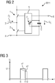
- FIG 2 shows the basic circuit diagram of one of the modules, based on the module M11 with the essential components.
- the other modules of the system are preferably constructed in the same way.
- the M11 module has two power connections 3 and 4, one of which is connection 3 at the node between switches 1 and 2.
- the second power connection 4 is at the other pole of the second switch 2.
- the contact of the switch 1 facing away from the power connection 3 is connected to the second power connection 4 via a capacitor C, which represents a voltage source of the module.
- the two switches 1 and 2 are controlled by a signal processing device 5. It has a communication connection 6 with which the local signal processing device 5, i.e. the signal processing device inside the module, with a control unit external to the module, which is integrated in FIG 2 is not shown, can come into communication.
- the signal processing device 5 preferably receives a control value from the external, central control unit, which is converted by the signal processing device 5 into specific control signals for the switches 1 and 2.
- the signal processing device 5 can be an FPGA or a microprocessor. If necessary, both are configured on site in order to control the module or the half-bridge in a suitable manner.
- the signal processing device 5 can optionally also be supplied with an auxiliary voltage via the communication connection 6, which the active components require for operation.
- the control value that the signal processing device 5 receives via the communication connection 6 from the control device external to the module is a voltage-time product value. This value therefore corresponds to a product of a voltage value and a time value.
- the voltage across the capacitor C which in the switched-on state also corresponds to the voltage across the power contacts 3 and 4, is measured by a voltmeter 7.
- This voltmeter 7 can be integrated into the signal processing device 5 or form a separate measuring device and be coupled to the signal processing device 5 for the transmission of the measured voltage value.
- the signal processing device 5 knows the current voltage value of the module M11, namely the voltage U C measured at the capacitor C. In addition, the signal processing device 5 has received a voltage-time product value for controlling the switches 1 and 2 from the external control unit via the communication connection 6. The signal processing device 5 now determines the switching times of switches 1 and 2 from both values. By dividing the product value by the measured voltage value, the signal processing device 5 receives a time value for the duration in which switch 1 should be closed and switch 2 open. If necessary, the time value is also determined in another way from the product value and the voltage value. Any parasitic effects can possibly be taken into account in this way. For example, the time value can also be determined using a special function or a simple assignment.
- the central control unit supplies a specific voltage-time product value as a control value, and a current voltage value U1 is measured.
- the voltage U1 would not change in the switch-on phase between times t0 and t1 corresponding to a voltage curve u1, and the switch-on time for switch 1 or the switch-off time for switch 2 in the simplest case would be the quotient between the product value and the voltage value correspond. In the present example, the time value would be t1.
- the voltage U C changes as a function of time. For example, the voltage curve u2 results after Switch-on time t0. The module voltage U C accordingly drops below the original value U1. However, since the module has received the product value U1 ⁇ (t1-t0) as a setpoint from the central control unit, the time of the pulse must be lengthened as its voltage drops.
- the signal processing device 5 now integrates the measured voltage u2 over the time t until the product value U1 ⁇ (t1-t0) is reached. In the present case, this is achieved at time t2. At this point in time t2, switch 1 is now opened and switch 2 is closed, so that module voltage U C drops to 0.
- the voltage-time area missing with a first pulse is only compensated for with the next pulse.
- the voltage value under voltage curve u2 is only integrated between times t0 and t1.
- the difference between the integral and the product U ⁇ (t1-t0), i.e. the integral under the voltage curve u1 is only taken into account with the next or another subsequent pulse, during which switch 1 is closed and switch 2 is open.
- the necessary voltage-time product values are transmitted to the module controller.
- the local module voltage measurement can be used, which enables a quick reaction to voltage changes. Such a rapid reaction to voltage changes is generally not possible if the measured voltage values first have to be transmitted from the modules to the central control unit.
- each module also has a local signal processing device, in particular a controller or FPGA, the PWM value to be delivered can now be used on each module on the basis of the currently available Module voltage (intermediate circuit voltage of the cell) and the target value, namely the voltage-time product value, can be calculated or determined.
- a local signal processing device in particular a controller or FPGA
- the measuring device and control logic of a module which are usually present anyway, can be used for the improved module control.
- the local decoupling of the control values to be determined e.g. PWM values
- the control values to be determined results in a better behavior of the overall system. It decouples the influences of fluctuating module voltages from the higher-level current and voltage regulators. This in turn enables a more dynamic adjustment of the required setpoints.
Landscapes
- Engineering & Computer Science (AREA)
- Power Engineering (AREA)
- Inverter Devices (AREA)
Priority Applications (3)
| Application Number | Priority Date | Filing Date | Title |
|---|---|---|---|
| PL16156307T PL3208930T3 (pl) | 2016-02-18 | 2016-02-18 | Modułowy przetwornik wielokomorowy z wewnątrzkomórkową kompensacją odchyleń napięciowych na kondensatorze ogniwa |
| EP16156307.7A EP3208930B1 (de) | 2016-02-18 | 2016-02-18 | Modularer mehrzellenumrichter mit zellinterner kompensation von spannungsschwankungen am zellkondensator |
| PCT/EP2016/078951 WO2017140393A1 (de) | 2016-02-18 | 2016-11-28 | Modularer mehrzellenumrichter mit zellinterner kompensation von spannungsschwankungen am zellkondensator |
Applications Claiming Priority (1)
| Application Number | Priority Date | Filing Date | Title |
|---|---|---|---|
| EP16156307.7A EP3208930B1 (de) | 2016-02-18 | 2016-02-18 | Modularer mehrzellenumrichter mit zellinterner kompensation von spannungsschwankungen am zellkondensator |
Publications (2)
| Publication Number | Publication Date |
|---|---|
| EP3208930A1 EP3208930A1 (de) | 2017-08-23 |
| EP3208930B1 true EP3208930B1 (de) | 2020-08-12 |
Family
ID=55442655
Family Applications (1)
| Application Number | Title | Priority Date | Filing Date |
|---|---|---|---|
| EP16156307.7A Active EP3208930B1 (de) | 2016-02-18 | 2016-02-18 | Modularer mehrzellenumrichter mit zellinterner kompensation von spannungsschwankungen am zellkondensator |
Country Status (3)
| Country | Link |
|---|---|
| EP (1) | EP3208930B1 (pl) |
| PL (1) | PL3208930T3 (pl) |
| WO (1) | WO2017140393A1 (pl) |
Family Cites Families (1)
| Publication number | Priority date | Publication date | Assignee | Title |
|---|---|---|---|---|
| JP5449893B2 (ja) * | 2009-07-21 | 2014-03-19 | 株式会社日立製作所 | 電力変換装置 |
-
2016
- 2016-02-18 PL PL16156307T patent/PL3208930T3/pl unknown
- 2016-02-18 EP EP16156307.7A patent/EP3208930B1/de active Active
- 2016-11-28 WO PCT/EP2016/078951 patent/WO2017140393A1/de not_active Ceased
Non-Patent Citations (1)
| Title |
|---|
| None * |
Also Published As
| Publication number | Publication date |
|---|---|
| WO2017140393A1 (de) | 2017-08-24 |
| EP3208930A1 (de) | 2017-08-23 |
| PL3208930T3 (pl) | 2021-01-25 |
Similar Documents
| Publication | Publication Date | Title |
|---|---|---|
| DE102020118242B3 (de) | Mehrebenen-Wechselrichter zur Erzeugung einer mehrstufigen Ausgangsspannung | |
| EP1927183B1 (de) | Verfahren zur steuerung eines mehrphasigen stromrichters mit verteilten energiespeichern | |
| EP3172821B1 (de) | Leistungselektronisches system zum betreiben einer last und verfahren zur synchronisation von leistungsmodulen | |
| EP3333005A1 (de) | Modulare leistungselektronik zum laden eines elektrisch betriebenen fahrzeugs | |
| EP2795783B1 (de) | System und verfahren zum ansteuern einer energiespeichereinrichtung | |
| WO1999041816A1 (de) | Vorrichtung und verfahren zum gesteuerten parallelbetrieb von gleichspannungswandlern | |
| DE102008032813A1 (de) | Netzanbindung von Solarzellen | |
| EP3198716B1 (de) | Verfahren zum erzeugen eines elektrischen wechselstroms | |
| EP2709257A2 (de) | Stromrichterschaltung und Verfahren zur Steuerung der Stromrichterschaltung | |
| EP2654190A2 (de) | Verfahren zum Betreiben einer elektrischen Schaltung | |
| EP2596980A2 (de) | Mehrpunkt-Stromrichter mit Bremschopper | |
| EP3151413A1 (de) | Steuervorrichtung und steuerverfahren für grosse stromrichter | |
| EP2807738B1 (de) | Multizellenkonverter | |
| EP3220527A1 (de) | Modularer mehrstufenumrichter | |
| EP3449554B1 (de) | Wechselrichter und verfahren zum erzeugen eines wechselstroms | |
| DE102015222280A1 (de) | Modularer Mehrstufenumrichter und Verfahren zum Betreiben eines modularen Mehrstufenumrichters | |
| DE19650994C1 (de) | Verfahren zur Pulsweitenmodulation einer Sollspannung für 3-Level-Vierquadrantensteller mit Berücksichtigung der Mindestschaltzeiten der Leistungshalbleiterschalter | |
| EP3208930A1 (de) | Modularer mehrzellenumrichter mit zellinterner kompensation von spannungsschwankungen am zellkondensator | |
| EP3363091B1 (de) | Vorrichtung und verfahren zum steuern eines lastflusses in einem wechselspannungsnetz | |
| DE102013109714A1 (de) | Verfahren zum Betreiben einer elektrischen Schaltung sowie elektrische Schaltung | |
| WO2014095233A2 (de) | Batterie mit mindestens einem batteriestrang sowie verfahren zur regelung einer batteriespannung | |
| EP3218980B1 (de) | Verfahren zum steuern eines lastflusses in einem gleichspannungsnetz | |
| WO2013186006A2 (de) | Multizellenkonverter | |
| WO2013064318A2 (de) | Spannungswandler mit einer ersten parallelschaltung | |
| EP3331118B1 (de) | Anlage zum übertragen elektrischer leistung |
Legal Events
| Date | Code | Title | Description |
|---|---|---|---|
| PUAI | Public reference made under article 153(3) epc to a published international application that has entered the european phase |
Free format text: ORIGINAL CODE: 0009012 |
|
| STAA | Information on the status of an ep patent application or granted ep patent |
Free format text: STATUS: THE APPLICATION HAS BEEN PUBLISHED |
|
| AK | Designated contracting states |
Kind code of ref document: A1 Designated state(s): AL AT BE BG CH CY CZ DE DK EE ES FI FR GB GR HR HU IE IS IT LI LT LU LV MC MK MT NL NO PL PT RO RS SE SI SK SM TR |
|
| AX | Request for extension of the european patent |
Extension state: BA ME |
|
| RAP1 | Party data changed (applicant data changed or rights of an application transferred) |
Owner name: SIEMENS AKTIENGESELLSCHAFT |
|
| STAA | Information on the status of an ep patent application or granted ep patent |
Free format text: STATUS: REQUEST FOR EXAMINATION WAS MADE |
|
| 17P | Request for examination filed |
Effective date: 20180222 |
|
| RBV | Designated contracting states (corrected) |
Designated state(s): AL AT BE BG CH CY CZ DE DK EE ES FI FR GB GR HR HU IE IS IT LI LT LU LV MC MK MT NL NO PL PT RO RS SE SI SK SM TR |
|
| GRAP | Despatch of communication of intention to grant a patent |
Free format text: ORIGINAL CODE: EPIDOSNIGR1 |
|
| STAA | Information on the status of an ep patent application or granted ep patent |
Free format text: STATUS: GRANT OF PATENT IS INTENDED |
|
| INTG | Intention to grant announced |
Effective date: 20200409 |
|
| GRAS | Grant fee paid |
Free format text: ORIGINAL CODE: EPIDOSNIGR3 |
|
| GRAA | (expected) grant |
Free format text: ORIGINAL CODE: 0009210 |
|
| STAA | Information on the status of an ep patent application or granted ep patent |
Free format text: STATUS: THE PATENT HAS BEEN GRANTED |
|
| AK | Designated contracting states |
Kind code of ref document: B1 Designated state(s): AL AT BE BG CH CY CZ DE DK EE ES FI FR GB GR HR HU IE IS IT LI LT LU LV MC MK MT NL NO PL PT RO RS SE SI SK SM TR |
|
| REG | Reference to a national code |
Ref country code: CH Ref legal event code: EP |
|
| REG | Reference to a national code |
Ref country code: IE Ref legal event code: FG4D Free format text: LANGUAGE OF EP DOCUMENT: GERMAN |
|
| REG | Reference to a national code |
Ref country code: DE Ref legal event code: R096 Ref document number: 502016010792 Country of ref document: DE |
|
| REG | Reference to a national code |
Ref country code: AT Ref legal event code: REF Ref document number: 1302541 Country of ref document: AT Kind code of ref document: T Effective date: 20200915 |
|
| REG | Reference to a national code |
Ref country code: CH Ref legal event code: NV Representative=s name: SIEMENS SCHWEIZ AG, CH |
|
| REG | Reference to a national code |
Ref country code: SE Ref legal event code: TRGR |
|
| REG | Reference to a national code |
Ref country code: DE Ref legal event code: R081 Ref document number: 502016010792 Country of ref document: DE Owner name: SIEMENS ENERGY GLOBAL GMBH & CO. KG, DE Free format text: FORMER OWNER: SIEMENS AKTIENGESELLSCHAFT, 80333 MUENCHEN, DE |
|
| REG | Reference to a national code |
Ref country code: LT Ref legal event code: MG4D |
|
| REG | Reference to a national code |
Ref country code: NL Ref legal event code: MP Effective date: 20200812 |
|
| RAP2 | Party data changed (patent owner data changed or rights of a patent transferred) |
Owner name: SIEMENS ENERGY GLOBAL GMBH & CO. KG |
|
| PG25 | Lapsed in a contracting state [announced via postgrant information from national office to epo] |
Ref country code: BG Free format text: LAPSE BECAUSE OF FAILURE TO SUBMIT A TRANSLATION OF THE DESCRIPTION OR TO PAY THE FEE WITHIN THE PRESCRIBED TIME-LIMIT Effective date: 20201112 Ref country code: GR Free format text: LAPSE BECAUSE OF FAILURE TO SUBMIT A TRANSLATION OF THE DESCRIPTION OR TO PAY THE FEE WITHIN THE PRESCRIBED TIME-LIMIT Effective date: 20201113 Ref country code: NO Free format text: LAPSE BECAUSE OF FAILURE TO SUBMIT A TRANSLATION OF THE DESCRIPTION OR TO PAY THE FEE WITHIN THE PRESCRIBED TIME-LIMIT Effective date: 20201112 Ref country code: FI Free format text: LAPSE BECAUSE OF FAILURE TO SUBMIT A TRANSLATION OF THE DESCRIPTION OR TO PAY THE FEE WITHIN THE PRESCRIBED TIME-LIMIT Effective date: 20200812 Ref country code: HR Free format text: LAPSE BECAUSE OF FAILURE TO SUBMIT A TRANSLATION OF THE DESCRIPTION OR TO PAY THE FEE WITHIN THE PRESCRIBED TIME-LIMIT Effective date: 20200812 Ref country code: LT Free format text: LAPSE BECAUSE OF FAILURE TO SUBMIT A TRANSLATION OF THE DESCRIPTION OR TO PAY THE FEE WITHIN THE PRESCRIBED TIME-LIMIT Effective date: 20200812 |
|
| PG25 | Lapsed in a contracting state [announced via postgrant information from national office to epo] |
Ref country code: IS Free format text: LAPSE BECAUSE OF FAILURE TO SUBMIT A TRANSLATION OF THE DESCRIPTION OR TO PAY THE FEE WITHIN THE PRESCRIBED TIME-LIMIT Effective date: 20201212 Ref country code: LV Free format text: LAPSE BECAUSE OF FAILURE TO SUBMIT A TRANSLATION OF THE DESCRIPTION OR TO PAY THE FEE WITHIN THE PRESCRIBED TIME-LIMIT Effective date: 20200812 Ref country code: RS Free format text: LAPSE BECAUSE OF FAILURE TO SUBMIT A TRANSLATION OF THE DESCRIPTION OR TO PAY THE FEE WITHIN THE PRESCRIBED TIME-LIMIT Effective date: 20200812 Ref country code: NL Free format text: LAPSE BECAUSE OF FAILURE TO SUBMIT A TRANSLATION OF THE DESCRIPTION OR TO PAY THE FEE WITHIN THE PRESCRIBED TIME-LIMIT Effective date: 20200812 |
|
| PG25 | Lapsed in a contracting state [announced via postgrant information from national office to epo] |
Ref country code: EE Free format text: LAPSE BECAUSE OF FAILURE TO SUBMIT A TRANSLATION OF THE DESCRIPTION OR TO PAY THE FEE WITHIN THE PRESCRIBED TIME-LIMIT Effective date: 20200812 Ref country code: RO Free format text: LAPSE BECAUSE OF FAILURE TO SUBMIT A TRANSLATION OF THE DESCRIPTION OR TO PAY THE FEE WITHIN THE PRESCRIBED TIME-LIMIT Effective date: 20200812 Ref country code: SM Free format text: LAPSE BECAUSE OF FAILURE TO SUBMIT A TRANSLATION OF THE DESCRIPTION OR TO PAY THE FEE WITHIN THE PRESCRIBED TIME-LIMIT Effective date: 20200812 Ref country code: CZ Free format text: LAPSE BECAUSE OF FAILURE TO SUBMIT A TRANSLATION OF THE DESCRIPTION OR TO PAY THE FEE WITHIN THE PRESCRIBED TIME-LIMIT Effective date: 20200812 Ref country code: DK Free format text: LAPSE BECAUSE OF FAILURE TO SUBMIT A TRANSLATION OF THE DESCRIPTION OR TO PAY THE FEE WITHIN THE PRESCRIBED TIME-LIMIT Effective date: 20200812 |
|
| REG | Reference to a national code |
Ref country code: DE Ref legal event code: R097 Ref document number: 502016010792 Country of ref document: DE |
|
| PG25 | Lapsed in a contracting state [announced via postgrant information from national office to epo] |
Ref country code: AL Free format text: LAPSE BECAUSE OF FAILURE TO SUBMIT A TRANSLATION OF THE DESCRIPTION OR TO PAY THE FEE WITHIN THE PRESCRIBED TIME-LIMIT Effective date: 20200812 Ref country code: ES Free format text: LAPSE BECAUSE OF FAILURE TO SUBMIT A TRANSLATION OF THE DESCRIPTION OR TO PAY THE FEE WITHIN THE PRESCRIBED TIME-LIMIT Effective date: 20200812 |
|
| PLBE | No opposition filed within time limit |
Free format text: ORIGINAL CODE: 0009261 |
|
| STAA | Information on the status of an ep patent application or granted ep patent |
Free format text: STATUS: NO OPPOSITION FILED WITHIN TIME LIMIT |
|
| PG25 | Lapsed in a contracting state [announced via postgrant information from national office to epo] |
Ref country code: SK Free format text: LAPSE BECAUSE OF FAILURE TO SUBMIT A TRANSLATION OF THE DESCRIPTION OR TO PAY THE FEE WITHIN THE PRESCRIBED TIME-LIMIT Effective date: 20200812 |
|
| 26N | No opposition filed |
Effective date: 20210514 |
|
| PG25 | Lapsed in a contracting state [announced via postgrant information from national office to epo] |
Ref country code: SI Free format text: LAPSE BECAUSE OF FAILURE TO SUBMIT A TRANSLATION OF THE DESCRIPTION OR TO PAY THE FEE WITHIN THE PRESCRIBED TIME-LIMIT Effective date: 20200812 |
|
| PG25 | Lapsed in a contracting state [announced via postgrant information from national office to epo] |
Ref country code: MC Free format text: LAPSE BECAUSE OF FAILURE TO SUBMIT A TRANSLATION OF THE DESCRIPTION OR TO PAY THE FEE WITHIN THE PRESCRIBED TIME-LIMIT Effective date: 20200812 |
|
| REG | Reference to a national code |
Ref country code: BE Ref legal event code: MM Effective date: 20210228 |
|
| PG25 | Lapsed in a contracting state [announced via postgrant information from national office to epo] |
Ref country code: LU Free format text: LAPSE BECAUSE OF NON-PAYMENT OF DUE FEES Effective date: 20210218 |
|
| REG | Reference to a national code |
Ref country code: GB Ref legal event code: 732E Free format text: REGISTERED BETWEEN 20211202 AND 20211209 |
|
| PG25 | Lapsed in a contracting state [announced via postgrant information from national office to epo] |
Ref country code: IE Free format text: LAPSE BECAUSE OF NON-PAYMENT OF DUE FEES Effective date: 20210218 |
|
| REG | Reference to a national code |
Ref country code: AT Ref legal event code: MM01 Ref document number: 1302541 Country of ref document: AT Kind code of ref document: T Effective date: 20210218 |
|
| PG25 | Lapsed in a contracting state [announced via postgrant information from national office to epo] |
Ref country code: AT Free format text: LAPSE BECAUSE OF NON-PAYMENT OF DUE FEES Effective date: 20210218 |
|
| PG25 | Lapsed in a contracting state [announced via postgrant information from national office to epo] |
Ref country code: BE Free format text: LAPSE BECAUSE OF NON-PAYMENT OF DUE FEES Effective date: 20210228 |
|
| PG25 | Lapsed in a contracting state [announced via postgrant information from national office to epo] |
Ref country code: PT Free format text: LAPSE BECAUSE OF FAILURE TO SUBMIT A TRANSLATION OF THE DESCRIPTION OR TO PAY THE FEE WITHIN THE PRESCRIBED TIME-LIMIT Effective date: 20201214 |
|
| PG25 | Lapsed in a contracting state [announced via postgrant information from national office to epo] |
Ref country code: HU Free format text: LAPSE BECAUSE OF FAILURE TO SUBMIT A TRANSLATION OF THE DESCRIPTION OR TO PAY THE FEE WITHIN THE PRESCRIBED TIME-LIMIT; INVALID AB INITIO Effective date: 20160218 |
|
| PG25 | Lapsed in a contracting state [announced via postgrant information from national office to epo] |
Ref country code: CY Free format text: LAPSE BECAUSE OF FAILURE TO SUBMIT A TRANSLATION OF THE DESCRIPTION OR TO PAY THE FEE WITHIN THE PRESCRIBED TIME-LIMIT Effective date: 20200812 |
|
| P01 | Opt-out of the competence of the unified patent court (upc) registered |
Effective date: 20231222 |
|
| PG25 | Lapsed in a contracting state [announced via postgrant information from national office to epo] |
Ref country code: MK Free format text: LAPSE BECAUSE OF FAILURE TO SUBMIT A TRANSLATION OF THE DESCRIPTION OR TO PAY THE FEE WITHIN THE PRESCRIBED TIME-LIMIT Effective date: 20200812 |
|
| PG25 | Lapsed in a contracting state [announced via postgrant information from national office to epo] |
Ref country code: MT Free format text: LAPSE BECAUSE OF FAILURE TO SUBMIT A TRANSLATION OF THE DESCRIPTION OR TO PAY THE FEE WITHIN THE PRESCRIBED TIME-LIMIT Effective date: 20200812 |
|
| PG25 | Lapsed in a contracting state [announced via postgrant information from national office to epo] |
Ref country code: TR Free format text: LAPSE BECAUSE OF FAILURE TO SUBMIT A TRANSLATION OF THE DESCRIPTION OR TO PAY THE FEE WITHIN THE PRESCRIBED TIME-LIMIT Effective date: 20200812 |
|
| REG | Reference to a national code |
Ref country code: CH Ref legal event code: U11 Free format text: ST27 STATUS EVENT CODE: U-0-0-U10-U11 (AS PROVIDED BY THE NATIONAL OFFICE) Effective date: 20260301 |
|
| PGFP | Annual fee paid to national office [announced via postgrant information from national office to epo] |
Ref country code: SE Payment date: 20260223 Year of fee payment: 11 |
|
| PGFP | Annual fee paid to national office [announced via postgrant information from national office to epo] |
Ref country code: GB Payment date: 20260223 Year of fee payment: 11 |
|
| PGFP | Annual fee paid to national office [announced via postgrant information from national office to epo] |
Ref country code: DE Payment date: 20260220 Year of fee payment: 11 |
|
| PGFP | Annual fee paid to national office [announced via postgrant information from national office to epo] |
Ref country code: IT Payment date: 20260220 Year of fee payment: 11 |
|
| PGFP | Annual fee paid to national office [announced via postgrant information from national office to epo] |
Ref country code: FR Payment date: 20260224 Year of fee payment: 11 |
|
| PGFP | Annual fee paid to national office [announced via postgrant information from national office to epo] |
Ref country code: CH Payment date: 20260301 Year of fee payment: 11 |
|
| PGFP | Annual fee paid to national office [announced via postgrant information from national office to epo] |
Ref country code: PL Payment date: 20260126 Year of fee payment: 11 |