EP3208610A1 - Sensor arrangement and method for generating measurement signals - Google Patents
Sensor arrangement and method for generating measurement signals Download PDFInfo
- Publication number
- EP3208610A1 EP3208610A1 EP16156345.7A EP16156345A EP3208610A1 EP 3208610 A1 EP3208610 A1 EP 3208610A1 EP 16156345 A EP16156345 A EP 16156345A EP 3208610 A1 EP3208610 A1 EP 3208610A1
- Authority
- EP
- European Patent Office
- Prior art keywords
- electrode line
- electrode
- sensor arrangement
- sensitive layer
- electrode lines
- Prior art date
- Legal status (The legal status is an assumption and is not a legal conclusion. Google has not performed a legal analysis and makes no representation as to the accuracy of the status listed.)
- Granted
Links
- 238000005259 measurement Methods 0.000 title claims abstract description 98
- 238000000034 method Methods 0.000 title claims description 13
- 230000008961 swelling Effects 0.000 claims description 23
- 230000006870 function Effects 0.000 claims description 14
- 229920001721 polyimide Polymers 0.000 claims description 8
- 239000004642 Polyimide Substances 0.000 claims description 7
- XLYOFNOQVPJJNP-UHFFFAOYSA-N water Substances O XLYOFNOQVPJJNP-UHFFFAOYSA-N 0.000 claims description 7
- 238000012937 correction Methods 0.000 claims description 5
- 230000008929 regeneration Effects 0.000 claims description 4
- 238000011069 regeneration method Methods 0.000 claims description 4
- 239000007789 gas Substances 0.000 description 53
- 238000001465 metallisation Methods 0.000 description 33
- 229920000642 polymer Polymers 0.000 description 32
- 239000004065 semiconductor Substances 0.000 description 30
- 239000000758 substrate Substances 0.000 description 26
- 230000005684 electric field Effects 0.000 description 19
- 239000000463 material Substances 0.000 description 16
- 239000003990 capacitor Substances 0.000 description 12
- 230000035945 sensitivity Effects 0.000 description 12
- 230000008859 change Effects 0.000 description 9
- 229910052751 metal Inorganic materials 0.000 description 8
- 239000002184 metal Substances 0.000 description 8
- 239000003570 air Substances 0.000 description 7
- 230000008569 process Effects 0.000 description 7
- 238000004088 simulation Methods 0.000 description 7
- 230000002441 reversible effect Effects 0.000 description 6
- 238000000151 deposition Methods 0.000 description 5
- 230000008021 deposition Effects 0.000 description 5
- 238000011161 development Methods 0.000 description 5
- 230000018109 developmental process Effects 0.000 description 5
- VYPSYNLAJGMNEJ-UHFFFAOYSA-N Silicium dioxide Chemical compound O=[Si]=O VYPSYNLAJGMNEJ-UHFFFAOYSA-N 0.000 description 4
- 230000000694 effects Effects 0.000 description 4
- 238000011084 recovery Methods 0.000 description 4
- 239000012080 ambient air Substances 0.000 description 3
- 238000004364 calculation method Methods 0.000 description 3
- 230000007423 decrease Effects 0.000 description 3
- 238000001514 detection method Methods 0.000 description 3
- 238000005530 etching Methods 0.000 description 3
- 238000012545 processing Methods 0.000 description 3
- 239000000126 substance Substances 0.000 description 3
- 229910052581 Si3N4 Inorganic materials 0.000 description 2
- 230000001419 dependent effect Effects 0.000 description 2
- 239000012621 metal-organic framework Substances 0.000 description 2
- 238000000059 patterning Methods 0.000 description 2
- 230000035515 penetration Effects 0.000 description 2
- BASFCYQUMIYNBI-UHFFFAOYSA-N platinum Chemical compound [Pt] BASFCYQUMIYNBI-UHFFFAOYSA-N 0.000 description 2
- 239000000523 sample Substances 0.000 description 2
- 235000012239 silicon dioxide Nutrition 0.000 description 2
- 239000000377 silicon dioxide Substances 0.000 description 2
- HQVNEWCFYHHQES-UHFFFAOYSA-N silicon nitride Chemical compound N12[Si]34N5[Si]62N3[Si]51N64 HQVNEWCFYHHQES-UHFFFAOYSA-N 0.000 description 2
- RYGMFSIKBFXOCR-UHFFFAOYSA-N Copper Chemical compound [Cu] RYGMFSIKBFXOCR-UHFFFAOYSA-N 0.000 description 1
- 229910052782 aluminium Inorganic materials 0.000 description 1
- XAGFODPZIPBFFR-UHFFFAOYSA-N aluminium Chemical compound [Al] XAGFODPZIPBFFR-UHFFFAOYSA-N 0.000 description 1
- 230000006399 behavior Effects 0.000 description 1
- 239000013590 bulk material Substances 0.000 description 1
- 230000000295 complement effect Effects 0.000 description 1
- 229910052802 copper Inorganic materials 0.000 description 1
- 239000010949 copper Substances 0.000 description 1
- 230000008878 coupling Effects 0.000 description 1
- 238000010168 coupling process Methods 0.000 description 1
- 238000005859 coupling reaction Methods 0.000 description 1
- 230000003247 decreasing effect Effects 0.000 description 1
- 238000009792 diffusion process Methods 0.000 description 1
- 230000005669 field effect Effects 0.000 description 1
- 239000011521 glass Substances 0.000 description 1
- 229930195733 hydrocarbon Natural products 0.000 description 1
- 150000002430 hydrocarbons Chemical class 0.000 description 1
- 230000000977 initiatory effect Effects 0.000 description 1
- 230000010354 integration Effects 0.000 description 1
- 239000002608 ionic liquid Substances 0.000 description 1
- 230000002427 irreversible effect Effects 0.000 description 1
- 239000007788 liquid Substances 0.000 description 1
- 238000004519 manufacturing process Methods 0.000 description 1
- 229910044991 metal oxide Inorganic materials 0.000 description 1
- 150000004706 metal oxides Chemical class 0.000 description 1
- 230000003278 mimic effect Effects 0.000 description 1
- 238000012986 modification Methods 0.000 description 1
- 230000004048 modification Effects 0.000 description 1
- 238000002161 passivation Methods 0.000 description 1
- 229910052697 platinum Inorganic materials 0.000 description 1
- 230000010287 polarization Effects 0.000 description 1
- 229910021420 polycrystalline silicon Inorganic materials 0.000 description 1
- 239000002861 polymer material Substances 0.000 description 1
- 229920005591 polysilicon Polymers 0.000 description 1
- 230000000630 rising effect Effects 0.000 description 1
- 229910021332 silicide Inorganic materials 0.000 description 1
- FVBUAEGBCNSCDD-UHFFFAOYSA-N silicide(4-) Chemical compound [Si-4] FVBUAEGBCNSCDD-UHFFFAOYSA-N 0.000 description 1
- 230000007704 transition Effects 0.000 description 1
- WFKWXMTUELFFGS-UHFFFAOYSA-N tungsten Chemical compound [W] WFKWXMTUELFFGS-UHFFFAOYSA-N 0.000 description 1
- 229910052721 tungsten Inorganic materials 0.000 description 1
- 239000010937 tungsten Substances 0.000 description 1
Images


Classifications
-
- G—PHYSICS
- G01—MEASURING; TESTING
- G01N—INVESTIGATING OR ANALYSING MATERIALS BY DETERMINING THEIR CHEMICAL OR PHYSICAL PROPERTIES
- G01N27/00—Investigating or analysing materials by the use of electric, electrochemical, or magnetic means
- G01N27/02—Investigating or analysing materials by the use of electric, electrochemical, or magnetic means by investigating impedance
- G01N27/22—Investigating or analysing materials by the use of electric, electrochemical, or magnetic means by investigating impedance by investigating capacitance
- G01N27/226—Construction of measuring vessels; Electrodes therefor
-
- G—PHYSICS
- G01—MEASURING; TESTING
- G01N—INVESTIGATING OR ANALYSING MATERIALS BY DETERMINING THEIR CHEMICAL OR PHYSICAL PROPERTIES
- G01N27/00—Investigating or analysing materials by the use of electric, electrochemical, or magnetic means
- G01N27/02—Investigating or analysing materials by the use of electric, electrochemical, or magnetic means by investigating impedance
- G01N27/22—Investigating or analysing materials by the use of electric, electrochemical, or magnetic means by investigating impedance by investigating capacitance
- G01N27/221—Investigating or analysing materials by the use of electric, electrochemical, or magnetic means by investigating impedance by investigating capacitance by investigating the dielectric properties
-
- G—PHYSICS
- G01—MEASURING; TESTING
- G01N—INVESTIGATING OR ANALYSING MATERIALS BY DETERMINING THEIR CHEMICAL OR PHYSICAL PROPERTIES
- G01N27/00—Investigating or analysing materials by the use of electric, electrochemical, or magnetic means
- G01N27/02—Investigating or analysing materials by the use of electric, electrochemical, or magnetic means by investigating impedance
- G01N27/22—Investigating or analysing materials by the use of electric, electrochemical, or magnetic means by investigating impedance by investigating capacitance
- G01N27/223—Investigating or analysing materials by the use of electric, electrochemical, or magnetic means by investigating impedance by investigating capacitance for determining moisture content, e.g. humidity
-
- G—PHYSICS
- G01—MEASURING; TESTING
- G01R—MEASURING ELECTRIC VARIABLES; MEASURING MAGNETIC VARIABLES
- G01R27/00—Arrangements for measuring resistance, reactance, impedance, or electric characteristics derived therefrom
- G01R27/02—Measuring real or complex resistance, reactance, impedance, or other two-pole characteristics derived therefrom, e.g. time constant
- G01R27/26—Measuring inductance or capacitance; Measuring quality factor, e.g. by using the resonance method; Measuring loss factor; Measuring dielectric constants ; Measuring impedance or related variables
- G01R27/2605—Measuring capacitance
-
- G—PHYSICS
- G01—MEASURING; TESTING
- G01N—INVESTIGATING OR ANALYSING MATERIALS BY DETERMINING THEIR CHEMICAL OR PHYSICAL PROPERTIES
- G01N27/00—Investigating or analysing materials by the use of electric, electrochemical, or magnetic means
- G01N27/02—Investigating or analysing materials by the use of electric, electrochemical, or magnetic means by investigating impedance
- G01N27/22—Investigating or analysing materials by the use of electric, electrochemical, or magnetic means by investigating impedance by investigating capacitance
- G01N27/221—Investigating or analysing materials by the use of electric, electrochemical, or magnetic means by investigating impedance by investigating capacitance by investigating the dielectric properties
- G01N2027/222—Investigating or analysing materials by the use of electric, electrochemical, or magnetic means by investigating impedance by investigating capacitance by investigating the dielectric properties for analysing gases
Definitions
- the present invention is related to a sensor arrangement and a method for generating measurement signals.
- the sensor arrangement is configured as a chemical sensor arrangement.
- the sensor arrangement is designed for the measurement of a parameter in a gas or a liquid.
- the sensor arrangement may be realized for the detection of humidity, i.e. for the detection of water molecules in air.
- a capacitive sensor with a sensitive layer is often used for humidity detection.
- the humidity may change several parameters of the sensitive layer. However, only one parameter of the sensitive layer is commonly measured.
- a sensor arrangement comprises a capacitive sensor and a readout circuit.
- the capacitive sensor comprises a first electrode line, a second electrode line, a third electrode line and a sensitive layer.
- the sensitive layer is arranged at the first, the second and the third electrode lines.
- the readout circuit comprises a capacitance-to-digital converter, abbreviated converter.
- the readout circuit is coupled to the first, the second and the third electrode lines.
- the readout circuit is configured to generate a first measurement signal using the first and the second electrode lines and to generate a second measurement signal using at least the third electrode line.
- the first, second and third electrode lines are arranged at the sensitive layer, more than one measurement signal can be generated and, thus, more than one parameter of the sensitive layer can be measured.
- the sensor arrangement allows more information to be gained out of the sensitive layer.
- the sensitive layer is in contact with the first, the second and the third electrode lines.
- the converter is coupled on its input side to the first, the second and the third electrode lines.
- the converter generates the first measurement signals and the second measurement signal.
- the converter is coupled on its input side to the first and the second electrode lines.
- the converter generates the first measurement signal.
- the readout circuit comprises a further capacitance-to-digital converter - abbreviated further converter - that is coupled at least to the third electrode line.
- the further converter generates the second measurement signal.
- the sensor arrangement is realized as a chemical sensor arrangement.
- the chemical sensor arrangement may be implemented as a gas sensor arrangement.
- the gas sensor arrangement may be configured as a humidity sensor arrangement. Since water molecules are an example for a gas, a humidity sensor arrangement is an embodiment of a gas sensor arrangement.
- the sensitive layer is designed to absorb a gas to be detected, such as CO 2 or SO 2 .
- the sensitive layer may change its permittivity depending on the absorbed gas.
- the sensitive layer may change its capacitance and/or its resistance depending on the absorbed gas.
- the gas absorbed by sensitive layer are water molecules, H 2 0.
- a humidity sensor often has a different behavior than a gas sensor for other gases, since water molecules are not burnable such as CO or hydrocarbons, have a high concentration and have an upper limit in air.
- the sensitive layer may be a polymer.
- the sensitive layer may be made of a polyimide.
- the first, the second and the third electrode lines are configured such that the first measurement signal depends more on a swelling of the sensitive layer than the second measurement signal.
- the swelling of the sensitive layer may occur, when the sensitive layer absorbs the gas to be detected, for example the water molecules.
- the first measurement signal depends more on the changing thickness of the sensitive layer than the second measurement signal.
- the sensitive layer increases its thickness by the swelling.
- the swelling may be a reversible swelling, a permanent swelling or a swelling that is partially reversible and partially permanent.
- a reversible swelling the thickness of the sensitive layer increases with rising concentration of the gas to be detected, e.g. humidity, and decreases with decreasing concentration of the gas to be detected, e.g. humidity.
- a permanent swelling the thickness of the sensitive layer does not decrease, when the concentration of the gas to be detected, e.g. humidity, decreases.
- the first, the second and the third electrode lines are configured such that the second measurement signal depends more on the bulk properties of the sensitive layer than the first measurement signal.
- the readout circuit provides a gas signal as a function of the first measurement signal and the second measurement signal.
- the gas signal may be a humidity signal.
- the readout circuit may have a digital processor coupled to the converter.
- the digital processor of the readout circuit is coupled to the converter and the further converter.
- the digital processor may be implemented as a microcontroller, a microprocessor or a state machine.
- the readout circuit may comprises a memory coupled to the digital processor.
- the digital processor may calculate the gas signal.
- the digital processor calculates the gas signal using an equation and/or a look-up table with the first and the second measurement signals as inputs.
- the digital processor calculates a first gas signal using a first equation and/or a first look-up table with the first measurement signal as an input. Moreover, the digital processor calculates a second gas signal using a second equation and/or a second look-up table and using the second measurement signal as an input. The gas signal may be calculated by the digital processor as an average value of the first and the second gas signal.
- the readout circuit provides a drift signal as a function of the first and the second measurement signal.
- the digital processor may perform the calculation of the drift signal.
- the digital processor may provide the drift signal as a function of the first and the second measurement signal and data stored in the memory.
- the digital processor may calculate the drift signal using the first and the second gas signals as inputs.
- the drift signal has a value indicating a drift, when the first gas signal is different from the second gas signal.
- the value of the drift signal may be a function of the difference between the first and the second gas signal, e.g. may be proportional to said difference.
- the readout circuit compares the first and the second measurement signal with correlation data stored in the memory.
- the readout circuit calculates the drift signal depending on the result of the comparison. If the first and the second measurement signal correlate to each other, the readout circuit may calculate a value of the drift signal indicating an absence of a drift. In case the first and the second measurement signal have only a small or none correlation, the readout circuit calculates the drift signal with a value indicating a drift.
- the sensor arrangement performs an offset correction, generates a warning signal and/or starts a regeneration cycle depending on the value of the drift signal.
- the readout circuit may be configured to compare the value of the drift signal with a threshold value and to generate the warning signal, to start the regeneration cycle and/or to perform the offset correction in case the drift signal is higher than the threshold value.
- the readout circuit may perform an offset correction for each value of the drift signal that indicates a drift.
- the capacitive sensor comprises a fourth electrode line.
- the sensitive layer is arranged at the fourth electrode line.
- the fourth electrode line is coupled to the readout circuit.
- the readout circuit is configured to generate the second measurement signal using the third and the fourth electrode lines.
- the converter may be coupled on its input side to the third and the fourth electrode lines.
- the readout circuit comprises the converter and the further converter
- the further converter is coupled on its input side to the third and fourth electrode lines.
- the converter is coupled on its input side to the first and second electrode lines.
- a distance of the first and second electrode lines to an interface between the sensitive layer and an ambient gas is less than a distance of the third and fourth electrode lines to said interface.
- the first to the fourth electrode lines may be arranged in different planes.
- a change of a parameter at the interface can be detected by the first and second electrode lines and changes the first measurement signal to a higher extent than the second measurement signal.
- a change in the bulk of the sensitive layer can be more easily detected by the third and fourth electrode lines and, thus, changes the second measurement signal to a higher extent than the first measurement signal.
- the capacitive sensor comprises a semiconductor substrate and at least a dielectric layer on top of the semiconductor substrate.
- a distance of the first and second electrode lines to the semiconductor substrate is larger than a distance of the third and fourth electrode lines to the semiconductor substrate.
- the third and the fourth electrode lines may be covered by the sensitive layer.
- the third and fourth electrode lines may each have a top surface that is covered by the sensitive layer.
- the third and fourth electrode lines may have side surface that are covered by the sensitive layer.
- the first and the second electrode lines are covered by the sensitive layer.
- the first and the second electrode lines are only partially covered by the sensitive layer.
- the top surface of the first and the second electrode line may be free from the sensitive layer.
- only a part of the side surfaces of the first and second electrode line may be in contact with the sensitive layer.
- an interface of the sensitive layer and the ambient air is below the top surface and above a bottom surface of the first and second electrode lines.
- said interface may be in the midst of the top surface and the bottom surface.
- said interface may be in the midst of the side surfaces of the first and second electrode lines.
- the sensitive layer may not be perfectly flat.
- a thickness of the sensitive layer may be higher adjacent to the first and second electrode lines than in an area between the first and the second electrode lines.
- an average thickness of the sensitive layer and an average interface of the sensitive layer to the ambient air can be defined.
- an average interface of the sensitive layer to the ambient air is below the top surface and above the bottom surface of the first and second electrode lines.
- the first, the second and the third electrode lines are arranged in a plane. A distance of the first, the second and the third electrode lines to a semiconductor substrate of the capacitive sensor is approximately identical.
- a distance of the first electrode line to the second electrode line is larger than a distance of the first electrode line to the third electrode line.
- the readout circuit generates the first measurement signal by a capacitance measurement between the first and the second electrode line. Moreover, the readout circuit generates the second measurement signal by a capacitance measurement between the first and the third electrode line.
- the first and the second electrode lines are coupled to the converter in a first phase and the first and the third electrode line are coupled to the converter in a second phase. Due to the small distance of the first electrode line to the third electrode line, the second measurement signal depends more on the bulk parameter of the sensitive layer than the first measurement signal. Due to the larger distance of the first electrode line to the second electrode line, the first measurement signal depends more on parameters at the surface of the sensitive layer than the second measurement signal.
- the capacitive sensor comprises a transducer layout configured to track permanent material changes, such as permanent changes of the sensitive layer.
- the sensor arrangement may perform active cancellation of sensor drift.
- the sensor arrangement may track differences in capacitive readout due to material changes (i.e. swelling) and bulk dielectric constant changes, thus detecting and decoupling drift (or permanent capacitive change) from regular dielectric changes.
- the sensor arrangement is able to counteract a drift in the sensitive layer.
- Sensor drift can often be attributed to bulk effects of the sensitive layer that is also called material or gas sensitive layer.
- the sensor arrangement may use at least two material properties to determine the gas concentration or the relative humidity. As a result, the accuracy of the sensor read-out increases.
- the sensor arrangement may able to identify when a recovery treatment is required. Such a recovery treatment may return the material, e.g. the sensitive layer, to its original state.
- the sensor arrangement may include tracking whether permanent changes in the relative humidity sensitive bulk material occur.
- the sensor arrangement may include to identify drift to initiate countermeasures to these effects.
- the sensor arrangement simultaneously monitors multiple types of drift (permanent swelling and dielectric constant drift) in the gas sensitive material and determines the conditions for initiating countermeasures.
- the sensor arrangement identifies drift and triggers a warning or on-chip countermeasures.
- the sensor arrangement may be designed to track two different material properties by two capacitive measurements. This is realized by adjusting the transducer layout (including different electrode sets) or/and by applying different electrode polarization on the same electrode set.
- the sensor arrangement may be designed to identify drift.
- the two capacitive measurements are compared continuously.
- a correlation plot or correlation data between relative humidity - (reversible) swelling - (reversible) dielectric constant exists. If irreversible swelling occurs, the dimensional material changes will not correspond any more with dielectric constant changes according to the pre-drift correlation.
- the double capacitive measurement of the sensor arrangement identifies the deviation from this correlation.
- the sensitive layer may be a polymer material or out of other material classes such as metal-organic frameworks, abbreviated MOF, or ionic liquids.
- the sensitive layer may be designed for capacitive measurement or capacitive gas sensing.
- the sensor arrangement independently obtains information from the polymer thickness and the polymer bulk dielectric constant.
- the thickness of the polymer and the spacing of the electrode lines are carefully matched.
- the capacitive thickness measurement makes use of electric field lines that extend beyond the air-polymer interface.
- the distance between the electrodes lines and the polymer-air interface should be less than three times the spacing of the electrode lines (rule of thumb).
- the sensor arrangement may track permanent material changes via the use of two different sets of electrodes lines (with different distances to the air/polymer interface) or/and via changing the electrode configuration.
- Polymer swelling and especially permanent polymer swelling typically only displaces the air/polymer interface by a very small amount, typically a few nanometer.
- An electrode configuration which is not fully covered by the polymer is more sensitive to detect this change in comparison to an electrode configuration which is fully covered by the polymer. Therefore, the air/polymer interface may be placed in the most sensitive part of the electrode configuration, e.g. halfway the electrode height.
- the sensor arrangement may be able to detect any (permanent) swelling of the polymer layer.
- a method for generating measurement signals comprises generating a first measurement signal using a first and a second electrode line of a capacitive sensor by a readout circuit. Moreover, a second measurement signal is generated using at least a third electrode line of the capacitive sensor by the readout circuit.
- the capacitive sensor comprises a sensitive layer that is arranged at the first, second and third electrode lines.
- the readout circuit comprises a capacitance-to-digital converter.
- FIG. 1A shows an exemplary embodiment of a capacitive sensor 11 of a sensor arrangement 10.
- the capacitive sensor 11 comprises a first electrode line 12, a second electrode line 16 and a third electrode line 20. Moreover, the capacitive sensor 11 comprises a fourth electrode line 24.
- the capacitive sensor 11 comprises a sensitive layer 30.
- the sensitive layer 30 has an interface 31 to an ambient gas 32.
- the ambient gas 32 comprises the parameter to be detected, such as water molecules or another target gas.
- the sensitive layer 30 may be a polymer, such as a polyimide.
- the first and the second electrode line 12, 16 have a first distance d1 to the interface 31 between the sensitive layer 30 and the ambient gas 32.
- the third and the fourth electrode line 20, 24 have a second distance d2 to the interface 31.
- the second distance d2 is larger than the first distance d1.
- the first distance d1 may have a value of 1 ⁇ m and the second distance d2 may have a value of 4 ⁇ m.
- the first and second electrode lines 12, 16 have a first thickness t1.
- the third and fourth electrode lines 20, 24 have a second thickness t2.
- the first and the second thickness t1, t2 may be, for example, out of an interval from 0.1 ⁇ m to 2 ⁇ m.
- the first and the second thickness t1, t2 may equal.
- the first and the second thickness t1, t2 may be 1 ⁇ m.
- a first gap 36 between the first and the second electrode line 12, 16 may have a first width g1.
- a second gap 37 between the third and the fourth electrode line 20, 24 may have a second width g2.
- the first width g1 is equal to the second width g2.
- the first width g1 and the second width g2 may be out of an interval between 0.1 ⁇ m to 20 ⁇ m.
- the first and the second width g1, g2 may each be 1 ⁇ m.
- the electrode lines 12, 16, 20, 21 may have an identical width.
- the capacitive sensor 11 comprises a dielectric layer 33.
- the first to the fourth electrode lines 12, 16, 20, 24 are arranged on top of the dielectric layer 30.
- the third and the fourth electrode lines 20, 24 are directly arranged on the dielectric layer 33.
- the capacitive sensor 11 comprises a further dielectric layer 34 that is arranged between the dielectric layer 33 and the first and the second electrode lines 12, 16.
- the sensitive layer 30 covers the top surface of the third and the fourth electrode lines 20, 24.
- the sensitive layer 16 also covers the side surfaces of the third and the fourth electrode lines 14, 15.
- the sensitive layer 16 covers the top surfaces of the first and the second electrode lines 12, 16.
- the sensitive layer 30 also covers the side surfaces of the first and the second electrode lines 12, 16.
- the sensitive layer 30 fills the first and the second gap 36, 37.
- the capacitive sensor 11 comprises a semiconductor substrate 35 on which the dielectric layer 33 is arranged.
- the capacitive sensor 11 comprises a first stack comprising the third electrode line 20, the dielectric layer 19 and the semiconductor substrate 21.
- the capacitor sensor 11 comprises a second stack comprising the first electrode line 12, the further dielectric layer 34, the dielectric layer 33 and the semiconductor substrate 35.
- the dielectric layer 33 and/or the further dielectric layer 34 may be realized as inter-metal dielectric layers.
- Electric field lines E1 run from the first electrode line 12 to the second electrode line 16 and are generated by applying different voltages to the first and the second electrode lines 12, 16.
- the electric field lines E1 extend mainly through the sensitive layer 30 but also extend through the ambient gas 32. Thus, some of the electric field lines E1 cross the interface 31.
- Electric field lines E2 extend from the third to the fourth electrode line 20, 24. The electric field lines E2 completely run through the sensitive layer 30. The electric field lines E2 do not touch the interface 31 or the ambient gas 32.
- the first electrode line 12 is free of an electric conductive connection to the second electrode line 16.
- the third electrode line 20 is free of an electric conductive connection to the fourth electrode line 24.
- the first and the second electrode lines 12, 16 are also free from an electrical conducting connection to the third and the fourth electrode lines 20, 24.
- one of the first and the second electrode lines 12, 16 is electrically connected to one of the third and fourth electrode lines 20, 24.
- the second and the fourth electrode lines 16, 24 may be both connected to a common terminal such as a reference potential terminal at which a reference potential is provided.
- FIG 1A a cross-section of the capacitive sensor 11 is shown.
- a first electrode set 12, 16 is dedicated to track permanent dimensional changes and a second separate electrode set 20, 24 is dedicated to track dielectric constant changes.
- the first electrode set 12, 16 is physically located closer to the air-polymer interface 31 than the second electrode set 20, 24 to capture dimensional effects.
- the capacitive sensor 11 tracks dimensional changes in the polyimide 30 using two different electrode pairs.
- the polyimide-air interface 31 moves in the fringe field of the first electrode set 12, 16, also called first electrode pair.
- the first width g1 and the first distance d1 are set according to the following equation: g 1 ⁇ N > d 1 , wherein N may be 3. Alternatively, N may be 1 or 2.
- the second width g2 and the second distance d2 are set according to the following equation: g 2 ⁇ M ⁇ d 2 , wherein M may be 3. Alternatively, M may be 1 or 2.
- the sensitive layer 30 only covers a part of the side surfaces of the first and the second electrode lines 12, 16 and does not cover the top surfaces of the first and the second electrode lines 12, 16.
- a metallization stack may be arranged between the semiconductor substrate 35 and the dielectric layer 33.
- the metallization stack may comprise at least one further metallization layer and one further dielectric layer.
- Figure 1B shows an exemplary embodiment of the sensor arrangement 10 comprising the capacitive sensor 11.
- Figure 1A shows the cross-section of a part of the capacitive sensor 11 marked with EE in Figure 1B .
- the first electrode line 12 is electrically connected to further first electrode lines 13 to 15 of the capacitive sensor 11.
- the first electrode line 12 and the further first electrode lines 13 to 15 run parallel to each other.
- the first electrode line 12 and the further first electrode lines 13 to 15 form a first interdigitated electrode 40.
- the second electrode line 16 is electrically connected to further second electrode lines 17 to 19 of the capacitive sensor 11.
- the second electrode line 16 and the further second electrode lines 17 to 19 run parallel to each other.
- the second electrode line 16 and the further second electrode lines 17 to 19 form a second interdigitated electrode 41.
- the first and the second interdigitated electrode 40, 41 form a first interdigitated capacitor 42.
- the capacitive sensor 11 comprises further third electrode lines 21 to 23 that are electrically connected to the third electrode line 20.
- the third electrode line 20 and the further third electrode lines 21 to 23 run parallel to each other.
- the third electrode line 20 and the further third electrode lines 21 to 23 form a third interdigitated electrode 43.
- the fourth electrode line 24 is electrically connected to further fourth electrode lines 25 to 27 of the capacitive sensor 11.
- the fourth electrode line 24 and the further fourth electrode lines 25 to 27 run parallel to each other.
- the fourth electrode line 24 and the further fourth electrode lines 25 to 27 form a fourth interdigitated electrode 44.
- the third and the fourth interdigitated electrode 43, 44 form a second interdigitated capacitor 45.
- first electrode line 12 and the further first electrode lines 13 to 15 are abbreviated as first electrode lines 12 to 15 in the following text.
- second electrode lines 16 to 19 third electrode lines 20 to 23 and fourth electrode lines 24 to 27 are defined.
- the sensor arrangement 10 comprises a readout circuit 50 that is electrically coupled to the first electrode lines 12 to 15, the second electrode lines 16 to 19, the third electrode lines 20 to 23 and the fourth electrode lines 24 to 27.
- the readout circuit 50 comprises a capacitance-to-digital converter 51, abbreviated converter.
- the converter 51 is electrically coupled to the first, second, third and fourth electrode lines 12 to 27.
- the readout circuit 50 comprises a digital processor 52 that is coupled on its input side to the converter 51.
- the readout circuit 50 comprises a memory 53 that is coupled to the digital processor 52.
- the readout circuit 50 comprises a switching arrangement 54.
- a control input of the switching arrangement 54 is coupled to an output of the digital processor 52.
- the switching arrangement 54 comprises a first changeover switch 55 having a first input connected to the first electrode lines 12 to 15 and a second input connected to the third electrode lines 20 to 23 and an output connected to a first input 56 of the converter 51.
- the switching arrangement 54 may comprise a second changeover switch 57 with a first input connected to the second electrode lines 16 to 19, a second input connected to the fourth electrode lines 24 to 27 and an output connected to a second input 58 of the converter 51.
- the sensor arrangement 10 comprises a semiconductor body 60.
- the capacitive sensor 11 and the readout circuit 50 are part of the semiconductor body 60.
- the semiconductor substrate 35 shown in Figure 1A , is used for the realization of the readout circuit 50.
- the first electrode lines 12 to 15 are coupled to the first input 56 of the converter 51 via the first changeover switch 55.
- the second electrode lines 16 to 19 are electrically coupled via the second changeover switch 57 to the second input 58 of the converter 51.
- the converter 51 generates a first measurement signal S 1.
- the first measurement signal S1 is generated using the first and the second electrode lines 12 to 19.
- the first measurement signal S1 is a function of the capacitance between the first electrode lines 12 to 15 and the second electrode lines 16 to 19.
- the third electrode lines 20 to 23 are coupled via the first changeover switch 55 to the first input 56 of the converter 51.
- the fourth electrode lines 24 to 27 are coupled via the second changeover switch 57 to the second input 58 of the converter 51.
- the converter 51 generates a second measurement signal S2.
- the second measurement signal S2 is generated using the third and the fourth electrode lines 20 to 27.
- the second measurement signal S2 is a function of the capacitance between the third electrode lines 20 to 23 and the fourth electrode lines 24 to 27.
- the first and the second measurement signals S1, S2 are provided to the digital processor 52.
- the digital processor 52 generates a gas signal SG at a first output 61.
- the gas signal SG may be realized as humidity signal.
- the humidity signal provides the information about the relative humidity in the ambient gas 32.
- the gas signal SG may be determined by the digital processor 52 using the first and the second measurement signals S1, S2.
- the digital processor 52 generates a drift signal SD at a second output 62.
- the drift signal SD may be determined by the digital processor 52 using the first and the second measurement signals S1, S2.
- the digital processor 52 uses data stored in the memory 53 for providing the gas signal SG and the drift signal SD.
- the memory 53 may store parameters of functions or a look-up table which are used for the calculation of the gas signal SG and the drift signal SD using the first and the second measurement signal S1, S2 as inputs.
- the parameter of the functions or the look-up table may be stored in a non-volatile block of the memory 53 such as an electrically erasable programmable read only memory, abbreviated EEPROM, or a one-time programmable memory, abbreviated OTP.
- the first and the second measurement signal S1, S2 are alternatively generated. Since the first and the second measurement signal S1, S2 are generated in separate phases, namely the first and the second phase A, B, they are generated at separate points of time and the digital processor 52 may store intermediate values in a volatile block of the memory 53. The first and the second phase A, B are periodically repeated.
- the sensor arrangement 10 identifies the drift by comparing the gas measurement to a prior stored gas correlation plot or the relative humidity measurement to a prior stored relative humidity correlation plot.
- the ratio of both measured values is known for "normal" - reversible conditions (determined by the correlation curve before drift). For each dielectric constant value, a fixed amount of swelling is expected. Permanent changes are detected when the ratio ⁇ h/ ⁇ deviates from the calibrated values.
- the sensor arrangement 10 applies a compensation which could be an off-set correction, a warning signal from the sensor arrangement 10 and/or a regeneration cycle.
- the first measurement signal S1 is mainly a function of the height h and of the dielectric constant ⁇ of the sensitive layer 30 and the second measurement signal S2 is mainly a function of the dielectric constant ⁇ of the sensitive layer 30. Both the height h and the dielectric constant ⁇ depend on the gas concentration to be measured or, in case of humidity sensing, on the relative humidity in the ambient gas 32.
- the drift signal SD may indicate the absence of a drift, when a predetermined value of the second measurement signal S2 can be measured at a measured value of the first measurement signal S1. When at the measured value of the first measurement signal S1, the predetermined value of the second measurement signal S2 differs from the actual measured value of the second measurement signal S2, than the drift signal SD may indicate a drift.
- the output of the second changeover switch 57 is connected to a reference potential terminal.
- the second and the fourth electrode lines 16 to 19, 24 to 27 are directly connected to a reference potential terminal.
- the second changeover switch 57 is omitted.
- FIG 2A shows a further exemplary embodiment of the capacitive sensor 11 of the sensor arrangement 10 which is a further development of the embodiments shown in Figures 1A and 1B .
- the first electrode line 12 is arranged on top of the third electrode line 20.
- the second electrode line 16 is arranged on top of the fourth electrode line 24.
- the further dielectric layer 34 is arranged between the first and the third electrode lines 12, 20 and between the second and the fourth electrode lines 16, 24.
- the further dielectric layer 34 has a layer thickness t3.
- the capacitive sensor 11 comprises a first stack 70 comprising the first electrode line 12, the further dielectric layer 34, the third electrode line 20, the dielectric layer 33 and the semiconductor substrate 35.
- the capacitive sensor 11 comprises a second stack 71 comprising the second electrode line 16, the further dielectric layer 34, the fourth electrode line 24, the dielectric layer 33 and the semiconductor substrate 35.
- the first and the second electrode lines 12, 16 are not completely covered by the sensitive layer 30.
- the top surfaces of the first and the second electrode lines 12, 16 are free from the sensitive layer 30.
- the sensitive layer 30 only covers a part of the side surfaces of the first and the second electrode lines 12, 16.
- the interface 31 is at the height of the side surfaces of the first and the second electrode lines 12, 16.
- the capacitive sensor 11 may comprise the further first electrode lines 13 to 15, the further second electrode lines 17 to 19, the further third electrode lines 21 to 23 and the further fourth electrode lines 25 to 27 that are connected to the first, second, third and fourth electrode lines 12, 16, 20, 24.
- the second interdigitated capacitor 45 is realized between the first interdigitated capacitor 42 and the dielectric layer 33.
- the first interdigitated capacitor 42 is realized on top of the second interdigitated capacitor 45.
- the first and the second interdigitated capacitors 42, 45 are separated by the further dielectric layer 34.
- an area for the realization of the capacitive sensor 11 is reduced in comparison to the embodiment shown in Figure 1A .
- the capacitive sensor 11 realizes a vertical integration of the electrode lines 12 to 27.
- the two separate electrode sets are vertically implemented in the capacitive sensor 11.
- the capacitive sensor 11 aims for a high sensitivity to dimensional changes.
- FIG 2B shows the capacitive sensor 11 as illustrated in Figure 2A in the first and the second phase A, B.
- the readout circuit 50 provides a driving signal S to the first electrode line 12 and a reference potential G to the second electrode line 16.
- the second electrode line 16 is grounded.
- the first electrode line 12 is marked with an S and the second electrode line 16 is marked with a G.
- the third and the fourth electrode lines 20, 24 are floating.
- the third and the fourth electrode lines 20, 24 are marked with an F.
- the capacitive sensor 11 is shown in the second phase B.
- the first and the second electrodes 12, 16 are kept floating.
- the readout circuit 50 applies the driving signal S to the third electrode 20 and the reference potential G to the fourth electrode 24.
- Figure 2C shows an exemplary embodiment of simulated results of the capacitive sensor 11 shown in Figures 2A and 2B .
- the simulation curve 72 shows the sensitivity to the height h of the sensitive layer 30 versus the sensitivity to the dielectric constant ⁇ using the first and the second electrode line 12, 16.
- the second simulation curve 73 shows the sensitivity to the height h versus the sensitivity to the dielectric constant ⁇ of the third and the fourth electrode lines 20, 24.
- the third and the fourth electrode lines 20, 24 are only sensitive to changes of the dielectric constant ⁇ of the sensitive layer 30, whereas the first and the second electrode lines 12, 16 are sensitive to the height h and to the dielectric constant ⁇ of the sensitive layer 30.
- the feasibility of the capacitive sensor 11 was investigated with finite element simulation.
- the model parameters were taken to mimic the transducer dimensions for both the swelling (top electrode pair 40, 41) and dielectric (electrode pair 43, 44 buried in polyimide) capacitive transducers as displayed in Figures 2A and 2B .
- the polymer thickness h is chosen to obtain a maximum sensitivity of the top electrode pair 40, 41 to polymer thickness changes.
- the calculated capacitive changes are shown in Figure 2C :
- the sensitivity of the two different electrode sets, namely the top and the buried electrode pair to swelling of the polymer in fF per nm compared to dielectric constant sensitivity is shown.
- the capacitance of the top electrode lines 12, 16 shows a clear dependence on both polymer swelling and dielectric constant changes, while the capacitance of the buried (bottom) electrode lines 20, 24 is nearly exclusively dependent on polymer dielectric constant.
- the sensitivity of 0.1 fF per nm is equivalent to 0.1 to 0.3 % relative humidity per nm.
- the sensitivity of the capacitance-to-digital converter 51 is considered large enough for detecting sub-nm thickness changes to a significant level.
- the sensitivity to swelling is smaller for fully covered top electrodes lines 12, 16.
- the following model parameters were used for finite element calculation: Width w and height t1, t2 of the electrode lines: 0.5 ⁇ ⁇ 1.0 ⁇ m; electrode spacing: 1.0 ⁇ m horizontal, 1.0 ⁇ m vertical; polyimide height h: varying, nominal position halfway the first electrode layer (that is the middle of the side surface of the first electrode line 12).
- the task of the simulation was to solve for sensitivity to changes in the polyimide height h PI : ⁇ C/ ⁇ h PI in [fF/nm] and changes in the dielectric constant ⁇ : ⁇ C/ ⁇ PI for both top and second (buried) electrode configuration.
- Figure 2D shows a further exemplary embodiment of the capacitive sensor 11 that is a further development of the embodiments shown in Figures 1A, 1B , 2A and 2B .
- the first electrode line 12 is arranged above the third electrode line 20, wherein the further dielectric layer 34 separates the first and the third electrode lines 12, 20.
- the second electrode line 16 is arranged above the fourth electrode line 24, whereas the further dielectric layer 34 separates the second and the fourth electrode lines 16, 24.
- the capacitive sensor 11 comprises a first dielectric layer stack 74 that is arranged on one side of the first stack 70. Thus, only one side surface of the first electrode line 12 and one side surface of the third electrode line 20 are covered by the first dielectric layer stack 74.
- the capacitive sensor 11 comprises a second dielectric layer stack 75 that is arranged at the third and the fourth electrode lines 16, 24. Only one side surface of the third electrode line 16 and one side surface of the fourth electrode line 24 are covered by the second dielectric layer stack 75.
- the first and the second dielectric layer stack 74, 75 are formed by the further dielectric layer 34 and an additional dielectric layer 76.
- the first gap 36 between the first and the second stack 70, 71 is filled by the sensitive layer 30.
- the sensitive layer 30 in the first gap 36 is in direct contact with the side surfaces of the first, second, third and fourth electrode lines 12, 16, 20, 24.
- the top surfaces of the first and the second electrode lines 12, 16 are covered by the sensitive layer.
- the sensitive layer 30 has the first distance d1 between the top surfaces of the first and the second electrode lines 12, 16 and the interface 31.
- the first distance d1 may be in an interval of 0.1 ⁇ m to 5 ⁇ m or from 0.2 ⁇ m to 2 ⁇ m.
- the first distance d1 is 1 ⁇ m.
- the capacitive sensor 11 may perform a residual passivation and may be suitable for a less ideal polymer deposition.
- the top surfaces of the first and the second electrode lines 12, 16 are free from the sensitive layer 30.
- the sensitive layer 30 may have a height as shown in Figures 2A and 2B .
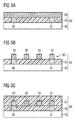
- FIGS 3A to 3F show an exemplary embodiment of a process for fabricating the capacitive sensor 11 of the sensor arrangement 10.
- the result of the process is a capacitive sensor 11 similar to the capacitive sensor shown in Figures 2A and 2B .
- the capacitive sensor 11 shown in Figures 1A, 1B , 2D , 4A to 4C can also be fabricated by the process illustrated in Figures 3A to 3F after some minor modifications.
- the process starts with the semiconductor body 60 having the semiconductor substrate 35.
- the semiconductor substrate 35 has the form of a wafer.
- the semiconductor substrate 35 is covered by the dielectric layer 33.
- the semiconductor substrate 35 may comprise an integrated circuit such as the readout circuit 50 shown in Figures 1B and 4C .
- the readout circuit 50 may be realized as a complementary metal oxide semiconductor circuit, abbreviated CMOS circuit.
- the semiconductor substrate 35 may comprise, not shown, at least a well and diffusion regions for source and drain regions of field-effect transistors.
- a metallization stack not shown, may be arranged between the dielectric layer 33 and the semiconductor substrate 35 .
- the metallization stack may comprise at least a metallization layers, e.g. made of polysilicon, a silicide or a metal, and at least a dielectric layer. The dielectric layer or layers separate the metallization layers from each other and from the semiconductor substrate 35.
- the dielectric layer 33 may be, for example, a silicon nitride or silicon dioxide layer.
- a metallization layer 82 is deposited on the dielectric layer 33.
- the metallization layer 82 may be called metal 1.
- the metallization layer 82 may be made out of aluminum, copper, tungsten, platinum or another metal. Vias 81, 81 are arranged between the metallization layer 82 and the semiconductor substrate 35 or a metallization layer of the not shown metallization stack.
- the metallization layer 82 is patterned.
- the third, the fourth and a further third electrode lines 20, 24, 21 are realized by etching the metallization layer 82.
- a contact line 83 is realized by etching of the metallization layer 82.
- the contact line 83 is arranged on top of the via 80.
- the further third electrode line 21 is in contact to the via 81.
- the further dielectric layer 34 is deposited.
- the further dielectric layer 34 may be called intermetal dielectric layer.
- the further dielectric layer 34 may be made of silicon nitride or silicon dioxide.
- the further dielectric layer 34 is deposited on the structures etched out of the metallization layer 82 and on the dielectric layer 33.
- a further metallization layer 85 is deposited on the further dielectric layer 34 and patterned.
- the further metallization layer 85 may be called metal 2.
- the deposition and the patterning of the further metallization layer 85 may be realized similar to the deposition and patterning of the metallization layer 82.
- the first, the second and a further first electrode lines 12, 16, 13 are realized by the further metallization layer 85.
- a connection line 86 is also made from the further metallization layer 85.
- the connection line 86 is arranged on top of a via 87 that is turn arranged on top of the contact line 83.
- the connection line 86 is electrically connected by the via 87, the contact line 83 and the via 80 to the semiconductor substrate 35 or to a metallization layer of the not shown metallization stack.
- an electric connection is realized from the first electrode lines 12 to 15 and/or the second electrode lines 16 to 19 made of the further metallization layer 85 to the semiconductor substrate 35 or to a metallization layer of the not shown metallization stack.
- the third electrode lines 20 to 23 or/and the fourth electrode lines 24 to 27 made of the metallization layer 82 are electrically connected by the via 81 to the semiconductor substrate 35 or to a metallization layer of the not shown metallization stack.
- the further dielectric layer 34 is patterned.
- the etching process of the further dielectric layer 34 stops at the top surface of the dielectric layer 33.
- the first to the fourth electrode lines 12 to 27 and the further dielectric layer 34 in the first and second stacks 70, 71 and in the further stacks are not removed.
- the sensitive layer 30 is deposited, e.g. by a spin-on process.
- the height h of the sensitive layer 30 is less than a stack height ts of one of the first and second stacks 70, 71.
- the sensitive layer 30 does not cover the top surface of the first and the second electrode lines 12, 16.
- the height h of the sensitive layer 30 may be larger than the stack height ts of the first stack 70.
- the capacitive sensor 11 may be fabricated via back-end processing.
- simultaneous processing of the top two metal layers 82, 85 is performed.
- two identical structures will be created in two different metal layers 82, 85.
- Two aligned electrode sets in two different metal layers 82, 85 may be fabricated by back-end processing as shown in Figures 3A to 3F .
- the gaps 36 which are also be called trenches may have an aspect ratio larger than two:
- the stack height ts of the first gap 36 may be larger than two times of the first width g1 of the first gap 36.
- the polymer 30 is deposited in such a manner that trenches are filled which have an aspect ratio larger than two. Electrode spacing can be adjusted to accommodate for polymer deposition.
- the capacitive sensor 11 is realized on an insulating substrate such as glass that replaces the dielectric layer 33 and the semiconductor substrate 35.
- the capacitive sensor 11 and the readout circuit 50 are realized on separate dies.
- FIG 4A shows a further exemplary embodiment of the capacitive sensor 11 of the sensor arrangement 10 that is a further development of the above-shown embodiments.
- the capacitive sensor 11 comprises the first, second and third electrode lines 12, 16, 20. Additionally, the capacitive sensor 11 comprises a further third electrode line 21.
- the third electrode line 20 is arranged between the first and the second electrode line 12, 16.
- the second electrode line 16 is arranged between the third and the further third electrode line 20, 21.
- the capacitive sensor 11 may be free of the fourth electrode line 24 or the fourth electrode lines 24 to 27.
- the four electrode lines 12, 20, 16, 21 shown in Figure 4A will be repeated.
- the four electrode lines 12, 20, 16, 21 of Figure 4A form an elementary cell which is periodically repeated.
- Either one of the first electrode lines 12 to 15 or one of the second electrode lines 16 to 19 is between two of the third electrode lines 20 to 23.
- the number of the third electrode lines 20 to 23 is approximately equal to the sum of the first and the second electrode lines 12 to 19.
- the sensitive layer 30 covers the first to the third electrode lines 12 to 23.
- Each of the first to the third electrode lines 12 to 23 is on the same plane.
- Each of the first to the third electrode lines 12 to 23 have the same distance d1 to the interface 31.
- Each of the first to the third electrode lines 12 to 23 is directly arranged on the dielectric layer 33.
- the third electrode line 20 and the further third electrode line 21 are kept floating.
- Electric field lines E3 are generated between the first and the second electrode line 12, 16. Due to the large distance g3 between the first and the second electrode line 12, 16, the electric field lines E3 have a high penetration depth inside the sensitive layer 30. The electric field lines E3 may be in contact with the interface 31. Thus, by the electric field lines E3, a change of a parameter of the sensitive layer 30 at the interface 31 can be detected.
- FIG 4B shows the capacitive sensor 11 illustrated by Figure 4A in the second phase B.
- electrical field lines E4 to E6 are generated between the first and the third electrode lines 12, 20, between the second and the further third electrode lines 16, 21 and between the second and the third electrode line 16, 20.
- the first and the second electrode lines 12, 16 may be coupled together. Due to the small distance g1 between the first and the third electrode line 12, 20, between the second and the third electrode line 16, 20 and between the second and the further third electrode line 16, 21, the electric field lines E4 to E6 have only a low penetration depth inside the sensitive layer 30. By the electric field lines E4 to E6 a change of a parameter in the bulk of the sensitive layer 30 can be measured.
- FIG 4C shows an exemplary embodiment of the sensor arrangement 10 that is a further development of the above-shown embodiments.
- the capacitive sensor 11 as shown in Figure 4C is a schematic top view on the capacitive sensor 11 illustrated by Figures 4A and 4B .
- the readout circuit 50 is similar as shown in Figure 1B .
- the cross-section shown in Figures 4A and 4B is marked with DD.
- the third electrode lines 20 to 23 are arranged between the first and the second electrode lines 12 to 14, 16, 17. Thus, between one line of the first electrode lines 12 to 14 and one line of the second electrode lines 16, 17, in each case one line of the third electrode lines 20 to 23 is arranged.
- a line of the first electrode lines 12 to 14 has a large distance g3 to the neighboring line of the second electrode lines 16 to 17.
- a line of the first and the second electrode lines 12 to 14, 16, 17 only has a short distance g1 to the neighboring line of the third electrode lines 20 to 23.
- the first electrode lines 12 to 14 may be directly and permanently connected to the first input 56 of the converter 51.
- the first changeover switch 55 has an input connected to the second electrode lines 16, 17, a first output connected to the first input 56 of the converter 51 and a second output connected to the second input 57 of the converter 51.
- the second changeover switch 57 has an input connected to the third electrode line 20 to 23 and a first output connected to the second input 58 of the converter 51. A second output of the second converter switch 57 is kept open.
- the switching arrangement 54 comprises a switch 90 coupling the third electrode lines 20 to 24 to the second input 58 of the converter 51.
- the second changeover switch 57 may be omitted.
- the first electrode lines 12 to 14 are permanently connected to the first input 56 of the converter 51.
- the second electrode lines 16, 17 are coupled to the second input 57 of the converter 51 via the first changeover switch 55, and the third electrode lines 20 to 23 are kept floating.
- the second electrode lines 16, 17 are coupled to the first input 56 of the converter 51 and the third electrode lines 20 to 23 are coupled to the second input 58 of the converter 51 via the first and the second changeover switch 55, 57.
- the capacitive sensor 11 has different electric field lines E3 to E6 in the first and the second phase A, B and, thus, different parameters of the sensitive layer 30 can be measured in the first and the second phase A, B.
- the first and the second measurement signals S1, S2 are determined and further processed such as described above and shown in Figure 1B .
- the sensor arrangement 10 of Figures 4A to 4C uses a consecutive set of lateral electrode lines which can be biased differently.
- the electrodes lines measure the material 30 close to the electrode lines.
- the effective spacing of the electrode lines is increased whereby the electric field lines E3 also probe the air-polymer interface 31.
- the capacitive sensor 11 provides a lateral electrode configuration with different biasing.
- the electrical field lines E3, E4, E5 probe different parts of the material 30.
- the material 30 close to the electrode lines is probed.
- the material 30 and the air-polymer interface 31 are probed.
- the read-out circuit 50 includes switches to polarize the same electrode sets by two different biasing schemes.
- the sensitive layer 30 has a smaller height h.
- the first distance d1 is set such that the electric field lines E3 in the first phase A extend to the ambient gas 32.
- the first distance d1 may be less than the first width g1 of the first gap 36 between two neighboring electrode lines 12, 16, 20, 21.
- the electrode lines 12, 16, 20, 21 may have the identical width w.
- Figures 5A to 5D show exemplary measurement results of a capacitive sensor 11 realized as an interdigitated capacitor.
- the interdigitated capacitor may have, for example, only first and second electrode lines.
- a measured off-set in capacitance and in Figures 5B and 5D a thickness of a polyimide film after several days of exposure to stress conditions (95% relative humidity, 95°C) and subsequent recovery treatment is shown.
- the amount of drift is different for different material properties.
- the sensor arrangement 10 exploits these differences to identify drift and trigger a warning or on-chip countermeasures, if possible.
- drift in relative humidity sensors after exposure to extreme conditions show that after 15 days of stress (95°C, 95% relative humidity), there is approximately 0.4 to 1.5% permanent expansion of the polymer and the polymer capacitance has changed approximately 0.2%.
- a recovery treatment regenerates the material 30 and partially removes drift.
Abstract
Description
- Sensor arrangement and method for generating measurement signals
- The present invention is related to a sensor arrangement and a method for generating measurement signals.
- The sensor arrangement is configured as a chemical sensor arrangement. Thus, the sensor arrangement is designed for the measurement of a parameter in a gas or a liquid. For example, the sensor arrangement may be realized for the detection of humidity, i.e. for the detection of water molecules in air.
- A capacitive sensor with a sensitive layer is often used for humidity detection. The humidity may change several parameters of the sensitive layer. However, only one parameter of the sensitive layer is commonly measured.
- It is an object of the invention to provide a sensor arrangement and a method for generating measurement signals which allow the measurement of more than one parameter of a sensitive layer.
- The object is solved by the independent claims. Further developments and embodiments are described in the dependent claims.
- In an embodiment, a sensor arrangement comprises a capacitive sensor and a readout circuit. The capacitive sensor comprises a first electrode line, a second electrode line, a third electrode line and a sensitive layer. The sensitive layer is arranged at the first, the second and the third electrode lines. The readout circuit comprises a capacitance-to-digital converter, abbreviated converter. The readout circuit is coupled to the first, the second and the third electrode lines. The readout circuit is configured to generate a first measurement signal using the first and the second electrode lines and to generate a second measurement signal using at least the third electrode line.
- Since the first, second and third electrode lines are arranged at the sensitive layer, more than one measurement signal can be generated and, thus, more than one parameter of the sensitive layer can be measured. Advantageously, the sensor arrangement allows more information to be gained out of the sensitive layer.
- In an embodiment, the sensitive layer is in contact with the first, the second and the third electrode lines.
- In an embodiment, the converter is coupled on its input side to the first, the second and the third electrode lines. The converter generates the first measurement signals and the second measurement signal.
- In an alternative embodiment, the converter is coupled on its input side to the first and the second electrode lines. The converter generates the first measurement signal. The readout circuit comprises a further capacitance-to-digital converter - abbreviated further converter - that is coupled at least to the third electrode line. The further converter generates the second measurement signal.
- In an embodiment, the sensor arrangement is realized as a chemical sensor arrangement. The chemical sensor arrangement may be implemented as a gas sensor arrangement. The gas sensor arrangement may be configured as a humidity sensor arrangement. Since water molecules are an example for a gas, a humidity sensor arrangement is an embodiment of a gas sensor arrangement.
- In an embodiment, the sensitive layer is designed to absorb a gas to be detected, such as CO2 or SO2. The sensitive layer may change its permittivity depending on the absorbed gas. The sensitive layer may change its capacitance and/or its resistance depending on the absorbed gas.
- In the case that the gas sensor arrangement is configured as a humidity sensor arrangement, the gas absorbed by sensitive layer are water molecules,
H 20. However, a humidity sensor often has a different behavior than a gas sensor for other gases, since water molecules are not burnable such as CO or hydrocarbons, have a high concentration and have an upper limit in air. - The sensitive layer may be a polymer. The sensitive layer may be made of a polyimide.
- In an embodiment, the first, the second and the third electrode lines are configured such that the first measurement signal depends more on a swelling of the sensitive layer than the second measurement signal. The swelling of the sensitive layer may occur, when the sensitive layer absorbs the gas to be detected, for example the water molecules.
- In an embodiment, the first measurement signal depends more on the changing thickness of the sensitive layer than the second measurement signal. The sensitive layer increases its thickness by the swelling.
- The swelling may be a reversible swelling, a permanent swelling or a swelling that is partially reversible and partially permanent. In the case of a reversible swelling, the thickness of the sensitive layer increases with rising concentration of the gas to be detected, e.g. humidity, and decreases with decreasing concentration of the gas to be detected, e.g. humidity. In the case of a permanent swelling, the thickness of the sensitive layer does not decrease, when the concentration of the gas to be detected, e.g. humidity, decreases.
- In an embodiment, the first, the second and the third electrode lines are configured such that the second measurement signal depends more on the bulk properties of the sensitive layer than the first measurement signal.
- In an embodiment, the readout circuit provides a gas signal as a function of the first measurement signal and the second measurement signal. Thus, both the first and the second measurement signals are used to determine the gas signal. The gas signal may be a humidity signal.
- The readout circuit may have a digital processor coupled to the converter. Alternatively, the digital processor of the readout circuit is coupled to the converter and the further converter. The digital processor may be implemented as a microcontroller, a microprocessor or a state machine. The readout circuit may comprises a memory coupled to the digital processor.
- The digital processor may calculate the gas signal.
- In an embodiment, the digital processor calculates the gas signal using an equation and/or a look-up table with the first and the second measurement signals as inputs.
- In an embodiment, the digital processor calculates a first gas signal using a first equation and/or a first look-up table with the first measurement signal as an input. Moreover, the digital processor calculates a second gas signal using a second equation and/or a second look-up table and using the second measurement signal as an input. The gas signal may be calculated by the digital processor as an average value of the first and the second gas signal.
- In an embodiment, the readout circuit provides a drift signal as a function of the first and the second measurement signal. The digital processor may perform the calculation of the drift signal. The digital processor may provide the drift signal as a function of the first and the second measurement signal and data stored in the memory.
- In an embodiment, the digital processor may calculate the drift signal using the first and the second gas signals as inputs. The drift signal has a value indicating a drift, when the first gas signal is different from the second gas signal. The value of the drift signal may be a function of the difference between the first and the second gas signal, e.g. may be proportional to said difference.
- In an embodiment, the readout circuit compares the first and the second measurement signal with correlation data stored in the memory. The readout circuit calculates the drift signal depending on the result of the comparison. If the first and the second measurement signal correlate to each other, the readout circuit may calculate a value of the drift signal indicating an absence of a drift. In case the first and the second measurement signal have only a small or none correlation, the readout circuit calculates the drift signal with a value indicating a drift.
- In an embodiment, the sensor arrangement performs an offset correction, generates a warning signal and/or starts a regeneration cycle depending on the value of the drift signal. The readout circuit may be configured to compare the value of the drift signal with a threshold value and to generate the warning signal, to start the regeneration cycle and/or to perform the offset correction in case the drift signal is higher than the threshold value. Alternatively, the readout circuit may perform an offset correction for each value of the drift signal that indicates a drift.
- In an embodiment, the capacitive sensor comprises a fourth electrode line. The sensitive layer is arranged at the fourth electrode line. The fourth electrode line is coupled to the readout circuit. The readout circuit is configured to generate the second measurement signal using the third and the fourth electrode lines. The converter may be coupled on its input side to the third and the fourth electrode lines.
- In case the readout circuit comprises the converter and the further converter, the further converter is coupled on its input side to the third and fourth electrode lines. The converter is coupled on its input side to the first and second electrode lines.
- In an embodiment, a distance of the first and second electrode lines to an interface between the sensitive layer and an ambient gas is less than a distance of the third and fourth electrode lines to said interface. Thus, the first to the fourth electrode lines may be arranged in different planes. Thus, a change of a parameter at the interface can be detected by the first and second electrode lines and changes the first measurement signal to a higher extent than the second measurement signal. A change in the bulk of the sensitive layer can be more easily detected by the third and fourth electrode lines and, thus, changes the second measurement signal to a higher extent than the first measurement signal.
- In an embodiment, the capacitive sensor comprises a semiconductor substrate and at least a dielectric layer on top of the semiconductor substrate. A distance of the first and second electrode lines to the semiconductor substrate is larger than a distance of the third and fourth electrode lines to the semiconductor substrate.
- The third and the fourth electrode lines may be covered by the sensitive layer. The third and fourth electrode lines may each have a top surface that is covered by the sensitive layer. The third and fourth electrode lines may have side surface that are covered by the sensitive layer.
- In an embodiment, the first and the second electrode lines are covered by the sensitive layer.
- In an alternative embodiment, the first and the second electrode lines are only partially covered by the sensitive layer. For example, the top surface of the first and the second electrode line may be free from the sensitive layer. For example, only a part of the side surfaces of the first and second electrode line may be in contact with the sensitive layer.
- In an embodiment, an interface of the sensitive layer and the ambient air is below the top surface and above a bottom surface of the first and second electrode lines. Optionally, said interface may be in the midst of the top surface and the bottom surface. Thus, said interface may be in the midst of the side surfaces of the first and second electrode lines.
- In an embodiment, the sensitive layer may not be perfectly flat. A thickness of the sensitive layer may be higher adjacent to the first and second electrode lines than in an area between the first and the second electrode lines. However, an average thickness of the sensitive layer and an average interface of the sensitive layer to the ambient air can be defined. Thus, an average interface of the sensitive layer to the ambient air is below the top surface and above the bottom surface of the first and second electrode lines.
- In an embodiment, the first, the second and the third electrode lines are arranged in a plane. A distance of the first, the second and the third electrode lines to a semiconductor substrate of the capacitive sensor is approximately identical.
- In an embodiment, a distance of the first electrode line to the second electrode line is larger than a distance of the first electrode line to the third electrode line. The readout circuit generates the first measurement signal by a capacitance measurement between the first and the second electrode line. Moreover, the readout circuit generates the second measurement signal by a capacitance measurement between the first and the third electrode line.
- In an embodiment, the first and the second electrode lines are coupled to the converter in a first phase and the first and the third electrode line are coupled to the converter in a second phase. Due to the small distance of the first electrode line to the third electrode line, the second measurement signal depends more on the bulk parameter of the sensitive layer than the first measurement signal. Due to the larger distance of the first electrode line to the second electrode line, the first measurement signal depends more on parameters at the surface of the sensitive layer than the second measurement signal.
- In an embodiment, the capacitive sensor comprises a transducer layout configured to track permanent material changes, such as permanent changes of the sensitive layer.
- The sensor arrangement may perform active cancellation of sensor drift.
- The sensor arrangement may track differences in capacitive readout due to material changes (i.e. swelling) and bulk dielectric constant changes, thus detecting and decoupling drift (or permanent capacitive change) from regular dielectric changes. Thus, the sensor arrangement is able to counteract a drift in the sensitive layer. Sensor drift can often be attributed to bulk effects of the sensitive layer that is also called material or gas sensitive layer.
- The sensor arrangement may use at least two material properties to determine the gas concentration or the relative humidity. As a result, the accuracy of the sensor read-out increases. The sensor arrangement may able to identify when a recovery treatment is required. Such a recovery treatment may return the material, e.g. the sensitive layer, to its original state.
- The sensor arrangement may include tracking whether permanent changes in the relative humidity sensitive bulk material occur. The sensor arrangement may include to identify drift to initiate countermeasures to these effects. The sensor arrangement simultaneously monitors multiple types of drift (permanent swelling and dielectric constant drift) in the gas sensitive material and determines the conditions for initiating countermeasures. The sensor arrangement identifies drift and triggers a warning or on-chip countermeasures.
- The sensor arrangement may be designed to track two different material properties by two capacitive measurements. This is realized by adjusting the transducer layout (including different electrode sets) or/and by applying different electrode polarization on the same electrode set.
- The sensor arrangement may be designed to identify drift. The two capacitive measurements are compared continuously. Ideally, a correlation plot or correlation data between relative humidity - (reversible) swelling - (reversible) dielectric constant exists. If irreversible swelling occurs, the dimensional material changes will not correspond any more with dielectric constant changes according to the pre-drift correlation. The double capacitive measurement of the sensor arrangement identifies the deviation from this correlation.
- The sensitive layer may be a polymer material or out of other material classes such as metal-organic frameworks, abbreviated MOF, or ionic liquids. The sensitive layer may be designed for capacitive measurement or capacitive gas sensing.
- In an embodiment, the sensor arrangement independently obtains information from the polymer thickness and the polymer bulk dielectric constant. To achieve this with a capacitive measurement, the thickness of the polymer and the spacing of the electrode lines are carefully matched. The capacitive thickness measurement makes use of electric field lines that extend beyond the air-polymer interface. For example, the distance between the electrodes lines and the polymer-air interface should be less than three times the spacing of the electrode lines (rule of thumb). The opposite is true for the electrodes lines measuring the polymer dielectric properties: The distance to the air-polymer interface should be further than three times the spacing of the electrode lines.
- In an embodiment, the sensor arrangement may track permanent material changes via the use of two different sets of electrodes lines (with different distances to the air/polymer interface) or/and via changing the electrode configuration. Polymer swelling and especially permanent polymer swelling typically only displaces the air/polymer interface by a very small amount, typically a few nanometer. An electrode configuration which is not fully covered by the polymer is more sensitive to detect this change in comparison to an electrode configuration which is fully covered by the polymer. Therefore, the air/polymer interface may be placed in the most sensitive part of the electrode configuration, e.g. halfway the electrode height. Thus, the sensor arrangement may be able to detect any (permanent) swelling of the polymer layer.
- In an embodiment, a method for generating measurement signals comprises generating a first measurement signal using a first and a second electrode line of a capacitive sensor by a readout circuit. Moreover, a second measurement signal is generated using at least a third electrode line of the capacitive sensor by the readout circuit. The capacitive sensor comprises a sensitive layer that is arranged at the first, second and third electrode lines. The readout circuit comprises a capacitance-to-digital converter.
- Advantageously, by using three different electrode lines in combination with one sensitive layer, different parameters of the sensitive layer can be detected by the readout circuit.
- The following description of figures of exemplary embodiments may further illustrate and explain the invention. Elements, layers and circuit blocks with the same structure and the same effect, respectively, appear with equivalent reference symbols. In so far as elements, layers and circuit blocks correspond to one another in terms of their function in different figures, the description thereof is not repeated for each of the following figures.
- Figures 1A and 1B
- show an exemplary embodiment of a sensor arrangement with a capacitive sensor;
- Figures 2A to 2D
- show further exemplary embodiments of a capacitive sensor;
- Figures 3A to 3F
- show an exemplary process for fabrication of a capacitive sensor;
- Figures 4A to 4C
- show a further exemplary embodiment of a sensor arrangement; and
- Figures 5A to 5D
- show exemplary measurements of a capacitive sensor.
-
Figure 1A shows an exemplary embodiment of acapacitive sensor 11 of asensor arrangement 10. Thecapacitive sensor 11 comprises afirst electrode line 12, asecond electrode line 16 and athird electrode line 20. Moreover, thecapacitive sensor 11 comprises afourth electrode line 24. Thecapacitive sensor 11 comprises asensitive layer 30. Thesensitive layer 30 has aninterface 31 to anambient gas 32. Theambient gas 32 comprises the parameter to be detected, such as water molecules or another target gas. Thesensitive layer 30 may be a polymer, such as a polyimide. - The first and the
second electrode line interface 31 between thesensitive layer 30 and theambient gas 32. Similarly, the third and thefourth electrode line interface 31. The second distance d2 is larger than the first distance d1. In an example, the first distance d1 may have a value of 1 µm and the second distance d2 may have a value of 4 µm. The first andsecond electrode lines fourth electrode lines - A
first gap 36 between the first and thesecond electrode line second gap 37 between the third and thefourth electrode line electrode lines - The
capacitive sensor 11 comprises adielectric layer 33. The first to thefourth electrode lines dielectric layer 30. The third and thefourth electrode lines dielectric layer 33. Thecapacitive sensor 11 comprises afurther dielectric layer 34 that is arranged between thedielectric layer 33 and the first and thesecond electrode lines - The
sensitive layer 30 covers the top surface of the third and thefourth electrode lines sensitive layer 16 also covers the side surfaces of the third and thefourth electrode lines sensitive layer 16 covers the top surfaces of the first and thesecond electrode lines sensitive layer 30 also covers the side surfaces of the first and thesecond electrode lines sensitive layer 30 fills the first and thesecond gap - Additionally, the
capacitive sensor 11 comprises asemiconductor substrate 35 on which thedielectric layer 33 is arranged. Thus, thecapacitive sensor 11 comprises a first stack comprising thethird electrode line 20, thedielectric layer 19 and thesemiconductor substrate 21. Additionally, thecapacitor sensor 11 comprises a second stack comprising thefirst electrode line 12, thefurther dielectric layer 34, thedielectric layer 33 and thesemiconductor substrate 35. Thedielectric layer 33 and/or thefurther dielectric layer 34 may be realized as inter-metal dielectric layers. - Electric field lines E1 run from the
first electrode line 12 to thesecond electrode line 16 and are generated by applying different voltages to the first and thesecond electrode lines sensitive layer 30 but also extend through theambient gas 32. Thus, some of the electric field lines E1 cross theinterface 31. Electric field lines E2 extend from the third to thefourth electrode line sensitive layer 30. The electric field lines E2 do not touch theinterface 31 or theambient gas 32. - The
first electrode line 12 is free of an electric conductive connection to thesecond electrode line 16. Thethird electrode line 20 is free of an electric conductive connection to thefourth electrode line 24. The first and thesecond electrode lines fourth electrode lines second electrode lines fourth electrode lines fourth electrode lines - In
Figure 1A , a cross-section of thecapacitive sensor 11 is shown. In thecapacitive sensor 11, a first electrode set 12, 16 is dedicated to track permanent dimensional changes and a second separate electrode set 20, 24 is dedicated to track dielectric constant changes. The first electrode set 12, 16 is physically located closer to the air-polymer interface 31 than the second electrode set 20, 24 to capture dimensional effects. Thecapacitive sensor 11 tracks dimensional changes in thepolyimide 30 using two different electrode pairs. The polyimide-air interface 31 moves in the fringe field of the first electrode set 12, 16, also called first electrode pair. - Optionally, the first width g1 and the first distance d1 are set according to the following equation:

- Optionally, the second width g2 and the second distance d2 are set according to the following equation:

- In an alternative embodiment, not shown, the
sensitive layer 30 only covers a part of the side surfaces of the first and thesecond electrode lines second electrode lines - In an alternative embodiment, not shown, a metallization stack may be arranged between the
semiconductor substrate 35 and thedielectric layer 33. The metallization stack may comprise at least one further metallization layer and one further dielectric layer. -
Figure 1B shows an exemplary embodiment of thesensor arrangement 10 comprising thecapacitive sensor 11.Figure 1A shows the cross-section of a part of thecapacitive sensor 11 marked with EE inFigure 1B . Thefirst electrode line 12 is electrically connected to furtherfirst electrode lines 13 to 15 of thecapacitive sensor 11. Thefirst electrode line 12 and the furtherfirst electrode lines 13 to 15 run parallel to each other. Thefirst electrode line 12 and the furtherfirst electrode lines 13 to 15 form a firstinterdigitated electrode 40. - Correspondingly, the
second electrode line 16 is electrically connected to furthersecond electrode lines 17 to 19 of thecapacitive sensor 11. Thesecond electrode line 16 and the furthersecond electrode lines 17 to 19 run parallel to each other. Thesecond electrode line 16 and the furthersecond electrode lines 17 to 19 form a secondinterdigitated electrode 41. The first and the secondinterdigitated electrode interdigitated capacitor 42. - Moreover, the
capacitive sensor 11 comprises furtherthird electrode lines 21 to 23 that are electrically connected to thethird electrode line 20. Thethird electrode line 20 and the furtherthird electrode lines 21 to 23 run parallel to each other. Thethird electrode line 20 and the furtherthird electrode lines 21 to 23 form a thirdinterdigitated electrode 43. - Correspondingly, the
fourth electrode line 24 is electrically connected to furtherfourth electrode lines 25 to 27 of thecapacitive sensor 11. Thefourth electrode line 24 and the furtherfourth electrode lines 25 to 27 run parallel to each other. Thefourth electrode line 24 and the furtherfourth electrode lines 25 to 27 form a fourthinterdigitated electrode 44. The third and the fourthinterdigitated electrode interdigitated capacitor 45. - The
first electrode line 12 and the furtherfirst electrode lines 13 to 15 are abbreviated asfirst electrode lines 12 to 15 in the following text. Correspondingly,second electrode lines 16 to 19,third electrode lines 20 to 23 andfourth electrode lines 24 to 27 are defined. - The
sensor arrangement 10 comprises areadout circuit 50 that is electrically coupled to thefirst electrode lines 12 to 15, thesecond electrode lines 16 to 19, thethird electrode lines 20 to 23 and thefourth electrode lines 24 to 27. - The
readout circuit 50 comprises a capacitance-to-digital converter 51, abbreviated converter. Theconverter 51 is electrically coupled to the first, second, third andfourth electrode lines 12 to 27. Moreover, thereadout circuit 50 comprises adigital processor 52 that is coupled on its input side to theconverter 51. Thereadout circuit 50 comprises amemory 53 that is coupled to thedigital processor 52. - Furthermore, the
readout circuit 50 comprises a switchingarrangement 54. A control input of the switchingarrangement 54 is coupled to an output of thedigital processor 52. The switchingarrangement 54 comprises afirst changeover switch 55 having a first input connected to thefirst electrode lines 12 to 15 and a second input connected to thethird electrode lines 20 to 23 and an output connected to afirst input 56 of theconverter 51. The switchingarrangement 54 may comprise asecond changeover switch 57 with a first input connected to thesecond electrode lines 16 to 19, a second input connected to thefourth electrode lines 24 to 27 and an output connected to asecond input 58 of theconverter 51. - The
sensor arrangement 10 comprises asemiconductor body 60. Thecapacitive sensor 11 and thereadout circuit 50 are part of thesemiconductor body 60. Thus, thesemiconductor substrate 35, shown inFigure 1A , is used for the realization of thereadout circuit 50. - In a first phase A, the
first electrode lines 12 to 15 are coupled to thefirst input 56 of theconverter 51 via thefirst changeover switch 55. Thesecond electrode lines 16 to 19 are electrically coupled via thesecond changeover switch 57 to thesecond input 58 of theconverter 51. Theconverter 51 generates a firstmeasurement signal S 1. Thus, the first measurement signal S1 is generated using the first and thesecond electrode lines 12 to 19. The first measurement signal S1 is a function of the capacitance between thefirst electrode lines 12 to 15 and thesecond electrode lines 16 to 19. - In a second phase B, the
third electrode lines 20 to 23 are coupled via thefirst changeover switch 55 to thefirst input 56 of theconverter 51. Thefourth electrode lines 24 to 27 are coupled via thesecond changeover switch 57 to thesecond input 58 of theconverter 51. Theconverter 51 generates a second measurement signal S2. Thus, the second measurement signal S2 is generated using the third and thefourth electrode lines 20 to 27. The second measurement signal S2 is a function of the capacitance between thethird electrode lines 20 to 23 and thefourth electrode lines 24 to 27. The first and the second measurement signals S1, S2 are provided to thedigital processor 52. - The
digital processor 52 generates a gas signal SG at a first output 61. The gas signal SG may be realized as humidity signal. The humidity signal provides the information about the relative humidity in theambient gas 32. The gas signal SG may be determined by thedigital processor 52 using the first and the second measurement signals S1, S2. Moreover, thedigital processor 52 generates a drift signal SD at asecond output 62. The drift signal SD may be determined by thedigital processor 52 using the first and the second measurement signals S1, S2. - The
digital processor 52 uses data stored in thememory 53 for providing the gas signal SG and the drift signal SD. Thememory 53 may store parameters of functions or a look-up table which are used for the calculation of the gas signal SG and the drift signal SD using the first and the second measurement signal S1, S2 as inputs. The parameter of the functions or the look-up table may be stored in a non-volatile block of thememory 53 such as an electrically erasable programmable read only memory, abbreviated EEPROM, or a one-time programmable memory, abbreviated OTP. - The first and the second measurement signal S1, S2 are alternatively generated. Since the first and the second measurement signal S1, S2 are generated in separate phases, namely the first and the second phase A, B, they are generated at separate points of time and the
digital processor 52 may store intermediate values in a volatile block of thememory 53. The first and the second phase A, B are periodically repeated. - The
sensor arrangement 10 identifies the drift by comparing the gas measurement to a prior stored gas correlation plot or the relative humidity measurement to a prior stored relative humidity correlation plot. - In order to detect permanent swelling off-sets, the ratio of both measured values is known for "normal" - reversible conditions (determined by the correlation curve before drift). For each dielectric constant value, a fixed amount of swelling is expected. Permanent changes are detected when the ratio Δh/Δε deviates from the calibrated values. The
sensor arrangement 10 applies a compensation which could be an off-set correction, a warning signal from thesensor arrangement 10 and/or a regeneration cycle. - The first measurement signal S1 is mainly a function of the height h and of the dielectric constant ε of the
sensitive layer 30 and the second measurement signal S2 is mainly a function of the dielectric constant ε of thesensitive layer 30. Both the height h and the dielectric constant ε depend on the gas concentration to be measured or, in case of humidity sensing, on the relative humidity in theambient gas 32. In an example, the drift signal SD may indicate the absence of a drift, when a predetermined value of the second measurement signal S2 can be measured at a measured value of the first measurement signal S1. When at the measured value of the first measurement signal S1, the predetermined value of the second measurement signal S2 differs from the actual measured value of the second measurement signal S2, than the drift signal SD may indicate a drift. - In an alternative embodiment, not shown, the output of the
second changeover switch 57 is connected to a reference potential terminal. - In an alternative embodiment, not shown, the second and the
fourth electrode lines 16 to 19, 24 to 27 are directly connected to a reference potential terminal. Thesecond changeover switch 57 is omitted. -
Figure 2A shows a further exemplary embodiment of thecapacitive sensor 11 of thesensor arrangement 10 which is a further development of the embodiments shown inFigures 1A and 1B . Thefirst electrode line 12 is arranged on top of thethird electrode line 20. Correspondingly, thesecond electrode line 16 is arranged on top of thefourth electrode line 24. Thefurther dielectric layer 34 is arranged between the first and thethird electrode lines fourth electrode lines further dielectric layer 34 has a layer thickness t3. - In
Figure 2A , a cross-section is shown. The first to thefourth electrode lines capacitive sensor 11 comprises afirst stack 70 comprising thefirst electrode line 12, thefurther dielectric layer 34, thethird electrode line 20, thedielectric layer 33 and thesemiconductor substrate 35. Correspondingly, thecapacitive sensor 11 comprises asecond stack 71 comprising thesecond electrode line 16, thefurther dielectric layer 34, thefourth electrode line 24, thedielectric layer 33 and thesemiconductor substrate 35. - Contrary to
Figure 1A , the first and thesecond electrode lines sensitive layer 30. Thus, the top surfaces of the first and thesecond electrode lines sensitive layer 30. Thesensitive layer 30 only covers a part of the side surfaces of the first and thesecond electrode lines interface 31 is at the height of the side surfaces of the first and thesecond electrode lines - The
capacitive sensor 11 may comprise the furtherfirst electrode lines 13 to 15, the furthersecond electrode lines 17 to 19, the furtherthird electrode lines 21 to 23 and the furtherfourth electrode lines 25 to 27 that are connected to the first, second, third andfourth electrode lines interdigitated capacitor 45 is realized between the firstinterdigitated capacitor 42 and thedielectric layer 33. The firstinterdigitated capacitor 42 is realized on top of the secondinterdigitated capacitor 45. The first and the secondinterdigitated capacitors further dielectric layer 34. - Advantageously, an area for the realization of the
capacitive sensor 11 is reduced in comparison to the embodiment shown inFigure 1A . Thecapacitive sensor 11 realizes a vertical integration of theelectrode lines 12 to 27. The two separate electrode sets are vertically implemented in thecapacitive sensor 11. Thecapacitive sensor 11 aims for a high sensitivity to dimensional changes. -
Figure 2B shows thecapacitive sensor 11 as illustrated inFigure 2A in the first and the second phase A, B. In the first phase A shown on the left side ofFigure 2B , thereadout circuit 50 provides a driving signal S to thefirst electrode line 12 and a reference potential G to thesecond electrode line 16. Thesecond electrode line 16 is grounded. Thefirst electrode line 12 is marked with an S and thesecond electrode line 16 is marked with a G. Moreover, the third and thefourth electrode lines fourth electrode lines Figure 2B , thecapacitive sensor 11 is shown in the second phase B. In the second phase B, the first and thesecond electrodes readout circuit 50 applies the driving signal S to thethird electrode 20 and the reference potential G to thefourth electrode 24. -
Figure 2C shows an exemplary embodiment of simulated results of thecapacitive sensor 11 shown inFigures 2A and 2B . Thesimulation curve 72 shows the sensitivity to the height h of thesensitive layer 30 versus the sensitivity to the dielectric constant ε using the first and thesecond electrode line second simulation curve 73 shows the sensitivity to the height h versus the sensitivity to the dielectric constant ε of the third and thefourth electrode lines fourth electrode lines sensitive layer 30, whereas the first and thesecond electrode lines sensitive layer 30. - The feasibility of the
capacitive sensor 11 was investigated with finite element simulation. The model parameters were taken to mimic the transducer dimensions for both the swelling (top electrode pair 40, 41) and dielectric (electrode pair Figures 2A and 2B . For this case, the polymer thickness h is chosen to obtain a maximum sensitivity of thetop electrode pair - The calculated capacitive changes are shown in
Figure 2C : The sensitivity of the two different electrode sets, namely the top and the buried electrode pair to swelling of the polymer in fF per nm compared to dielectric constant sensitivity is shown. The capacitance of thetop electrode lines electrode lines digital converter 51 is considered large enough for detecting sub-nm thickness changes to a significant level. The sensitivity to swelling is smaller for fully coveredtop electrodes lines - The following model parameters were used for finite element calculation: Width w and height t1, t2 of the electrode lines: 0.5 µ · 1.0 µm; electrode spacing: 1.0 µm horizontal, 1.0 µm vertical; polyimide height h: varying, nominal position halfway the first electrode layer (that is the middle of the side surface of the first electrode line 12). The task of the simulation was to solve for sensitivity to changes in the polyimide height hPI: δC/δhPI in [fF/nm] and changes in the dielectric constant ε: δC/δεPI for both top and second (buried) electrode configuration.
-
Figure 2D shows a further exemplary embodiment of thecapacitive sensor 11 that is a further development of the embodiments shown inFigures 1A, 1B ,2A and 2B . Similar toFigure 2A , thefirst electrode line 12 is arranged above thethird electrode line 20, wherein thefurther dielectric layer 34 separates the first and thethird electrode lines second electrode line 16 is arranged above thefourth electrode line 24, whereas thefurther dielectric layer 34 separates the second and thefourth electrode lines - The
capacitive sensor 11 comprises a firstdielectric layer stack 74 that is arranged on one side of thefirst stack 70. Thus, only one side surface of thefirst electrode line 12 and one side surface of thethird electrode line 20 are covered by the firstdielectric layer stack 74. Correspondingly, thecapacitive sensor 11 comprises a seconddielectric layer stack 75 that is arranged at the third and thefourth electrode lines third electrode line 16 and one side surface of thefourth electrode line 24 are covered by the seconddielectric layer stack 75. The first and the seconddielectric layer stack further dielectric layer 34 and anadditional dielectric layer 76. - The
first gap 36 between the first and thesecond stack sensitive layer 30. Thesensitive layer 30 in thefirst gap 36 is in direct contact with the side surfaces of the first, second, third andfourth electrode lines second electrode lines sensitive layer 30 has the first distance d1 between the top surfaces of the first and thesecond electrode lines interface 31. The first distance d1 may be in an interval of 0.1 µm to 5 µm or from 0.2 µm to 2 µm. For example, the first distance d1 is 1 µm. - The
capacitive sensor 11 may perform a residual passivation and may be suitable for a less ideal polymer deposition. - In an alternative embodiment, not shown, the top surfaces of the first and the
second electrode lines sensitive layer 30. Thesensitive layer 30 may have a height as shown inFigures 2A and 2B . -
Figures 3A to 3F show an exemplary embodiment of a process for fabricating thecapacitive sensor 11 of thesensor arrangement 10. The result of the process is acapacitive sensor 11 similar to the capacitive sensor shown inFigures 2A and 2B . However, also thecapacitive sensor 11 shown inFigures 1A, 1B ,2D ,4A to 4C can also be fabricated by the process illustrated inFigures 3A to 3F after some minor modifications. - As shown in
Figure 3A , the process starts with thesemiconductor body 60 having thesemiconductor substrate 35. Thesemiconductor substrate 35 has the form of a wafer. Thesemiconductor substrate 35 is covered by thedielectric layer 33. Thesemiconductor substrate 35 may comprise an integrated circuit such as thereadout circuit 50 shown inFigures 1B and4C . Thereadout circuit 50 may be realized as a complementary metal oxide semiconductor circuit, abbreviated CMOS circuit. Thus, thesemiconductor substrate 35 may comprise, not shown, at least a well and diffusion regions for source and drain regions of field-effect transistors. Between thedielectric layer 33 and the semiconductor substrate 35 a metallization stack, not shown, may be arranged. The metallization stack may comprise at least a metallization layers, e.g. made of polysilicon, a silicide or a metal, and at least a dielectric layer. The dielectric layer or layers separate the metallization layers from each other and from thesemiconductor substrate 35. - The
dielectric layer 33 may be, for example, a silicon nitride or silicon dioxide layer. Ametallization layer 82 is deposited on thedielectric layer 33. Themetallization layer 82 may be calledmetal 1. Themetallization layer 82 may be made out of aluminum, copper, tungsten, platinum or another metal.Vias metallization layer 82 and thesemiconductor substrate 35 or a metallization layer of the not shown metallization stack. - As shown in
Figure 3B , themetallization layer 82 is patterned. The third, the fourth and a furtherthird electrode lines metallization layer 82. Moreover, acontact line 83 is realized by etching of themetallization layer 82. Thecontact line 83 is arranged on top of the via 80. The furtherthird electrode line 21 is in contact to the via 81. - As illustrated in
Figure 3C , thefurther dielectric layer 34 is deposited. Thefurther dielectric layer 34 may be called intermetal dielectric layer. Thefurther dielectric layer 34 may be made of silicon nitride or silicon dioxide. Thefurther dielectric layer 34 is deposited on the structures etched out of themetallization layer 82 and on thedielectric layer 33. - As shown in
Figure 3D , a further metallization layer 85 is deposited on thefurther dielectric layer 34 and patterned. The further metallization layer 85 may be calledmetal 2. The deposition and the patterning of the further metallization layer 85 may be realized similar to the deposition and patterning of themetallization layer 82. Thus, the first, the second and a furtherfirst electrode lines connection line 86 is also made from the further metallization layer 85. Theconnection line 86 is arranged on top of a via 87 that is turn arranged on top of thecontact line 83. Thus, theconnection line 86 is electrically connected by the via 87, thecontact line 83 and the via 80 to thesemiconductor substrate 35 or to a metallization layer of the not shown metallization stack. - Thus, an electric connection is realized from the
first electrode lines 12 to 15 and/or thesecond electrode lines 16 to 19 made of the further metallization layer 85 to thesemiconductor substrate 35 or to a metallization layer of the not shown metallization stack. Thethird electrode lines 20 to 23 or/and thefourth electrode lines 24 to 27 made of themetallization layer 82 are electrically connected by the via 81 to thesemiconductor substrate 35 or to a metallization layer of the not shown metallization stack. - As illustrated in
Figure 3E , thefurther dielectric layer 34 is patterned. The etching process of thefurther dielectric layer 34 stops at the top surface of thedielectric layer 33. Moreover, the first to thefourth electrode lines 12 to 27 and thefurther dielectric layer 34 in the first andsecond stacks - As illustrated in
Figure 3F , thesensitive layer 30 is deposited, e.g. by a spin-on process. The height h of thesensitive layer 30 is less than a stack height ts of one of the first andsecond stacks sensitive layer 30 does not cover the top surface of the first and thesecond electrode lines - Alternatively, the height h of the
sensitive layer 30 may be larger than the stack height ts of thefirst stack 70. There may be amargin 84 in final polymer thickness, indicated by thebroken line 84 in the polymer deposition step inFigure 3F . - The
capacitive sensor 11 may be fabricated via back-end processing. In order to fabricate thecapacitive sensor 11 shown in the above mentioned figures, simultaneous processing of the top twometal layers 82, 85 is performed. In the example, two identical structures will be created in twodifferent metal layers 82, 85. Two aligned electrode sets in twodifferent metal layers 82, 85 may be fabricated by back-end processing as shown inFigures 3A to 3F . - The
gaps 36 which are also be called trenches may have an aspect ratio larger than two: The stack height ts of thefirst gap 36 may be larger than two times of the first width g1 of thefirst gap 36. Thepolymer 30 is deposited in such a manner that trenches are filled which have an aspect ratio larger than two. Electrode spacing can be adjusted to accommodate for polymer deposition. - In an alternative embodiment, not shown, the
capacitive sensor 11 is realized on an insulating substrate such as glass that replaces thedielectric layer 33 and thesemiconductor substrate 35. Thecapacitive sensor 11 and thereadout circuit 50 are realized on separate dies. -
Figure 4A shows a further exemplary embodiment of thecapacitive sensor 11 of thesensor arrangement 10 that is a further development of the above-shown embodiments. Thecapacitive sensor 11 comprises the first, second andthird electrode lines capacitive sensor 11 comprises a furtherthird electrode line 21. Thethird electrode line 20 is arranged between the first and thesecond electrode line second electrode line 16 is arranged between the third and the furtherthird electrode line capacitive sensor 11 may be free of thefourth electrode line 24 or thefourth electrode lines 24 to 27. - In a not shown embodiment, the four
electrode lines Figure 4A will be repeated. The fourelectrode lines Figure 4A form an elementary cell which is periodically repeated. Either one of thefirst electrode lines 12 to 15 or one of thesecond electrode lines 16 to 19 is between two of thethird electrode lines 20 to 23. The number of thethird electrode lines 20 to 23 is approximately equal to the sum of the first and thesecond electrode lines 12 to 19. - The
sensitive layer 30 covers the first to thethird electrode lines 12 to 23. Each of the first to thethird electrode lines 12 to 23 is on the same plane. Each of the first to thethird electrode lines 12 to 23 have the same distance d1 to theinterface 31. Each of the first to thethird electrode lines 12 to 23 is directly arranged on thedielectric layer 33. - In the first phase A, the
third electrode line 20 and the furtherthird electrode line 21 are kept floating. Electric field lines E3 are generated between the first and thesecond electrode line second electrode line sensitive layer 30. The electric field lines E3 may be in contact with theinterface 31. Thus, by the electric field lines E3, a change of a parameter of thesensitive layer 30 at theinterface 31 can be detected. -
Figure 4B shows thecapacitive sensor 11 illustrated byFigure 4A in the second phase B. In the second phase B, electrical field lines E4 to E6 are generated between the first and thethird electrode lines third electrode lines third electrode line second electrode lines third electrode line third electrode line third electrode line sensitive layer 30. By the electric field lines E4 to E6 a change of a parameter in the bulk of thesensitive layer 30 can be measured. -
Figure 4C shows an exemplary embodiment of thesensor arrangement 10 that is a further development of the above-shown embodiments. Thecapacitive sensor 11 as shown inFigure 4C is a schematic top view on thecapacitive sensor 11 illustrated byFigures 4A and 4B . Thereadout circuit 50 is similar as shown inFigure 1B . InFigure 4C , the cross-section shown inFigures 4A and 4B is marked with DD. Thethird electrode lines 20 to 23 are arranged between the first and thesecond electrode lines 12 to 14, 16, 17. Thus, between one line of thefirst electrode lines 12 to 14 and one line of thesecond electrode lines third electrode lines 20 to 23 is arranged. A line of thefirst electrode lines 12 to 14 has a large distance g3 to the neighboring line of thesecond electrode lines 16 to 17. A line of the first and thesecond electrode lines 12 to 14, 16, 17 only has a short distance g1 to the neighboring line of thethird electrode lines 20 to 23. - The
first electrode lines 12 to 14 may be directly and permanently connected to thefirst input 56 of theconverter 51. Thefirst changeover switch 55 has an input connected to thesecond electrode lines first input 56 of theconverter 51 and a second output connected to thesecond input 57 of theconverter 51. Thesecond changeover switch 57 has an input connected to thethird electrode line 20 to 23 and a first output connected to thesecond input 58 of theconverter 51. A second output of thesecond converter switch 57 is kept open. - Alternatively, the switching
arrangement 54 comprises a switch 90 coupling thethird electrode lines 20 to 24 to thesecond input 58 of theconverter 51. Thesecond changeover switch 57 may be omitted. - In the first and the second phase A, B, the
first electrode lines 12 to 14 are permanently connected to thefirst input 56 of theconverter 51. In the first phase A, thesecond electrode lines second input 57 of theconverter 51 via thefirst changeover switch 55, and thethird electrode lines 20 to 23 are kept floating. In the second phase B, thesecond electrode lines first input 56 of theconverter 51 and thethird electrode lines 20 to 23 are coupled to thesecond input 58 of theconverter 51 via the first and thesecond changeover switch - Advantageously, the
capacitive sensor 11 has different electric field lines E3 to E6 in the first and the second phase A, B and, thus, different parameters of thesensitive layer 30 can be measured in the first and the second phase A, B. The first and the second measurement signals S1, S2 are determined and further processed such as described above and shown inFigure 1B . - The
sensor arrangement 10 ofFigures 4A to 4C uses a consecutive set of lateral electrode lines which can be biased differently. During bias in the second phase B, the electrodes lines measure the material 30 close to the electrode lines. When changing the bias in the transition from the second phase B to the first phase A, the effective spacing of the electrode lines is increased whereby the electric field lines E3 also probe the air-polymer interface 31. - The
capacitive sensor 11 provides a lateral electrode configuration with different biasing. The electrical field lines E3, E4, E5 probe different parts of thematerial 30. In the second phase B, thematerial 30 close to the electrode lines is probed. In the first phase A, thematerial 30 and the air-polymer interface 31 are probed. The read-out circuit 50 includes switches to polarize the same electrode sets by two different biasing schemes. - In an alternative embodiment, not shown, the
sensitive layer 30 has a smaller height h. The first distance d1 is set such that the electric field lines E3 in the first phase A extend to theambient gas 32. The first distance d1 may be less than the first width g1 of thefirst gap 36 between two neighboringelectrode lines electrode lines -
Figures 5A to 5D show exemplary measurement results of acapacitive sensor 11 realized as an interdigitated capacitor. The interdigitated capacitor may have, for example, only first and second electrode lines. InFigures 5A and5C , a measured off-set in capacitance and inFigures 5B and5D , a thickness of a polyimide film after several days of exposure to stress conditions (95% relative humidity, 95°C) and subsequent recovery treatment is shown. As shown inFigures 5A to 5D , the amount of drift is different for different material properties. Thesensor arrangement 10 exploits these differences to identify drift and trigger a warning or on-chip countermeasures, if possible. - Some examples of drift in relative humidity sensors after exposure to extreme conditions show that after 15 days of stress (95°C, 95% relative humidity), there is approximately 0.4 to 1.5% permanent expansion of the polymer and the polymer capacitance has changed approximately 0.2%. Advantageously, a recovery treatment regenerates the
material 30 and partially removes drift. -
- 10
- sensor arrangement
- 11
- capacitive sensor
- 12
- first electrode line
- 13 to 15
- further first electrode line
- 16
- second electrode line
- 17 to 19
- further second electrode line
- 20
- third electrode line
- 21 to 23
- further third electrode line
- 24
- fourth electrode line
- 25 to 27
- further fourth electrode line
- 30
- sensitive layer
- 31
- interface
- 32
- ambient gas
- 33
- dielectric layer
- 34
- further dielectric layer
- 35
- semiconductor substrate
- 36, 37
- gap
- 40
- first interdigitated electrode
- 41
- second interdigitated electrode
- 42
- first interdigitated capacitor
- 43
- third interdigitated electrode
- 44
- fourth interdigitated electrode
- 45
- second interdigitated capacitor
- 50
- readout circuit
- 51
- capacitance-to-digital converter
- 52
- digital processor
- 53
- memory
- 54
- switching arrangement
- 55
- first changeover switch
- 56
- first input
- 57
- second changeover switch
- 58
- second input
- 60
- semiconductor body
- 61, 62
- output
- 70
- first stack
- 71
- second stack
- 72
- first simulation curve
- 73
- second simulation curve
- 74
- first dielectric layer stack
- 75
- second dielectric layer stack
- 76
- additional dielectric layer
- 80, 81
- via
- 82
- metallization layer
- 83
- contact line
- 84
- margin
- 85
- further metallization layer
- 86
- connection line
- 87
- further via
- A
- first phase
- B
- second phase
- d1, d2
- distance
- E1 to E6
- electric field lines
- g1, g2, w
- width
- g3
- distance
- SD
- drift signal
- SG
- gas signal
- S1
- first measurement signal
- S2
- second measurement signal
- t1, t2, t3
- thickness
- ts
- stack height
Claims (15)
- Sensor arrangement, comprising- a capacitive sensor (11) with a first electrode line (12), a second electrode line (16) and a third electrode line (20) and a sensitive layer (30) arranged at the first, the second and the third electrode line (12, 16, 20),- a readout circuit (50) that comprises a capacitance-to-digital converter (51), is coupled to the first, the second and the third electrode line (12, 16, 20) and is configured to generate a first measurement signal (S1) using the first and the second electrode line (12, 16) and a second measurement signal (S2) using at least the third electrode line (20).
- Sensor arrangement according to claim 1,
wherein the sensor arrangement (10) is configured as a humidity sensor arrangement and the sensitive layer (30) is configured to absorb water molecules. - Sensor arrangement according to claim 1 or 2,
wherein the sensitive layer (30) is made of a polyimide. - Sensor arrangement according to one of claims 1 to 3,
wherein the first, second and third electrode line (12, 16, 20) are configured such that the first measurement signal (S1) depends more on a swelling of the sensitive layer (30) than the second measurement signal (S2). - Sensor arrangement according to one of claims 1 to 4,
wherein the first, second and third electrode line (12, 16, 20) are configured such that the second measurement signal (S2) depends more on the bulk properties of the sensitive layer (30) than the first measurement signal (S1). - Sensor arrangement according to one of claims 1 to 5,
wherein the readout circuit (50) is configured to provide a gas signal (SG) as a function of the first and the second measurement signal (S1, S2). - Sensor arrangement according to one of claims 1 to 6,
wherein the readout circuit (50) is configured to provide a drift signal (SD) as a function of the first and the second measurement signal (S1, S2). - Sensor arrangement according to claim 7,
wherein the readout circuit (50) comprises a memory (53) and is configured to provide the drift signal (SD) as a function of the first and the second measurement signal (S1, S2) and data stored in the memory (53). - Sensor arrangement according to claim 8,
wherein the readout circuit (50) is configured to compare the first and the second measurement signal (S1, S2) with correlation data stored in the memory (53) and calculate the drift signal (SD) depending on the result of the comparison. - Sensor arrangement according to one of claims 7 to 9,
wherein the sensor arrangement (10) is configured to perform an off-set correction, to generate a warning signal and/or to start a regeneration cycle depending on the value of the drift signal (SD). - Sensor arrangement according to one of claims 1 to 10,
wherein the capacitive sensor (11) comprises a fourth electrode line (24) that is coupled to the readout circuit (50) and
the readout circuit (50) is configured to generate the second measurement signal (S2) using the third and fourth electrode line (20, 24). - Sensor arrangement according to claim 11,
wherein a first distance (d1) of the first and second electrode line (12, 16) to an interface (31) between the sensitive layer (30) and an ambient gas (32) is less than a second distance (d2) of the third and fourth electrode line (20, 24) to the interface (31) between the sensitive layer (30) and the ambient gas (32). - Sensor arrangement according to claim 11 or 12,
wherein the third and fourth electrode line (20, 24) have a top surface covered by the sensitive layer (30) and the first and second electrode line (12, 16) have a top surface and a bottom surface such that an interface (31) of the sensitive layer (30) and an ambient gas (32) is below the top surface and above the bottom surface of the first and second electrode line (12, 16). - Sensor arrangement according to one of claims 1 to 10,
wherein a distance (g3) of the first electrode line (12) to the second electrode line (16) is larger than a distance (g1) of the first electrode line (12) to the third electrode line (20) and the readout circuit (50) is configured to generate the first measurement signal (S1) by a capacitance measurement between the first electrode line (12) and the second electrode line (16) and the second measurement signal (S2) by a capacitance measurement between the first electrode line (12) and the third electrode line (20). - Method for generating measurement signals, comprising- generating a first measurement signal (S1) using a first and a second electrode line (12, 16) of a capacitive sensor (11) by a readout circuit (50) and- generating a second measurement signal using at least a third electrode line (20) of the capacitive sensor (11) by the readout circuit (50),
wherein the capacitive sensor (11) comprises a sensitive layer (30) arranged at the first, the second and the third electrode line (12, 16, 20) and the readout circuit (50) comprises a capacitance-to-digital converter (51).
Priority Applications (4)
| Application Number | Priority Date | Filing Date | Title |
|---|---|---|---|
| EP16156345.7A EP3208610B1 (en) | 2016-02-18 | 2016-02-18 | Sensor arrangement and method for generating measurement signals |
| CN201780012082.3A CN108700540B (en) | 2016-02-18 | 2017-02-07 | Sensor device and method for generating a measurement signal |
| PCT/EP2017/052608 WO2017140530A1 (en) | 2016-02-18 | 2017-02-07 | Sensor arrangement and method for generating measurement signals |
| US16/077,039 US10921277B2 (en) | 2016-02-18 | 2017-02-07 | Sensor arrangement and method for generating measurement signals |
Applications Claiming Priority (1)
| Application Number | Priority Date | Filing Date | Title |
|---|---|---|---|
| EP16156345.7A EP3208610B1 (en) | 2016-02-18 | 2016-02-18 | Sensor arrangement and method for generating measurement signals |
Publications (2)
| Publication Number | Publication Date |
|---|---|
| EP3208610A1 true EP3208610A1 (en) | 2017-08-23 |
| EP3208610B1 EP3208610B1 (en) | 2021-05-12 |
Family
ID=55405178
Family Applications (1)
| Application Number | Title | Priority Date | Filing Date |
|---|---|---|---|
| EP16156345.7A Active EP3208610B1 (en) | 2016-02-18 | 2016-02-18 | Sensor arrangement and method for generating measurement signals |
Country Status (4)
| Country | Link |
|---|---|
| US (1) | US10921277B2 (en) |
| EP (1) | EP3208610B1 (en) |
| CN (1) | CN108700540B (en) |
| WO (1) | WO2017140530A1 (en) |
Cited By (3)
| Publication number | Priority date | Publication date | Assignee | Title |
|---|---|---|---|---|
| WO2019142592A1 (en) * | 2018-01-16 | 2019-07-25 | アルプスアルパイン株式会社 | Humidity detection device |
| WO2019142593A1 (en) * | 2018-01-16 | 2019-07-25 | アルプスアルパイン株式会社 | Humidity detection device |
| EP3540422A1 (en) * | 2018-03-14 | 2019-09-18 | ams International AG | Monolithic gas sensor arrangement, manufacturing method and measurement method |
Families Citing this family (4)
| Publication number | Priority date | Publication date | Assignee | Title |
|---|---|---|---|---|
| WO2018016170A1 (en) * | 2016-07-22 | 2018-01-25 | シャープ株式会社 | Detection device and method for controlling detection device |
| US10935508B2 (en) * | 2017-08-28 | 2021-03-02 | Xiamen Eco Lighting Co. Ltd. | Liquid detection device and liquid detection system for abnormal liquid on a surface |
| KR102361449B1 (en) * | 2017-10-19 | 2022-02-10 | 엘지이노텍 주식회사 | Sensing device |
| WO2023276982A1 (en) * | 2021-06-30 | 2023-01-05 | 国立研究開発法人物質・材料研究機構 | Droplet sensor, dew condensation detection device, and method for manufacturing same |
Citations (3)
| Publication number | Priority date | Publication date | Assignee | Title |
|---|---|---|---|---|
| EP1607739A1 (en) * | 2004-06-18 | 2005-12-21 | Eidgenössiche Technische Hochschule Zürich | Capacitive sensor |
| US20060096370A1 (en) * | 2004-11-09 | 2006-05-11 | Denso Corporation | Capacitive humidity sensor |
| US20060265155A1 (en) * | 1998-05-12 | 2006-11-23 | Goldfine Neil J | Methods for processing, optimization, calibration and display of measured dielectrometry signals using property estimation grids |
Family Cites Families (16)
| Publication number | Priority date | Publication date | Assignee | Title |
|---|---|---|---|---|
| US5801307A (en) * | 1995-07-12 | 1998-09-01 | Netzer; Yishay | Differential windshield capacitive moisture sensors |
| US6094981A (en) * | 1998-09-25 | 2000-08-01 | Itt Automotive Electrical Systems, Inc. | Capacitive rain sensor for windshield |
| DE10049901C2 (en) | 2000-10-10 | 2003-01-02 | Aventis Res & Tech Gmbh & Co | Apparatus and method for electrically accelerated immobilization and for detection of molecules |
| US20120304742A1 (en) * | 2004-04-02 | 2012-12-06 | ChipSensors Limited | Integrated cmos porous sensor |
| MY164505A (en) | 2007-11-23 | 2017-12-29 | Mimos Berhad | Capacitive sensor |
| WO2010113712A1 (en) * | 2009-03-31 | 2010-10-07 | アルプス電気株式会社 | Capacitance type humidity sensor and method for manufacturing same |
| CN101949878B (en) * | 2010-09-03 | 2013-05-01 | 兰州交通大学 | Polyimide film miniature quick-response humidity sensing element and manufacturing method thereof |
| MY154211A (en) * | 2011-04-26 | 2015-05-15 | Mimos Berhad | A humidity sensor device |
| EP2565635B1 (en) | 2011-09-02 | 2017-11-15 | Sensirion AG | Sensor chip and method for manufacturing a sensor chip |
| DE102011086479A1 (en) * | 2011-11-16 | 2013-05-16 | Robert Bosch Gmbh | Integrated humidity sensor and method for its production |
| US9027400B2 (en) * | 2011-12-02 | 2015-05-12 | Stmicroelectronics Pte Ltd. | Tunable humidity sensor with integrated heater |
| US20130187670A1 (en) * | 2012-01-19 | 2013-07-25 | Kevin Dooley | Capacitive sensors and methods of fabrication |
| US20140298884A1 (en) * | 2013-04-04 | 2014-10-09 | Mks Instruments, Inc. | Self-calibrating pressure sensor system with pressure sensor and reference sensor that share common sealed chamber |
| EP2988122B1 (en) | 2014-08-20 | 2019-04-24 | ams international AG | Capacitive sensor |
| CN105319245A (en) * | 2015-06-16 | 2016-02-10 | 中国计量学院 | Flexible organic film capacitive sensor capable of sensing humidity and gas simultaneously and manufacturing method thereof |
| US9696272B2 (en) * | 2015-08-07 | 2017-07-04 | Silicon Laboratories Inc. | Systems and methods for humidity measurement using dielectric material-based relative humidity sensors |
-
2016
- 2016-02-18 EP EP16156345.7A patent/EP3208610B1/en active Active
-
2017
- 2017-02-07 WO PCT/EP2017/052608 patent/WO2017140530A1/en active Application Filing
- 2017-02-07 CN CN201780012082.3A patent/CN108700540B/en not_active Expired - Fee Related
- 2017-02-07 US US16/077,039 patent/US10921277B2/en active Active
Patent Citations (3)
| Publication number | Priority date | Publication date | Assignee | Title |
|---|---|---|---|---|
| US20060265155A1 (en) * | 1998-05-12 | 2006-11-23 | Goldfine Neil J | Methods for processing, optimization, calibration and display of measured dielectrometry signals using property estimation grids |
| EP1607739A1 (en) * | 2004-06-18 | 2005-12-21 | Eidgenössiche Technische Hochschule Zürich | Capacitive sensor |
| US20060096370A1 (en) * | 2004-11-09 | 2006-05-11 | Denso Corporation | Capacitive humidity sensor |
Non-Patent Citations (1)
| Title |
|---|
| HUMMER A M ET AL: "Configurable Electrodes for Capacitive-Type Sensors and Chemical Sensors", IEEE SENSORS JOURNAL, IEEE SERVICE CENTER, NEW YORK, NY, US, vol. 6, no. 1, 1 February 2006 (2006-02-01), pages 3 - 9, XP001546826, ISSN: 1530-437X, DOI: 10.1109/JSEN.2005.856547 * |
Cited By (7)
| Publication number | Priority date | Publication date | Assignee | Title |
|---|---|---|---|---|
| WO2019142592A1 (en) * | 2018-01-16 | 2019-07-25 | アルプスアルパイン株式会社 | Humidity detection device |
| WO2019142593A1 (en) * | 2018-01-16 | 2019-07-25 | アルプスアルパイン株式会社 | Humidity detection device |
| EP3540422A1 (en) * | 2018-03-14 | 2019-09-18 | ams International AG | Monolithic gas sensor arrangement, manufacturing method and measurement method |
| WO2019174927A1 (en) * | 2018-03-14 | 2019-09-19 | Ams International Ag | Monolithic sensor arrangement, manufacturing method and measurement method |
| CN111801572A (en) * | 2018-03-14 | 2020-10-20 | 希奥检测有限公司 | Monolithic sensor device, method for producing and method for measuring |
| US11774389B2 (en) | 2018-03-14 | 2023-10-03 | Sciosense B.V. | Monolithic sensor arrangement, manufacturing method and measurement method |
| CN111801572B (en) * | 2018-03-14 | 2024-03-01 | 希奥检测有限公司 | Monolithic sensor device, method for manufacturing the same, and measuring method |
Also Published As
| Publication number | Publication date |
|---|---|
| WO2017140530A1 (en) | 2017-08-24 |
| CN108700540A (en) | 2018-10-23 |
| US20190041349A1 (en) | 2019-02-07 |
| CN108700540B (en) | 2021-04-16 |
| US10921277B2 (en) | 2021-02-16 |
| EP3208610B1 (en) | 2021-05-12 |
Similar Documents
| Publication | Publication Date | Title |
|---|---|---|
| EP3208610B1 (en) | Sensor arrangement and method for generating measurement signals | |
| US6724612B2 (en) | Relative humidity sensor with integrated signal conditioning | |
| EP2203738B1 (en) | Improved structure for capacitive balancing of integrated relative humidity sensor and manufacturing method | |
| US20090095073A1 (en) | Impedance sensor | |
| JPH0726886B2 (en) | Integrated capacitive pressure sensor and method of manufacturing the same | |
| JP2003270189A (en) | Capacitive humidity sensor | |
| US20120060589A1 (en) | Sensor device and a method of manufacturing the same | |
| US20070252715A1 (en) | Liquid quality and level sensor | |
| US6576922B1 (en) | Ferroelectric capacitor plasma charging monitor | |
| US11002527B2 (en) | In-plane sensor misalignment measuring device using capacitive sensing | |
| JP5188567B2 (en) | Humidity sensor and method for measuring humidity of gaseous media | |
| TW558788B (en) | A test key for detecting whether the overlay of deep trench capacitor and active area of DRAM is normal | |
| TW550758B (en) | Test key and test method for detecting whether the overlay of bit line contact and active area of DRAM is normal | |
| US11041897B2 (en) | Capacitive structure and method for determining an amount of charge using the capacitive structure | |
| US10267757B2 (en) | Method for fabrication of a sensor device | |
| KR20210127232A (en) | capacitive sensor | |
| KR20200105708A (en) | Device for capacitive measurements in multiphase media | |
| CN103698368A (en) | Sensor element, sensor and humidity sensor element | |
| KR19990013829A (en) | Apparatus for detecting the topological features of objects | |
| CN111801572B (en) | Monolithic sensor device, method for manufacturing the same, and measuring method | |
| CN115825171A (en) | Double-capacitance humidity sensor | |
| EP1695073B1 (en) | Methods for capacitive balancing of relative humidity sensors having integrated signal conditioning | |
| Kautzsch et al. | A capacitive pressure sensor with minimum foot print for CMOS integration | |
| WO2001075457A1 (en) | Acceleration sensor |
Legal Events
| Date | Code | Title | Description |
|---|---|---|---|
| PUAI | Public reference made under article 153(3) epc to a published international application that has entered the european phase |
Free format text: ORIGINAL CODE: 0009012 |
|
| STAA | Information on the status of an ep patent application or granted ep patent |
Free format text: STATUS: THE APPLICATION HAS BEEN PUBLISHED |
|
| AK | Designated contracting states |
Kind code of ref document: A1 Designated state(s): AL AT BE BG CH CY CZ DE DK EE ES FI FR GB GR HR HU IE IS IT LI LT LU LV MC MK MT NL NO PL PT RO RS SE SI SK SM TR |
|
| AX | Request for extension of the european patent |
Extension state: BA ME |
|
| STAA | Information on the status of an ep patent application or granted ep patent |
Free format text: STATUS: REQUEST FOR EXAMINATION WAS MADE |
|
| 17P | Request for examination filed |
Effective date: 20180220 |
|
| RBV | Designated contracting states (corrected) |
Designated state(s): AL AT BE BG CH CY CZ DE DK EE ES FI FR GB GR HR HU IE IS IT LI LT LU LV MC MK MT NL NO PL PT RO RS SE SI SK SM TR |
|
| STAA | Information on the status of an ep patent application or granted ep patent |
Free format text: STATUS: EXAMINATION IS IN PROGRESS |
|
| RAP1 | Party data changed (applicant data changed or rights of an application transferred) |
Owner name: AMS AG |
|
| 17Q | First examination report despatched |
Effective date: 20181210 |
|
| GRAP | Despatch of communication of intention to grant a patent |
Free format text: ORIGINAL CODE: EPIDOSNIGR1 |
|
| STAA | Information on the status of an ep patent application or granted ep patent |
Free format text: STATUS: GRANT OF PATENT IS INTENDED |
|
| INTG | Intention to grant announced |
Effective date: 20201126 |
|
| GRAS | Grant fee paid |
Free format text: ORIGINAL CODE: EPIDOSNIGR3 |
|
| GRAA | (expected) grant |
Free format text: ORIGINAL CODE: 0009210 |
|
| STAA | Information on the status of an ep patent application or granted ep patent |
Free format text: STATUS: THE PATENT HAS BEEN GRANTED |
|
| AK | Designated contracting states |
Kind code of ref document: B1 Designated state(s): AL AT BE BG CH CY CZ DE DK EE ES FI FR GB GR HR HU IE IS IT LI LT LU LV MC MK MT NL NO PL PT RO RS SE SI SK SM TR |
|
| REG | Reference to a national code |
Ref country code: GB Ref legal event code: FG4D |
|
| REG | Reference to a national code |
Ref country code: CH Ref legal event code: EP |
|
| REG | Reference to a national code |
Ref country code: DE Ref legal event code: R096 Ref document number: 602016057672 Country of ref document: DE |
|
| REG | Reference to a national code |
Ref country code: IE Ref legal event code: FG4D |
|
| REG | Reference to a national code |
Ref country code: AT Ref legal event code: REF Ref document number: 1392504 Country of ref document: AT Kind code of ref document: T Effective date: 20210615 |
|
| REG | Reference to a national code |
Ref country code: LT Ref legal event code: MG9D |
|
| REG | Reference to a national code |
Ref country code: AT Ref legal event code: MK05 Ref document number: 1392504 Country of ref document: AT Kind code of ref document: T Effective date: 20210512 |
|
| REG | Reference to a national code |
Ref country code: NL Ref legal event code: MP Effective date: 20210512 |
|
| PG25 | Lapsed in a contracting state [announced via postgrant information from national office to epo] |
Ref country code: HR Free format text: LAPSE BECAUSE OF FAILURE TO SUBMIT A TRANSLATION OF THE DESCRIPTION OR TO PAY THE FEE WITHIN THE PRESCRIBED TIME-LIMIT Effective date: 20210512 Ref country code: BG Free format text: LAPSE BECAUSE OF FAILURE TO SUBMIT A TRANSLATION OF THE DESCRIPTION OR TO PAY THE FEE WITHIN THE PRESCRIBED TIME-LIMIT Effective date: 20210812 Ref country code: AT Free format text: LAPSE BECAUSE OF FAILURE TO SUBMIT A TRANSLATION OF THE DESCRIPTION OR TO PAY THE FEE WITHIN THE PRESCRIBED TIME-LIMIT Effective date: 20210512 Ref country code: FI Free format text: LAPSE BECAUSE OF FAILURE TO SUBMIT A TRANSLATION OF THE DESCRIPTION OR TO PAY THE FEE WITHIN THE PRESCRIBED TIME-LIMIT Effective date: 20210512 Ref country code: LT Free format text: LAPSE BECAUSE OF FAILURE TO SUBMIT A TRANSLATION OF THE DESCRIPTION OR TO PAY THE FEE WITHIN THE PRESCRIBED TIME-LIMIT Effective date: 20210512 |
|
| PG25 | Lapsed in a contracting state [announced via postgrant information from national office to epo] |
Ref country code: PT Free format text: LAPSE BECAUSE OF FAILURE TO SUBMIT A TRANSLATION OF THE DESCRIPTION OR TO PAY THE FEE WITHIN THE PRESCRIBED TIME-LIMIT Effective date: 20210913 Ref country code: PL Free format text: LAPSE BECAUSE OF FAILURE TO SUBMIT A TRANSLATION OF THE DESCRIPTION OR TO PAY THE FEE WITHIN THE PRESCRIBED TIME-LIMIT Effective date: 20210512 Ref country code: NO Free format text: LAPSE BECAUSE OF FAILURE TO SUBMIT A TRANSLATION OF THE DESCRIPTION OR TO PAY THE FEE WITHIN THE PRESCRIBED TIME-LIMIT Effective date: 20210812 Ref country code: RS Free format text: LAPSE BECAUSE OF FAILURE TO SUBMIT A TRANSLATION OF THE DESCRIPTION OR TO PAY THE FEE WITHIN THE PRESCRIBED TIME-LIMIT Effective date: 20210512 Ref country code: SE Free format text: LAPSE BECAUSE OF FAILURE TO SUBMIT A TRANSLATION OF THE DESCRIPTION OR TO PAY THE FEE WITHIN THE PRESCRIBED TIME-LIMIT Effective date: 20210512 Ref country code: LV Free format text: LAPSE BECAUSE OF FAILURE TO SUBMIT A TRANSLATION OF THE DESCRIPTION OR TO PAY THE FEE WITHIN THE PRESCRIBED TIME-LIMIT Effective date: 20210512 Ref country code: IS Free format text: LAPSE BECAUSE OF FAILURE TO SUBMIT A TRANSLATION OF THE DESCRIPTION OR TO PAY THE FEE WITHIN THE PRESCRIBED TIME-LIMIT Effective date: 20210912 Ref country code: GR Free format text: LAPSE BECAUSE OF FAILURE TO SUBMIT A TRANSLATION OF THE DESCRIPTION OR TO PAY THE FEE WITHIN THE PRESCRIBED TIME-LIMIT Effective date: 20210813 |
|
| PG25 | Lapsed in a contracting state [announced via postgrant information from national office to epo] |
Ref country code: NL Free format text: LAPSE BECAUSE OF FAILURE TO SUBMIT A TRANSLATION OF THE DESCRIPTION OR TO PAY THE FEE WITHIN THE PRESCRIBED TIME-LIMIT Effective date: 20210512 |
|
| PG25 | Lapsed in a contracting state [announced via postgrant information from national office to epo] |
Ref country code: EE Free format text: LAPSE BECAUSE OF FAILURE TO SUBMIT A TRANSLATION OF THE DESCRIPTION OR TO PAY THE FEE WITHIN THE PRESCRIBED TIME-LIMIT Effective date: 20210512 Ref country code: CZ Free format text: LAPSE BECAUSE OF FAILURE TO SUBMIT A TRANSLATION OF THE DESCRIPTION OR TO PAY THE FEE WITHIN THE PRESCRIBED TIME-LIMIT Effective date: 20210512 Ref country code: DK Free format text: LAPSE BECAUSE OF FAILURE TO SUBMIT A TRANSLATION OF THE DESCRIPTION OR TO PAY THE FEE WITHIN THE PRESCRIBED TIME-LIMIT Effective date: 20210512 Ref country code: SM Free format text: LAPSE BECAUSE OF FAILURE TO SUBMIT A TRANSLATION OF THE DESCRIPTION OR TO PAY THE FEE WITHIN THE PRESCRIBED TIME-LIMIT Effective date: 20210512 Ref country code: SK Free format text: LAPSE BECAUSE OF FAILURE TO SUBMIT A TRANSLATION OF THE DESCRIPTION OR TO PAY THE FEE WITHIN THE PRESCRIBED TIME-LIMIT Effective date: 20210512 Ref country code: ES Free format text: LAPSE BECAUSE OF FAILURE TO SUBMIT A TRANSLATION OF THE DESCRIPTION OR TO PAY THE FEE WITHIN THE PRESCRIBED TIME-LIMIT Effective date: 20210512 Ref country code: RO Free format text: LAPSE BECAUSE OF FAILURE TO SUBMIT A TRANSLATION OF THE DESCRIPTION OR TO PAY THE FEE WITHIN THE PRESCRIBED TIME-LIMIT Effective date: 20210512 |
|
| REG | Reference to a national code |
Ref country code: DE Ref legal event code: R097 Ref document number: 602016057672 Country of ref document: DE |
|
| 26N | No opposition filed |
Effective date: 20220215 |
|
| PLBE | No opposition filed within time limit |
Free format text: ORIGINAL CODE: 0009261 |
|
| STAA | Information on the status of an ep patent application or granted ep patent |
Free format text: STATUS: NO OPPOSITION FILED WITHIN TIME LIMIT |
|
| PGFP | Annual fee paid to national office [announced via postgrant information from national office to epo] |
Ref country code: GB Payment date: 20220223 Year of fee payment: 7 Ref country code: DE Payment date: 20220217 Year of fee payment: 7 |
|
| PG25 | Lapsed in a contracting state [announced via postgrant information from national office to epo] |
Ref country code: IS Free format text: LAPSE BECAUSE OF FAILURE TO SUBMIT A TRANSLATION OF THE DESCRIPTION OR TO PAY THE FEE WITHIN THE PRESCRIBED TIME-LIMIT Effective date: 20210912 Ref country code: AL Free format text: LAPSE BECAUSE OF FAILURE TO SUBMIT A TRANSLATION OF THE DESCRIPTION OR TO PAY THE FEE WITHIN THE PRESCRIBED TIME-LIMIT Effective date: 20210512 |
|
| PG25 | Lapsed in a contracting state [announced via postgrant information from national office to epo] |
Ref country code: IT Free format text: LAPSE BECAUSE OF FAILURE TO SUBMIT A TRANSLATION OF THE DESCRIPTION OR TO PAY THE FEE WITHIN THE PRESCRIBED TIME-LIMIT Effective date: 20210512 |
|
| PG25 | Lapsed in a contracting state [announced via postgrant information from national office to epo] |
Ref country code: MC Free format text: LAPSE BECAUSE OF FAILURE TO SUBMIT A TRANSLATION OF THE DESCRIPTION OR TO PAY THE FEE WITHIN THE PRESCRIBED TIME-LIMIT Effective date: 20210512 |
|
| REG | Reference to a national code |
Ref country code: CH Ref legal event code: PL |
|
| REG | Reference to a national code |
Ref country code: BE Ref legal event code: MM Effective date: 20220228 |
|
| PG25 | Lapsed in a contracting state [announced via postgrant information from national office to epo] |
Ref country code: LU Free format text: LAPSE BECAUSE OF NON-PAYMENT OF DUE FEES Effective date: 20220218 |
|
| PG25 | Lapsed in a contracting state [announced via postgrant information from national office to epo] |
Ref country code: FR Free format text: LAPSE BECAUSE OF NON-PAYMENT OF DUE FEES Effective date: 20220228 |
|
| PG25 | Lapsed in a contracting state [announced via postgrant information from national office to epo] |
Ref country code: LI Free format text: LAPSE BECAUSE OF NON-PAYMENT OF DUE FEES Effective date: 20220228 Ref country code: IE Free format text: LAPSE BECAUSE OF NON-PAYMENT OF DUE FEES Effective date: 20220218 Ref country code: CH Free format text: LAPSE BECAUSE OF NON-PAYMENT OF DUE FEES Effective date: 20220228 |
|
| PG25 | Lapsed in a contracting state [announced via postgrant information from national office to epo] |
Ref country code: BE Free format text: LAPSE BECAUSE OF NON-PAYMENT OF DUE FEES Effective date: 20220228 |
|
| REG | Reference to a national code |
Ref country code: DE Ref legal event code: R119 Ref document number: 602016057672 Country of ref document: DE |
|
| P01 | Opt-out of the competence of the unified patent court (upc) registered |
Effective date: 20230822 |
|
| GBPC | Gb: european patent ceased through non-payment of renewal fee |
Effective date: 20230218 |
|
| PG25 | Lapsed in a contracting state [announced via postgrant information from national office to epo] |
Ref country code: GB Free format text: LAPSE BECAUSE OF NON-PAYMENT OF DUE FEES Effective date: 20230218 |
|
| PG25 | Lapsed in a contracting state [announced via postgrant information from national office to epo] |
Ref country code: GB Free format text: LAPSE BECAUSE OF NON-PAYMENT OF DUE FEES Effective date: 20230218 Ref country code: DE Free format text: LAPSE BECAUSE OF NON-PAYMENT OF DUE FEES Effective date: 20230901 |
|
| PG25 | Lapsed in a contracting state [announced via postgrant information from national office to epo] |
Ref country code: HU Free format text: LAPSE BECAUSE OF FAILURE TO SUBMIT A TRANSLATION OF THE DESCRIPTION OR TO PAY THE FEE WITHIN THE PRESCRIBED TIME-LIMIT; INVALID AB INITIO Effective date: 20160218 |