EP3208099B1 - Optical anti-counterfeiting element and optical anti-counterfeiting product - Google Patents
Optical anti-counterfeiting element and optical anti-counterfeiting product Download PDFInfo
- Publication number
- EP3208099B1 EP3208099B1 EP15850046.2A EP15850046A EP3208099B1 EP 3208099 B1 EP3208099 B1 EP 3208099B1 EP 15850046 A EP15850046 A EP 15850046A EP 3208099 B1 EP3208099 B1 EP 3208099B1
- Authority
- EP
- European Patent Office
- Prior art keywords
- optical
- sub
- layer
- surface micro
- counterfeiting
- Prior art date
- Legal status (The legal status is an assumption and is not a legal conclusion. Google has not performed a legal analysis and makes no representation as to the accuracy of the status listed.)
- Revoked
Links
- 230000003287 optical effect Effects 0.000 title claims description 157
- 239000011248 coating agent Substances 0.000 claims description 81
- 238000000576 coating method Methods 0.000 claims description 81
- 238000000034 method Methods 0.000 claims description 17
- 239000000758 substrate Substances 0.000 claims description 13
- 230000008569 process Effects 0.000 claims description 10
- 230000002285 radioactive effect Effects 0.000 claims description 3
- 239000010410 layer Substances 0.000 description 159
- VYPSYNLAJGMNEJ-UHFFFAOYSA-N Silicium dioxide Chemical compound O=[Si]=O VYPSYNLAJGMNEJ-UHFFFAOYSA-N 0.000 description 24
- 230000008859 change Effects 0.000 description 16
- 239000000463 material Substances 0.000 description 15
- 229910052681 coesite Inorganic materials 0.000 description 12
- 229910052906 cristobalite Inorganic materials 0.000 description 12
- 239000000377 silicon dioxide Substances 0.000 description 12
- 229910052682 stishovite Inorganic materials 0.000 description 12
- 229910052905 tridymite Inorganic materials 0.000 description 12
- HEMHJVSKTPXQMS-UHFFFAOYSA-M Sodium hydroxide Chemical compound [OH-].[Na+] HEMHJVSKTPXQMS-UHFFFAOYSA-M 0.000 description 9
- 230000000694 effects Effects 0.000 description 8
- GWEVSGVZZGPLCZ-UHFFFAOYSA-N Titan oxide Chemical compound O=[Ti]=O GWEVSGVZZGPLCZ-UHFFFAOYSA-N 0.000 description 6
- 239000003086 colorant Substances 0.000 description 4
- 238000009826 distribution Methods 0.000 description 4
- 238000010521 absorption reaction Methods 0.000 description 3
- PNEYBMLMFCGWSK-UHFFFAOYSA-N aluminium oxide Inorganic materials [O-2].[O-2].[O-2].[Al+3].[Al+3] PNEYBMLMFCGWSK-UHFFFAOYSA-N 0.000 description 3
- 230000000875 corresponding effect Effects 0.000 description 3
- 229910052593 corundum Inorganic materials 0.000 description 3
- CJNBYAVZURUTKZ-UHFFFAOYSA-N hafnium(IV) oxide Inorganic materials O=[Hf]=O CJNBYAVZURUTKZ-UHFFFAOYSA-N 0.000 description 3
- 229910001635 magnesium fluoride Inorganic materials 0.000 description 3
- CPLXHLVBOLITMK-UHFFFAOYSA-N magnesium oxide Inorganic materials [Mg]=O CPLXHLVBOLITMK-UHFFFAOYSA-N 0.000 description 3
- 229920000642 polymer Polymers 0.000 description 3
- 229910052950 sphalerite Inorganic materials 0.000 description 3
- 229910001845 yogo sapphire Inorganic materials 0.000 description 3
- XLOMVQKBTHCTTD-UHFFFAOYSA-N zinc oxide Inorganic materials [Zn]=O XLOMVQKBTHCTTD-UHFFFAOYSA-N 0.000 description 3
- 229910052984 zinc sulfide Inorganic materials 0.000 description 3
- FFRBMBIXVSCUFS-UHFFFAOYSA-N 2,4-dinitro-1-naphthol Chemical compound C1=CC=C2C(O)=C([N+]([O-])=O)C=C([N+]([O-])=O)C2=C1 FFRBMBIXVSCUFS-UHFFFAOYSA-N 0.000 description 2
- 229910052782 aluminium Inorganic materials 0.000 description 2
- 229910052804 chromium Inorganic materials 0.000 description 2
- 239000003989 dielectric material Substances 0.000 description 2
- 229910052737 gold Inorganic materials 0.000 description 2
- 238000005210 holographic interferometry Methods 0.000 description 2
- 230000010354 integration Effects 0.000 description 2
- 150000002500 ions Chemical class 0.000 description 2
- 229910052742 iron Inorganic materials 0.000 description 2
- 239000006249 magnetic particle Substances 0.000 description 2
- 238000004519 manufacturing process Methods 0.000 description 2
- 239000002184 metal Substances 0.000 description 2
- 229910052751 metal Inorganic materials 0.000 description 2
- 229910052759 nickel Inorganic materials 0.000 description 2
- 238000012856 packing Methods 0.000 description 2
- 229920003229 poly(methyl methacrylate) Polymers 0.000 description 2
- 239000004926 polymethyl methacrylate Substances 0.000 description 2
- 230000002265 prevention Effects 0.000 description 2
- 239000011241 protective layer Substances 0.000 description 2
- 229910052709 silver Inorganic materials 0.000 description 2
- 238000003892 spreading Methods 0.000 description 2
- 230000007480 spreading Effects 0.000 description 2
- 238000004544 sputter deposition Methods 0.000 description 2
- 239000000126 substance Substances 0.000 description 2
- 229910052718 tin Inorganic materials 0.000 description 2
- 230000000007 visual effect Effects 0.000 description 2
- 229910052725 zinc Inorganic materials 0.000 description 2
- 230000005540 biological transmission Effects 0.000 description 1
- 150000001875 compounds Chemical class 0.000 description 1
- 229910052802 copper Inorganic materials 0.000 description 1
- 238000005323 electroforming Methods 0.000 description 1
- 238000005566 electron beam evaporation Methods 0.000 description 1
- 238000000609 electron-beam lithography Methods 0.000 description 1
- 238000009713 electroplating Methods 0.000 description 1
- 238000005286 illumination Methods 0.000 description 1
- 230000006872 improvement Effects 0.000 description 1
- 230000006698 induction Effects 0.000 description 1
- 239000007788 liquid Substances 0.000 description 1
- 238000001755 magnetron sputter deposition Methods 0.000 description 1
- 230000007246 mechanism Effects 0.000 description 1
- 239000007769 metal material Substances 0.000 description 1
- 239000002245 particle Substances 0.000 description 1
- 230000000737 periodic effect Effects 0.000 description 1
- 238000001259 photo etching Methods 0.000 description 1
- 238000000206 photolithography Methods 0.000 description 1
- 229920002120 photoresistant polymer Polymers 0.000 description 1
- 238000007747 plating Methods 0.000 description 1
- 229920000728 polyester Polymers 0.000 description 1
- 238000003825 pressing Methods 0.000 description 1
- 230000001681 protective effect Effects 0.000 description 1
- 238000005546 reactive sputtering Methods 0.000 description 1
- 239000002356 single layer Substances 0.000 description 1
- 238000002791 soaking Methods 0.000 description 1
- 239000002904 solvent Substances 0.000 description 1
- 238000002207 thermal evaporation Methods 0.000 description 1
- 238000001771 vacuum deposition Methods 0.000 description 1
- XLYOFNOQVPJJNP-UHFFFAOYSA-N water Substances O XLYOFNOQVPJJNP-UHFFFAOYSA-N 0.000 description 1
Images
Classifications
-
- B—PERFORMING OPERATIONS; TRANSPORTING
- B42—BOOKBINDING; ALBUMS; FILES; SPECIAL PRINTED MATTER
- B42D—BOOKS; BOOK COVERS; LOOSE LEAVES; PRINTED MATTER CHARACTERISED BY IDENTIFICATION OR SECURITY FEATURES; PRINTED MATTER OF SPECIAL FORMAT OR STYLE NOT OTHERWISE PROVIDED FOR; DEVICES FOR USE THEREWITH AND NOT OTHERWISE PROVIDED FOR; MOVABLE-STRIP WRITING OR READING APPARATUS
- B42D25/00—Information-bearing cards or sheet-like structures characterised by identification or security features; Manufacture thereof
- B42D25/30—Identification or security features, e.g. for preventing forgery
- B42D25/328—Diffraction gratings; Holograms
-
- B—PERFORMING OPERATIONS; TRANSPORTING
- B42—BOOKBINDING; ALBUMS; FILES; SPECIAL PRINTED MATTER
- B42D—BOOKS; BOOK COVERS; LOOSE LEAVES; PRINTED MATTER CHARACTERISED BY IDENTIFICATION OR SECURITY FEATURES; PRINTED MATTER OF SPECIAL FORMAT OR STYLE NOT OTHERWISE PROVIDED FOR; DEVICES FOR USE THEREWITH AND NOT OTHERWISE PROVIDED FOR; MOVABLE-STRIP WRITING OR READING APPARATUS
- B42D25/00—Information-bearing cards or sheet-like structures characterised by identification or security features; Manufacture thereof
- B42D25/20—Information-bearing cards or sheet-like structures characterised by identification or security features; Manufacture thereof characterised by a particular use or purpose
- B42D25/21—Information-bearing cards or sheet-like structures characterised by identification or security features; Manufacture thereof characterised by a particular use or purpose for multiple purposes
-
- B—PERFORMING OPERATIONS; TRANSPORTING
- B42—BOOKBINDING; ALBUMS; FILES; SPECIAL PRINTED MATTER
- B42D—BOOKS; BOOK COVERS; LOOSE LEAVES; PRINTED MATTER CHARACTERISED BY IDENTIFICATION OR SECURITY FEATURES; PRINTED MATTER OF SPECIAL FORMAT OR STYLE NOT OTHERWISE PROVIDED FOR; DEVICES FOR USE THEREWITH AND NOT OTHERWISE PROVIDED FOR; MOVABLE-STRIP WRITING OR READING APPARATUS
- B42D25/00—Information-bearing cards or sheet-like structures characterised by identification or security features; Manufacture thereof
- B42D25/20—Information-bearing cards or sheet-like structures characterised by identification or security features; Manufacture thereof characterised by a particular use or purpose
- B42D25/24—Passports
-
- B—PERFORMING OPERATIONS; TRANSPORTING
- B42—BOOKBINDING; ALBUMS; FILES; SPECIAL PRINTED MATTER
- B42D—BOOKS; BOOK COVERS; LOOSE LEAVES; PRINTED MATTER CHARACTERISED BY IDENTIFICATION OR SECURITY FEATURES; PRINTED MATTER OF SPECIAL FORMAT OR STYLE NOT OTHERWISE PROVIDED FOR; DEVICES FOR USE THEREWITH AND NOT OTHERWISE PROVIDED FOR; MOVABLE-STRIP WRITING OR READING APPARATUS
- B42D25/00—Information-bearing cards or sheet-like structures characterised by identification or security features; Manufacture thereof
- B42D25/20—Information-bearing cards or sheet-like structures characterised by identification or security features; Manufacture thereof characterised by a particular use or purpose
- B42D25/29—Securities; Bank notes
-
- B—PERFORMING OPERATIONS; TRANSPORTING
- B42—BOOKBINDING; ALBUMS; FILES; SPECIAL PRINTED MATTER
- B42D—BOOKS; BOOK COVERS; LOOSE LEAVES; PRINTED MATTER CHARACTERISED BY IDENTIFICATION OR SECURITY FEATURES; PRINTED MATTER OF SPECIAL FORMAT OR STYLE NOT OTHERWISE PROVIDED FOR; DEVICES FOR USE THEREWITH AND NOT OTHERWISE PROVIDED FOR; MOVABLE-STRIP WRITING OR READING APPARATUS
- B42D25/00—Information-bearing cards or sheet-like structures characterised by identification or security features; Manufacture thereof
- B42D25/30—Identification or security features, e.g. for preventing forgery
- B42D25/324—Reliefs
-
- B—PERFORMING OPERATIONS; TRANSPORTING
- B42—BOOKBINDING; ALBUMS; FILES; SPECIAL PRINTED MATTER
- B42D—BOOKS; BOOK COVERS; LOOSE LEAVES; PRINTED MATTER CHARACTERISED BY IDENTIFICATION OR SECURITY FEATURES; PRINTED MATTER OF SPECIAL FORMAT OR STYLE NOT OTHERWISE PROVIDED FOR; DEVICES FOR USE THEREWITH AND NOT OTHERWISE PROVIDED FOR; MOVABLE-STRIP WRITING OR READING APPARATUS
- B42D25/00—Information-bearing cards or sheet-like structures characterised by identification or security features; Manufacture thereof
- B42D25/30—Identification or security features, e.g. for preventing forgery
- B42D25/36—Identification or security features, e.g. for preventing forgery comprising special materials
- B42D25/369—Magnetised or magnetisable materials
-
- B—PERFORMING OPERATIONS; TRANSPORTING
- B42—BOOKBINDING; ALBUMS; FILES; SPECIAL PRINTED MATTER
- B42D—BOOKS; BOOK COVERS; LOOSE LEAVES; PRINTED MATTER CHARACTERISED BY IDENTIFICATION OR SECURITY FEATURES; PRINTED MATTER OF SPECIAL FORMAT OR STYLE NOT OTHERWISE PROVIDED FOR; DEVICES FOR USE THEREWITH AND NOT OTHERWISE PROVIDED FOR; MOVABLE-STRIP WRITING OR READING APPARATUS
- B42D25/00—Information-bearing cards or sheet-like structures characterised by identification or security features; Manufacture thereof
- B42D25/30—Identification or security features, e.g. for preventing forgery
- B42D25/36—Identification or security features, e.g. for preventing forgery comprising special materials
- B42D25/378—Special inks
-
- B—PERFORMING OPERATIONS; TRANSPORTING
- B42—BOOKBINDING; ALBUMS; FILES; SPECIAL PRINTED MATTER
- B42D—BOOKS; BOOK COVERS; LOOSE LEAVES; PRINTED MATTER CHARACTERISED BY IDENTIFICATION OR SECURITY FEATURES; PRINTED MATTER OF SPECIAL FORMAT OR STYLE NOT OTHERWISE PROVIDED FOR; DEVICES FOR USE THEREWITH AND NOT OTHERWISE PROVIDED FOR; MOVABLE-STRIP WRITING OR READING APPARATUS
- B42D25/00—Information-bearing cards or sheet-like structures characterised by identification or security features; Manufacture thereof
- B42D25/40—Manufacture
- B42D25/45—Associating two or more layers
-
- G—PHYSICS
- G06—COMPUTING; CALCULATING OR COUNTING
- G06K—GRAPHICAL DATA READING; PRESENTATION OF DATA; RECORD CARRIERS; HANDLING RECORD CARRIERS
- G06K19/00—Record carriers for use with machines and with at least a part designed to carry digital markings
- G06K19/06—Record carriers for use with machines and with at least a part designed to carry digital markings characterised by the kind of the digital marking, e.g. shape, nature, code
- G06K19/06009—Record carriers for use with machines and with at least a part designed to carry digital markings characterised by the kind of the digital marking, e.g. shape, nature, code with optically detectable marking
- G06K19/06046—Constructional details
- G06K19/06121—Constructional details the marking having been punched or cut out, e.g. a barcode machined in a metal work-piece
-
- G—PHYSICS
- G06—COMPUTING; CALCULATING OR COUNTING
- G06K—GRAPHICAL DATA READING; PRESENTATION OF DATA; RECORD CARRIERS; HANDLING RECORD CARRIERS
- G06K19/00—Record carriers for use with machines and with at least a part designed to carry digital markings
- G06K19/06—Record carriers for use with machines and with at least a part designed to carry digital markings characterised by the kind of the digital marking, e.g. shape, nature, code
- G06K19/08—Record carriers for use with machines and with at least a part designed to carry digital markings characterised by the kind of the digital marking, e.g. shape, nature, code using markings of different kinds or more than one marking of the same kind in the same record carrier, e.g. one marking being sensed by optical and the other by magnetic means
- G06K19/10—Record carriers for use with machines and with at least a part designed to carry digital markings characterised by the kind of the digital marking, e.g. shape, nature, code using markings of different kinds or more than one marking of the same kind in the same record carrier, e.g. one marking being sensed by optical and the other by magnetic means at least one kind of marking being used for authentication, e.g. of credit or identity cards
- G06K19/14—Record carriers for use with machines and with at least a part designed to carry digital markings characterised by the kind of the digital marking, e.g. shape, nature, code using markings of different kinds or more than one marking of the same kind in the same record carrier, e.g. one marking being sensed by optical and the other by magnetic means at least one kind of marking being used for authentication, e.g. of credit or identity cards the marking being sensed by radiation
Definitions
- the present invention relates to the optical anti-counterfeiting field, in particular to an optical anti-counterfeiting component and an optical anti-counterfeiting product.
- the multi-layer structured coating technique can present different color characteristics or present different colors at different viewing angles, which can't be imitated or duplicated by means of electronic devices such as cameras, scanners, and printers, etc.; therefore, it has high anti-counterfeiting capability.
- the requirements in the anti-counterfeiting field can't be satisfied well by multi-layer coating technique solely nowadays.
- optical variable magnetic ink is formed by adding a magnetic layer in an optical variable structure, and the OVMI particles can be induced by the magnetic field to align directionally in the directions of the magnetic induction lines, so that specific graphic and text structures can be formed.
- the shape can't be designed freely under the constraints of the shape of the magnetic field; in addition, special orientation equipment and process are required to achieve directional alignment of the optical variable magnetic particles.
- a technical integration solution that combines interferential multi-layer coating with holographic technique, and color matching technique, etc. is complex, and the corresponding effect is not ideal. Therefore, with such a technical integration solution, the improvement of anti-counterfeiting capability of the interferential multi-layer coating is still limited.
- WO 2014/0192269 discloses an optical anti-counterfeiting element having a base material, a surface relief structure layer, and a color function layer.
- the surface relief structure layer is capable of modulating directions of incident light and light from the color function layer.
- a first surface of the base material is at least partially covered with the surface relief structure layer and a second opposite surface of the base material is at least partially covered with the color function layer.
- the first surface is at least partially covered with the color function layer, and a surface of the color function layer is at least partially covered with the surface relief structure layer.
- CN103847 289 discloses an anti-counterfeiting element having a base material with at least part of the surface provided with one or various blazing micro structures.
- the azimuthal angle and blazing angles of the blazing micro structures are arranged according to a certain mode so that when the blazing micro structures are illuminated, hidden images can be asymmetrically represented at the position which is a certain distance away from the optical anti-counterfeiting element.
- an optical anti-counterfeiting element which has a hidden image representation function can be provided.
- the object of the present invention is to provide an optical anti-counterfeiting component and an optical anti-counterfeiting product, in order to improve performance of the anti-counterfeiting products.
- the present invention provides an optical anti-counterfeiting component as defined in claim 1.
- the sub-wavelength surface micro-structure and the optical reflection facet overlap with each other partially.
- the multi-layer structured coating forms a Fabry-Perot resonant cavity.
- the multi-layer structured coating forms a hollowed-out pattern.
- the hollowed-out pattern has a registration relationship with the sub-wavelength surface micro-structure and/or the optical reflection facet.
- the sub-wavelength surface micro-structure is an one-dimensional grating or a two-dimensional grating; a groove shape of the sub-wavelength surface micro-structure is sinusoidal, rectangular, or zigzag shape, or a shape joined or combined from at least two of sinusoidal, rectangular, and zigzag shapes.
- a groove depth of the sub-wavelength surface micro-structure is 10nm-500nm.
- the groove depth of the sub-wavelength surface micro-structure is 50nm-300nm.
- a characteristic dimension of the sub-wavelength surface micro-structure in a two-dimensional plane in which the sub-wavelength surface micro-structure lies is 50nm-500nm.
- the characteristic dimension of the sub-wavelength surface micro-structure in a two-dimensional plane in which the sub-wavelength surface micro-structure lies is 200nm-400nm.
- a characteristic dimension of the optical reflection facet in at least one dimension of a two-dimensional plane in which the optical reflection facet lies is 1 ⁇ m-300 ⁇ m.
- the characteristic dimension of the optical reflection facet in at least one dimension of a two-dimensional plane in which the optical reflection facet lies is 3 ⁇ m-100 ⁇ m.
- the characteristic dimension of the optical reflection facet in at least one dimension in a two-dimensional plane in which the optical reflection facet lies is 5 ⁇ m-30 ⁇ m.
- At least one of diffraction optical variable feature, micro-nano structural feature, printing feature, fluorescent feature, and magnetic, optical, electrical, or radioactive feature for machine reading is formed on at least one of the substrate, the sub-wavelength surface micro-structure, and the optical reflection facet.
- the multi-layer structured coating consists of an absorbing layer, a dielectric layer, and a reflecting layer.
- the present invention further provides an optical anti-counterfeiting product, which includes the optical anti-counterfeiting component.
- a contrasting optical characteristic is formed between the region in which the sub-wavelength surface micro-structure and the multi-layer structured coating lie and the region in which the optical reflection facet and the multi-layer structured coating lie, so that the optical anti-counterfeiting component or the optical anti-counterfeiting product that includes the optical anti-counterfeiting component can be identified easily and has high anti-counterfeiting capability.
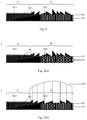
- the optical anti-counterfeiting component 1 comprises: a substrate 101, a sub-wavelength surface micro-structure 1021, an optical reflection facet 1022, and a multi-layer structured coating 103, wherein, the sub-wavelength surface micro-structure 1021 is formed on an upper surface 102 of the substrate 101, and the sub-wavelength surface micro-structure 1021 at least partially cover the upper surface 102; the optical reflection facet 1022 is formed on the upper surface 102 of the substrate 101, and the optical reflection facet 1021 at least partially covers the upper surface 102; a region in which the sub-wavelength surface micro-structure 1021 lies is denoted as region A, and a region in which the optical reflection facet 1022 lies is denoted as region B; the multi-layer structured coating 103 at least partially covers the region A and the region B.
- the region A and the region B are different from each other in color; moreover, the region B has an optical scattering characteristic provided by substantially random change distributed in a two-dimensional plane in which the optical facet lies according to the orientation of the optical facet, and/or the region B can be perceived by the observer as a surface protruding forward and/or backward relative to its actual spatial shape according to the selected orientation of the optical facet.
- the sub-wavelength surface micro-structure can be a one-dimensional grating or two-dimensional grating, and the groove shape of the sub-wavelength surface micro-structure can be sinusoidal, rectangular, or zigzag shape, etc.; the grating distribution of the two-dimensional grating can be in an orthogonal structure, honeycomb structure, two-dimensional Bravais lattice structure, or random structure, etc.
- the structure of the sub-wavelength surface micro-structure is not limited to the above-mentioned structures; moreover, a structure joined or combined from those structures can be used for the sub-wavelength surface micro-structure in the actual optical anti-counterfeiting component.
- patterns such as text and logo, etc. required for anti-counterfeiting can be realized.
- the groove depth of the sub-wavelength surface micro-structure is 10nm-500nm, and more preferably is 50nm-300nm.
- the characteristic dimension of the sub-wavelength surface micro-structure in a two-dimensional plane in which the sub-wavelength surface micro-structure lies is 50nm-500nm, and preferably is 200nm-400nm.
- the characteristic dimension in one direction meets that requirement, the characteristic dimension in other direction is not limited.
- the period and the groove depth of the sub-wavelength surface micro-structure have a certain matching relationship with each other, that matching relationship can be represented by a depth-width ratio (i.e., ratio of groove depth to period), which can be calculated by strict coupled wave theoretical design according to the specific reproduction effect.
- a depth-width ratio i.e., ratio of groove depth to period
- the range of the depth-width ratio generally is 0.3-2, and more preferably is 0.4-1.
- the duty cycle of the sub-wavelength surface micro-structure (i.e., ratio of grating ridge width to period) is also an important parameter that has an influence on the optical effect.
- the duty cycle mainly has an influence on the brightness and contrast of the optical anti-counterfeiting component.
- the duty cycle should be 0.3-0.7, and preferably is 0.4-0.6.
- the multi-layer structured coating 103 can be in a multi-layer dielectric film structure, i.e., consisting of different dielectric layers that have high or low refractivity. Such structure is generally designed with a ⁇ /4 film system.
- the materials of the dielectric layers can be one or more of inorganic coating film materials such as MgF 2 , SiO 2 , Al 2 O 3 , MgO, HfO 2 , TiO 2 , ZnS, and ZnO, etc.
- the dielectric layers can employ high molecular polymers, or employ the combination of inorganic coating film materials and high molecular polymers.
- the structure of the multi-layer structured coating 103 can be a metal/dielectric multi-layer film structure, and generally employs three-layer structure or five-layer structure.
- the structure of the multi-layer structured coating 103 can comprise at least one of the following structures:
- a multi-layer structured coating in a three-layer structure consists of a reflecting layer, a dielectric layer and an absorbing layer, or consists of an absorbing layer, a dielectric layer and an absorbing layer, wherein, the former has an optical variable effect on one side only, while the latter has an optical variable effect on both sides.
- a multi-layer structured coating in a five-layer structure consists of an absorbing layer, a dielectric layer, a reflecting layer, a dielectric layer and an absorbing layer, or consists of an absorbing layer, a dielectric layer, an absorbing layer, a dielectric layer and an absorbing layer.
- the multi-layer structured coating in a five-layer structure has optical variable effects in both sides, and the optical variable effects can be designed as being identical to each other or different from each other, depending on the parameters and materials of the reflecting layer, dielectric layer, and absorbing layer.
- the above-mentioned reflecting layer generally is a metal layer in larger thickness that is generally greater than 20nm, and the material of the reflecting layer can be one or more of Au, Ag, Al, Fe, Sn, Zn, Ni, and Cr, etc.
- the above-mentioned dielectric layers can be single-layer dielectric layers, the dielectric materials of the dielectric layers can be selected from inorganic coating film materials such as MgF 2 , SiO 2 , Al 2 O 3 , MgO, PMMA, HfO 2 , TiO 2 , ZnS, and ZnO or the like and high molecular polymers, and the thickness generally is 10nm-1000nm, and preferably is 50nm-800nm, depending on the optical effect to be achieved and the refractivity of material.
- the dielectric layers can be multi-layer dielectric layers
- the dielectric materials of the dielectric layers can be selected from commonly used inorganic coating film materials such as MgF 2 , SiO 2 , Al 2 O 3 , MgO, PMMA, HfO 2 , TiO 2 , ZnS, and ZnO or the like, and the multi-layered dielectric films are generally used with a ⁇ /4 film system design of high and low refractivity.
- the materials of the absorbing layers can be one or more of metal materials such as Au, Ag, Cu, Al, Fe, Sn, Zn, Ni, and Cr and the like or metallic compounds, the thickness generally doesn't exceed 20nm, and preferably is 5-10nm, for the purpose of partial reflection, partial transmission, and partial absorption of the illumination light.
- the structure of the multi-layer structured coating 103 according to the present invention is not limited to the above-mentioned structure; for example, a two-layer structure (i.e., a reflecting layer and a dielectric layer), a four-layer structure (i.e., an absorbing layer, a dielectric layer, a reflecting layer, and a dielectric layer), etc., are also permitted.
- the multi-layer structured coating 103 can form a Fabry-Perot resonant cavity, which has a selective absorption and reflection effect for incident white light, so that the exiting light only contains specific wave bands, and thereby specific colors are formed; when the incident angle or exit angle of the light changes, the corresponding light path will change, and the interference wave band will change too, resulting in change of the colors presented to the observer, and thereby an optical variable effect in specific colors is created.
- the optical characteristics obtained from a combination of the sub-wavelength surface micro-structure and the multi-layer structured coating the parameter matching relationship, specific principle, and optical characteristics have been defined specifically in the Chinese Patent No. CN102514443 , the content of which is included in the present invention.
- a color change characteristic that the color changes with the viewing angle is created, and is different from a color characteristic solely provided by a multi-layer structured coating with a flat or smooth surface; thus, a unique color change characteristic that the color changes with the viewing angle is created.
- the characteristic dimension or period of the optical reflection facet 1022 in at least one dimension of a two-dimensional plane in which the optical reflection facet 1022 lies is 1 ⁇ m-300 ⁇ m, preferably is 3 ⁇ m-100 ⁇ m, and particularly preferably is 5 ⁇ m-30 ⁇ m.
- the depth of the optical reflection facet is smaller than 10 ⁇ m, and preferably is 1 ⁇ m-5 ⁇ m. Thus, the facet has no light diffraction effect in the visible wavelength range.
- the orientation of the optical reflection facet can be determined according to its inclination angle and/or azimuth angle.
- the characteristics of the multi-layer structured coating 103 on a flat surface include characteristics in two aspects: its color and color change with viewing angle.
- the color characteristic provided by the multi-layer structured coating 103 is not changed in actual by the combination of the optical reflection facet 1022 and the multi-layer structured coating 103, i.e., the multi-layer structured coating has the same selective absorption and reflection characteristics as a multi-layer structured coating formed on a flat surface; for a specific light source, only the direction of emergent light is modified corresponding to each optical reflection facet; hence, in actual, the distribution of the viewing angle of the color change characteristic of the multi-layer structured coating 103 on the two-dimensional surface in the region B is modified.
- the region A and the region B are different from each other in color characteristic and color change characteristic.
- the sub-wavelength surface micro-structure 1021 and the optical reflection facet 1022 can be transferred onto the surface of the substrate 101 by producing a master mask by holographic interferometry, laser photolithography, or electron-beam lithography, producing a work mask through an electroforming process, and then through a mold pressing or UV duplication process, etc.
- the sub-wavelength surface micro-structure and the optical reflection facet have different requirements for the photoresist material of the master mask or the manufacturing process of the master mask. Actually, it is quite difficult to combine them on the same master mask or work mask through the same process. In actual practice, for example, the combination can be accomplished through two steps: First, producing the sub-wavelength surface micro-structure by holographic interferometry; then, producing the optical reflection facet by laser direct writing through a registration photoetching process.
- the multi-layer structured coating 103 generally can be formed through an vacuum coating process, such as thermal evaporation, electron beam evaporation, high-frequency sputtering, magnetron sputtering, ion sputtering, reactive sputtering, or ion coating, etc., or some of the layers can be formed through a chemical plating, electroplating, or spreading process, etc.
- an vacuum coating process such as thermal evaporation, electron beam evaporation, high-frequency sputtering, magnetron sputtering, ion sputtering, reactive sputtering, or ion coating, etc.
- the multi-layer structured coating covering the sub-wavelength surface micro-structure 1021 and the optical reflection facet 1022 is generally formed in the same process, for the sake of simplifying the production process. Therefore, the parameters of the multi-layer structured coating on the surface of the sub-wavelength surface micro-structure 1021 are essentially the same as those of the multi-layer structured coating on the surface of the optical reflection facet 1022.
- the optical reflection facet 1022 has an optical scattering characteristic provided by substantially random change distributed in a two-dimensional plane in which the optical reflection facet 1022 lies, and the region B can be perceived by the observer as a surface that protrudes forward and/or backward relative to its actual spatial shape according to the selected orientation of the optical reflection facet 1022.
- FIG. 2(a) has a random or pseudo-random alignment in a two-dimensional plane where the structure is, and the structural parameters include the depth, width, inclination angle, and azimuth angle of the optical reflection facet; thus, after the incident light is selectively absorbed and reflected by the multi-layer structured coating on the surface of the optical reflection facet, the reflected light has a random or pseudo-random exit direction, and thereby forms an optical scattering characteristic.
- Fig. 2(b) shows that the optical reflection facet 1022 is utilized to simulate a curved surface 1022' and thereby forms a characteristic of protruding from the surface 102 in the region B.
- any optical reflection facet in the two-dimensional plane has substantially similar normal direction as the simulated curved surface 1022' at that position.
- Fig. 3 shows an embodiment in which a region C and associated anti-counterfeiting characteristics are further added on the basis of the optical anti-counterfeiting component 1 according to the present invention, wherein, the sub-wavelength surface micro-structure 1021 and the optical reflection facet 1022 are overlapped to form the region C on the upper surface 102 of the substrate 101.
- the anti-counterfeiting characteristics include the two anti-counterfeiting characteristics mentioned above, i.e., the anti-counterfeiting characteristic obtained by virtue of the combination of the sub-wavelength surface micro-structure 1021 and the multi-layer structured coating 103 and the anti-counterfeiting characteristic obtained by virtue of the combination of the optical reflection facet 1022 and the multi-layer structured coating 103.
- the anti-counterfeiting characteristics of the region C have the color and color change characteristics formed by the sub-wavelength surface micro-structure 1021 and the multi-layer structured coating 103 different from those of the multi-layer structured coating, as well as the optical scattering characteristic resulted from random distribution of the optical reflection facets 1022 on the two-dimensional surface of the region C and/or the characteristic of a surface protruding forward and/or backward relative to the surface of the region C as perceived by the observer.
- the sub-wavelength surface micro-structure 1021 has sinusoidal groove shape, 300nm period, and 95nm depth, and is in orthogonal two-dimensional grid distribution
- the multi-layer structured coating 103 includes sequentially arranged Al (40nm)/SiO 2 (370nm)/Cr (5nm) layers (on a flat surface
- the multi-layer structured coating that has the above-mentioned parameter has a characteristic that it exhibits a golden yellow color when it is viewed from the front side and exhibits a green color when it is viewed obliquely).
- the region A exhibits a red color when it is viewed from the front side, and exhibits a yellow color when it is viewed inclined;
- the region B has the characteristic of color change from golden yellow to green provided by the multi-layer structured coating and the optical scattering characteristic and/or protruding characteristic provided by the optical reflection facet;
- the region C has the characteristic of color change from red to yellow formed by the sub-wavelength surface micro-structure and the multi-layer structured coating jointly and the optical scattering characteristic and/or protruding characteristic provided by the optical reflection facet.
- the three regions A, B and C have their respective visual characteristics and form a strong visual contrast to each other; thus, the optical anti-counterfeiting component 1 has strong anti-counterfeiting capability.
- the coverage of the multi-layer structured coating is patterned, and thereby forms an hollowed-out feature.
- the entire multi-layer structured coating can be patterned, or one or more layers of the multi-layer structured coating can be patterned respectively.
- a patterned protective layer is applied after the multi-layer structured coating is formed by printing, and then the coating outside of the protective area is etched with a chemical solvent (e.g., alkaline liquor).
- a stripping layer is formed before the multi-layer structured coating is formed, and the coating on the stripping layer is removed by soaking with a liquid (e.g., water) to form a hollowed-out pattern after the multi-layer structured coating is formed.
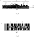
- the hollowed-out pattern 1031 of the multi-layer structured coating 103 (uncovered region of the multi-layer structured coating) has a strict position correspondence relationship with the sub-wavelength surface micro-structure 1021 and/or optical reflection facet 1022; thus, the optical anti-counterfeiting component according to the present invention can be identified more easily and has stronger forgery prevention capability.
- A, B, C correspond to the three regions A, B and C in Fig.
- CBPM and ZSST have a color characteristic and a characteristic of color change with viewing angle, which are formed by the sub-wavelength surface micro-structure and the multi-layer structured coating formed on the surface of the sub-wavelength surface micro-structure jointly and are different from those in the region B and region C;
- the region B has an optical scattering characteristic and a characteristic of color change with viewing angle, which are formed by the optical reflection facet and the multi-layer structured coating formed on the surface of the optical reflection facet jointly;
- region C has a characteristic of surface protruding forward relative to the actual spatial shape and a characteristic of color change with viewing angle, which are resulted from the optical reflection facet and the multi-layer structured coating formed on the surface of the optical reflection facet.
- a sinusoidal optical grating is formed in the region 1031, the period of the sinusoidal optical grating is 350nm, and the deep of the sinusoidal optical grating is 300nm (suppose the depth-width ratio of that structure is greater than that of the surface micro-structure outside of the region 1031).
- an Al layer in 5nm thickness and a SiO 2 layer in 250nm thickness are deposited on the top surface 102; next, the optical anti-counterfeiting component 1 is soaked in 10% NaOH solution, till that the Al layer in the region 1031 completely disappears rightly; at this point, the surface outside of the region 1031 is still covered by the Al layer and SiO 2 layer. Then, an Al layer in 40nm thickness is deposited on the SiO 2 layer, and a SiO 2 layer in 50nm thickness is deposited on the surface of the new Al layer; next, the optical anti-counterfeiting component 1 is soaked in 5% NaOH solution, till the Al layer in the region 1031 completely disappears rightly.
- cylindrical mirrors are formed in the region 1031, the width of the cylindrical mirror is 30 ⁇ m, the clearance between the cylindrical mirrors is 2 ⁇ m, and the height of the cylindrical mirror is 10 ⁇ m (greater than the 1.5 ⁇ m height of the optical reflection facet); an Al layer in 40nm thickness (thickness in the flat area), a SiO 2 layer in 250nm thickness, and a Cr layer in 5nm thickness are deposited sequentially on the surface 102, and then a protective layer (polyester material) in 1 ⁇ m thickness (thickness of the flat surface) is formed through a spreading process.
- a protective layer polyyester material
- the optical anti-counterfeiting component is soaked in 10% NaOH solution at 40°C, till the Al/SiO 2 /Cr coating in the region 1031 just completely disappears; at this point, the area outside of the region 1031 is stilled covered by the Al/SiO 2 /Cr coating; thus, the optical anti-counterfeiting component is prepared.
- a multi-layer structured coating is provided by the sequentially stacked Al/SiO 2 /Cr layers in the area outside of the region 1031, and a hollowed-out pattern is formed in the region 1031.
- one or more of diffraction optical variable feature, micro-nano structural feature, printing feature, fluorescent feature, and magnetic, optical, electrical, or radioactive feature for machine reading can be formed in the substrate 101 and on the upper and lower surfaces of the substrate 101, and/or in and on the sub-wavelength surface micro-structure and optical reflection facet.
- the optical anti-counterfeiting component according to the present invention can be used as a tag, logo, wide strip, transparent window, or overlaying film, etc., and can be bonded to different articles by means of different bonding mechanisms. For example, it can be transferred onto high-security products and high added-value products, such as bank notes and credit cards, etc.
- the present invention provides a product with the optical anti-counterfeiting component, which includes, but is not limited to various high-security products and high added-value products such as bank notes, credit cards, passports, valuable securities, etc., and various packing paper and packing boxes, etc.
Landscapes
- Engineering & Computer Science (AREA)
- Physics & Mathematics (AREA)
- General Physics & Mathematics (AREA)
- Theoretical Computer Science (AREA)
- Manufacturing & Machinery (AREA)
- Business, Economics & Management (AREA)
- Accounting & Taxation (AREA)
- Finance (AREA)
- Credit Cards Or The Like (AREA)
- Diffracting Gratings Or Hologram Optical Elements (AREA)
Description
- The present invention relates to the optical anti-counterfeiting field, in particular to an optical anti-counterfeiting component and an optical anti-counterfeiting product.
- To prevent forgery of various high-security or high added-value prints, such as banknotes, certificates, and product packages, etc., a multi-layer structured coating technique is widely applied. The multi-layer structured coating technique can present different color characteristics or present different colors at different viewing angles, which can't be imitated or duplicated by means of electronic devices such as cameras, scanners, and printers, etc.; therefore, it has high anti-counterfeiting capability. However, the requirements in the anti-counterfeiting field can't be satisfied well by multi-layer coating technique solely nowadays.
- In the prior art, optical variable magnetic ink (OVMI) is formed by adding a magnetic layer in an optical variable structure, and the OVMI particles can be induced by the magnetic field to align directionally in the directions of the magnetic induction lines, so that specific graphic and text structures can be formed. However, owing to the fact that the optical variable magnetic particles rely on a magnetic field to achieve a directional alignment, the shape can't be designed freely under the constraints of the shape of the magnetic field; in addition, special orientation equipment and process are required to achieve directional alignment of the optical variable magnetic particles. Moreover, a technical integration solution that combines interferential multi-layer coating with holographic technique, and color matching technique, etc. is complex, and the corresponding effect is not ideal. Therefore, with such a technical integration solution, the improvement of anti-counterfeiting capability of the interferential multi-layer coating is still limited.
-
WO 2014/0192269 -
CN103847 289 discloses an anti-counterfeiting element having a base material with at least part of the surface provided with one or various blazing micro structures. The azimuthal angle and blazing angles of the blazing micro structures are arranged according to a certain mode so that when the blazing micro structures are illuminated, hidden images can be asymmetrically represented at the position which is a certain distance away from the optical anti-counterfeiting element. Thus an optical anti-counterfeiting element which has a hidden image representation function can be provided. - The object of the present invention is to provide an optical anti-counterfeiting component and an optical anti-counterfeiting product, in order to improve performance of the anti-counterfeiting products.
- The present invention provides an optical anti-counterfeiting component as defined in
claim 1. - Preferably, the sub-wavelength surface micro-structure and the optical reflection facet overlap with each other partially.
- Preferably, the multi-layer structured coating forms a Fabry-Perot resonant cavity.
- Preferably, the multi-layer structured coating forms a hollowed-out pattern.
- Preferably, the hollowed-out pattern has a registration relationship with the sub-wavelength surface micro-structure and/or the optical reflection facet.
- Preferably, the sub-wavelength surface micro-structure is an one-dimensional grating or a two-dimensional grating; a groove shape of the sub-wavelength surface micro-structure is sinusoidal, rectangular, or zigzag shape, or a shape joined or combined from at least two of sinusoidal, rectangular, and zigzag shapes.
- Preferably, a groove depth of the sub-wavelength surface micro-structure is 10nm-500nm.
- Preferably, the groove depth of the sub-wavelength surface micro-structure is 50nm-300nm.
- Preferably, a characteristic dimension of the sub-wavelength surface micro-structure in a two-dimensional plane in which the sub-wavelength surface micro-structure lies is 50nm-500nm.
- Preferably, the characteristic dimension of the sub-wavelength surface micro-structure in a two-dimensional plane in which the sub-wavelength surface micro-structure lies is 200nm-400nm.
- Preferably, a characteristic dimension of the optical reflection facet in at least one dimension of a two-dimensional plane in which the optical reflection facet lies is 1µm-300µm.
- Preferably, the characteristic dimension of the optical reflection facet in at least one dimension of a two-dimensional plane in which the optical reflection facet lies is 3µm-100µm.
- Preferably, the characteristic dimension of the optical reflection facet in at least one dimension in a two-dimensional plane in which the optical reflection facet lies is 5µm-30µm.
- Preferably, at least one of diffraction optical variable feature, micro-nano structural feature, printing feature, fluorescent feature, and magnetic, optical, electrical, or radioactive feature for machine reading is formed on at least one of the substrate, the sub-wavelength surface micro-structure, and the optical reflection facet.
- Preferably, the multi-layer structured coating consists of an absorbing layer, a dielectric layer, and a reflecting layer.
- The present invention further provides an optical anti-counterfeiting product, which includes the optical anti-counterfeiting component.
- In the case where the same multi-layer structured coating is used, a contrasting optical characteristic is formed between the region in which the sub-wavelength surface micro-structure and the multi-layer structured coating lie and the region in which the optical reflection facet and the multi-layer structured coating lie, so that the optical anti-counterfeiting component or the optical anti-counterfeiting product that includes the optical anti-counterfeiting component can be identified easily and has high anti-counterfeiting capability.
- Other features and advantages of the present invention will be further detailed in the embodiments hereunder.
- The accompanying drawings are provided here to facilitate further understanding on the present invention, and constitute a part of this document. They are used in conjunction with the following embodiments to explain the present invention, but shall not be comprehended as constituting any limitation to the present invention. Among the drawings:
-
Fig. 1 is a sectional view of the optical anti-counterfeiting component according to an embodiment of the present invention; -
Fig. 2(a) and 2(b) are sectional views of the optical anti-counterfeiting component according to another embodiment of the present invention; -
Fig. 3 is a sectional view of the optical anti-counterfeiting component according to yet another embodiment of the present invention; -
Fig. 4 is a top view of the optical anti-counterfeiting component according to yet another embodiment of the present invention. - Hereunder some embodiments of the present invention will be detailed with reference to the accompanying drawings. It should be appreciated that the embodiments described here are only provided to describe and explain the present invention, but shall not be deemed as constituting any limitation to the present invention.
- The present invention provides an optical
anti-counterfeiting component 1. As shown inFig. 1 , the optical anti-counterfeiting component 1 comprises: a substrate 101, a sub-wavelength surface micro-structure 1021, an optical reflection facet 1022, and a multi-layer structured coating 103, wherein, the sub-wavelength surface micro-structure 1021 is formed on an upper surface 102 of the substrate 101, and the sub-wavelength surface micro-structure 1021 at least partially cover the upper surface 102; the optical reflection facet 1022 is formed on the upper surface 102 of the substrate 101, and the optical reflection facet 1021 at least partially covers the upper surface 102; a region in which the sub-wavelength surface micro-structure 1021 lies is denoted as region A, and a region in which the optical reflection facet 1022 lies is denoted as region B; the multi-layer structured coating 103 at least partially covers the region A and the region B. Since the multi-layer structured coating 103 covers the region A and the region B, the region A and the region B are different from each other in color; moreover, the region B has an optical scattering characteristic provided by substantially random change distributed in a two-dimensional plane in which the optical facet lies according to the orientation of the optical facet, and/or the region B can be perceived by the observer as a surface protruding forward and/or backward relative to its actual spatial shape according to the selected orientation of the optical facet. - The sub-wavelength surface micro-structure can be a one-dimensional grating or two-dimensional grating, and the groove shape of the sub-wavelength surface micro-structure can be sinusoidal, rectangular, or zigzag shape, etc.; the grating distribution of the two-dimensional grating can be in an orthogonal structure, honeycomb structure, two-dimensional Bravais lattice structure, or random structure, etc. It should be understood that the structure of the sub-wavelength surface micro-structure is not limited to the above-mentioned structures; moreover, a structure joined or combined from those structures can be used for the sub-wavelength surface micro-structure in the actual optical anti-counterfeiting component. By designing the sub-wavelength surface micro-structure, patterns such as text and logo, etc. required for anti-counterfeiting can be realized.
- Preferably, the groove depth of the sub-wavelength surface micro-structure is 10nm-500nm, and more preferably is 50nm-300nm. In addition, the characteristic dimension of the sub-wavelength surface micro-structure in a two-dimensional plane in which the sub-wavelength surface micro-structure lies is 50nm-500nm, and preferably is 200nm-400nm. Preferably, if the characteristic dimension in one direction meets that requirement, the characteristic dimension in other direction is not limited.
- Preferably, the period and the groove depth of the sub-wavelength surface micro-structure have a certain matching relationship with each other, that matching relationship can be represented by a depth-width ratio (i.e., ratio of groove depth to period), which can be calculated by strict coupled wave theoretical design according to the specific reproduction effect. Preferably, the range of the depth-width ratio generally is 0.3-2, and more preferably is 0.4-1.
- Preferably, the duty cycle of the sub-wavelength surface micro-structure (i.e., ratio of grating ridge width to period) is also an important parameter that has an influence on the optical effect. The duty cycle mainly has an influence on the brightness and contrast of the optical anti-counterfeiting component. Generally, the duty cycle should be 0.3-0.7, and preferably is 0.4-0.6.
- Hereunder the structure of the multi-layer structured
coating 103 employed in the opticalanti-counterfeiting component 1 according to the present invention will be described. - The multi-layer structured
coating 103 can be in a multi-layer dielectric film structure, i.e., consisting of different dielectric layers that have high or low refractivity. Such structure is generally designed with a λ/4 film system. The materials of the dielectric layers can be one or more of inorganic coating film materials such as MgF2, SiO2, Al2O3, MgO, HfO2, TiO2, ZnS, and ZnO, etc. Alternatively, the dielectric layers can employ high molecular polymers, or employ the combination of inorganic coating film materials and high molecular polymers. - Alternatively, the structure of the multi-layer
structured coating 103 can be a metal/dielectric multi-layer film structure, and generally employs three-layer structure or five-layer structure. For example, the structure of the multi-layerstructured coating 103 can comprise at least one of the following structures: - a. a reflecting layer, a dielectric layer and an absorbing layer formed orderly on the sub-wavelength surface micro-structure, or formed in a reversed order;
- b. an absorbing layer, a dielectric layer and an absorbing layer formed orderly on the sub-wavelength surface micro-structure, or formed in a reversed order;
- c. an absorbing layer, a dielectric layer, a reflecting layer, a dielectric layer, and an absorbing layer formed orderly on the sub-wavelength surface micro-structure;
- d. an absorbing layer, a dielectric layer, an absorbing layer, a dielectric layer, and an absorbing layer formed orderly on the sub-wavelength surface micro-structure.
- In brief, a multi-layer structured coating in a three-layer structure consists of a reflecting layer, a dielectric layer and an absorbing layer, or consists of an absorbing layer, a dielectric layer and an absorbing layer, wherein, the former has an optical variable effect on one side only, while the latter has an optical variable effect on both sides. A multi-layer structured coating in a five-layer structure consists of an absorbing layer, a dielectric layer, a reflecting layer, a dielectric layer and an absorbing layer, or consists of an absorbing layer, a dielectric layer, an absorbing layer, a dielectric layer and an absorbing layer. The multi-layer structured coating in a five-layer structure has optical variable effects in both sides, and the optical variable effects can be designed as being identical to each other or different from each other, depending on the parameters and materials of the reflecting layer, dielectric layer, and absorbing layer.
- The above-mentioned reflecting layer generally is a metal layer in larger thickness that is generally greater than 20nm, and the material of the reflecting layer can be one or more of Au, Ag, Al, Fe, Sn, Zn, Ni, and Cr, etc. The above-mentioned dielectric layers can be single-layer dielectric layers, the dielectric materials of the dielectric layers can be selected from inorganic coating film materials such as MgF2, SiO2, Al2O3, MgO, PMMA, HfO2, TiO2, ZnS, and ZnO or the like and high molecular polymers, and the thickness generally is 10nm-1000nm, and preferably is 50nm-800nm, depending on the optical effect to be achieved and the refractivity of material. Of course, the dielectric layers can be multi-layer dielectric layers, the dielectric materials of the dielectric layers can be selected from commonly used inorganic coating film materials such as MgF2, SiO2, Al2O3, MgO, PMMA, HfO2, TiO2, ZnS, and ZnO or the like, and the multi-layered dielectric films are generally used with a λ/4 film system design of high and low refractivity. The materials of the absorbing layers can be one or more of metal materials such as Au, Ag, Cu, Al, Fe, Sn, Zn, Ni, and Cr and the like or metallic compounds, the thickness generally doesn't exceed 20nm, and preferably is 5-10nm, for the purpose of partial reflection, partial transmission, and partial absorption of the illumination light.
- It should be understood that the structure of the multi-layer
structured coating 103 according to the present invention is not limited to the above-mentioned structure; for example, a two-layer structure (i.e., a reflecting layer and a dielectric layer), a four-layer structure (i.e., an absorbing layer, a dielectric layer, a reflecting layer, and a dielectric layer), etc., are also permitted. - The multi-layer
structured coating 103 can form a Fabry-Perot resonant cavity, which has a selective absorption and reflection effect for incident white light, so that the exiting light only contains specific wave bands, and thereby specific colors are formed; when the incident angle or exit angle of the light changes, the corresponding light path will change, and the interference wave band will change too, resulting in change of the colors presented to the observer, and thereby an optical variable effect in specific colors is created.
As for the optical characteristics obtained from a combination of the sub-wavelength surface micro-structure and the multi-layer structured coating, the parameter matching relationship, specific principle, and optical characteristics have been defined specifically in the Chinese Patent No.CN102514443 , the content of which is included in the present invention. In summary, by virtue of a combination of thesub-wavelength surface micro-structure 1021 and the multi-layerstructured coating 103, a color change characteristic that the color changes with the viewing angle is created, and is different from a color characteristic solely provided by a multi-layer structured coating with a flat or smooth surface; thus, a unique color change characteristic that the color changes with the viewing angle is created. - Hereunder the optical characteristics provided by virtue of a combination of the
optical reflection facet 1022 and the multi-layerstructured coating 103 will be described with reference toFig. 1 . - The characteristic dimension or period of the
optical reflection facet 1022 in at least one dimension of a two-dimensional plane in which theoptical reflection facet 1022 lies (the facet can be formed to be periodic or aperiodic) is 1µm-300µm, preferably is 3µm-100µm, and particularly preferably is 5µm-30µm. The depth of the optical reflection facet is smaller than 10µm, and preferably is 1µm-5µm. Thus, the facet has no light diffraction effect in the visible wavelength range. - The orientation of the optical reflection facet can be determined according to its inclination angle and/or azimuth angle.
- As for the optical characteristics obtained from a combination of the
optical reflection facet 1022 and the multi-layerstructured coating 103, the specific parameter setting, principle, and optical characteristics have been defined by Chinese Patent No.CN102514443 ,CN102905909 ,CN103282212 andCN103229078 jointly. - The characteristics of the multi-layer
structured coating 103 on a flat surface include characteristics in two aspects: its color and color change with viewing angle. The color characteristic provided by the multi-layerstructured coating 103 is not changed in actual by the combination of theoptical reflection facet 1022 and the multi-layerstructured coating 103, i.e., the multi-layer structured coating has the same selective absorption and reflection characteristics as a multi-layer structured coating formed on a flat surface; for a specific light source, only the direction of emergent light is modified corresponding to each optical reflection facet; hence, in actual, the distribution of the viewing angle of the color change characteristic of the multi-layerstructured coating 103 on the two-dimensional surface in the region B is modified. - Owing to the above-mentioned result, in a case where the same multi-layer
structured coating 103 is used, the region A and the region B are different from each other in color characteristic and color change characteristic. - The
sub-wavelength surface micro-structure 1021 and theoptical reflection facet 1022 can be transferred onto the surface of thesubstrate 101 by producing a master mask by holographic interferometry, laser photolithography, or electron-beam lithography, producing a work mask through an electroforming process, and then through a mold pressing or UV duplication process, etc. - Since the dimension parameters of the sub-wavelength surface micro-structure are greatly different by orders of magnitude from those of the optical reflection facet, the sub-wavelength surface micro-structure and the optical reflection facet have different requirements for the photoresist material of the master mask or the manufacturing process of the master mask. Actually, it is quite difficult to combine them on the same master mask or work mask through the same process. In actual practice, for example, the combination can be accomplished through two steps: First, producing the sub-wavelength surface micro-structure by holographic interferometry; then, producing the optical reflection facet by laser direct writing through a registration photoetching process.
- The multi-layer
structured coating 103 generally can be formed through an vacuum coating process, such as thermal evaporation, electron beam evaporation, high-frequency sputtering, magnetron sputtering, ion sputtering, reactive sputtering, or ion coating, etc., or some of the layers can be formed through a chemical plating, electroplating, or spreading process, etc. - It should be noted that the multi-layer structured coating covering the
sub-wavelength surface micro-structure 1021 and theoptical reflection facet 1022 is generally formed in the same process, for the sake of simplifying the production process. Therefore, the parameters of the multi-layer structured coating on the surface of thesub-wavelength surface micro-structure 1021 are essentially the same as those of the multi-layer structured coating on the surface of theoptical reflection facet 1022. Hence, an overall consideration should be made in the structural design of the film system of the multi-layerstructured coating 103 and the structural design calculation of thesub-wavelength surface micro-structure 1021 andoptical reflection facet 1022, so that the optical characteristics in the region A have a strong color contrast to the optical characteristics in the region B, and thereby the purpose of easy identification and forgery prevention for the anti-counterfeiting component is achieved. - Hereunder the optical characteristics of the optical anti-counterfeiting component will be described with reference to
Figs. 2(a) and 2(b) respectively. In the opticalanti-counterfeiting component 1 according to the present invention, theoptical reflection facet 1022 has an optical scattering characteristic provided by substantially random change distributed in a two-dimensional plane in which theoptical reflection facet 1022 lies, and the region B can be perceived by the observer as a surface that protrudes forward and/or backward relative to its actual spatial shape according to the selected orientation of theoptical reflection facet 1022. The structure of theoptical reflection facet 1022 that has different parameters in the region B inFig. 2(a) has a random or pseudo-random alignment in a two-dimensional plane where the structure is, and the structural parameters include the depth, width, inclination angle, and azimuth angle of the optical reflection facet; thus, after the incident light is selectively absorbed and reflected by the multi-layer structured coating on the surface of the optical reflection facet, the reflected light has a random or pseudo-random exit direction, and thereby forms an optical scattering characteristic.Fig. 2(b) shows that theoptical reflection facet 1022 is utilized to simulate a curved surface 1022' and thereby forms a characteristic of protruding from thesurface 102 in the region B. Here, any optical reflection facet in the two-dimensional plane has substantially similar normal direction as the simulated curved surface 1022' at that position. -
Fig. 3 shows an embodiment in which a region C and associated anti-counterfeiting characteristics are further added on the basis of the opticalanti-counterfeiting component 1 according to the present invention, wherein, thesub-wavelength surface micro-structure 1021 and theoptical reflection facet 1022 are overlapped to form the region C on theupper surface 102 of thesubstrate 101. The anti-counterfeiting characteristics include the two anti-counterfeiting characteristics mentioned above, i.e., the anti-counterfeiting characteristic obtained by virtue of the combination of thesub-wavelength surface micro-structure 1021 and the multi-layerstructured coating 103 and the anti-counterfeiting characteristic obtained by virtue of the combination of theoptical reflection facet 1022 and the multi-layerstructured coating 103. That is to say, the anti-counterfeiting characteristics of the region C have the color and color change characteristics formed by thesub-wavelength surface micro-structure 1021 and the multi-layerstructured coating 103 different from those of the multi-layer structured coating, as well as the optical scattering characteristic resulted from random distribution of theoptical reflection facets 1022 on the two-dimensional surface of the region C and/or the characteristic of a surface protruding forward and/or backward relative to the surface of the region C as perceived by the observer. - For example, in
Fig. 3 , thesub-wavelength surface micro-structure 1021 has sinusoidal groove shape, 300nm period, and 95nm depth, and is in orthogonal two-dimensional grid distribution, and the multi-layerstructured coating 103 includes sequentially arranged Al (40nm)/SiO2 (370nm)/Cr (5nm) layers (on a flat surface, the multi-layer structured coating that has the above-mentioned parameter has a characteristic that it exhibits a golden yellow color when it is viewed from the front side and exhibits a green color when it is viewed obliquely). Thus, owing to the existence of thesub-wavelength surface micro-structure 1021, the region A exhibits a red color when it is viewed from the front side, and exhibits a yellow color when it is viewed inclined; the region B has the characteristic of color change from golden yellow to green provided by the multi-layer structured coating and the optical scattering characteristic and/or protruding characteristic provided by the optical reflection facet; the region C has the characteristic of color change from red to yellow formed by the sub-wavelength surface micro-structure and the multi-layer structured coating jointly and the optical scattering characteristic and/or protruding characteristic provided by the optical reflection facet. In summary, the three regions A, B and C have their respective visual characteristics and form a strong visual contrast to each other; thus, the opticalanti-counterfeiting component 1 has strong anti-counterfeiting capability. - Preferably, in the optical anti-counterfeiting component according to the present invention, the coverage of the multi-layer structured coating is patterned, and thereby forms an hollowed-out feature. The entire multi-layer structured coating can be patterned, or one or more layers of the multi-layer structured coating can be patterned respectively. For example, a patterned protective layer is applied after the multi-layer structured coating is formed by printing, and then the coating outside of the protective area is etched with a chemical solvent (e.g., alkaline liquor). Alternatively, a stripping layer is formed before the multi-layer structured coating is formed, and the coating on the stripping layer is removed by soaking with a liquid (e.g., water) to form a hollowed-out pattern after the multi-layer structured coating is formed.
- Preferably, as shown in
Fig. 4 , i.e., a top view of an embodiment of the optical anti-counterfeiting component according to the present invention, the hollowed-out pattern 1031 of the multi-layer structured coating 103 (uncovered region of the multi-layer structured coating) has a strict position correspondence relationship with thesub-wavelength surface micro-structure 1021 and/oroptical reflection facet 1022; thus, the optical anti-counterfeiting component according to the present invention can be identified more easily and has stronger forgery prevention capability. Wherein, A, B, C correspond to the three regions A, B and C inFig. 3 , i.e., "CBPM" and "ZSST" have a color characteristic and a characteristic of color change with viewing angle, which are formed by the sub-wavelength surface micro-structure and the multi-layer structured coating formed on the surface of the sub-wavelength surface micro-structure jointly and are different from those in the region B and region C; the region B has an optical scattering characteristic and a characteristic of color change with viewing angle, which are formed by the optical reflection facet and the multi-layer structured coating formed on the surface of the optical reflection facet jointly; region C has a characteristic of surface protruding forward relative to the actual spatial shape and a characteristic of color change with viewing angle, which are resulted from the optical reflection facet and the multi-layer structured coating formed on the surface of the optical reflection facet. - Hereunder an exemplary method for forming the hollowed-
out region 1031 is provided: a sinusoidal optical grating is formed in theregion 1031, the period of the sinusoidal optical grating is 350nm, and the deep of the sinusoidal optical grating is 300nm (suppose the depth-width ratio of that structure is greater than that of the surface micro-structure outside of the region 1031). Then, an Al layer in 5nm thickness and a SiO2 layer in 250nm thickness are deposited on thetop surface 102; next, the opticalanti-counterfeiting component 1 is soaked in 10% NaOH solution, till that the Al layer in theregion 1031 completely disappears rightly; at this point, the surface outside of theregion 1031 is still covered by the Al layer and SiO2 layer. Then, an Al layer in 40nm thickness is deposited on the SiO2 layer, and a SiO2 layer in 50nm thickness is deposited on the surface of the new Al layer; next, the opticalanti-counterfeiting component 1 is soaked in 5% NaOH solution, till the Al layer in theregion 1031 completely disappears rightly. At this point, when the opticalanti-counterfeiting component 1 is viewed from the side of the lower surface of theregion 1031, it is seen that a multi-layer structured coating is provided in the area outside of theregion 1031. In addition, a hollowed-out pattern is formed in theregion 1031, because there is no coating in the region. - Hereunder another exemplary method for forming the hollowed-
out region 1031 is provided: cylindrical mirrors are formed in theregion 1031, the width of the cylindrical mirror is 30µm, the clearance between the cylindrical mirrors is 2µm, and the height of the cylindrical mirror is 10µm (greater than the 1.5µm height of the optical reflection facet); an Al layer in 40nm thickness (thickness in the flat area), a SiO2 layer in 250nm thickness, and a Cr layer in 5nm thickness are deposited sequentially on thesurface 102, and then a protective layer (polyester material) in 1µm thickness (thickness of the flat surface) is formed through a spreading process. The optical anti-counterfeiting component is soaked in 10% NaOH solution at 40°C, till the Al/SiO2/Cr coating in theregion 1031 just completely disappears; at this point, the area outside of theregion 1031 is stilled covered by the Al/SiO2/Cr coating; thus, the optical anti-counterfeiting component is prepared. At this point, when the optical anti-counterfeiting component is viewed from the side of thetop surface 102, it is seen that a multi-layer structured coating is provided by the sequentially stacked Al/SiO2/Cr layers in the area outside of theregion 1031, and a hollowed-out pattern is formed in theregion 1031. - In preferred embodiments according to the present invention, one or more of diffraction optical variable feature, micro-nano structural feature, printing feature, fluorescent feature, and magnetic, optical, electrical, or radioactive feature for machine reading can be formed in the
substrate 101 and on the upper and lower surfaces of thesubstrate 101, and/or in and on the sub-wavelength surface micro-structure and optical reflection facet. - The optical anti-counterfeiting component according to the present invention can be used as a tag, logo, wide strip, transparent window, or overlaying film, etc., and can be bonded to different articles by means of different bonding mechanisms. For example, it can be transferred onto high-security products and high added-value products, such as bank notes and credit cards, etc.
- In another aspect, the present invention provides a product with the optical anti-counterfeiting component, which includes, but is not limited to various high-security products and high added-value products such as bank notes, credit cards, passports, valuable securities, etc., and various packing paper and packing boxes, etc.
- While some preferred embodiments of the present invention are described above with reference to the accompanying drawings, the present invention is not limited to the details in those embodiments. The invention is limited by the scope of the claims.
- In addition, it should be understood that the technical features described in the above embodiments can be combined in any appropriate manner, provided that there is no conflict among the technical features in the combination. To avoid unnecessary iteration, such possible combinations are not described here in the present invention.
| 101 | | 102 | |
| 103 | Multi-layer | 1021 | Sub-wavelength surface micro-structure |
| 1022 | Optical reflection facet | 1022' | |
Claims (15)
- An optical anti-counterfeiting component (1) comprising:-a substrate (101);a sub-wavelength surface micro-structure (1021) and an optical reflection facet (1022), both of which are formed on the upper surface (102) of said substrate (101);wherein at least part of the upper surface of the substrate (101) is covered by the sub-wavelength surface micro-structure (1021) and the optical reflection facet (1022); anda multi-layer structured coating (103) formed on the sub-wavelength surface micro-structure (1021) and the optical reflection facet (1022), wherein the multi-layer structured coating (103) covering the sub-wavelength surface micro-structure (1021) and the multi-layer structured coating (103) covering the optical reflection facet (1022) are the same multi-layer structured coating (103) which is formed in the same process.
- An optical anti-counterfeiting component according to claim 1, wherein, the sub-wavelength surface micro-structure (1021) and the optical reflection facet (1022) overlap with each other partially.
- An optical anti-counterfeiting component according to claim 1, wherein, the multi-layer structured coating (103) forms a Fabry-Perot resonant cavity.
- An optical anti-counterfeiting component according to claim 1, wherein, the multi-layer structured coating (103) forms a hollowed-out pattern.
- An optical anti-counterfeiting component according to claim 4, wherein the hollowed-out pattern has a registration relationship with the sub-wavelength surface micro-structure (1021) and/or the optical reflection facet (1022).
- An optical anti-counterfeiting component according to claim 1, wherein the sub-wavelength surface micro-structure (1021) is a one-dimensional grating or a two-dimensional grating; a groove shape of the sub-wavelength surface micro-structure (1021) is sinusoidal, rectangular, or zigzag shape, or a shape joined or combined from at least two of sinusoidal, rectangular, and zigzag shapes.
- An optical anti-counterfeiting component according to claim 6, wherein a groove depth of the sub-wavelength surface micro-structure (1021) is 10nm-500nm.
- An optical anti-counterfeiting component according to claim 7, wherein the groove depth of the sub-wavelength surface micro-structure (1021) is 50nm-300nm.
- An optical anti-counterfeiting component according to claim 1, wherein a characteristic dimension of the sub-wavelength surface micro-structure (1021) in a two-dimensional plane in which the sub-wavelength surface micro-structure (1021) lies is 50nm-500nm.
- An optical anti-counterfeiting component according to claim 9, wherein the characteristic dimension of the sub-wavelength surface micro-structure (1021) in a two-dimensional plane in which the sub-wavelength surface micro-structure (1021) lies is 200nm-400nm.
- An optical anti-counterfeiting component according to claim 1, wherein a characteristic dimension of the optical reflection facet (1022) in at least one dimension of a two-dimensional plane in which the optical reflection facet lies is 1µm-300µm.
- An optical anti-counterfeiting component according to claim 11, wherein the characteristic dimension of the optical reflection facet in at least one dimension of a two-dimensional plane in which the optical reflection facet lies is 3µm-100µm.
- An optical anti-counterfeiting component according to claim 1, wherein at least one of a diffraction optical variable feature, micro-nano structural feature, printing feature, fluorescent feature, and magnetic, optical, electrical, or radioactive feature for machine reading is formed on at least one of the substrate (101), the sub-wavelength surface micro-structure (1021), and the optical reflection facet (1022).
- An optical anti-counterfeiting component according to any one of claims 1-13, wherein the multi-layer structured coating (103) consists of at least two of an absorbing layer, a dielectric layer, and a reflecting layer, or the multi-layer structured coating (103) consists of dielectric layers.
- An optical anti-counterfeiting product comprising the optical anti-counterfeiting component of any one of claims 1-14.
Applications Claiming Priority (2)
| Application Number | Priority Date | Filing Date | Title |
|---|---|---|---|
| CN201410548750.2A CN104385800B (en) | 2014-10-16 | 2014-10-16 | Optical anti-counterfeit element and optical anti-counterfeiting product |
| PCT/CN2015/089408 WO2016058465A1 (en) | 2014-10-16 | 2015-09-11 | Optical anti-counterfeiting element and optical anti-counterfeiting product |
Publications (3)
| Publication Number | Publication Date |
|---|---|
| EP3208099A1 EP3208099A1 (en) | 2017-08-23 |
| EP3208099A4 EP3208099A4 (en) | 2018-04-18 |
| EP3208099B1 true EP3208099B1 (en) | 2020-02-19 |
Family
ID=52603795
Family Applications (1)
| Application Number | Title | Priority Date | Filing Date |
|---|---|---|---|
| EP15850046.2A Revoked EP3208099B1 (en) | 2014-10-16 | 2015-09-11 | Optical anti-counterfeiting element and optical anti-counterfeiting product |
Country Status (5)
| Country | Link |
|---|---|
| US (1) | US10421308B2 (en) |
| EP (1) | EP3208099B1 (en) |
| CN (1) | CN104385800B (en) |
| RU (1) | RU2670078C1 (en) |
| WO (1) | WO2016058465A1 (en) |
Cited By (1)
| Publication number | Priority date | Publication date | Assignee | Title |
|---|---|---|---|---|
| EP4121299B1 (en) | 2020-03-16 | 2023-07-26 | Hueck Folien Gesellschaft m.b.H. | Flat security element with optical security features |
Families Citing this family (23)
| Publication number | Priority date | Publication date | Assignee | Title |
|---|---|---|---|---|
| CN104385800B (en) | 2014-10-16 | 2017-10-24 | 中钞特种防伪科技有限公司 | Optical anti-counterfeit element and optical anti-counterfeiting product |
| CN104875523B (en) * | 2015-05-22 | 2016-06-29 | 中钞特种防伪科技有限公司 | Optical anti-counterfeit element and product and the method and apparatus preparing optical anti-counterfeit element |
| WO2017181391A1 (en) * | 2016-04-21 | 2017-10-26 | 深圳市樊溪电子有限公司 | Optical anti-counterfeiting element and optical anti-counterfeiting product using same |
| CN108318945B (en) * | 2017-01-18 | 2020-05-19 | 昇印光电(昆山)股份有限公司 | Optical film and mold for manufacturing same |
| CN108656782B (en) * | 2017-03-28 | 2020-07-10 | 中钞特种防伪科技有限公司 | Optical anti-counterfeiting element, product using optical anti-counterfeiting element and preparation method of optical anti-counterfeiting element |
| US10191233B2 (en) * | 2017-03-29 | 2019-01-29 | Applied Optoelectronics, Inc. | Mirror device with visual indicator to enable identification of highly-reflective region to ensure correct orientation of the same when disposed in an optical subassembly |
| CN108790469B (en) * | 2017-04-27 | 2020-06-30 | 中钞特种防伪科技有限公司 | Optical anti-counterfeiting element and anti-counterfeiting product |
| CN111093967A (en) | 2017-10-05 | 2020-05-01 | 伟福夫特科技公司 | Optical structure providing a bicolor effect |
| CN110738065B (en) * | 2018-07-18 | 2023-09-19 | 中国移动通信集团设计院有限公司 | Anti-counterfeiting system and method |
| GB2577675B (en) * | 2018-08-20 | 2023-07-05 | Iq Structures Sro | Gramophone plate with recorded image |
| CN110936750A (en) * | 2018-09-21 | 2020-03-31 | 中钞特种防伪科技有限公司 | Optical anti-counterfeiting element and anti-counterfeiting product |
| WO2020205053A1 (en) | 2019-04-04 | 2020-10-08 | Wavefront Technology, Inc. | Optical structures providing dichroic effects |
| CN111845148B (en) * | 2019-04-24 | 2022-04-05 | 中钞特种防伪科技有限公司 | Optical anti-counterfeiting element and manufacturing method thereof |
| CN110588201A (en) * | 2019-08-12 | 2019-12-20 | 浙江上峰包装新材料有限公司 | Green and environment-friendly micro-nano structure color packaging product and preparation method thereof |
| CN112389111A (en) * | 2019-08-19 | 2021-02-23 | 中钞特种防伪科技有限公司 | Optical anti-counterfeiting element and optical anti-counterfeiting product |
| CN112572018B (en) * | 2019-09-29 | 2022-06-14 | 中钞特种防伪科技有限公司 | Multilayer optical anti-counterfeiting element and manufacturing method thereof |
| CN112572015B (en) * | 2019-09-30 | 2023-06-06 | 中钞特种防伪科技有限公司 | Optical anti-counterfeiting element and anti-counterfeiting product |
| CN114891367A (en) * | 2021-01-26 | 2022-08-12 | 中钞特种防伪科技有限公司 | Flaky optical pigment, preparation method thereof and anti-counterfeiting element |
| DE102021002599A1 (en) | 2021-05-18 | 2022-11-24 | Giesecke+Devrient Currency Technology Gmbh | Optically variable display element |
| DE102021123069B4 (en) | 2021-09-07 | 2023-07-06 | Ovd Kinegram Ag | Functional element, a method for manufacturing a functional element and a product |
| DE102021003185A1 (en) * | 2021-06-21 | 2022-12-22 | Giesecke+Devrient Currency Technology Gmbh | Optically variable security element and document of value with the optically variable security element |
| WO2023039167A1 (en) * | 2021-09-09 | 2023-03-16 | Meta Materials Inc. | Optical security device providing color switching or image switching effect |
| EP4306330A1 (en) * | 2022-07-15 | 2024-01-17 | Hueck Folien Gesellschaft m.b.H. | Safety element |
Citations (17)
| Publication number | Priority date | Publication date | Assignee | Title |
|---|---|---|---|---|
| WO2003084766A2 (en) | 2002-04-05 | 2003-10-16 | Ovd Kinegram Ag | Security element comprising macrostructures |
| DE102007063275A1 (en) | 2007-12-27 | 2009-07-02 | Giesecke & Devrient Gmbh | Security feature for high tilt angles |
| DE102008046128A1 (en) | 2008-09-05 | 2010-03-11 | Giesecke & Devrient Gmbh | Optically variable security element i.e. transfer element, for securing e.g. bank note, has microelements whose lateral dimension lies below resolution limit of human eye, where parameter of microelements varies within flat structure |
| WO2011017741A1 (en) | 2009-08-10 | 2011-02-17 | Securency International Pty Ltd | Optically variable devices and method of manufacture |
| EP1599344B1 (en) | 2003-02-26 | 2011-05-11 | Giesecke & Devrient GmbH | Safety element |
| DE102009053925A1 (en) | 2009-11-19 | 2011-05-26 | Giesecke & Devrient Gmbh | Security element with microstructure |
| DE102009056933A1 (en) | 2009-12-04 | 2011-06-09 | Giesecke & Devrient Gmbh | Security element with color filter, value document with such a security element and production method of such a security element |
| DE102009056934A1 (en) | 2009-12-04 | 2011-06-09 | Giesecke & Devrient Gmbh | Security element, value document with such a security element and manufacturing method of a security element |
| DE102010047250A1 (en) | 2009-12-04 | 2011-06-09 | Giesecke & Devrient Gmbh | Security element, value document with such a security element and manufacturing method of a security element |
| DE102010049600A1 (en) | 2010-10-26 | 2012-01-19 | Giesecke & Devrient Gmbh | Security element with optically variable surface pattern |
| DE102010049617A1 (en) | 2010-10-26 | 2012-04-26 | Giesecke & Devrient Gmbh | Security element with optically variable surface pattern |
| DE102010049832A1 (en) | 2010-10-27 | 2012-05-03 | Giesecke & Devrient Gmbh | Optically variable surface pattern |
| DE102011014114B3 (en) | 2011-03-15 | 2012-05-10 | Ovd Kinegram Ag | Multi-layer body and method for producing a multi-layer body |
| DE102011108242A1 (en) | 2011-07-21 | 2013-01-24 | Giesecke & Devrient Gmbh | Optically variable element, in particular security element |
| US20130052373A1 (en) | 2010-05-07 | 2013-02-28 | Hologram.Industries | Optical authentication component and method of fabricating said component |
| DE102012020550A1 (en) | 2012-10-19 | 2014-04-24 | Giesecke & Devrient Gmbh | Optically variable surface pattern |
| EP2886363A2 (en) | 2013-12-16 | 2015-06-24 | Giesecke & Devrient GmbH | Security element for security documents |
Family Cites Families (8)
| Publication number | Priority date | Publication date | Assignee | Title |
|---|---|---|---|---|
| US5815292A (en) * | 1996-02-21 | 1998-09-29 | Advanced Deposition Technologies, Inc. | Low cost diffraction images for high security application |
| DE102010025775A1 (en) * | 2010-07-01 | 2012-01-05 | Giesecke & Devrient Gmbh | Security element and value document with such a security element |
| CN102514443B (en) * | 2011-12-09 | 2015-04-29 | 中钞特种防伪科技有限公司 | Optical anti-counterfeiting element |
| CN103576216B (en) | 2012-08-02 | 2016-03-23 | 中钞特种防伪科技有限公司 | A kind of optical anti-counterfeit element and adopt the anti-fake product of this optical anti-counterfeit element |
| CN103625154B (en) * | 2012-08-21 | 2016-05-18 | 中钞特种防伪科技有限公司 | A kind of optical anti-counterfeit element and use the product of this optical anti-counterfeit element |
| CN103832114B (en) * | 2012-11-27 | 2017-10-24 | 中钞特种防伪科技有限公司 | A kind of optical anti-counterfeit element and the product using the optical anti-counterfeit element |
| CN103847289B (en) * | 2012-11-29 | 2016-03-23 | 中钞特种防伪科技有限公司 | There is the optical anti-counterfeit element reproducing hidden image and the product made with it |
| CN104385800B (en) * | 2014-10-16 | 2017-10-24 | 中钞特种防伪科技有限公司 | Optical anti-counterfeit element and optical anti-counterfeiting product |
-
2014
- 2014-10-16 CN CN201410548750.2A patent/CN104385800B/en active Active
-
2015
- 2015-09-11 US US15/518,794 patent/US10421308B2/en active Active
- 2015-09-11 RU RU2017115325A patent/RU2670078C1/en active
- 2015-09-11 EP EP15850046.2A patent/EP3208099B1/en not_active Revoked
- 2015-09-11 WO PCT/CN2015/089408 patent/WO2016058465A1/en active Application Filing
Patent Citations (18)
| Publication number | Priority date | Publication date | Assignee | Title |
|---|---|---|---|---|
| WO2003084766A2 (en) | 2002-04-05 | 2003-10-16 | Ovd Kinegram Ag | Security element comprising macrostructures |
| EP1599344B1 (en) | 2003-02-26 | 2011-05-11 | Giesecke & Devrient GmbH | Safety element |
| DE102007063275A1 (en) | 2007-12-27 | 2009-07-02 | Giesecke & Devrient Gmbh | Security feature for high tilt angles |
| DE102008046128A1 (en) | 2008-09-05 | 2010-03-11 | Giesecke & Devrient Gmbh | Optically variable security element i.e. transfer element, for securing e.g. bank note, has microelements whose lateral dimension lies below resolution limit of human eye, where parameter of microelements varies within flat structure |
| WO2011017741A1 (en) | 2009-08-10 | 2011-02-17 | Securency International Pty Ltd | Optically variable devices and method of manufacture |
| DE102009053925A1 (en) | 2009-11-19 | 2011-05-26 | Giesecke & Devrient Gmbh | Security element with microstructure |
| DE102010047250A1 (en) | 2009-12-04 | 2011-06-09 | Giesecke & Devrient Gmbh | Security element, value document with such a security element and manufacturing method of a security element |
| DE102009056934A1 (en) | 2009-12-04 | 2011-06-09 | Giesecke & Devrient Gmbh | Security element, value document with such a security element and manufacturing method of a security element |
| DE102009056933A1 (en) | 2009-12-04 | 2011-06-09 | Giesecke & Devrient Gmbh | Security element with color filter, value document with such a security element and production method of such a security element |
| US20130052373A1 (en) | 2010-05-07 | 2013-02-28 | Hologram.Industries | Optical authentication component and method of fabricating said component |
| DE102010049600A1 (en) | 2010-10-26 | 2012-01-19 | Giesecke & Devrient Gmbh | Security element with optically variable surface pattern |
| DE102010049617A1 (en) | 2010-10-26 | 2012-04-26 | Giesecke & Devrient Gmbh | Security element with optically variable surface pattern |
| DE102010049832A1 (en) | 2010-10-27 | 2012-05-03 | Giesecke & Devrient Gmbh | Optically variable surface pattern |
| DE102011014114B3 (en) | 2011-03-15 | 2012-05-10 | Ovd Kinegram Ag | Multi-layer body and method for producing a multi-layer body |
| WO2012123303A1 (en) | 2011-03-15 | 2012-09-20 | Ovd Kinegram Ag | Multi-layer body |
| DE102011108242A1 (en) | 2011-07-21 | 2013-01-24 | Giesecke & Devrient Gmbh | Optically variable element, in particular security element |
| DE102012020550A1 (en) | 2012-10-19 | 2014-04-24 | Giesecke & Devrient Gmbh | Optically variable surface pattern |
| EP2886363A2 (en) | 2013-12-16 | 2015-06-24 | Giesecke & Devrient GmbH | Security element for security documents |
Cited By (1)
| Publication number | Priority date | Publication date | Assignee | Title |
|---|---|---|---|---|
| EP4121299B1 (en) | 2020-03-16 | 2023-07-26 | Hueck Folien Gesellschaft m.b.H. | Flat security element with optical security features |
Also Published As
| Publication number | Publication date |
|---|---|
| EP3208099A1 (en) | 2017-08-23 |
| US10421308B2 (en) | 2019-09-24 |
| CN104385800A (en) | 2015-03-04 |
| EP3208099A4 (en) | 2018-04-18 |
| CN104385800B (en) | 2017-10-24 |
| RU2670078C1 (en) | 2018-10-17 |
| WO2016058465A1 (en) | 2016-04-21 |
| US20170239972A1 (en) | 2017-08-24 |
Similar Documents
| Publication | Publication Date | Title |
|---|---|---|
| EP3208099B1 (en) | Optical anti-counterfeiting element and optical anti-counterfeiting product | |
| US10207533B2 (en) | Security element having a color filter, document of value having such a security element and production method for such a security element | |
| US10124621B2 (en) | Optically variable transparent security element | |
| US8534710B2 (en) | Security element and method for manufacturing the same | |
| US10598833B2 (en) | Display | |
| US20160170219A1 (en) | Optically Variable Areal Pattern | |
| WO2018131667A1 (en) | Indicator and method for manufacturing indicator | |
| US7864424B2 (en) | Zero order pigments (ZOP) | |
| JPS6023040B2 (en) | Authentication device and products using it | |
| JP5938963B2 (en) | Display and labeled goods | |
| CN104647936B (en) | A kind of optical anti-counterfeit element and the optical anti-counterfeiting product using the optical anti-counterfeit element | |
| CN108466504B (en) | Optical anti-counterfeiting element and optical anti-counterfeiting product | |
| JP2018528486A (en) | Security element with subwavelength diffraction grating | |
| CN102903298A (en) | Metal coating anti-counterfeiting film with surface micro relief structure | |
| WO2013177829A1 (en) | Optical anti-counterfeit element and preparation method thereof | |
| WO2017181442A1 (en) | Optical anti-counterfeiting element and optical anti-counterfeiting product | |
| JP6379547B2 (en) | Image display body and information medium | |
| CN111511571B (en) | Security element with two-dimensional nanostructures and method for producing the security element | |
| KR101785467B1 (en) | Dual color-shifting security element and method for producing it, security product comprising it | |
| JP6413297B2 (en) | Display and printed matter | |
| KR20210073138A (en) | Security film and security product comprising the same | |
| CN117485047A (en) | Optical security element and optical security product | |
| CN118528670A (en) | Optical security element and security product |
Legal Events
| Date | Code | Title | Description |
|---|---|---|---|
| STAA | Information on the status of an ep patent application or granted ep patent |
Free format text: STATUS: THE INTERNATIONAL PUBLICATION HAS BEEN MADE |
|
| PUAI | Public reference made under article 153(3) epc to a published international application that has entered the european phase |
Free format text: ORIGINAL CODE: 0009012 |
|
| STAA | Information on the status of an ep patent application or granted ep patent |
Free format text: STATUS: REQUEST FOR EXAMINATION WAS MADE |
|
| 17P | Request for examination filed |
Effective date: 20170511 |
|
| AK | Designated contracting states |
Kind code of ref document: A1 Designated state(s): AL AT BE BG CH CY CZ DE DK EE ES FI FR GB GR HR HU IE IS IT LI LT LU LV MC MK MT NL NO PL PT RO RS SE SI SK SM TR |
|
| AX | Request for extension of the european patent |
Extension state: BA ME |
|
| DAV | Request for validation of the european patent (deleted) | ||
| DAX | Request for extension of the european patent (deleted) | ||
| A4 | Supplementary search report drawn up and despatched |
Effective date: 20180319 |
|
| RIC1 | Information provided on ipc code assigned before grant |
Ipc: B42D 25/29 20140101ALI20180313BHEP Ipc: G06K 19/14 20060101ALI20180313BHEP Ipc: B42D 25/369 20140101ALI20180313BHEP Ipc: B42D 25/45 20140101ALI20180313BHEP Ipc: B42D 25/328 20140101ALI20180313BHEP Ipc: B42D 25/324 20140101ALI20180313BHEP Ipc: B42D 25/24 20140101ALI20180313BHEP Ipc: B42D 25/21 20140101ALI20180313BHEP Ipc: B42D 25/378 20140101ALI20180313BHEP Ipc: B42D 25/30 20140101AFI20180313BHEP Ipc: G06K 19/06 20060101ALI20180313BHEP |
|
| STAA | Information on the status of an ep patent application or granted ep patent |
Free format text: STATUS: EXAMINATION IS IN PROGRESS |
|
| 17Q | First examination report despatched |
Effective date: 20190205 |
|
| GRAP | Despatch of communication of intention to grant a patent |
Free format text: ORIGINAL CODE: EPIDOSNIGR1 |
|
| STAA | Information on the status of an ep patent application or granted ep patent |
Free format text: STATUS: GRANT OF PATENT IS INTENDED |
|
| INTG | Intention to grant announced |
Effective date: 20191205 |
|
| GRAS | Grant fee paid |
Free format text: ORIGINAL CODE: EPIDOSNIGR3 |
|
| GRAA | (expected) grant |
Free format text: ORIGINAL CODE: 0009210 |
|
| STAA | Information on the status of an ep patent application or granted ep patent |
Free format text: STATUS: THE PATENT HAS BEEN GRANTED |
|
| AK | Designated contracting states |
Kind code of ref document: B1 Designated state(s): AL AT BE BG CH CY CZ DE DK EE ES FI FR GB GR HR HU IE IS IT LI LT LU LV MC MK MT NL NO PL PT RO RS SE SI SK SM TR |
|
| REG | Reference to a national code |
Ref country code: CH Ref legal event code: EP |
|
| REG | Reference to a national code |
Ref country code: DE Ref legal event code: R096 Ref document number: 602015047487 Country of ref document: DE |
|
| REG | Reference to a national code |
Ref country code: AT Ref legal event code: REF Ref document number: 1234514 Country of ref document: AT Kind code of ref document: T Effective date: 20200315 |
|
| REG | Reference to a national code |
Ref country code: IE Ref legal event code: FG4D |
|
| REG | Reference to a national code |
Ref country code: NL Ref legal event code: MP Effective date: 20200219 |
|
| PG25 | Lapsed in a contracting state [announced via postgrant information from national office to epo] |
Ref country code: NO Free format text: LAPSE BECAUSE OF FAILURE TO SUBMIT A TRANSLATION OF THE DESCRIPTION OR TO PAY THE FEE WITHIN THE PRESCRIBED TIME-LIMIT Effective date: 20200519 Ref country code: RS Free format text: LAPSE BECAUSE OF FAILURE TO SUBMIT A TRANSLATION OF THE DESCRIPTION OR TO PAY THE FEE WITHIN THE PRESCRIBED TIME-LIMIT Effective date: 20200219 Ref country code: FI Free format text: LAPSE BECAUSE OF FAILURE TO SUBMIT A TRANSLATION OF THE DESCRIPTION OR TO PAY THE FEE WITHIN THE PRESCRIBED TIME-LIMIT Effective date: 20200219 |
|
| REG | Reference to a national code |
Ref country code: LT Ref legal event code: MG4D |
|
| PG25 | Lapsed in a contracting state [announced via postgrant information from national office to epo] |
Ref country code: IS Free format text: LAPSE BECAUSE OF FAILURE TO SUBMIT A TRANSLATION OF THE DESCRIPTION OR TO PAY THE FEE WITHIN THE PRESCRIBED TIME-LIMIT Effective date: 20200619 Ref country code: HR Free format text: LAPSE BECAUSE OF FAILURE TO SUBMIT A TRANSLATION OF THE DESCRIPTION OR TO PAY THE FEE WITHIN THE PRESCRIBED TIME-LIMIT Effective date: 20200219 Ref country code: SE Free format text: LAPSE BECAUSE OF FAILURE TO SUBMIT A TRANSLATION OF THE DESCRIPTION OR TO PAY THE FEE WITHIN THE PRESCRIBED TIME-LIMIT Effective date: 20200219 Ref country code: LV Free format text: LAPSE BECAUSE OF FAILURE TO SUBMIT A TRANSLATION OF THE DESCRIPTION OR TO PAY THE FEE WITHIN THE PRESCRIBED TIME-LIMIT Effective date: 20200219 Ref country code: GR Free format text: LAPSE BECAUSE OF FAILURE TO SUBMIT A TRANSLATION OF THE DESCRIPTION OR TO PAY THE FEE WITHIN THE PRESCRIBED TIME-LIMIT Effective date: 20200520 Ref country code: BG Free format text: LAPSE BECAUSE OF FAILURE TO SUBMIT A TRANSLATION OF THE DESCRIPTION OR TO PAY THE FEE WITHIN THE PRESCRIBED TIME-LIMIT Effective date: 20200519 |
|
| PG25 | Lapsed in a contracting state [announced via postgrant information from national office to epo] |
Ref country code: NL Free format text: LAPSE BECAUSE OF FAILURE TO SUBMIT A TRANSLATION OF THE DESCRIPTION OR TO PAY THE FEE WITHIN THE PRESCRIBED TIME-LIMIT Effective date: 20200219 |
|
| PG25 | Lapsed in a contracting state [announced via postgrant information from national office to epo] |
Ref country code: ES Free format text: LAPSE BECAUSE OF FAILURE TO SUBMIT A TRANSLATION OF THE DESCRIPTION OR TO PAY THE FEE WITHIN THE PRESCRIBED TIME-LIMIT Effective date: 20200219 Ref country code: DK Free format text: LAPSE BECAUSE OF FAILURE TO SUBMIT A TRANSLATION OF THE DESCRIPTION OR TO PAY THE FEE WITHIN THE PRESCRIBED TIME-LIMIT Effective date: 20200219 Ref country code: EE Free format text: LAPSE BECAUSE OF FAILURE TO SUBMIT A TRANSLATION OF THE DESCRIPTION OR TO PAY THE FEE WITHIN THE PRESCRIBED TIME-LIMIT Effective date: 20200219 Ref country code: LT Free format text: LAPSE BECAUSE OF FAILURE TO SUBMIT A TRANSLATION OF THE DESCRIPTION OR TO PAY THE FEE WITHIN THE PRESCRIBED TIME-LIMIT Effective date: 20200219 Ref country code: CZ Free format text: LAPSE BECAUSE OF FAILURE TO SUBMIT A TRANSLATION OF THE DESCRIPTION OR TO PAY THE FEE WITHIN THE PRESCRIBED TIME-LIMIT Effective date: 20200219 Ref country code: RO Free format text: LAPSE BECAUSE OF FAILURE TO SUBMIT A TRANSLATION OF THE DESCRIPTION OR TO PAY THE FEE WITHIN THE PRESCRIBED TIME-LIMIT Effective date: 20200219 Ref country code: SK Free format text: LAPSE BECAUSE OF FAILURE TO SUBMIT A TRANSLATION OF THE DESCRIPTION OR TO PAY THE FEE WITHIN THE PRESCRIBED TIME-LIMIT Effective date: 20200219 Ref country code: PT Free format text: LAPSE BECAUSE OF FAILURE TO SUBMIT A TRANSLATION OF THE DESCRIPTION OR TO PAY THE FEE WITHIN THE PRESCRIBED TIME-LIMIT Effective date: 20200712 Ref country code: SM Free format text: LAPSE BECAUSE OF FAILURE TO SUBMIT A TRANSLATION OF THE DESCRIPTION OR TO PAY THE FEE WITHIN THE PRESCRIBED TIME-LIMIT Effective date: 20200219 |
|
| REG | Reference to a national code |
Ref country code: AT Ref legal event code: MK05 Ref document number: 1234514 Country of ref document: AT Kind code of ref document: T Effective date: 20200219 |
|
| REG | Reference to a national code |
Ref country code: DE Ref legal event code: R026 Ref document number: 602015047487 Country of ref document: DE |
|
| PLBI | Opposition filed |
Free format text: ORIGINAL CODE: 0009260 |
|
| PLBI | Opposition filed |
Free format text: ORIGINAL CODE: 0009260 |
|
| PLAX | Notice of opposition and request to file observation + time limit sent |
Free format text: ORIGINAL CODE: EPIDOSNOBS2 |
|
| 26 | Opposition filed |
Opponent name: HUECK FOLIEN GESELLSCHAFT M.B.H. Effective date: 20201118 |
|
| 26 | Opposition filed |
Opponent name: LEONHARD KURZ STIFTUNG & CO. KG Effective date: 20201119 Opponent name: GIESECKE+DEVRIENT CURRENCY TECHNOLOGY GMBH Effective date: 20201119 |
|
| PG25 | Lapsed in a contracting state [announced via postgrant information from national office to epo] |
Ref country code: IT Free format text: LAPSE BECAUSE OF FAILURE TO SUBMIT A TRANSLATION OF THE DESCRIPTION OR TO PAY THE FEE WITHIN THE PRESCRIBED TIME-LIMIT Effective date: 20200219 Ref country code: AT Free format text: LAPSE BECAUSE OF FAILURE TO SUBMIT A TRANSLATION OF THE DESCRIPTION OR TO PAY THE FEE WITHIN THE PRESCRIBED TIME-LIMIT Effective date: 20200219 |
|
| PG25 | Lapsed in a contracting state [announced via postgrant information from national office to epo] |
Ref country code: SI Free format text: LAPSE BECAUSE OF FAILURE TO SUBMIT A TRANSLATION OF THE DESCRIPTION OR TO PAY THE FEE WITHIN THE PRESCRIBED TIME-LIMIT Effective date: 20200219 Ref country code: PL Free format text: LAPSE BECAUSE OF FAILURE TO SUBMIT A TRANSLATION OF THE DESCRIPTION OR TO PAY THE FEE WITHIN THE PRESCRIBED TIME-LIMIT Effective date: 20200219 |
|
| REG | Reference to a national code |
Ref country code: CH Ref legal event code: PL |
|
| PLBB | Reply of patent proprietor to notice(s) of opposition received |
Free format text: ORIGINAL CODE: EPIDOSNOBS3 |
|
| REG | Reference to a national code |
Ref country code: BE Ref legal event code: MM Effective date: 20200930 |
|
| PG25 | Lapsed in a contracting state [announced via postgrant information from national office to epo] |
Ref country code: LU Free format text: LAPSE BECAUSE OF NON-PAYMENT OF DUE FEES Effective date: 20200911 |
|
| PG25 | Lapsed in a contracting state [announced via postgrant information from national office to epo] |
Ref country code: LI Free format text: LAPSE BECAUSE OF NON-PAYMENT OF DUE FEES Effective date: 20200930 Ref country code: IE Free format text: LAPSE BECAUSE OF NON-PAYMENT OF DUE FEES Effective date: 20200911 Ref country code: BE Free format text: LAPSE BECAUSE OF NON-PAYMENT OF DUE FEES Effective date: 20200930 Ref country code: CH Free format text: LAPSE BECAUSE OF NON-PAYMENT OF DUE FEES Effective date: 20200930 |
|
| RDAF | Communication despatched that patent is revoked |
Free format text: ORIGINAL CODE: EPIDOSNREV1 |
|
| REG | Reference to a national code |
Ref country code: DE Ref legal event code: R103 Ref document number: 602015047487 Country of ref document: DE Ref country code: DE Ref legal event code: R064 Ref document number: 602015047487 Country of ref document: DE |
|
| PLAB | Opposition data, opponent's data or that of the opponent's representative modified |
Free format text: ORIGINAL CODE: 0009299OPPO |
|
| PGFP | Annual fee paid to national office [announced via postgrant information from national office to epo] |
Ref country code: FR Payment date: 20210915 Year of fee payment: 7 |
|
| R26 | Opposition filed (corrected) |
Opponent name: GIESECKE+DEVRIENT CURRENCY TECHNOLOGY GMBH Effective date: 20201119 |
|
| PGFP | Annual fee paid to national office [announced via postgrant information from national office to epo] |
Ref country code: DE Payment date: 20210915 Year of fee payment: 7 Ref country code: GB Payment date: 20210928 Year of fee payment: 7 |
|
| RDAG | Patent revoked |
Free format text: ORIGINAL CODE: 0009271 |
|
| STAA | Information on the status of an ep patent application or granted ep patent |
Free format text: STATUS: PATENT REVOKED |
|
| REG | Reference to a national code |
Ref country code: CH Ref legal event code: PL |
|
| REG | Reference to a national code |
Ref country code: FI Ref legal event code: MGE |
|
| 27W | Patent revoked |
Effective date: 20210927 |
|
| GBPR | Gb: patent revoked under art. 102 of the ep convention designating the uk as contracting state |
Effective date: 20210927 |
|
| PG25 | Lapsed in a contracting state [announced via postgrant information from national office to epo] |
Ref country code: TR Free format text: LAPSE BECAUSE OF FAILURE TO SUBMIT A TRANSLATION OF THE DESCRIPTION OR TO PAY THE FEE WITHIN THE PRESCRIBED TIME-LIMIT Effective date: 20200219 Ref country code: MT Free format text: LAPSE BECAUSE OF FAILURE TO SUBMIT A TRANSLATION OF THE DESCRIPTION OR TO PAY THE FEE WITHIN THE PRESCRIBED TIME-LIMIT Effective date: 20200219 Ref country code: CY Free format text: LAPSE BECAUSE OF FAILURE TO SUBMIT A TRANSLATION OF THE DESCRIPTION OR TO PAY THE FEE WITHIN THE PRESCRIBED TIME-LIMIT Effective date: 20200219 |
|
| PG25 | Lapsed in a contracting state [announced via postgrant information from national office to epo] |
Ref country code: MK Free format text: LAPSE BECAUSE OF FAILURE TO SUBMIT A TRANSLATION OF THE DESCRIPTION OR TO PAY THE FEE WITHIN THE PRESCRIBED TIME-LIMIT Effective date: 20200219 Ref country code: MC Free format text: LAPSE BECAUSE OF FAILURE TO SUBMIT A TRANSLATION OF THE DESCRIPTION OR TO PAY THE FEE WITHIN THE PRESCRIBED TIME-LIMIT Effective date: 20200219 Ref country code: AL Free format text: LAPSE BECAUSE OF FAILURE TO SUBMIT A TRANSLATION OF THE DESCRIPTION OR TO PAY THE FEE WITHIN THE PRESCRIBED TIME-LIMIT Effective date: 20200219 |