EP3206316B1 - Optischer add/drop-multiplexer und verfahren zur übertragung eines optischen netzwerksignals - Google Patents
Optischer add/drop-multiplexer und verfahren zur übertragung eines optischen netzwerksignals Download PDFInfo
- Publication number
- EP3206316B1 EP3206316B1 EP14904977.7A EP14904977A EP3206316B1 EP 3206316 B1 EP3206316 B1 EP 3206316B1 EP 14904977 A EP14904977 A EP 14904977A EP 3206316 B1 EP3206316 B1 EP 3206316B1
- Authority
- EP
- European Patent Office
- Prior art keywords
- optical
- waveguide
- optical network
- network signal
- resonant cavity
- Prior art date
- Legal status (The legal status is an assumption and is not a legal conclusion. Google has not performed a legal analysis and makes no representation as to the accuracy of the status listed.)
- Active
Links
Images


Classifications
-
- H—ELECTRICITY
- H04—ELECTRIC COMMUNICATION TECHNIQUE
- H04J—MULTIPLEX COMMUNICATION
- H04J14/00—Optical multiplex systems
- H04J14/02—Wavelength-division multiplex systems
- H04J14/0201—Add-and-drop multiplexing
- H04J14/0215—Architecture aspects
-
- H—ELECTRICITY
- H04—ELECTRIC COMMUNICATION TECHNIQUE
- H04J—MULTIPLEX COMMUNICATION
- H04J14/00—Optical multiplex systems
- H04J14/02—Wavelength-division multiplex systems
- H04J14/0201—Add-and-drop multiplexing
-
- H—ELECTRICITY
- H04—ELECTRIC COMMUNICATION TECHNIQUE
- H04J—MULTIPLEX COMMUNICATION
- H04J14/00—Optical multiplex systems
- H04J14/02—Wavelength-division multiplex systems
- H04J14/0201—Add-and-drop multiplexing
- H04J14/0215—Architecture aspects
- H04J14/0216—Bidirectional architectures
-
- H—ELECTRICITY
- H04—ELECTRIC COMMUNICATION TECHNIQUE
- H04B—TRANSMISSION
- H04B10/00—Transmission systems employing electromagnetic waves other than radio-waves, e.g. infrared, visible or ultraviolet light, or employing corpuscular radiation, e.g. quantum communication
- H04B10/27—Arrangements for networking
-
- H—ELECTRICITY
- H04—ELECTRIC COMMUNICATION TECHNIQUE
- H04J—MULTIPLEX COMMUNICATION
- H04J14/00—Optical multiplex systems
- H04J14/02—Wavelength-division multiplex systems
- H04J14/0201—Add-and-drop multiplexing
- H04J14/0202—Arrangements therefor
Definitions
- the present invention relates to the field of optical communications technologies, and in particular, to an optical add/drop multiplexer and an optical network signal transmission method.
- An optical add/drop multiplexer (Optical Add-Drop Multiplexer, OADM) is configured to multiplex and route, in a WDM (Wavelength Division Multiplexer, wavelength division multiplexing) optical network, optical signals on different channels.
- the optical add/drop multiplexer is located on an optical network node, and the optical network node exchanges data with the WDM optical network by using the optical add/drop multiplexer.
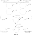
- 28a and 28b are two optical waveguides
- 26 is a microring resonant cavity
- a transmission direction of an optical signal in the microring resonant cavity is a counterclockwise direction.
- the waveguide 28a is connected to an optical network, and an optical signal is transmitted from right to left in the waveguide 28a.
- an optical signal that has a same wavelength as a resonant wavelength of the microring resonant cavity is extracted, and enters the waveguide 28b by passing through the microring resonant cavity.
- a transmission direction of the optical signal in the waveguide 28b is from left to right, and an extraction of the optical signal is completed.
- an optical signal that has a different wavelength from the resonant wavelength of the microring resonant cavity is not affected, and is still transmitted from right to left in the waveguide 28a.
- the waveguide 28b is connected to an optical network node on which the optical add/drop multiplexer is located, which is equivalent to that the waveguide 28b is connected to a local optical network node.
- An optical signal that needs to be inserted is transmitted from left to right in the waveguide 28b, and an optical signal that has a same wavelength as the resonant wavelength of the microring resonant cavity enters the waveguide 28a by passing through the microring resonant cavity.
- a transmission direction of the optical signal in the waveguide 28a is from right to left, and an insertion of the optical signal is completed.
- the extraction means that an optical network signal in the optical network is downloaded to the optical network node on which the optical add/drop multiplexer is located; and the insertion means that an optical network signal on the optical network node on which the optical add/drop multiplexer is located is uploaded to the optical network.
- a disadvantage in the prior art is that the optical add/drop multiplexer supports normal operation only in a single direction. As shown in FIG. 1 , when an optical signal in the waveguide 28a is transmitted from right to left, it can be only set that, in the waveguide 28b, an inserted optical signal enters from the left, and an extracted optical signal goes out from the right. However, this setting further causes a limitation that transmission of an optical signal from left to right is not supported in the waveguide 28a; otherwise, an optical signal in this direction is also extracted by the microring resonant cavity.
- a scenario is considered: Referring to FIG. 2A , for example, there are three optical network nodes: a node 1, a node 2, and a server node 3.
- the node 1, the node 2, and the server node 3 implement optical communication by using an optical waveguide 4. Therefore, optical network signals in two directions need to be transmitted in the optical waveguide 4.
- the optical add/drop multiplexer shown in FIG. 1 is disposed on the node 2, and therefore an optical network signal that is sent by the server node 3 to the node 2 and has a specific wavelength may be extracted by the optical add/drop multiplexer on the node 2.
- optical network signals sent by the node 1 to the server node 3 also include an optical network signal having the specific wavelength
- the optical add/drop multiplexer on the node 2 also extracts the optical network signal that is sent by the node 1 to the server node 3 and has the specific wavelength.
- the server node 3 cannot receive the optical network signal, thereby affecting a normal service processing process.
- WO2007014218 discloses a 2-stage single-directional OADM involving micro-ring resonant cavities.
- Embodiments of the present invention provide an optical add/drop multiplexer and an optical network signal transmission method, so as to resolve a technical problem that the optical add/drop multiplexer supports optical signal transmission only in a single direction.
- an optical add/drop multiplexer including:
- the optical add/drop multiplexer further includes a sixth waveguide (401), which is connected to a second end (e) of the second optical circulator (308), and configured to transmit, to the second optical circulator (308), a third optical network signal that is to be inserted into the first waveguide (301) and whose wavelength is the first wavelength;
- the second optical circulator (308) is further configured to receive the third optical network signal from the sixth waveguide (401), and transmit the third optical network signal to the first optical circulator (305);
- the first optical circulator (305) is further configured to receive the third optical network signal transmitted by the second optical circulator (308), and transmit the third optical network signal to the first microring resonant cavity (302) by using the second waveguide (306);
- the first microring resonant cavity (302) is further configured to receive the third optical network signal transmitted by the first optical circulator (305), and transmit the third optical network signal to the first waveguide (301), where a transmission direction of the third optical network signal in the
- the optical add/drop multiplexer further includes an optical detector (501), which is connected to an end at which the second waveguide (304) is coupled with the first microring resonant cavity (302), and configured to receive an optical network signal that is from the second optical circulator (308) and whose wavelength is the first wavelength, when the resonant wavelength of the first microring resonant cavity (302) deviates from the first wavelength.
- an optical detector 501
- the optical detector is connected to an end at which the second waveguide (304) is coupled with the first microring resonant cavity (302), and configured to receive an optical network signal that is from the second optical circulator (308) and whose wavelength is the first wavelength, when the resonant wavelength of the first microring resonant cavity (302) deviates from the first wavelength.
- the optical detector (501) is a photomultiplier, a pyroelectric detector, or a semiconductor optical detector.
- a fourth possible implementation manner of the first aspect there are multiple first microring resonant cavities (302); where the multiple first microring resonant cavities (302) are arranged in a column, whose ends are separately coupled, a first microring resonant cavity (302) arranged in the first place is coupled with the first side of the first waveguide (301), and a first microring resonant cavity (302) arranged in the last place is coupled with the second waveguide (304).
- a fifth possible implementation manner of the first aspect there are multiple second microring resonant cavities (303); where the multiple second microring resonant cavities (303) are arranged in a column, whose ends are separately coupled, a second microring resonant cavity (303) arranged in the first place is coupled with the first side of the first waveguide (301), and a second microring resonant cavity (303) arranged in the last place is coupled with the third waveguide (306).
- the optical network is a wavelength division multiplexing WDM optical network.
- an optical network signal transmission method including:
- the method further includes:
- the method further includes: if the resonant wavelength of the first microring resonant cavity (302) is not the first wavelength, receiving, by using an optical detector (501) in the optical add/drop multiplexer, the third optical network signal transmitted by the first waveguide (301), where the optical detector (501) is connected to an end at which the second waveguide (304) is coupled with the first microring resonant cavity (302).
- the second direction is a specified transmission direction of a to-be-processed optical network signal, that is, the optical add/drop multiplexer needs to insert or extract an optical network signal transmitted in the second direction.
- the optical add/drop multiplexer needs to insert or extract an optical network signal transmitted in the second direction.
- normal transmission should be ensured.
- the first microring resonant cavity 302 receives the first optical network signal from the first waveguide 301, and transmits the first optical network signal to the second microring resonant cavity 303 by using the first optical circulator 305; the second microring resonant cavity 303 retransmits the first optical network signal to the first waveguide 301 in a coupling manner, and the first optical network signal continues to be transmitted in the first waveguide 301 in the first direction.
- the second microring resonant cavity 303 receives the second optical network signal, and extracts and distributes, by using the second optical circulator 308 and the first optical circulator 305, the second optical network signal to the optical network node on which the optical add/drop multiplexer is located.
- an optical network signal in the first direction is not extracted, and can be still normally transmitted; however, an optical network signal in the second direction can be extracted and distributed to the optical network node, thereby ensuring not only normal extraction operation of the optical add/drop multiplexer but also that when inserting or extracting an optical signal in one direction, the optical add/drop multiplexer can support normal transmission of an optical signal in the other direction, so that all optical network signals transmitted in two directions can be properly processed, so as to ensure normal optical communication.
- system and “network” may be used interchangeably in this specification.
- network may be used interchangeably in this specification.
- the term “and/or” in this specification describes only an association relationship for describing associated objects and represents that three relationships may exist. For example, A and/or B may represent the following three cases: Only A exists, both A and B exist, and only B exists.
- the character “/” in this specification generally indicates an “or” relationship between the associated objects.
- FIG. 2B in the network structure of FIG. 2A that continues to be used as an example, for example, there are three optical network nodes: a node 1, a node 2, and a server node 3.
- the node 1, the node 2, and the server node 3 implement optical communication by using an optical waveguide 4. Therefore, optical network signals in two directions need to be transmitted in the optical waveguide 4.
- an optical add/drop multiplexer disposed on the node 2 in FIG. 2B is not the optical add/drop multiplexer in the prior art but an optical add/drop multiplexer provided in an embodiment of the present invention.
- optical network signals sent by the node 1 to the server node 3 also include an optical network signal having the specific wavelength, and the optical add/drop multiplexer in this embodiment of the present invention disposed on the node 2 does not extract the optical network signal that is sent by the node 1 to the server node 3 and has the specific wavelength, which can be normally received by the server node 3. Therefore, normal optical signal transmission is ensured, and a normal service processing process is not affected as much as possible.
- FIG. 2B may be considered as a possible application scenario of the present invention.
- the following describes the optical add/drop multiplexer in this embodiment of the present invention in detail with reference to the accompanying drawings, that is, the optical add/drop multiplexer disposed on the node 2 in FIG. 2B .
- an embodiment of the present invention provides an optical add/drop multiplexer.
- the optical add/drop multiplexer may include a first microring resonant cavity 302, a second microring resonant cavity 303, a second waveguide 304, a first optical circulator 305, a third waveguide 306, a fourth waveguide 307, a second optical circulator 308, and a fifth waveguide 309.
- a first waveguide 301 in FIG. 3 belongs to an optical network, which is also indicated in FIG. 3 that the first waveguide 301 is connected to the optical network.
- the first microring resonant cavity 302 is coupled with a first side of the first waveguide 301 that is in the optical network and that is configured to transmit an optical network signal; and is configured to receive, from the first waveguide 301, an optical network signal whose wavelength is a first wavelength.
- the optical network signal herein is referred to as a first optical network signal.
- a resonant wavelength of the first microring resonant cavity 302 is the first wavelength. Therefore, the first microring resonant cavity 302 can receive the first optical network signal from the first waveguide 301 in a coupling manner.
- the second microring resonant cavity 303 is also coupled with the first side of the first waveguide 301, that is, the first microring resonant cavity 302 and the second microring resonant cavity 303 are located on a same side of the first waveguide 301.
- the second microring resonant cavity 303 is configured to receive the first optical network signal transmitted by the first microring resonant cavity 302, and may retransmit the first optical network signal to the first waveguide 301, where a transmission direction of the first optical network signal in the first waveguide 301 is always a first direction.
- the second microring resonant cavity 303 may further receive, from the first waveguide 301, an optical network signal whose wavelength is also the first wavelength and whose transmission direction in the first waveguide 301 is a second direction.
- the optical network signal herein is referred to as a second optical network signal, the second direction is opposite to the first direction, and the second direction is a specified direction of a to-be-processed optical network signal transmitted in the first waveguide 301, that is, processing such as an extraction may be performed on an optical network signal in the second direction.
- processing such as an extraction may be performed on an optical network signal in the second direction.
- a signal in the first direction normal transmission of the signal in the first waveguide 301 needs to be ensured, and the signal is not extracted or distributed to an optical network node on which the optical add/drop multiplexer is located.
- a resonant wavelength of the second microring resonant cavity 303 is also the first wavelength. Therefore, the second microring resonant cavity 303 can receive the first optical network signal, and may transmit the first optical network signal to the first waveguide 301 in a coupling manner; and the second microring resonant cavity 303 can receive the second optical network signal from the first waveguide 301 in a coupling manner.
- One end of the second waveguide 304 is coupled with the first microring resonant cavity 302, and the other end of the second waveguide 304 is connected to a first end a of the first optical circulator 305.
- a second end b of the first optical circulator 305 is connected to one end of the third waveguide 306, and the other end of the third waveguide 306 is coupled with the second microring resonant cavity 303.
- a third end c of the first optical circulator 305 is connected to one end of the fourth waveguide 307, and the other end of the fourth waveguide 307 is connected to a third end f of the second optical circulator 308.
- the first optical circulator 305 is configured to transmit, to the second microring resonant cavity 303, the first optical network signal transmitted by the first microring resonant cavity 302, that is, the first microring resonant cavity 302 receives the first optical network signal from the first waveguide 301 in a coupling manner, and transmits the first optical network signal to the first optical circulator 305 by using the second waveguide 304.
- the first optical network signal enters from the first end a of the first optical circulator 305, goes out from the second end b of the first optical circulator 305, reaches the second microring resonant cavity 303 by passing through the third waveguide 306, and then, is transmitted to the first waveguide 301 by coupling the second microring resonant cavity 303 with the first waveguide 301.
- the transmission direction of the first optical network signal in the first waveguide 301 is the first direction.
- the transmission direction is still the first direction. It can be learned that, after passing through the optical add/drop multiplexer, optical network signals that have various wavelengths and that are included in optical network signals in a specified direction in which no processing should be performed are not lost, and are still normally transmitted in an original direction, which is not affected.
- the first optical circulator 305 is further configured to receive the second optical network signal transmitted by the second microring resonant cavity 303.
- the second optical network signal enters from the second end b of the first optical circulator 305, goes out from the third end c of the first optical circulator 305, and enters the second optical circulator 308 by using the fourth waveguide 307.
- a first end d of the second optical circulator 308 is connected to one end of the fifth waveguide 309.
- the second optical circulator 308 is configured to receive the second optical network signal transmitted by the first optical circulator 305, and extracts the second optical network signal locally by using the fifth waveguide 309.
- the second optical network signal enters from the third end f of the second optical circulator 308, goes out from the first end d of the second optical circulator 308, and is extracted locally by passing through the fifth waveguide 309.
- transmission directions of optical signals in the first optical circulator 305 and the second optical circulator 308 are both counterclockwise directions, which are used as an example and are shown as arrows in the first optical circulator 305 and the second optical circulator 308 in FIG. 3 .
- the other end of the fifth waveguide 309 is connected to the optical network node, that is, the optical network node on which the optical add/drop multiplexer is located. It may be considered that the other end of the fifth waveguide 309 is locally connected.
- an optical network signal that should not be processed in the first direction is not extracted, and can be still normally transmitted; however, a specified optical network signal that needs to be processed in the second direction can be extracted locally, that is, extracted and distributed to the optical network node on which the optical add/drop multiplexer is located, thereby ensuring not only normal extraction operation of the optical add/drop multiplexer but also that when inserting or extracting an optical signal in one direction, the optical add/drop multiplexer can support normal transmission of an optical signal in the other direction, so that all optical network signals transmitted in two directions can be properly processed without mutual interference.
- a second end e of the second optical circulator 308 may be further connected to a sixth waveguide 401, and the sixth waveguide 401 is configured to transmit, to the second optical circulator 308, a third optical network signal that is to be inserted into the first waveguide 301, where a wavelength of the third optical network signal is also the first wavelength. Only an optical network signal that has a same wavelength as a resonant wavelength of a corresponding microring resonant cavity can be extracted or inserted.
- the second optical circulator 308 is further configured to receive the third optical network signal from the sixth waveguide 401, and transmit the third optical network signal to the first optical circulator 305.
- the third optical network signal enters from the second end e of the second optical circulator 308, and goes out from the third end f of the second optical circulator 308.
- the first optical circulator 305 is further configured to receive the third optical network signal transmitted by the second optical circulator 308, and transmit the third optical network signal to the first microring resonant cavity 302 by using the second waveguide 304.
- the third optical network signal enters from the third end f of the first optical circulator 305, and goes out from the first end d of the first optical circulator 305.
- the first microring resonant cavity 302 is further configured to receive the third optical network signal transmitted by the first optical circulator 305, and transmit the third optical network signal to the first waveguide 301 in a coupling manner. After the third optical network signal is transmitted to the first waveguide 301, a transmission direction of the third optical network signal in the first waveguide 301 is the second direction.
- the to-be-inserted third optical network signal enters the second end e of the second optical circulator 308 by using the sixth waveguide 401, goes out from the third end f of the second optical circulator 308, enters the third end c of the first optical circulator 305, goes out from the first end a of the first optical circulator 305, and enters the first microring resonant cavity 302 by passing through the second waveguide 304, and the first microring resonant cavity 302 transmits the third optical network signal to the first waveguide 301 in a coupling manner. Therefore, an insertion of the optical network signal is completed.
- both an insertion and an extraction of an optical network signal can be normally performed, and signals in two transmission directions do not interfere with each other.
- resonant wavelengths of two microring resonant cavities are set to ⁇ 3, that is, the first wavelength is ⁇ 3.
- Optical transmission directions of two optical circulators are counterclockwise directions. The first direction is set to a right-to-left direction in the first waveguide 301, and the second direction is a left-to-right direction in the first waveguide 301.
- an optical network signal whose wavelength is ⁇ 3 is extracted by the second microring resonant cavity 303, and enters an extraction end of the optical add/drop multiplexer by passing through the first optical circulator 305 and the second optical circulator 308, that is, enters the fifth waveguide 309; however, an optical network signal having another wavelength is not affected by the second microring resonant cavity 303 and the first microring resonant cavity 302, and continues to be transmitted in the first waveguide 301, that is, directly passes through the optical add/drop multiplexer.
- an optical network signal whose wavelength is ⁇ 3 is extracted by the first microring resonant cavity 302, but after passing through the first optical circulator 305, the optical network signal reenters the network by passing through the second microring resonant cavity 303, that is, enters the first waveguide 301, thereby avoiding damage caused by the optical add/drop multiplexer on the optical network signal that is transmitted in a right-to-left direction and whose wavelength is ⁇ 3; however, an optical network signal having another wavelength is not affected by the second microring resonant cavity 303 and the first microring resonant cavity 302, and continues to be transmitted in the first waveguide 301, that is, directly passes through the optical add/drop multiplexer.
- an optical network signal whose wavelength is ⁇ 3 enters the optical add/drop multiplexer at an insertion end (that is, an end of the sixth waveguide 401), and is inserted into the network by the first microring resonant cavity 302 by passing through the second optical circulator 308 and the first optical circulator 305, that is, inserted into the first waveguide 301, and a transmission direction of the optical network signal is from left to right.
- An insertion process and an extraction process in this embodiment of the present invention may be simultaneously performed, and are not affected by each other.
- an optical detector 501 is connected to an end at which the second waveguide 304 is coupled with the first microring resonant cavity 302, and is configured to monitor an inserted optical network signal.
- the optical detector 501 is configured to: when the resonant wavelength of the first microring resonant cavity 302 deviates from the first wavelength, receive an optical network signal that is from the second optical circulator 305 and whose wavelength is the first wavelength.
- shapes of the second waveguide 304 and the third waveguide 306 in FIG. 3 to FIG. 5 are all arcs, which are only drawings herein and do not represent actual shapes. Actual shapes of the second waveguide 304 and the third waveguide 306 may be arcs, or may be straight lines, which are not limited in the present invention.
- resonant wavelengths of the first microring resonant cavity 302 and the second microring resonant cavity 303 are ⁇ 3, which continues to be used as an example.
- the optical add/drop multiplexer When the optical add/drop multiplexer is being initialized or enters an operating state, light whose wavelength is ⁇ 3 is first incident at the insertion end.
- the resonant wavelength of the first microring resonant cavity 302 deviates from ⁇ 3, for example, deviates to a second wavelength, this beam of light whose wavelength is ⁇ 3 is not inserted into the optical network, but received by the optical detector 501. Therefore, the resonant wavelength of the first microring resonant cavity 302 may be adjusted by using the thermo-optic effect.
- the resonant wavelength of the first microring resonant cavity 302 is adjusted to a proper resonant wavelength.
- the optical add/drop multiplexer After the resonant wavelength of the first microring resonant cavity 302 is adjusted to the proper resonant wavelength (for example, ⁇ 3), the optical add/drop multiplexer enters the operating state. If the resonant wavelength of the second microring resonant cavity 303 also deviates from ⁇ 3, an optical network signal that is transmitted from left to right in the first waveguide 301 and whose wavelength is ⁇ 3 is not extracted by the second microring resonant cavity 303 but extracted by the first microring resonant cavity 302, and enters the optical detector 501 after being transmitted in a clockwise direction in the first microring resonant cavity 302.
- the proper resonant wavelength for example, ⁇ 3
- the optical detector 501 may be used not only to adjust the resonant wavelength of the first microring resonant cavity 302 but also to adjust the resonant wavelength of the second microring resonant cavity 303. Therefore, only one optical detector 501 needs to be disposed, thereby saving a hardware resource.
- the optical detector 501 may be specifically a photomultiplier, a pyroelectric detector, a semiconductor optical detector, or the like.
- first microring resonant cavities 302 there may be one or more first microring resonant cavities 302, and there may be an even number or an odd number of first microring resonant cavities 302.
- first microring resonant cavity 302 which is used as an example. If there are multiple first microring resonant cavities 302, the multiple first microring resonant cavities 302 are arranged in a column, whose ends are separately coupled, a first microring resonant cavity 302 arranged in the first place is coupled with the first side of the first waveguide 301, and a first microring resonant cavity 302 arranged in the last place is coupled with the second waveguide 304.
- first microring resonant cavities 302 there are two first microring resonant cavities 302, which is used as an example.
- FIG. 3 to FIG. 5 there is one second microring resonant cavity 303, which is used as an example. If there are multiple second microring resonant cavities 303, the multiple second microring resonant cavities 303 are arranged in a column, whose ends are separately coupled, a second microring resonant cavity 303 arranged in the first place is coupled with the first side of the first waveguide 301, and a second microring resonant cavity 303 arranged in the last place is coupled with the third waveguide 306.
- FIG. 6B there are two second microring resonant cavities 303, which is used as an example.
- a size of the first microring resonant cavity 302 is different from that of the second microring resonant cavity 303, which is merely for ease of drawing and does not represent actual sizes of the first microring resonant cavity 302 and the second microring resonant cavity 303. That is, actually, the size of the first microring resonant cavity 302 may be the same as or different from that of the second microring resonant cavity 303, and this is not limited in this embodiment of the present invention.
- a person skilled in the art may understand that different variants in a specific implementation process of this embodiment of the present invention also fall within the protection scope of the present invention.
- first microring resonant cavities 302 there are two first microring resonant cavities 302 and two second microring resonant cavities 303, which is used as an example. It should be noted that a quantity of first microring resonant cavities 302 may be equal or not equal to a quantity of second microring resonant cavities 303. An example in which the quantities are not equal is used in FIG. 6A and FIG. 6B , and an example in which the quantities are equal is used in FIG. 6C , and FIG. 3 to FIG. 5 .
- a wavelength range of an extracted optical network signal is broader, that is, a wavelength passband is flatter, but another wavelength is not affected. In this way, it is easier to perform fine adjustment on a resonant wavelength of a microring resonant cavity.
- resonant wavelengths of entireties that include these microring resonant cavities need to be the same. That is, whether how many the quantity of first microring resonant cavities 302 and the quantity of second microring resonant cavities 303 are, if the first microring resonant cavities 302 and the second microring resonant cavities 303 are considered as two entireties, a resonant wavelength of the first microring resonant cavities 302 as an entirety needs to be the same as a resonant wavelength of the second microring resonant cavities 303 as an entirety.
- resonant wavelengths of all the first microring resonant cavities 302 may be set to be the same, which is also applicable to the second microring resonant cavities 303. That is, for the optical add/drop multiplexer, whether how many microring resonant cavities the optical add/drop multiplexer includes, resonant wavelengths of all the microring resonant cavities may be the same.
- the optical network may refer to a WDM optical network.
- FIG. 7A and FIG. 7B based on a same invention concept, an embodiment of the present invention provides an optical network signal transmission method.
- FIG. 7A and FIG. 7B show a method for transmitting an optical network signal by using an optical add/drop multiplexer, and the optical add/drop multiplexer may be the optical add/drop multiplexer shown in FIG. 3 to FIG. 6C .
- Step 701 Receive, by using a first microring resonant cavity in the optical add/drop multiplexer, a first optical network signal transmitted by a first waveguide in an optical network, where the first microring resonant cavity is coupled with a first side of the first waveguide, a wavelength of the first optical network signal is a first wavelength, and a transmission direction of the first optical network signal in the first waveguide is a first direction.
- the first optical network signal is transmitted in the first waveguide 301, the transmission direction of the first optical network signal is the first direction, and the first direction is a specified transmission direction in which the optical add/drop multiplexer should not perform processing, that is, the optical add/drop multiplexer should not extract an optical network signal transmitted in this direction.
- a resonant wavelength of the first microring resonant cavity 302 is the first wavelength. Therefore, the first microring resonant cavity 302 can receive the first optical network signal in the first waveguide 301 in a coupling manner. However, the first microring resonant cavity 302 cannot receive an optical network signal that has another wavelength and that is transmitted in the first waveguide 301.
- Step 702 Receive, by using a first optical circulator in the optical add/drop multiplexer, the first optical network signal transmitted by the first microring resonant cavity by using a second waveguide, where the first optical circulator is connected to one end of the second waveguide, and the other end of the second waveguide is coupled with the first microring resonant cavity.
- the first microring resonant cavity 302 After receiving the first optical network signal, the first microring resonant cavity 302 transmits the first optical network signal to the first optical circulator 305 by using the second waveguide 304.
- Step 703 Receive, by using a second microring resonant cavity in the optical add/drop multiplexer, the first optical network signal transmitted by the first optical circulator by using a third waveguide, where the first optical circulator is connected to one end of the third waveguide, the other end of the third waveguide is coupled with the second microring resonant cavity, and the first wavelength is a resonant wavelength of the first microring resonant cavity and the second microring resonant cavity.
- the first optical circulator 305 After receiving the first optical network signal transmitted by the first microring resonant cavity 302, the first optical circulator 305 transmits the first optical network signal to the second microring resonant cavity 303 by using the third waveguide 306.
- a wavelength of the second microring resonant cavity 303 is also the first wavelength. Therefore, the second microring resonant cavity 303 can receive the first optical network signal.
- Step 704 Retransmit the first optical network signal to the first waveguide by using the second microring resonant cavity, so that an optical network signal in the first direction is transmitted in the first waveguide.
- the second microring resonant cavity 303 may retransmit the first optical network signal to the first waveguide 301 in a coupling manner, so that the first optical network signal may continue to be transmitted in the first waveguide 301 in the first direction. It can be learned that after passing through the optical add/drop multiplexer, an optical network signal that should not be processed by the optical add/drop multiplexer is not changed, and continues to be normally transmitted.
- Step 705 Receive, by using the second microring resonant cavity, the second optical network signal transmitted by the first waveguide, and transmit the second optical network signal to the first optical circulator by using the third waveguide, where a wavelength of the second optical network signal is the first wavelength, a transmission direction of the second optical network signal in the first waveguide is a second direction, the second direction is a specified direction of a to-be-processed optical network signal transmitted in the first waveguide, and the second direction is opposite to the first direction.
- the first waveguide 301 may transmit an optical network signal in the second direction opposite to the first direction.
- the second optical network signal that has a same wavelength as the first wavelength is transmitted in the first waveguide 301, and the transmission direction of the second optical network signal in the first waveguide 301 is the second direction.
- Step 706 Receive, by using the first optical circulator, the second optical network signal transmitted by the second microring resonant cavity, and transmit the second optical network signal to a second optical circulator in the optical add/drop multiplexer.
- Step 707 Receive, by using the second optical circulator, the second optical network signal transmitted by the first optical circulator, and extract and distribute, by using a fifth waveguide connected to a first end of the second optical circulator, the second optical network signal to an optical network node on which the optical add/drop multiplexer is located, where a third end of the second optical circulator is connected to one end of a fourth waveguide, and the other end of the fourth waveguide is connected to a third end of the first optical circulator.
- Step 701 to step 704 describe a process of filtering an optical network signal (a process that, after going out from the first waveguide 301, the first optical network signal reenters the first waveguide 301 by passing through the first microring resonant cavity 302, the second waveguide 304, the first optical circulator 305, the third waveguide 306, and the second microring resonant cavity 303, which is referred to as filtration of an optical network signal), and step 705 to step 707 describe a process of extracting an optical network signal.
- step 701 to step 704 are considered as a whole process, and step 705 to step 707 are considered as a whole process, the two whole processes may be executed in any sequence, which is not limited by step numbers. That is, in this embodiment of the present invention, two processes of an extraction of a signal and filtration of a signal may be simultaneously performed, or may be performed in any sequence, and do not interfere with each other.
- the second direction is a specified transmission direction of a signal that needs to be processed. Therefore, if a wavelength of an optical network signal transmitted in this direction is the same as a wavelength of a microring resonant cavity in the optical add/drop multiplexer, the optical network signal needs to be locally extracted, that is, extracted and distributed to the optical network node on which the optical add/drop multiplexer is located.
- the second optical network signal is transmitted by using the first waveguide 301, and the transmission direction of the second optical network signal is the second direction.
- the second microring resonant cavity 303 receives, in a coupling manner, the second optical network signal transmitted in the first waveguide 301, and may transmit the second optical network signal to the first optical circulator 305 by using the third waveguide 306.
- the first optical circulator 305 transmits the second optical network signal to the second optical circulator 308 by using the fourth waveguide 307.
- the second optical circulator 308 extracts the second optical network signal locally by using the fifth waveguide 309. Therefore, an extraction of the signal is completed.
- the method further includes: Step 801: Receive a third optical network signal from the optical network node by using the second optical circulator, where the third end of the second optical circulator is connected to the one end of the fourth waveguide, the other end of the fourth waveguide is connected to the third end of the first optical circulator, a second end of the second optical circulator is connected to a sixth waveguide, and the sixth waveguide is configured to transmit the local third optical network signal to the second optical circulator.
- Step 802 Receive, by using the first optical circulator, the third optical network signal transmitted by the second optical circulator, and transmit the third optical network signal to the second waveguide. If the resonant wavelength of the first microring resonant cavity is the first wavelength, step 803 is performed; or if the resonant wavelength of the first microring resonant cavity is not the first wavelength, step 804 is performed.
- Step 803 If the resonant wavelength of the first microring resonant cavity is the first wavelength, the first microring resonant cavity receives the third optical network signal transmitted by the second waveguide, and transmits the first optical network signal to the first waveguide, where a transmission direction of the third optical network signal in the first waveguide is the second direction.
- Steps 801 to 803 describe an insertion process of a signal, that is, an optical network signal in the optical network node is inserted into the optical network.
- the to-be-inserted third optical network signal is received by using the sixth waveguide 401, and the third optical network signal is transmitted to the second optical circulator 308; after receiving the third optical network signal, the second optical circulator 308 transmits the third optical network signal to the first optical circulator 305 by using the fourth waveguide 307; after the first optical circulator 305 receives the third optical network signal, if the resonant wavelength of the first microring resonant cavity 302 does not deviate from the first wavelength, the first optical circulator 305 may transmit the third optical network signal to the first microring resonant cavity 302 by using the second waveguide 304, and the first microring resonant cavity 302 transmits the third optical network signal to the first waveguide 301 in a coupling manner. Therefore, the insertion of the signal is completed.
- processes of an extraction of a signal, filtration of a signal, and an insertion of a signal may be simultaneously performed, or may be performed in any sequence, and do not interfere with each other.
- the method may further include: Step 804: If the resonant wavelength of the first microring resonant cavity is not the first wavelength, receive, by using an optical detector in the optical add/drop multiplexer, the third optical network signal transmitted by the first waveguide, where the optical detector is connected to an end at which the second waveguide is coupled with the first microring resonant cavity.
- the resonant wavelength of the first microring resonant cavity 302 may be adjusted by using a thermo-optic effect.
- the resonant wavelength of the first microring resonant cavity 302 is adjusted to a proper resonant wavelength.
- this embodiment of the present invention provides an optical add/drop multiplexer, including: a first microring resonant cavity 302, coupled with a first side of a first waveguide 301 in an optical network, and configured to receive, from the first waveguide 301, a first optical network signal whose wavelength is a first wavelength; a second microring resonant cavity 303, coupled with the first side of the first waveguide 301, and configured to receive the first optical network signal transmitted by the first microring resonant cavity 302, and transmit the first optical network signal to the first waveguide 301, where a transmission direction of the first optical network signal in the first waveguide 301 is a first direction; and configured to receive, from the first waveguide 301, a second optical network signal whose wavelength is the first wavelength and whose transmission direction in the first waveguide 301 is a second direction, where the first wavelength is a resonant wavelength of the first microring resonant cavity 302 and the second microring resonant cavity 303, the second direction is a specified
- the second direction is a specified transmission direction of a to-be-processed optical network signal, that is, the optical add/drop multiplexer needs to insert or extract an optical network signal transmitted in the second direction.
- the optical add/drop multiplexer needs to insert or extract an optical network signal transmitted in the second direction.
- normal transmission should be ensured.
- the first microring resonant cavity 302 receives the first optical network signal from the first waveguide 301, and transmits the first optical network signal to the second microring resonant cavity 303 by using the first optical circulator 305; the second microring resonant cavity 303 retransmits the first optical network signal to the first waveguide 301 in a coupling manner, and the first optical network signal continues to be transmitted in the first waveguide 301 in the first direction.
- the second microring resonant cavity 303 receives the second optical network signal, and extracts and distributes, by using the second optical circulator 308 and the first optical circulator 305, the second optical network signal to the optical network node on which the optical add/drop multiplexer is located.
- an optical network signal in the first direction is not extracted, and can be still normally transmitted; however, an optical network signal in the second direction can be extracted and distributed to the optical network node, thereby ensuring not only normal extraction operation of the optical add/drop multiplexer but also that when inserting or extracting an optical signal in one direction, the optical add/drop multiplexer can support normal transmission of an optical signal in the other direction, so that all optical network signals transmitted in two directions can be properly processed, so as to ensure normal optical communication.
- the disclosed system, apparatus, and method may be implemented in other manners.
- the described apparatus embodiment is merely an example.
- the module or unit division is merely logical function division and may be other division in actual implementation.
- a plurality of units or components may be combined or integrated into another system, or some features may be ignored or not performed.
- the displayed or discussed mutual couplings or direct couplings or communication connections may be implemented by using some interfaces.
- the indirect couplings or communication connections between the apparatuses or units may be implemented in electronic, mechanical, or other forms.
- the units described as separate parts may or may not be physically separate, and parts displayed as units may or may not be physical units, may be located in one position, or may be distributed on a plurality of network units. Some or all of the units may be selected according to actual needs to achieve the objectives of the solutions of the embodiments.
- functional units in the embodiments of the present application may be integrated into one processing unit, or each of the units may exist alone physically, or two or more units are integrated into one unit.
- the integrated unit may be implemented in a form of hardware, or may be implemented in a form of a software functional unit.
- the integrated unit When the integrated unit is implemented in the form of a software functional unit and sold or used as an independent product, the integrated unit may be stored in a computer-readable storage medium. Based on such an understanding, the technical solutions of the present application essentially, or the part contributing to the prior art, or all or a part of the technical solutions may be implemented in the form of a software product.
- the software product is stored in a storage medium and includes several instructions for instructing a computer device (which may be a personal computer, a server, or a network device) or a processor to perform all or a part of the steps of the methods described in the embodiments of the present application.
- the foregoing storage medium includes: any medium that can store program code, such as a USB flash drive, a removable hard disk, a read-only memory (ROM, Read-Only Memory), a random access memory (RAM, Random Access Memory), a magnetic disk, or an optical disc.
- program code such as a USB flash drive, a removable hard disk, a read-only memory (ROM, Read-Only Memory), a random access memory (RAM, Random Access Memory), a magnetic disk, or an optical disc.
Landscapes
- Engineering & Computer Science (AREA)
- Computer Networks & Wireless Communication (AREA)
- Signal Processing (AREA)
- Computing Systems (AREA)
- Physics & Mathematics (AREA)
- Electromagnetism (AREA)
- Optical Communication System (AREA)
- Optical Integrated Circuits (AREA)
- Optical Modulation, Optical Deflection, Nonlinear Optics, Optical Demodulation, Optical Logic Elements (AREA)
Claims (10)
- Optischer Add/Drop-Multiplexer, umfassend:einen ersten Mikroring-Resonanzhohlraum (302), der mit einer ersten Seite eines ersten Wellenleiters (301) in einem optischen Netzwerk gekoppelt und konfiguriert ist, um, von dem ersten Wellenleiter (301), ein erstes optisches Netzwerksignal zu empfangen, dessen Wellenlänge eine erste Wellenlänge ist;einen zweiten Mikroring-Resonanzhohlraum (303), der mit der ersten Seite des ersten Wellenleiters (301) gekoppelt und konfiguriert ist, um das durch den ersten Mikroring-Resonanzhohlraum (302) übertragene erste optische Netzwerksignal zu empfangen und das erste optische Netzwerksignal an den ersten Wellenleiter (301) zu übertragen, wobei eine Übertragungsrichtung des ersten optischen Netzwerksignals in dem ersten Wellenleiter (301) eine erste Richtung ist; undkonfiguriert ist, um, von dem ersten Wellenleiter (301), ein zweites optisches Netzwerksignal zu empfangen, dessen Wellenlänge die erste Wellenlänge ist und dessen Übertragungsrichtung in dem ersten Wellenleiter (301) eine zweite Richtung ist, wobei die erste Wellenlänge eine Resonanzwellenlänge des ersten Mikroring-Resonanzhohlraums (302) und des zweiten Mikroring-Resonanzhohlraums (303) ist, wobei die zweite Richtung eine spezifizierte Richtung eines zu verarbeitenden optischen Netzwerksignals ist, das in dem ersten Wellenleiter (301) übertragen wird, und die zweite Richtung der ersten Richtung entgegengesetzt ist;einen ersten optischen Zirkulator (305), wobei ein erstes Ende (a) des ersten optischen Zirkulators (305) mit einem Ende eines zweiten Wellenleiters (304) verbunden ist, und ein zweites Ende (b) des ersten optischen Zirkulators (305) mit einem Ende eines dritten Wellenleiters (306) verbunden ist; konfiguriert ist, um, an den zweiten Mikroring-Resonanzhohlraum (303), das durch den ersten Mikroring-Resonanzhohlraum (302) übertragene erste optische Netzwerksignal zu übertragen und das durch den zweiten Mikroring-Resonanzhohlraum (303) übertragene zweite optische Netzwerksignal zu empfangen; wobeidas andere Ende des zweiten Wellenleiters (304) mit dem ersten Mikroring-Resonanzhohlraum (302) gekoppelt ist; unddas andere Ende des dritten Wellenleiters (306) mit dem zweiten Mikroring-Resonanzhohlraum (303) gekoppelt ist; undeinen zweiten optischen Zirkulator (308), wobei ein drittes Ende (f) des zweiten optischen Zirkulators (308) unter Verwendung eines vierten Wellenleiters (307) mit einem dritten Ende (c) des ersten optischen Zirkulators (305) verbunden ist, und ein erstes Ende (d) des zweiten optischen Zirkulators (308) mit einem Ende eines fünften Wellenleiters (309) verbunden ist; konfiguriert ist, um das von dem ersten optischen Zirkulator (305) gesendete zweite optische Netzwerksignal zu empfangen und unter Verwendung des fünften Wellenleiters (309) das zweite optische Netzwerksignal an einem optischen Netzwerkknoten zu extrahieren und zu verteilen, auf dem sich der optische Add/Drop-Multiplexer befindet.
- Optischer Add/Drop-Multiplexer nach Anspruch 1, wobei der optische Add/Drop-Multiplexer ferner einen sechsten Wellenleiter (401) umfasst, der mit einem zweiten Ende (e) des zweiten optischen Zirkulators (308) verbunden ist und konfiguriert ist, um, an den zweiten optischen Zirkulator (308), ein drittes optisches Netzwerksignal zu übertragen, das in den ersten Wellenleiter (301) eingefügt werden soll und dessen Wellenlänge die erste Wellenlänge ist;
der zweite optische Zirkulator (308) ferner konfiguriert ist, um das dritte optische Netzwerksignal von dem sechsten Wellenleiter (401) zu empfangen und das dritte optische Netzwerksignal an den ersten optischen Zirkulator (305) zu übertragen;
der erste optische Zirkulator (305) ferner konfiguriert ist, um das dritte optische Netzwerksignal
zu empfangen, das von dem zweiten optischen Zirkulator (308) übertragen wird, und das dritte optische Netzwerksignal unter Verwendung des zweiten Wellenleiters (306) an den ersten Mikroring-Resonanzhohlraum (302) zu übertragen; und
der erste Mikroring-Resonanzhohlraum (302) ferner konfiguriert ist, um das von dem ersten optischen Zirkulator (305) übertragene dritte optische Netzwerksignal zu empfangen und das dritte optische Netzwerksignal an den ersten Wellenleiter (301) zu übertragen, wobei eine Übertragungsrichtung des dritten optischen Netzwerksignals in dem ersten Wellenleiter (301) die zweite Richtung ist. - Optischer Add/Drop-Multiplexer nach Anspruch 1 oder 2, wobei der optische Add/Drop-Multiplexer ferner einen optischen Detektor (501) umfasst, der mit einem Ende verbunden ist, an dem der zweite Wellenleiter (304) mit der ersten Mikroring-Resonanzhohlraum (302) gekoppelt ist, und konfiguriert ist, um ein optisches Netzwerksignal zu empfangen, das von dem zweiten optischen Zirkulator (308) stammt und dessen Wellenlänge die erste Wellenlänge ist, wenn die Resonanzwellenlänge des ersten Mikroring-Resonanzhohlraums (302) von der ersten Wellenlänge abweicht.
- Optischer Add/Drop-Multiplexer nach Anspruch 3, wobei der optische Detektor (501) ein Fotovervielfacher, ein pyroelektrischer Detektor oder ein optischer Halbleiterdetektor ist.
- Optischer Add/Drop-Multiplexer nach einem der Ansprüche 1 bis 4, wobei mehrere erste Mikroring-Resonanzhohlräume (302) vorhanden sind; wobei die mehreren ersten Mikroring-Resonanzhohlräume (302) in einer Säule angeordnet sind, deren Enden getrennt gekoppelt sind, wobei ein erster Mikroring-Resonanzhohlraum (302), der an der ersten Stelle angeordnet ist, mit der ersten Seite des ersten Wellenleiters (301) gekoppelt ist, und ein erster Mikroring-Resonanzhohlraum (302), der an der letzten Stelle angeordnet ist, mit dem zweiten Wellenleiter (304) gekoppelt ist.
- Optischer Add/Drop-Multiplexer nach einem der Ansprüche 1 bis 5, wobei mehrere zweite Mikroring-Resonanzhohlräume (303) vorhanden sind; wobei die mehreren zweiten Mikroring-Resonanzhohlräume (303) in einer Säule angeordnet sind, deren Enden getrennt gekoppelt sind, wobei ein zweiter Mikroring-Resonanzhohlraum (303), der an der ersten Stelle angeordnet ist, mit der ersten Seite des ersten Wellenleiters (301) gekoppelt ist, und ein zweiter Mikroring-Resonanzhohlraum (303), der an der letzten Stelle angeordnet ist, mit dem dritten Wellenleiter (306) gekoppelt ist.
- Optischer Add/Drop-Multiplexer nach einem der Ansprüche 1 bis 6, wobei das optische Netzwerk ein optisches Wellenlängen-Multiplex(Wavelength Division Multiplex, WDM)-Netzwerk ist.
- Optisches Netzwerk-Signalübertragungsverfahren, umfassend:Empfangen, unter Verwendung eines ersten Mikroring-Resonanzhohlraums (302) in einem optischen Add/Drop-Multiplexer, eines ersten optischen Netzwerksignals, das durch einen ersten Wellenleiter (301) in einem optischen Netzwerk übertragen wird, wobei der erste Mikroring-Resonanzhohlraum (302) mit einer ersten Seite des ersten Wellenleiters (301) gekoppelt ist, eine Wellenlänge des ersten optischen Netzwerksignals eine erste Wellenlänge ist und eine Übertragungsrichtung des ersten optischen Netzwerksignals in dem ersten Wellenleiter (301) eine erste Richtung ist;Empfangen, unter Verwendung eines ersten optischen Zirkulators (305) in dem optischen Add/Drop-Multiplexer, des durch den ersten Mikroring-Resonanzhohlraum (302) unter Verwendung eines zweiten Wellenleiters (304) übertragenen ersten optischen Netzwerksignals, wobei der erste optische Zirkulator (305) mit einem Ende des zweiten Wellenleiters (304) verbunden ist und das andere Ende des zweiten Wellenleiters (304) mit dem ersten Mikroring-Resonanzhohlraum (302) gekoppelt ist;Empfangen, unter Verwendung eines zweiten Mikroring-Resonanzhohlraums (303) in dem optischen Add/Drop-Multiplexer, des durch den ersten optischen Zirkulator (305) unter Verwendung eines dritten Wellenleiters (306) übertragenen ersten optischen Netzwerksignals, wobei der erste optische Zirkulator (305) mit einem Ende des dritten Wellenleiters (306) verbunden ist, das andere Ende des dritten Wellenleiters (306) mit dem zweiten Mikroring-Resonanzhohlraum (303) gekoppelt ist und die erste Wellenlänge eine Resonanzwellenlänge des ersten Mikroring-Resonanzhohlraums (302) und des zweiten Mikroring-Resonanzhohlraums (303) ist;erneutes Übertragen des ersten optischen Netzwerksignals an den ersten Wellenleiter (301) unter Verwendung des zweiten Mikroring-Resonanzhohlraums (303), sodass ein optisches Netzwerksignal in der ersten Richtung in dem ersten Wellenleiter (301) übertragen wird;Empfangen, unter Verwendung des zweiten Mikroring-Resonanzhohlraums (302), eines von dem ersten Wellenleiter (301) übertragenen zweiten optischen Netzwerksignals, und Übertragen des zweiten optischen Netzwerksignals an den ersten optischen Zirkulator (305) unter Verwendung des dritten Wellenleiters (306), wobei eine Wellenlänge des zweiten optischen Netzwerksignals die erste Wellenlänge ist, eine Übertragungsrichtung des zweiten optischen Netzwerksignals in dem ersten Wellenleiter (301) eine zweite Richtung ist, die zweite Richtung eine spezifizierte Richtung eines zu verarbeitenden optischen Netzwerksignals ist, das in dem ersten Wellenleiter (301) übertragen wird, und die zweite Richtung zu der ersten Richtung entgegengesetzt ist;Empfangen, unter Verwendung des ersten optischen Zirkulators (305), des durch den zweiten Mikroring-Resonanzhohlraum (303) übertragenen zweiten optischen Netzwerksignals und Übertragen des zweiten optischen Netzwerksignals an einen zweiten optischen Zirkulator (308) in dem optischen Add/Drop-Multiplexer; undEmpfangen, unter Verwendung des zweiten optischen Zirkulators (308), des von dem ersten optischen Zirkulator (305) übertragenen zweiten optischen Netzwerksignals, und Extrahieren und Verteilen, unter Verwendung eines mit einem ersten Ende des zweiten optischen Zirkulators (308) verbundenen fünften Wellenleiters (309), des zweiten optischen Netzwerksignals an einen optischen Netzwerkknoten, auf dem sich der optische Add/Drop-Multiplexer befindet, wobei ein drittes Ende des zweiten optischen Zirkulators (308) mit einem Ende eines vierten Wellenleiters (307) verbunden ist und das andere Ende des vierten Wellenleiters (307) mit einem dritten Ende des ersten optischen Zirkulators (305) verbunden ist.
- Verfahren nach Anspruch 8, wobei das Verfahren ferner umfasst:Empfangen eines dritten optischen Netzwerksignals von dem optischen Netzwerkknoten unter Verwendung des zweiten optischen Zirkulators (308), wobei das dritte Ende des zweiten optischen Zirkulators (305) mit dem einen Ende des vierten Wellenleiters (307) verbunden ist, das andere Ende des vierten Wellenleiters (307) mit dem dritten Ende des ersten optischen Zirkulators (305) verbunden ist, ein zweites Ende des zweiten optischen Zirkulators (308) mit einem sechsten Wellenleiter (401) verbunden ist und der sechste Wellenleiter (401) konfiguriert ist, um das lokale dritte optische Netzwerksignal an den zweiten optischen Zirkulator (308) zu übertragen;Empfangen, unter Verwendung des ersten optischen Zirkulators (305), des von dem zweiten optischen Zirkulator (308) übertragenen dritten optischen Netzwerksignals und Übertragen des dritten optischen Netzwerksignals an den zweiten Wellenleiter (304); undwenn eine Resonanzwellenlänge des ersten Mikroring-Resonanzhohlraums (302) die erste Wellenlänge ist, Empfangen, durch den ersten Mikroring-Resonanzhohlraum (302), des durch den zweiten Wellenleiter (304) übertragenen dritten optischen Netzwerksignals und Übertragen des ersten optischen Netzwerksignals an den ersten Wellenleiter (301), wobei eine Übertragungsrichtung des dritten optischen Netzwerksignals in dem ersten Wellenleiter (301) die zweite Richtung ist.
- Verfahren nach Anspruch 9, wobei nach dem Übertragen des dritten optischen Netzwerksignals an den zweiten Wellenleiter (304) das Verfahren ferner umfasst:wenn die Resonanzwellenlänge des ersten Mikroring-Resonanzhohlraums (302) nicht die erste Wellenlänge ist, Empfangen, unter Verwendung eines optischen Detektors (501) in dem optischen Add/Drop-Multiplexer, des durch den ersten Wellenleiter (301) übertragenen dritten optischen Netzwerksignals, wobei der optische Detektor (501) mit einem Ende verbunden ist, an dem der zweite Wellenleiter (304) mit dem ersten Mikroring-Resonanzhohlraum (302) gekoppelt ist.
Applications Claiming Priority (1)
| Application Number | Priority Date | Filing Date | Title |
|---|---|---|---|
| PCT/CN2014/089792 WO2016065555A1 (zh) | 2014-10-29 | 2014-10-29 | 一种光分插复用器及光网络信号的传输方法 |
Publications (3)
| Publication Number | Publication Date |
|---|---|
| EP3206316A1 EP3206316A1 (de) | 2017-08-16 |
| EP3206316A4 EP3206316A4 (de) | 2017-10-18 |
| EP3206316B1 true EP3206316B1 (de) | 2018-12-12 |
Family
ID=55856375
Family Applications (1)
| Application Number | Title | Priority Date | Filing Date |
|---|---|---|---|
| EP14904977.7A Active EP3206316B1 (de) | 2014-10-29 | 2014-10-29 | Optischer add/drop-multiplexer und verfahren zur übertragung eines optischen netzwerksignals |
Country Status (6)
| Country | Link |
|---|---|
| US (1) | US10063338B2 (de) |
| EP (1) | EP3206316B1 (de) |
| JP (1) | JP6346994B2 (de) |
| KR (1) | KR101976965B1 (de) |
| CN (1) | CN105745853B (de) |
| WO (1) | WO2016065555A1 (de) |
Families Citing this family (1)
| Publication number | Priority date | Publication date | Assignee | Title |
|---|---|---|---|---|
| CN109802743B (zh) * | 2017-11-17 | 2020-08-07 | 海思光电子有限公司 | 一种上下载滤波器和光分插复用器 |
Family Cites Families (29)
| Publication number | Priority date | Publication date | Assignee | Title |
|---|---|---|---|---|
| JP2594193B2 (ja) * | 1991-10-07 | 1997-03-26 | 日本電信電話株式会社 | 光周波数分岐挿入回路 |
| KR100351672B1 (ko) * | 2000-06-12 | 2002-09-11 | 한국과학기술원 | 전광자동이득조절 기능을 갖는 양방향 애드/드롭 광증폭기 |
| US6665476B2 (en) * | 2000-09-29 | 2003-12-16 | Sarnoff Corporation | Wavelength selective optical add/drop multiplexer and method of manufacture |
| US6608709B2 (en) * | 2000-10-03 | 2003-08-19 | Gary Duerksen | Bidirectional WDM optical communication system with bidirectional add-drop multiplexing |
| JP2002208895A (ja) | 2001-01-10 | 2002-07-26 | Fujitsu Ltd | 光アッド/ドロップ装置 |
| US6751372B2 (en) | 2001-03-19 | 2004-06-15 | At&T Corp | Four-port wavelength-selective crossbar switches (4WCS) using reciprocal WDM MUX-DEMUX and optical circulator combination |
| GB2376532A (en) * | 2001-06-15 | 2002-12-18 | Kymata Ltd | Thermally controlled optical resonator |
| WO2003036354A2 (en) * | 2001-10-25 | 2003-05-01 | Lambda Crossing Ltd. | Polarization insensitive tunable optical filters |
| CA2470361C (en) | 2001-12-18 | 2011-09-27 | Lumentis Ab | Protected bidirectional wdm network |
| CN100337136C (zh) * | 2001-12-23 | 2007-09-12 | 华为技术有限公司 | 一种波分高速光传输系统的在线色散补偿装置 |
| US6928209B2 (en) | 2003-02-15 | 2005-08-09 | Intel Corporation | Optical add and drop multiplexer using ring resonators |
| JP4168778B2 (ja) * | 2003-02-17 | 2008-10-22 | 日本電気株式会社 | 光機能装置 |
| SE526498C2 (sv) * | 2003-12-01 | 2005-09-27 | Cernolux Ab | Anordning för optisk koppling samt array, förfarande och användning |
| JP2006035520A (ja) | 2004-07-23 | 2006-02-09 | Kyocera Mita Corp | 画像形成装置 |
| JP4361092B2 (ja) * | 2004-09-29 | 2009-11-11 | 富士通株式会社 | 光挿入分岐装置及び光ネットワークシステム |
| US8032027B2 (en) * | 2005-07-25 | 2011-10-04 | Massachusetts Institute Of Technology | Wide free-spectral-range, widely tunable and hitless-switchable optical channel add-drop filters |
| CA2655923A1 (en) * | 2006-07-06 | 2008-01-10 | Amylin Pharmaceuticals, Inc. | Glucagon-like peptides and uses thereof |
| US8891922B2 (en) * | 2006-09-11 | 2014-11-18 | The Boeing Company | Scalable reconfigurable optical add-drop multiplexer |
| EP2095552B1 (de) * | 2006-11-09 | 2011-10-26 | MOSAID Technologies Incorporated | Verfahren und vorrichtung zur störungslosen abstimmbaren optischen filterung |
| US7903906B2 (en) * | 2006-12-01 | 2011-03-08 | 3M Innovative Properties Company | Optical sensing devices and methods |
| US7512298B2 (en) | 2006-12-01 | 2009-03-31 | 3M Innovative Properties Company | Optical sensing methods |
| JP5740103B2 (ja) | 2009-10-19 | 2015-06-24 | 日東電工株式会社 | 熱伝導部材、及びそれを用いた組電池装置 |
| WO2011108617A1 (ja) * | 2010-03-05 | 2011-09-09 | 日本電気株式会社 | アサーマル光導波素子 |
| CN101813805B (zh) * | 2010-03-31 | 2012-01-04 | 中国科学院半导体研究所 | 一种双环谐振的四路可重构光插分复用器结构 |
| CN101840028A (zh) | 2010-04-07 | 2010-09-22 | 中国科学院半导体研究所 | 基于微环谐振器的集成化可重构光插分复用器 |
| WO2012062005A1 (zh) | 2010-11-12 | 2012-05-18 | 深圳大学 | 光子晶体磁光环行器及其制造方法 |
| KR20120065809A (ko) | 2010-12-13 | 2012-06-21 | 한국전자통신연구원 | 멀티 코어 중앙처리장치를 위한 광네트워크 구조 |
| CN102711000B (zh) * | 2012-06-02 | 2016-01-13 | 上海大学 | 降低信号噪声正交频分复用波分复用无源光网络系统和传输方法 |
| CA2942107C (en) * | 2014-03-10 | 2021-01-05 | Aeponyx Inc. | Optical device with tunable optical wavelength selective circuit |
-
2014
- 2014-10-29 EP EP14904977.7A patent/EP3206316B1/de active Active
- 2014-10-29 KR KR1020177014220A patent/KR101976965B1/ko active Active
- 2014-10-29 JP JP2017523380A patent/JP6346994B2/ja active Active
- 2014-10-29 CN CN201480041745.0A patent/CN105745853B/zh active Active
- 2014-10-29 WO PCT/CN2014/089792 patent/WO2016065555A1/zh not_active Ceased
-
2017
- 2017-04-28 US US15/582,290 patent/US10063338B2/en active Active
Non-Patent Citations (1)
| Title |
|---|
| None * |
Also Published As
| Publication number | Publication date |
|---|---|
| CN105745853A (zh) | 2016-07-06 |
| EP3206316A1 (de) | 2017-08-16 |
| US20170237517A1 (en) | 2017-08-17 |
| EP3206316A4 (de) | 2017-10-18 |
| KR101976965B1 (ko) | 2019-05-09 |
| JP6346994B2 (ja) | 2018-06-20 |
| CN105745853B (zh) | 2018-08-21 |
| KR20170074980A (ko) | 2017-06-30 |
| US10063338B2 (en) | 2018-08-28 |
| JP2017535194A (ja) | 2017-11-24 |
| WO2016065555A1 (zh) | 2016-05-06 |
Similar Documents
| Publication | Publication Date | Title |
|---|---|---|
| CN115361088B (zh) | 对光学网络中的光电收发器进行调谐的方法 | |
| US8923698B2 (en) | Spectrum efficient optical transport system with superchannels | |
| US20130259474A1 (en) | Transponder aggregator-based optical loopback in a md-roadm | |
| US20150200744A1 (en) | Method and apparatus for construction of compact optical nodes using wavelength equalizing arrays | |
| US9699074B2 (en) | Efficient utilization of transceivers for shared restoration in flexible grid optical networks | |
| JP2015522984A (ja) | 光データ伝送システム | |
| CN102640439A (zh) | Roadm系统和操作方法 | |
| CN104919736B (zh) | 具有可重构分插功能的光子交叉连接 | |
| JP5666690B2 (ja) | トランスポンダアグリゲータシステムおよび動作方法 | |
| JP7092993B2 (ja) | 光伝送システム及び光伝送方法 | |
| EP2913943A1 (de) | Optisches Kommunikationssystem mit räumlichen optischen Multiplexpaketsignalen | |
| EP3206316B1 (de) | Optischer add/drop-multiplexer und verfahren zur übertragung eines optischen netzwerksignals | |
| WO2013183146A1 (ja) | 光ファイバ接続状態判定方法、光ファイバ接続状態判定用光モジュール及び光伝送装置 | |
| WO2019230514A1 (ja) | 光トランシーバ | |
| EP3614581A1 (de) | Bidirektionales optisches übertragungssystem und bidirektionales optisches übertragungsverfahren | |
| EP3334072B1 (de) | Oadm-knoten in einem wdm-system und verfahren | |
| US20050100271A1 (en) | Reconfigurable optical node with distributed spectral filtering | |
| EP2852081B1 (de) | Optisches Ringnetzwerk | |
| JP6339401B2 (ja) | モード多重伝送の光送信装置及び光通信システム | |
| EP2945334B1 (de) | Verfahren und vorrichtung zur verarbeitung von zellen | |
| KR101884393B1 (ko) | 파장분할다중방식 네트워크에서 채널설정방법 및 그 시스템 | |
| US20240214102A1 (en) | Path control device of optical network, optical network system, path control method, and path control program | |
| US9680566B2 (en) | Transmission apparatus and method | |
| US20170250773A1 (en) | Light signal multiplexer and light signal demultiplexer | |
| US10375458B2 (en) | Connection between computing devices and a network device via optical signals |
Legal Events
| Date | Code | Title | Description |
|---|---|---|---|
| STAA | Information on the status of an ep patent application or granted ep patent |
Free format text: STATUS: THE INTERNATIONAL PUBLICATION HAS BEEN MADE |
|
| PUAI | Public reference made under article 153(3) epc to a published international application that has entered the european phase |
Free format text: ORIGINAL CODE: 0009012 |
|
| STAA | Information on the status of an ep patent application or granted ep patent |
Free format text: STATUS: REQUEST FOR EXAMINATION WAS MADE |
|
| 17P | Request for examination filed |
Effective date: 20170509 |
|
| AK | Designated contracting states |
Kind code of ref document: A1 Designated state(s): AL AT BE BG CH CY CZ DE DK EE ES FI FR GB GR HR HU IE IS IT LI LT LU LV MC MK MT NL NO PL PT RO RS SE SI SK SM TR |
|
| AX | Request for extension of the european patent |
Extension state: BA ME |
|
| A4 | Supplementary search report drawn up and despatched |
Effective date: 20170920 |
|
| RIC1 | Information provided on ipc code assigned before grant |
Ipc: H04J 14/02 20060101AFI20170914BHEP Ipc: H04B 10/27 20130101ALI20170914BHEP |
|
| DAX | Request for extension of the european patent (deleted) | ||
| GRAP | Despatch of communication of intention to grant a patent |
Free format text: ORIGINAL CODE: EPIDOSNIGR1 |
|
| STAA | Information on the status of an ep patent application or granted ep patent |
Free format text: STATUS: GRANT OF PATENT IS INTENDED |
|
| INTG | Intention to grant announced |
Effective date: 20180615 |
|
| RIN1 | Information on inventor provided before grant (corrected) |
Inventor name: WEI, WENXIONG |
|
| GRAS | Grant fee paid |
Free format text: ORIGINAL CODE: EPIDOSNIGR3 |
|
| GRAA | (expected) grant |
Free format text: ORIGINAL CODE: 0009210 |
|
| STAA | Information on the status of an ep patent application or granted ep patent |
Free format text: STATUS: THE PATENT HAS BEEN GRANTED |
|
| AK | Designated contracting states |
Kind code of ref document: B1 Designated state(s): AL AT BE BG CH CY CZ DE DK EE ES FI FR GB GR HR HU IE IS IT LI LT LU LV MC MK MT NL NO PL PT RO RS SE SI SK SM TR |
|
| REG | Reference to a national code |
Ref country code: GB Ref legal event code: FG4D |
|
| REG | Reference to a national code |
Ref country code: CH Ref legal event code: EP |
|
| REG | Reference to a national code |
Ref country code: AT Ref legal event code: REF Ref document number: 1077391 Country of ref document: AT Kind code of ref document: T Effective date: 20181215 |
|
| REG | Reference to a national code |
Ref country code: DE Ref legal event code: R096 Ref document number: 602014038051 Country of ref document: DE |
|
| REG | Reference to a national code |
Ref country code: IE Ref legal event code: FG4D |
|
| REG | Reference to a national code |
Ref country code: NL Ref legal event code: MP Effective date: 20181212 |
|
| REG | Reference to a national code |
Ref country code: LT Ref legal event code: MG4D |
|
| PG25 | Lapsed in a contracting state [announced via postgrant information from national office to epo] |
Ref country code: FI Free format text: LAPSE BECAUSE OF FAILURE TO SUBMIT A TRANSLATION OF THE DESCRIPTION OR TO PAY THE FEE WITHIN THE PRESCRIBED TIME-LIMIT Effective date: 20181212 Ref country code: BG Free format text: LAPSE BECAUSE OF FAILURE TO SUBMIT A TRANSLATION OF THE DESCRIPTION OR TO PAY THE FEE WITHIN THE PRESCRIBED TIME-LIMIT Effective date: 20190312 Ref country code: LT Free format text: LAPSE BECAUSE OF FAILURE TO SUBMIT A TRANSLATION OF THE DESCRIPTION OR TO PAY THE FEE WITHIN THE PRESCRIBED TIME-LIMIT Effective date: 20181212 Ref country code: NO Free format text: LAPSE BECAUSE OF FAILURE TO SUBMIT A TRANSLATION OF THE DESCRIPTION OR TO PAY THE FEE WITHIN THE PRESCRIBED TIME-LIMIT Effective date: 20190312 Ref country code: ES Free format text: LAPSE BECAUSE OF FAILURE TO SUBMIT A TRANSLATION OF THE DESCRIPTION OR TO PAY THE FEE WITHIN THE PRESCRIBED TIME-LIMIT Effective date: 20181212 Ref country code: HR Free format text: LAPSE BECAUSE OF FAILURE TO SUBMIT A TRANSLATION OF THE DESCRIPTION OR TO PAY THE FEE WITHIN THE PRESCRIBED TIME-LIMIT Effective date: 20181212 Ref country code: LV Free format text: LAPSE BECAUSE OF FAILURE TO SUBMIT A TRANSLATION OF THE DESCRIPTION OR TO PAY THE FEE WITHIN THE PRESCRIBED TIME-LIMIT Effective date: 20181212 |
|
| REG | Reference to a national code |
Ref country code: AT Ref legal event code: MK05 Ref document number: 1077391 Country of ref document: AT Kind code of ref document: T Effective date: 20181212 |
|
| PG25 | Lapsed in a contracting state [announced via postgrant information from national office to epo] |
Ref country code: AL Free format text: LAPSE BECAUSE OF FAILURE TO SUBMIT A TRANSLATION OF THE DESCRIPTION OR TO PAY THE FEE WITHIN THE PRESCRIBED TIME-LIMIT Effective date: 20181212 Ref country code: RS Free format text: LAPSE BECAUSE OF FAILURE TO SUBMIT A TRANSLATION OF THE DESCRIPTION OR TO PAY THE FEE WITHIN THE PRESCRIBED TIME-LIMIT Effective date: 20181212 Ref country code: SE Free format text: LAPSE BECAUSE OF FAILURE TO SUBMIT A TRANSLATION OF THE DESCRIPTION OR TO PAY THE FEE WITHIN THE PRESCRIBED TIME-LIMIT Effective date: 20181212 Ref country code: GR Free format text: LAPSE BECAUSE OF FAILURE TO SUBMIT A TRANSLATION OF THE DESCRIPTION OR TO PAY THE FEE WITHIN THE PRESCRIBED TIME-LIMIT Effective date: 20190313 |
|
| PG25 | Lapsed in a contracting state [announced via postgrant information from national office to epo] |
Ref country code: NL Free format text: LAPSE BECAUSE OF FAILURE TO SUBMIT A TRANSLATION OF THE DESCRIPTION OR TO PAY THE FEE WITHIN THE PRESCRIBED TIME-LIMIT Effective date: 20181212 |
|
| PG25 | Lapsed in a contracting state [announced via postgrant information from national office to epo] |
Ref country code: IT Free format text: LAPSE BECAUSE OF FAILURE TO SUBMIT A TRANSLATION OF THE DESCRIPTION OR TO PAY THE FEE WITHIN THE PRESCRIBED TIME-LIMIT Effective date: 20181212 Ref country code: PL Free format text: LAPSE BECAUSE OF FAILURE TO SUBMIT A TRANSLATION OF THE DESCRIPTION OR TO PAY THE FEE WITHIN THE PRESCRIBED TIME-LIMIT Effective date: 20181212 Ref country code: PT Free format text: LAPSE BECAUSE OF FAILURE TO SUBMIT A TRANSLATION OF THE DESCRIPTION OR TO PAY THE FEE WITHIN THE PRESCRIBED TIME-LIMIT Effective date: 20190412 Ref country code: CZ Free format text: LAPSE BECAUSE OF FAILURE TO SUBMIT A TRANSLATION OF THE DESCRIPTION OR TO PAY THE FEE WITHIN THE PRESCRIBED TIME-LIMIT Effective date: 20181212 |
|
| PG25 | Lapsed in a contracting state [announced via postgrant information from national office to epo] |
Ref country code: SM Free format text: LAPSE BECAUSE OF FAILURE TO SUBMIT A TRANSLATION OF THE DESCRIPTION OR TO PAY THE FEE WITHIN THE PRESCRIBED TIME-LIMIT Effective date: 20181212 Ref country code: EE Free format text: LAPSE BECAUSE OF FAILURE TO SUBMIT A TRANSLATION OF THE DESCRIPTION OR TO PAY THE FEE WITHIN THE PRESCRIBED TIME-LIMIT Effective date: 20181212 Ref country code: SK Free format text: LAPSE BECAUSE OF FAILURE TO SUBMIT A TRANSLATION OF THE DESCRIPTION OR TO PAY THE FEE WITHIN THE PRESCRIBED TIME-LIMIT Effective date: 20181212 Ref country code: IS Free format text: LAPSE BECAUSE OF FAILURE TO SUBMIT A TRANSLATION OF THE DESCRIPTION OR TO PAY THE FEE WITHIN THE PRESCRIBED TIME-LIMIT Effective date: 20190412 Ref country code: RO Free format text: LAPSE BECAUSE OF FAILURE TO SUBMIT A TRANSLATION OF THE DESCRIPTION OR TO PAY THE FEE WITHIN THE PRESCRIBED TIME-LIMIT Effective date: 20181212 |
|
| REG | Reference to a national code |
Ref country code: DE Ref legal event code: R097 Ref document number: 602014038051 Country of ref document: DE |
|
| PLBE | No opposition filed within time limit |
Free format text: ORIGINAL CODE: 0009261 |
|
| STAA | Information on the status of an ep patent application or granted ep patent |
Free format text: STATUS: NO OPPOSITION FILED WITHIN TIME LIMIT |
|
| PG25 | Lapsed in a contracting state [announced via postgrant information from national office to epo] |
Ref country code: AT Free format text: LAPSE BECAUSE OF FAILURE TO SUBMIT A TRANSLATION OF THE DESCRIPTION OR TO PAY THE FEE WITHIN THE PRESCRIBED TIME-LIMIT Effective date: 20181212 Ref country code: DK Free format text: LAPSE BECAUSE OF FAILURE TO SUBMIT A TRANSLATION OF THE DESCRIPTION OR TO PAY THE FEE WITHIN THE PRESCRIBED TIME-LIMIT Effective date: 20181212 Ref country code: SI Free format text: LAPSE BECAUSE OF FAILURE TO SUBMIT A TRANSLATION OF THE DESCRIPTION OR TO PAY THE FEE WITHIN THE PRESCRIBED TIME-LIMIT Effective date: 20181212 |
|
| 26N | No opposition filed |
Effective date: 20190913 |
|
| PG25 | Lapsed in a contracting state [announced via postgrant information from national office to epo] |
Ref country code: TR Free format text: LAPSE BECAUSE OF FAILURE TO SUBMIT A TRANSLATION OF THE DESCRIPTION OR TO PAY THE FEE WITHIN THE PRESCRIBED TIME-LIMIT Effective date: 20181212 |
|
| PG25 | Lapsed in a contracting state [announced via postgrant information from national office to epo] |
Ref country code: MC Free format text: LAPSE BECAUSE OF FAILURE TO SUBMIT A TRANSLATION OF THE DESCRIPTION OR TO PAY THE FEE WITHIN THE PRESCRIBED TIME-LIMIT Effective date: 20181212 |
|
| REG | Reference to a national code |
Ref country code: CH Ref legal event code: PL |
|
| PG25 | Lapsed in a contracting state [announced via postgrant information from national office to epo] |
Ref country code: LI Free format text: LAPSE BECAUSE OF NON-PAYMENT OF DUE FEES Effective date: 20191031 Ref country code: CH Free format text: LAPSE BECAUSE OF NON-PAYMENT OF DUE FEES Effective date: 20191031 Ref country code: LU Free format text: LAPSE BECAUSE OF NON-PAYMENT OF DUE FEES Effective date: 20191029 |
|
| REG | Reference to a national code |
Ref country code: BE Ref legal event code: MM Effective date: 20191031 |
|
| PG25 | Lapsed in a contracting state [announced via postgrant information from national office to epo] |
Ref country code: BE Free format text: LAPSE BECAUSE OF NON-PAYMENT OF DUE FEES Effective date: 20191031 |
|
| PG25 | Lapsed in a contracting state [announced via postgrant information from national office to epo] |
Ref country code: IE Free format text: LAPSE BECAUSE OF NON-PAYMENT OF DUE FEES Effective date: 20191029 |
|
| PG25 | Lapsed in a contracting state [announced via postgrant information from national office to epo] |
Ref country code: CY Free format text: LAPSE BECAUSE OF FAILURE TO SUBMIT A TRANSLATION OF THE DESCRIPTION OR TO PAY THE FEE WITHIN THE PRESCRIBED TIME-LIMIT Effective date: 20181212 |
|
| PG25 | Lapsed in a contracting state [announced via postgrant information from national office to epo] |
Ref country code: MT Free format text: LAPSE BECAUSE OF FAILURE TO SUBMIT A TRANSLATION OF THE DESCRIPTION OR TO PAY THE FEE WITHIN THE PRESCRIBED TIME-LIMIT Effective date: 20181212 Ref country code: HU Free format text: LAPSE BECAUSE OF FAILURE TO SUBMIT A TRANSLATION OF THE DESCRIPTION OR TO PAY THE FEE WITHIN THE PRESCRIBED TIME-LIMIT; INVALID AB INITIO Effective date: 20141029 |
|
| PG25 | Lapsed in a contracting state [announced via postgrant information from national office to epo] |
Ref country code: MK Free format text: LAPSE BECAUSE OF FAILURE TO SUBMIT A TRANSLATION OF THE DESCRIPTION OR TO PAY THE FEE WITHIN THE PRESCRIBED TIME-LIMIT Effective date: 20181212 |
|
| PGFP | Annual fee paid to national office [announced via postgrant information from national office to epo] |
Ref country code: GB Payment date: 20250904 Year of fee payment: 12 |
|
| PGFP | Annual fee paid to national office [announced via postgrant information from national office to epo] |
Ref country code: FR Payment date: 20250908 Year of fee payment: 12 |
|
| PGFP | Annual fee paid to national office [announced via postgrant information from national office to epo] |
Ref country code: DE Payment date: 20250902 Year of fee payment: 12 |