EP3203516A1 - Electrostatic discharge protection device and fabrication method thereof - Google Patents
Electrostatic discharge protection device and fabrication method thereof Download PDFInfo
- Publication number
- EP3203516A1 EP3203516A1 EP17153216.1A EP17153216A EP3203516A1 EP 3203516 A1 EP3203516 A1 EP 3203516A1 EP 17153216 A EP17153216 A EP 17153216A EP 3203516 A1 EP3203516 A1 EP 3203516A1
- Authority
- EP
- European Patent Office
- Prior art keywords
- heat dissipation
- region
- structures
- esd protection
- dissipation structure
- Prior art date
- Legal status (The legal status is an assumption and is not a legal conclusion. Google has not performed a legal analysis and makes no representation as to the accuracy of the status listed.)
- Withdrawn
Links
Images
Classifications
-
- H—ELECTRICITY
- H10—SEMICONDUCTOR DEVICES; ELECTRIC SOLID-STATE DEVICES NOT OTHERWISE PROVIDED FOR
- H10W—GENERIC PACKAGES, INTERCONNECTIONS, CONNECTORS OR OTHER CONSTRUCTIONAL DETAILS OF DEVICES COVERED BY CLASS H10
- H10W40/00—Arrangements for thermal protection or thermal control
- H10W40/20—Arrangements for cooling
- H10W40/25—Arrangements for cooling characterised by their materials
- H10W40/255—Arrangements for cooling characterised by their materials having a laminate or multilayered structure, e.g. direct bond copper [DBC] ceramic substrates
-
- H—ELECTRICITY
- H10—SEMICONDUCTOR DEVICES; ELECTRIC SOLID-STATE DEVICES NOT OTHERWISE PROVIDED FOR
- H10D—INORGANIC ELECTRIC SEMICONDUCTOR DEVICES
- H10D30/00—Field-effect transistors [FET]
- H10D30/60—Insulated-gate field-effect transistors [IGFET]
-
- H—ELECTRICITY
- H10—SEMICONDUCTOR DEVICES; ELECTRIC SOLID-STATE DEVICES NOT OTHERWISE PROVIDED FOR
- H10D—INORGANIC ELECTRIC SEMICONDUCTOR DEVICES
- H10D64/00—Electrodes of devices having potential barriers
- H10D64/20—Electrodes characterised by their shapes, relative sizes or dispositions
- H10D64/27—Electrodes not carrying the current to be rectified, amplified, oscillated or switched, e.g. gates
- H10D64/311—Gate electrodes for field-effect devices
- H10D64/411—Gate electrodes for field-effect devices for FETs
- H10D64/511—Gate electrodes for field-effect devices for FETs for IGFETs
- H10D64/517—Gate electrodes for field-effect devices for FETs for IGFETs characterised by the conducting layers
- H10D64/519—Gate electrodes for field-effect devices for FETs for IGFETs characterised by the conducting layers characterised by their top-view geometrical layouts
-
- H—ELECTRICITY
- H10—SEMICONDUCTOR DEVICES; ELECTRIC SOLID-STATE DEVICES NOT OTHERWISE PROVIDED FOR
- H10D—INORGANIC ELECTRIC SEMICONDUCTOR DEVICES
- H10D89/00—Aspects of integrated devices not covered by groups H10D84/00 - H10D88/00
- H10D89/10—Integrated device layouts
- H10D89/105—Integrated device layouts adapted for thermal considerations
-
- H—ELECTRICITY
- H10—SEMICONDUCTOR DEVICES; ELECTRIC SOLID-STATE DEVICES NOT OTHERWISE PROVIDED FOR
- H10D—INORGANIC ELECTRIC SEMICONDUCTOR DEVICES
- H10D89/00—Aspects of integrated devices not covered by groups H10D84/00 - H10D88/00
- H10D89/60—Integrated devices comprising arrangements for electrical or thermal protection, e.g. protection circuits against electrostatic discharge [ESD]
-
- H—ELECTRICITY
- H10—SEMICONDUCTOR DEVICES; ELECTRIC SOLID-STATE DEVICES NOT OTHERWISE PROVIDED FOR
- H10W—GENERIC PACKAGES, INTERCONNECTIONS, CONNECTORS OR OTHER CONSTRUCTIONAL DETAILS OF DEVICES COVERED BY CLASS H10
- H10W40/00—Arrangements for thermal protection or thermal control
- H10W40/01—Manufacture or treatment
- H10W40/03—Manufacture or treatment of arrangements for cooling
- H10W40/037—Assembling together parts thereof
-
- H—ELECTRICITY
- H10—SEMICONDUCTOR DEVICES; ELECTRIC SOLID-STATE DEVICES NOT OTHERWISE PROVIDED FOR
- H10W—GENERIC PACKAGES, INTERCONNECTIONS, CONNECTORS OR OTHER CONSTRUCTIONAL DETAILS OF DEVICES COVERED BY CLASS H10
- H10W40/00—Arrangements for thermal protection or thermal control
- H10W40/20—Arrangements for cooling
- H10W40/22—Arrangements for cooling characterised by their shape, e.g. having conical or cylindrical projections
-
- H—ELECTRICITY
- H10—SEMICONDUCTOR DEVICES; ELECTRIC SOLID-STATE DEVICES NOT OTHERWISE PROVIDED FOR
- H10W—GENERIC PACKAGES, INTERCONNECTIONS, CONNECTORS OR OTHER CONSTRUCTIONAL DETAILS OF DEVICES COVERED BY CLASS H10
- H10W40/00—Arrangements for thermal protection or thermal control
- H10W40/20—Arrangements for cooling
- H10W40/22—Arrangements for cooling characterised by their shape, e.g. having conical or cylindrical projections
- H10W40/226—Arrangements for cooling characterised by their shape, e.g. having conical or cylindrical projections characterised by projecting parts, e.g. fins to increase surface area
- H10W40/228—Arrangements for cooling characterised by their shape, e.g. having conical or cylindrical projections characterised by projecting parts, e.g. fins to increase surface area the projecting parts being wire-shaped or pin-shaped
Definitions
- ESD protection devices may still not be able to provide sufficient ESD protection.
- the disclosed electrostatic discharge protection devices and fabrication methods thereof are directed to solve one or more problems set forth above and other problems in the art.
- the area size of the heat dissipation structure in the center region has a largest area size under design rules.
- a distance between neighboring heat dissipation layers is less than 300 nm.
- sub-structures in each heat dissipation structure aligned with a corresponding gate structure in the center region have a density greater than sub-structures in each heat dissipation structure aligned with a corresponding gate structure in the edge region.
- the device region further includes a transition region between the center region and each edge region.
- An ESD protection device is obtainable by a method according to the second aspect of the present invention for fabricating an ESD protection device.
- the present invention provides an ESD protection device.
- Figure 3 shows a schematic top view of an ESD protection device consistent with disclosed embodiments.
- Figure 4 shows a schematic cross-section view of the ESD protection device shown in Figure 3 along an AA line.
- the ESD protection device shown in Figure 3 includes a plurality of GGNOMS-FETs, although any other types of semiconductor components/devices may be optionally or additionally included in the disclosed ESD protection device according to various embodiments of the present invention.
- the device region 101 may be used to form an ESD protection structure.
- the ESD protection structure formed in the device region 101 may be a GGNMOS protection device including a plurality of N-type FETs. Therefore, besides the plurality of gate structures 110, the substrate 100 may also include a plurality of source regions 130S and a plurality of drain regions 130D.
- the ESD protection structure is a GGNMOS protection structure, the doping type of the FETs in the GGNMOS protection structure is N-type.
- neighboring gate structures 110 may share a common source region 130S or a common drain region 130D in order to improve the integration degree and reduce the size of the ESD protection device. That is, the plurality of source regions 130S and the plurality of drain regions 130D may be formed alternately in the interspace between neighboring gate structures 110.
- the width of the drain regions 130D may be larger than the width of the source regions 130S in order to improve the operation uniformity of the ESD protection device.
- heat generated from gate structures 110 in the center region 101c may be more than heat generated from gate structures 110 in the edge region 101e so that the temperature at gate structures 110 in the center region 101c may be higher than the temperature at gate structure 110 in the edge region 101e. Therefore, the variation in the temperature of the gate structures 110 at different locations may further lead to different threshold voltage for the gate structures 110 at different locations and, thus, may affect the switching uniformity of the transistors during the operation of the ESD protection device.
- the ESD protection device may also include a plurality of heat dissipation structures 150 formed on the dielectric layer 120.
- the plurality of heat dissipation structures 150 may be situated above the plurality of gate structures 110.
- the heat dissipation structures 150 formed above the gate structures 110 in the center region 101c may be first heat dissipation structures 150c while heat dissipation structures 150 formed above the edge regions 101e may be second heat dissipation structures 150e.
- the area size of each first heat dissipation structure 150c may be larger than the area size of each second heat dissipation structure 150e.
- heat generated from the gate structures 110 under the heat dissipation structure 150 may be more easily dissipated through the heat dissipation structure 150.
- heat generated from the gate structures 110 under the first heat dissipation structures 150c may be more easily dissipated than heat generated from the gate structures 110 under the second heat dissipation structures 150e. That is, heat generated from the gate structures 110 in the center region 101c may be more easily dissipated than heat generated from the gate structures 110 in the edge regions 101e.
- the area size of the third heat dissipation structure 150t may be smaller than the area size of the first heat dissipation structure 150c but larger than the area size of the second heat dissipation structure 150e.
- the area sizes of the third heat dissipation structures 150t may gradually decrease along a direction from the center region 101c to the corresponding edge region 101e.
- the area size of the first heat dissipation structure 150c may be designed as the largest area size under the design rules.
- the design rules are rules describing the capability of semiconductor process.
- the design rules may appear in forms of the smallest values allowed for geometric line-width, spacing, overlapping ratio of mask layers, etc. Therefore, the largest area size under the design rules is equivalent to the largest area size allowed within the capability of semiconductor process.
- the area size of the first heat dissipation structure 150c may be designed as the larges area size allowed within the capability of semiconductor process.
- a plurality of gate structures 110 may be formed on the surface of the substrate 100 in the device region 101 and the plurality of gate structures 110 may be arranged in parallel with each other.
- each heat dissipation structure 150 may have a rectangular shape. Therefore, the plurality of heat dissipation structures 150 formed above the gate structures 110 may also be parallel with each other. Moreover, the plurality of heat dissipation structures 150 may also be parallel with the gate structures 110.
- the distance h between the heat dissipation structures 150 and the corresponding gate structures 110 may not be too large or too small.
- the distance h between the heat dissipation structures 150 and the corresponding gate structures 110 is too large, heat generated from the gate structures 110 may not be easily conducted to the heat dissipation structure 150 and then be dissipated from the heat dissipation structure 150. Therefore, a large distance h between the heat dissipation structures 150 and the corresponding gate structures 110 may not be conducive to reducing the temperature of the gate structures 110.
- the distance between the bottom of the heat dissipation structure 150 and the top of the corresponding gate structure 110 may be less than 150 nm to provide desired heat dissipation.
- the heat dissipation structure 150 may include multiple heat dissipation layers 151. Further, a small distance d between neighboring heat dissipation layers 151 may not help heat dissipation and thus may not be conducive to improving heat dissipation ability of the heat dissipation structure 150. However, a large distance d between neighboring heat dissipation layers 151 may increase the volume of the heat dissipation structure 150. In one embodiment, the distance between neighboring heat dissipation layers 151 may be smaller than 300 nm.
- the heat dissipation structure 150 may include three heat dissipation layers 151.
- the heat dissipation structure 150 may also include a plurality of thermal conductive plugs 152 formed between neighboring heat dissipation layers 151.
- the plurality of thermal conductive plugs 152 may be made of metal. Therefore, the heat transfer rate along a direction from the heat dissipation layer 151 close to the corresponding gate structure 110 to the heat dissipation layer 151 away from the corresponding gate structure 110 may be effectively improved, and thus the heat dissipation ability of the heat dissipation structures 150 may also be improved.
- connection plugs 160 may be formed in the substrate 110 of the device region 101.
- the plurality of connection plugs 160 may be used as inputs and/or outputs for electrostatic charges.
- FIG. 5 shows a schematic top view of another exemplary ESD protection device consistent with various disclosed embodiments.
- the ESD protection device may include a substrate (not labeled).
- the substrate may further include a device region 201 and a connection layer (not labeled).
- a plurality of gate structures 210 may be formed on the surface of the substrate in the device region 201.
- a dielectric layer (not labeled) may be formed to cover the plurality of gate structures 210.
- a plurality of source regions (not labeled) and a plurality of drain regions (not labeled) may be alternately formed in the interspace between neighboring gate structures 210.
- the ESD protection device shown in Figure 5 includes a plurality of heat dissipation structures 250 with each heat dissipation structure 250 further including a plurality of equally-sized sub-structures 251.
- the sub-structures 251 formed above the gate structures 210 in the center region 201 c are first sub-structures 251 c while the sub-structures 251 formed above the gate structures 210 in the edge region 201 e are first sub-structures 251e.
- Each first heat dissipation structure 250c may be formed by a plurality of first sub-structures 251c and each second heat dissipation structure 250e may be formed by a plurality of second sub-structures 251e.
- the number of sub-structures 251 formed in each third heat dissipation structure 250t may be less than the number of first sub-structures 251 c formed in each first heat dissipation structure 250c in the center region 201 c, but more than the number of second sub-structures 251e formed in each second heat dissipation structure 250e in the edge region 201e.
- the present invention also provides a method for fabricating an ESD protection device.
- Figure 6 shows a flowchart of the fabrication process for the ESD protection device consistent with disclosed embodiments.
- Figure 3 shows a schematic top-view of the ESD protection device and
- Figure 4 shows a cross-section view of the structure shown in Figure 3 along an AA line.
- a plurality of heat dissipation structures 150 may be formed on the dielectric layer 120 over the gate structures 110.
- the heat dissipation structures 150 formed above the gate structures 110 in the center region 101c may be first heat dissipation structures 150c while heat dissipation structures 150 formed above the edge regions 101e may be second heat dissipation structures 150e.
- the area size of each first heat dissipation structure 150c may be larger than the area size of each second heat dissipation structure 150e.
- heat generated from the gate structures 110 under the heat dissipation structure 150 may be more easily dissipated through the heat dissipation structure 150.
- the area size of the first heat dissipation structure 150 c is larger than the area size of the second heat dissipation structure 150e, heat generated from the gate structures 110 under the first heat dissipation structures 150c may be more easily dissipated than heat generated from the gate structures 110 under the second heat dissipation structures 150e. That is, heat generated from the gate structures 110 in the center region 101c may be more easily dissipated than heat generated from the gate structures 110 in the edge regions 101e.
- the heat dissipation structure 150 may include three heat dissipation layers 151.
- the heat dissipation structure 150 may also include a plurality of thermal conductive plugs 152 formed between neighboring heat dissipation layers 151.
- the plurality of thermal conductive plugs 152 may be made of metal. Therefore, the heat transfer rate along a direction from the heat dissipation layer 151 close to the corresponding gate structure 110 to the heat dissipation layer 151 away from the corresponding gate structure 110 may be effectively improved, and thus the heat dissipation ability of the heat dissipation structures 150 may also be improved.
- the number of thermal conductive plugs 152 in the first heat dissipation structure 150c may be larger than the number of thermal conductive plugs 152 in the second heat dissipation structure 150e. Therefore, the heat transfer rate in the first heat dissipation structure 150c may be larger than the heat transfer rate in the second heat dissipation structure 150e. Moreover, the area size of the first heat dissipation structure 150c may be larger than the area size of the second heat dissipation structure 150e, the heat dissipation structure 150c may demonstrate better ability in dissipating heat generated from the underneath gate structures 110 than the heat dissipation structure 150e.
- Each heat dissipation structure formed on a gate structure in the center region is a first heat dissipation structure, while each heat dissipation structure formed on a gate structure in the edge region is a second heat dissipation structure.
- the area size of the first heat dissipation structure may be larger than the area size of the second dissipation structure.
- the layout design of the heat dissipation structure in the ESD protection device may help overcome the problem of having nonuniform temperature in gate structures at different locations, and thus may improve the temperature uniformity for gate structures at different locations and also improve the uniformity in the threshold voltages of the transistors at different locations. Therefore, the switching uniformity of the transistors may be improved, and thus the performance of the formed ESD protection device may also be improved.
Landscapes
- Semiconductor Integrated Circuits (AREA)
- Metal-Oxide And Bipolar Metal-Oxide Semiconductor Integrated Circuits (AREA)
- Chemical & Material Sciences (AREA)
- Engineering & Computer Science (AREA)
- Ceramic Engineering (AREA)
Abstract
Description
- This application claims the priority of Chinese Patent Application No.
CN201610083826.8, filed on February 5, 2016 - The present invention generally relates to the field of semiconductor fabrication technology and, more particularly, relates to electrostatic discharge protection devices and fabrication methods thereof.
- As semiconductor chips become more and more widely used, more factors may cause electrostatic damage to semiconductor chips. In existing semiconductor chip designs, an electrostatic discharge (ESD) protection circuit is often adopted to reduce damages to semiconductor chips. Currently, the designs and the applications of existing ESD protection circuits include gate grounded NMOS (GGNMOS) protection circuit, shallow trench isolation (STI) diode protection circuit, gated diode protection circuit, laterally diffused MOS (LDMOS) protection circuit, bipolar junction transistor (BJT) protection circuit, etc.
-
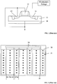
Figure 1 shows a schematic cross-section view of an existing GGNMOS protection circuit. Referring toFigure 1 , the ESD protection circuit includes asubstrate 10, a P-type well region 11 formed in thesubstrate 10, agate structure 12 formed on the surface of the P-type well region 11, an N-type source electrode 13 and an N-type drain electrode 14 formed in the P-type well region 11 on the two sides of thegate structure 12. The N-type source electrode 13, the P-type well region 11, and the N-type drain electrode 14 together form a parasitic NPN transistor. Specifically, thesource electrode 13 is the emitter of the parasitic transistor, thedrain electrode 14 is the collector of the parasitic transistor, and the P-type well region 11 is the base region of the parasitic transistor. Further, thesource electrode 13, the P-type well region 11, and the gate electrode of thegate structure 12 are grounded, and an electrostatic voltage is applied to thedrain electrode 14. - According to existing ESD device designs, because the electrostatic current may often be large, a number of transistors are usually used and connected in parallel with each other in order to improve the ESD protection ability of the device.
- However, conventional ESD protection devices may still not be able to provide sufficient ESD protection. The disclosed electrostatic discharge protection devices and fabrication methods thereof are directed to solve one or more problems set forth above and other problems in the art.
- A first aspect of the present invention provides an ESD protection device. The ESD protection device includes a substrate including a device region. The device region further includes a center region and two edge regions separated by the center region. The ESD protection device also includes an ESD protection structure formed on the substrate in the device region, and the ESD protection structure further includes a plurality of gate structures. Moreover, the ESD protection device includes a dielectric layer formed to cover the plurality of gate structures and a plurality of heat dissipation structures formed on the dielectric layer with each heat dissipation structure aligned with a corresponding gate structure along a direction perpendicular to a surface of the substrate. The area size of each heat dissipation structure aligned with a corresponding gate structure in the center region is larger than the area size of each heat dissipation structure aligned with a corresponding gate structure in the edge region.
- Preferably, the device region further includes a transition region between the center region and each edge region.
- Preferably, an area size of each heat dissipation structure aligned with a corresponding gate structure in the transition region gradually decreases along a direction from the center region to the edge region.
- Preferably, the area size of the heat dissipation structure in the center region has a largest area size under design rules.
- Preferably, the plurality of heat dissipation structures are made of metal.
- Preferably, a distance between a bottom of the heat dissipation structure and a top of the corresponding gate structure is about 150 nm or less.
- Preferably, each heat dissipation structure includes at least one heat dissipation layer configured in parallel with the surface of the substrate.
- Preferably, about one to three heat dissipation layers are included in each heat dissipation structure.
- Preferably, each heat dissipation structure includes multiple heat dissipation layers.
- Preferably, a distance between neighboring heat dissipation layers is less than 300 nm.
- Preferably, neighboring heat dissipation layers are connected with each other through a plurality of thermal conductive plugs.
- Preferably, the plurality of thermal conductive plugs are made of metal.
- Preferably, a number of thermal conductive plugs formed in each heat dissipation structure in the center region is greater than a number of thermal conductive plugs formed in each heat dissipation structure in the edge region.
- Preferably, the device region further includes: a transition region between the center region and each edge region; and a number of thermal conductive plugs formed in each heat dissipation structure above the gate structures in the transition region gradually decreases along a direction from the center region to the edge region.
- Preferably, the number of thermal conductive plugs formed in each heat dissipation structure in the center region has a greatest number under design rules.
- Preferably, each heat dissipation structure includes a plurality of equally-sized sub-structures.
- Preferably, sub-structures in each heat dissipation structure aligned with a corresponding gate structure in the center region have a density greater than sub-structures in each heat dissipation structure aligned with a corresponding gate structure in the edge region.
- Preferably, the device region further includes a transition region between the center region and each edge region.
- Preferably, a density of sub-structures in each heat dissipation structure aligned with a gate structure in the transition region gradually deceases along a direction from the center region to the edge region.
- Preferably, the plurality of sub-structures are uniformly distributed above the gate structure along a length direction of the gate structure.
- Preferably, the plurality of gate structures are arranged in parallel with each other.
- Preferably, the ESD protection device, including a gate grounded NMOS-FET device, includes: a plurality of source regions and a plurality of drain regions formed in the substrate of the device region, wherein each gate structure is situated between a source region and a drain region, and neighboring gate structures share a common source region or a common drain region; and a plurality of connection plugs each connecting to a source region or a drain region, wherein the connection plugs are arranged along a length direction of the heat dissipation structures and used as inputs or outputs for electrostatic charges.
- A second aspect of the present invention provides a method for fabricating an ESD protection device. The fabrication method includes providing a substrate including a device region and forming an ESD protection structure on the substrate in the device region. The device region further includes a center region and edge regions separated by the center region, while the ESD protection structure further includes a plurality of gate structures. The fabrication method also includes forming a dielectric layer to cover the plurality of gate structures and then forming a plurality of heat dissipation structures on the dielectric layer with each heat dissipation structure aligned with a corresponding gate structure along a direction perpendicular to a surface of the substrate. The area size of each heat dissipation structure aligned with a corresponding gate structure in the center region is larger than the area size of each heat dissipation structure aligned with a corresponding gate structure in the edge region.
- Preferably, the device region further includes an transition region between the center region and each edge region.
- Preferably, an area size of each heat dissipation structure aligned with a corresponding gate structure in the transition region gradually decreases along a direction from the center region to the edge region.
- Preferably, the heat dissipation structures are made of metal.
- An ESD protection device according to the first aspect of the present invention is obtainable by a method according to the second aspect of the present invention for fabricating an ESD protection device.
- Other aspects of the present invention can be understood by those skilled in the art in light of the description, the claims, and the drawings of the present invention.
- The following drawings are merely examples for illustrative purposes according to various disclosed embodiments and are not intended to limit the scope of the present invention as defined in the claims.
-
Figure 1 illustrates a schematic cross-section view of an existing GGNMOS protection device; -
Figure 2 illustrates a schematic top view of an existing ESD protection device; -
Figure 3 illustrates a schematic top view of an exemplary ESD protection device consistent with disclosed embodiments; -
Figure 4 illustrates a schematic cross-section view of the ESD protection device shown inFigure 3 along an AA line; -
Figure 5 illustrates schematic views of another exemplary ESD protection device consistent with disclosed embodiments; and -
Figure 6 illustrates a flowchart of the exemplary fabrication process for an ESD protection device consistent with disclosed embodiments. - Reference will now be made in detail to exemplary embodiments of the invention, which are illustrated in the accompanying drawings. Wherever possible, the same reference numbers will be used throughout the drawings to refer to the same or like parts.
- Existing ESD protection devices may not be able to provide sufficient ESD protection for semiconductor chips. This may be because the transistors may not be uniformly switched and lack of operation uniformity.
-
Figure 2 shows a schematic top view of an existing ESD protection device. For illustration purpose, the ESD protection device inFigure 2 is a GGNMOS protection device including a plurality of N-type FETs. - Referring to
Figure 2 , the ESD protection device is formed by a number of transistors that are connected in parallel with each other. Specifically, the ESD protection device includes asubstrate 20. The substrate further includes adevice region 21 and aconnection layer 24. Further, thedevice region 21 includes a plurality ofgate structures 22 and the plurality ofgate structures 22 are arranged in parallel with each other. Thedevice region 21 also includes a plurality ofsource regions 23s and a plurality ofdrain regions 23d formed on the two sides of thegate structures 22. Moreover, neighboringgate structures 22 share asource region 23s or adrain region 23d. That is, the plurality ofsource regions 23s and the plurality ofdrain regions 23d are formed alternately between neighboringgate structures 22. In addition, thegate structures 22 of the plurality of N-type FETs are grounded through theconnection layer 24 in order to form the GGNMOS protection device. - Due to the consideration of layout design, the
connection layer 24 used for grounding is often separated from thedevice region 21 in existing ESD protection devices. Therefore, the N-type transistors at different locations in thedevice region 21 may have different parasitic resistances. During the operation of the ESD protection device, heat generated from gate structures at different locations may be different and the temperature of gate structures at different locations may also be different, which may further lead to different threshold voltages for the N-type transistors at different locations. Therefore, the N-type transistors at different locations may not switch simultaneously, causing lack of operation uniformity and thus affecting the ESD ability of the ESD protection device. - The present invention provides an ESD protection device.
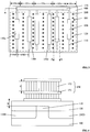
Figure 3 shows a schematic top view of an ESD protection device consistent with disclosed embodiments.Figure 4 shows a schematic cross-section view of the ESD protection device shown inFigure 3 along an AA line. For illustration purposes, the ESD protection device shown inFigure 3 includes a plurality of GGNOMS-FETs, although any other types of semiconductor components/devices may be optionally or additionally included in the disclosed ESD protection device according to various embodiments of the present invention. - Referring to
Figures 3-4 , the ESD protection device may include asubstrate 100. Thesubstrate 100 may include adevice region 101 used to form an ESD protection structure. A plurality ofgate structures 110 may be formed on the surface of thesubstrate 100 in thedevice region 101, and adielectric layer 120 may be formed to cover the plurality ofgate structures 110. - The
substrate 100 may be used to provide an operation platform for the semiconductor process. The region of thesubstrate 100 used to form the ESD protection structure may be thedevice region 101. Thesubstrate 100 may be made of single crystalline silicon, polycrystalline silicon, or amorphous silicon. Thesubstrate 100 may also be made of germanium, gallium arsenide (GaAs), or silicon germanium (SiGe). Thesubstrate 100 may have a structure with an epitaxial layer or may be silicon on an epitaxial layer. Moreover, thesubstrate 100 may also be made of any appropriate semiconductor material. In one embodiment, thesubstrate 100 is made of silicon. - The
device region 101 may be used to form an ESD protection structure. In one embodiment, the ESD protection structure formed in thedevice region 101 may be a GGNMOS protection device including a plurality of N-type FETs. Therefore, besides the plurality ofgate structures 110, thesubstrate 100 may also include a plurality ofsource regions 130S and a plurality ofdrain regions 130D. In addition, because the ESD protection structure is a GGNMOS protection structure, the doping type of the FETs in the GGNMOS protection structure is N-type. - Each
gate structure 110 together with asource region 130S and adrain region 130D may form an FET. Therefore, eachgate structure 110 may be formed between acorresponding source region 130S and acorresponding drain region 130D. Thegate structure 110 may be used to control the channel between thesource region 130S and thedrain region 130D switching from a 'switch-on' status to a 'cut-off' status, and vice versa. In addition, the plurality ofgate structures 110 may also be connected to ground to release electrostatic charge. Specifically, the gate electrode of eachgate structure 110 may be connected to the ground through aconnection layer 170. - In one embodiment, neighboring
gate structures 110 may share acommon source region 130S or acommon drain region 130D in order to improve the integration degree and reduce the size of the ESD protection device. That is, the plurality ofsource regions 130S and the plurality ofdrain regions 130D may be formed alternately in the interspace between neighboringgate structures 110. - In one embodiment, in a plane parallel to the surface of the
substrate 100 and along a direction perpendicular to the length direction of the plurality ofgate structures 110, the width of thedrain regions 130D may be larger than the width of thesource regions 130S in order to improve the operation uniformity of the ESD protection device. - Moreover, a plurality of
gate structures 110 may be formed on the surface of thesubstrate 100 in thedevice region 101. In order to improve the protection ability of the ESD protection device, the plurality ofgate structures 110 may be formed in parallel with each other. - One terminal of each
gate structure 110 in thedevice region 101 may be connected to theconnection layer 170 situated outside of thedevice region 101. Therefore, the plurality ofgate structures 110 may simultaneously release electrostatic charges through theconnection layer 170. - Further, a
dielectric layer 120 may be formed to cover the plurality ofgate structures 110. Thedielectric layer 120 covering the plurality of gate structures may be used to electrically isolate different device layers. In one embodiment, thedielectric layer 120 may be made of SiOx. - In a plane parallel to the surface of the
substrate 100 and along the direction perpendicular to the length direction of thegate structures 110, thedevice region 101 may include acenter region 101c and twoedge regions 101e separated by thecenter region 101c. However, theconnection layer 170 may extend along the direction perpendicular to the length direction of the plurality ofgate structures 110. Therefore, transistors located at different locations may correspond to different parasitic resistances. As a result, during the operation of the ESD protection device, heat generated fromgate structures 110 may be different at different locations and the temperature ofgate structures 110 may also be different at different locations. Specifically, heat generated fromgate structures 110 in thecenter region 101c may be more than heat generated fromgate structures 110 in theedge region 101e so that the temperature atgate structures 110 in thecenter region 101c may be higher than the temperature atgate structure 110 in theedge region 101e. Therefore, the variation in the temperature of thegate structures 110 at different locations may further lead to different threshold voltage for thegate structures 110 at different locations and, thus, may affect the switching uniformity of the transistors during the operation of the ESD protection device. - Further, the ESD protection device may also include a plurality of
heat dissipation structures 150 formed on thedielectric layer 120. The plurality ofheat dissipation structures 150 may be situated above the plurality ofgate structures 110. Specifically, theheat dissipation structures 150 formed above thegate structures 110 in thecenter region 101c may be firstheat dissipation structures 150c whileheat dissipation structures 150 formed above theedge regions 101e may be secondheat dissipation structures 150e. The area size of each firstheat dissipation structure 150c may be larger than the area size of each secondheat dissipation structure 150e. - When the area size of the
heat dissipation structure 150 is greater, heat generated from thegate structures 110 under theheat dissipation structure 150 may be more easily dissipated through theheat dissipation structure 150. In one embodiment, because the area size of the firstheat dissipation structure 150c is larger than the area size of the secondheat dissipation structure 150e, heat generated from thegate structures 110 under the firstheat dissipation structures 150c may be more easily dissipated than heat generated from thegate structures 110 under the secondheat dissipation structures 150e. That is, heat generated from thegate structures 110 in thecenter region 101c may be more easily dissipated than heat generated from thegate structures 110 in theedge regions 101e. As such, theheat dissipation structure 150 may be designed to have better heat dissipation ability forgate structures 110 that generate more heat. Therefore, the layout design of theheat dissipation structure 150 may help overcome the problem of having nonuniform temperature ingate structures 110 at different locations, and thus may avoid variation in the threshold voltage of the transistors due to nonuniform temperature. Therefore, the switching uniformity of the transistors during the operation of the ESD protection device may be improved. - In one embodiment, the
device region 101 may also include atransition region 101t between thecenter region 101c and eachedge region 101e. Accordingly, thegate structures 110 in the transition region 100t may be covered by a plurality of thirdheat dissipation structures 150t. The plurality of thirdheat dissipation structures 150t may be configured in parallel with the firstheat dissipation structures 150c as well as the secondheat dissipation structures 150e. - The area size of the third
heat dissipation structure 150t may be smaller than the area size of the firstheat dissipation structure 150c but larger than the area size of the secondheat dissipation structure 150e. When the number of the thirdheat dissipation structures 150t formed between thecenter region 101c and eachedge region 101e is more than one, the area sizes of the thirdheat dissipation structures 150t may gradually decrease along a direction from thecenter region 101c to thecorresponding edge region 101e. - In one embodiment, in order to improve the heat dissipation ability of the first
heat dissipation structure 150c and the performance of the ESD protection device, the area size of the firstheat dissipation structure 150c may be designed as the largest area size under the design rules. Specifically, the design rules are rules describing the capability of semiconductor process. Moreover, the design rules may appear in forms of the smallest values allowed for geometric line-width, spacing, overlapping ratio of mask layers, etc. Therefore, the largest area size under the design rules is equivalent to the largest area size allowed within the capability of semiconductor process. In one embodiment, the area size of the firstheat dissipation structure 150c may be designed as the larges area size allowed within the capability of semiconductor process. - In one embodiment, a plurality of
gate structures 110 may be formed on the surface of thesubstrate 100 in thedevice region 101 and the plurality ofgate structures 110 may be arranged in parallel with each other. Further, in one embodiment, eachheat dissipation structure 150 may have a rectangular shape. Therefore, the plurality ofheat dissipation structures 150 formed above thegate structures 110 may also be parallel with each other. Moreover, the plurality ofheat dissipation structures 150 may also be parallel with thegate structures 110. - Further, the
heat dissipation structures 150 may be made of metal. Metal is an ideal thermal conductor. Therefore, using a metal to form theheat dissipation structures 150 may effectively improve the heat dissipation rate, and thus improve the heat dissipation ability of theheat dissipation structures 150. - Referring to
Figure 4 , the distance h between theheat dissipation structures 150 and thecorresponding gate structures 110 may not be too large or too small. When the distance h between theheat dissipation structures 150 and thecorresponding gate structures 110 is too large, heat generated from thegate structures 110 may not be easily conducted to theheat dissipation structure 150 and then be dissipated from theheat dissipation structure 150. Therefore, a large distance h between theheat dissipation structures 150 and thecorresponding gate structures 110 may not be conducive to reducing the temperature of thegate structures 110. In one embodiment, the distance between the bottom of theheat dissipation structure 150 and the top of thecorresponding gate structure 110 may be less than 150 nm to provide desired heat dissipation. - Referring to
Figure 4 , theheat dissipation structure 150 may further include one of multiple heat dissipation layers 151. When the number of the heat dissipation layers 151 in eachheat dissipation structure 150 is too small, the surface area of theheat dissipation structure 150 may be too small to improve the heat dissipation ability. However, when the number of the heat dissipation layers 151 in eachheat dissipation structure 150 is too large, the structure of theheat dissipation structure 150 may become complicated, and thus the fabrication process for theheat dissipation structure 150 may be difficult. In one embodiment, the number of the heat dissipation layers 151 in eachheat dissipation structure 150 may be in a range between 1 and 3. - The
heat dissipation structure 150 may include multiple heat dissipation layers 151. Further, a small distance d between neighboring heat dissipation layers 151 may not help heat dissipation and thus may not be conducive to improving heat dissipation ability of theheat dissipation structure 150. However, a large distance d between neighboring heat dissipation layers 151 may increase the volume of theheat dissipation structure 150. In one embodiment, the distance between neighboring heat dissipation layers 151 may be smaller than 300 nm. - In one embodiment, the
heat dissipation structure 150 may include three heat dissipation layers 151. Theheat dissipation structure 150 may also include a plurality of thermalconductive plugs 152 formed between neighboring heat dissipation layers 151. The plurality of thermalconductive plugs 152 may be made of metal. Therefore, the heat transfer rate along a direction from theheat dissipation layer 151 close to thecorresponding gate structure 110 to theheat dissipation layer 151 away from thecorresponding gate structure 110 may be effectively improved, and thus the heat dissipation ability of theheat dissipation structures 150 may also be improved. - The number of thermal
conductive plugs 152 in the firstheat dissipation structure 150c may be larger than the number of thermalconductive plugs 152 in the secondheat dissipation structure 150e. Therefore, the heat transfer rate in the firstheat dissipation structure 150c may be larger than the heat transfer rate in the secondheat dissipation structure 150e. Moreover, the area size of the firstheat dissipation structure 150c may be larger than the area size of the secondheat dissipation structure 150e, theheat dissipation structure 150c may demonstrate better ability in dissipating heat generated from theunderneath gate structures 110 than theheat dissipation structure 150e. That is, heat generated fromgate structures 110 in thecenter region 101c may be easier to be dissipated than heat generated fromgate structures 110 in theedge region 101e. As such, difference in the temperatures of thegate structures 110 at different locations may be overcome and variation in the threshold voltages due to temperature differences may also be suppressed. Therefore, the switching uniformity of the transistors in the ESD protection device may be improved. - In one embodiment, the
device region 101 may also include a transition region 100t between thecenter region 101c and eachedge region 101e. Accordingly, the number of the thermal conductive plugs 152 in theheat dissipation structure 150 above thegate structures 110 may gradually decrease in thetransition region 101t along a direction from thecenter region 101c to thecorresponding edge region 101e. - In one embodiment, in order to improve the heat dissipation ability of the first
heat dissipation structure 150c and the performance of the ESD protection device, the number of the thermal conductive plugs 152 in the firstheat dissipation structure 150c may take the largest value under the design rules. As described above, the design rules are rules describing the capability of semiconductor process. Therefore, the largest number under of the thermal conductive plugs 152 according to the design rules in the firstheat dissipation structure 150c is equivalent to the largest number of the thermal conductive plugs 152 allowed in the firstheat dissipation structure 150c based on the capability of semiconductor process. - Further, in one embodiment, a plurality of connection plugs 160 may be formed in the
substrate 110 of thedevice region 101. The plurality of connection plugs 160 may be used as inputs and/or outputs for electrostatic charges. - The connection plugs 160 formed in the
substrate 100 of thedevice region 101 may be electrically connected to correspondingsource regions 130S and/ordrain regions 130D and may serve as inputs and/or outputs for electrostatic charges. In one embodiment, the ESD protection device may include a plurality of connection plugs 160. The plurality of connection plugs may be arranged along the length direction of theheat dissipation structures 150. Specifically, eachheat dissipation structure 150 may have a rectangular shape and may be arranged in parallel with thegate structures 110; accordingly, the plurality of connection plugs 160 may also be arranged along the length direction of theheat dissipation structures 150. -
Figure 5 shows a schematic top view of another exemplary ESD protection device consistent with various disclosed embodiments. Referring toFigure 5 , the ESD protection device may include a substrate (not labeled). The substrate may further include adevice region 201 and a connection layer (not labeled). A plurality ofgate structures 210 may be formed on the surface of the substrate in thedevice region 201. A dielectric layer (not labeled) may be formed to cover the plurality ofgate structures 210. A plurality of source regions (not labeled) and a plurality of drain regions (not labeled) may be alternately formed in the interspace between neighboringgate structures 210. - Compared to the ESD protection device shown in
Figures 3-4 , the ESD protection device shown inFigure 5 includes a plurality ofheat dissipation structures 250 with eachheat dissipation structure 250 further including a plurality of equally-sized sub-structures 251. Referring toFigure 5 , thesub-structures 251 formed above thegate structures 210 in thecenter region 201 c arefirst sub-structures 251 c while thesub-structures 251 formed above thegate structures 210 in theedge region 201 e arefirst sub-structures 251e. Each firstheat dissipation structure 250c may be formed by a plurality offirst sub-structures 251c and each secondheat dissipation structure 250e may be formed by a plurality ofsecond sub-structures 251e. - In one embodiment, the area size of the first
heat dissipation structure 250c may be larger than the area size of the secondheat dissipation structure 250e while the area size of eachfirst sub-structure 251 c may be equal to the area size of each second sub-structures 251e. Therefore, the number of thefirst sub-structures 251 c in each firstheat dissipation structure 250c may be larger than the number of thesecond sub-structures 251e in each secondheat dissipation structure 250e. - Moreover, in one embodiment, the
device region 201 of the ESD protection device may also include atransition region 201t between thecenter region 201 c and eachedge region 201e. Accordingly, thegate structures 210 in thetransition region 101t may be covered by a plurality of thirdheat dissipation structures 250t. Similar to the firstheat dissipation structures 250c and the second firstheat dissipation structures 250e, each thirdheat dissipation structure 250t may be formed by a plurality of equally-sized sub-structures 251. - Further, the number of
sub-structures 251 formed in each thirdheat dissipation structure 250t may be less than the number offirst sub-structures 251 c formed in each firstheat dissipation structure 250c in thecenter region 201 c, but more than the number ofsecond sub-structures 251e formed in each secondheat dissipation structure 250e in theedge region 201e. - For example, each first
heat dissipation structure 250c in thecenter region 201c may include 6first sub-structures 251 c while each secondheat dissipation structure 250e in theedge region 201 e may include 4second sub-structures 251e, the number of thesub-structures 251 to form aheat dissipation structure 250 in thetransition region 201t may be 5. - Moreover, when the number of the third
heat dissipation structures 250t formed between thecenter region 201 c and eachedge region 201e is more than one, the number of sub-structures 251t formed in the thirdheat dissipation structures 250t may decrease in thetransition region 201t along a direction from thecenter region 201 c to thecorresponding edge region 201e. - In one embodiment, the density (and/or number) of
sub-structures 251 formed on agate structure 210 in the center region may be linearly decreased with increasing the distance between thecorresponding gate structure 210 and the center of thedevice region 201 c along the direction perpendicular to the length direction of thegate structure 210. That is, the density of thesub-structures 251 may reach a highest value in thecenter region 201 c and may be linearly decreased as the position moves away from thecenter region 201 c along the direction perpendicular to the length direction of thegate structures 210. - Further, the plurality of
sub-structures 251 may be uniformly distributed over thegate structures 210 along the length direction of thegate structures 210 in order to improve the temperature uniformity of thegate structures 210. The plurality ofsub-structures 251 may be arranged in a line along the length direction of thecorresponding gate structure 210. - Referring to
Figure 5 , the number ofsub-structures 251 formed on thegate structures 210 may gradually decrease along the direction from thecenter region 201c to theedge region 201 e. Therefore, the ability to dissipate heat generated from thegate structures 210 may also gradually decrease along the direction from thecenter region 201c to theedge region 201e. As such, difference in the temperatures of thegate structures 210 at different locations may be overcome and variation in the threshold voltages due to temperature differences may also be suppressed. Therefore, the switching uniformity of the transistors in the ESD protection device may be improved. - The present invention also provides a method for fabricating an ESD protection device.
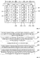
Figure 6 shows a flowchart of the fabrication process for the ESD protection device consistent with disclosed embodiments.Figure 3 shows a schematic top-view of the ESD protection device andFigure 4 shows a cross-section view of the structure shown inFigure 3 along an AA line. - Referring to
Figure 6 , at the beginning of the fabrication process, a substrate including a connection layer and a device region may be provided and the device region of the substrate may further include a center region and two edge regions separated by the center region (S601). Referring toFigure 3 , asubstrate 100 including adevice region 101 and aconnection layer 170 may be provided. In one embodiment, thedevice region 101 of thesubstrate 100 may include acenter region 101c and twoedge regions 101e separated by thecenter region 101c. In other embodiment, thedevice region 101 may further include atransition region 101t between thecenter region 101c and eachedge region 101e. - Referring to
Figure 6 , a plurality of gate structures, a plurality of source regions, and a plurality of drain regions may be formed in the device region (S602). Referring toFigure 3 , a plurality ofgate structures 110, a plurality ofsource regions 130S, and a plurality ofdrain regions 130D may be formed in thedevice region 101. Specifically, neighboringgate structures 110 may share acommon source region 130S or acommon drain region 130D. Therefore, the plurality ofsource regions 130S and the plurality ofdrain regions 130D may be alternately formed in the interspace between neighboringgate structures 110. In one embodiment, thegate structures 110 may be formed in both thecenter region 101c and the twoedge regions 101e. In other embodiment, thedevice region 101 may also include atransition region 101t between thecenter region 101c and eachedge region 101e; accordingly, thegate structures 110 may also be formed in thetransition region 101t. - The plurality of
gate structures 110, a plurality ofsource regions 130S, and a plurality ofdrain regions 130D may be formed in parallel with each other. That is, the length directions of thegate structures 110, thesource regions 130S, and thedrain regions 130D are all along one direction. - Further, returning to
Figure 6 , a dielectric layer may be formed to cover the device region (S603). Referring toFigure 4 , thedielectric layer 120 may cover the plurality ofgate structures 110, the plurality ofsource regions 130S, and the plurality ofdrain regions 130D. - In a subsequent process, a heat dissipation structure may be formed on the
dielectric layer 120 above eachgate structure 110. Therefore, the thickness of thedielectric layer 120 formed on eachgate structure 110 may not be too large; otherwise, heat generated from thegate structures 110 may not be easily conducted to the heat dissipation structure. In one embodiment, the thickness of thedielectric layer 120 formed on eachgate structure 110 may be less than 150 nm. - Returning to
Figure 6 , further, a plurality of connection plugs may be formed in the substrate of the device region to electrically connect to the source regions and the drain regions (S604). - Referring to
Figure 3 , a plurality of connection plugs 160 may be formed in thesubstrate 110 of thedevice region 101. Eachconnection plug 160 may be electrically connected to acorresponding source region 130S or adrain region 130D and serve as an input or an output for electrostatic charges. The plurality of connection plugs may be arranged along the length direction of thegate structures 110. - Further, returning to
Figure 6 , a plurality of heat dissipation structures may be formed on the dielectric layer above the gate structures with the area size of the heat dissipation structure formed above each gate structure in the center region greater than the area size of the heat dissipation structure formed above each gate structure in the edge region (S605). - Referring to
Figure 3 , a plurality ofheat dissipation structures 150 may be formed on thedielectric layer 120 over thegate structures 110. Specifically, theheat dissipation structures 150 formed above thegate structures 110 in thecenter region 101c may be firstheat dissipation structures 150c whileheat dissipation structures 150 formed above theedge regions 101e may be secondheat dissipation structures 150e. The area size of each firstheat dissipation structure 150c may be larger than the area size of each secondheat dissipation structure 150e. - When the area size of the
heat dissipation structure 150 is bigger, heat generated from thegate structures 110 under theheat dissipation structure 150 may be more easily dissipated through theheat dissipation structure 150. In one embodiment, because the area size of the firstheat dissipation structure 150 c is larger than the area size of the secondheat dissipation structure 150e, heat generated from thegate structures 110 under the firstheat dissipation structures 150c may be more easily dissipated than heat generated from thegate structures 110 under the secondheat dissipation structures 150e. That is, heat generated from thegate structures 110 in thecenter region 101c may be more easily dissipated than heat generated from thegate structures 110 in theedge regions 101e. As such, theheat dissipation structure 150 may be arranged to have better heat dissipation ability forgate structures 110 that generate more heat. Therefore, the layout design of theheat dissipation structure 150 may help overcome the problem of having nonuniform temperature ingate structures 110 at different locations, and thus may avoid variation in the threshold voltage of the transistors due to nonuniform temperature. Therefore, the switching uniformity of the transistors during the operation of the ESD protection device may be improved. - In one embodiment, the
device region 101 may also include a transition region 100t between thecenter region 101c and eachedge region 101e. Accordingly, a plurality of thirdheat dissipation structures 150t may be formed over thegate structures 110 in thetransition region 101t. The plurality of thirdheat dissipation structures 150t may be parallel to the firstheat dissipation structures 150c as well as the secondheat dissipation structures 150e. - The area size of the third
heat dissipation structure 150t may be smaller than the area size of the firstheat dissipation structure 150c but larger than the area size of the secondheat dissipation structure 150e. When the number of the thirdheat dissipation structures 150t formed between thecenter region 101c and eachedge region 101e is more than one, the area sizes of the thirdheat dissipation structures 150t may gradually decrease along a direction from thecenter region 101c to thecorresponding edge region 101e. - In one embodiment, in order to improve the heat dissipation ability of the first
heat dissipation structure 150c and the performance of the ESD protection device, the area size of the firstheat dissipation structure 150c may be designed as the largest area size under the design rules. Specifically, the design rules are rules describing the capability of semiconductor process. Moreover, the design rules may appear in forms of the smallest values allowed for geometric line-width, spacing, overlapping ratio of mask layers, etc. Therefore, the largest area size under the design rules is equivalent to the largest area size allowed within the capability of semiconductor process. In one embodiment, the area size of the firstheat dissipation structure 150c may be designed as the larges area size allowed within the capability of semiconductor process. - In one embodiment, a plurality of
gate structures 110 may be formed on the surface of thedevice region 101 in thesubstrate 100 and the plurality ofgate structures 110 may be arranged in parallel with each other. Further, eachheat dissipation structure 150 may have a rectangular shape. Therefore, the plurality ofheat dissipation structures 150 formed above thegate structures 110 may also be parallel to each other and theheat dissipation structures 150 may also be parallel to thegate structures 110. - Moreover, the
heat dissipation structures 150 may be made of metal. Metal is an ideal thermal conductor. Therefore, using a metal to form theheat dissipation structures 150 may effectively improve the heat dissipation rate, and thus improve the heat dissipation ability of theheat dissipation structures 150. - Referring to
Figure 4 , theheat dissipation structure 150 may further include one of multiple heat dissipation layers 151. When the number of the heat dissipation layers 151 in eachheat dissipation structure 150 is too small, the surface area of theheat dissipation structure 150 may be too small to improve the heat dissipation ability. However, when the number of the heat dissipation layers 151 in eachheat dissipation structure 150 is too large, the structure of theheat dissipation structure 150 may become complicated, and thus the fabrication process for theheat dissipation structure 150 may be difficult. In one embodiment, the number of the heat dissipation layers 151 in eachheat dissipation structures 150 may be in a range of 1 to 3. - The
heat dissipation structure 150 may include multiple heat dissipation layers 151. Further, a small distance d between neighboring heat dissipation layers 151 may not help heat dissipation and thus may not be conducive to improving heat dissipation ability of theheat dissipation structure 150. However, a large distance d between neighboring heat dissipation layers 151 may increase the volume of theheat dissipation structure 150. In one embodiment, the distance between neighboring heat dissipation layers 151 may be smaller than 300 nm. - In one embodiment, the
heat dissipation structure 150 may include three heat dissipation layers 151. Theheat dissipation structure 150 may also include a plurality of thermalconductive plugs 152 formed between neighboring heat dissipation layers 151. The plurality of thermalconductive plugs 152 may be made of metal. Therefore, the heat transfer rate along a direction from theheat dissipation layer 151 close to thecorresponding gate structure 110 to theheat dissipation layer 151 away from thecorresponding gate structure 110 may be effectively improved, and thus the heat dissipation ability of theheat dissipation structures 150 may also be improved. - The number of thermal
conductive plugs 152 in the firstheat dissipation structure 150c may be larger than the number of thermalconductive plugs 152 in the secondheat dissipation structure 150e. Therefore, the heat transfer rate in the firstheat dissipation structure 150c may be larger than the heat transfer rate in the secondheat dissipation structure 150e. Moreover, the area size of the firstheat dissipation structure 150c may be larger than the area size of the secondheat dissipation structure 150e, theheat dissipation structure 150c may demonstrate better ability in dissipating heat generated from theunderneath gate structures 110 than theheat dissipation structure 150e. That is, heat generated fromgate structures 110 in thecenter region 101c may be easier to be dissipated than heat generated fromgate structures 110 in theedge region 101e. As such, difference in the temperatures of thegate structures 110 at different locations may be overcome and variation in the threshold voltages due to temperature differences may also be suppressed. Therefore, the switching uniformity of the transistors in the ESD protection device may be improved. - In one embodiment, the
device region 101 may also include a transition region 100t between thecenter region 101c and eachedge region 101e. Accordingly, the number of the thermal conductive plugs 152 in theheat dissipation structure 150 above thegate structures 110 may gradually decrease in thetransition region 101t along a direction from thecenter region 101c to thecorresponding edge region 101e. - In one embodiment, in order to improve the heat dissipation ability of the first
heat dissipation structure 150c and the performance of the ESD protection device, the number of the thermal conductive plugs 152 in the firstheat dissipation structure 150c may take the largest value under the design rules. As described above, the design rules are rules describing the capability of semiconductor process. Therefore, the largest number under of the thermal conductive plugs 152 the design rules in the firstheat dissipation structure 150c is equivalent to the largest number of the thermal conductive plugs 152 allowed in the firstheat dissipation structure 150c based on the capability of semiconductor process. - In another embodiment, referring to
Figure 5 , eachheat dissipation structure 250 formed on the dielectric layer above acorresponding gate structure 210 may include a plurality of equally-sized sub-structures 251. Thesub-structures 251 formed above thegate structures 210 in thecenter region 201 c arefirst sub-structures 251 c while thesub-structures 251 formed above thegate structures 210 in theedge region 201e arefirst sub-structures 251e. Each firstheat dissipation structure 250c may be formed by a plurality offirst sub-structures 251 c and each secondheat dissipation structure 250e may be formed by a plurality ofsecond sub-structures 251e. - The area size of the first
heat dissipation structure 250c may be larger than the area size of the secondheat dissipation structure 250e while the area size of eachfirst sub-structure 251c may be equal to the area size of each second sub-structures 251e. Therefore, the number of thefirst sub-structures 251 c in each firstheat dissipation structure 250c may be larger than the number of thesecond sub-structures 251e in each secondheat dissipation structure 250e. - Moreover, the
device region 201 of the ESD protection device may also include atransition region 201t between thecenter region 201 c and eachedge region 201e. Accordingly, thegate structures 210 in thetransition region 101t may be covered by a plurality of thirdheat dissipation structures 250t. Similar to the firstheat dissipation structures 250c and the second firstheat dissipation structures 250e, each thirdheat dissipation structure 250t may be formed by a plurality of equally-sized sub-structures 251. - Further, the number of
sub-structures 251 formed in each thirdheat dissipation structure 250t may be less than the number offirst sub-structures 251 c formed in each firstheat dissipation structure 250c in thecenter region 201 c, but more than the number ofsecond sub-structures 251e formed in each secondheat dissipation structure 250e in theedge region 201 e. - For example, each first
heat dissipation structure 250c in thecenter region 201c may include 6first sub-structures 251 c while each secondheat dissipation structure 250e in theedge region 201e may include 4second sub-structures 251e, the number of thesub-structures 251 to form aheat dissipation structure 250 in thetransition region 201t may be 5. - Moreover, when the number of the third
heat dissipation structures 250t formed between thecenter region 201 c and eachedge region 201 e is more than one, the number of sub-structures 251t formed in the thirdheat dissipation structures 250t may decrease in thetransition region 201t along a direction from thecenter region 201c to thecorresponding edge region 201e. - In addition, the density (and/or number) of
sub-structures 251 formed on agate structure 210 in the center region may be linearly decreased with increasing the distance between thecorresponding gate structure 210 and the center of thedevice region 201 c along the direction perpendicular to the length direction of thegate structure 210. That is, the density of thesub-structures 251 may reach a highest value in thecenter region 201 c and may be linearly decreased as the position moves away from thecenter region 201 c along the direction perpendicular to the length direction of thegate structures 210. - Further, the plurality of
sub-structures 251 may be uniformly distributed over thegate structures 210 along the length direction of thegate structures 210 in order to improve the temperature uniformity of thegate structures 210. The plurality ofsub-structures 251 may be arranged in a line along the length direction of thecorresponding gate structure 210. - Referring to
Figure 5 , the number ofsub-structures 251 formed on thegate structures 210 may gradually decrease along the direction from thecenter region 201c to theedge region 201 e. Therefore, the ability to dissipate heat generated from thegate structures 210 may also gradually decrease along the direction from thecenter region 201c to theedge region 201e. As such, difference in the temperatures of thegate structures 210 at different locations may be overcome and variation in the threshold voltages due to temperature differences may also be suppressed. Therefore, the switching uniformity of the transistors in the ESD protection device may be improved. - Compared to existing ESD protection devices, the disclosed ESD protection device may demonstrate advantages in improving the operation uniformity of the device.
- Specifically, the disclosed ESD protection device may include a substrate including a device region used to form the ESD protection structure. The disclosed ESD protection device may further include a plurality of gate structures formed on the surface of the substrate in the device region and a dielectric layer formed to cover the plurality of gate structures. In a plane parallel to the surface of the substrate, the device region may further include a center region and two edge regions separated by the center region along a direction perpendicular to the length direction of the gate structures. The disclosed ESD may also include a plurality of heat dissipation structures formed on the surface of the dielectric layer in the device region. Each heat dissipation structure may be formed above a corresponding gate structure. Each heat dissipation structure formed on a gate structure in the center region is a first heat dissipation structure, while each heat dissipation structure formed on a gate structure in the edge region is a second heat dissipation structure. The area size of the first heat dissipation structure may be larger than the area size of the second dissipation structure.
- According to the disclosed ESD protection device, by forming the plurality of heat dissipation structures on the surface of the dielectric layer above the gate structures, the ability of the ESD protection device to dissipate heat generated from the gate structures may be improved. Moreover, according to the disclosed ESD protection device, the heat dissipation structures formed over the gate structures in the center region of the device may be first heat dissipation structures while the heat dissipation structures formed over the gate structures in the edge region of the device may be second heat dissipation structures. Further, because the area size of the first heat dissipation structures may be larger than the area size of the second heat dissipation structures, heat generated from the gate structures in the center region may be more easily dissipated than heat generated from the gate structures in the edge regions. As such, the layout design of the heat dissipation structure in the ESD protection device may help overcome the problem of having nonuniform temperature in gate structures at different locations, and thus may improve the temperature uniformity for gate structures at different locations and also improve the uniformity in the threshold voltages of the transistors at different locations. Therefore, the switching uniformity of the transistors may be improved, and thus the performance of the formed ESD protection device may also be improved.
Claims (15)
- An electrostatic discharge, ESD, protection device, comprising:a substrate including a device region, the device region including a center region and edge regions separated by the center region;an ESD protection structure including a plurality of gate structures, formed on the substrate in the device region;a dielectric layer formed to cover the plurality of gate structures;a plurality of heat dissipation structures formed on the dielectric layer and each aligned with a corresponding gate structure along a direction perpendicular to a surface of the substrate, wherein:an area size of each heat dissipation structure aligned with a corresponding gate structure in the center region is larger than an area size of each heat dissipation structure aligned with a corresponding gate structure in the edge region.
- The ESD protection device according to claim 1, wherein:the device region further includes a transition region between the center region and each edge region; andthe area size of each heat dissipation structure aligned with a corresponding gate structure in the transition region gradually decreases along a direction from the center region to the edge region.
- The ESD protection device according to claim 1 or 2, wherein the ESD protection device is characterized by at least one of:the area size of the heat dissipation structure in the center region has a largest area size under design rules;the plurality of heat dissipation structures are made of metal; anda distance between a bottom of the heat dissipation structure and a top of the corresponding gate structure is about 150 nm or less.
- The ESD protection device according to any one of the claims 1-3, wherein each heat dissipation structure includes at least one heat dissipation layer configured in parallel with the surface of the substrate.
- The ESD protection device according to claim 4, wherein about one to three heat dissipation layers are included in each heat dissipation structure.
- The ESD protection device according to claim 4, wherein:each heat dissipation structure includes multiple heat dissipation layers;a distance between neighboring heat dissipation layers is less than 300 nm; andneighboring heat dissipation layers are connected with each other through a plurality of thermal conductive plugs, wherein preferably: the plurality of thermal conductive plugs are made of metal.
- The ESD protection device according to claim 6, wherein:a number of thermal conductive plugs formed in each heat dissipation structure in the center region is greater than a number of thermal conductive plugs formed in each heat dissipation structure in the edge region.
- The ESD protection device according to claim 7, wherein:the device region further includes a transition region between the center region and each edge region; anda number of thermal conductive plugs formed in each heat dissipation structure above the gate structures in the transition region gradually decreases along a direction from the center region to the edge region, wherein preferably: the number of thermal conductive plugs formed in each heat dissipation structure in the center region has a greatest number under design rules.
- The ESD protection device according to any one of the claims 1-8, wherein:each heat dissipation structure includes a plurality of equally-sized sub-structures; andsub-structures in each heat dissipation structure aligned with a corresponding gate structure in the center region have a density greater than sub-structures in each heat dissipation structure aligned with a corresponding gate structure in the edge region.
- The ESD protection device according to claim 9, wherein:the device region further includes a transition region between the center region and each edge region; and a density of sub-structures in each heat dissipation structure aligned with a gate structure in the transition region gradually deceases along a direction from the center region to the edge region; and/orthe plurality of sub-structures are uniformly distributed above the gate structure along a length direction of the gate structure.
- The ESD protection device according to any one of the claims 1-10, wherein:the plurality of gate structures are arranged in parallel with each other.
- The ESD protection device according to any one of the claims 1-11, including a gate grounded NMOS-FET device, including:a plurality of source regions and a plurality of drain regions formed in the substrate of the device region, wherein each gate structure is situated between a source region and a drain region, and neighboring gate structures share a common source region or a common drain region; anda plurality of connection plugs each connecting to a source region or a drain region, wherein the connection plugs are arranged along a length direction of the heat dissipation structures and used as inputs or outputs for electrostatic charges.
- A method for forming an ESD protection device, comprising:providing a substrate including a device region, the device region including a center region and edge regions separated by the center region;forming an ESD protection structure, including a plurality of gate structures, on the substrate in the device region;forming a dielectric layer to cover the plurality of gate structures; andforming a plurality of heat dissipation structures on the dielectric layer and each aligned with a corresponding gate structure along a direction perpendicular to a surface of the substrate, wherein:an area size of each heat dissipation structure aligned with a corresponding gate structure in the center region is larger than an area size of each heat dissipation structure aligned with a corresponding gate structure in the edge region.
- The method for forming the ESD protection device according to claim 13, wherein:the device region further includes an transition region between the center region and each edge region; andan area size of each heat dissipation structure aligned with a corresponding gate structure in the transition region gradually decreases along a direction from the center region to the edge region.
- The method for forming the ESD protection device according to claim 13 or 14, wherein the heat dissipation structures are made of metal.
Applications Claiming Priority (1)
| Application Number | Priority Date | Filing Date | Title |
|---|---|---|---|
| CN201610083826.8A CN107046028A (en) | 2016-02-05 | 2016-02-05 | Electrostatic discharge protector |
Publications (1)
| Publication Number | Publication Date |
|---|---|
| EP3203516A1 true EP3203516A1 (en) | 2017-08-09 |
Family
ID=57909493
Family Applications (1)
| Application Number | Title | Priority Date | Filing Date |
|---|---|---|---|
| EP17153216.1A Withdrawn EP3203516A1 (en) | 2016-02-05 | 2017-01-26 | Electrostatic discharge protection device and fabrication method thereof |
Country Status (3)
| Country | Link |
|---|---|
| US (1) | US10535583B2 (en) |
| EP (1) | EP3203516A1 (en) |
| CN (1) | CN107046028A (en) |
Families Citing this family (1)
| Publication number | Priority date | Publication date | Assignee | Title |
|---|---|---|---|---|
| CN109427762B (en) * | 2017-08-22 | 2020-12-18 | 中芯国际集成电路制造(上海)有限公司 | Electrostatic Discharge Transistor Array Device |
Citations (4)
| Publication number | Priority date | Publication date | Assignee | Title |
|---|---|---|---|---|
| US6316827B1 (en) * | 1997-09-12 | 2001-11-13 | Nec Corporation | Semiconductor device having improved temperature distribution |
| US6407445B1 (en) * | 2000-10-06 | 2002-06-18 | National Semiconductor Corporation | MOSFET-based electrostatic discharge (ESD) protection structure with a floating heat sink |
| US20060284261A1 (en) * | 2005-06-21 | 2006-12-21 | Saptharishi Sriram | Semiconductor devices having varying electrode widths to provide non-uniform gate pitches and related methods |
| US20150311191A1 (en) * | 2014-04-24 | 2015-10-29 | Infineon Technologies Dresden Gmbh | Semiconductor device comprising electrostatic discharge protection structure |
Family Cites Families (4)
| Publication number | Priority date | Publication date | Assignee | Title |
|---|---|---|---|---|
| US6455898B1 (en) * | 1999-03-15 | 2002-09-24 | Macronix International Co., Ltd. | Electrostatic discharge input protection for reducing input resistance |
| US20070022847A1 (en) * | 2005-07-28 | 2007-02-01 | Terence Chen | Positioning device for positioning driving member in wrench |
| JP4519097B2 (en) * | 2006-03-29 | 2010-08-04 | ルネサスエレクトロニクス株式会社 | Semiconductor device |
| DE102016115822B4 (en) * | 2016-08-25 | 2025-06-26 | Infineon Technologies Dresden GmbH & Co. KG | SEMICONDUCTOR DEVICE HAVING A STRUCTURE FOR PROTECTING AGAINST ELECTROSTATIC DISCHARGE |
-
2016
- 2016-02-05 CN CN201610083826.8A patent/CN107046028A/en active Pending
-
2017
- 2017-01-17 US US15/407,290 patent/US10535583B2/en active Active
- 2017-01-26 EP EP17153216.1A patent/EP3203516A1/en not_active Withdrawn
Patent Citations (4)
| Publication number | Priority date | Publication date | Assignee | Title |
|---|---|---|---|---|
| US6316827B1 (en) * | 1997-09-12 | 2001-11-13 | Nec Corporation | Semiconductor device having improved temperature distribution |
| US6407445B1 (en) * | 2000-10-06 | 2002-06-18 | National Semiconductor Corporation | MOSFET-based electrostatic discharge (ESD) protection structure with a floating heat sink |
| US20060284261A1 (en) * | 2005-06-21 | 2006-12-21 | Saptharishi Sriram | Semiconductor devices having varying electrode widths to provide non-uniform gate pitches and related methods |
| US20150311191A1 (en) * | 2014-04-24 | 2015-10-29 | Infineon Technologies Dresden Gmbh | Semiconductor device comprising electrostatic discharge protection structure |
Also Published As
| Publication number | Publication date |
|---|---|
| US20170229369A1 (en) | 2017-08-10 |
| CN107046028A (en) | 2017-08-15 |
| US10535583B2 (en) | 2020-01-14 |
Similar Documents
| Publication | Publication Date | Title |
|---|---|---|
| US8748278B2 (en) | Method for fabricating semiconductor device | |
| KR101352685B1 (en) | Vertical Butt and Scr for ESD | |
| CN102903716B (en) | The output buffer of combination and ESD diode device | |
| US10186507B2 (en) | Electrostatic discharge protection structure and fabricating method thereof | |
| US20120319164A1 (en) | Semiconductor device | |
| KR20130119439A (en) | Vertical semiconductor device with thinned substrate | |
| US12002890B2 (en) | Semiconductor protection device | |
| JP4844621B2 (en) | Transistor-type protection device and semiconductor integrated circuit | |
| EP3154086B1 (en) | Electrostatic discharge protection device and method for forming the same | |
| EP3001457B1 (en) | Lil enhanced esd-pnp in a bcd | |
| TWI784064B (en) | Gate-controlled bipolar junction transistor and operation method thereof | |
| US9627210B2 (en) | Method of fabricating electrostatic discharge protection structure | |
| CN104299966B (en) | Electrostatic discharge protection structure | |
| CN107046029A (en) | ESD-protection structure and forming method thereof | |
| US10535583B2 (en) | Electrostatic discharge protection device and fabrication method thereof | |
| CN114068696B (en) | Semiconductor device including a plurality of trenches | |
| TWI703702B (en) | Field effect transistor and semiconductor device | |
| CN114171513B (en) | Electrostatic discharge protection structure and method for forming the same | |
| TW202315040A (en) | A device for electrostatic discharge protection | |
| TWI566376B (en) | Semiconductor device and method of manufacturing same | |
| US11011510B2 (en) | Breakdown uniformity for ESD protection device | |
| US20260006869A1 (en) | Backside substrate dielectric break | |
| TWI763029B (en) | Vertical bipolar transistor device | |
| JP5494519B2 (en) | Transistor-type protection device and semiconductor integrated circuit | |
| CN114171514B (en) | Electrostatic discharge protection structure and forming method thereof |
Legal Events
| Date | Code | Title | Description |
|---|---|---|---|
| PUAI | Public reference made under article 153(3) epc to a published international application that has entered the european phase |
Free format text: ORIGINAL CODE: 0009012 |
|
| STAA | Information on the status of an ep patent application or granted ep patent |
Free format text: STATUS: THE APPLICATION HAS BEEN PUBLISHED |
|
| AK | Designated contracting states |
Kind code of ref document: A1 Designated state(s): AL AT BE BG CH CY CZ DE DK EE ES FI FR GB GR HR HU IE IS IT LI LT LU LV MC MK MT NL NO PL PT RO RS SE SI SK SM TR |
|
| AX | Request for extension of the european patent |
Extension state: BA ME |
|
| STAA | Information on the status of an ep patent application or granted ep patent |
Free format text: STATUS: REQUEST FOR EXAMINATION WAS MADE |
|
| 17P | Request for examination filed |
Effective date: 20171120 |
|
| RBV | Designated contracting states (corrected) |
Designated state(s): AL AT BE BG CH CY CZ DE DK EE ES FI FR GB GR HR HU IE IS IT LI LT LU LV MC MK MT NL NO PL PT RO RS SE SI SK SM TR |
|
| STAA | Information on the status of an ep patent application or granted ep patent |
Free format text: STATUS: EXAMINATION IS IN PROGRESS |
|
| 17Q | First examination report despatched |
Effective date: 20180925 |
|
| RAP1 | Party data changed (applicant data changed or rights of an application transferred) |
Owner name: SEMICONDUCTOR MANUFACTURING INTERNATIONAL (SHANGHA Owner name: SEMICONDUCTOR MANUFACTURING INTERNATIONAL (BEIJING |
|
| STAA | Information on the status of an ep patent application or granted ep patent |
Free format text: STATUS: THE APPLICATION IS DEEMED TO BE WITHDRAWN |
|
| 18D | Application deemed to be withdrawn |
Effective date: 20191108 |