EP3202038B1 - Komparator - Google Patents
Komparator Download PDFInfo
- Publication number
- EP3202038B1 EP3202038B1 EP15782021.8A EP15782021A EP3202038B1 EP 3202038 B1 EP3202038 B1 EP 3202038B1 EP 15782021 A EP15782021 A EP 15782021A EP 3202038 B1 EP3202038 B1 EP 3202038B1
- Authority
- EP
- European Patent Office
- Prior art keywords
- comparator
- voltage
- supply
- terminal
- stage
- Prior art date
- Legal status (The legal status is an assumption and is not a legal conclusion. Google has not performed a legal analysis and makes no representation as to the accuracy of the status listed.)
- Active
Links
Images


Classifications
-
- H—ELECTRICITY
- H03—ELECTRONIC CIRCUITRY
- H03K—PULSE TECHNIQUE
- H03K5/00—Manipulating of pulses not covered by one of the other main groups of this subclass
- H03K5/22—Circuits having more than one input and one output for comparing pulses or pulse trains with each other according to input signal characteristics, e.g. slope, integral
- H03K5/24—Circuits having more than one input and one output for comparing pulses or pulse trains with each other according to input signal characteristics, e.g. slope, integral the characteristic being amplitude
- H03K5/2472—Circuits having more than one input and one output for comparing pulses or pulse trains with each other according to input signal characteristics, e.g. slope, integral the characteristic being amplitude using field effect transistors
- H03K5/2481—Circuits having more than one input and one output for comparing pulses or pulse trains with each other according to input signal characteristics, e.g. slope, integral the characteristic being amplitude using field effect transistors with at least one differential stage
-
- H—ELECTRICITY
- H03—ELECTRONIC CIRCUITRY
- H03K—PULSE TECHNIQUE
- H03K19/00—Logic circuits, i.e. having at least two inputs acting on one output; Inverting circuits
- H03K19/02—Logic circuits, i.e. having at least two inputs acting on one output; Inverting circuits using specified components
- H03K19/08—Logic circuits, i.e. having at least two inputs acting on one output; Inverting circuits using specified components using semiconductor devices
- H03K19/094—Logic circuits, i.e. having at least two inputs acting on one output; Inverting circuits using specified components using semiconductor devices using field-effect transistors
- H03K19/09432—Logic circuits, i.e. having at least two inputs acting on one output; Inverting circuits using specified components using semiconductor devices using field-effect transistors with coupled sources or source coupled logic
-
- H—ELECTRICITY
- H03—ELECTRONIC CIRCUITRY
- H03K—PULSE TECHNIQUE
- H03K5/00—Manipulating of pulses not covered by one of the other main groups of this subclass
- H03K5/22—Circuits having more than one input and one output for comparing pulses or pulse trains with each other according to input signal characteristics, e.g. slope, integral
- H03K5/24—Circuits having more than one input and one output for comparing pulses or pulse trains with each other according to input signal characteristics, e.g. slope, integral the characteristic being amplitude
- H03K5/2472—Circuits having more than one input and one output for comparing pulses or pulse trains with each other according to input signal characteristics, e.g. slope, integral the characteristic being amplitude using field effect transistors
- H03K5/249—Circuits having more than one input and one output for comparing pulses or pulse trains with each other according to input signal characteristics, e.g. slope, integral the characteristic being amplitude using field effect transistors using clock signals
Definitions
- This invention relates to a comparator, which may also be described as a comparator circuit, stage, or module, and to apparatus comprising a comparator.
- Comparators are well-known electronic circuits, for incorporation in a wide variety of circuits and apparatus.
- Fig:1 shows a generic symbol representation of a comparator, where VCC is the positive power supply, VDD is the negative power supply, or can be ground, e+ is the input positive sense (voltage range is normally VDD + X to VCC - Y), and e- is the input negative sense (voltage range is normally VDD + X to VCC - Y).
- the OUTPUT signal When the voltage applied to e+ is higher than the voltage applied to e-, the OUTPUT signal is a logic 1 (close to VCC).
- the OUTPUT signal is a logic 0 (close to VDD).
- the simple basic accuracy Input offset voltage
- Input offset voltage is typically a few mV to a few tens of mV.
- the current comparator implementations typically use differential, mirror current for the front stage, followed by an amplification stage. This requires close to identical transistors, in most cases using complementary transistors as well. Their accuracy (or precision) is mostly linked to the variation between transistors, and even a very small variation has an amplified error effect. Thus, problems associated with known comparators are the need to use closely matched transistors, and the errors associated with use of transistors not closely matched.
- US5798658A discloses source-coupled logic with reference controlled inputs.
- US4410815A discloses a high speed gallium arsenide (GaAs) integrated circuit which converts GaAs input or source signals to voltage levels for directly driving emitter coupled logic (ECL) circuits.
- GaAs gallium arsenide
- US4237388A discloses an inverter circuit operating at a high speed and with low power consumption, which comprises a first bipolar transistor having a collector coupled to the output of the circuit, a second bipolar transistor having a collector coupled to the base of the first transistor and means responsive to at least one input signal to produce a first signal for driving the first transistor and a second signal complementary to the first signal for driving the second transistor substantially at the same time.
- One aspect of the present invention provides a comparator for comparing a first input voltage with a second input voltage and generating a corresponding output voltage, the comparator comprising: a first input terminal for receiving the first input voltage: a second input terminal for receiving the second input voltage; an output terminal for outputting the output voltage; a first supply rail for providing a first supply voltage; and a second supply rail for providing a second supply voltage, the comparator further comprising: a follower stage comprising a first follower stage supply terminal coupled to the first supply rail, a second follower stage supply terminal coupled to the second supply rail, a follower stage input terminal coupled to the second input terminal, and a follower stage output terminal for providing a follower stage output voltage; an inverter stage comprising a first inverter stage supply terminal coupled to the first supply rail, a second inverter stage supply terminal coupled to the follower stage output terminal, an inverter stage input terminal coupled to the first input terminal, and an inverter stage output terminal for providing an inverter stage output voltage and coupled to the
- the comparator output voltage may switch (alternate) between two states in close and accurate correspondence with the first input voltage exceeding the second voltage and vice versa.
- the comparator output may accurately reflect the relationship (comparison) between the two input voltages.
- the follower stage comprises tuning means for adjusting the follower stage output voltage as a function of voltage provided to the follower stage input terminal.
- this can enable the offset voltages of the two stages to be made very similar, thereby improving accuracy of the comparator output.
- the follower stage tuning means comprises a resistor, which may be a variable resistor.
- the inverter stage comprises tuning means for adjusting the inverter stage output voltage as a function of voltage provided to the inverter stage input terminal.
- this tuning means may comprise a resistor, which may be fixed or variable.
- Certain embodiments further comprise signal conditioning means (e.g. a signal conditioning stage, circuit, or module) coupled between the inverter stage output terminal and the comparator output terminal.
- This signal conditioning means may convert the inverter output signal (which may be regarded as a "half-digital" signal, to a signal having a wider range (e.g. to a "full-digital” signal, such as a signal alternating between two supply voltages).
- the inverter stage output voltage has a first range, in use, determined by the voltage applied to the first supply rail and by the follower stage output voltage, and the signal conditioning means is adapted to generate, from the inverter stage output voltage, a comparator output voltage at the comparator output terminal having a second range, where the second range is larger than the first range.
- the second range extends substantially from a voltage supplied to the first supply rail to a voltage supplied to the second supply rail.
- the first supply voltage is a positive supply voltage.
- said second supply rail is connected to ground (in other words, said second supply rail may be a ground rail).
- the comparator further comprises a voltage converter (e.g. a DC to DC converter) coupled to the first and second supply rails and to the second follower stage supply terminal and arranged to generate a negative supply voltage and supply said negative supply voltage to the second follower stage supply terminal.
- a voltage converter e.g. a DC to DC converter
- the second supply voltage is a negative supply voltage.
- the follower stage comprises a transistor.
- this transistor is an enhancement mode field effect transistor, FET.
- this FET has a gate terminal coupled to the follower stage input terminal, a drain terminal coupled to the first follower stage supply terminal, and a source terminal coupled to the follower stage output terminal and to the second follower stage supply terminal.
- the source terminal is coupled to the second follower stage supply terminal by a resistor.
- the inverter stage comprises a transistor.
- this inverter stage transistor is an enhancement mode field effect transistor, FET, but in alternative embodiments different mode FETs may be used (e.g. depletion mode FETs).
- the inverter stage FET has a gate terminal coupled to the inverter stage input terminal, a drain terminal coupled to the first inverter stage supply terminal and to the inverter stage output terminal, and a source terminal coupled to the follower stage output terminal.
- the inverter stage FET drain terminal is coupled to the first inverter stage supply terminal by a resistor.
- the filtering means may, for example, be a band pass filter.
- the filtering means may be arranged to filter a range, or band, of frequencies from the output voltage.
- the filtering means is arranged to filter out a band of frequencies, including the fundamental frequency.
- Another aspect of the invention provides apparatus including a comparator in accordance with any of the above-mentioned aspects or embodiments.
- the apparatus is an operational amplifier.
- the comparator approach uses N type transistors only, and relies on offsetting the threshold voltages, Vth, of the two input transistors.(linked to e+ and e-). The closer the Vth of those two transistors, the higher the comparator accuracy is. The accuracy is also achieved by keeping the linearity under control over the input range. For a better linearity, a positive and negative voltage can be applied.
- the comparator may utilise different transistors, i.e. transistors, such as P type transistors, other than N type transistors.
- the comparator may comprise transistors of more than one type, for example it may utilise both N and P type transistors.
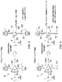
- Fig 2 is a block diagram of a comparator useful for understanding the invention.
- the comparator 100 is for comparing a first input voltage e+ with a second input voltage e- and generating a corresponding output voltage.
- the comparator 100 comprises: a first input terminal 1 for receiving the first input voltage: a second input terminal 2 for receiving the second input voltage; an output terminal 3 for outputting the output voltage; a first supply rail 4 for providing a first supply voltage (VCC); and a second supply rail 5 for providing a second supply voltage.
- VCC first supply voltage
- the comparator further comprises: a follower stage 6 comprising a first follower stage supply terminal 61 coupled to the first supply rail 4, a second follower stage supply terminal 62 coupled to the second supply rail 5, a follower stage input terminal 63 coupled to the second input terminal 2, and a follower stage output terminal 64 for providing a follower stage output voltage; and an inverter stage 7 comprising a first inverter stage supply terminal 71 coupled to the first supply rail 4, a second inverter stage supply terminal 72 coupled to the follower stage output terminal 64, an inverter stage input terminal 73 coupled to the first input terminal 1, and an inverter stage output terminal 74 for providing an inverter stage output voltage and coupled to the output terminal 3.
- the first input terminal 1 is directly connected to the inverter input terminal 73 and is provided with first input voltage (or signal) (e+)
- the second input terminal 2 is directly connected to the follower stage input terminal 63 and is provided with second input signal or voltage (e-).
- A indicated as 6 in the figure, is a follower stage with its output (e-Ref) equal to (e-) minus the follower stage transistor threshold voltage (Vth_e-).
- B is an inverter stage with its reference (i.e. the low supply voltage) being (e-Ref), so its output (e+lnverter) will be triggered when (e+) is higher than (e-Ref) plus its own (Vth_e+).
- B's output signal (e+lnverter), is only a "half digital signal", where its high level is close to VCC, but its low level is proportional to e- input, so a signal conditioning and conversion from "half digital signal” to digital is required in certain embodiments.
- This signal conditioning and conversion to a full digital signal (e.g. alternating between two supply rail voltages) is provided by the signal conditioning module 8 illustrated in fig. 2 , coupled between the inverter output terminal 74 and the comparator output terminal 3.
- Figs. 3 and 4 illustrate example implementations of follower and inverter stages A and B, where tuning the transistors geometry with respective matching of tuning resistors Re- and Re+, labelled 90 and 91 respectively, allows us to increase the comparator accuracy.
- the values of the two resistors may be tuned, selected, adjusted, or otherwise arranged to compensate for differences between the threshold voltages of the two enhancement mode FETS 10, 11, such that the resultant comparator output accurately switches in response to e+ exceeding e-, and vice versa. This provides a straightforward way of constructing a highly accurate comparator, without requiring very close matching of transistor properties.
- Tuning resistor 90 in fig. 3 is connected between the source of the FET 10 (which is connected to output terminal 64) and the second supply terminal 62 (which is connected to the second supply rail 5). In certain embodiments, resistor 90 has a fixed value. In other embodiments, resistor 90 is a variable resistor. Tuning resistor 91 in fig.
- resistor 91 has a fixed value. In other embodiments, resistor 91 is a variable resistor.
- B's output signal (e+lnverter), is only a "half digital signal", where its high level is close to VCC, but its low level is proportional to e- input, So a signal conditioning and conversion from "half digital signal” to digital is required.
- a follower stage 81 is used in the signal conditioning stage 810, which may also be described as a signal conditioner, or signal conditioning circuit or module, to adapt the impedance to impact as little as possible the comparator front stages.
- an analog to digital converter 82 which may also be described as an A/D stage or A/D means
- an inverter 83 to have the correct OUTPUT signal phase.
- the conversion from "half digital signal” into digital signal may be implemented using traditional sums of subtractions and voltage divisions, the details of which will be apparent to the skilled person and so are not set out in this specification.
- Fig 6, 7 and 8 illustrate several possible implementations in different examples useful for understanding the invention.
- the DC/DC converter has inputs 51, 52 connected to ground (the second supply rail 5 in this example) and to the first supply rail 4 respectively, and generates supply voltage VDD at an output terminal 53 which is connected to the second follower supply terminal 62.
- the second follower supply terminal 62 is thus coupled to the second supply rail via the voltage converter 50, which is itself connected to ground and to the first supply rail.
- Fig 7 illustrates a comparator providing the same accuracy/linearity as the comparator of fig. 6 , but requires provision of an external negative voltage, as this example comprises no internal DC to DC converter able to generate a negative voltage from a positive voltage and ground.
- the comparator of fig. 8 is supplied with only GND and VCC, and does not incorporate a DC to DC converter for generating a negative supply voltage, so exhibits lower accuracy than those of figs. 6 and 7 due to decreased linearity.
- the comparator of fig. 8 may provide the advantages of greater simplicity/reduced complexity, and reduced cost.
- the second supply rail is a ground rail.
- this shows another comparator embodying the invention.
- This comparator has similar structure to that of the embodiment shown in fig. 2 , but also incorporates some additional features, as follows.
- this embodiment has two additional parts, labelled C (an oscillator and switching device) and D (a pass band, or band pass, filter).
- C an oscillator and switching device
- D a pass band, or band pass, filter.
- the goal of this embodiment is to avoid potential “Bias Stress” effects, from transistors to comparator. Those potential “Bias Stress” effects are only seen at DC and low frequencies (typically sub 10Hz). Potential “Bias Stress” effects, have a detrimental effect on comparator functionality and accuracy.
- the present embodiment incorporates a controllable switching device 300, connected between the first follower supply terminal 61 and the first supply rail 4, such that the state of the switching device determines whether the supply voltage VCC is being supplied to the first follower supply terminal or not.
- the switch 300 (which may take a variety of forms, as will be apparent to the skilled person, is controllable to turn the voltage supply to the first follower supply terminal on an off (such that the voltage at that terminal alternates between VCC and zero volts, for example).
- the comparator 100 further comprises control means for controlling the switch 300, in this embodiment in the form an oscillator 30, connected to the positive supply rail 4 and to ground GND.
- the oscillator is arranged to provide a control signal 301 to the switch to control the switch's state.
- the control signal is a substantially a square wave
- the switching device 300 is responsive to the control signal 301 to alternate (i.e. switch) between a closed state, in which it connects the supply rail 4 to follower terminal 61, and an open state, it which it disconnects the supply rail from follower terminal 61.
- the oscillator may have a minimum frequency of a few tens of Hz. By incorporating the oscillator in this manner and switching the device 300 on and off, this has the effect of switching ON/OFF the follower output (e- Ref) of the follower A, 6.
- the pass band filter 20 is added at the output of the comparator (in fact, in this example, just before the comparator output terminal 3).
- the filter 20 is thus connected between the inverter output 74 and the comparator output 3.
- the embodiment of fig. 9 comprises module 8, connected between terminals 74 and 3, in series with the filter 20, but may be omitted in certain alternative embodiments.
- the band pass filter allows the comparator to get rid of the "unwanted" frequency component, introduced by the oscillator 30 controlling the switching device 300, from the output signal provided to terminal 3.
- to filter is arranged to eliminate frequency components (from the comparator output) corresponding to the switching frequency of the switching device 300.
Landscapes
- Physics & Mathematics (AREA)
- Nonlinear Science (AREA)
- Engineering & Computer Science (AREA)
- Power Engineering (AREA)
- Computer Hardware Design (AREA)
- Computing Systems (AREA)
- General Engineering & Computer Science (AREA)
- Mathematical Physics (AREA)
- Analogue/Digital Conversion (AREA)
- Manipulation Of Pulses (AREA)
Claims (15)
- Komparator (100) zum Vergleichen einer ersten Eingangsspannung mit einer zweiten Eingangsspannung und zum Erzeugen einer entsprechenden Ausgangsspannung, wobei der Komparator umfasst:einen ersten Eingangsanschluss (1) zum Empfangen der ersten Eingangsspannung;einen zweiten Eingangsanschluss (2) zum Empfangen der zweiten Eingangsspannung;einen Ausgangsanschluss (3) zum Ausgeben der Ausgangsspannung;eine erste Versorgungsschiene (4) zum Bereitstellen einer ersten Versorgungsspannung; undeine zweite Versorgungsschiene (5) zum Bereitstellen einer zweiten Versorgungsspannung,wobei der Komparator ferner umfasst:eine Folgerstufe (6), umfassend einen ersten Folgerstufen-Versorgungsanschluss (61), der an die erste Versorgungsschiene gekoppelt ist, einen zweiten Folgerstufen-Versorgungsanschluss (62), der an die zweite Versorgungsschiene gekoppelt ist, einen Folgerstufen-Eingangsanschluss (63), der an den zweiten Eingangsanschluss gekoppelt ist, und einen Folgerstufen-Ausgangsanschluss (64) zum Bereitstellen einer Folgerstufen-Ausgangsspannung;eine Inverterstufe (7), umfassend einen ersten Inverterstufen-Versorgungsanschluss (71), der an die erste Versorgungsschiene gekoppelt ist, einen zweiten Inverterstufen-Versorgungsanschluss (72), der an den Folgerstufen-Ausgangsanschluss gekoppelt ist, einen Inverterstufen-Eingangsanschluss (73), der an den ersten Eingangsanschluss gekoppelt ist, und einen Inverterstufen-Ausgangsanschluss (74) zum Bereitstellen einer Inverterstufen-Ausgangsspannung, der an den Ausgangsanschluss gekoppelt ist;dadurch gekennzeichnet, dass der Komparator ferner umfasst:eine steuerbare Schaltvorrichtung (300), die dazu angeordnet ist, den ersten Folgerstufen-Versorgungsanschluss (61) an die erste Versorgungsschiene (4) zu koppeln, wobei die Schaltvorrichtung dazu steuerbar ist, zwischen einem ersten Zustand, in dem sie den ersten Folgerstufen-Versorgungsanschluss mit der ersten Versorgungsschiene verbindet, und einem zweiten Zustand, in dem sie den ersten Folgerstufen-Versorgungsanschluss von der ersten Versorgungsschiene elektrisch trennt, zu wechseln;ein Steuermittel, das dazu angeordnet ist, die steuerbare Schaltvorrichtung zu steuern; undein Filtermittel (20), das zwischen dem Inverterstufen-Ausgangsanschluss (74) und dem Komparator-Ausgangsanschluss (3) angeordnet ist, um mindestens eine Frequenzkomponente aus der Ausgangsspannung zu filtern,wobei das Steuermittel einen Oszillator (30) umfasst, der einen Ausgang aufweist, der dazu angeordnet ist, die Schaltvorrichtung (300) so zu steuern, dass sie zwischen dem ersten und dem zweiten Zustand wechselt, der Oszillatorausgang eine Grundfrequenz aufweist und das Filtermittel (20) dazu angeordnet ist, mindestens die Grundfrequenz herauszufiltern.
- Komparator nach Anspruch 1, wobei die Folgerstufe (6) Abstimmmittel zum Einstellen der Folgerstufen-Ausgangsspannung als Funktion der dem Folgerstufen-Eingangsanschluss bereitgestellten Spannung umfasst.
- Komparator nach Anspruch 2, wobei das Folgerstufen-Abstimmmittel einen Widerstand (90) umfasst.
- Komparator nach einem der vorhergehenden Ansprüche, wobei die Inverterstufe (7) Abstimmmittel zum Einstellen der Inverterstufen-Ausgangsspannung als Funktion der dem Inverterstufen-Eingangsanschluss bereitgestellten Spannung umfasst.
- Komparator nach Anspruch 4, wobei das Inverterstufen-Abstimmmittel einen Widerstand (91) umfasst.
- Komparator nach einem der vorhergehenden Ansprüche, ferner umfassend ein Signalkonditionierungsmittel (8), das zwischen dem Inverterstufen-Ausgangsanschluss und dem Komparator-Ausgangsanschluss gekoppelt ist.
- Komparator nach Anspruch 6, wobei die Inverterstufen-Ausgangsspannung in Verwendung einen ersten Bereich aufweist, der durch die an die erste Versorgungsschiene angelegte Spannung und durch die Folgerstufen-Ausgangsspannung bestimmt wird, und das Signalkonditionierungsmittel dazu angepasst ist, aus der Inverterstufen-Ausgangsspannung eine Komparator-Ausgangsspannung an dem Komparator-Ausgangsanschluss zu erzeugen, die einen zweiten Bereich aufweist, wobei der zweite Bereich größer als der erste Bereich ist.
- Komparator nach Anspruch 7, wobei sich der zweite Bereich im Wesentlichen von einer der ersten Versorgungsschiene zugeführten Spannung zu einer der zweiten Versorgungsschiene zugeführten Spannung erstreckt.
- Komparator nach einem der vorhergehenden Ansprüche, wobei die erste Versorgungsspannung eine positive Versorgungsspannung ist.
- Komparator nach einem der vorhergehenden Ansprüche, wobei die zweite Versorgungsschiene mit Masse verbunden ist.
- Komparator nach Anspruch 10, ferner umfassend einen Spannungswandler (50), der mit der ersten und der zweiten Versorgungsschiene und dem zweiten Folgerstufen-Versorgungsanschluss gekoppelt und dazu angeordnet ist, eine negative Versorgungsspannung zu erzeugen und die negative Versorgungsspannung dem zweiten Folgerstufen-Versorgungsanschluss zuzuführen.
- Komparator nach einem der Ansprüche 1 bis 9, wobei die zweite Versorgungsspannung eine negative Versorgungsspannung ist.
- Komparator nach einem der vorhergehenden Ansprüche, wobei die Folgerstufe (6) einen Transistor (10) umfasst.
- Komparator nach einem der vorhergehenden Ansprüche, wobei die Inverterstufe (7) einen Transistor (11) umfasst.
- Vorrichtung, die einen Komparator nach einem der vorhergehenden Ansprüche beinhaltet.
Applications Claiming Priority (2)
| Application Number | Priority Date | Filing Date | Title |
|---|---|---|---|
| GB1417379.3A GB2530775A (en) | 2014-10-01 | 2014-10-01 | Comparator |
| PCT/GB2015/052883 WO2016051192A1 (en) | 2014-10-01 | 2015-10-01 | Comparator |
Publications (2)
| Publication Number | Publication Date |
|---|---|
| EP3202038A1 EP3202038A1 (de) | 2017-08-09 |
| EP3202038B1 true EP3202038B1 (de) | 2020-09-16 |
Family
ID=51901473
Family Applications (1)
| Application Number | Title | Priority Date | Filing Date |
|---|---|---|---|
| EP15782021.8A Active EP3202038B1 (de) | 2014-10-01 | 2015-10-01 | Komparator |
Country Status (4)
| Country | Link |
|---|---|
| US (2) | US20170302258A1 (de) |
| EP (1) | EP3202038B1 (de) |
| GB (1) | GB2530775A (de) |
| WO (1) | WO2016051192A1 (de) |
Families Citing this family (2)
| Publication number | Priority date | Publication date | Assignee | Title |
|---|---|---|---|---|
| PL3849715T3 (pl) | 2018-09-11 | 2024-02-05 | Valka Ehf | System i aparat do przetwarzania i sortowania artykułów spożywczych oraz powiązany sposób |
| US10734985B2 (en) | 2018-12-17 | 2020-08-04 | Qualcomm Incorporated | Comparators for power and high-speed applications |
Family Cites Families (12)
| Publication number | Priority date | Publication date | Assignee | Title |
|---|---|---|---|---|
| JPS4942346B1 (de) * | 1970-07-31 | 1974-11-14 | ||
| JPS544560A (en) * | 1977-06-14 | 1979-01-13 | Nec Corp | Semiconductor inverter circuit |
| US4410815A (en) * | 1981-09-24 | 1983-10-18 | Sperry Corporation | Gallium arsenide to emitter coupled logic level converter |
| US4464631A (en) * | 1981-12-01 | 1984-08-07 | Harris Corporation | Circuit for trimming FET differential pair offset voltage without increasing the offset voltage temperature coefficient |
| US5798658A (en) * | 1995-06-15 | 1998-08-25 | Werking; Paul M. | Source-coupled logic with reference controlled inputs |
| WO1998054727A2 (en) * | 1997-05-30 | 1998-12-03 | Micron Technology, Inc. | 256 Meg DYNAMIC RANDOM ACCESS MEMORY |
| US6757327B1 (en) * | 2000-10-02 | 2004-06-29 | Lsi Logic Corporation | Serial data communication receiver having adaptive termination resistors |
| JP4047178B2 (ja) * | 2003-01-06 | 2008-02-13 | 富士通株式会社 | 入力回路 |
| KR100846387B1 (ko) * | 2006-05-31 | 2008-07-15 | 주식회사 하이닉스반도체 | 반도체 메모리 소자의 온도 정보 출력 장치 |
| TWI405415B (zh) * | 2009-11-09 | 2013-08-11 | Ind Tech Res Inst | 具有背景式誤差修正功能的動態比較器 |
| JP5684081B2 (ja) * | 2011-09-22 | 2015-03-11 | 株式会社東芝 | アナログ/デジタル変換器 |
| US8604838B2 (en) * | 2011-12-12 | 2013-12-10 | Texas Instruments Incorporated | Comparator with improved time constant |
-
2014
- 2014-10-01 GB GB1417379.3A patent/GB2530775A/en not_active Withdrawn
-
2015
- 2015-10-01 US US15/515,623 patent/US20170302258A1/en not_active Abandoned
- 2015-10-01 WO PCT/GB2015/052883 patent/WO2016051192A1/en not_active Ceased
- 2015-10-01 EP EP15782021.8A patent/EP3202038B1/de active Active
-
2019
- 2019-03-05 US US16/292,961 patent/US10812059B2/en active Active
Non-Patent Citations (1)
| Title |
|---|
| None * |
Also Published As
| Publication number | Publication date |
|---|---|
| US20190199337A1 (en) | 2019-06-27 |
| US20170302258A1 (en) | 2017-10-19 |
| WO2016051192A1 (en) | 2016-04-07 |
| EP3202038A1 (de) | 2017-08-09 |
| US10812059B2 (en) | 2020-10-20 |
| GB201417379D0 (en) | 2014-11-12 |
| GB2530775A (en) | 2016-04-06 |
Similar Documents
| Publication | Publication Date | Title |
|---|---|---|
| US7595676B2 (en) | Comparator and method with controllable threshold and hysteresis | |
| US7154294B2 (en) | Comparators capable of output offset calibration | |
| CN109213248B (zh) | 负电源控制电路以及电源装置 | |
| US9602089B2 (en) | Amplifying device and offset voltage correction method | |
| CN110943702B (zh) | 用于高阻抗缓冲器的交流联接斩波器信号 | |
| US7915921B1 (en) | Circuits and methods for level shifting a signal | |
| KR20060056419A (ko) | Am 중간 주파 가변 이득 증폭 회로, 가변 이득 증폭 회로및 그 반도체 집적 회로 | |
| US8558581B2 (en) | Analog rail-to-rail comparator with hysteresis | |
| US8736310B2 (en) | Comparator with offset compensation and improved dynamic range | |
| EP3202038B1 (de) | Komparator | |
| US8471601B2 (en) | Single-ended to differential converter | |
| US7463087B2 (en) | Operational amplifier with zero offset | |
| CN117674793A (zh) | 输出电阻可编程mosfet半桥栅驱动电路 | |
| US7009442B2 (en) | Linear multiplier circuit | |
| US10784828B2 (en) | Methods and apparatus for an operational amplifier with a variable gain-bandwidth product | |
| JP2012114610A (ja) | 電子回路 | |
| Sessa et al. | Robust GaN two-stage operational transconductance amplifier using dynamic voltage shifter | |
| US7567628B2 (en) | Symmetric differential slicer | |
| CN101154930A (zh) | 自动增益控制电路 | |
| US20260118404A1 (en) | Methods and apparatus to identify a state change of a switch | |
| CN112350676A (zh) | 半导体放大电路以及半导体电路 | |
| CN111030613A (zh) | 射频信号处理电路和射频前端单元 | |
| US7236030B2 (en) | Method to implement hysteresis in a MOSFET differential pair input stage | |
| US7285998B2 (en) | Duty ratio adjusting circuit | |
| US7622964B2 (en) | Analog buffer circuit |
Legal Events
| Date | Code | Title | Description |
|---|---|---|---|
| STAA | Information on the status of an ep patent application or granted ep patent |
Free format text: STATUS: THE INTERNATIONAL PUBLICATION HAS BEEN MADE |
|
| PUAI | Public reference made under article 153(3) epc to a published international application that has entered the european phase |
Free format text: ORIGINAL CODE: 0009012 |
|
| STAA | Information on the status of an ep patent application or granted ep patent |
Free format text: STATUS: REQUEST FOR EXAMINATION WAS MADE |
|
| 17P | Request for examination filed |
Effective date: 20170427 |
|
| AK | Designated contracting states |
Kind code of ref document: A1 Designated state(s): AL AT BE BG CH CY CZ DE DK EE ES FI FR GB GR HR HU IE IS IT LI LT LU LV MC MK MT NL NO PL PT RO RS SE SI SK SM TR |
|
| AX | Request for extension of the european patent |
Extension state: BA ME |
|
| DAV | Request for validation of the european patent (deleted) | ||
| DAX | Request for extension of the european patent (deleted) | ||
| STAA | Information on the status of an ep patent application or granted ep patent |
Free format text: STATUS: EXAMINATION IS IN PROGRESS |
|
| 17Q | First examination report despatched |
Effective date: 20181126 |
|
| GRAP | Despatch of communication of intention to grant a patent |
Free format text: ORIGINAL CODE: EPIDOSNIGR1 |
|
| STAA | Information on the status of an ep patent application or granted ep patent |
Free format text: STATUS: GRANT OF PATENT IS INTENDED |
|
| INTG | Intention to grant announced |
Effective date: 20200327 |
|
| GRAS | Grant fee paid |
Free format text: ORIGINAL CODE: EPIDOSNIGR3 |
|
| GRAA | (expected) grant |
Free format text: ORIGINAL CODE: 0009210 |
|
| STAA | Information on the status of an ep patent application or granted ep patent |
Free format text: STATUS: THE PATENT HAS BEEN GRANTED |
|
| AK | Designated contracting states |
Kind code of ref document: B1 Designated state(s): AL AT BE BG CH CY CZ DE DK EE ES FI FR GB GR HR HU IE IS IT LI LT LU LV MC MK MT NL NO PL PT RO RS SE SI SK SM TR |
|
| REG | Reference to a national code |
Ref country code: GB Ref legal event code: FG4D |
|
| REG | Reference to a national code |
Ref country code: CH Ref legal event code: EP |
|
| REG | Reference to a national code |
Ref country code: DE Ref legal event code: R096 Ref document number: 602015059205 Country of ref document: DE |
|
| REG | Reference to a national code |
Ref country code: IE Ref legal event code: FG4D |
|
| REG | Reference to a national code |
Ref country code: AT Ref legal event code: REF Ref document number: 1315071 Country of ref document: AT Kind code of ref document: T Effective date: 20201015 |
|
| PG25 | Lapsed in a contracting state [announced via postgrant information from national office to epo] |
Ref country code: GR Free format text: LAPSE BECAUSE OF FAILURE TO SUBMIT A TRANSLATION OF THE DESCRIPTION OR TO PAY THE FEE WITHIN THE PRESCRIBED TIME-LIMIT Effective date: 20201217 Ref country code: NO Free format text: LAPSE BECAUSE OF FAILURE TO SUBMIT A TRANSLATION OF THE DESCRIPTION OR TO PAY THE FEE WITHIN THE PRESCRIBED TIME-LIMIT Effective date: 20201216 Ref country code: BG Free format text: LAPSE BECAUSE OF FAILURE TO SUBMIT A TRANSLATION OF THE DESCRIPTION OR TO PAY THE FEE WITHIN THE PRESCRIBED TIME-LIMIT Effective date: 20201216 Ref country code: FI Free format text: LAPSE BECAUSE OF FAILURE TO SUBMIT A TRANSLATION OF THE DESCRIPTION OR TO PAY THE FEE WITHIN THE PRESCRIBED TIME-LIMIT Effective date: 20200916 Ref country code: HR Free format text: LAPSE BECAUSE OF FAILURE TO SUBMIT A TRANSLATION OF THE DESCRIPTION OR TO PAY THE FEE WITHIN THE PRESCRIBED TIME-LIMIT Effective date: 20200916 Ref country code: SE Free format text: LAPSE BECAUSE OF FAILURE TO SUBMIT A TRANSLATION OF THE DESCRIPTION OR TO PAY THE FEE WITHIN THE PRESCRIBED TIME-LIMIT Effective date: 20200916 |
|
| REG | Reference to a national code |
Ref country code: AT Ref legal event code: MK05 Ref document number: 1315071 Country of ref document: AT Kind code of ref document: T Effective date: 20200916 |
|
| REG | Reference to a national code |
Ref country code: NL Ref legal event code: MP Effective date: 20200916 |
|
| PG25 | Lapsed in a contracting state [announced via postgrant information from national office to epo] |
Ref country code: LV Free format text: LAPSE BECAUSE OF FAILURE TO SUBMIT A TRANSLATION OF THE DESCRIPTION OR TO PAY THE FEE WITHIN THE PRESCRIBED TIME-LIMIT Effective date: 20200916 Ref country code: RS Free format text: LAPSE BECAUSE OF FAILURE TO SUBMIT A TRANSLATION OF THE DESCRIPTION OR TO PAY THE FEE WITHIN THE PRESCRIBED TIME-LIMIT Effective date: 20200916 |
|
| REG | Reference to a national code |
Ref country code: LT Ref legal event code: MG4D |
|
| PG25 | Lapsed in a contracting state [announced via postgrant information from national office to epo] |
Ref country code: LT Free format text: LAPSE BECAUSE OF FAILURE TO SUBMIT A TRANSLATION OF THE DESCRIPTION OR TO PAY THE FEE WITHIN THE PRESCRIBED TIME-LIMIT Effective date: 20200916 Ref country code: EE Free format text: LAPSE BECAUSE OF FAILURE TO SUBMIT A TRANSLATION OF THE DESCRIPTION OR TO PAY THE FEE WITHIN THE PRESCRIBED TIME-LIMIT Effective date: 20200916 Ref country code: SM Free format text: LAPSE BECAUSE OF FAILURE TO SUBMIT A TRANSLATION OF THE DESCRIPTION OR TO PAY THE FEE WITHIN THE PRESCRIBED TIME-LIMIT Effective date: 20200916 Ref country code: PT Free format text: LAPSE BECAUSE OF FAILURE TO SUBMIT A TRANSLATION OF THE DESCRIPTION OR TO PAY THE FEE WITHIN THE PRESCRIBED TIME-LIMIT Effective date: 20210118 Ref country code: RO Free format text: LAPSE BECAUSE OF FAILURE TO SUBMIT A TRANSLATION OF THE DESCRIPTION OR TO PAY THE FEE WITHIN THE PRESCRIBED TIME-LIMIT Effective date: 20200916 Ref country code: CZ Free format text: LAPSE BECAUSE OF FAILURE TO SUBMIT A TRANSLATION OF THE DESCRIPTION OR TO PAY THE FEE WITHIN THE PRESCRIBED TIME-LIMIT Effective date: 20200916 |
|
| PG25 | Lapsed in a contracting state [announced via postgrant information from national office to epo] |
Ref country code: IS Free format text: LAPSE BECAUSE OF FAILURE TO SUBMIT A TRANSLATION OF THE DESCRIPTION OR TO PAY THE FEE WITHIN THE PRESCRIBED TIME-LIMIT Effective date: 20210116 Ref country code: PL Free format text: LAPSE BECAUSE OF FAILURE TO SUBMIT A TRANSLATION OF THE DESCRIPTION OR TO PAY THE FEE WITHIN THE PRESCRIBED TIME-LIMIT Effective date: 20200916 Ref country code: AL Free format text: LAPSE BECAUSE OF FAILURE TO SUBMIT A TRANSLATION OF THE DESCRIPTION OR TO PAY THE FEE WITHIN THE PRESCRIBED TIME-LIMIT Effective date: 20200916 Ref country code: AT Free format text: LAPSE BECAUSE OF FAILURE TO SUBMIT A TRANSLATION OF THE DESCRIPTION OR TO PAY THE FEE WITHIN THE PRESCRIBED TIME-LIMIT Effective date: 20200916 Ref country code: ES Free format text: LAPSE BECAUSE OF FAILURE TO SUBMIT A TRANSLATION OF THE DESCRIPTION OR TO PAY THE FEE WITHIN THE PRESCRIBED TIME-LIMIT Effective date: 20200916 |
|
| REG | Reference to a national code |
Ref country code: CH Ref legal event code: PL |
|
| REG | Reference to a national code |
Ref country code: DE Ref legal event code: R097 Ref document number: 602015059205 Country of ref document: DE |
|
| PG25 | Lapsed in a contracting state [announced via postgrant information from national office to epo] |
Ref country code: MC Free format text: LAPSE BECAUSE OF FAILURE TO SUBMIT A TRANSLATION OF THE DESCRIPTION OR TO PAY THE FEE WITHIN THE PRESCRIBED TIME-LIMIT Effective date: 20200916 Ref country code: LU Free format text: LAPSE BECAUSE OF NON-PAYMENT OF DUE FEES Effective date: 20201001 Ref country code: SK Free format text: LAPSE BECAUSE OF FAILURE TO SUBMIT A TRANSLATION OF THE DESCRIPTION OR TO PAY THE FEE WITHIN THE PRESCRIBED TIME-LIMIT Effective date: 20200916 |
|
| REG | Reference to a national code |
Ref country code: BE Ref legal event code: MM Effective date: 20201031 |
|
| PLBE | No opposition filed within time limit |
Free format text: ORIGINAL CODE: 0009261 |
|
| STAA | Information on the status of an ep patent application or granted ep patent |
Free format text: STATUS: NO OPPOSITION FILED WITHIN TIME LIMIT |
|
| 26N | No opposition filed |
Effective date: 20210617 |
|
| PG25 | Lapsed in a contracting state [announced via postgrant information from national office to epo] |
Ref country code: SI Free format text: LAPSE BECAUSE OF FAILURE TO SUBMIT A TRANSLATION OF THE DESCRIPTION OR TO PAY THE FEE WITHIN THE PRESCRIBED TIME-LIMIT Effective date: 20200916 Ref country code: LI Free format text: LAPSE BECAUSE OF NON-PAYMENT OF DUE FEES Effective date: 20201031 Ref country code: DK Free format text: LAPSE BECAUSE OF FAILURE TO SUBMIT A TRANSLATION OF THE DESCRIPTION OR TO PAY THE FEE WITHIN THE PRESCRIBED TIME-LIMIT Effective date: 20200916 Ref country code: CH Free format text: LAPSE BECAUSE OF NON-PAYMENT OF DUE FEES Effective date: 20201031 Ref country code: BE Free format text: LAPSE BECAUSE OF NON-PAYMENT OF DUE FEES Effective date: 20201031 |
|
| PG25 | Lapsed in a contracting state [announced via postgrant information from national office to epo] |
Ref country code: IT Free format text: LAPSE BECAUSE OF FAILURE TO SUBMIT A TRANSLATION OF THE DESCRIPTION OR TO PAY THE FEE WITHIN THE PRESCRIBED TIME-LIMIT Effective date: 20200916 Ref country code: IE Free format text: LAPSE BECAUSE OF NON-PAYMENT OF DUE FEES Effective date: 20201001 |
|
| PG25 | Lapsed in a contracting state [announced via postgrant information from national office to epo] |
Ref country code: TR Free format text: LAPSE BECAUSE OF FAILURE TO SUBMIT A TRANSLATION OF THE DESCRIPTION OR TO PAY THE FEE WITHIN THE PRESCRIBED TIME-LIMIT Effective date: 20200916 Ref country code: MT Free format text: LAPSE BECAUSE OF FAILURE TO SUBMIT A TRANSLATION OF THE DESCRIPTION OR TO PAY THE FEE WITHIN THE PRESCRIBED TIME-LIMIT Effective date: 20200916 Ref country code: CY Free format text: LAPSE BECAUSE OF FAILURE TO SUBMIT A TRANSLATION OF THE DESCRIPTION OR TO PAY THE FEE WITHIN THE PRESCRIBED TIME-LIMIT Effective date: 20200916 |
|
| PG25 | Lapsed in a contracting state [announced via postgrant information from national office to epo] |
Ref country code: MK Free format text: LAPSE BECAUSE OF FAILURE TO SUBMIT A TRANSLATION OF THE DESCRIPTION OR TO PAY THE FEE WITHIN THE PRESCRIBED TIME-LIMIT Effective date: 20200916 |
|
| P01 | Opt-out of the competence of the unified patent court (upc) registered |
Effective date: 20230517 |
|
| PG25 | Lapsed in a contracting state [announced via postgrant information from national office to epo] |
Ref country code: NL Free format text: LAPSE BECAUSE OF NON-PAYMENT OF DUE FEES Effective date: 20200923 |
|
| REG | Reference to a national code |
Ref country code: DE Ref legal event code: R081 Ref document number: 602015059205 Country of ref document: DE Owner name: PRAGMATIC SEMICONDUCTOR LIMITED, GB Free format text: FORMER OWNER: PRAGMATIC PRINTING LTD, SEDGEFIELD, DURHAM, GB |
|
| PGFP | Annual fee paid to national office [announced via postgrant information from national office to epo] |
Ref country code: DE Payment date: 20241009 Year of fee payment: 10 |
|
| PGFP | Annual fee paid to national office [announced via postgrant information from national office to epo] |
Ref country code: FR Payment date: 20241009 Year of fee payment: 10 |
|
| PGFP | Annual fee paid to national office [announced via postgrant information from national office to epo] |
Ref country code: GB Payment date: 20250820 Year of fee payment: 11 |