EP3201955B1 - Silicon integrated mirror-like thermoelectric generator of out-of-plane heat flux configuration - Google Patents
Silicon integrated mirror-like thermoelectric generator of out-of-plane heat flux configuration Download PDFInfo
- Publication number
- EP3201955B1 EP3201955B1 EP15781434.4A EP15781434A EP3201955B1 EP 3201955 B1 EP3201955 B1 EP 3201955B1 EP 15781434 A EP15781434 A EP 15781434A EP 3201955 B1 EP3201955 B1 EP 3201955B1
- Authority
- EP
- European Patent Office
- Prior art keywords
- doped
- mirror
- dice
- hill
- thermoelectric generator
- Prior art date
- Legal status (The legal status is an assumption and is not a legal conclusion. Google has not performed a legal analysis and makes no representation as to the accuracy of the status listed.)
- Not-in-force
Links
- XUIMIQQOPSSXEZ-UHFFFAOYSA-N Silicon Chemical compound [Si] XUIMIQQOPSSXEZ-UHFFFAOYSA-N 0.000 title claims description 29
- 229910052710 silicon Inorganic materials 0.000 title claims description 29
- 239000010703 silicon Substances 0.000 title claims description 29
- 230000004907 flux Effects 0.000 title claims description 9
- 239000002184 metal Substances 0.000 claims description 50
- 229910052751 metal Inorganic materials 0.000 claims description 50
- 239000004065 semiconductor Substances 0.000 claims description 38
- 239000000463 material Substances 0.000 claims description 31
- 239000010409 thin film Substances 0.000 claims description 21
- 235000012431 wafers Nutrition 0.000 claims description 18
- VYPSYNLAJGMNEJ-UHFFFAOYSA-N Silicium dioxide Chemical compound O=[Si]=O VYPSYNLAJGMNEJ-UHFFFAOYSA-N 0.000 claims description 14
- 229910052581 Si3N4 Inorganic materials 0.000 claims description 5
- HQVNEWCFYHHQES-UHFFFAOYSA-N silicon nitride Chemical group N12[Si]34N5[Si]62N3[Si]51N64 HQVNEWCFYHHQES-UHFFFAOYSA-N 0.000 claims description 5
- 239000011800 void material Substances 0.000 claims description 5
- 238000003491 array Methods 0.000 claims description 4
- 229910052814 silicon oxide Inorganic materials 0.000 claims description 4
- 238000010292 electrical insulation Methods 0.000 claims description 3
- 238000005304 joining Methods 0.000 claims description 3
- 230000001413 cellular effect Effects 0.000 claims 7
- LIVNPJMFVYWSIS-UHFFFAOYSA-N silicon monoxide Chemical class [Si-]#[O+] LIVNPJMFVYWSIS-UHFFFAOYSA-N 0.000 claims 1
- 238000000034 method Methods 0.000 description 24
- 239000000758 substrate Substances 0.000 description 21
- 239000010410 layer Substances 0.000 description 16
- 238000004519 manufacturing process Methods 0.000 description 9
- 230000010354 integration Effects 0.000 description 6
- 239000000377 silicon dioxide Substances 0.000 description 6
- 238000012512 characterization method Methods 0.000 description 5
- 229910052681 coesite Inorganic materials 0.000 description 5
- 229910052906 cristobalite Inorganic materials 0.000 description 5
- 239000010408 film Substances 0.000 description 5
- 239000012528 membrane Substances 0.000 description 5
- 238000012545 processing Methods 0.000 description 5
- 235000012239 silicon dioxide Nutrition 0.000 description 5
- 229910052682 stishovite Inorganic materials 0.000 description 5
- 229910052905 tridymite Inorganic materials 0.000 description 5
- 238000005516 engineering process Methods 0.000 description 4
- 229910004205 SiNX Inorganic materials 0.000 description 3
- 239000011149 active material Substances 0.000 description 3
- UMIVXZPTRXBADB-UHFFFAOYSA-N benzocyclobutene Chemical compound C1=CC=C2CCC2=C1 UMIVXZPTRXBADB-UHFFFAOYSA-N 0.000 description 3
- 238000013461 design Methods 0.000 description 3
- 238000005530 etching Methods 0.000 description 3
- 239000000945 filler Substances 0.000 description 3
- 230000001965 increasing effect Effects 0.000 description 3
- 238000005459 micromachining Methods 0.000 description 3
- 239000002070 nanowire Substances 0.000 description 3
- 238000012552 review Methods 0.000 description 3
- 238000012546 transfer Methods 0.000 description 3
- 229910000577 Silicon-germanium Inorganic materials 0.000 description 2
- 238000006243 chemical reaction Methods 0.000 description 2
- 239000004020 conductor Substances 0.000 description 2
- 230000008878 coupling Effects 0.000 description 2
- 238000010168 coupling process Methods 0.000 description 2
- 238000005859 coupling reaction Methods 0.000 description 2
- 239000013078 crystal Substances 0.000 description 2
- 230000002708 enhancing effect Effects 0.000 description 2
- 238000000227 grinding Methods 0.000 description 2
- 239000007943 implant Substances 0.000 description 2
- 229910000765 intermetallic Inorganic materials 0.000 description 2
- 238000002955 isolation Methods 0.000 description 2
- 238000004518 low pressure chemical vapour deposition Methods 0.000 description 2
- 238000004377 microelectronic Methods 0.000 description 2
- 239000002106 nanomesh Substances 0.000 description 2
- 238000004806 packaging method and process Methods 0.000 description 2
- 238000005498 polishing Methods 0.000 description 2
- 229910021420 polycrystalline silicon Inorganic materials 0.000 description 2
- 238000010248 power generation Methods 0.000 description 2
- 230000003362 replicative effect Effects 0.000 description 2
- 239000007787 solid Substances 0.000 description 2
- 238000011282 treatment Methods 0.000 description 2
- 229910021364 Al-Si alloy Inorganic materials 0.000 description 1
- 229910015363 Au—Sn Inorganic materials 0.000 description 1
- 229910018999 CoSi2 Inorganic materials 0.000 description 1
- RYGMFSIKBFXOCR-UHFFFAOYSA-N Copper Chemical compound [Cu] RYGMFSIKBFXOCR-UHFFFAOYSA-N 0.000 description 1
- 229910017755 Cu-Sn Inorganic materials 0.000 description 1
- 229910017927 Cu—Sn Inorganic materials 0.000 description 1
- UFHFLCQGNIYNRP-UHFFFAOYSA-N Hydrogen Chemical compound [H][H] UFHFLCQGNIYNRP-UHFFFAOYSA-N 0.000 description 1
- 229910020968 MoSi2 Inorganic materials 0.000 description 1
- 229910008479 TiSi2 Inorganic materials 0.000 description 1
- ATJFFYVFTNAWJD-UHFFFAOYSA-N Tin Chemical compound [Sn] ATJFFYVFTNAWJD-UHFFFAOYSA-N 0.000 description 1
- 229910008814 WSi2 Inorganic materials 0.000 description 1
- 239000000853 adhesive Substances 0.000 description 1
- 230000001070 adhesive effect Effects 0.000 description 1
- 238000013459 approach Methods 0.000 description 1
- 230000003190 augmentative effect Effects 0.000 description 1
- 238000010923 batch production Methods 0.000 description 1
- 230000015572 biosynthetic process Effects 0.000 description 1
- DFJQEGUNXWZVAH-UHFFFAOYSA-N bis($l^{2}-silanylidene)titanium Chemical compound [Si]=[Ti]=[Si] DFJQEGUNXWZVAH-UHFFFAOYSA-N 0.000 description 1
- 239000003990 capacitor Substances 0.000 description 1
- 229910052802 copper Inorganic materials 0.000 description 1
- 239000010949 copper Substances 0.000 description 1
- KUNSUQLRTQLHQQ-UHFFFAOYSA-N copper tin Chemical compound [Cu].[Sn] KUNSUQLRTQLHQQ-UHFFFAOYSA-N 0.000 description 1
- 230000001419 dependent effect Effects 0.000 description 1
- 238000011161 development Methods 0.000 description 1
- 239000003989 dielectric material Substances 0.000 description 1
- 238000009792 diffusion process Methods 0.000 description 1
- 238000001312 dry etching Methods 0.000 description 1
- 238000004146 energy storage Methods 0.000 description 1
- 230000007613 environmental effect Effects 0.000 description 1
- 230000005496 eutectics Effects 0.000 description 1
- 239000007789 gas Substances 0.000 description 1
- 238000003306 harvesting Methods 0.000 description 1
- BHEPBYXIRTUNPN-UHFFFAOYSA-N hydridophosphorus(.) (triplet) Chemical compound [PH] BHEPBYXIRTUNPN-UHFFFAOYSA-N 0.000 description 1
- 239000001257 hydrogen Substances 0.000 description 1
- 229910052739 hydrogen Inorganic materials 0.000 description 1
- 239000012535 impurity Substances 0.000 description 1
- 230000000873 masking effect Effects 0.000 description 1
- 238000005457 optimization Methods 0.000 description 1
- 230000005693 optoelectronics Effects 0.000 description 1
- 238000000623 plasma-assisted chemical vapour deposition Methods 0.000 description 1
- 229920000642 polymer Polymers 0.000 description 1
- 238000012805 post-processing Methods 0.000 description 1
- 230000001737 promoting effect Effects 0.000 description 1
- 238000011084 recovery Methods 0.000 description 1
- 230000003252 repetitive effect Effects 0.000 description 1
- 229910021332 silicide Inorganic materials 0.000 description 1
- FVBUAEGBCNSCDD-UHFFFAOYSA-N silicide(4-) Chemical compound [Si-4] FVBUAEGBCNSCDD-UHFFFAOYSA-N 0.000 description 1
- 229960001866 silicon dioxide Drugs 0.000 description 1
- 239000000126 substance Substances 0.000 description 1
- 238000006467 substitution reaction Methods 0.000 description 1
- 239000002344 surface layer Substances 0.000 description 1
- 229910052718 tin Inorganic materials 0.000 description 1
- 239000002918 waste heat Substances 0.000 description 1
Images


Classifications
-
- H—ELECTRICITY
- H10—SEMICONDUCTOR DEVICES; ELECTRIC SOLID-STATE DEVICES NOT OTHERWISE PROVIDED FOR
- H10N—ELECTRIC SOLID-STATE DEVICES NOT OTHERWISE PROVIDED FOR
- H10N10/00—Thermoelectric devices comprising a junction of dissimilar materials, i.e. devices exhibiting Seebeck or Peltier effects
- H10N10/10—Thermoelectric devices comprising a junction of dissimilar materials, i.e. devices exhibiting Seebeck or Peltier effects operating with only the Peltier or Seebeck effects
- H10N10/17—Thermoelectric devices comprising a junction of dissimilar materials, i.e. devices exhibiting Seebeck or Peltier effects operating with only the Peltier or Seebeck effects characterised by the structure or configuration of the cell or thermocouple forming the device
-
- H—ELECTRICITY
- H10—SEMICONDUCTOR DEVICES; ELECTRIC SOLID-STATE DEVICES NOT OTHERWISE PROVIDED FOR
- H10N—ELECTRIC SOLID-STATE DEVICES NOT OTHERWISE PROVIDED FOR
- H10N10/00—Thermoelectric devices comprising a junction of dissimilar materials, i.e. devices exhibiting Seebeck or Peltier effects
- H10N10/01—Manufacture or treatment
-
- H—ELECTRICITY
- H10—SEMICONDUCTOR DEVICES; ELECTRIC SOLID-STATE DEVICES NOT OTHERWISE PROVIDED FOR
- H10N—ELECTRIC SOLID-STATE DEVICES NOT OTHERWISE PROVIDED FOR
- H10N10/00—Thermoelectric devices comprising a junction of dissimilar materials, i.e. devices exhibiting Seebeck or Peltier effects
- H10N10/10—Thermoelectric devices comprising a junction of dissimilar materials, i.e. devices exhibiting Seebeck or Peltier effects operating with only the Peltier or Seebeck effects
- H10N10/13—Thermoelectric devices comprising a junction of dissimilar materials, i.e. devices exhibiting Seebeck or Peltier effects operating with only the Peltier or Seebeck effects characterised by the heat-exchanging means at the junction
-
- H—ELECTRICITY
- H10—SEMICONDUCTOR DEVICES; ELECTRIC SOLID-STATE DEVICES NOT OTHERWISE PROVIDED FOR
- H10N—ELECTRIC SOLID-STATE DEVICES NOT OTHERWISE PROVIDED FOR
- H10N10/00—Thermoelectric devices comprising a junction of dissimilar materials, i.e. devices exhibiting Seebeck or Peltier effects
- H10N10/80—Constructional details
- H10N10/85—Thermoelectric active materials
- H10N10/851—Thermoelectric active materials comprising inorganic compositions
- H10N10/8556—Thermoelectric active materials comprising inorganic compositions comprising compounds containing germanium or silicon
Definitions
- thermoelectric generators amenable to be fabricated with planar processing technologies and related techniques of heterogeneous or hybrid 3D integration.
- Thermoelectric generators are earnestly investigated as low enthalpy waste heat exploitation devices of outstanding robustness, reliability and virtually unlimited service life, besides being made of environmental friendly materials.
- TEGs begin to be considered as supplementary power source in conjunction or even in substitution of batteries or other energy storage devices like super-capacitors.
- the review encompasses also two families of TEGs manufactured with silicon-compatible micro&nano technologies: in devices of a first family heat flow is parallel and in the other family orthogonally to the substrate.
- the architectures of these integrated TEGs generally comprise a number of unit cells having n-p doped legs, arranged in such a way that the unit cells are thermally in parallel and electrically in series.
- integrated TEG devices in which heat flows parallel to the substrate may have conductive legs of thermoelectrically active materials deposited over a very high thermal resistance material or a membrane, suspended several hundreds of micrometers above the substrate, or the legs of active materials themselves are freestanding [membrane-less].
- thermopiles that may be supported by a membrane layer or that may be self-supporting. Despite the apparent easy manufacturability of these devices, heat is forced to move in a complicated structure with significant thermal losses. In addition, in some cases adhesive are needed in order to assure thermal contact to a heat source at the top or the bottom surface of the initial substrate. This results in thermal coupling at system level, lossy thermal paths and mechanical fragilities, all features that that penalize performance of the thermopile.
- thermoelectrically active materials are usually laid on or are part of high aspect-ratio supporting structures standing onto the substrate. Despite a more sophisticated and apparently expensive fabrication process, this configuration minimizes thermal losses, simplifies thermal coupling at system level enhancing overall performance.
- the "out-of-plane" heat flux TEGs are amenable to miniaturization and integration in microelectronic and optoelectronic devices, among other applications.
- JP10303469 discloses a further example of an out-of-plane heat flux thermoelectric transducer.
- Out-of-plane or orthogonal heat flux thin film structures are useful for innumerable applications, for example for micro power generation or for temperature management in complex integrated systems, for energy recovery or harvesting.
- a significantly increased power yield per unit of footprint area of an integrated TEG and an enhanced conversion efficiency is achieved with a novel out-of-plane (i.e. orthogonal) heat flux, Z-device structure as defined in the appended claims.
- a cell of a Z-device structure which comprises: a substrate wafer, hill-top junction metal contacts and valley-bottom junction metal contacts joining juxtaposed ends of segments, alternately p-doped and n-doped, of defined thin film lines of segments of a polycrystalline semiconductor, extending over inclined opposite flanks of hills of a material of lower thermal conductivity than the thermal conductivity of said polycrystalline semiconductor, said material of lower thermal conductivity forming valleys and said hills.
- the internal by-pass heat transfer by heat conduction normally occurring through a dielectric filler e.g. silicon oxide
- a dielectric filler e.g. silicon oxide
- metal bridges that provide electrical continuity between juxtaposed ends of defined segments of p-type and of n-type semiconductor at valley bottom junctions, between spaced hills of trapezoidal cross section, on opposite slanted flanks of which lay the defined semiconductor thin-film legs of a unit cell of a typical Z-device profile
- the internal void spaces are evacuated upon packaging the finished device.
- Such an efficiency enhancing feature is best exploited, according to this disclosure, by delimiting these internal voids of the multi-cellular integrated Z-device structure formed over a silicon wafer of substrate, not by a passive planar cover bonded over the hill-top junction metal contacts, but by a capping element in form of a geometrically identical mirror-like integrated structure duplicated on the same or on a second silicon wafer substrate.
- the two geometrically identical integrated Z-device structures may have an inverted type of conductivity of the defined tracts or segments of the lines of thin film polycrystalline semiconductor, and are joined together in a face-to-face configuration by common flip-chip bonding technique or similar (i.e.wafer-to-wafer bonding), such that a p-doped thin film leg of one structure faces toward a n-doped thin film leg of the other structure and vice versa.
- the hill-top metal contacts of one integrated structure may be bonded in electrical and thermal continuity with correspondent hill-top metal contacts of the other integrated structure, forming a substantially "bivalve" (mirror-like structure) TEG of increased power yield for the same footprint area and having an enhanced conversion efficiency because of a further reduced internal by-pass of heat by irradiation in consideration of an augmented internal empty space.
- thermo-electrically generated current may be gathered from one or several end pad pairs, the pads of which are connected to respective valley bottom contacts, on one and on the other of the two dices of the bivalve device, at the ends of conductive lines of micro cells respectively belonging to one and to the other of the two coupled dices.
- thermo-electrically generated current may be gathered from one or several end pad pairs, the pads of which connect to respective valley bottom contacts, belonging both to one of the two coupled dices of the bivalve device.
- the hill-top metal contacts are split in two electrically separated parts in order to electrically connect segments of same type of conductivity belonging to one and to the other dice, respectively at one and at the other side of the hill-top, and the valley bottom contacts of one of the two dices extends itself around the perimeter at the base respective hill for connecting the other ends of the conductive segments connected by the two parts of the split hill-top contacts.
- the structures of the two dices may both have un-split metal contacts and the two dices be mechanically bonded with metal bond pads defined over the surfaces of both sides of an electrically insulating interposer, for example a thinned silicon wafer with oxidized surfaces.
- the geometrical mirror-like character of the two dices of monolithic integration of a multi-cellular Z-device structure, bonded together by a common flip-chip technique or equivalent technique, to compose a bivalve, double Z-device structure of a TEG device of this disclosure is remarked by using the same reference numerals for indicating the same functional parts of the Z-device structures (primed for those belonging to the upper dice).
- a dielectric base layer 2 (2') of substantially uniform thickness that may be generally comprised between 1 nanometer (nm) and 1 micrometer ( ⁇ m), preferably of about 10 nm, provides a necessary bottom electrical insulation at the surface of the substrate wafer 1 (1') without introducing a significant thermal resistance.
- parallel lines or other arrangement of spaced hills 3 (3') of a relatively low thermal conductivity material such as, for example, of thick oxide successively grown or deposited over unmasked areas of a firstly grown base layer 2 (2'), up to a height that generally may be comprised between 0,1 and 50 ⁇ m.
- the typical inclined flanks of the hills 3 (3') define valleys there between, the substantially planar bottom of which generally may have a width comprised between 0,1 and 100 ⁇ m, most preferably between 0.2 and 50 ⁇ m, similarly to the width of the top of the hills 3 (3').
- the hills 3 (3') may be defined starting from a layer of deposited oxide or other material such as silicon nitride, through a succession of masking and etching steps, under controlled isotropic etching conditions, in order to slant the walls of the progressively etched valleys toward a substantially flat bottom by an angle of inclination from the base plane that preferably is comprised between 45 and 85 degrees.
- LPCVD silicon oxide deposited with varying amounts of phosphorous and/or hydrogen impurities and specific processing and post processing conditions promoting structural disorder (re: Y. S. Ju and K. E. Goodson,"Process-dependent thermal transport properties of silicon-dioxide films deposited using low-pressure chemical vapor deposition", AIP Journal of Applied Physics, Volume 85, Number 10, 7130-7134 ) is also an effective material with which hills 3 (3') of enhanced resistance to heat conduction may be formed over the oxidized surface of the substrate wafer 1 (1').
- Yet another alternative material with which hills 3 of enhanced resistance to heat conduction may be formed over an oxidized surface of the substrate wafer 1 (1') is the family of nanomesh structures of phononic silicon (re:" Reduction of thermal conductivity in phononic nanomesh structures" by Jen-Kan Yu, S. Mitrovic, D. Tham, J. Varghese and J.R. Heath, Nature Nanotechnology, Vol. 5, October 2010, ⁇ 2010 Macmillan Publishers Lim. ).
- the material with which the hills 3 (3') can be made must have a low thermal conductivity , significantly lower than the thermal conductivity of the material of the p-type and n-type legs of conductive material supported thereon, in order to further penalize by-pass paths of heat flow alternative to the paths of productive heat conduction along the polycrystalline doped semiconductor thin film segments or legs 4, 5 (4', 5') defined over opposite slanted surfaces of truncated rectangular pyramid shaped hills 3 (3') or of hills with a trapezoidal cross section along one axis and straight sides or flanks orthogonal to it.
- a polycrystalline semiconductor material such as, for example, doped Si or SiGe
- the deposited doped polycrystalline silicon layer of the segments 4 (4') and 5 (5') may have thickness, generally comprised between 10 and 1000 nm, but may even be as thick as one or more micrometers, depending on contemplated applications, scaling of the elementary cell structure, properties of the polycrystalline semiconductor material used and design choices of the integrated TEG.
- junctions are both constituted bysuitable metal contacts, respectively 6 (6') and 7 (7'), electrically bridging an interruption gap between the defined end of a p-doped segment or leg 5 (5') and the defined end of a n-doped thermoelectric segment or leg 4 (4') of polycrystalline thin-film semiconductor in order to avoid formation of p-n junctions along the string of elementary integration modules or cells in series of an electrically conductive line (chain) of cells.
- the deposited metal layer of the junction metal contacts 6 (6') and 7 (7') that extend over and in electrical contact with the end portions of the two segments 4 (4') and 5 (5') of polycrystalline semiconductor, for a good part of their portions laying onto the substantially planar valley bottoms and hill-tops, may be of thickness ranging from about 0,1 to about 5 ⁇ m.
- the metal and the polycrystalline semiconductor thin film that is used to control the electrical interface resistance between the metal and the semiconductor materials and eventually disproportionate electrical conductivity versus thermal conductivity for reducing heat conduction toward the metallic bulk of the metal contacts, namely, the valley bottom contacts 6 (6') and the hill-top contacts 7 (7').
- an effective interfacing multi-layer may comprise a 1-50 nm film (6a) of a silicide belonging to the group: TiSi 2 , WSi 2 , MoSi 2 , PtSi 2 and CoSi 2 , in contact with the polycrystalline doped semiconductor, an intermediate 1-10 nm film 6b of W or Ti and a 5-30 nm thick film 6c of TiN in contact with the metal layer 6 (6') and 7 (7') of A1 or of Al-Si alloy or copper.
- a silicide belonging to the group: TiSi 2 , WSi 2 , MoSi 2 , PtSi 2 and CoSi 2
- bivalve TEG structure of this disclosure among parallel lines or other arrangement of spaced hills 3 (3') there are void valley spaces V of doubled volume compared to those of the TEG structure described in prior Italian patent application No. MI2014-A-001637 , publication number WO2016/046713 A1 , of the same applicant, are created upon bonding together two halves of substantially mirror-like geometry as depicted in the drawings.
- Flip-chip aligned bonding may be carried out on the processed wafers from which TEG device dices are successively cut to be packaged or on cut dices thereof.
- aligned bonding for realizing the TEG devices of this disclosure may be carried out in chip-to-chip, chip-to-wafer or wafer-to-wafer mode.
- Y-Ox/Y-Ox plasma bonding
- PECVD SiO2-SiO2 benzocyclobutene
- Hybrid bonding techniques such as BCB and a variety of polymers or polymides, metal layers such Ti films and inter-metallic compounds (IMCs), Cu-Sn Solid-Liquid-Interdiffusion (SLID) bonding, Au-Sn or Au-In eutectic bonding, may alternately be used as well as anodic bonding or micro-bump stacking.
- IMCs inter-metallic compounds
- SID Cu-Sn Solid-Liquid-Interdiffusion
- Au-Sn or Au-In eutectic bonding may alternately be used as well as anodic bonding or micro-bump stacking.
- both the top and bottom wafers 1 and 1' may be subjected to backside thinning process aiming to reduce the thickness of commercial wafers, including mechanical or chemical treatments, such as mechanical grinding, dry polishing, chemical-mechanical grinding, spin etching chemical-mechanical polishing and plasma dry etching.
- the aim is to reduce the original thickness to less than 100 ⁇ m or to ultrathin values of less than 40 ⁇ m. Thinning of the wafers reduces overall thermal resistance of the integrated out-of-plane bivalve TEG structure and makes it amenable to be deployed in next generation 3D integrated circuit.
- spaced parallel electrically conductive lines of defined tracts or segments of alternately p-doped and n-doped, 4 (4') and 5 (5'), of a polycrystalline semiconductor material, joined by valley-bottom and hill-top junction metal contacts 6 (6') and 7 (7') are created, orthogonally extending in respect to line arrays of spaced hills 3 (3') made of a material of higher thermal resistance than the thermal resistance of the thermoelectrically active polycrystalline semiconductor, over the slanted opposite sides of which are defined the segments 4 (4') and 5 (5'), may be immediately recognized by any ordinarily skilled person in CMOS or BiCMOS process technologies.
- the width of the parallel spaced conductive lines may be generally comprised between 0.1 and 500 ⁇ m, preferably between 0.5 and 10 ⁇ m.
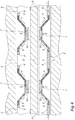
- FIG.1 illustrates the fundamental feature of the novel TEG architecture based on bonding in a flip-chip manner two mirror-like integrated Z-device structures of would be distinct silicon integrated TEGs according to the above identified prior patent application of the same applicant, to form an outstandingly performing bivalve device, once two silicon substrates of integration of the geometrically mirror-like integrated Z-device structures, bonded together are packaged, whereby the perimeter side gaps between the two substrates 1 and 1' of silicon crystal are permanently sealed leaving void internal spaces V of so doubled volume.
- the novel bivalve architecture produces spaced, parallel "double" lines (i.e. an upper and a lower line) of defined tracts or segments of alternately p-doped and n-doped, 4 (4') and 5 (5'), of a polycrystalline semiconductor material, joined by valley bottom and hill-top junction metal contacts 6 (6') and 7 (7'), orthogonally to line arrays of spaced hills 3 (3') having a generally trapezoidal cross section.
- the empty valley spaces V between the spaced hills 3 (3') of the two Z-device structures are evacuated upon packaging a finished TEG device, for substantially eliminating the thermal convection contribution there through to heat transfer from hot junction metal contacts to cold junction metal contacts along by-pass paths rather than in the segments 4 (4') and 5 (5') of alternately p-doped and n-doped polycrystalline semiconductor material of spaced, parallel "double" lines (i.e. an upper and a lower line) of the two counter opposed Z-device structures of the bivalve TEG.
- the hot and cold junctions of a functioning bivalve thermoelectric generator of this disclosure coincide, respectively, with the valley-bottom junction metal contacts 6 of the Z-device structure formed on the silicon substrate 1 and with the valley-bottom junction metal contacts 6'of the Z-device structure formed on the silicon substrate 1'.
- the hill-top junction metal contacts 7 of the Z-device structure formed on the silicon substrate 1 and the hill-top junction metal contacts 7'of the Z-device structure formed on the silicon substrate 1', bonded together in electrical contact, constitute an internal electrical node that may or may not be made connectable to an external load or circuit.
- a modified embodiment of integrated TEG according to this disclosure is illustrated in the cross sectional view of elementary microcells of FIG. 2 .
- broad trenches 9 (9') are etched in the silicon crystal and thereafter filled with a material 8 (8') of higher thermal resistance than silicon, for example silicon nitride, in correspondence with and of width larger than the width of the geometrical projection of the base areas of the hills 3 (3') to be formed on the thin oxide base layer 2 (2').
- a material 8 (8') of higher thermal resistance than silicon for example silicon nitride
- the spacing between adjacent parallel filled trenches may coincide with or just exceed the width of the geometrical projection of the valley-bottom junction metal contacts 6 (6') to be formed over the relatively thin dielectric oxide base layer 2 (2') and over the juxtaposed defined end portions of the oppositely doped segments 4 and 5 (5'and 4') of the deposited thin film of poly crystalline semiconductor.
- the hills 3 (3') formed on the thin oxide base layer 2 (2') may be made of the same high thermal resistance material used as filler 8 (8') in the trenches 9 (9'), for example silicon nitride or of a latticework of nanoscale thin films of phononic silicon.
- the high thermal resistance filler 8 (8') and hills 3 (3') of the same or different high thermal resistance material make the straightforward conduction path of heat flow orthogonal to the plane of the face-to-face coupled Z-device structures of the integrated TEG device, from the hot side to the cold side, more resistive than the paths through the junction metal contacts 6, 7, 7', 6' and the conductive legs 5-4' and 4-5' of the Z-device profile, of doped polycrystalline semiconductor, while the evacuated voids spaces V practically eliminate any convection contribution to a by-pass heat transfer there through.
- FIG. 3 is a cross sectional view of few elementary microcells of an integrated TEG device of this alternative embodiment composed by two dices 1 (1') of monolithically integrated Z-device structures joined together in a face-to-face configuration by a flip-chip bonding technique, reproducing a classical circuit of traditional semiconductor TEGs.
- thermo-electrically generated current is gathered from one or several end pad pairs, the pads of which connect to respective valley-bottom contacts, both belonging to the lower dice 1 (i.e. to the lower Z-device structure) in the drawing, and the open circuit output voltage of the integrated TEG is almost doubled proportionately to an almost doubled temperature difference between hot-side valley-bottom contacts 6' of the upper Z-device structure and cold-side valley-bottom contacts 6 of the lower Z-device structure.
- a sample layout view of the rectangular loop profile of the valley bottom metal contacts 6' of the upper dice 1' is traced directly over the cross section of the contact 7' at the left side of the figure.
- Thermoelectrically generated current i will flow out of a p-doped leg or segment 5 of a string of microcells, constituting the positive terminal of the generator, the negative terminal being a n-doped leg or segment at the other end of the string, both belonging to the Z-device structure of bottom dice 1 .
- FIG. 4 A substantially equivalent embodiment of an integrated bivalve TEG of this disclosure, replicating the classical circuit of traditional semiconductor TEGs, is illustrated in FIG. 4 .
- the structures of the two dices may both have un-split metal contacts 7 and 7' and the necessary electrical insulation and bonding of the two dices may be realized by employing a dummy interposer (or diaphragm), for example a thinned silicon wafer I with oxidized surface layers 2, onto which are defined bond metal pads 10, as required by the aligned-bonding technique of choice being used.
- a dummy interposer or diaphragm
Landscapes
- Chemical & Material Sciences (AREA)
- Inorganic Chemistry (AREA)
- Engineering & Computer Science (AREA)
- Manufacturing & Machinery (AREA)
- Micromachines (AREA)
Description
- This disclosure relates in general to solid state thermoelectric devices, in particular to thermoelectric generators (TEGs) amenable to be fabricated with planar processing technologies and related techniques of heterogeneous or hybrid 3D integration.
- Thermoelectric generators (TEGs) are earnestly investigated as low enthalpy waste heat exploitation devices of outstanding robustness, reliability and virtually unlimited service life, besides being made of environmental friendly materials.
- As power consumption of increasingly popular electronic devices is constantly minimized, TEGs begin to be considered as supplementary power source in conjunction or even in substitution of batteries or other energy storage devices like super-capacitors.
- There is an increasing number of publications concerning thin film technology TEGs exploiting well established processing techniques developed in the Microelectronics and Micro-Electro-Mechanical-Systems (MEMSs), like planar processing, micromachining implant and post implant treatments, flip-chip and bonding techniques and alike.
- The doctorate thesis "Silicon-Micromachined Thermoelectric Generators for Power Generation from hot gas streams" by Israel Boniche, University of Florida, 2010, and "Monolithic integration of VLS silicon nanowires into planar thermoelectric generators" by Diana Davila Pineda, Autonomous University of Barcelona, 2011, offer an extensive introductory review of state-of-the-art practices in the field of thermoelectric devices for solid state heat pumps and power generators.
- The review encompasses also two families of TEGs manufactured with silicon-compatible micro&nano technologies: in devices of a first family heat flow is parallel and in the other family orthogonally to the substrate. The architectures of these integrated TEGs generally comprise a number of unit cells having n-p doped legs, arranged in such a way that the unit cells are thermally in parallel and electrically in series.
- Typically, integrated TEG devices in which heat flows parallel to the substrate may have conductive legs of thermoelectrically active materials deposited over a very high thermal resistance material or a membrane, suspended several hundreds of micrometers above the substrate, or the legs of active materials themselves are freestanding [membrane-less].
- Other relevant examples are reported in :
- ▪ Huesgen, T.; Wois, P.; Kockmann, N. Design and fabrication of MEMS thermoelectric generators with high temperature efficiency. Sens. Actuators A 2008, 145-146, 423-429.
- ▪ .Xie, J.; Lee, C.; Feng, H. Design, fabrication and characterization of CMOS MEMS-based thermoelectric power generators. J. Micromech. Syst. 2010, 19, 317-324.
- ▪ Wang, Z.; Leonov, V.; Fiorini, P.; van Hoof, C. Realization of a wearable miniaturized thermoelectric generator for human body applications. Sens. Actuators A 2009, 156, 95-102.
- ▪ Wang, Z.; Fiorini, P.; Leonov, V.; van Hoof, C. Characterization and optimization of polycrystalline Si70%Ge30% for surface micromachined thermopiles in human body applications. J. Micromech. Microeng. 2009, doi: 10.1088/0960-1317/19/9/094011.
- ▪ Su, J.; Leonov, V.; Goedbloed, M.; van Andel, Y.; de Nooijer, M.C.; Elfrink, R.; Wang, Z.; Vullers, R.J. A batch process micromachined thermoelectric energy harvester: Fabrication and characterization. J. Micromech. Microeng. 2010, doi: 10.1088/0960-1317/20/10/104005.
- ▪ Yang, S.M.; Lee, T.; Jeng, C.A. Development of a thermoelectric energy harvester with thermal isolation cavity by standard CMOS process. Sens. Actuators A 2009, 153, 244-250.
- ▪ Kao, P.-H.; Shih, P.-J.; Dai, C.-L.; Liu, M.-C. Fabrication and characterization of CMOS-MEMS thermoelectric micro generators. .
- ▪ Wang, Z.; van Andel, Y.; Jambunathan, M.; Leonov, V.; Elfrink, R.; Vullers, J.M. Characterization of a bulk-micromachined membrane less in-plane thermopile. J. Electron. Mater. 2011, 40, 499-503.13.
- ▪ Patent
US 7,875,791 B1 "Method for manufacturing a thermopile on a membrane and a membrane-less thermopile, the thermopile thus obtained and a thermoelectric generator comprising such thermopiles" Vladimir Leonov, Paolo Fiorini, Chris Van Hoof (2011) - ▪ Miniaturized thermopile on a membrane are also described by A. Jacquot,W.L Liu, G. Chen,, J.P Fleurial, A. Dauscher, B. Lenoir, in "Fabrication and Modeling of an in-plane thermoelectric micro-generator", Proceedings ICT'02. 21st International Conference on Thermoelectrics, p. 561-564 (2002).
- Other examples of parallel heat flow TEG structures rely on the ability of growing or defining populations of parallel and extremely slender conductors (nanowires) with a mean diameter of few tens of nanometers on a planar substrate of low heat conductivity and in eventually stacking tile-modules to form a thermo-electrical active septum, through which heat flows in the same direction of the parallel nanowires. The articles: "A. I. Hochbaum, R. K. Chen, R. D. Delgado, W. J. Liang, E. C. Garnett, M. Najarian, A. Majumdar, and P. D. Yang, Nature 451, 163-U5 (2008)" and "A. I. Boukai, Y. Bunimovich, J. Tahir-Kheli, J.-K. Yu, W. A. Goddard Iii, and J. R. Heath, Nature 451, 168-171 (2008)";
WO2009/125317 ;EP1,083,610 ;WO2011/007241 ;WO2011/073142 ; offer a review of practices following such an approach. -
US 7,875,791 B1 (by Leonov et al. ) discloses thermopiles that may be supported by a membrane layer or that may be self-supporting. Despite the apparent easy manufacturability of these devices, heat is forced to move in a complicated structure with significant thermal losses. In addition, in some cases adhesive are needed in order to assure thermal contact to a heat source at the top or the bottom surface of the initial substrate. This results in thermal coupling at system level, lossy thermal paths and mechanical fragilities, all features that that penalize performance of the thermopile. - A second family of TEG devices is often referred to as "out-of-plane" heat flux TEGs. They are characterized by the fact that heat flows orthogonally to the substrate. In these devices the thermoelectrically active materials are usually laid on or are part of high aspect-ratio supporting structures standing onto the substrate. Despite a more sophisticated and apparently expensive fabrication process, this configuration minimizes thermal losses, simplifies thermal coupling at system level enhancing overall performance.
- Being manufactured by conventional CMOS\BiCMOS\MEMs materials and processes, the "out-of-plane" heat flux TEGs are amenable to miniaturization and integration in microelectronic and optoelectronic devices, among other applications.
- Examples are reported by M. Strasser et al. in "Miniaturized Thermoelectric Generators Based on Poly-Si and Poly-SiGe Surface Micromachining", (presented in The 11th International Conference on Solid-State Sensors and Actuators, Munich, Germany, June 10-14, 2001) and "Micromachined CMOS Thermoelectric Generators as On-Chip Power Supply" (presented in The 12th International Conference on Solid-State Sensors and Actuators and Microsystems, Boston, USA, June 8-12, 2003) .
JP10303469 - Out-of-plane or orthogonal heat flux thin film structures are useful for innumerable applications, for example for micro power generation or for temperature management in complex integrated systems, for energy recovery or harvesting.
- Electric power yield from a given heat flow and electric power yield versus the footprint area of out-of-plane or orthogonal heat flux devices of the prior art, based on a common semiconductor or any material compatible with ICs fabrication processes, are yet poor and there is a need of more efficient and power intensive devices.
- A significantly increased power yield per unit of footprint area of an integrated TEG and an enhanced conversion efficiency is achieved with a novel out-of-plane (i.e. orthogonal) heat flux, Z-device structure as defined in the appended claims. In the ensuing description reference will be made to a cell of a Z-device structure, which comprises: a substrate wafer, hill-top junction metal contacts and valley-bottom junction metal contacts joining juxtaposed ends of segments, alternately p-doped and n-doped, of defined thin film lines of segments of a polycrystalline semiconductor, extending over inclined opposite flanks of hills of a material of lower thermal conductivity than the thermal conductivity of said polycrystalline semiconductor, said material of lower thermal conductivity forming valleys and said hills.
- In the TEG architecture of this disclosure, the internal by-pass heat transfer by heat conduction normally occurring through a dielectric filler (e.g. silicon oxide) deposited in the valleys over defined tracts or segments of sequentially alternated p-type and n-type deposited semiconductor thin-film and over metal bridges that provide electrical continuity between juxtaposed ends of defined segments of p-type and of n-type semiconductor at valley bottom junctions, between spaced hills of trapezoidal cross section, on opposite slanted flanks of which lay the defined semiconductor thin-film legs of a unit cell of a typical Z-device profile, is significantly reduced by realizing junction metal contacts of relatively low profile (i.e. low aspect ratio) and reduced encumbrance and leaving void the valley spaces, no longer filled with a dielectric material nor hosting metal bridges of high aspect ratio of electrical connection of juxtaposed ends of a p-type and an n-type leg. Preferably the internal void spaces are evacuated upon packaging the finished device.
- Such an efficiency enhancing feature is best exploited, according to this disclosure, by delimiting these internal voids of the multi-cellular integrated Z-device structure formed over a silicon wafer of substrate, not by a passive planar cover bonded over the hill-top junction metal contacts, but by a capping element in form of a geometrically identical mirror-like integrated structure duplicated on the same or on a second silicon wafer substrate.
- According to a first embodiment of this disclosure, the two geometrically identical integrated Z-device structures, integrated in two distinct silicon dices, may have an inverted type of conductivity of the defined tracts or segments of the lines of thin film polycrystalline semiconductor, and are joined together in a face-to-face configuration by common flip-chip bonding technique or similar (i.e.wafer-to-wafer bonding), such that a p-doped thin film leg of one structure faces toward a n-doped thin film leg of the other structure and vice versa.
- Upon joining the two mirror-like Z-device structures together, the hill-top metal contacts of one integrated structure may be bonded in electrical and thermal continuity with correspondent hill-top metal contacts of the other integrated structure, forming a substantially "bivalve" (mirror-like structure) TEG of increased power yield for the same footprint area and having an enhanced conversion efficiency because of a further reduced internal by-pass of heat by irradiation in consideration of an augmented internal empty space.
- The thermo-electrically generated current may be gathered from one or several end pad pairs, the pads of which are connected to respective valley bottom contacts, on one and on the other of the two dices of the bivalve device, at the ends of conductive lines of micro cells respectively belonging to one and to the other of the two coupled dices.
- According to an alternative embodiment, electrically reproducing the classical circuit of traditional semiconductor TEGs, the thermo-electrically generated current may be gathered from one or several end pad pairs, the pads of which connect to respective valley bottom contacts, belonging both to one of the two coupled dices of the bivalve device. In this case, there is a mirror-like condition of the two coupled dices as far as the type of conductivity of counter-opposed segments of the thin film semiconductor lines is concerned, whilst the hill-top metal contacts are split in two electrically separated parts in order to electrically connect segments of same type of conductivity belonging to one and to the other dice, respectively at one and at the other side of the hill-top, and the valley bottom contacts of one of the two dices extends itself around the perimeter at the base respective hill for connecting the other ends of the conductive segments connected by the two parts of the split hill-top contacts.
- Alternatively, instead of bonding hill-top metal contacts by flip-chip bonding technique, the structures of the two dices may both have un-split metal contacts and the two dices be mechanically bonded with metal bond pads defined over the surfaces of both sides of an electrically insulating interposer, for example a thinned silicon wafer with oxidized surfaces.
-
-
FIG. 1 is a cross sectional view of few elementary microcells of an integrated TEG of this disclosure composed by two monolithically integrated Z-device dices of identical mirror-like geometry but with inverted type of conductivity of the defined segments of the lines of thin film semiconductor, joined together in a face-to-face configuration by a flip-chip bonding technique, according to a first embodiment. -
FIG. 2 is a cross sectional view of few elementary microcells of an integrated TEG of this disclosure, according to another embodiment. -
FIG. 3 is a cross sectional view of few elementary microcells of an integrated TEG of this disclosure composed by two monolithically integrated Z-device dices joined together in a face-to-face configuration by a flip-chip bonding technique, according to an alternative embodiment, reproducing a classical circuit of traditional semiconductor TEGs. -
FIG. 4 is a cross sectional view of an alternative manner in which the classical circuit of traditional semiconductor TEGs may be realized. - With reference to the drawings, the geometrical mirror-like character of the two dices of monolithic integration of a multi-cellular Z-device structure, bonded together by a common flip-chip technique or equivalent technique, to compose a bivalve, double Z-device structure of a TEG device of this disclosure, is remarked by using the same reference numerals for indicating the same functional parts of the Z-device structures (primed for those belonging to the upper dice).
- Commercially available silicon wafers of any size and having a thickness generally not exceeding 675 micrometers (µm) may be used.
- With reference to
FIG. 1 , a dielectric base layer 2 (2') of substantially uniform thickness that may be generally comprised between 1 nanometer (nm) and 1 micrometer (µm), preferably of about 10 nm, provides a necessary bottom electrical insulation at the surface of the substrate wafer 1 (1') without introducing a significant thermal resistance. - According to well established techniques of micro-machining processing, parallel lines or other arrangement of spaced hills 3 (3') of a relatively low thermal conductivity material such as, for example, of thick oxide successively grown or deposited over unmasked areas of a firstly grown base layer 2 (2'), up to a height that generally may be comprised between 0,1 and 50 µm. The typical inclined flanks of the hills 3 (3') define valleys there between, the substantially planar bottom of which generally may have a width comprised between 0,1 and 100 µm, most preferably between 0.2 and 50 µm, similarly to the width of the top of the hills 3 (3').
- Alternatively, the hills 3 (3') may be defined starting from a layer of deposited oxide or other material such as silicon nitride, through a succession of masking and etching steps, under controlled isotropic etching conditions, in order to slant the walls of the progressively etched valleys toward a substantially flat bottom by an angle of inclination from the base plane that preferably is comprised between 45 and 85 degrees.
- LPCVD silicon oxide, deposited with varying amounts of phosphorous and/or hydrogen impurities and specific processing and post processing conditions promoting structural disorder (re: Y. S. Ju and K. E. Goodson,"Process-dependent thermal transport properties of silicon-dioxide films deposited using low-pressure chemical vapor deposition", AIP Journal of Applied Physics, Volume 85, ) is also an effective material with which hills 3 (3') of enhanced resistance to heat conduction may be formed over the oxidized surface of the substrate wafer 1 (1'). Yet another alternative material with which
hills 3 of enhanced resistance to heat conduction may be formed over an oxidized surface of the substrate wafer 1 (1') is the family of nanomesh structures of phononic silicon (re:"Reduction of thermal conductivity in phononic nanomesh structures" by Jen-Kan Yu, S. Mitrovic, D. Tham, J. Varghese and J.R. Heath, Nature Nanotechnology, Vol. 5, October 2010, ©2010 Macmillan Publishers Lim.). - The material with which the hills 3 (3') can be made, must have a low thermal conductivity , significantly lower than the thermal conductivity of the material of the p-type and n-type legs of conductive material supported thereon, in order to further penalize by-pass paths of heat flow alternative to the paths of productive heat conduction along the polycrystalline doped semiconductor thin film segments or legs 4, 5 (4', 5') defined over opposite slanted surfaces of truncated rectangular pyramid shaped hills 3 (3') or of hills with a trapezoidal cross section along one axis and straight sides or flanks orthogonal to it.
- Examples of suitable materials of lower thermal conductivity than the thermal conductivity of a thermoelectrically active polycrystalline semiconductor and their respective heat conduction coefficients are reported in the following table.
Material Thickness [nm] Thermal Conductivity [W m-1 K-1] Thermal SiO2 .> 250 ∼ 1.2 SiO2(PECVD@300C) 30 -50 0.82 ± 0.02 SiO2(PECVD@300C) 90 -180 1.00 ± 0.10 SiO2(PECVD@300C) >200 ∼1.2 (Bulk) SiNx(PECVD@300C) 20 -40 0.55 ± 0.05 SiNx (PECVD@300C) 60 -120 0.65 ± 0.05 SiNx (APCVD@900C) 180 ∼1.45 - Hills 3 (3') of a superlattice of nanoscale thin films of phononic silicon realized over a dielectric base layer on the surface of the substrate is another alternative capable of markedly reducing the thermal conductivity of the hills 3 (3') of the integrated TEG structure,.
- Defined tracts or segments of alternately p-doped and n-doped, 4 (4') and 5 (5'), respectively, of parallel lines of a polycrystalline semiconductor material such as, for example, doped Si or SiGe, deposited in form of a thin film of substantially uniform thickness over the bottom isolation dielectric 2 (2') and the spaced hills 3 (3'), constitute the two legs of thermoelectric material that electrically connect a junction at the valley bottom to the two adjacent junctions on top of the hills 3 (3') (i.e. a unit or elementary cell of a Z-device structure). The deposited doped polycrystalline silicon layer of the segments 4 (4') and 5 (5') may have thickness, generally comprised between 10 and 1000 nm, but may even be as thick as one or more micrometers, depending on contemplated applications, scaling of the elementary cell structure, properties of the polycrystalline semiconductor material used and design choices of the integrated TEG.
- Physically, the junctions, respectively at valley bottoms and at hill-tops or vice versa, are both constituted bysuitable metal contacts, respectively 6 (6') and 7 (7'), electrically bridging an interruption gap between the defined end of a p-doped segment or leg 5 (5') and the defined end of a n-doped thermoelectric segment or leg 4 (4') of polycrystalline thin-film semiconductor in order to avoid formation of p-n junctions along the string of elementary integration modules or cells in series of an electrically conductive line (chain) of cells.
- The deposited metal layer of the junction metal contacts 6 (6') and 7 (7') that extend over and in electrical contact with the end portions of the two segments 4 (4') and 5 (5') of polycrystalline semiconductor, for a good part of their portions laying onto the substantially planar valley bottoms and hill-tops, may be of thickness ranging from about 0,1 to about 5 µm.
- The cross sectional views of the drawings well represent the characteristic Z profile of the conductive legs 4 (4') and 5 (5') of thermoelectric material of the elementary cells.
- Preferably, there is a multi-layer interfacing between the metal and the polycrystalline semiconductor thin film that is used to control the electrical interface resistance between the metal and the semiconductor materials and eventually disproportionate electrical conductivity versus thermal conductivity for reducing heat conduction toward the metallic bulk of the metal contacts, namely, the valley bottom contacts 6 (6') and the hill-top contacts 7 (7'). As shown in the enlargement lens, an effective interfacing multi-layer may comprise a 1-50 nm film (6a) of a silicide belonging to the group: TiSi2, WSi2, MoSi2, PtSi2 and CoSi2, in contact with the polycrystalline doped semiconductor, an intermediate 1-10 nm film 6b of W or Ti and a 5-30 nm thick film 6c of TiN in contact with the metal layer 6 (6') and 7 (7') of A1 or of Al-Si alloy or copper.
- In the novel integrated out-of-plane flux, bivalve TEG structure of this disclosure, among parallel lines or other arrangement of spaced hills 3 (3') there are void valley spaces V of doubled volume compared to those of the TEG structure described in prior Italian patent application No.
MI2014-A-001637 WO2016/046713 A1 , of the same applicant, are created upon bonding together two halves of substantially mirror-like geometry as depicted in the drawings. - Flip-chip aligned bonding, may be carried out on the processed wafers from which TEG device dices are successively cut to be packaged or on cut dices thereof. Generally, depending on the specific application, aligned bonding for realizing the TEG devices of this disclosure may be carried out in chip-to-chip, chip-to-wafer or wafer-to-wafer mode.
- According to the embodiment of
FIG. 1 , in the novel TEG architecture, are the planar surfaces of the hill-top metal contacts 7 and 7' of the two mirror-like Z-device structures realized on the same or on distinct silicon wafers ofsubstrate 1 and 1', that are bonded together in electrical contact according to one of the many flip-chip bonding techniques, preferably using an aligned-bonding technique of thermo-compressive metal-to-metal bonding: Cu-Cu,W-W, Ti-Ti ..etc., with or without diffusion layers, after a CMP planarization, or via plasma bonding (Y-Ox/Y-Ox), PECVD SiO2-SiO2, benzocyclobutene (BCB) to BCB bonding. Hybrid bonding techniques such as BCB and a variety of polymers or polymides, metal layers such Ti films and inter-metallic compounds (IMCs), Cu-Sn Solid-Liquid-Interdiffusion (SLID) bonding, Au-Sn or Au-In eutectic bonding, may alternately be used as well as anodic bonding or micro-bump stacking. - Preferably, after devices manufacturing, both the top and
bottom wafers 1 and 1' may be subjected to backside thinning process aiming to reduce the thickness of commercial wafers, including mechanical or chemical treatments, such as mechanical grinding, dry polishing, chemical-mechanical grinding, spin etching chemical-mechanical polishing and plasma dry etching. The aim is to reduce the original thickness to less than 100 µm or to ultrathin values of less than 40 µm. Thinning of the wafers reduces overall thermal resistance of the integrated out-of-plane bivalve TEG structure and makes it amenable to be deployed in next generation 3D integrated circuit. - The manner in which spaced parallel electrically conductive lines of defined tracts or segments of alternately p-doped and n-doped, 4 (4') and 5 (5'), of a polycrystalline semiconductor material, joined by valley-bottom and hill-top junction metal contacts 6 (6') and 7 (7') are created, orthogonally extending in respect to line arrays of spaced hills 3 (3') made of a material of higher thermal resistance than the thermal resistance of the thermoelectrically active polycrystalline semiconductor, over the slanted opposite sides of which are defined the segments 4 (4') and 5 (5'), may be immediately recognized by any ordinarily skilled person in CMOS or BiCMOS process technologies.
- The width of the parallel spaced conductive lines (i.e. of the segments 4 (4') and 5 (5')) may be generally comprised between 0.1 and 500 µm, preferably between 0.5 and 10 µm.
-
FIG.1 illustrates the fundamental feature of the novel TEG architecture based on bonding in a flip-chip manner two mirror-like integrated Z-device structures of would be distinct silicon integrated TEGs according to the above identified prior patent application of the same applicant, to form an outstandingly performing bivalve device, once two silicon substrates of integration of the geometrically mirror-like integrated Z-device structures, bonded together are packaged, whereby the perimeter side gaps between the twosubstrates 1 and 1' of silicon crystal are permanently sealed leaving void internal spaces V of so doubled volume. - In practice, as may be observed from the cross-sectional view of
FIG. 1 , depicting the cross section of a full microcell and by the adjacent semi-portions of a repetitive multi-cellular structure, the novel bivalve architecture produces spaced, parallel "double" lines (i.e. an upper and a lower line) of defined tracts or segments of alternately p-doped and n-doped, 4 (4') and 5 (5'), of a polycrystalline semiconductor material, joined by valley bottom and hill-top junction metal contacts 6 (6') and 7 (7'), orthogonally to line arrays of spaced hills 3 (3') having a generally trapezoidal cross section. - Preferably the empty valley spaces V between the spaced hills 3 (3') of the two Z-device structures are evacuated upon packaging a finished TEG device, for substantially eliminating the thermal convection contribution there through to heat transfer from hot junction metal contacts to cold junction metal contacts along by-pass paths rather than in the segments 4 (4') and 5 (5') of alternately p-doped and n-doped polycrystalline semiconductor material of spaced, parallel "double" lines (i.e. an upper and a lower line) of the two counter opposed Z-device structures of the bivalve TEG.
- Differently from known silicon integrated TEGs based on the so-called Z-device structure and from the TEGs of the above identified prior patent application of the same applicant, the hot and cold junctions of a functioning bivalve thermoelectric generator of this disclosure coincide, respectively, with the valley-bottom
junction metal contacts 6 of the Z-device structure formed on thesilicon substrate 1 and with the valley-bottom junction metal contacts 6'of the Z-device structure formed on the silicon substrate 1'. - According to this embodiment, the hill-top
junction metal contacts 7 of the Z-device structure formed on thesilicon substrate 1 and the hill-top junction metal contacts 7'of the Z-device structure formed on the silicon substrate 1', bonded together in electrical contact, constitute an internal electrical node that may or may not be made connectable to an external load or circuit. - A modified embodiment of integrated TEG according to this disclosure is illustrated in the cross sectional view of elementary microcells of
FIG. 2 . - Prior to forming a thin oxide base layer 2 (2') over the silicon wafer 1 (1'), broad trenches 9 (9') are etched in the silicon crystal and thereafter filled with a material 8 (8') of higher thermal resistance than silicon, for example silicon nitride, in correspondence with and of width larger than the width of the geometrical projection of the base areas of the hills 3 (3') to be formed on the thin oxide base layer 2 (2').
- Practically, the spacing between adjacent parallel filled trenches may coincide with or just exceed the width of the geometrical projection of the valley-bottom junction metal contacts 6 (6') to be formed over the relatively thin dielectric oxide base layer 2 (2') and over the juxtaposed defined end portions of the oppositely doped segments 4 and 5 (5'and 4') of the deposited thin film of poly crystalline semiconductor.
- The hills 3 (3') formed on the thin oxide base layer 2 (2') may be made of the same high thermal resistance material used as filler 8 (8') in the trenches 9 (9'), for example silicon nitride or of a latticework of nanoscale thin films of phononic silicon.
- The high thermal resistance filler 8 (8') and hills 3 (3') of the same or different high thermal resistance material, make the straightforward conduction path of heat flow orthogonal to the plane of the face-to-face coupled Z-device structures of the integrated TEG device, from the hot side to the cold side, more resistive than the paths through the
junction metal contacts - According to alternative embodiments of a tri-dimensionally integrated bivalve TEG architecture of this disclosure, the classical circuit of traditional semiconductor TEGs may be replicated.
-
FIG. 3 is a cross sectional view of few elementary microcells of an integrated TEG device of this alternative embodiment composed by two dices 1 (1') of monolithically integrated Z-device structures joined together in a face-to-face configuration by a flip-chip bonding technique, reproducing a classical circuit of traditional semiconductor TEGs. - In such an alternative embodiment, the thermo-electrically generated current is gathered from one or several end pad pairs, the pads of which connect to respective valley-bottom contacts, both belonging to the lower dice 1 (i.e. to the lower Z-device structure) in the drawing, and the open circuit output voltage of the integrated TEG is almost doubled proportionately to an almost doubled temperature difference between hot-side valley-bottom contacts 6' of the upper Z-device structure and cold-side valley-
bottom contacts 6 of the lower Z-device structure. - For replicating the classical circuit of traditional discrete semiconductor TEGs, there is a mirror-like condition of the two coupled dices, as far as the type of conductivity of counter-opposed defined segments 4-4' and 5-5' is concerned, of the conductive lines of semiconductor thin film, whilst the flip-chip bonded hill-top metal contacts 7 (7') are split in two electrically separated parts in order to electrically connect segments of same type of conductivity belonging to one and to the other dice, respectively at one and at the other side of the hill-top surface, and the valley bottom contacts 6' of the upper dice 1' extend themselves around the perimeter at the base of a respective hill 3' for connecting together the other ends of the conductive segments of opposite type of conductivity respectively connected by one and the other part of the split metal contact 7' at the hill-top of the same hill 3'.
- A sample layout view of the rectangular loop profile of the valley bottom metal contacts 6' of the upper dice 1' is traced directly over the cross section of the contact 7' at the left side of the figure.
- Thermoelectrically generated current i will flow out of a p-doped leg or
segment 5 of a string of microcells, constituting the positive terminal of the generator, the negative terminal being a n-doped leg or segment at the other end of the string, both belonging to the Z-device structure ofbottom dice 1 . - A substantially equivalent embodiment of an integrated bivalve TEG of this disclosure, replicating the classical circuit of traditional semiconductor TEGs, is illustrated in
FIG. 4 . - Instead of bonding hill-
top metal contacts 7 and 7'defined in two separate parts by a flip-chip bonding technique as in the embodiment ofFIG. 3 , the structures of the two dices may both haveun-split metal contacts 7 and 7' and the necessary electrical insulation and bonding of the two dices may be realized by employing a dummy interposer (or diaphragm), for example a thinned silicon wafer I with oxidized surface layers 2, onto which are definedbond metal pads 10, as required by the aligned-bonding technique of choice being used.
Claims (9)
- A mirror-like, integrated thermoelectric generator device of out-of-plane heat flux configuration comprising:a) first and second silicon dice (1, 1') of a same processed silicon wafer or of distinctly processed silicon wafers having a dielectric base layer (2, 2') on at least a surface and a multi cellular Z-device structure on said base layers (2, 2');b) line arrays of mirror-like identical geometry, of spaced hills (3, 3') of a material of low thermal conductivity over said dielectric base layers (2, 2') of both dices (1, 1');c) parallel lines of segments (4, 4', 5, 5'), alternately p-doped and n-doped, of a deposited and defined thin film of polycrystalline semiconductor, extending orthogonally to said line arrays of spaced hills (3, 3'), over inclined flanks of said spaced hills and partly over planar tops of the hills and planar valleys between inclined flanks of adjacent hills;d) hill-top junction metal contacts (7, 7') and valley-bottom junction metal contacts (6, 6') electrically joining juxtaposed ends of segments (4, 4', 5, 5') of said thin film lines of polycrystalline semiconductor;the thermal conductivity of said material of low thermal conductivity being lower than said doped polycrystalline semiconductor; said first and second dice (1, 1') being joined together in a face-to-face configuration according to a flip-chip aligned-bonding of the hill-top metal contacts (7) of the multi cellular Z-device structure of the first dice (1) counter opposed to corresponding hill-top metal contacts (7') of the multi cellular Z-device structure of the second dice (1');
the valley-bottom metal contacts (6') of the multi cellular Z-device structure of one dice constituting hot junctions and the valley-bottom metal contacts of the multi cellular Z-device structure of the other dice (6) constituting cold junctions of the functioning thermoelectric generator. - The mirror-like thermoelectric generator device of claim 1, wherein void spaces (V) among said spaced hills (3, 3') are permanently sealed by occlusion of side gaps between the coupled dice (1,1').
- The mirror-like thermoelectric generator of claim 2, wherein said spaces (V) are under vacuum.
- The mirror-like thermoelectric generator device of claim 1, further comprising regularly spaced trenches (9, 9'), etched in the silicon wafers, filled with a material of lower thermal conductivity(8, 8'), than silicon in correspondence with a geometrical projections of the bases of said spaced hills (3, 3') to be formed on said dielectric base layer (2, 2');
the width of said trenches (9, 9') exceeding the width of the geometrical projection of the base areas of said hills (3, 3') leaving a spacing between adjacent trenches equal to or slightly larger than the width of the geometrical projection of said valley-bottom junction metal contacts (6, 6'). - The mirror-like thermoelectric generator device of claim 4, wherein said material of lower thermal conductivity is silicon nitride.
- The mirror-like thermoelectric generator device of claim 5, wherein said hills (3, 3') are of a material belonging to the group of thermally grown silicon oxide, deposited silicon oxides, silicon nitride, latticework of nanoscale thin films of phononic silicon.
- The mirror-like thermoelectric generator device of any of the preceding claims, wherein said first (1) and second (1') dice with multi cellular Z-device structures of mirror-like geometries, have offset sequences of alternately p-doped and n-doped defined segments (4, 5, 4', 5') of polycrystalline semiconductor such that, upon bonding, any p-doped segment faces toward an n-doped segment and vice versa.
- The mirror-like thermoelectric generator device of any of the claims from 1 to 6, wherein said first (1) and second (1') dice with multi cellular Z-device structures of mirror-like geometries, have mirror like sequences of alternately p-doped and n-doped defined segments (4, 4', 5, 5') of polycrystalline semiconductor such that, upon bonding, any p-doped segment faces toward an p-doped segment and any n-doped segment faces toward an n-doped segment;
said flip-chip bonded counter opposed hill-top metal contacts (7, 7') are split in two electrically separated parts, each part electrically connecting segments of same type of conductivity belonging to one and to the other dice (1, 1'), respectively at one and at the opposite side of the hill-tops; and
the valley-bottom contacts (6') of one (1') of the two dice extend themselves around the perimeter at the base of a respective hill (3') for connecting together the other ends of the conductive segments (4', 5') of opposite type of conductivity respectively connected by one and the other part of the split metal contact (7') at the hill-top of said hill (3'). - The mirror-like thermoelectric generator device of any of the claims from 1 to 6, wherein said first (1) and second (1'), dice of identical mirror-like geometries, have mirror like sequences of alternately p-doped and n-doped defined segments (4, 4', 5, 5') of polycrystalline semiconductor such that, upon bonding, any p-doped segment faces toward an p-doped segment any n-doped segment faces toward an n-doped segment;
said hill-top metal contacts (7, 7') electrically connecting segments of opposite type of conductivity belonging to a respective dice (1, 1') are mechanically flip-chip bonded to bond metal pads (10) defined onto opposite surfaces of an interposer (I) of electrical insulation; and
the valley bottom contacts (6') of one (1') of the two dice extend themselves around the perimeter at the base of a respective hill (3') for connecting together the other ends of the conductive segments (4', 5') of opposite type of conductivity respectively connected together by a metal contacts (7') at the hill-top of said hill (3').
Applications Claiming Priority (2)
| Application Number | Priority Date | Filing Date | Title |
|---|---|---|---|
| ITMI20141712 | 2014-10-01 | ||
| PCT/IB2015/057325 WO2016051313A1 (en) | 2014-10-01 | 2015-09-23 | Silicon integrated bivalve thermoelectric generator of out-of-plane heat flux configuration |
Publications (2)
| Publication Number | Publication Date |
|---|---|
| EP3201955A1 EP3201955A1 (en) | 2017-08-09 |
| EP3201955B1 true EP3201955B1 (en) | 2018-07-25 |
Family
ID=52000938
Family Applications (1)
| Application Number | Title | Priority Date | Filing Date |
|---|---|---|---|
| EP15781434.4A Not-in-force EP3201955B1 (en) | 2014-10-01 | 2015-09-23 | Silicon integrated mirror-like thermoelectric generator of out-of-plane heat flux configuration |
Country Status (5)
| Country | Link |
|---|---|
| US (1) | US10003002B2 (en) |
| EP (1) | EP3201955B1 (en) |
| JP (1) | JP6862339B2 (en) |
| CN (1) | CN106716658B (en) |
| WO (1) | WO2016051313A1 (en) |
Families Citing this family (3)
| Publication number | Priority date | Publication date | Assignee | Title |
|---|---|---|---|---|
| CN108287027A (en) * | 2017-12-29 | 2018-07-17 | 华中科技大学 | A kind of film-type superhigh temperature heat flow transducer sensitivity member and preparation method thereof |
| KR102474817B1 (en) * | 2018-12-04 | 2022-12-06 | 현대자동차주식회사 | Thermoelectric module and apparatus for modulating a temperature including thereof |
| JP2021090001A (en) * | 2019-12-05 | 2021-06-10 | 国立大学法人大阪大学 | Thermoelectric conversion device, manufacturing method of thermoelectric conversion device, and electric device |
Family Cites Families (21)
| Publication number | Priority date | Publication date | Assignee | Title |
|---|---|---|---|---|
| JPH04101472A (en) * | 1990-08-20 | 1992-04-02 | Matsushita Electric Ind Co Ltd | Cooler |
| JPH10303469A (en) * | 1997-04-23 | 1998-11-13 | Sharp Corp | Thin-film thermoelectric conversion element, semiconductor device using the same, and printed circuit board using the same |
| CN100385694C (en) | 1999-03-10 | 2008-04-30 | 日立金属株式会社 | Thermoelectric conversion material and method for producing same |
| JP4669395B2 (en) * | 2003-06-30 | 2011-04-13 | 株式会社ダ・ビンチ | Peltier device and manufacturing method thereof |
| JP4401754B2 (en) * | 2003-11-28 | 2010-01-20 | 清仁 石田 | Method for manufacturing thermoelectric conversion module |
| JP2005259944A (en) * | 2004-03-11 | 2005-09-22 | Nagoya Industrial Science Research Inst | Thin film thermoelectric semiconductor device and manufacturing method thereof |
| JP4422548B2 (en) * | 2004-05-17 | 2010-02-24 | 学校法人立命館 | Thermoelectric conversion device |
| US7299639B2 (en) | 2004-06-22 | 2007-11-27 | Intel Corporation | Thermoelectric module |
| KR100668610B1 (en) * | 2004-09-09 | 2007-01-16 | 엘지전자 주식회사 | Thin film thermoelectric module |
| US7531739B1 (en) * | 2004-10-15 | 2009-05-12 | Marlow Industries, Inc. | Build-in-place method of manufacturing thermoelectric modules |
| US7544883B2 (en) * | 2004-11-12 | 2009-06-09 | International Business Machines Corporation | Integrated thermoelectric cooling devices and methods for fabricating same |
| JP2006196577A (en) * | 2005-01-12 | 2006-07-27 | Hitachi Ltd | Method for producing oriented thermoelectric thin film and semiconductor device having oriented thermoelectric thin film |
| EP1976034A3 (en) | 2007-03-29 | 2011-11-09 | Stichting IMEC Nederland | Method for manufacturing a thermopile, the thermopile thus obtrained and a thermoelectric generator comprising such thermopiles |
| DE102008009428A1 (en) * | 2008-02-15 | 2009-08-27 | Isabellenhütte Heusler Gmbh & Co. Kg | Thermoelectric converter and associated manufacturing method |
| ITRM20080193A1 (en) | 2008-04-11 | 2009-10-12 | Univ Milano Bicocca | THERMO-ELECTRIC BIDIRECTIONAL CONVERSION DEVICE WITH EFFECT SEEBECK / PELTIER USING NANOFILES OF CONDUCTOR OR SEMICONDUCTOR MATERIAL. |
| IT1397598B1 (en) | 2009-07-15 | 2013-01-16 | Univ Milano Bicocca | THERMO-ELECTRIC CONVERSION DEVICE WITH EFFECT SEEBECK / PELTIER USING STRUCTURES OF SEMICONDUCTIVE MATERIAL TREATED NOT REQUESTING DEFINITION ON NANOMETRIC SCALE |
| IT1397679B1 (en) | 2009-12-15 | 2013-01-18 | Univ Milano Bicocca | THERMO-ELECTRIC CONVERSION ELEMENT SEEBECK / PELTIER INCLUDING PARALLEL NANOFILES OF CONDUCTOR OR SEMICONDUCTOR MATERIALS ORGANIZED IN FILE AND COLUMNS THROUGH AN INSULATING BODY AND PROCEDURE |
| US9444027B2 (en) * | 2011-10-04 | 2016-09-13 | Infineon Technologies Ag | Thermoelectrical device and method for manufacturing same |
| US20130307200A1 (en) * | 2011-11-02 | 2013-11-21 | John Carberry | Sintered Polycrystalline Silicon-based Thermoelectrics |
| US9123780B2 (en) | 2012-12-19 | 2015-09-01 | Invensas Corporation | Method and structures for heat dissipating interposers |
| US9620698B2 (en) * | 2013-01-08 | 2017-04-11 | Analog Devices, Inc. | Wafer scale thermoelectric energy harvester |
-
2015
- 2015-09-23 JP JP2017517685A patent/JP6862339B2/en not_active Expired - Fee Related
- 2015-09-23 CN CN201580052881.4A patent/CN106716658B/en not_active Expired - Fee Related
- 2015-09-23 EP EP15781434.4A patent/EP3201955B1/en not_active Not-in-force
- 2015-09-23 WO PCT/IB2015/057325 patent/WO2016051313A1/en not_active Ceased
-
2017
- 2017-03-21 US US15/464,987 patent/US10003002B2/en active Active
Non-Patent Citations (1)
| Title |
|---|
| None * |
Also Published As
| Publication number | Publication date |
|---|---|
| JP6862339B2 (en) | 2021-04-21 |
| JP2017537460A (en) | 2017-12-14 |
| CN106716658A (en) | 2017-05-24 |
| EP3201955A1 (en) | 2017-08-09 |
| CN106716658B (en) | 2019-03-08 |
| US10003002B2 (en) | 2018-06-19 |
| US20170194550A1 (en) | 2017-07-06 |
| WO2016051313A1 (en) | 2016-04-07 |
Similar Documents
| Publication | Publication Date | Title |
|---|---|---|
| EP3198648B1 (en) | Silicon integrated, out-of-plane heat flux thermoelectric generator | |
| US9997691B2 (en) | 3D integrated thermoelectric generator operating in an out-of-plane heat flux configuration with internal voids and heat conduction paths conditioning vias | |
| EP3533085B1 (en) | Integrated thermoelectric generator and related method of fabrication | |
| US20090000652A1 (en) | Thermoelectric Structures Including Bridging Thermoelectric Elements | |
| WO2013127114A1 (en) | Miniature thermoelectric energy collector and manufacturing method therefor | |
| US10003002B2 (en) | Silicon integrated bivalve thermoelectric generator of out-of-plane heat flux configuration | |
| WO2010114766A2 (en) | Thermoelectric devices including thermoelectric elements having off-set metal pads and related structures, methods, and systems | |
| KR20120046106A (en) | Microstructure for a seebeck effect thermoelectric generator, and method for making such a microstructure | |
| WO2013127113A1 (en) | Three-dimensional thermoelectric energy collector and manufacturing method therefor | |
| US11276810B2 (en) | Method of producing a flexible thermoelectric device to harvest energy for wearable applications | |
| US20140130839A1 (en) | Structure useful for producing a thermoelectric generator, thermoelectric generator comprising same and method for producing same | |
| US10388845B2 (en) | Thermoelectric generator | |
| Iulianella et al. | Integrated Thermoelectric Generator and related Method of Fabrication |
Legal Events
| Date | Code | Title | Description |
|---|---|---|---|
| PUAI | Public reference made under article 153(3) epc to a published international application that has entered the european phase |
Free format text: ORIGINAL CODE: 0009012 |
|
| 17P | Request for examination filed |
Effective date: 20170419 |
|
| AK | Designated contracting states |
Kind code of ref document: A1 Designated state(s): AL AT BE BG CH CY CZ DE DK EE ES FI FR GB GR HR HU IE IS IT LI LT LU LV MC MK MT NL NO PL PT RO RS SE SI SK SM TR |
|
| AX | Request for extension of the european patent |
Extension state: BA ME |
|
| RIN1 | Information on inventor provided before grant (corrected) |
Inventor name: BUOSCIOLO, ANTONIETTA Inventor name: GAMMARIELLO, GIUSEPPE Inventor name: MASCOLO, DANILO Inventor name: GISON, ITALO |
|
| DAV | Request for validation of the european patent (deleted) | ||
| DAX | Request for extension of the european patent (deleted) | ||
| GRAP | Despatch of communication of intention to grant a patent |
Free format text: ORIGINAL CODE: EPIDOSNIGR1 |
|
| INTG | Intention to grant announced |
Effective date: 20180206 |
|
| GRAS | Grant fee paid |
Free format text: ORIGINAL CODE: EPIDOSNIGR3 |
|
| GRAA | (expected) grant |
Free format text: ORIGINAL CODE: 0009210 |
|
| AK | Designated contracting states |
Kind code of ref document: B1 Designated state(s): AL AT BE BG CH CY CZ DE DK EE ES FI FR GB GR HR HU IE IS IT LI LT LU LV MC MK MT NL NO PL PT RO RS SE SI SK SM TR |
|
| REG | Reference to a national code |
Ref country code: GB Ref legal event code: FG4D |
|
| REG | Reference to a national code |
Ref country code: CH Ref legal event code: EP |
|
| REG | Reference to a national code |
Ref country code: AT Ref legal event code: REF Ref document number: 1022695 Country of ref document: AT Kind code of ref document: T Effective date: 20180815 |
|
| REG | Reference to a national code |
Ref country code: IE Ref legal event code: FG4D |
|
| REG | Reference to a national code |
Ref country code: DE Ref legal event code: R096 Ref document number: 602015014123 Country of ref document: DE |
|
| REG | Reference to a national code |
Ref country code: FR Ref legal event code: PLFP Year of fee payment: 4 |
|
| REG | Reference to a national code |
Ref country code: NL Ref legal event code: MP Effective date: 20180725 |
|
| REG | Reference to a national code |
Ref country code: LT Ref legal event code: MG4D |
|
| PG25 | Lapsed in a contracting state [announced via postgrant information from national office to epo] |
Ref country code: NL Free format text: LAPSE BECAUSE OF FAILURE TO SUBMIT A TRANSLATION OF THE DESCRIPTION OR TO PAY THE FEE WITHIN THE PRESCRIBED TIME-LIMIT Effective date: 20180725 |
|
| REG | Reference to a national code |
Ref country code: AT Ref legal event code: MK05 Ref document number: 1022695 Country of ref document: AT Kind code of ref document: T Effective date: 20180725 |
|
| PG25 | Lapsed in a contracting state [announced via postgrant information from national office to epo] |
Ref country code: GR Free format text: LAPSE BECAUSE OF FAILURE TO SUBMIT A TRANSLATION OF THE DESCRIPTION OR TO PAY THE FEE WITHIN THE PRESCRIBED TIME-LIMIT Effective date: 20181026 Ref country code: FI Free format text: LAPSE BECAUSE OF FAILURE TO SUBMIT A TRANSLATION OF THE DESCRIPTION OR TO PAY THE FEE WITHIN THE PRESCRIBED TIME-LIMIT Effective date: 20180725 Ref country code: AT Free format text: LAPSE BECAUSE OF FAILURE TO SUBMIT A TRANSLATION OF THE DESCRIPTION OR TO PAY THE FEE WITHIN THE PRESCRIBED TIME-LIMIT Effective date: 20180725 Ref country code: SE Free format text: LAPSE BECAUSE OF FAILURE TO SUBMIT A TRANSLATION OF THE DESCRIPTION OR TO PAY THE FEE WITHIN THE PRESCRIBED TIME-LIMIT Effective date: 20180725 Ref country code: RS Free format text: LAPSE BECAUSE OF FAILURE TO SUBMIT A TRANSLATION OF THE DESCRIPTION OR TO PAY THE FEE WITHIN THE PRESCRIBED TIME-LIMIT Effective date: 20180725 Ref country code: NO Free format text: LAPSE BECAUSE OF FAILURE TO SUBMIT A TRANSLATION OF THE DESCRIPTION OR TO PAY THE FEE WITHIN THE PRESCRIBED TIME-LIMIT Effective date: 20181025 Ref country code: IS Free format text: LAPSE BECAUSE OF FAILURE TO SUBMIT A TRANSLATION OF THE DESCRIPTION OR TO PAY THE FEE WITHIN THE PRESCRIBED TIME-LIMIT Effective date: 20181125 Ref country code: PL Free format text: LAPSE BECAUSE OF FAILURE TO SUBMIT A TRANSLATION OF THE DESCRIPTION OR TO PAY THE FEE WITHIN THE PRESCRIBED TIME-LIMIT Effective date: 20180725 Ref country code: LT Free format text: LAPSE BECAUSE OF FAILURE TO SUBMIT A TRANSLATION OF THE DESCRIPTION OR TO PAY THE FEE WITHIN THE PRESCRIBED TIME-LIMIT Effective date: 20180725 Ref country code: BG Free format text: LAPSE BECAUSE OF FAILURE TO SUBMIT A TRANSLATION OF THE DESCRIPTION OR TO PAY THE FEE WITHIN THE PRESCRIBED TIME-LIMIT Effective date: 20181025 |
|
| PG25 | Lapsed in a contracting state [announced via postgrant information from national office to epo] |
Ref country code: AL Free format text: LAPSE BECAUSE OF FAILURE TO SUBMIT A TRANSLATION OF THE DESCRIPTION OR TO PAY THE FEE WITHIN THE PRESCRIBED TIME-LIMIT Effective date: 20180725 Ref country code: HR Free format text: LAPSE BECAUSE OF FAILURE TO SUBMIT A TRANSLATION OF THE DESCRIPTION OR TO PAY THE FEE WITHIN THE PRESCRIBED TIME-LIMIT Effective date: 20180725 Ref country code: LV Free format text: LAPSE BECAUSE OF FAILURE TO SUBMIT A TRANSLATION OF THE DESCRIPTION OR TO PAY THE FEE WITHIN THE PRESCRIBED TIME-LIMIT Effective date: 20180725 |
|
| REG | Reference to a national code |
Ref country code: DE Ref legal event code: R097 Ref document number: 602015014123 Country of ref document: DE |
|
| PG25 | Lapsed in a contracting state [announced via postgrant information from national office to epo] |
Ref country code: MC Free format text: LAPSE BECAUSE OF FAILURE TO SUBMIT A TRANSLATION OF THE DESCRIPTION OR TO PAY THE FEE WITHIN THE PRESCRIBED TIME-LIMIT Effective date: 20180725 Ref country code: CZ Free format text: LAPSE BECAUSE OF FAILURE TO SUBMIT A TRANSLATION OF THE DESCRIPTION OR TO PAY THE FEE WITHIN THE PRESCRIBED TIME-LIMIT Effective date: 20180725 Ref country code: ES Free format text: LAPSE BECAUSE OF FAILURE TO SUBMIT A TRANSLATION OF THE DESCRIPTION OR TO PAY THE FEE WITHIN THE PRESCRIBED TIME-LIMIT Effective date: 20180725 Ref country code: RO Free format text: LAPSE BECAUSE OF FAILURE TO SUBMIT A TRANSLATION OF THE DESCRIPTION OR TO PAY THE FEE WITHIN THE PRESCRIBED TIME-LIMIT Effective date: 20180725 Ref country code: EE Free format text: LAPSE BECAUSE OF FAILURE TO SUBMIT A TRANSLATION OF THE DESCRIPTION OR TO PAY THE FEE WITHIN THE PRESCRIBED TIME-LIMIT Effective date: 20180725 |
|
| REG | Reference to a national code |
Ref country code: CH Ref legal event code: PL |
|
| PG25 | Lapsed in a contracting state [announced via postgrant information from national office to epo] |
Ref country code: SM Free format text: LAPSE BECAUSE OF FAILURE TO SUBMIT A TRANSLATION OF THE DESCRIPTION OR TO PAY THE FEE WITHIN THE PRESCRIBED TIME-LIMIT Effective date: 20180725 Ref country code: SK Free format text: LAPSE BECAUSE OF FAILURE TO SUBMIT A TRANSLATION OF THE DESCRIPTION OR TO PAY THE FEE WITHIN THE PRESCRIBED TIME-LIMIT Effective date: 20180725 Ref country code: DK Free format text: LAPSE BECAUSE OF FAILURE TO SUBMIT A TRANSLATION OF THE DESCRIPTION OR TO PAY THE FEE WITHIN THE PRESCRIBED TIME-LIMIT Effective date: 20180725 |
|
| PLBE | No opposition filed within time limit |
Free format text: ORIGINAL CODE: 0009261 |
|
| STAA | Information on the status of an ep patent application or granted ep patent |
Free format text: STATUS: NO OPPOSITION FILED WITHIN TIME LIMIT |
|
| REG | Reference to a national code |
Ref country code: BE Ref legal event code: MM Effective date: 20180930 |
|
| REG | Reference to a national code |
Ref country code: IE Ref legal event code: MM4A |
|
| PG25 | Lapsed in a contracting state [announced via postgrant information from national office to epo] |
Ref country code: LU Free format text: LAPSE BECAUSE OF NON-PAYMENT OF DUE FEES Effective date: 20180923 |
|
| 26N | No opposition filed |
Effective date: 20190426 |
|
| PG25 | Lapsed in a contracting state [announced via postgrant information from national office to epo] |
Ref country code: IE Free format text: LAPSE BECAUSE OF NON-PAYMENT OF DUE FEES Effective date: 20180923 |
|
| PG25 | Lapsed in a contracting state [announced via postgrant information from national office to epo] |
Ref country code: SI Free format text: LAPSE BECAUSE OF FAILURE TO SUBMIT A TRANSLATION OF THE DESCRIPTION OR TO PAY THE FEE WITHIN THE PRESCRIBED TIME-LIMIT Effective date: 20180725 Ref country code: LI Free format text: LAPSE BECAUSE OF NON-PAYMENT OF DUE FEES Effective date: 20180930 Ref country code: CH Free format text: LAPSE BECAUSE OF NON-PAYMENT OF DUE FEES Effective date: 20180930 Ref country code: BE Free format text: LAPSE BECAUSE OF NON-PAYMENT OF DUE FEES Effective date: 20180930 |
|
| PG25 | Lapsed in a contracting state [announced via postgrant information from national office to epo] |
Ref country code: MT Free format text: LAPSE BECAUSE OF NON-PAYMENT OF DUE FEES Effective date: 20180923 |
|
| PG25 | Lapsed in a contracting state [announced via postgrant information from national office to epo] |
Ref country code: TR Free format text: LAPSE BECAUSE OF FAILURE TO SUBMIT A TRANSLATION OF THE DESCRIPTION OR TO PAY THE FEE WITHIN THE PRESCRIBED TIME-LIMIT Effective date: 20180725 |
|
| PG25 | Lapsed in a contracting state [announced via postgrant information from national office to epo] |
Ref country code: PT Free format text: LAPSE BECAUSE OF FAILURE TO SUBMIT A TRANSLATION OF THE DESCRIPTION OR TO PAY THE FEE WITHIN THE PRESCRIBED TIME-LIMIT Effective date: 20180725 |
|
| PG25 | Lapsed in a contracting state [announced via postgrant information from national office to epo] |
Ref country code: MK Free format text: LAPSE BECAUSE OF NON-PAYMENT OF DUE FEES Effective date: 20180725 Ref country code: CY Free format text: LAPSE BECAUSE OF FAILURE TO SUBMIT A TRANSLATION OF THE DESCRIPTION OR TO PAY THE FEE WITHIN THE PRESCRIBED TIME-LIMIT Effective date: 20180725 Ref country code: HU Free format text: LAPSE BECAUSE OF FAILURE TO SUBMIT A TRANSLATION OF THE DESCRIPTION OR TO PAY THE FEE WITHIN THE PRESCRIBED TIME-LIMIT; INVALID AB INITIO Effective date: 20150923 |
|
| PGFP | Annual fee paid to national office [announced via postgrant information from national office to epo] |
Ref country code: IT Payment date: 20210902 Year of fee payment: 7 Ref country code: FR Payment date: 20210922 Year of fee payment: 7 |
|
| PGFP | Annual fee paid to national office [announced via postgrant information from national office to epo] |
Ref country code: DE Payment date: 20210920 Year of fee payment: 7 Ref country code: GB Payment date: 20210920 Year of fee payment: 7 |
|
| REG | Reference to a national code |
Ref country code: DE Ref legal event code: R079 Ref document number: 602015014123 Country of ref document: DE Free format text: PREVIOUS MAIN CLASS: H01L0035320000 Ipc: H10N0010170000 |
|
| REG | Reference to a national code |
Ref country code: DE Ref legal event code: R119 Ref document number: 602015014123 Country of ref document: DE |
|
| GBPC | Gb: european patent ceased through non-payment of renewal fee |
Effective date: 20220923 |
|
| PG25 | Lapsed in a contracting state [announced via postgrant information from national office to epo] |
Ref country code: FR Free format text: LAPSE BECAUSE OF NON-PAYMENT OF DUE FEES Effective date: 20220930 Ref country code: DE Free format text: LAPSE BECAUSE OF NON-PAYMENT OF DUE FEES Effective date: 20230401 |
|
| PG25 | Lapsed in a contracting state [announced via postgrant information from national office to epo] |
Ref country code: IT Free format text: LAPSE BECAUSE OF NON-PAYMENT OF DUE FEES Effective date: 20220923 Ref country code: GB Free format text: LAPSE BECAUSE OF NON-PAYMENT OF DUE FEES Effective date: 20220923 |