EP3200562A1 - Vehicle lighting device and vehicle lamp - Google Patents
Vehicle lighting device and vehicle lamp Download PDFInfo
- Publication number
- EP3200562A1 EP3200562A1 EP17153039.7A EP17153039A EP3200562A1 EP 3200562 A1 EP3200562 A1 EP 3200562A1 EP 17153039 A EP17153039 A EP 17153039A EP 3200562 A1 EP3200562 A1 EP 3200562A1
- Authority
- EP
- European Patent Office
- Prior art keywords
- light emitting
- circuit portion
- lighting device
- current
- resistor
- Prior art date
- Legal status (The legal status is an assumption and is not a legal conclusion. Google has not performed a legal analysis and makes no representation as to the accuracy of the status listed.)
- Withdrawn
Links
Images




Classifications
-
- H—ELECTRICITY
- H05—ELECTRIC TECHNIQUES NOT OTHERWISE PROVIDED FOR
- H05B—ELECTRIC HEATING; ELECTRIC LIGHT SOURCES NOT OTHERWISE PROVIDED FOR; CIRCUIT ARRANGEMENTS FOR ELECTRIC LIGHT SOURCES, IN GENERAL
- H05B45/00—Circuit arrangements for operating light-emitting diodes [LED]
- H05B45/30—Driver circuits
- H05B45/395—Linear regulators
- H05B45/397—Current mirror circuits
-
- H—ELECTRICITY
- H05—ELECTRIC TECHNIQUES NOT OTHERWISE PROVIDED FOR
- H05B—ELECTRIC HEATING; ELECTRIC LIGHT SOURCES NOT OTHERWISE PROVIDED FOR; CIRCUIT ARRANGEMENTS FOR ELECTRIC LIGHT SOURCES, IN GENERAL
- H05B45/00—Circuit arrangements for operating light-emitting diodes [LED]
- H05B45/30—Driver circuits
- H05B45/37—Converter circuits
-
- Y—GENERAL TAGGING OF NEW TECHNOLOGICAL DEVELOPMENTS; GENERAL TAGGING OF CROSS-SECTIONAL TECHNOLOGIES SPANNING OVER SEVERAL SECTIONS OF THE IPC; TECHNICAL SUBJECTS COVERED BY FORMER USPC CROSS-REFERENCE ART COLLECTIONS [XRACs] AND DIGESTS
- Y02—TECHNOLOGIES OR APPLICATIONS FOR MITIGATION OR ADAPTATION AGAINST CLIMATE CHANGE
- Y02B—CLIMATE CHANGE MITIGATION TECHNOLOGIES RELATED TO BUILDINGS, e.g. HOUSING, HOUSE APPLIANCES OR RELATED END-USER APPLICATIONS
- Y02B20/00—Energy efficient lighting technologies, e.g. halogen lamps or gas discharge lamps
- Y02B20/30—Semiconductor lamps, e.g. solid state lamps [SSL] light emitting diodes [LED] or organic LED [OLED]
Definitions
- Embodiments described herein relate generally to a vehicle lighting device and a vehicle lamp.
- a vehicle lighting device including a plurality of light emitting diodes (LEDs) which are connected in series.
- LEDs light emitting diodes
- an operating voltage range (voltage fluctuation range) is determ ined.
- the light emitting diode has a forward voltage drop. Therefore, when the voltage applied to the plurality of light emitting diodes connected in series decreases, an amount of light emitted from the plurality of light emitting diodes decreases and there is a concern that a total luminous flux of the vehicle lighting device becomes less than a specified value.
- a vehicle lighting device includes a first circuit portion that has at least one light emitting element and a first resistor connected in series to the light emitting element; a second circuit portion that is connected in parallel to the first circuit portion and has at least a control portion; a third circuit portion that is connected in series to the first circuit portion and the second circuit portion, and has at least one light emitting element.
- the control portion measures the input voltage and causes a current to flow through the third circuit portion in a case where the measured input voltage is a predetermined value.
- the vehicle lighting device even in a case where a voltage applied to the vehicle lighting device decreases, it is possible to secure a required total luminous flux and to suppress fluctuation of the total luminous flux.
- a vehicle lighting device 1 of the exemplary embodiment can be provided in automobiles, railway vehicles, or the like.
- a front combination light formed by appropriately combining, for example, a daytime running lamp (DRL), a position lamp, a turn signal lamp, and the like
- a rear combination light formed by appropriately combining, for example, a stop lamp, a tail lamp, a turn signal lamp, a back lamp, a fog lamp, and the like
- application of the vehicle lighting device 1 is not limited to the examples.
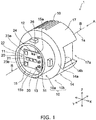
- FIG. 1 is a schematic perspective view illustrating the vehicle lighting device 1 according to the embodiment.
- FIG. 2 is a schematic view of the vehicle lighting device 1 viewed in a direction A in FIG. 1 .
- FIG. 3 is a schematic sectional view of the vehicle lighting device 1 in a direction of line B-B in FIG. 1 .
- an X direction, a Y direction, and a Z direction in each figure indicate three directions orthogonal to each other.
- a direction that is a rightward and leftward direction can be the X direction
- a direction that is a forward and rearward direction can be the Y direction
- a direction that is an upward and downward direction can be the Z direction.
- the vehicle lighting device 1 is provided with a socket 10, a light emitting module 20, and a power supplying portion 30.
- the socket 10 has a storage portion 10a and a heat radiating portion 10b.
- the storage portion 10a has the mounting portion 11, bayonets 12, and the insulating portion 13.
- the mounting portion 11 has a tubular shape.
- the mounting portion 11 can have, for example, a cylindrical shape.
- the mounting portion 11 is provided on a side of a flange 14 opposite to a side in which heat radiating fins 16 are provided.
- the mounting portion 11 surrounds a loading portion 15.
- An external dimension of the mounting portion 11 in a direction (X direction or the Z direction) orthogonal to a center axis 1 a of the vehicle lighting device 1 is smaller than an external dimension of the flange 14.
- the bayonets 12 are provided on a side surface of the mounting portion 11 and protrude to the outside of the vehicle lighting device 1.
- the bayonets 12 face the flange 14.
- a plurality of bayonets 12 are provided.
- the vehicle lighting device 1 When mounting the vehicle lighting device 1 on a housing 101, a portion of the mounting portion 11 in which the bayonets 12 are provided is inserted into an attachment hole 101a provided in the housing 101 (see FIG. 12 ). Then, the vehicle lighting device 1 is held in the housing 101 by rotating the vehicle lighting device 1. That is, the bayonets 12 are provided to be used in twist-lock.
- the insulating portion 13 is provided on an inside of the mounting portion 11.
- the storage portion 10a can be formed by integrally molding the mounting portion 11, the bayonets 12, and the insulating portion 13 or can be formed by joining these members. However, if the mounting portion 11, the bayonets 12, and the insulating portion 13 are integrally molded, it is possible to improve resistance against an external force and achieve reduction in manufacturing cost.
- the storage portion 10a has a function of storing the light emitting module 20 and a function of insulating power supply terminals 31.
- the mounting portion 11, the bayonets 12, and the insulating portions 13 are formed of an insulating material.
- the insulating material can be, for example, an organic material such as resin, an inorganic material such as ceramics (for example, aluminum oxide, aluminum nitride, or the like), or the like.
- the insulating material having high thermal conductivity can be, for example, ceramics (for example, aluminum oxide, aluminum nitride, or the like) and resin having high thermal conductivity. Resin having high thermal conductivity is obtained, for example, by mixing fibers or particles made of aluminum oxide having high thermal conductivity to resin such as polyethylene terephthalate (PET) and nylon.
- PET polyethylene terephthalate
- the mounting portion 11, the bayonets 12, and the insulating portion 13 can be also formed of a conductive material such as metal. However, it is necessary to provide a layer formed of the insulating material between the power supply terminal 31 and the insulating portion 13 or to form only the insulating portion 13 from the insulating material.
- the heat radiating portion 10b has the flange 14, the loading portion 15, the heat radiating fins 16, and a projection portion 17.
- the flange 14 has a plate shape.
- the flange 14 can have, for example, a disk shape.
- a distance between the outside surface of the flange 14 and the center axis 1 a of the vehicle lighting device 1 is longer than a distance between the outside surface of the bayonet 12 and the center axis 1 a of the vehicle lighting device 1. That is, the outside surface of the flange 14 is positioned on the outside of the vehicle lighting device 1 more than the outside surface of the bayonet 12.
- the loading portion 15 can have a cylindrical shape.
- the loading portion 15 is provided on a surface 14a of the flange 14 on a side opposite to the side in which the heat radiating fins 16 are provided.
- a recessed portion 15a is provided on the side surface of the loading portion 15.
- the insulating portion 13 is provided on the inside of the recessed portion 15a.
- the light emitting module 20 (substrate 21) is provided on a surface 15b of the loading portion 15 on a side opposite to the flange 14 side.
- the heat radiating fins 16 are provided on the surface 14b of the flange 14 on a side opposite to the side in which the loading portion 15 is provided.
- a plurality of heat radiating fins 16 can be provided.
- the plurality of heat radiating fins 16 can be provided in parallel to each other.
- the heat radiating fins 16 can have a plate shape.
- the projection portion 17 has a function of protecting an end portion of the power supply terminal 31 and a function of holding a connector 105.
- the projection portion 17 is provided on the surface 14b of the flange 14 in which the heat radiating fins 16 are provided.
- the projection portion 17 can have a block shape.
- a recessed portion 17a is provided on an outside surface of the projection portion 17. The recessed portion 17a is opened on the outside surface of the projection portion 17.
- a hole 17b is provided in the projection portion 17.
- the hole 17b penetrates between an end surface of the projection portion 17 on a side opposite to the flange 14 side and the surface 14a of the flange 14 on a side opposite to the side in which the heat radiating fins 16 are provided.
- the end portion of the power supply terminal 31 protrudes on the flange 14 side of the hole 17b.
- a part of the insulating portion 13 is exposed on the flange 14 side of the hole 17b. That is, an opening of the hole 17b on the flange 14 side is closed by the insulating portion 13.
- the hole 17b is not connected to the recessed portion 17a.
- the connector 105 having a sealing member 105a is inserted into the hole 17b. Therefore, a cross section shape of the hole 17b is fitted to a cross section of the connector 105 having the sealing member 105a.
- a cross section dimension of the hole 17b in a direction orthogonal to the center axis 1a of the vehicle lighting device 1 is slightly smaller than an external shape dimension of the sealing member 105a provided in a body of the connector 105. Therefore, when the connector 105 having the sealing member 105a is inserted into the hole 17b, the hole 17b is sealed to be water tightness.
- the heat radiating portion 10b can be formed by integrally molding the flange 14, the loading portion 15, the heat radiating fins 16, and the projection portion 17 or can be formed by joining these members by individually forming these members. However, if the flange 14, the loading portion 15, the heat radiating fins 16, and the projection portion 17 are integrally molded, it is possible to improve the heat radiation property, to improve resistance against an external force, to achieve reduction in manufacturing cost, and the like.
- the heat radiating portion 10b has a function of loading the light emitting module 20 and a function of discharging heat generated in the light emitting module 20 to the outside.
- the flange 14, the loading portion 15, the heat radiating fins 16, and the projection portion 17 are formed of a material having high thermal conductivity considering the function of discharging heat.
- the material having high thermal conductivity can be metal such as aluminum and aluminum alloy, ceramics such as aluminum oxide and aluminum nitride, resin having high thermal conductivity, or the like.
- the material of the storage portion 10a and the material of the heat radiating portion 10b can be different from each other.
- the storage portion 10a is formed of the insulating material such as resin and the heat radiating portion 10b can be formed of the material having high thermal conductivity such as metal (for example, aluminum alloy and the like).
- the mounting portion 11 is provided on a side of the flange 14 opposite to the side in which the heat radiating fins 16 are provided. I n addition, the mounting portion 11 surrounds the loading portion 15. However, the mounting portion 11 does not surround the flange 14, the heat radiating fins 16, and the projection portion 17.
- the heat radiating portion 10b is joined to the storage portion 10a.
- the insulating portion 13 of the storage portion 10a is inserted into the inside of the recessed portion 15a of the heat radiating portion 10b.
- the loading portion 15 of the heat radiating portion 10b is inserted into the inside of the mounting portion 11 of the storage portion 10a.
- the storage portion 10a and the heat radiating portion 10b may be fitted into each other, or may be joined using adhesive and the like.
- the storage portion 10a and the heat radiating portion 10b may be joined by insert molding, or the storage portion 10a and the heat radiating portion 10b may be joined by heat welding.
- interface is formed between the storage portion 10a and the heat radiating portion 10b. If the interface is formed between the storage portion 10a and the heat radiating portion 10b, there is a concern that moisture enters from the interface. In this case, if the storage portion 10a and the heat radiating portion 10b are bonded and the like, it is possible to suppress entrance of moisture from the interface. However, it is difficult to completely sealing the interface.
- a temperature of environment of use is -40°C to 85°C. Therefore, even if initially it is water tightness, there is a concern that water tightness is lowered together with elapse of time by thermal stress generated by a difference in thermal expansion.
- the position of the end surface 11 a of the mounting portion 11 on the flange 14 side and the position of the end surface 13a of the insulating portion 13 on the flange 14 side are on the light emitting module 20 side more than the position of the surface 14b of the flange 14.
- an external dimension of the mounting portion 11 in a direction orthogonal to the center axis 1 a of the vehicle lighting device 1 is smaller than an external dimension of the flange 14.
- the interface between the mounting portion 11 and the flange 14 can be sealed by a sealing member 104.
- a part of the insulating portion 13 is exposed on the flange 14 side of the hole 17b. That is, the interface between the insulating portion 13 and the flange 14 is exposed on the inside of the hole 17b.
- the connector 105 having the sealing member 105a is inserted into the hole 17b.
- the connector 105 having the sealing member 105a is inserted into the hole 17b, the hole 17b is sealed to be water tightness. As a result, it is possible to suppress that the moisture enters from the interface between the insulating portion 13 and the flange 14.
- the moisture is mainly on the outside of the housing 101 of a vehicle lamp 100. Therefore, moisture entering on the inside of the sealing member 104 from the inside of the housing 101 is little.
- the vehicle lighting device 1 of the embodiment it is possible to suppress that the moisture enters from the interface even if the storage portion 10a and the heat radiating portion 10b are bonded.
- the light emitting module 20 is provided on the surface 15b of the loading portion 15 on the side opposite to the flange 14 side.
- the light emitting module 20 has the substrate 21, a light emitting element 22, a resistor 23a (corresponding to an example of a first resistor), a resistor 23b (corresponding to an example of a second resistor), and a control portion 24.
- the substrate 21 is provided on the surface 15b of the loading portion 15.
- the substrate 21 has a plate shape.
- a wiring pattern 26 is provided on the surface of the substrate 21.
- a material or a structure of the substrate 21 is not particularly limited.
- the substrate 21 can be formed of an inorganic material such as ceramics (for example, aluminum oxide, aluminum nitride, and the like), an organic material such as paper phenol and glass epoxy, and the like.
- the substrate 21 may be obtained by coating a surface of a metal plate with an insulating material.
- the insulating material may be formed of an organic material or may be formed of an inorganic material.
- the substrate 21 is formed by using a material having high thermal conductivity in terms of heat radiation.
- a material having high thermal conductivity ceramics such as aluminum oxide or aluminum nitride, resin having high thermal conductivity, a material that is obtained by coating a surface of a metal plate with an insulating material, and the like can be exemplified.
- the substrate 21 may be a single layer or may be a multi-layer.
- the light emitting element 22 is provided on the substrate 21.
- the light emitting element 22 is electrically connected to the wiring pattern 26 provided on the surface of the substrate 21.
- the light emitting element 22 can be, for example, a light emitting diode, an organic light emitting diode, a laser diode, and the like.
- a form of the light emitting element 22 is not particularly limited.
- the light emitting element 22 can be a light emitting element of a surface mounting type such as Plastic Leaded Chip Carrier (PLCC) type. Moreover, the light emitting element 22 illustrated in FIGS. 1 and 3 is the light emitting element of the surface mounting type.
- PLCC Plastic Leaded Chip Carrier
- the light emitting element 22 can be, for example, a light emitting element having a lead wire of a shell type and the like.
- the light emitting element 22 can be mounted by Chip On Board (COB).
- COB Chip On Board
- the sealing portion can include a phosphor.
- the phosphor can be, for example, a YAG-based phosphor (yttrium-aluminum-garnet based fluorescent material).
- the YAG-based phosphor is excited by blue light emitted from the light emitting element 22 and yellow fluorescence is emitted from the YAG-based phosphor. Then, white light is emitted from the vehicle lighting device 1 by mixing blue light and yellow light.
- types of the phosphors and types of the light emitting elements 22 are not limited to the examples described above. The types of the phosphors and the types of the light emitting elements 22 can be appropriately changed such that a desired emitting color is obtained in accordance with the application of the vehicle lighting device 1 and the like.
- a light emitting surface of the light emitting element 22 faces a front side of the vehicle lighting device 1.
- the light emitting element 22 mainly emits light on the front side of the vehicle lighting device 1.
- the number, sizes, and arrangements of the light emitting elements 22 are not limited to the examples described above, and can be appropriately changed in accordance with the size and the application of the vehicle lighting device 1, and the like.
- a plurality of light emitting elements 22 are provided side by side in a row in the X direction.
- the X direction is the direction that is the horizontal direction when attaching the vehicle lighting device 1 to the vehicle lamp 100.
- the Z direction is the direction that is the vertical direction when attaching the vehicle lighting device 1 to the vehicle lamp 100.
- a dimension of the row of the light emitting elements 22 in the X direction is longer than a dimension of the row of the light emitting elements 22 in the Z direction.
- the vehicle lighting device 1 can have the light distribution characteristics for vehicle which are wide in the horizontal direction and are narrow in the vertical direction.
- the resistors 23a and 23b are provided on the substrate 21.
- the resistors 23a and 23b are electrically connected to the wiring pattern 26 provided on the surface of the substrate 21.
- the resistors 23a and 23b controls a current flowing through the light emitting element 22.
- a value of the current flowing through the light emitting element 22 is made to fall within a predetermined range by the resistors 23a and 23b so that the brightness of the light emitting element 22 falls within a predetermined range.
- a value of the current flowing through the light emitting element 22 can be within a predetermined range by changing resistance values of the resistors 23a and 23b.
- the resistors 23a and 23b can be, for example, resistors of a surface mounting type, resistors (metal oxide film resistor) having a lead wire, film-like resistors formed using a screen printing method, and the like. Moreover, the resistors 23a and 23b illustrated in FIGS. 1 and 3 are the film-like resistors.
- the number, sizes, and arrangements of the resistors 23a and 23b are not limited to the examples described above, and can be appropriately changed in accordance with the number and a specification of the light emitting element 22, and the like.
- the control portion 24 is provided on the substrate 21.
- the control portion 24 is electrically connected to the wiring pattern 26 provided on the surface of the substrate 21. Moreover, details regarding connection between the light emitting element 22, the resistors 23a and 23b, the control portion 24, and the like will be described later (see FIG. 6A and the like).
- diodes it is possible to provide diodes to prevent a reverse voltage from being applied to the light emitting element 22 and to prevent pulse noise from a reverse direction from being applied to the light emitting element 22.
- a pull-down resistor to detect disconnection of the light emitting element 22, to prevent erroneous lighting, and the like.
- a cover portion for covering the wiring pattern 26, the film-like resistor, and the like can include, for example, a glass material.
- the power supplying portion 30 has a plurality of power supply terminals 31.
- the plurality of power supply terminals 31 are provided on the inside of the socket 10 (insulating portion 13).
- the plurality of power supply terminals 31 extend on the inside of the insulating portion 13.
- One-side end portion of the plurality of power supply terminals 31 protrudes from an end surface of the insulating portion 13 on a side opposite to the flange 14 side and is electrically connected to the wiring pattern 26 provided in the substrate 21.
- the other end portion of the plurality of power supply terminals 31 protrudes from the end surface 13a of the insulating portion 13 on the flange 14 side.
- the other end portion of the plurality of power supply terminals 31 is exposed on the inside of the hole 17b.
- the number and a shape of the power supply terminals 31, and the like are not limited to the examples described above, and can be appropriately changed.
- the power supplying portion 30 can include a substrate (not illustrated), circuit components (for example, integrated circuit, capacitors, and the like), and the like.
- the substrate (not illustrated), the circuit components, and the like can be provided on the inside of the storage portion 10a, the inside of the heat radiating portion 10b, and the like.
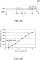
- FIG. 4A is a circuit diagram illustrating the light emitting module 200 according to the comparison example.
- FIG. 4B is a graph illustrating a relationship between an input voltage and a total luminous flux in the light emitting module 200.
- the light emitting module 200 is provided with light emitting elements 22 and a resistor 23a. Similar to the light emitting module 20 described above, the light emitting elements 22 and the resistor 23a are electrically connected to a wiring pattern 26 provided on a surface of a substrate 21. However, the light emitting module 200 is not provided with a control portion 24.
- a battery is power supply, but a voltage applied to the vehicle lighting device 1 fluctuates.
- an operation standard voltage (rated voltage) of the vehicle lighting device 1 for a general automobile is approximately 13.5 V.
- the voltage applied to the vehicle lighting device 1 fluctuates due to a voltage drop of the battery, an operation of an alternator, an influence of a circuit, and the like.
- an operating voltage range (voltage fluctuation range) is determined.
- the operating voltage range is generally equal to or greater than 9 V and equal to or less than 16 V, and may also be equal to or greater than 7 V and equal to or less than 16 V in some case.
- the light emitting element 22 has a voltage drop in a forward direction. Therefore, as illustrated in FIG. 4B , when the input voltage (applied voltage) of the plurality of light emitting elements 22 which are connected in series decreases, an amount of light emitted from the plurality of light emitting elements 22 decreases. Therefore, in the vicinity of a lower limit of the operating voltage range, there is a concern that the total luminous flux of the vehicle lighting device 1 is less than a specified value.
- the voltage drop of the light emitting elements 22 in the forward direction is approximately 3 V
- the voltage drop of 9 V generates.
- the resistor 23a is connected in series to the three light emitting elements 22. Therefore, when the input voltage is approximately 9 V, almost no current flows through the three light emitting elements 22 and the total luminous flux of the vehicle lighting device 1 is less than the specified value.
- FIG. 5A is a circuit diagram illustrating a light emitting module 210 according to a comparison example.
- FIG. 5B is a graph illustrating a relationship between an input voltage and a total luminous flux in the light emitting module 210.
- the light emitting module 210 is provided with the light emitting elements 22, a resistor 23a, a voltmeter 211, and a switch 212.
- the voltmeter 211 is connected in parallel to the resistor 23a.
- the voltmeter 211 measures the input voltage.
- the three light emitting elements 22 are electrically connected in series to the resistor 23a.
- the switch 212 is connected in parallel to one light emitting element 22 farthest from the inside side.
- the switch 212 is opened. Then, a current Ia flows through the three light emitting elements 22 connected in series to each other and light is emitted from the three light emitting elements 22.
- the switch 212 is closed. Then, a current Ib flows through the two light emitting elements 22 connected in series to each other and almost no current flows through the light emitting elements 22 connected in parallel to the switch 212. Therefore, the current flowing through two light emitting elements 22 can be increased. As a result, it is possible to suppress the total luminous flux of the vehicle lighting device 1 is less than the specified value in the vicinity of a lower limit of operating voltage range.
- FIG. 6A is a circuit diagram illustrating a light emitting module 20 according to an embodiment.
- FIG. 6B is a graph illustrating a relationship between an input voltage and a total luminous flux in the light emitting module 20.
- the light emitting module 20 has a first circuit portion 20a, a second circuit portion 20b, and a third circuit portion 20c.
- the first circuit portion 20a has at least one light emitting element 22 and a resistor 23a connected in series to the light emitting element 22. Moreover, in a case where a plurality of light emitting elements 22 are provided, the plurality of light emitting elements 22 and the resistor 23a are connected in series.
- the second circuit portion 20b is connected in parallel to the first circuit portion 20a.
- the second circuit portion 20b has at least a control portion 24. Moreover, in a case where the control portion 24 and a resistor 23b are provided, the control portion 24 and the resistor 23b are connected in series.
- the third circuit portion 20c is connected in series to the first circuit portion 20a and the second circuit portion 20b.
- the third circuit portion 20c has at least one light emitting element 22. Moreover, in a case where a plurality of light emitting elements 22 are provided, the plurality of light emitting elements 22 are connected in series.
- the control portion 24 measures an input voltage and in a case where the measured input voltage is a predetermined value, a current I2 flows through the second circuit portion 20b.
- the control portion 24 has a function of measuring the input voltage and a function of switch for switching ON and OFF of the current I2.
- the control portion 24 can perform the measurement of the input voltage by providing an input voltage determination circuit using a Zener diode (constant voltage diode), a comparator using an operational amplifier, or the like.
- the control portion 24 prevents the current I2 from flowing through the second circuit portion 20b.
- the control portion 24 causes the built-in switching transistor to be in an OFF state. Then, the current I1 flows through all the light emitting elements 22 connected in series and light is emitted from all the light emitting elements 22.
- the control portion 24 causes the current 12 to flow through the second circuit portion 20b.
- the control portion 24 causes the built-in switching transistor to be in an ON state.
- a current that is obtained by adding the current 11 from the first circuit portion 20a to the current I2 from the second circuit portion 20b flows through the plurality of light emitting elements 22 provided in the third circuit portion 20c.
- the current I1 flows through the light emitting element 22 provided in the first circuit portion 20a.
- the vehicle lighting device 1 of the embodiment even in a case where a voltage applied to the vehicle lighting device 1 decreases, it is possible to secure a required total luminous flux and to suppress fluctuation of the total luminous flux.
- the resistor 23b is the film-like resistor.
- the adjustment of the resistance value can be performed as follows. First, the film-like resistor (resistor 23b) is formed on a surface of a substrate 21 using screen printing method or the like. Next, a part of the resistor 23b is removed by irradiating the resistor 23b with laser light. Then, the resistance value of the resistor 23b is changed by a size of a removed portion or the like. In this case, if a part of the resistor 23b is removed, the resistance value increases.
- FIG. 7 is a circuit diagram illustrating a light emitting module 20 according to another embodiment.
- the light emitting module 20 has a first circuit portion 20a, a second circuit portion 20b, and a third circuit portion 20c.
- the first circuit portion 20a may have at least one light emitting element 22 and a resistor 23a that is connected in series to the light emitting element 22.
- the first circuit portion 20a has one light emitting element 22 and the resistor 23a connected in series to the light emitting element 22.
- the first circuit portion 20a has two light emitting elements 22 connected in series and the resistor 23a.
- the third circuit portion 20c may have at least one light emitting element 22.
- the third circuit portion 20c has the two light emitting elements 22 connected in series.
- the third circuit portion 20c has one light emitting element 22.
- the voltage value that is the determination reference can be reduced. Therefore, it is possible to reduce the number of times of flowing of the current I2 through the second circuit portion 20b. As a result, since the number of times of increasing the total luminous flux can be reduced, it is possible to suppress occurrence of the feeling of strangeness.
- FIG. 8 is a circuit diagram illustrating a light emitting module 20 according to another embodiment.
- the light emitting module 20 has a first circuit portion 20a, a second circuit portion 20b, a third circuit portion 20c, and a resistor 23b (corresponding to an example of a third resistor).
- the second circuit portion 20b is connected in parallel to the first circuit portion 20a.
- the third circuit portion 20c is connected in series to the first circuit portion 20a and the second circuit portion 20b.
- the resistor 23b is connected in series to the first circuit portion 20a and the second circuit portion 20b.
- the second circuit portion 20b may have at least a control portion 24.
- the second circuit portion 20b has the control portion 24 and the resistor 23b connected in series.
- the second circuit portion 20b has the control portion 24.
- the resistor 23a and the resistor 23b cooperate to control the current I1 flowing through all the light emitting elements 22.
- the resistor 23b controls the current I2 flowing through the light emitting elements 22 provided in the third circuit portion 20c.
- the effect described above can also be enjoyed by the embodiment. That is, even in a case where the voltage applied to the vehicle lighting device 1 decreases, it is possible to secure the required total luminous flux and to suppress fluctuation of the total luminous flux.
- FIG. 9A is a circuit diagram illustrating a light emitting module 20 according to another embodiment.
- FIG. 9B is a graph illustrating a relationship between an input voltage and a total luminous flux in the light emitting module 20.
- the light emitting module 20 has a first circuit portion 20a, a second circuit portion 20b, and a third circuit portion 20c.
- the second circuit portion 20b may have at least a control portion 24.
- the second circuit portion 20b has the control portion 24 and the resistor 23b connected in series.
- the second circuit portion 20b has a control portion 24 and a constant current circuit 23b1 connected in series. That is, in the embodiment, the second circuit portion 20b has the constant current circuit 23b1 instead of a resistor 23b.
- the constant current circuit 23b1 can be, for example, a constant current circuit using a constant current diode, a current limiter circuit using a transistor, a constant current IC, or the like.
- a value of the current I2 flowing through the second circuit portion 20b can be constant by the constant current circuit 23b1. Therefore, as illustrated in FIG. 9B , it is possible to suppress an increase in the total luminous flux of the vehicle lighting device 1 in the vicinity of the lower lim it of operating voltage range.
- FIGS. 10A and 10B are circuit diagrams illustrating a light emitting module 20 according to another embodiment.
- the light emitting module 20 has a first circuit portion 20a, a second circuit portion 20ba, and a third circuit portion 20c.
- the second circuit portion 20ba has a control portion 24a and a resistor 23b connected in series to the control portion 24a.
- the control portion 24a is connected in parallel to a resistor 23a.
- the control portion 24 described above has the function of measuring the input voltage and the function of the switch for switching ON and OFF of the current I2.
- the control portion 24a has a function of measuring the input voltage, a function of a switch for switching ON and OFF of the current I2, and a function of a switch for switching ON and OFF of a current I1. That is, the control portion 24a further has the function of the switch for switching ON and OFF of the current I1.
- the control portion 24a can have switching transistors for switching ON and OFF of the current I1 and the current I2, and the like.
- the function of measuring the input voltage can be, for example, similar to the control portion 24.
- a resistance value of the resistor 23a is adjusted so that a value A of the current I1 (value A of the current I1 flowing through the resistor 23a) flowing through the light emitting elements 22 provided in the first circuit portion 20a and the third circuit portion 20c is within a predetermined range.
- the resistance value of the resistor 23b is adjusted so that a value B (value B of the current I2 flowing through the resistor 23b) of the current I2 flowing through the light emitting elements 22 provided in the third circuit portion 20c is within a predetermined range.
- the resistance value of the resistor 23b is adjusted so that the value B of the current I2 satisfies the following expression (1).
- A is a value of the current I1 flowing through the resistor 23a
- B is a value of current flowing through the resistor 23b
- Na is the number of the light emitting elements 22 provided in the first circuit portion 20a and the third circuit portion 20c
- Nb is the number of the light emitting elements 22 provided in the third circuit portion 20c.
- the resistance value of the resistor 23b is adjusted so that the value B of the current I2 becomes 142.5 mA (milliamperes) ⁇ B ⁇ 157.5 mA (milliamperes).
- control portion 24a measures the input voltage.
- the control portion 24a causes the current I2 to flow through the second circuit portion 20ba.
- the control portion 24a prevents the current I2 from flowing through the second circuit portion 20ba by a built-in switching transistor.
- control portion 24a causes the current I1 to flow through the first circuit portion 20a and the third circuit portion 20c.
- the control portion 24a causes the current I1 to flow through the first circuit portion 20a and the third circuit portion 20c by the built-in switching transistor.
- the current I1 flows through all the light emitting elements 22 connected in series and light is emitted from all the light emitting elements 22.
- the control portion 24a prevents the current I1 from flowing through the light emitting element 22 provided in the first circuit portion 20a.
- the control portion 24a prevents the current 11 from flowing through the light emitting element 22 provided in the first circuit portion 20a by the built-in switching transistor.
- control portion 24a causes the current I2 to flow through the second circuit portion 20ba.
- control portion 24a causes the current I2 to flow through the second circuit portion 20ba by the built-in switching transistor.
- the current I2 from the second circuit portion 20ba flows through only the light emitting elements 22 provided in the third circuit portion 20c.
- the luminous flux of light emitted from the light emitting elements 22 is substantially proportional to the value of the current flowing through the light emitting element 22.
- the total luminous flux in a case where the current 11 flows through all the light emitting elements 22 provided in the first circuit portion 20a and the third circuit portion 20c, and the total luminous flux in a case where the current 12 flows through the light emitting elements 22 provided in the third circuit portion 20c can be substantially equal to each other as seen with a naked eye during switching when the input voltage is a predetermined value.
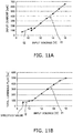
- FIG. 11A is a graph illustrating a relationship between an input voltage and an input current in the light emitting module 20.
- FIG. 11B is a graph illustrating a relationship between the input voltage and the total luminous flux in the light emitting module 20.
- the value B of the current I2 satisfies the expression (1).
- the total luminous flux in a case where the current I1 flows through all the light emitting elements 22 provided in the first circuit portion 20a and the third circuit portion 20c, and the total luminous flux in a case where the current I2 flows through only the light emitting elements 22 provided in the third circuit portion 20c can be substantially equal to each other.
- the vehicle lamp 100 is exemplified.
- the vehicle lamp 100 is not limited to the front combination light provided in the automobile.
- the vehicle lamp 100 may be a vehicle lamp provided in an automobile, a railway vehicle, and the like.
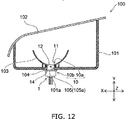
- FIG. 12 is a partial sectional view schematically illustrating the vehicle lamp 100.
- the vehicle lighting device 1 As illustrated in FIG. 12 , the vehicle lighting device 1, the housing 101, a cover 102, an optical element portion 103, the sealing member 104, and the connector 105 are provided in the vehicle lamp 100.
- the housing 101 has a box shape of which one end portion is opened.
- the housing 101 can be formed of, for example, resin and the like through which light is not transmitted.
- the attachment hole 101a into which a portion of the mounting portion 11 in which the bayonets 12 are provided is inserted is provided in a bottom surface of the housing 101. Recessed portions into which the bayonets 12 provided in the mounting portion 11 are inserted are provided in a periphery of the attachment hole 101 a.
- an attaching member having the attachment hole 101a may be provided in the housing 101.
- the vehicle lighting device 1 When attaching the vehicle lighting device 1 to the vehicle lamp 100, the vehicle lighting device 1 is attached in the direction illustrated in FIG. 1 .
- the plurality of light emitting elements 22 are provided side by side in a row in the X direction (horizontal direction). Therefore, it is possible to obtain the light distribution characteristics for vehicle which are wide in the horizontal direction and are narrow in the vertical direction.
- the plurality of power supply terminals 31 are provided side by side in a row in the Z direction (vertical direction).
- the plurality of heat radiating fins 16 are provided side by side in a row in the X direction (horizontal direction).
- the heat radiating fins 16 have the shape extending straightly in the Z direction (vertical direction). Therefore, the flow of a rising air flow 300 in the region in which the plurality of heat radiating fins 16 are provided can be prevented from being hindered by the projection portion 17, the connector 105, and the heat radiating fins 16.
- the vehicle lighting device 1 has the light distribution characteristics for vehicle which are wide in the horizontal direction and are narrow in the vertical direction, and it is possible to improve the heat radiation.
- the cover 102 is provided so as to close an opening of the housing 101.
- the cover 102 can be formed of resin and the like having a light-transmitting property.
- the cover 102 can have functions of a lens and the like.
- the optical element portion 103 performs reflection, diffusion, guiding, and condensing of the light emitted from the vehicle lighting device 1, formation of a predetermined light distribution pattern, and the like.
- the optical element portion 103 illustrated in FIG. 12 is a reflector.
- the optical element portion 103 reflects the light emitted from the vehicle lighting device 1, and causes the predetermined light distribution pattern to be formed.
- the optical element portion 103 is the reflector, the optical element portion 103 can be provided on the inside of the housing 101 so as to be coaxially with the center axis of the attachment hole 101a.
- the sealing member 104 is provided between the flange 14 and the housing 101.
- the sealing member 104 can have an annular shape.
- the sealing member 104 can be formed of a material having elasticity such as rubber or silicone resin.
- the sealing member 104 When attaching the vehicle lighting device 1 to the vehicle lamp 100, the sealing member 104 is interposed between the flange 14 and the housing 101. Thus, an inside space of the housing 101 is sealed by the sealing member 104. In addition, as described above, the interface between the mounting portion 11 and the flange 14 is sealed by the sealing member 104. In addition, the bayonets 12 are pressed against the housing 101 by elastic force of the sealing member 104. Thus, the vehicle lighting device 1 can be suppressed to be separated from the housing 101.
- the connectors 105 are fitted into end portions of the plurality of power supply terminals 31 exposed on the inside of the hole 17b. Power supply (not illustrated) and the like are electrically connected to the connectors 105. Therefore, power supply (not illustrated) and the like are electrically connected to the light emitting elements 22 by fitting the connectors 105 into the end portions of the power supply terminals 31.
- the connectors 105 have stepped portions. Then, the sealing member 105a is attached to the stepped portions (see FIG. 3 ). The sealing member 105a is provided to prevent entrance of water on the inside of the hole 17b. When the connector 105 having the sealing member 105a is inserted into the hole 17b, the hole 17b is sealed to be water tightness.
- the sealing member 105a can have an annular shape.
- the sealing member 105a can be formed of a material having elasticity such as rubber or silicone resin.
- the connector 105 can also be joined, for example, to an element on the socket 10 side using adhesive or the like.
Landscapes
- Lighting Device Outwards From Vehicle And Optical Signal (AREA)
Abstract
Description
- Embodiments described herein relate generally to a vehicle lighting device and a vehicle lamp.
- There is a vehicle lighting device including a plurality of light emitting diodes (LEDs) which are connected in series.
- Here, a voltage applied to the vehicle lighting device fluctuates. Therefore, in the vehicle lighting device, an operating voltage range (voltage fluctuation range) is determ ined.
- In addition, the light emitting diode has a forward voltage drop. Therefore, when the voltage applied to the plurality of light emitting diodes connected in series decreases, an amount of light emitted from the plurality of light emitting diodes decreases and there is a concern that a total luminous flux of the vehicle lighting device becomes less than a specified value.
- Therefore, a technique is proposed in which in a case where the voltage applied to the vehicle lighting device decreases, a current does not flow through some light emitting diodes among the plurality of light emitting diodes which are connected in series.
- Thus, even in a case where the voltage applied to the vehicle lighting device decreases, it is possible to secure a required total luminous flux.
- However, when the current does not flow through some light emitting diodes, there is a new problem that the current flowing through remaining light emitting diodes suddenly increases and the total luminous flux rapidly increases.
- Therefore, it is desired to develop a technique in which even in a case where the voltage applied to the vehicle lighting device decreases, it is possible to secure a required total luminous flux and to suppress fluctuation of a total luminous flux.
-
-
FIG. 1 is a schematic perspective view illustrating thevehicle lighting device 1 according to an embodiment. -
FIG. 2 is a schematic view of thevehicle lighting device 1 viewed in a direction A inFIG. 1 . -
FIG. 3 is a schematic sectional view of thevehicle lighting device 1 in a direction of line B-B inFIG. 1 . -
FIG. 4A is a circuit diagram illustrating alight emitting module 200 according to a comparison example.FIG. 4B is a graph illustrating a relationship between an input voltage and a total luminous flux in thelight emitting module 200. -
FIG. 5A is a circuit diagram illustrating alight emitting module 210 according to a comparison example.FIG. 5B is a graph illustrating a relationship between an input voltage and a total luminous flux in thelight emitting module 210. -
FIG. 6A is a circuit diagram illustrating alight emitting module 20 according to an embodiment.FIG. 6B is a graph illustrating a relationship between an input voltage and a total luminous flux in thelight emitting module 20. -
FIG. 7 is a circuit diagram illustrating alight emitting module 20 according to another embodiment. -
FIG. 8 is a circuit diagram illustrating alight emitting module 20 according to still another embodiment. -
FIG. 9A is a circuit diagram illustrating alight emitting module 20 according to still another embodiment.FIG. 9B is a graph illustrating a relationship between an input voltage and a total luminous flux in thelight emitting module 20. -
FIGS. 10A and 10B are circuit diagrams illustrating alight emitting module 20 according to still another embodiment. -
FIG. 11A is a graph illustrating a relationship between an input voltage and an input current in thelight emitting module 20.FIG. 11B is a graph illustrating a relationship between the input voltage and a total luminous flux in thelight emitting module 20. -
FIG. 12 is a partial sectional view schematically illustrating thevehicle lamp 100. - In general, according to one embodiment, a vehicle lighting device includes a first circuit portion that has at least one light emitting element and a first resistor connected in series to the light emitting element; a second circuit portion that is connected in parallel to the first circuit portion and has at least a control portion; a third circuit portion that is connected in series to the first circuit portion and the second circuit portion, and has at least one light emitting element. The control portion measures the input voltage and causes a current to flow through the third circuit portion in a case where the measured input voltage is a predetermined value.
- According to the vehicle lighting device, even in a case where a voltage applied to the vehicle lighting device decreases, it is possible to secure a required total luminous flux and to suppress fluctuation of the total luminous flux.
- Hereinafter, exemplary embodiments will be described with reference to the drawings. Moreover, the same reference numerals are given to the same configuration elements in each drawing and detailed description will be appropriately omitted.
- A
vehicle lighting device 1 of the exemplary embodiment, for example, can be provided in automobiles, railway vehicles, or the like. As thevehicle lighting device 1 provided in the automobile, for example, a front combination light (formed by appropriately combining, for example, a daytime running lamp (DRL), a position lamp, a turn signal lamp, and the like), a rear combination light (formed by appropriately combining, for example, a stop lamp, a tail lamp, a turn signal lamp, a back lamp, a fog lamp, and the like), and the like can be exemplified. However, application of thevehicle lighting device 1 is not limited to the examples. -
FIG. 1 is a schematic perspective view illustrating thevehicle lighting device 1 according to the embodiment. -
FIG. 2 is a schematic view of thevehicle lighting device 1 viewed in a direction A inFIG. 1 . -
FIG. 3 is a schematic sectional view of thevehicle lighting device 1 in a direction of line B-B inFIG. 1 . - Moreover, an X direction, a Y direction, and a Z direction in each figure indicate three directions orthogonal to each other. For example, when attaching the
vehicle lighting device 1 to avehicle lamp 100, a direction that is a rightward and leftward direction (horizontal direction) can be the X direction, a direction that is a forward and rearward direction (horizontal direction) can be the Y direction, and a direction that is an upward and downward direction (vertical direction) can be the Z direction. - As illustrated in FI GS. 1, 2, and 3, the
vehicle lighting device 1 is provided with asocket 10, alight emitting module 20, and apower supplying portion 30. - The
socket 10 has astorage portion 10a and aheat radiating portion 10b. - The
storage portion 10a has themounting portion 11,bayonets 12, and theinsulating portion 13. - The
mounting portion 11 has a tubular shape. Themounting portion 11 can have, for example, a cylindrical shape. Themounting portion 11 is provided on a side of aflange 14 opposite to a side in whichheat radiating fins 16 are provided. Themounting portion 11 surrounds aloading portion 15. An external dimension of themounting portion 11 in a direction (X direction or the Z direction) orthogonal to acenter axis 1 a of thevehicle lighting device 1 is smaller than an external dimension of theflange 14. - The
bayonets 12 are provided on a side surface of themounting portion 11 and protrude to the outside of thevehicle lighting device 1. Thebayonets 12 face theflange 14. A plurality ofbayonets 12 are provided. - When mounting the
vehicle lighting device 1 on ahousing 101, a portion of the mountingportion 11 in which thebayonets 12 are provided is inserted into anattachment hole 101a provided in the housing 101 (seeFIG. 12 ). Then, thevehicle lighting device 1 is held in thehousing 101 by rotating thevehicle lighting device 1. That is, thebayonets 12 are provided to be used in twist-lock. - The insulating
portion 13 is provided on an inside of the mountingportion 11. - The
storage portion 10a can be formed by integrally molding the mountingportion 11, thebayonets 12, and the insulatingportion 13 or can be formed by joining these members. However, if the mountingportion 11, thebayonets 12, and the insulatingportion 13 are integrally molded, it is possible to improve resistance against an external force and achieve reduction in manufacturing cost. - The
storage portion 10a has a function of storing thelight emitting module 20 and a function of insulatingpower supply terminals 31. - Therefore, it is preferable that the mounting
portion 11, thebayonets 12, and the insulatingportions 13 are formed of an insulating material. The insulating material can be, for example, an organic material such as resin, an inorganic material such as ceramics (for example, aluminum oxide, aluminum nitride, or the like), or the like. - In this case, it is also possible to form the mounting
portion 11, thebayonets 12, and the insulatingportion 13 from the insulating material having high thermal conductivity considering that heat generated in thelight emitting module 20 is transmitted to the outside. The insulating material having high thermal conductivity can be, for example, ceramics (for example, aluminum oxide, aluminum nitride, or the like) and resin having high thermal conductivity. Resin having high thermal conductivity is obtained, for example, by mixing fibers or particles made of aluminum oxide having high thermal conductivity to resin such as polyethylene terephthalate (PET) and nylon. - Moreover, the mounting
portion 11, thebayonets 12, and the insulatingportion 13 can be also formed of a conductive material such as metal. However, it is necessary to provide a layer formed of the insulating material between thepower supply terminal 31 and the insulatingportion 13 or to form only the insulatingportion 13 from the insulating material. - The
heat radiating portion 10b has theflange 14, theloading portion 15, theheat radiating fins 16, and aprojection portion 17. - The
flange 14 has a plate shape. Theflange 14 can have, for example, a disk shape. A distance between the outside surface of theflange 14 and thecenter axis 1 a of thevehicle lighting device 1 is longer than a distance between the outside surface of thebayonet 12 and thecenter axis 1 a of thevehicle lighting device 1. That is, the outside surface of theflange 14 is positioned on the outside of thevehicle lighting device 1 more than the outside surface of thebayonet 12. - The
loading portion 15 can have a cylindrical shape. Theloading portion 15 is provided on asurface 14a of theflange 14 on a side opposite to the side in which theheat radiating fins 16 are provided. A recessedportion 15a is provided on the side surface of theloading portion 15. The insulatingportion 13 is provided on the inside of the recessedportion 15a. The light emitting module 20 (substrate 21) is provided on asurface 15b of theloading portion 15 on a side opposite to theflange 14 side. - The
heat radiating fins 16 are provided on thesurface 14b of theflange 14 on a side opposite to the side in which theloading portion 15 is provided. A plurality ofheat radiating fins 16 can be provided. The plurality ofheat radiating fins 16 can be provided in parallel to each other. Theheat radiating fins 16 can have a plate shape. - The
projection portion 17 has a function of protecting an end portion of thepower supply terminal 31 and a function of holding aconnector 105. Theprojection portion 17 is provided on thesurface 14b of theflange 14 in which theheat radiating fins 16 are provided. Theprojection portion 17 can have a block shape. A recessedportion 17a is provided on an outside surface of theprojection portion 17. The recessedportion 17a is opened on the outside surface of theprojection portion 17. - A
hole 17b is provided in theprojection portion 17. Thehole 17b penetrates between an end surface of theprojection portion 17 on a side opposite to theflange 14 side and thesurface 14a of theflange 14 on a side opposite to the side in which theheat radiating fins 16 are provided. The end portion of thepower supply terminal 31 protrudes on theflange 14 side of thehole 17b. A part of the insulatingportion 13 is exposed on theflange 14 side of thehole 17b. That is, an opening of thehole 17b on theflange 14 side is closed by the insulatingportion 13. Thehole 17b is not connected to the recessedportion 17a. - The
connector 105 having a sealingmember 105a is inserted into thehole 17b. Therefore, a cross section shape of thehole 17b is fitted to a cross section of theconnector 105 having the sealingmember 105a. - In addition, a cross section dimension of the
hole 17b in a direction orthogonal to thecenter axis 1a of thevehicle lighting device 1 is slightly smaller than an external shape dimension of the sealingmember 105a provided in a body of theconnector 105. Therefore, when theconnector 105 having the sealingmember 105a is inserted into thehole 17b, thehole 17b is sealed to be water tightness. - The
heat radiating portion 10b can be formed by integrally molding theflange 14, theloading portion 15, theheat radiating fins 16, and theprojection portion 17 or can be formed by joining these members by individually forming these members. However, if theflange 14, theloading portion 15, theheat radiating fins 16, and theprojection portion 17 are integrally molded, it is possible to improve the heat radiation property, to improve resistance against an external force, to achieve reduction in manufacturing cost, and the like. - The
heat radiating portion 10b has a function of loading thelight emitting module 20 and a function of discharging heat generated in thelight emitting module 20 to the outside. - Therefore, it is preferable that the
flange 14, theloading portion 15, theheat radiating fins 16, and theprojection portion 17 are formed of a material having high thermal conductivity considering the function of discharging heat. The material having high thermal conductivity can be metal such as aluminum and aluminum alloy, ceramics such as aluminum oxide and aluminum nitride, resin having high thermal conductivity, or the like. - In this case, the material of the
storage portion 10a and the material of theheat radiating portion 10b can be different from each other. For example, thestorage portion 10a is formed of the insulating material such as resin and theheat radiating portion 10b can be formed of the material having high thermal conductivity such as metal (for example, aluminum alloy and the like). - Here, the mounting
portion 11 is provided on a side of theflange 14 opposite to the side in which theheat radiating fins 16 are provided. I n addition, the mountingportion 11 surrounds theloading portion 15. However, the mountingportion 11 does not surround theflange 14, theheat radiating fins 16, and theprojection portion 17. - Therefore, it is possible to efficiently discharge heat generated in the
light emitting module 20 to the outside via theflange 14, theheat radiating fins 16, and theprojection portion 17 which are formed of a material having high thermal conductivity. That is, it is possible to improve the heat radiation property of thevehicle lighting device 1. - I n addition, the
heat radiating portion 10b is joined to thestorage portion 10a. I n this case, the insulatingportion 13 of thestorage portion 10a is inserted into the inside of the recessedportion 15a of theheat radiating portion 10b. Theloading portion 15 of theheat radiating portion 10b is inserted into the inside of the mountingportion 11 of thestorage portion 10a. - The
storage portion 10a and theheat radiating portion 10b may be fitted into each other, or may be joined using adhesive and the like. Thestorage portion 10a and theheat radiating portion 10b may be joined by insert molding, or thestorage portion 10a and theheat radiating portion 10b may be joined by heat welding. - Here, if the
storage portion 10a and theheat radiating portion 10b are bonded, interface is formed between thestorage portion 10a and theheat radiating portion 10b. If the interface is formed between thestorage portion 10a and theheat radiating portion 10b, there is a concern that moisture enters from the interface. In this case, if thestorage portion 10a and theheat radiating portion 10b are bonded and the like, it is possible to suppress entrance of moisture from the interface. However, it is difficult to completely sealing the interface. - In addition, in a case of the
vehicle lighting device 1 provided in the automobile, a temperature of environment of use is -40°C to 85°C. Therefore, even if initially it is water tightness, there is a concern that water tightness is lowered together with elapse of time by thermal stress generated by a difference in thermal expansion. - Thus, in the embodiment, the position of the
end surface 11 a of the mountingportion 11 on theflange 14 side and the position of theend surface 13a of the insulatingportion 13 on theflange 14 side are on thelight emitting module 20 side more than the position of thesurface 14b of theflange 14. - In addition, an external dimension of the mounting
portion 11 in a direction orthogonal to thecenter axis 1 a of thevehicle lighting device 1 is smaller than an external dimension of theflange 14. - Therefore, as illustrated in
FIG. 3 , the interface between the mountingportion 11 and theflange 14 can be sealed by a sealingmember 104. - Moreover, a part of the insulating
portion 13 is exposed on theflange 14 side of thehole 17b. That is, the interface between the insulatingportion 13 and theflange 14 is exposed on the inside of thehole 17b. However, theconnector 105 having the sealingmember 105a is inserted into thehole 17b. - Therefore, when the
connector 105 having the sealingmember 105a is inserted into thehole 17b, thehole 17b is sealed to be water tightness. As a result, it is possible to suppress that the moisture enters from the interface between the insulatingportion 13 and theflange 14. - Moreover, the moisture is mainly on the outside of the
housing 101 of avehicle lamp 100. Therefore, moisture entering on the inside of the sealingmember 104 from the inside of thehousing 101 is little. - As described above, according to the
vehicle lighting device 1 of the embodiment, it is possible to suppress that the moisture enters from the interface even if thestorage portion 10a and theheat radiating portion 10b are bonded. - As illustrated in
FIGS. 1 and3 , thelight emitting module 20 is provided on thesurface 15b of theloading portion 15 on the side opposite to theflange 14 side. - The
light emitting module 20 has thesubstrate 21, alight emitting element 22, aresistor 23a (corresponding to an example of a first resistor), aresistor 23b (corresponding to an example of a second resistor), and acontrol portion 24. - The
substrate 21 is provided on thesurface 15b of theloading portion 15. Thesubstrate 21 has a plate shape. Awiring pattern 26 is provided on the surface of thesubstrate 21. - A material or a structure of the
substrate 21 is not particularly limited. For example, thesubstrate 21 can be formed of an inorganic material such as ceramics (for example, aluminum oxide, aluminum nitride, and the like), an organic material such as paper phenol and glass epoxy, and the like. In addition, thesubstrate 21 may be obtained by coating a surface of a metal plate with an insulating material. Moreover, in a case where the surface of the metal plate is coated with the insulating material, the insulating material may be formed of an organic material or may be formed of an inorganic material. - I n a case where a heating value of the
light emitting element 22 is large, it is preferable that thesubstrate 21 is formed by using a material having high thermal conductivity in terms of heat radiation. As the material having high thermal conductivity, ceramics such as aluminum oxide or aluminum nitride, resin having high thermal conductivity, a material that is obtained by coating a surface of a metal plate with an insulating material, and the like can be exemplified. - In addition, the
substrate 21 may be a single layer or may be a multi-layer. - The
light emitting element 22 is provided on thesubstrate 21. Thelight emitting element 22 is electrically connected to thewiring pattern 26 provided on the surface of thesubstrate 21. Thelight emitting element 22 can be, for example, a light emitting diode, an organic light emitting diode, a laser diode, and the like. - A form of the
light emitting element 22 is not particularly limited. - The
light emitting element 22 can be a light emitting element of a surface mounting type such as Plastic Leaded Chip Carrier (PLCC) type. Moreover, thelight emitting element 22 illustrated inFIGS. 1 and3 is the light emitting element of the surface mounting type. - The
light emitting element 22 can be, for example, a light emitting element having a lead wire of a shell type and the like. - In addition, the
light emitting element 22 can be mounted by Chip On Board (COB). In a case of thelight emitting element 22 that is mounted by the COB, it is possible to provide thelight emitting element 22 of a chip shape, wiring electrically connecting thelight emitting element 22 and thewiring pattern 26, a frame-like member surrounding thelight emitting element 22 and the wiring, a sealing portion provided on an inside of the frame-like member, and the like on thesubstrate 21. - In this case, the sealing portion can include a phosphor. The phosphor can be, for example, a YAG-based phosphor (yttrium-aluminum-garnet based fluorescent material). For example, if the
light emitting element 22 is a blue light emitting diode and the phosphor is the YAG-based phosphor, the YAG-based phosphor is excited by blue light emitted from thelight emitting element 22 and yellow fluorescence is emitted from the YAG-based phosphor. Then, white light is emitted from thevehicle lighting device 1 by mixing blue light and yellow light. Moreover, types of the phosphors and types of thelight emitting elements 22 are not limited to the examples described above. The types of the phosphors and the types of thelight emitting elements 22 can be appropriately changed such that a desired emitting color is obtained in accordance with the application of thevehicle lighting device 1 and the like. - A light emitting surface of the
light emitting element 22 faces a front side of thevehicle lighting device 1. Thelight emitting element 22 mainly emits light on the front side of thevehicle lighting device 1. - The number, sizes, and arrangements of the
light emitting elements 22 are not limited to the examples described above, and can be appropriately changed in accordance with the size and the application of thevehicle lighting device 1, and the like. - Here, as illustrated in
FIG. 1 , a plurality oflight emitting elements 22 are provided side by side in a row in the X direction. As described above, the X direction is the direction that is the horizontal direction when attaching thevehicle lighting device 1 to thevehicle lamp 100. The Z direction is the direction that is the vertical direction when attaching thevehicle lighting device 1 to thevehicle lamp 100. In addition, a dimension of the row of thelight emitting elements 22 in the X direction is longer than a dimension of the row of thelight emitting elements 22 in the Z direction. - Therefore, light distribution characteristics of the
vehicle lighting device 1 are wide in the horizontal direction and are narrow in the vertical direction. That is, thevehicle lighting device 1 can have the light distribution characteristics for vehicle which are wide in the horizontal direction and are narrow in the vertical direction. - The
resistors substrate 21. Theresistors wiring pattern 26 provided on the surface of thesubstrate 21. Theresistors light emitting element 22. - Since there are variations in forward voltage characteristics of the
light emitting element 22, if an applied voltage between an anode terminal and a ground terminal is constant, variations occur in brightness (luminous flux, luminance, luminous intensity, and illuminance) of thelight emitting element 22. Therefore, a value of the current flowing through thelight emitting element 22 is made to fall within a predetermined range by theresistors light emitting element 22 falls within a predetermined range. In this case, a value of the current flowing through thelight emitting element 22 can be within a predetermined range by changing resistance values of theresistors - The
resistors resistors FIGS. 1 and3 are the film-like resistors. - The number, sizes, and arrangements of the
resistors light emitting element 22, and the like. - The
control portion 24 is provided on thesubstrate 21. Thecontrol portion 24 is electrically connected to thewiring pattern 26 provided on the surface of thesubstrate 21. Moreover, details regarding connection between the light emittingelement 22, theresistors control portion 24, and the like will be described later (seeFIG. 6A and the like). - In addition, it is possible to provide diodes to prevent a reverse voltage from being applied to the
light emitting element 22 and to prevent pulse noise from a reverse direction from being applied to thelight emitting element 22. - In addition, it is also possible to provide a pull-down resistor to detect disconnection of the
light emitting element 22, to prevent erroneous lighting, and the like. In addition, it is also possible to provide a cover portion for covering thewiring pattern 26, the film-like resistor, and the like. The cover portion can include, for example, a glass material. - The
power supplying portion 30 has a plurality ofpower supply terminals 31. The plurality ofpower supply terminals 31 are provided on the inside of the socket 10 (insulating portion 13). The plurality ofpower supply terminals 31 extend on the inside of the insulatingportion 13. One-side end portion of the plurality ofpower supply terminals 31 protrudes from an end surface of the insulatingportion 13 on a side opposite to theflange 14 side and is electrically connected to thewiring pattern 26 provided in thesubstrate 21. The other end portion of the plurality ofpower supply terminals 31 protrudes from theend surface 13a of the insulatingportion 13 on theflange 14 side. The other end portion of the plurality ofpower supply terminals 31 is exposed on the inside of thehole 17b. The number and a shape of thepower supply terminals 31, and the like are not limited to the examples described above, and can be appropriately changed. - In addition, the
power supplying portion 30 can include a substrate (not illustrated), circuit components (for example, integrated circuit, capacitors, and the like), and the like. Moreover, the substrate (not illustrated), the circuit components, and the like can be provided on the inside of thestorage portion 10a, the inside of theheat radiating portion 10b, and the like. - Next, the
light emitting module 20 will be further described. - First,
light emitting modules -
FIG. 4A is a circuit diagram illustrating thelight emitting module 200 according to the comparison example. -
FIG. 4B is a graph illustrating a relationship between an input voltage and a total luminous flux in thelight emitting module 200. - As illustrated in
FIG. 4A , thelight emitting module 200 is provided withlight emitting elements 22 and aresistor 23a. Similar to thelight emitting module 20 described above, thelight emitting elements 22 and theresistor 23a are electrically connected to awiring pattern 26 provided on a surface of asubstrate 21. However, thelight emitting module 200 is not provided with acontrol portion 24. - Here, in a
vehicle lighting device 1, a battery is power supply, but a voltage applied to thevehicle lighting device 1 fluctuates. - For example, an operation standard voltage (rated voltage) of the
vehicle lighting device 1 for a general automobile is approximately 13.5 V. However, the voltage applied to thevehicle lighting device 1 fluctuates due to a voltage drop of the battery, an operation of an alternator, an influence of a circuit, and the like. - Therefore, in the
vehicle lighting device 1 for an automobile, an operating voltage range (voltage fluctuation range) is determined. For example, the operating voltage range is generally equal to or greater than 9 V and equal to or less than 16 V, and may also be equal to or greater than 7 V and equal to or less than 16 V in some case. - Here, the
light emitting element 22 has a voltage drop in a forward direction. Therefore, as illustrated inFIG. 4B , when the input voltage (applied voltage) of the plurality oflight emitting elements 22 which are connected in series decreases, an amount of light emitted from the plurality oflight emitting elements 22 decreases. Therefore, in the vicinity of a lower limit of the operating voltage range, there is a concern that the total luminous flux of thevehicle lighting device 1 is less than a specified value. - For example, in a case where the voltage drop of the
light emitting elements 22 in the forward direction is approximately 3 V, if three light emittingelements 22 are connected in series, the voltage drop of 9 V generates. In addition, theresistor 23a is connected in series to the threelight emitting elements 22. Therefore, when the input voltage is approximately 9 V, almost no current flows through the threelight emitting elements 22 and the total luminous flux of thevehicle lighting device 1 is less than the specified value. -
FIG. 5A is a circuit diagram illustrating alight emitting module 210 according to a comparison example. -
FIG. 5B is a graph illustrating a relationship between an input voltage and a total luminous flux in thelight emitting module 210. - As illustrated in
FIG. 5A , thelight emitting module 210 is provided with thelight emitting elements 22, aresistor 23a, avoltmeter 211, and aswitch 212. - The
voltmeter 211 is connected in parallel to theresistor 23a. Thevoltmeter 211 measures the input voltage. - The three
light emitting elements 22 are electrically connected in series to theresistor 23a. - The
switch 212 is connected in parallel to onelight emitting element 22 farthest from the inside side. - In a case where the input voltage measured by the
voltmeter 211 exceeds a predetermined value, theswitch 212 is opened. Then, a current Ia flows through the threelight emitting elements 22 connected in series to each other and light is emitted from the threelight emitting elements 22. - On the other hand, in a case where the input voltage measured by the
voltmeter 211 is the predetermined value, theswitch 212 is closed. Then, a current Ib flows through the twolight emitting elements 22 connected in series to each other and almost no current flows through thelight emitting elements 22 connected in parallel to theswitch 212. Therefore, the current flowing through two light emittingelements 22 can be increased. As a result, it is possible to suppress the total luminous flux of thevehicle lighting device 1 is less than the specified value in the vicinity of a lower limit of operating voltage range. - However, if the
switch 212 is closed, the current flowing through the twolight emitting elements 22 rapidly increases. Therefore, as illustrated inFIG. 5B , a new problem that the total luminous flux of thevehicle lighting device 1 rapidly increases in the vicinity of the lower limit of the operating voltage range. -
FIG. 6A is a circuit diagram illustrating alight emitting module 20 according to an embodiment. -
FIG. 6B is a graph illustrating a relationship between an input voltage and a total luminous flux in thelight emitting module 20. - As illustrated in
FIG. 6A , thelight emitting module 20 has afirst circuit portion 20a, asecond circuit portion 20b, and athird circuit portion 20c. - The
first circuit portion 20a has at least onelight emitting element 22 and aresistor 23a connected in series to thelight emitting element 22. Moreover, in a case where a plurality oflight emitting elements 22 are provided, the plurality oflight emitting elements 22 and theresistor 23a are connected in series. - The
second circuit portion 20b is connected in parallel to thefirst circuit portion 20a. Thesecond circuit portion 20b has at least acontrol portion 24. Moreover, in a case where thecontrol portion 24 and aresistor 23b are provided, thecontrol portion 24 and theresistor 23b are connected in series. - The
third circuit portion 20c is connected in series to thefirst circuit portion 20a and thesecond circuit portion 20b. Thethird circuit portion 20c has at least onelight emitting element 22. Moreover, in a case where a plurality oflight emitting elements 22 are provided, the plurality oflight emitting elements 22 are connected in series. - The
control portion 24 measures an input voltage and in a case where the measured input voltage is a predetermined value, a current I2 flows through thesecond circuit portion 20b. Thecontrol portion 24 has a function of measuring the input voltage and a function of switch for switching ON and OFF of the current I2. For example, thecontrol portion 24 can perform the measurement of the input voltage by providing an input voltage determination circuit using a Zener diode (constant voltage diode), a comparator using an operational amplifier, or the like. In addition, for example, it is possible to switch ON and OFF of the current I2 flowing through thesecond circuit portion 20b by providing a switching transistor or the like in thecontrol portion 24. - In a case where the measured input voltage exceeds a predetermined value, the
control portion 24 prevents the current I2 from flowing through thesecond circuit portion 20b. For example, thecontrol portion 24 causes the built-in switching transistor to be in an OFF state. Then, the current I1 flows through all thelight emitting elements 22 connected in series and light is emitted from all thelight emitting elements 22. - On the other hand, in a case where the measured input voltage is the predetermined value, the
control portion 24 causes the current 12 to flow through thesecond circuit portion 20b. For example, thecontrol portion 24 causes the built-in switching transistor to be in an ON state. Then, a current that is obtained by adding the current 11 from thefirst circuit portion 20a to the current I2 from thesecond circuit portion 20b flows through the plurality oflight emitting elements 22 provided in thethird circuit portion 20c. In addition, the current I1 flows through thelight emitting element 22 provided in thefirst circuit portion 20a. As a result, it is possible to prevent the total luminous flux of thevehicle lighting device 1 from being less than the specified value in the vicinity of a lower limit of operating voltage range. - In this case, it is possible to control a value of the current I2 by adjusting a resistance value of the
resistor 23b. Therefore, it is possible to suppress the current flowing through the plurality oflight emitting elements 22 provided in thethird circuit portion 20c rapidly increases when thecontrol portion 24 causes the current I2 to flow through thesecond circuit portion 20b. Therefore, as illustrated inFIG. 6B , it is possible to suppress the total luminous flux of thevehicle lighting device 1 rapidly increases in the vicinity of a lower limit of operating voltage range. - That is, according to the
vehicle lighting device 1 of the embodiment, even in a case where a voltage applied to thevehicle lighting device 1 decreases, it is possible to secure a required total luminous flux and to suppress fluctuation of the total luminous flux. - Moreover, in a film-like resistor, adjustment of the resistance value can be easily adjusted. Therefore, it is preferable that the
resistor 23b is the film-like resistor. In this case, the adjustment of the resistance value can be performed as follows. First, the film-like resistor (resistor 23b) is formed on a surface of asubstrate 21 using screen printing method or the like. Next, a part of theresistor 23b is removed by irradiating theresistor 23b with laser light. Then, the resistance value of theresistor 23b is changed by a size of a removed portion or the like. In this case, if a part of theresistor 23b is removed, the resistance value increases. - Moreover, in the
light emitting module 210 according to the comparison example described above, if a resistor is connected in series to theswitch 212, when theswitch 212 is closed, a current flows through thelight emitting element 22 connected in parallel to theswitch 212 and there is a concern that the current flowing through remaining twolight emitting elements 22 decreases. Therefore, there is a concern that the required total luminous flux cannot be secured. -
FIG. 7 is a circuit diagram illustrating alight emitting module 20 according to another embodiment. - As illustrated in
FIG. 7 , thelight emitting module 20 has afirst circuit portion 20a, asecond circuit portion 20b, and athird circuit portion 20c. - As described above, the
first circuit portion 20a may have at least onelight emitting element 22 and aresistor 23a that is connected in series to thelight emitting element 22. For example, in a case of the example illustrated inFIG. 6A , thefirst circuit portion 20a has onelight emitting element 22 and theresistor 23a connected in series to thelight emitting element 22. In a case of the example illustrated inFIG. 7 , thefirst circuit portion 20a has two light emittingelements 22 connected in series and theresistor 23a. - In addition, the
third circuit portion 20c may have at least onelight emitting element 22. For example, in a case of the example illustrated inFIG. 6A , thethird circuit portion 20c has the twolight emitting elements 22 connected in series. In a case of the example illustrated inFIG. 7 , thethird circuit portion 20c has onelight emitting element 22. - In this case, if the number of the
light emitting elements 22 provided in thethird circuit portion 20c is reduced, a voltage value (determination reference) using when performing determination whether or not the current 12 flows through thesecond circuit portion 20b can be reduced. - Here, as illustrated in
FIG. 6B , if the current 12 flows through thesecond circuit portion 20b, the total luminous flux increases. Therefore, as frequency of flowing of the current 12 through thesecond circuit portion 20b increases, the number of times of increasing in the total luminous flux increases accordingly. When the number of times of increasing in the total luminous flux increases, there is a concern that a feeling of strangeness may occur. - According to the embodiment, the voltage value that is the determination reference can be reduced. Therefore, it is possible to reduce the number of times of flowing of the current I2 through the
second circuit portion 20b. As a result, since the number of times of increasing the total luminous flux can be reduced, it is possible to suppress occurrence of the feeling of strangeness. -
FIG. 8 is a circuit diagram illustrating alight emitting module 20 according to another embodiment. - As illustrated in
FIG. 8 , thelight emitting module 20 has afirst circuit portion 20a, asecond circuit portion 20b, athird circuit portion 20c, and aresistor 23b (corresponding to an example of a third resistor). - The
second circuit portion 20b is connected in parallel to thefirst circuit portion 20a. Thethird circuit portion 20c is connected in series to thefirst circuit portion 20a and thesecond circuit portion 20b. Theresistor 23b is connected in series to thefirst circuit portion 20a and thesecond circuit portion 20b. - As described above, the
second circuit portion 20b may have at least acontrol portion 24. For example, in cases of the examples illustrated inFIG. 6A andFIG. 7 , thesecond circuit portion 20b has thecontrol portion 24 and theresistor 23b connected in series. In the embodiment, thesecond circuit portion 20b has thecontrol portion 24. - In this case, the
resistor 23a and theresistor 23b cooperate to control the current I1 flowing through all thelight emitting elements 22. Theresistor 23b controls the current I2 flowing through thelight emitting elements 22 provided in thethird circuit portion 20c. - The effect described above can also be enjoyed by the embodiment. That is, even in a case where the voltage applied to the
vehicle lighting device 1 decreases, it is possible to secure the required total luminous flux and to suppress fluctuation of the total luminous flux. -
FIG. 9A is a circuit diagram illustrating alight emitting module 20 according to another embodiment. -
FIG. 9B is a graph illustrating a relationship between an input voltage and a total luminous flux in thelight emitting module 20. - As illustrated in
FIG. 9A , thelight emitting module 20 has afirst circuit portion 20a, asecond circuit portion 20b, and athird circuit portion 20c. - As described above, the
second circuit portion 20b may have at least acontrol portion 24. In cases of the examples illustrated inFIG. 6A andFIG. 7 , thesecond circuit portion 20b has thecontrol portion 24 and theresistor 23b connected in series. In the embodiment, thesecond circuit portion 20b has acontrol portion 24 and a constant current circuit 23b1 connected in series. That is, in the embodiment, thesecond circuit portion 20b has the constant current circuit 23b1 instead of aresistor 23b. - The constant current circuit 23b1 can be, for example, a constant current circuit using a constant current diode, a current limiter circuit using a transistor, a constant current IC, or the like.
- As described above, if a current I2 flows through the
second circuit portion 20b, the total luminous flux increases (seeFIG. 6B ). In this case, if an amount of increase of the total luminous flux becomes too large, there is a concern that the feeling of strangeness occurs. - According to the embodiment, a value of the current I2 flowing through the
second circuit portion 20b can be constant by the constant current circuit 23b1. Therefore, as illustrated inFIG. 9B , it is possible to suppress an increase in the total luminous flux of thevehicle lighting device 1 in the vicinity of the lower lim it of operating voltage range. -
FIGS. 10A and 10B are circuit diagrams illustrating alight emitting module 20 according to another embodiment. - As illustrated in
FIGS. 10A and 10B , thelight emitting module 20 has afirst circuit portion 20a, a second circuit portion 20ba, and athird circuit portion 20c. - The second circuit portion 20ba has a
control portion 24a and aresistor 23b connected in series to thecontrol portion 24a. In addition, thecontrol portion 24a is connected in parallel to aresistor 23a. - The
control portion 24 described above has the function of measuring the input voltage and the function of the switch for switching ON and OFF of the current I2. In contrast, thecontrol portion 24a has a function of measuring the input voltage, a function of a switch for switching ON and OFF of the current I2, and a function of a switch for switching ON and OFF of a current I1. That is, thecontrol portion 24a further has the function of the switch for switching ON and OFF of the current I1. For example, thecontrol portion 24a can have switching transistors for switching ON and OFF of the current I1 and the current I2, and the like. Moreover, the function of measuring the input voltage can be, for example, similar to thecontrol portion 24. - A resistance value of the
resistor 23a is adjusted so that a value A of the current I1 (value A of the current I1 flowing through theresistor 23a) flowing through thelight emitting elements 22 provided in thefirst circuit portion 20a and thethird circuit portion 20c is within a predetermined range. - The resistance value of the
resistor 23b is adjusted so that a value B (value B of the current I2 flowing through theresistor 23b) of the current I2 flowing through thelight emitting elements 22 provided in thethird circuit portion 20c is within a predetermined range. - Here, the resistance value of the
resistor 23b is adjusted so that the value B of the current I2 satisfies the following expression (1).
- Moreover, A is a value of the current I1 flowing through the
resistor 23a, B is a value of current flowing through theresistor 23b, Na is the number of thelight emitting elements 22 provided in thefirst circuit portion 20a and thethird circuit portion 20c, and Nb is the number of thelight emitting elements 22 provided in thethird circuit portion 20c. - For example, in a case where Na is 3, Nb is 2, the value A of the current I1 is 100 mA (milliamperes), the resistance value of the
resistor 23b is adjusted so that the value B of the current I2 becomes 142.5 mA (milliamperes) ≤B≤157.5 mA (milliamperes). - Next, an operation of the
control portion 24a will be described. - First, the
control portion 24a measures the input voltage. - In a case where a measured input voltage exceeds a predetermined value, as illustrated in
FIG. 10A , thecontrol portion 24a causes the current I2 to flow through the second circuit portion 20ba. For example, thecontrol portion 24a prevents the current I2 from flowing through the second circuit portion 20ba by a built-in switching transistor. - In this case, the
control portion 24a causes the current I1 to flow through thefirst circuit portion 20a and thethird circuit portion 20c. For example, thecontrol portion 24a causes the current I1 to flow through thefirst circuit portion 20a and thethird circuit portion 20c by the built-in switching transistor. - Then, the current I1 flows through all the
light emitting elements 22 connected in series and light is emitted from all thelight emitting elements 22. - In a case where the measured input voltage is a predetermined value, as illustrated in
FIG. 10B , thecontrol portion 24a prevents the current I1 from flowing through thelight emitting element 22 provided in thefirst circuit portion 20a. For example, thecontrol portion 24a prevents the current 11 from flowing through thelight emitting element 22 provided in thefirst circuit portion 20a by the built-in switching transistor. - In this case, the
control portion 24a causes the current I2 to flow through the second circuit portion 20ba. For example, thecontrol portion 24a causes the current I2 to flow through the second circuit portion 20ba by the built-in switching transistor. - Then, the current I2 from the second circuit portion 20ba flows through only the
light emitting elements 22 provided in thethird circuit portion 20c. - Here, it is considered that the luminous flux of light emitted from the
light emitting elements 22 is substantially proportional to the value of the current flowing through thelight emitting element 22. - Therefore, if the expression (1) is satisfied, the total luminous flux in a case where the current 11 flows through all the
light emitting elements 22 provided in thefirst circuit portion 20a and thethird circuit portion 20c, and the total luminous flux in a case where the current 12 flows through thelight emitting elements 22 provided in thethird circuit portion 20c can be substantially equal to each other as seen with a naked eye during switching when the input voltage is a predetermined value. - On the other hand, in a case where the value B of the current 12 is smaller than (Na/Nb)×A×0.95 or is greater than (Na/Nb)×A×1.05, fluctuation of the total luminous flux increases as seen with the naked eye when the input voltage is the predetermined value, and a feeling of strangeness may occur.
- Therefore, even in a case where the voltage applied to the
vehicle lighting device 1 decreases, it is possible to secure the required total luminous flux and the fluctuation of the total luminous flux can be made gentle. -
FIG. 11A is a graph illustrating a relationship between an input voltage and an input current in thelight emitting module 20. -
FIG. 11B is a graph illustrating a relationship between the input voltage and the total luminous flux in thelight emitting module 20. - As described above, the value B of the current I2 satisfies the expression (1).
- Therefore, as illustrated in
FIG. 11A , when thecontrol portion 24a causes the current I2 to flow through only thelight emitting elements 22 provided in thethird circuit portion 20c, the current flowing through thelight emitting elements 22 provided in thethird circuit portion 20c rapidly increases. - However, when the expression (1) is satisfied, the total luminous flux in a case where the current I1 flows through all the
light emitting elements 22 provided in thefirst circuit portion 20a and thethird circuit portion 20c, and the total luminous flux in a case where the current I2 flows through only thelight emitting elements 22 provided in thethird circuit portion 20c can be substantially equal to each other. - Therefore, as illustrated in
FIG. 11B , it is possible to prevent the total luminous flux of thevehicle lighting device 1 from rapidly increasing in the vicinity of the lower limit of operating voltage range. - Next, the
vehicle lamp 100 is exemplified. - Moreover, hereinafter, as an example, a case of a front combination light in which the
vehicle lamp 100 is provided in the automobile will be described. However, thevehicle lamp 100 is not limited to the front combination light provided in the automobile. Thevehicle lamp 100 may be a vehicle lamp provided in an automobile, a railway vehicle, and the like. -
FIG. 12 is a partial sectional view schematically illustrating thevehicle lamp 100. - As illustrated in
FIG. 12 , thevehicle lighting device 1, thehousing 101, acover 102, anoptical element portion 103, the sealingmember 104, and theconnector 105 are provided in thevehicle lamp 100. - The
housing 101 has a box shape of which one end portion is opened. Thehousing 101 can be formed of, for example, resin and the like through which light is not transmitted. Theattachment hole 101a into which a portion of the mountingportion 11 in which thebayonets 12 are provided is inserted is provided in a bottom surface of thehousing 101. Recessed portions into which thebayonets 12 provided in the mountingportion 11 are inserted are provided in a periphery of theattachment hole 101 a. Moreover, a case where theattachment hole 101 a is directly provided in thehousing 101 is exemplified, but an attaching member having theattachment hole 101a may be provided in thehousing 101. - When attaching the
vehicle lighting device 1 to thevehicle lamp 100, portions of the mountingportion 11 in which thebayonets 12 are provided are inserted into the attachment holes 101a and thevehicle lighting device 1 is rotated. Then, thebayonets 12 are held by the recessed portions provided on the periphery of theattachment hole 101a. Such an attaching method is called a twist-lock. - When attaching the
vehicle lighting device 1 to thevehicle lamp 100, thevehicle lighting device 1 is attached in the direction illustrated inFIG. 1 . - That is, the plurality of
light emitting elements 22 are provided side by side in a row in the X direction (horizontal direction). Therefore, it is possible to obtain the light distribution characteristics for vehicle which are wide in the horizontal direction and are narrow in the vertical direction. - In addition, as illustrated in
FIG. 2 , the plurality ofpower supply terminals 31 are provided side by side in a row in the Z direction (vertical direction). The plurality ofheat radiating fins 16 are provided side by side in a row in the X direction (horizontal direction). Theheat radiating fins 16 have the shape extending straightly in the Z direction (vertical direction). Therefore, the flow of a risingair flow 300 in the region in which the plurality ofheat radiating fins 16 are provided can be prevented from being hindered by theprojection portion 17, theconnector 105, and theheat radiating fins 16. - As described above, the
vehicle lighting device 1 has the light distribution characteristics for vehicle which are wide in the horizontal direction and are narrow in the vertical direction, and it is possible to improve the heat radiation. - The
cover 102 is provided so as to close an opening of thehousing 101. Thecover 102 can be formed of resin and the like having a light-transmitting property. Thecover 102 can have functions of a lens and the like. - Light emitted from the
vehicle lighting device 1 is incident on theoptical element portion 103. Theoptical element portion 103 performs reflection, diffusion, guiding, and condensing of the light emitted from thevehicle lighting device 1, formation of a predetermined light distribution pattern, and the like. - For example, the
optical element portion 103 illustrated inFIG. 12 is a reflector. In this case, theoptical element portion 103 reflects the light emitted from thevehicle lighting device 1, and causes the predetermined light distribution pattern to be formed. If theoptical element portion 103 is the reflector, theoptical element portion 103 can be provided on the inside of thehousing 101 so as to be coaxially with the center axis of theattachment hole 101a. - The sealing
member 104 is provided between theflange 14 and thehousing 101. The sealingmember 104 can have an annular shape. The sealingmember 104 can be formed of a material having elasticity such as rubber or silicone resin. - When attaching the
vehicle lighting device 1 to thevehicle lamp 100, the sealingmember 104 is interposed between theflange 14 and thehousing 101. Thus, an inside space of thehousing 101 is sealed by the sealingmember 104. In addition, as described above, the interface between the mountingportion 11 and theflange 14 is sealed by the sealingmember 104. In addition, thebayonets 12 are pressed against thehousing 101 by elastic force of the sealingmember 104. Thus, thevehicle lighting device 1 can be suppressed to be separated from thehousing 101. - The
connectors 105 are fitted into end portions of the plurality ofpower supply terminals 31 exposed on the inside of the hole 17b. Power supply (not illustrated) and the like are electrically connected to theconnectors 105. Therefore, power supply (not illustrated) and the like are electrically connected to thelight emitting elements 22 by fitting theconnectors 105 into the end portions of thepower supply terminals 31. - In addition, the
connectors 105 have stepped portions. Then, the sealingmember 105a is attached to the stepped portions (seeFIG. 3 ). The sealingmember 105a is provided to prevent entrance of water on the inside of thehole 17b. When theconnector 105 having the sealingmember 105a is inserted into thehole 17b, thehole 17b is sealed to be water tightness. - The sealing
member 105a can have an annular shape. The sealingmember 105a can be formed of a material having elasticity such as rubber or silicone resin. Theconnector 105 can also be joined, for example, to an element on thesocket 10 side using adhesive or the like. - While certain embodiments have been described, these embodiments have been presented by way of example only, and are not intended to limit the scope of the inventions. Indeed, the novel embodiments described herein may be embodied in a variety of other forms; furthermore, various omissions, substitutions and changes in the form of the embodiments described herein may be made without departing from the spirit of the inventions. The accompanying claims and their equivalents are intended to cover such forms or modifications as would fall within the scope and spirit of the inventions. Moreover, above-mentioned embodiments can be combined mutually and can be carried out.
Claims (8)
- A vehicle lighting device (1) comprising:a first circuit portion (20a) that has at least one light emitting element (22) and a first resistor (23a) connected in series to the light emitting element (22);a second circuit portion (20b) that is connected in parallel to the first circuit portion (20a) and has at least a control portion (24); anda third circuit portion (20c) that is connected in series to the first circuit portion (20a) and the second circuit portion (20b), and has at least one light emitting element (22),the control portion (24) measuring an input voltage and causing a current to flow through the third circuit portion (20c) in a case where the measured input voltage is a predetermined value.
- The device (1) according to claim 1,
wherein the second circuit portion (20b) further includes a second resistor (23b) connected in series to the control portion (24). - The device (1) according to claim 1,
wherein the second circuit portion (20b) further includes a constant current circuit (23b1) connected in series to the control portion (24). - The device (1) according to any one of claims 1 to 3, further comprising:a third resistor (23b) connected in series to the first circuit portion (20a) and the second circuit portion (20b).
- The device (1) according to claim 2,
wherein the control portion (24) causes the current to flow through the third circuit portion (20c) and prevents the current from flowing through the first circuit portion (20a) in a case where the measured input voltage is the predetermined value. - The device (1) according to claim 2 or 5,
wherein when a value of the current flowing through the first resistor (23a) is A, a value of the current flowing through the second resistor (23b) is B, the number of the light emitting elements (22) provided in the first circuit portion (20a) and the third circuit portion (20c) is Na, and the number of the light emitting elements (22) provided in the third circuit portion (20c) is Nb, the following expression is satisfied.
- The device (1) according to any one of claims 2 to 6,
wherein the second resistor (23b) is a film-like resistor. - A vehicle lamp (100) comprising:the vehicle lighting device (1) according to any one of claims 1 to 7; anda housing (101) to which the vehicle lighting device (1) is attached.
Applications Claiming Priority (2)
| Application Number | Priority Date | Filing Date | Title |
|---|---|---|---|
| JP2016017011 | 2016-02-01 | ||
| JP2016088796A JP6634951B2 (en) | 2016-02-01 | 2016-04-27 | Vehicle lighting device and vehicle lamp |
Publications (1)
| Publication Number | Publication Date |
|---|---|
| EP3200562A1 true EP3200562A1 (en) | 2017-08-02 |
Family
ID=57914763
Family Applications (1)
| Application Number | Title | Priority Date | Filing Date |
|---|---|---|---|
| EP17153039.7A Withdrawn EP3200562A1 (en) | 2016-02-01 | 2017-01-25 | Vehicle lighting device and vehicle lamp |
Country Status (2)
| Country | Link |
|---|---|
| US (2) | US9961748B2 (en) |
| EP (1) | EP3200562A1 (en) |
Families Citing this family (5)
| Publication number | Priority date | Publication date | Assignee | Title |
|---|---|---|---|---|
| JP7079425B2 (en) * | 2018-06-19 | 2022-06-02 | 東芝ライテック株式会社 | Vehicle lighting equipment and vehicle lighting equipment |
| CN109084269A (en) * | 2018-07-11 | 2018-12-25 | 重庆金祺龙智能科技有限公司 | A kind of new automobile LED high-mount brake lamp |
| US11102865B2 (en) | 2018-09-19 | 2021-08-24 | Panasonic Intellectual Property Management Co. Ltd | Lighting control circuit |
| US12305822B2 (en) * | 2020-06-30 | 2025-05-20 | Ichikoh Industries, Ltd. | Light source unit for vehicle lamp, vehicle lamp |
| JP2023165118A (en) * | 2022-05-02 | 2023-11-15 | 東芝ライテック株式会社 | Vehicle lighting equipment and vehicle lights |
Citations (4)
| Publication number | Priority date | Publication date | Assignee | Title |
|---|---|---|---|---|
| US20110199003A1 (en) * | 2009-07-14 | 2011-08-18 | Nichia Corporation | Light-emitting diode driving apparatus and light-emitting diode lighting controlling method |
| EP2416624A1 (en) * | 2010-08-02 | 2012-02-08 | Osram Gesellschaft mit beschränkter Haftung | Switching system and method for operating at least one first and at least one second LED |
| US20140300274A1 (en) * | 2011-12-16 | 2014-10-09 | Beniamin Acatrinei | Near unity power factor long life low cost led lamp retrofit system and method |
| FR3020122A1 (en) * | 2014-04-22 | 2015-10-23 | Renault Sas | METHOD FOR CONTROLLING A LIGHT EMITTING DIODE LIGHT OR SIGNALING LIGHT FOR A MOTOR VEHICLE |
Family Cites Families (17)
| Publication number | Priority date | Publication date | Assignee | Title |
|---|---|---|---|---|
| JP2007200610A (en) * | 2006-01-24 | 2007-08-09 | Koito Mfg Co Ltd | Lighting control device for vehicle lamp |
| US20090160365A1 (en) * | 2006-05-10 | 2009-06-25 | Paavo Niemitalo | Apparatus Having Supply Voltage Adaptive Light Emitting Component Circuitry And Method Of Controlling |
| US8907575B2 (en) * | 2008-09-12 | 2014-12-09 | Rui Teng Opto Technology Co., Ltd. | Light source device with light-emitting diode module |
| JP5161040B2 (en) * | 2008-11-11 | 2013-03-13 | スタンレー電気株式会社 | Lighting control device for vehicle lamp |
| US8569956B2 (en) * | 2009-06-04 | 2013-10-29 | Point Somee Limited Liability Company | Apparatus, method and system for providing AC line power to lighting devices |
| JP5454171B2 (en) * | 2010-01-27 | 2014-03-26 | 市光工業株式会社 | Drive circuit for semiconductor light source of vehicle lamp, vehicle lamp |
| US8476836B2 (en) * | 2010-05-07 | 2013-07-02 | Cree, Inc. | AC driven solid state lighting apparatus with LED string including switched segments |
| TW201143513A (en) * | 2010-05-24 | 2011-12-01 | Delta Electronics Inc | Light source module |
| IT1400180B1 (en) * | 2010-05-28 | 2013-05-17 | Automotive Lighting Rear Lamps Italia S P A | LIGHT FOR MOTOR VEHICLES AND SIMILARS |
| US9131561B2 (en) * | 2011-09-16 | 2015-09-08 | Cree, Inc. | Solid-state lighting apparatus and methods using energy storage |
| US8710754B2 (en) * | 2011-09-12 | 2014-04-29 | Juno Manufacturing Llc | Dimmable LED light fixture having adjustable color temperature |
| JP2013229385A (en) | 2012-04-24 | 2013-11-07 | Panasonic Corp | Led driving circuit, illuminating device, and illuminating device for vehicle |
| DE102012207456B4 (en) * | 2012-05-04 | 2013-11-28 | Osram Gmbh | Control of semiconductor light elements |
| US9673310B2 (en) * | 2013-06-28 | 2017-06-06 | David Schie | Direct drive LED driver and offline charge pump and method therefor |
| JP6146613B2 (en) * | 2013-09-04 | 2017-06-14 | 東芝ライテック株式会社 | Automotive lighting device and automotive lamp |
| US9198242B2 (en) | 2014-02-07 | 2015-11-24 | Vastview Technology Inc. | Apparatus for driving LEDs using high voltage |
| CN105792408B (en) * | 2015-01-09 | 2019-02-15 | 松下知识产权经营株式会社 | Lighting systems and lighting fixtures |
-
2017
- 2017-01-25 EP EP17153039.7A patent/EP3200562A1/en not_active Withdrawn
- 2017-01-27 US US15/417,374 patent/US9961748B2/en active Active
- 2017-10-23 US US15/790,501 patent/US10212786B2/en active Active
Patent Citations (4)
| Publication number | Priority date | Publication date | Assignee | Title |
|---|---|---|---|---|
| US20110199003A1 (en) * | 2009-07-14 | 2011-08-18 | Nichia Corporation | Light-emitting diode driving apparatus and light-emitting diode lighting controlling method |
| EP2416624A1 (en) * | 2010-08-02 | 2012-02-08 | Osram Gesellschaft mit beschränkter Haftung | Switching system and method for operating at least one first and at least one second LED |
| US20140300274A1 (en) * | 2011-12-16 | 2014-10-09 | Beniamin Acatrinei | Near unity power factor long life low cost led lamp retrofit system and method |
| FR3020122A1 (en) * | 2014-04-22 | 2015-10-23 | Renault Sas | METHOD FOR CONTROLLING A LIGHT EMITTING DIODE LIGHT OR SIGNALING LIGHT FOR A MOTOR VEHICLE |
Also Published As
| Publication number | Publication date |
|---|---|
| US20180049295A1 (en) | 2018-02-15 |
| US20170223805A1 (en) | 2017-08-03 |
| US9961748B2 (en) | 2018-05-01 |
| US10212786B2 (en) | 2019-02-19 |
Similar Documents
| Publication | Publication Date | Title |
|---|---|---|
| US10654404B2 (en) | Vehicle lighting device including circuit portions having at least one light emitting diode, and control portion that controls connection state of circuit portions | |
| US10465898B2 (en) | Vehicle lighting device and vehicle lamp | |
| US10212786B2 (en) | Vehicle lighting device and vehicle lamp | |
| US10327304B2 (en) | Light emitting device for vehicle, lighting device for vehicle, and lighting tool for vehicle | |
| EP3285002A1 (en) | Lighting device for vehicle and lighting tool for vehicle | |
| JP6664659B2 (en) | Vehicle lighting device and vehicle lamp | |
| US10371340B2 (en) | Vehicle lighting device and vehicle lamp | |
| US9958130B2 (en) | Vehicle lighting device, vehicle lamp, and method of manufacturing vehicle lighting device | |
| US10655814B2 (en) | Vehicle luminaire and vehicle lamp device | |
| US10279727B2 (en) | Vehicle lighting device and vehicle lamp | |
| JP6634951B2 (en) | Vehicle lighting device and vehicle lamp | |
| US10781993B2 (en) | Vehicle luminaire and vehicle lamp device | |
| JP2017224466A (en) | Vehicle lighting device and vehicle lamp fitting | |
| JP6536327B2 (en) | Vehicle lamp | |
| JP2021168237A (en) | Vehicle lighting equipment and vehicle lighting equipment | |
| US10278259B1 (en) | Vehicular lighting device and vehicular lamp | |
| JP2024031398A (en) | Vehicle lighting equipment and vehicle lights | |
| JP2020017427A (en) | Vehicular illuminating device, and vehicular lighting fixture |
Legal Events
| Date | Code | Title | Description |
|---|---|---|---|
| PUAI | Public reference made under article 153(3) epc to a published international application that has entered the european phase |
Free format text: ORIGINAL CODE: 0009012 |
|
| STAA | Information on the status of an ep patent application or granted ep patent |
Free format text: STATUS: THE APPLICATION HAS BEEN PUBLISHED |
|
| AK | Designated contracting states |
Kind code of ref document: A1 Designated state(s): AL AT BE BG CH CY CZ DE DK EE ES FI FR GB GR HR HU IE IS IT LI LT LU LV MC MK MT NL NO PL PT RO RS SE SI SK SM TR |
|
| AX | Request for extension of the european patent |
Extension state: BA ME |
|
| STAA | Information on the status of an ep patent application or granted ep patent |
Free format text: STATUS: REQUEST FOR EXAMINATION WAS MADE |
|
| STAA | Information on the status of an ep patent application or granted ep patent |
Free format text: STATUS: EXAMINATION IS IN PROGRESS |
|
| 17P | Request for examination filed |
Effective date: 20180202 |
|
| RBV | Designated contracting states (corrected) |
Designated state(s): AL AT BE BG CH CY CZ DE DK EE ES FI FR GB GR HR HU IE IS IT LI LT LU LV MC MK MT NL NO PL PT RO RS SE SI SK SM TR |
|
| 17Q | First examination report despatched |
Effective date: 20180312 |
|
| STAA | Information on the status of an ep patent application or granted ep patent |
Free format text: STATUS: THE APPLICATION HAS BEEN WITHDRAWN |
|
| 18W | Application withdrawn |
Effective date: 20180612 |