EP3200219B1 - Soi wafer manufacturing method - Google Patents
Soi wafer manufacturing method Download PDFInfo
- Publication number
- EP3200219B1 EP3200219B1 EP15844654.2A EP15844654A EP3200219B1 EP 3200219 B1 EP3200219 B1 EP 3200219B1 EP 15844654 A EP15844654 A EP 15844654A EP 3200219 B1 EP3200219 B1 EP 3200219B1
- Authority
- EP
- European Patent Office
- Prior art keywords
- soi
- film thickness
- wafer
- radial
- thinning
- Prior art date
- Legal status (The legal status is an assumption and is not a legal conclusion. Google has not performed a legal analysis and makes no representation as to the accuracy of the status listed.)
- Active
Links
- 238000004519 manufacturing process Methods 0.000 title claims description 43
- 239000010408 film Substances 0.000 claims description 306
- 238000009826 distribution Methods 0.000 claims description 123
- 238000000034 method Methods 0.000 claims description 95
- 238000004140 cleaning Methods 0.000 claims description 92
- 238000005530 etching Methods 0.000 claims description 57
- 239000000243 solution Substances 0.000 claims description 19
- XLYOFNOQVPJJNP-UHFFFAOYSA-N water Substances O XLYOFNOQVPJJNP-UHFFFAOYSA-N 0.000 claims description 11
- 238000010438 heat treatment Methods 0.000 claims description 10
- 238000005468 ion implantation Methods 0.000 claims description 9
- 239000000758 substrate Substances 0.000 claims description 9
- 230000001590 oxidative effect Effects 0.000 claims description 8
- 238000007654 immersion Methods 0.000 claims description 7
- 230000032798 delamination Effects 0.000 claims description 6
- 229910052710 silicon Inorganic materials 0.000 claims description 5
- 239000010703 silicon Substances 0.000 claims description 5
- 239000010409 thin film Substances 0.000 claims description 5
- VHUUQVKOLVNVRT-UHFFFAOYSA-N Ammonium hydroxide Chemical compound [NH4+].[OH-] VHUUQVKOLVNVRT-UHFFFAOYSA-N 0.000 claims description 3
- 239000012212 insulator Substances 0.000 claims description 3
- 239000007864 aqueous solution Substances 0.000 claims description 2
- 235000012431 wafers Nutrition 0.000 description 237
- 230000003647 oxidation Effects 0.000 description 12
- 238000007254 oxidation reaction Methods 0.000 description 12
- 238000010586 diagram Methods 0.000 description 7
- 230000000052 comparative effect Effects 0.000 description 6
- 239000007789 gas Substances 0.000 description 6
- 238000005259 measurement Methods 0.000 description 6
- 230000015572 biosynthetic process Effects 0.000 description 5
- XUIMIQQOPSSXEZ-UHFFFAOYSA-N Silicon Chemical compound [Si] XUIMIQQOPSSXEZ-UHFFFAOYSA-N 0.000 description 4
- 230000015556 catabolic process Effects 0.000 description 4
- 238000006731 degradation reaction Methods 0.000 description 4
- 239000007788 liquid Substances 0.000 description 4
- 239000000126 substance Substances 0.000 description 3
- XKRFYHLGVUSROY-UHFFFAOYSA-N Argon Chemical compound [Ar] XKRFYHLGVUSROY-UHFFFAOYSA-N 0.000 description 2
- UFHFLCQGNIYNRP-UHFFFAOYSA-N Hydrogen Chemical compound [H][H] UFHFLCQGNIYNRP-UHFFFAOYSA-N 0.000 description 1
- VYPSYNLAJGMNEJ-UHFFFAOYSA-N Silicium dioxide Chemical compound O=[Si]=O VYPSYNLAJGMNEJ-UHFFFAOYSA-N 0.000 description 1
- 229910052786 argon Inorganic materials 0.000 description 1
- QVGXLLKOCUKJST-UHFFFAOYSA-N atomic oxygen Chemical compound [O] QVGXLLKOCUKJST-UHFFFAOYSA-N 0.000 description 1
- 239000000969 carrier Substances 0.000 description 1
- 238000013144 data compression Methods 0.000 description 1
- 238000001312 dry etching Methods 0.000 description 1
- 230000000694 effects Effects 0.000 description 1
- 239000001257 hydrogen Substances 0.000 description 1
- 229910052739 hydrogen Inorganic materials 0.000 description 1
- 239000001301 oxygen Substances 0.000 description 1
- 229910052760 oxygen Inorganic materials 0.000 description 1
- 238000002360 preparation method Methods 0.000 description 1
- 238000003672 processing method Methods 0.000 description 1
- 230000001698 pyrogenic effect Effects 0.000 description 1
- 230000002829 reductive effect Effects 0.000 description 1
- 239000004065 semiconductor Substances 0.000 description 1
- 238000000926 separation method Methods 0.000 description 1
- 229910052814 silicon oxide Inorganic materials 0.000 description 1
- 238000001039 wet etching Methods 0.000 description 1
Images

Classifications
-
- H—ELECTRICITY
- H01—ELECTRIC ELEMENTS
- H01L—SEMICONDUCTOR DEVICES NOT COVERED BY CLASS H10
- H01L21/00—Processes or apparatus adapted for the manufacture or treatment of semiconductor or solid state devices or of parts thereof
- H01L21/02—Manufacture or treatment of semiconductor devices or of parts thereof
- H01L21/02002—Preparing wafers
- H01L21/02005—Preparing bulk and homogeneous wafers
- H01L21/02032—Preparing bulk and homogeneous wafers by reclaiming or re-processing
-
- H—ELECTRICITY
- H01—ELECTRIC ELEMENTS
- H01L—SEMICONDUCTOR DEVICES NOT COVERED BY CLASS H10
- H01L21/00—Processes or apparatus adapted for the manufacture or treatment of semiconductor or solid state devices or of parts thereof
- H01L21/70—Manufacture or treatment of devices consisting of a plurality of solid state components formed in or on a common substrate or of parts thereof; Manufacture of integrated circuit devices or of parts thereof
- H01L21/71—Manufacture of specific parts of devices defined in group H01L21/70
- H01L21/76—Making of isolation regions between components
- H01L21/762—Dielectric regions, e.g. EPIC dielectric isolation, LOCOS; Trench refilling techniques, SOI technology, use of channel stoppers
- H01L21/7624—Dielectric regions, e.g. EPIC dielectric isolation, LOCOS; Trench refilling techniques, SOI technology, use of channel stoppers using semiconductor on insulator [SOI] technology
-
- H—ELECTRICITY
- H01—ELECTRIC ELEMENTS
- H01L—SEMICONDUCTOR DEVICES NOT COVERED BY CLASS H10
- H01L21/00—Processes or apparatus adapted for the manufacture or treatment of semiconductor or solid state devices or of parts thereof
- H01L21/02—Manufacture or treatment of semiconductor devices or of parts thereof
- H01L21/02104—Forming layers
- H01L21/02107—Forming insulating materials on a substrate
- H01L21/02225—Forming insulating materials on a substrate characterised by the process for the formation of the insulating layer
- H01L21/02227—Forming insulating materials on a substrate characterised by the process for the formation of the insulating layer formation by a process other than a deposition process
- H01L21/02255—Forming insulating materials on a substrate characterised by the process for the formation of the insulating layer formation by a process other than a deposition process formation by thermal treatment
-
- H—ELECTRICITY
- H01—ELECTRIC ELEMENTS
- H01L—SEMICONDUCTOR DEVICES NOT COVERED BY CLASS H10
- H01L21/00—Processes or apparatus adapted for the manufacture or treatment of semiconductor or solid state devices or of parts thereof
- H01L21/02—Manufacture or treatment of semiconductor devices or of parts thereof
- H01L21/02104—Forming layers
- H01L21/02365—Forming inorganic semiconducting materials on a substrate
- H01L21/02518—Deposited layers
- H01L21/02521—Materials
- H01L21/02551—Group 12/16 materials
- H01L21/02554—Oxides
-
- H—ELECTRICITY
- H01—ELECTRIC ELEMENTS
- H01L—SEMICONDUCTOR DEVICES NOT COVERED BY CLASS H10
- H01L21/00—Processes or apparatus adapted for the manufacture or treatment of semiconductor or solid state devices or of parts thereof
- H01L21/02—Manufacture or treatment of semiconductor devices or of parts thereof
- H01L21/04—Manufacture or treatment of semiconductor devices or of parts thereof the devices having potential barriers, e.g. a PN junction, depletion layer or carrier concentration layer
- H01L21/18—Manufacture or treatment of semiconductor devices or of parts thereof the devices having potential barriers, e.g. a PN junction, depletion layer or carrier concentration layer the devices having semiconductor bodies comprising elements of Group IV of the Periodic Table or AIIIBV compounds with or without impurities, e.g. doping materials
- H01L21/30—Treatment of semiconductor bodies using processes or apparatus not provided for in groups H01L21/20 - H01L21/26
- H01L21/302—Treatment of semiconductor bodies using processes or apparatus not provided for in groups H01L21/20 - H01L21/26 to change their surface-physical characteristics or shape, e.g. etching, polishing, cutting
- H01L21/306—Chemical or electrical treatment, e.g. electrolytic etching
- H01L21/30604—Chemical etching
-
- H—ELECTRICITY
- H01—ELECTRIC ELEMENTS
- H01L—SEMICONDUCTOR DEVICES NOT COVERED BY CLASS H10
- H01L21/00—Processes or apparatus adapted for the manufacture or treatment of semiconductor or solid state devices or of parts thereof
- H01L21/02—Manufacture or treatment of semiconductor devices or of parts thereof
- H01L21/04—Manufacture or treatment of semiconductor devices or of parts thereof the devices having potential barriers, e.g. a PN junction, depletion layer or carrier concentration layer
- H01L21/18—Manufacture or treatment of semiconductor devices or of parts thereof the devices having potential barriers, e.g. a PN junction, depletion layer or carrier concentration layer the devices having semiconductor bodies comprising elements of Group IV of the Periodic Table or AIIIBV compounds with or without impurities, e.g. doping materials
- H01L21/30—Treatment of semiconductor bodies using processes or apparatus not provided for in groups H01L21/20 - H01L21/26
- H01L21/31—Treatment of semiconductor bodies using processes or apparatus not provided for in groups H01L21/20 - H01L21/26 to form insulating layers thereon, e.g. for masking or by using photolithographic techniques; After treatment of these layers; Selection of materials for these layers
- H01L21/3105—After-treatment
- H01L21/311—Etching the insulating layers by chemical or physical means
- H01L21/31105—Etching inorganic layers
- H01L21/31111—Etching inorganic layers by chemical means
-
- H—ELECTRICITY
- H01—ELECTRIC ELEMENTS
- H01L—SEMICONDUCTOR DEVICES NOT COVERED BY CLASS H10
- H01L21/00—Processes or apparatus adapted for the manufacture or treatment of semiconductor or solid state devices or of parts thereof
- H01L21/02—Manufacture or treatment of semiconductor devices or of parts thereof
- H01L21/04—Manufacture or treatment of semiconductor devices or of parts thereof the devices having potential barriers, e.g. a PN junction, depletion layer or carrier concentration layer
- H01L21/18—Manufacture or treatment of semiconductor devices or of parts thereof the devices having potential barriers, e.g. a PN junction, depletion layer or carrier concentration layer the devices having semiconductor bodies comprising elements of Group IV of the Periodic Table or AIIIBV compounds with or without impurities, e.g. doping materials
- H01L21/30—Treatment of semiconductor bodies using processes or apparatus not provided for in groups H01L21/20 - H01L21/26
- H01L21/324—Thermal treatment for modifying the properties of semiconductor bodies, e.g. annealing, sintering
-
- H—ELECTRICITY
- H01—ELECTRIC ELEMENTS
- H01L—SEMICONDUCTOR DEVICES NOT COVERED BY CLASS H10
- H01L21/00—Processes or apparatus adapted for the manufacture or treatment of semiconductor or solid state devices or of parts thereof
- H01L21/67—Apparatus specially adapted for handling semiconductor or electric solid state devices during manufacture or treatment thereof; Apparatus specially adapted for handling wafers during manufacture or treatment of semiconductor or electric solid state devices or components ; Apparatus not specifically provided for elsewhere
- H01L21/683—Apparatus specially adapted for handling semiconductor or electric solid state devices during manufacture or treatment thereof; Apparatus specially adapted for handling wafers during manufacture or treatment of semiconductor or electric solid state devices or components ; Apparatus not specifically provided for elsewhere for supporting or gripping
- H01L21/687—Apparatus specially adapted for handling semiconductor or electric solid state devices during manufacture or treatment thereof; Apparatus specially adapted for handling wafers during manufacture or treatment of semiconductor or electric solid state devices or components ; Apparatus not specifically provided for elsewhere for supporting or gripping using mechanical means, e.g. chucks, clamps or pinches
- H01L21/68714—Apparatus specially adapted for handling semiconductor or electric solid state devices during manufacture or treatment thereof; Apparatus specially adapted for handling wafers during manufacture or treatment of semiconductor or electric solid state devices or components ; Apparatus not specifically provided for elsewhere for supporting or gripping using mechanical means, e.g. chucks, clamps or pinches the wafers being placed on a susceptor, stage or support
- H01L21/68764—Apparatus specially adapted for handling semiconductor or electric solid state devices during manufacture or treatment thereof; Apparatus specially adapted for handling wafers during manufacture or treatment of semiconductor or electric solid state devices or components ; Apparatus not specifically provided for elsewhere for supporting or gripping using mechanical means, e.g. chucks, clamps or pinches the wafers being placed on a susceptor, stage or support characterised by a movable susceptor, stage or support, others than those only rotating on their own vertical axis, e.g. susceptors on a rotating caroussel
-
- H—ELECTRICITY
- H01—ELECTRIC ELEMENTS
- H01L—SEMICONDUCTOR DEVICES NOT COVERED BY CLASS H10
- H01L21/00—Processes or apparatus adapted for the manufacture or treatment of semiconductor or solid state devices or of parts thereof
- H01L21/70—Manufacture or treatment of devices consisting of a plurality of solid state components formed in or on a common substrate or of parts thereof; Manufacture of integrated circuit devices or of parts thereof
- H01L21/71—Manufacture of specific parts of devices defined in group H01L21/70
- H01L21/76—Making of isolation regions between components
- H01L21/762—Dielectric regions, e.g. EPIC dielectric isolation, LOCOS; Trench refilling techniques, SOI technology, use of channel stoppers
- H01L21/7624—Dielectric regions, e.g. EPIC dielectric isolation, LOCOS; Trench refilling techniques, SOI technology, use of channel stoppers using semiconductor on insulator [SOI] technology
- H01L21/76251—Dielectric regions, e.g. EPIC dielectric isolation, LOCOS; Trench refilling techniques, SOI technology, use of channel stoppers using semiconductor on insulator [SOI] technology using bonding techniques
- H01L21/76254—Dielectric regions, e.g. EPIC dielectric isolation, LOCOS; Trench refilling techniques, SOI technology, use of channel stoppers using semiconductor on insulator [SOI] technology using bonding techniques with separation/delamination along an ion implanted layer, e.g. Smart-cut, Unibond
-
- H—ELECTRICITY
- H01—ELECTRIC ELEMENTS
- H01L—SEMICONDUCTOR DEVICES NOT COVERED BY CLASS H10
- H01L21/00—Processes or apparatus adapted for the manufacture or treatment of semiconductor or solid state devices or of parts thereof
- H01L21/70—Manufacture or treatment of devices consisting of a plurality of solid state components formed in or on a common substrate or of parts thereof; Manufacture of integrated circuit devices or of parts thereof
- H01L21/71—Manufacture of specific parts of devices defined in group H01L21/70
- H01L21/76—Making of isolation regions between components
- H01L21/762—Dielectric regions, e.g. EPIC dielectric isolation, LOCOS; Trench refilling techniques, SOI technology, use of channel stoppers
- H01L21/76297—Dielectric isolation using EPIC techniques, i.e. epitaxial passivated integrated circuit
-
- H—ELECTRICITY
- H01—ELECTRIC ELEMENTS
- H01L—SEMICONDUCTOR DEVICES NOT COVERED BY CLASS H10
- H01L21/00—Processes or apparatus adapted for the manufacture or treatment of semiconductor or solid state devices or of parts thereof
- H01L21/70—Manufacture or treatment of devices consisting of a plurality of solid state components formed in or on a common substrate or of parts thereof; Manufacture of integrated circuit devices or of parts thereof
- H01L21/77—Manufacture or treatment of devices consisting of a plurality of solid state components or integrated circuits formed in, or on, a common substrate
- H01L21/78—Manufacture or treatment of devices consisting of a plurality of solid state components or integrated circuits formed in, or on, a common substrate with subsequent division of the substrate into plural individual devices
- H01L21/82—Manufacture or treatment of devices consisting of a plurality of solid state components or integrated circuits formed in, or on, a common substrate with subsequent division of the substrate into plural individual devices to produce devices, e.g. integrated circuits, each consisting of a plurality of components
- H01L21/84—Manufacture or treatment of devices consisting of a plurality of solid state components or integrated circuits formed in, or on, a common substrate with subsequent division of the substrate into plural individual devices to produce devices, e.g. integrated circuits, each consisting of a plurality of components the substrate being other than a semiconductor body, e.g. being an insulating body
-
- H—ELECTRICITY
- H01—ELECTRIC ELEMENTS
- H01L—SEMICONDUCTOR DEVICES NOT COVERED BY CLASS H10
- H01L22/00—Testing or measuring during manufacture or treatment; Reliability measurements, i.e. testing of parts without further processing to modify the parts as such; Structural arrangements therefor
- H01L22/10—Measuring as part of the manufacturing process
- H01L22/12—Measuring as part of the manufacturing process for structural parameters, e.g. thickness, line width, refractive index, temperature, warp, bond strength, defects, optical inspection, electrical measurement of structural dimensions, metallurgic measurement of diffusions
-
- H—ELECTRICITY
- H01—ELECTRIC ELEMENTS
- H01L—SEMICONDUCTOR DEVICES NOT COVERED BY CLASS H10
- H01L22/00—Testing or measuring during manufacture or treatment; Reliability measurements, i.e. testing of parts without further processing to modify the parts as such; Structural arrangements therefor
- H01L22/20—Sequence of activities consisting of a plurality of measurements, corrections, marking or sorting steps
-
- H—ELECTRICITY
- H01—ELECTRIC ELEMENTS
- H01L—SEMICONDUCTOR DEVICES NOT COVERED BY CLASS H10
- H01L27/00—Devices consisting of a plurality of semiconductor or other solid-state components formed in or on a common substrate
- H01L27/02—Devices consisting of a plurality of semiconductor or other solid-state components formed in or on a common substrate including semiconductor components specially adapted for rectifying, oscillating, amplifying or switching and having potential barriers; including integrated passive circuit elements having potential barriers
- H01L27/12—Devices consisting of a plurality of semiconductor or other solid-state components formed in or on a common substrate including semiconductor components specially adapted for rectifying, oscillating, amplifying or switching and having potential barriers; including integrated passive circuit elements having potential barriers the substrate being other than a semiconductor body, e.g. an insulating body
- H01L27/1214—Devices consisting of a plurality of semiconductor or other solid-state components formed in or on a common substrate including semiconductor components specially adapted for rectifying, oscillating, amplifying or switching and having potential barriers; including integrated passive circuit elements having potential barriers the substrate being other than a semiconductor body, e.g. an insulating body comprising a plurality of TFTs formed on a non-semiconducting substrate, e.g. driving circuits for AMLCDs
- H01L27/1218—Devices consisting of a plurality of semiconductor or other solid-state components formed in or on a common substrate including semiconductor components specially adapted for rectifying, oscillating, amplifying or switching and having potential barriers; including integrated passive circuit elements having potential barriers the substrate being other than a semiconductor body, e.g. an insulating body comprising a plurality of TFTs formed on a non-semiconducting substrate, e.g. driving circuits for AMLCDs with a particular composition or structure of the substrate
-
- H—ELECTRICITY
- H01—ELECTRIC ELEMENTS
- H01L—SEMICONDUCTOR DEVICES NOT COVERED BY CLASS H10
- H01L27/00—Devices consisting of a plurality of semiconductor or other solid-state components formed in or on a common substrate
- H01L27/02—Devices consisting of a plurality of semiconductor or other solid-state components formed in or on a common substrate including semiconductor components specially adapted for rectifying, oscillating, amplifying or switching and having potential barriers; including integrated passive circuit elements having potential barriers
- H01L27/12—Devices consisting of a plurality of semiconductor or other solid-state components formed in or on a common substrate including semiconductor components specially adapted for rectifying, oscillating, amplifying or switching and having potential barriers; including integrated passive circuit elements having potential barriers the substrate being other than a semiconductor body, e.g. an insulating body
- H01L27/1214—Devices consisting of a plurality of semiconductor or other solid-state components formed in or on a common substrate including semiconductor components specially adapted for rectifying, oscillating, amplifying or switching and having potential barriers; including integrated passive circuit elements having potential barriers the substrate being other than a semiconductor body, e.g. an insulating body comprising a plurality of TFTs formed on a non-semiconducting substrate, e.g. driving circuits for AMLCDs
- H01L27/1259—Multistep manufacturing methods
- H01L27/1262—Multistep manufacturing methods with a particular formation, treatment or coating of the substrate
-
- H—ELECTRICITY
- H01—ELECTRIC ELEMENTS
- H01L—SEMICONDUCTOR DEVICES NOT COVERED BY CLASS H10
- H01L21/00—Processes or apparatus adapted for the manufacture or treatment of semiconductor or solid state devices or of parts thereof
- H01L21/02—Manufacture or treatment of semiconductor devices or of parts thereof
- H01L21/02104—Forming layers
- H01L21/02107—Forming insulating materials on a substrate
- H01L21/02225—Forming insulating materials on a substrate characterised by the process for the formation of the insulating layer
- H01L21/02227—Forming insulating materials on a substrate characterised by the process for the formation of the insulating layer formation by a process other than a deposition process
- H01L21/0223—Forming insulating materials on a substrate characterised by the process for the formation of the insulating layer formation by a process other than a deposition process formation by oxidation, e.g. oxidation of the substrate
- H01L21/02233—Forming insulating materials on a substrate characterised by the process for the formation of the insulating layer formation by a process other than a deposition process formation by oxidation, e.g. oxidation of the substrate of the semiconductor substrate or a semiconductor layer
- H01L21/02236—Forming insulating materials on a substrate characterised by the process for the formation of the insulating layer formation by a process other than a deposition process formation by oxidation, e.g. oxidation of the substrate of the semiconductor substrate or a semiconductor layer group IV semiconductor
- H01L21/02238—Forming insulating materials on a substrate characterised by the process for the formation of the insulating layer formation by a process other than a deposition process formation by oxidation, e.g. oxidation of the substrate of the semiconductor substrate or a semiconductor layer group IV semiconductor silicon in uncombined form, i.e. pure silicon
Definitions
- the present invention relates to a method for manufacturing an SOI wafer, especially to a method for manufacturing an SOI wafer required to have extremely high uniformity of the SOI film thickness called FD-SOI (Fully Depleted Silicon-On-Insulator).
- the thickness of the oxide film have to be accurately controlled so as to be a target value.
- the oxidation rate changes due to fluctuation of the atmospheric pressure during the oxidation, and it is very difficult to accurately control the oxide film thickness grown by the heat treatment thereby.
- the process has been performed by thinning through forming and removing the oxide film so as to have an SOI film thickness slightly (about 3 nm) thicker than the target value after the thinning step, and thinning by subsequent etching separately performed with the etching time being controlled so as to have the target value.
- This two stage thinning process has been performed such that the oxide film after the oxidation is removed, and then the SOI film thickness is measured to set the stock removal in the next stage of the etching stage on the basis of the value, as described in Patent Document 1.
- Patent Document 2 It has also been proposed a method of controlling the thinning of an SOI layer by using a single wafer processing type etching apparatus in addition to forming and removing of an oxide film and thinning with a batch processing type cleaning machine.
- US 2010/0129941 A1 discloses a processing method that includes an oxidation step of forming a natural oxide film on a surface of the SOI layer and an etching step of removing, with etching liquid, the natural oxide film formed in a local thick film portion of the SOI layer while leaving a part (e.g., 1 ⁇ to 2 ⁇ ) of the thickness.
- EP 1 480 265 A2 discloses a substrate manufacturing method comprising: a preparation step of preparing a substrate which has a silicon layer on an insulating layer; and a thinning step of thinning the silicon layer on the insulting layer to a desired thickness, wherein in the thinning step, a unit thinning step including an oxidation step of oxidizing a surface of the silicon layer by a predetermined thickness, and a removal step of selectively removing silicon oxide formed in the oxidation step is performed not less than twice.
- US 2005/0015736 A1 discloses an in-plane distribution data compression method used in a production process of a semiconductor device, comprising the steps of: performing a process over a substrate; measuring an in-plane distribution over the substrate; calculating a model formula of the in-plane distribution from measurement data obtained by the measurement; comparing the measurement data with the model formula to calculate a set of parameters of the model formula; and storing the parameters as data of the in-plane distribution over the substrate, wherein the measurement data includes measurement coordinates over the substrate, and the model formula is obtained by modeling the tendency that the in-plane distribution concentrically varies and the tendency that the in-plane distribution varies along a diameter direction.
- JP 2001-284305 A discloses a means for improving uniformity of etching, where the means is provided in a cleaning tank, and turns a wafer along a prescribed circumferential direction at a prescribed speed in an arbitrary period during the circulation of the cleaning liquid, so that wet treatment throughput in the wafer lies within an approximately specific range.
- the present invention was accomplished in view of the above-described problems. It is an object of the present invention to provide a method for manufacturing an SOI wafer which can produce an SOI wafer with an excellent radial film thickness uniformity of the SOI layer after the thinning step.
- the present invention provides a method for manufacturing a silicon on insulator, SOI, wafer having an SOI layer including a thinning step to adjust an SOI film thickness of the SOI wafer, comprising the steps of:
- Such a method for manufacturing an SOI wafer can produce an SOI wafer with an excellent radial film thickness uniformity of the SOI layer after the thinning step by removing the thermal oxide film formed on the surface of the SOI layer before the thinning step to adjust the SOI film thickness, and by etching to adjust the film thickness.
- the present invention also provides a method for manufacturing an SOI wafer as defined in the claims, wherein the method for manufacturing an SOI wafer comprises as step B3, step C3 - thinning the SOI layer to be thicker than a final target value of the film thickness as the first thinning step by batch processing cleaning which includes removing the thermal oxide film on the surface of the SOI layer and etching of the SOI layer of the SOI wafer rotated in the step B2, with the etching amount of the SOI layer being controlled on the basis of the SOI film thickness obtained in the step B1; and further comprises:
- Such a method for manufacturing an SOI wafer can produce an SOI wafer with an excellent radial film thickness uniformity of the SOI layer after the thinning step by a two-stage thinning process including the first thinning step to remove the thermal oxide film formed on the surface of the SOI layer before the thinning step to adjust the SOI film thickness, and the second thinning step to adjust the film thickness to the target value by etching.
- the cleaning of the step C6 is preferably performed by single wafer processing.
- the second thinning step performed by single wafer processing makes it possible to produce an SOI wafer while further improving the controllability of the film thickness of the SOI layer after the thinning step.
- the rotational position is determined to a position where an area showing the maximum value of the radial SOI film thickness distribution obtained in the measuring of the film thickness corresponds to an area showing the maximum value of the previously determined radial stock removal distribution in the thinning step, or the rotational position is determined to a position where an area showing the minimum value of the radial SOI film thickness distribution obtained in the measuring of the film thickness corresponds to an area showing the minimum value of the previously determined radial stock removal distribution in the thinning step, or the rotational position is determined to a position where a difference between a calculated radial maximum value and a calculated radial minimum value of the SOI film thickness after the thinning step is minimum in calculation of the respective radial SOI film thickness distributions after the thinning step when altering the rotational position by a prescribed angle on the basis of the radial SOI film thickness distribution obtained by the measuring of the film thickness and the previously determined radial stock removal distribution in the thinning step.
- the thinning step with rotating the SOI wafer so as to bring the SOI wafer to the rotational position determined by such criteria, it is possible to produce an SOI wafer with an excellent radial film thickness uniformity of the SOI layer after the thinning step more securely.
- the process can be simplified by performing these steps in one apparatus as described above.
- the SOI layer by an ion implantation delamination method including at least the steps of:
- the ion implantation delamination method can be suitably used for forming the SOI layer in the inventive method for manufacturing an SOI wafer.
- the etching in the batch processing cleaning of step B3 is performed by immersing the SOI wafer in a SC1 solution inside a water tank.
- SC1 solution can be suitably used for the thinning step in the inventive method for manufacturing an SOI wafer.
- the inventive method for manufacturing an SOI wafer can produce an SOI wafer with an excellent radial film thickness uniformity of the SOI layer after the thinning step while controlling the film thickness of the SOI layer with high accuracy, for example, in a method for thinning an SOI layer by removing a thermal oxide film formed on the surface of the SOI layer and a method for thinning an SOI layer by a two-stage thinning process including removal of a thermal oxide film and adjustment of the film thickness. Accordingly, such methods are suitable for forming an FD-SOI wafer, which is required to have extremely high radial film thickness uniformity of the SOI layer.
- the inventive methods can improve the radial SOI film thickness distribution, and can improve the yield of producing an SOI wafer having a target SOI film thickness. As a result, it is possible to reduce the cost of the process.
- an SOI layer before the thinning step contains deviation in the radial distribution, and a radial stock removal distribution in the thinning step also contains deviation, thereby the radial film thickness uniformity of the SOI layer after the thinning step can degrade when a portion with a thin film thickness of the SOI layer before the thinning step becomes a portion where the stock removal in the thinning step is large, for example.
- the present inventors also found that the radial film thickness uniformity of the SOI layer after the thinning step can be improved by measuring the SOI film thickness before the thinning step, determining a rotational position of the SOI wafer in the thinning step on the basis of the measured radial SOI film thickness distribution and a previously determined radial stock removal distribution in the thinning step, and performing the thinning step in a state in which the SOI wafer is rotated around the central axis thereof so as to be set to such a rotational position; thereby brought the present invention to completion.
- the present invention is a method for manufacturing an SOI wafer as defined in the claims.
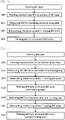
- FIG. 1 An example of a method for manufacturing an SOI wafer, that is not part of the invention as claimed, will be described with reference to the flow diagram of FIG. 1 .
- an SOI layer is formed on a wafer at first, and then the SOI film thickness before the thinning step is measured ( FIG. 1 (A1)).
- a rotational position of the SOI wafer in the thinning step is determined on the basis of a radial SOI film thickness distribution obtained in the measuring of the film thickness of the step (A1) and a previously determined radial stock removal distribution in the thinning step, and the SOI wafer is rotated around the central axis thereof so as to bring the SOI wafer to the determined rotational position ( FIG. 1 (A2)). Then, the SOI layer of the SOI wafer rotated in the step (A2) is thinned ( FIG. 1 (A3)).
- the method for forming an SOI layer is not particularly limited, but the SOI layer is preferably formed by an ion implantation delamination method including a step of bonding a bond wafer having a micro bubble layer formed by an ion implantation with a base wafer to be a support substrate, and a step of delaminating the bond wafer along the micro bubble layer as a boundary to form a thin film on the base wafer, for example.
- the ion implantation delamination method can give an SOI wafer having an extremely thin SOI layer with relatively small radial film thickness distribution.
- the SOI film thickness is measured on the SOI wafer having the SOI layer before the thinning step to adjust the SOI film thickness.
- the measurement of the SOI film thickness before the thinning step is not particularly limited, and can be performed by a known method.
- a rotational position of the SOI wafer in the thinning step is determined on the basis of a radial SOI film thickness distribution obtained in the measuring of the film thickness of the step (A1) and a previously determined radial stock removal distribution in the thinning step, and the SOI wafer is rotated around the central axis thereof so as to bring the SOI wafer to the determined rotational position.
- the radial stock removal distribution may be determined by film thinning so as to make the SOI film thickness be a target value using a thinning method used in a thinning step of the actual subsequent step (such as a batch processing type cleaning machine and a single wafer processing type cleaning machine), and by measuring the SOI film thickness after the film thinning, for example.
- a thinning method used in a thinning step of the actual subsequent step such as a batch processing type cleaning machine and a single wafer processing type cleaning machine
- the rotational position of the SOI wafer in the thinning step is determined on the basis of the radial SOI film thickness distribution obtained in the measuring of the film thickness of the step (A1) and the previously determined radial stock removal distribution in the thinning step.
- the radial film thickness uniformity of the SOI layer after the thinning step is degraded when a portion with a thin film thickness of the SOI layer before the thinning step becomes a portion where the stock removal in the thinning step is large, for example.
- the rotational position may be determined so as to make the wafer to have small radial variance of difference between the film thickness of the SOI layer before the thinning step and the stock removal in the thinning step. More specifically, as the criterion for determining the rotational position, one of the following three criteria is used.
- the rotational position is determined to a position where an area showing the maximum value of the radial SOI film thickness distribution obtained in the measuring of the film thickness corresponds to an area showing the maximum value of the previously determined radial stock removal distribution in the thinning step.
- the rotational position is determined to a position where an area showing the minimum value of the radial SOI film thickness distribution obtained in the measuring of the film thickness corresponds to an area showing the minimum value of the previously determined radial stock removal distribution in the thinning step.
- the rotational position is determined by calculating the respective radial SOI film thickness distributions after the thinning step when altering the rotational position by a prescribed angle on the basis of the radial SOI film thickness distribution obtained by the measuring of the film thickness and the previously determined radial stock removal distribution in the thinning step, followed by fixing the rotational position to a position where a difference between the calculated radial maximum value and the calculated radial minimum value of the SOI film thickness after the thinning step is minimum.
- step (A1)) it is preferable to perform the step of measuring the SOI film thickness before the thinning step (step (A1)) and the subsequent step of rotating the SOI wafer (step (A2)) in the same apparatus since the process can be simplified.
- the rotational position of a wafer is determined at a time of collecting the wafer immediately after measuring the SOI film thickness on the basis of the measured radial SOI film thickness distribution and the previously determined radial stock removal distribution in the thinning step, the wafer is rotated with the wafer rotary mechanism in the SOI film thickness measuring device so as to bring the SOI wafer to the determined rotational position, and then the wafer is collected into a cleaning carrier of a cleaning machine used in the thinning step.
- This can perform the measuring of the SOI film thickness and the rotation of the wafer before the thinning step in the same apparatus, and can simplify the process.
- the thinning is performed on the SOI layer of the SOI wafer rotated in the step (A2).
- the method for thinning an SOI layer to adjust the SOI film thickness it is effective to adopt thinning by cleaning (etching) with a batch processing type cleaning machine, but not limited thereto.
- thinning methods such as cleaning (etching) with a single wafer processing type cleaning machine, a sacrificial oxidation process (batch processing, single wafer processing), gas etching with a gas (e.g., HCl), dry etching, wet etching, and flattening accompanied with thinning of the SOI layer by heat treatment in a reductive atmosphere such as hydrogen or argon.
- a gas e.g., HCl
- dry etching dry etching
- wet etching wet etching
- flattening accompanied with thinning of the SOI layer by heat treatment in a reductive atmosphere such as hydrogen or argon.
- SC1 solution mixed aqueous solution of NH 4 OH and H 2 O 2 .
- the radial stock removal distribution of Si etching is liable to form deviation at the upper and lower portions in a water tank, and the etching stock removal at a portion immersed to an upper portion of the water tank tends to be smaller than the etching stock removal at a portion immersed to an lower portion in the water tank.
- the chemical solution is heated in the circulation line and supplied from the lower portion in the water tank, the immersion time differs within the wafer surfaces and gets longer at the lower portion of the wafer since the wafer is put and taken out of the liquid surface, etc.
- a rotational position is determined so as to bring the portion with a thin SOI film thickness to the upper side in a water tank of a batch processing type cleaning machine before the cleaning with the batch processing type cleaning machine, for example, on the basis of a radial SOI film thickness distribution obtained in the measuring of the SOI film thickness before the thinning step and the foregoing deviation of a radial stock removal distribution of etching; and the wafer is previously rotated before the batch processing type cleaning and introduced into a cleaning carrier.
- the rotational position of each SOI wafer in a batch can be determined on the basis of the measured SOI film thickness before the thinning step, and the wafer can be rotated to each determined rotational position, and then introduced into the cleaning carrier and cleaned. Accordingly, it is possible to improve the radial distribution of each wafer with highly accuracy and to further simplify the process.
- a rotational position is determined so as to bring the portion with a thin SOI film thickness to the upper side in a water tank of a single wafer processing type cleaning machine before the cleaning with the single wafer processing type cleaning machine on the basis of a radial SOI film thickness distribution obtained in the measuring of the SOI film thickness before the thinning step and the foregoing deviation of a radial stock removal distribution of etching; and the wafer is previously rotated before the single wafer processing type cleaning and introduced into a cleaning carrier.
- the wafer is rotated continuously during the thinning step. Accordingly, the radial stock removal distribution in the thinning step becomes a concentric circle shape, and the radial film thickness distribution is not largely influenced by rotating the wafer before the thinning step around the central axis thereof to the determined rotational position.
- the continuous rotation of the wafer is eccentric during the thinning step, the radial stock removal distribution differs from the concentric circle.
- FIGS. 2 each shows an example of a radial SOI film thickness distribution in each stage and a previously determined radial stock removal distribution in the thinning step when an SOI wafer is actually manufactured by the flow of FIG. 1.
- FIG. 2 (a) shows the radial SOI film thickness distribution before the thinning step.
- FIG. 2 (b) shows the previously determined radial stock removal distribution in the thinning step.
- FIG. 2 (c) shows the radial SOI film thickness distribution after rotating the wafer.
- FIG. 2 (d) shows the radial SOI film thickness distribution after the thinning step.
- an SOI layer is formed on a wafer.
- SOI film thicknesses before the thinning step are measured to obtain a radial SOI film thickness distribution like FIG. 2 (a) as the step (A1).
- the average value of the SOI film thickness is 16.7 nm
- the radial film thickness distribution is 0.59 nm, which reveals that the SOI film is thinnest at the measuring position of 7:30 o'clock (the clockwise position of 225° when the upper end of the wafer is set to 0°).
- the rotational position of the wafer in the thinning step is determined as the step (A2).
- the radial stock removal distribution in the thinning step like FIG. 2 (b) is determined by previously measuring the radial stock removal distribution when the SOI film is thinned to a thickness of 12.0 nm with SC1 solution using a batch processing type cleaning machine.
- the average stock removal is 4.7 nm
- the radial stock removal distribution (stock removal Range: radial maximum value - radial minimum value of the stock removal) is 0.18 nm, which reveals that the stock removal is smallest at the upper side in a cleaning carrier.
- the rotational position of the wafer in batch processing type cleaning is determined on the basis of the radial SOI film thickness distribution ( FIG. 2 (a) ) obtained in the step (A1) and the radial stock removal distribution ( FIG. 2 (b) ) in the thinning step obtained as described above.
- the rotational position can be determined to any value on the basis of the foregoing criteria, for example.
- the measuring position of 7:30 o'clock, at which the SOI film thickness is thinnest is set to the upper side in the cleaning carrier, at which the stock removal is smallest.
- the wafer is rotated clockwise by 135° so as to bring the measuring position of 7:30 o'clock, at which the SOI film thickness is thinnest, to the upper side (at a position of 0 o'clock) in the cleaning carrier ( FIG. 2 (c) ).
- This rotation of the wafer may be performed in the SOI film thickness measuring device used in the step (A1) as described above, or may be performed separately after the wafer is pulled out from the SOI film thickness measuring device.
- the wafer rotated clockwise by 135° as in FIG. 2 (c) is transferred to the cleaning carrier and thinned to have an SOI film thickness of 12.0 nm with SC1 solution using a batch processing type cleaning machine as the step (A3) .
- the average value of the SOI film thickness was 12.0 nm and the radial film thickness distribution (film thickness Range) was 0.56 nm as in FIG. 2 (d) , which revealed that it is possible to improve the radial film thickness distribution from that before the thinning step, and to produce an SOI wafer with excellent radial film thickness uniformity after the thinning step by performing the thinning step as a flow of FIG. 1 .
- the method for manufacturing an SOI wafer can produce an SOI wafer with an excellent radial film thickness uniformity of the SOI layer after the thinning step to adjust the SOI film thickness.
- the present invention provides a method for manufacturing an SOI wafer having an SOI layer including a thinning step to adjust an SOI film thickness of the SOI wafer, comprising the steps as defined in the claims.
- FIG. 3 (B1) An example of such a method for manufacturing an SOI wafer is described with reference to the flow diagram of FIG. 3 .
- an SOI layer is formed on a wafer at first, and then a thermal oxide film is formed on the surface of the SOI layer by heat treatment under an oxidizing gas atmosphere ( FIG. 3 (B0)). Subsequently, the SOI film thickness before the thinning step is measured with the thermal oxide film remaining ( FIG. 3 (B1)).
- a rotational position of the SOI wafer in the thinning step is determined on the basis of a radial SOI film thickness distribution obtained in the measuring of the film thickness of the step (B1) and a previously determined radial stock removal distribution in the thinning step, and the SOI wafer is rotated around the central axis thereof so as to bring the SOI wafer to the determined rotational position ( FIG. 3 (B2)) as further defined in the claims.
- the SOI layer is thinned by batch processing type cleaning which includes removing the thermal oxide film on the surface of the SOI layer and etching of the SOI layer of the SOI wafer rotated in the step (B2) while controlling the etching amount of the SOI layer on the basis of the SOI film thickness obtained in the step (B1) ( FIG. 3 (B3)) as further defined in the claims.
- the formation of a thermal oxide film is performed by a method of heat treatment under an oxidizing gas atmosphere, and can be performed by a known method.
- the formation of the SOI layer, the step (B1), and the step (B2) may be performed in a similar manner to the foregoing formation of the SOI layer, the step (A1), and the step (A2) respectively.
- the SOI layer is thinned while controlling the etching amount of the SOI layer on the basis of the SOI film thickness (e.g., the radial average value) obtained in the step (B1) by batch processing type cleaning which includes removing the thermal oxide film on the surface of the SOI layer and etching of the SOI layer of the SOI wafer rotated in the step (B2) as defined in the claims.
- the specific thinning method by batch processing type cleaning includes etching of the SOI layer by immersing the SOI wafer in a SC1 solution inside a water tank, such as by using a batch processing type cleaning machine.
- Such a method for manufacturing an SOI wafer can produce an SOI wafer with an excellent radial film thickness uniformity of the SOI layer after the thinning step by removing the thermal oxide film formed on the surface of the SOI layer before the thinning step, and then etching to adjust the film thickness.
- the present invention also provides a method for manufacturing an SOI wafer as defined in the claims, wherein the method comprises as the step B3,
- FIG. 4 An example of such a method for manufacturing an SOI wafer is described with reference to the flow diagram of FIG. 4 .
- an SOI layer is formed on a wafer at first, and then a thermal oxide film is formed on the surface of the SOI layer by heat treatment under an oxidizing gas atmosphere ( FIG. 4 (C0)). Subsequently, the SOI film thickness before the first thinning step is measured with the thermal oxide film remaining ( FIG. 4 (C1)).
- the rotational position of the SOI wafer in the first thinning step is determined on the basis of a radial SOI film thickness distribution obtained in the measuring of the film thickness of the step (C1) and a previously determined radial stock removal distribution in the first thinning step, and the SOI wafer is rotated around the central axis thereof so as to bring the SOI wafer to the determined rotational position ( FIG. 4 (C2)) as further defined in the claims.
- the SOI layer is thinned to be thicker than a final target value of the film thickness by batch processing type cleaning which includes removing the thermal oxide film on the surface of the SOI layer and etching of the SOI layer of the SOI wafer rotated in the step (C2) while controlling the etching amount of the SOI layer on the basis of the SOI film thickness obtained in the step (C1) (the first thinning step; FIG. 4 (C3)) as further defined in the claims. Then, the SOI film thickness of the SOI wafer after the first thinning step is measured ( FIG. 4 (C4)).
- the rotational position of the SOI wafer in the second thinning step is determined on the basis of a radial SOI film thickness distribution obtained in the measuring of the film thickness of the step (C4) and a previously determined radial stock removal distribution in the second thinning step, and the SOI wafer is rotated around the central axis thereof so as to bring the SOI wafer to the determined rotational position ( FIG. 4 (C5)) as further defined in the claims.
- the SOI layer is thinned to be the final target value of the film thickness by cleaning which includes etching of the SOI layer of the SOI wafer rotated in the step (C5) while controlling the etching amount of the SOI layer on the basis of the SOI film thickness obtained in the step (C4) (the second thinning step; FIG. 4 (C6)) as further defined in the claims.
- the formation of the SOI layer, the step (C1), and the step (C2) may be performed in a similar manner to the foregoing formation of the SOI layer, the step (A1), and the step (A2) respectively.
- the step (C0) may be performed in a similar manner to the foregoing step (B0).
- the SOI layer is thinned so as to be thicker than a final target value of the film thickness while controlling the etching amount of the SOI layer on the basis of the SOI film thickness (e.g., the radial average value) obtained in the step (C1) by batch processing type cleaning which includes removing the thermal oxide film on the surface of the SOI layer and etching of the SOI layer of the SOI wafer rotated in the step (C2).
- the step (C3) is performed in a similar manner to the foregoing step (B3), the SOI layer is thinned so as to be thicker than the final target value in the first thinning step and is thinned so as to be the final target value in the second thinning step described later.
- step (C4) the SOI film thickness on the SOI wafer after the first thinning step is measured.
- the step (C4) may be performed in a similar manner to the foregoing step (A1).
- a rotational position of the SOI wafer in the second thinning step is determined on the basis of a radial SOI film thickness distribution obtained in the measuring of the film thickness of the step (C4) and a previously determined radial stock removal distribution in the second thinning step, and the SOI wafer is rotated around the central axis thereof so as to bring the SOI wafer to the determined rotational position.
- the step (C5) is performed as defined in step (B2).
- the SOI layer is thinned so as to be the final target value of the film thickness while controlling the etching amount of the SOI layer on the basis of the SOI film thickness (e.g., the radial average value) obtained in the step (C4) by cleaning which includes etching of the SOI layer of the SOI wafer rotated in the step (C5).
- the cleaning of the step (C6) may be performed in a similar manner to the foregoing step (A3), and is preferably performed by single wafer processing type cleaning.
- Such a method for manufacturing an SOI wafer can produce an SOI wafer with an excellent radial film thickness uniformity of the SOI layer after the thinning step by a two-stage thinning process including the first thinning step to remove the thermal oxide film formed on the surface of the SOI layer before the thinning step, and the second thinning step to adjust the film thickness to the target value by etching.
- inventive method for manufacturing an SOI wafer described above can be applied to various methods for manufacturing an SOI wafer such as Smart Cut method, SIMOX (Separation by IMplanted Oxygen) method, and rTCCP (room-Temerature Controlled Cleave Process) method.
- Smart Cut method SIMOX (Separation by IMplanted Oxygen) method
- rTCCP room-Temerature Controlled Cleave Process
- the inventive method for manufacturing an SOI wafer can produce an SOI wafer with an excellent radial film thickness uniformity of the SOI layer after the thinning step while controlling the film thickness of the SOI layer with high accuracy, for example, in a method for thinning an SOI layer by removing a thermal oxide film formed on the surface of the SOI layer and a method for thinning an SOI layer by a two-stage thinning process including removal of a thermal oxide film and adjustment of the film thickness. Accordingly, such methods are suitable for forming an FD-SOI wafer, which is required to have extremely high radial film thickness uniformity of the SOI layer.
- the inventive methods can improve the radial SOI film thickness distribution, and can improve the yield of producing an SOI wafer having a target SOI film thickness. As a result, it is possible to reduce the cost of the process.
- the present invention will be specifically described with reference to Examples and Comparative Example, but the present invention is not limited thereto.
- the thinning was performed by the first and the second thinning step with the final target value of the SOI layer being set to 12.0 nm.
- the wafer was rotated clockwise by 135° and then transferred to a cleaning carrier with a transfer machine (out of the SOI film thickness measuring device) after measuring the SOI film thickness so as to bring the area with thinnest radial film thickness of the SOI layer to the upper side in a cleaning tank (i.e., the area where the stock removal is smallest) to perform the first thinning step.
- the wafers were subjected to batch processing type cleaning (cleaning for removing the oxide film) as the first thinning step so as to have an SOI film thickness of 13.0 nm (thicker than the final target value) in the cleaning conditions shown in Table 1 with a batch processing type cleaning machine in which plural wafers are integrated into a cassette as one batch.
- each wafer was rotated and then transferred to a cleaning carrier with a transfer machine (out of the SOI film thickness measuring device) after measuring the SOI film thickness so as to bring the area with thinnest radial film thickness of the SOI layer to the upper side in a cleaning tank (i.e., the area where the stock removal is smallest) to perform the second thinning step.
- the wafer was subjected to batch processing type cleaning (cleaning for adjusting the film thickness) in the cleaning conditions shown in Table 1 with SC1 solution using a batch processing type cleaning machine as the second thinning step.
- the cleaning carriers were divided to house the SOI wafers in which the radial average value of the SOI film thickness differ from each other by every 0.1 nm on the basis of the measured results of the SOI film thickness after the first thinning step, and the SOI wafer was thinned to the target value (12.0 nm) with the immersion time to SC1 in the cleaning for adjusting the film thickness being altered in each carrier.
- the SC1 was the same one used in the first thinning step.
- Each SOI layer was thinned by the same procedure with Example 1 except for performing the rotation of the SOI wafer before the first thinning step and the rotation of the SOI wafer before the second thinning step by using a wafer rotary mechanism in the SOI film thickness measuring device without providing the step of rotating the wafer separately.
- each wafer was rotated so as to bring the area with thinnest radial film thickness of the SOI layer to the upper side in a cleaning tank (i.e., the area where the stock removal is smallest) to perform the thinning step as in Example 1.
- Each SOI layer was thinned by the same procedure with Example 1 except for performing the rotation of the SOI wafer before the first thinning step and the rotation of the SOI wafer before the second thinning step by using a wafer rotary mechanism in the SOI film thickness measuring device without providing the step of rotating the wafer separately, and performing the second thinning step by single wafer processing cleaning of a wafer immersion type.
- each wafer was rotated so as to bring the area with thinnest radial film thickness of the SOI layer to the upper side in a cleaning tank (i.e., the area where the stock removal is smallest) to perform the thinning step as in Example 1.
- the SOI wafer was thinned to the target value (12.0 nm) with the immersion time to SC1 being altered for each wafer in accordance with the SOI film thickness on the basis of the measured results of the SOI film thickness after the first thinning step.
- the SC1 was the same one used in the first thinning step.
- Each SOI layer was thinned by the same procedure with Example 1 except that the rotation of the SOI wafer before the first thinning step and the rotation of the SOI wafer before the second thinning step were not performed.
- the experimental conditions, the measured results of the SOI film thickness in each stage, and the calculated yields are shown in Table 1.
- the film thickness Range and the yields did not show differences between the case of rotating the wafer in the SOI film thickness measuring device at the time of collecting the wafer for measuring the SOI film thickness (Example 2) and the case of rotating the wafer separately after measuring the SOI film thickness (Example 1).
- the inventive method for manufacturing an SOI wafer can produce an SOI wafer with an excellent radial film thickness uniformity of the SOI layer after the thinning step to adjust the SOI film thickness.
Landscapes
- Engineering & Computer Science (AREA)
- Power Engineering (AREA)
- Manufacturing & Machinery (AREA)
- Computer Hardware Design (AREA)
- Microelectronics & Electronic Packaging (AREA)
- General Physics & Mathematics (AREA)
- Physics & Mathematics (AREA)
- Condensed Matter Physics & Semiconductors (AREA)
- Chemical & Material Sciences (AREA)
- Chemical Kinetics & Catalysis (AREA)
- General Chemical & Material Sciences (AREA)
- Inorganic Chemistry (AREA)
- Testing Or Measuring Of Semiconductors Or The Like (AREA)
- Mechanical Treatment Of Semiconductor (AREA)
- Weting (AREA)
Description
- The present invention relates to a method for manufacturing an SOI wafer, especially to a method for manufacturing an SOI wafer required to have extremely high uniformity of the SOI film thickness called FD-SOI (Fully Depleted Silicon-On-Insulator).
- Previously, as one of the thinning method of SOI layer of an SOI wafer having the SOI layer, it has been performed a process of subjecting an SOI wafer to heat treatment in a batch processing type heat treatment furnace, thereby oxidizing and modifying Si on the SOI layer surface to an oxide film, and then removing this oxide film (so-called sacrificial oxidation process).
- For thinning the SOI film thickness precisely to an target value by this method, the thickness of the oxide film have to be accurately controlled so as to be a target value. Actually, however, the oxidation rate changes due to fluctuation of the atmospheric pressure during the oxidation, and it is very difficult to accurately control the oxide film thickness grown by the heat treatment thereby. Accordingly, in film thinning through forming and removing an oxide film, the process has been performed by thinning through forming and removing the oxide film so as to have an SOI film thickness slightly (about 3 nm) thicker than the target value after the thinning step, and thinning by subsequent etching separately performed with the etching time being controlled so as to have the target value.
- This two stage thinning process has been performed such that the oxide film after the oxidation is removed, and then the SOI film thickness is measured to set the stock removal in the next stage of the etching stage on the basis of the value, as described in Patent Document 1.
- In the two stage thinning process through forming and removing the oxide film together with etching, it has been proposed a method in which the thickness of an SOI layer is measured after the oxidation with the thermal oxide film remaining, and on the basis of the measured film thickness of the SOI layer, the removal of the oxide film, etching, and further cleaning stage are performed in one batch treatment of cleaning to shorten the process.
- It has also been proposed a method of controlling the thinning of an SOI layer by using a single wafer processing type etching apparatus in addition to forming and removing of an oxide film and thinning with a batch processing type cleaning machine (Patent Document 2).
- When the film thickness of an SOI layer is controlled with high accuracy by these methods, however, radial stock removal variance arises in the thinning step such as forming and removing an oxide film, etching, etc. to degrade the radial film thickness distribution of the SOI layer after the thinning step. It is not possible to meet the needs for the uniformity of the film thickness when highly accurate uniformity of the film thickness is required, for example when all of the points on a wafer surface are required to have a thickness within ±0.5 nm of the target SOI film thickness such as in an FD-SOI wafer.
US 2010/0129941 A1 discloses a processing method that includes an oxidation step of forming a natural oxide film on a surface of the SOI layer and an etching step of removing, with etching liquid, the natural oxide film formed in a local thick film portion of the SOI layer while leaving a part (e.g., 1 Å to 2 Å) of the thickness.EP 1 480 265 A2 discloses a substrate manufacturing method comprising: a preparation step of preparing a substrate which has a silicon layer on an insulating layer; and a thinning step of thinning the silicon layer on the insulting layer to a desired thickness, wherein in the thinning step, a unit thinning step including an oxidation step of oxidizing a surface of the silicon layer by a predetermined thickness, and a removal step of selectively removing silicon oxide formed in the oxidation step is performed not less than twice.US 2005/0015736 A1 discloses an in-plane distribution data compression method used in a production process of a semiconductor device, comprising the steps of: performing a process over a substrate; measuring an in-plane distribution over the substrate; calculating a model formula of the in-plane distribution from measurement data obtained by the measurement; comparing the measurement data with the model formula to calculate a set of parameters of the model formula; and storing the parameters as data of the in-plane distribution over the substrate, wherein the measurement data includes measurement coordinates over the substrate, and the model formula is obtained by modeling the tendency that the in-plane distribution concentrically varies and the tendency that the in-plane distribution varies along a diameter direction.JP 2001-284305 A -
- Patent Document 1:
JP 2007-266059 A - Patent Document 2:
JP 2010-092909 A - Patent Document 3:
US 2010/0129941 A1 - Patent Document 4:
EP 1 480 265 A2 - Patent Document 5:
US 2005/0015736 A1 - Patent Document 6:
JP 2001-284-305 A - The present invention was accomplished in view of the above-described problems. It is an object of the present invention to provide a method for manufacturing an SOI wafer which can produce an SOI wafer with an excellent radial film thickness uniformity of the SOI layer after the thinning step.
- The present invention provides a method for manufacturing a silicon on insulator, SOI, wafer having an SOI layer including a thinning step to adjust an SOI film thickness of the SOI wafer, comprising the steps of:
- step B0 - heat treatment under an oxidizing gas atmosphere to form a thermal oxide film on a surface of the SOI layer;
- step B1 - measuring the SOI film thickness of the SOI wafer having the thermal oxide film formed in the step B0 with the thermal oxide film remaining;
- step B2 - determining a rotational position of the SOI wafer in the thinning step on the basis of a radial SOI film thickness distribution obtained in the measuring of the film thickness of the step B1 and a previously determined radial stock removal distribution in the thinning step, and rotating the SOI wafer around the central axis thereof so as to bring the SOI wafer to the determined rotational position; and
- step B3 - thinning the SOI layer by batch processing cleaning which includes removing the thermal oxide film on the surface of the SOI layer and etching of the SOI layer of the SOI wafer rotated in the step B2, with the etching amount of the SOI layer being controlled on the basis of the SOI film thickness obtained in the step B1, wherein the etching in the batch processing cleaning is performed by immersing the SOI wafer in a SC1 solution inside a water tank, and
- wherein the rotational position is determined to a position where an area showing the maximum value of the radial SOI film thickness distribution obtained in the measuring of the film thickness corresponds to an area showing the maximum value of the previously determined radial stock removal distribution in the thinning step, or
- wherein the rotational position is determined to a position where an area showing the minimum value of the radial SOI film thickness distribution obtained in the measuring of the film thickness corresponds to an area showing the minimum value of the previously determined radial stock removal distribution in the thinning step, or
- wherein the rotational position is determined to a position where a difference between a calculated radial maximum value and a calculated radial minimum value of the SOI film thickness after the thinning step is minimum in calculation of the respective radial SOI film thickness distributions after the thinning step when altering the rotational position by a prescribed angle on the basis of the radial SOI film thickness distribution obtained by the measuring of the film thickness and the previously determined radial stock removal distribution in the thinning step.
- Such a method for manufacturing an SOI wafer can produce an SOI wafer with an excellent radial film thickness uniformity of the SOI layer after the thinning step by removing the thermal oxide film formed on the surface of the SOI layer before the thinning step to adjust the SOI film thickness, and by etching to adjust the film thickness.
- The present invention also provides a method for manufacturing an SOI wafer as defined in the claims, wherein the method for manufacturing an SOI wafer comprises as step B3, step C3 - thinning the SOI layer to be thicker than a final target value of the film thickness as the first thinning step by batch processing cleaning which includes removing the thermal oxide film on the surface of the SOI layer and etching of the SOI layer of the SOI wafer rotated in the step B2, with the etching amount of the SOI layer being controlled on the basis of the SOI film thickness obtained in the step B1; and
further comprises: - step C4 - measuring the SOI film thickness of the SOI wafer after the first thinning step;
- step C5 - determining a rotational position of the SOI wafer in the second thinning step on the basis of a radial SOI film thickness distribution obtained in the measuring of the film thickness of the step C4 and a previously determined radial stock removal distribution in the second thinning step, and rotating the SOI wafer around the central axis thereof so as to bring the SOI wafer to the determined rotational position, wherein the rotational position is determined as defined in step B2; and
- step C6 - thinning the SOI layer to be the final target value of the film thickness as the second thinning step by cleaning which includes etching of the SOI layer of the SOI wafer rotated in the step C5, with the etching amount of the SOI layer being controlled on the basis of the SOI film thickness obtained in the step C4.
- Such a method for manufacturing an SOI wafer can produce an SOI wafer with an excellent radial film thickness uniformity of the SOI layer after the thinning step by a two-stage thinning process including the first thinning step to remove the thermal oxide film formed on the surface of the SOI layer before the thinning step to adjust the SOI film thickness, and the second thinning step to adjust the film thickness to the target value by etching.
- In this case, the cleaning of the step C6 is preferably performed by single wafer processing.
- The second thinning step performed by single wafer processing makes it possible to produce an SOI wafer while further improving the controllability of the film thickness of the SOI layer after the thinning step.
- The rotational position is determined to a position where an area showing the maximum value of the radial SOI film thickness distribution obtained in the measuring of the film thickness corresponds to an area showing the maximum value of the previously determined radial stock removal distribution in the thinning step, or the rotational position is determined to a position where an area showing the minimum value of the radial SOI film thickness distribution obtained in the measuring of the film thickness corresponds to an area showing the minimum value of the previously determined radial stock removal distribution in the thinning step, or the rotational position is determined to a position where a difference between a calculated radial maximum value and a calculated radial minimum value of the SOI film thickness after the thinning step is minimum in calculation of the respective radial SOI film thickness distributions after the thinning step when altering the rotational position by a prescribed angle on the basis of the radial SOI film thickness distribution obtained by the measuring of the film thickness and the previously determined radial stock removal distribution in the thinning step.
- By the thinning step with rotating the SOI wafer so as to bring the SOI wafer to the rotational position determined by such criteria, it is possible to produce an SOI wafer with an excellent radial film thickness uniformity of the SOI layer after the thinning step more securely.
- It is preferable to perform the step of measuring the SOI film thickness before the thinning step and the subsequent step of rotating the SOI wafer in the same apparatus.
- The process can be simplified by performing these steps in one apparatus as described above.
- It is also preferable to form the SOI layer by an ion implantation delamination method including at least the steps of:
- bonding a bond wafer having a micro bubble layer formed by an ion implantation with a base wafer to be a support substrate, and
- delaminating the bond wafer along the micro bubble layer as a boundary to form a thin film on the base wafer.
- As described above, the ion implantation delamination method can be suitably used for forming the SOI layer in the inventive method for manufacturing an SOI wafer.
- The etching in the batch processing cleaning of step B3 is performed by immersing the SOI wafer in a SC1 solution inside a water tank.
- As described above, SC1 solution can be suitably used for the thinning step in the inventive method for manufacturing an SOI wafer.
- As described above, the inventive method for manufacturing an SOI wafer can produce an SOI wafer with an excellent radial film thickness uniformity of the SOI layer after the thinning step while controlling the film thickness of the SOI layer with high accuracy, for example, in a method for thinning an SOI layer by removing a thermal oxide film formed on the surface of the SOI layer and a method for thinning an SOI layer by a two-stage thinning process including removal of a thermal oxide film and adjustment of the film thickness. Accordingly, such methods are suitable for forming an FD-SOI wafer, which is required to have extremely high radial film thickness uniformity of the SOI layer. The inventive methods can improve the radial SOI film thickness distribution, and can improve the yield of producing an SOI wafer having a target SOI film thickness. As a result, it is possible to reduce the cost of the process.
-
-
FIG. 1 is a flow diagram showing an example of a method for manufacturing an SOI wafer that is not part of the invention as claimed; -
FIGS. 2 are diagrams each showing an example of a radial SOI film thickness distribution in each stage and a previously determined radial stock removal distribution in the thinning step when an SOI wafer is manufactured by the flow ofFIG. 1 , in which (a) shows the radial SOI film thickness distribution before the thinning step, (b) shows the previously determined radial stock removal distribution in the thinning step, (c) shows the radial SOI film thickness distribution after rotating the wafer, and (d) shows the radial SOI film thickness distribution after the thinning step; -
FIG. 3 is a flow diagram showing an example of the inventive method for manufacturing an SOI wafer; -
FIG. 4 is a flow diagram showing another example of the inventive method for manufacturing an SOI wafer. - As described above, it has been desired to develop a method for manufacturing an SOI wafer which can produce an SOI wafer with an excellent radial film thickness uniformity of the SOI layer after the thinning step to adjust the SOI film thickness.
- The present inventors has diligently studied to accomplish the above-mentioned objects and consequently found that an SOI layer before the thinning step contains deviation in the radial distribution, and a radial stock removal distribution in the thinning step also contains deviation, thereby the radial film thickness uniformity of the SOI layer after the thinning step can degrade when a portion with a thin film thickness of the SOI layer before the thinning step becomes a portion where the stock removal in the thinning step is large, for example. On the basis of this respect, the present inventors also found that the radial film thickness uniformity of the SOI layer after the thinning step can be improved by measuring the SOI film thickness before the thinning step, determining a rotational position of the SOI wafer in the thinning step on the basis of the measured radial SOI film thickness distribution and a previously determined radial stock removal distribution in the thinning step, and performing the thinning step in a state in which the SOI wafer is rotated around the central axis thereof so as to be set to such a rotational position; thereby brought the present invention to completion.
- That is, the present invention is a method for manufacturing an SOI wafer as defined in the claims.
- Hereinafter, methods for manufacturing an SOI wafer and the present invention will be described specifically, but the present invention is defined in the claims.
- An example of a method for manufacturing an SOI wafer, that is not part of the invention as claimed, will be described with reference to the flow diagram of
FIG. 1 . In the method for manufacturing an SOI wafer ofFIG. 1 , an SOI layer is formed on a wafer at first, and then the SOI film thickness before the thinning step is measured (FIG. 1 (A1)). Subsequently, a rotational position of the SOI wafer in the thinning step is determined on the basis of a radial SOI film thickness distribution obtained in the measuring of the film thickness of the step (A1) and a previously determined radial stock removal distribution in the thinning step, and the SOI wafer is rotated around the central axis thereof so as to bring the SOI wafer to the determined rotational position (FIG. 1 (A2)). Then, the SOI layer of the SOI wafer rotated in the step (A2) is thinned (FIG. 1 (A3)). - Hereinafter, each step will be described more specifically.
- The method for forming an SOI layer is not particularly limited, but the SOI layer is preferably formed by an ion implantation delamination method including a step of bonding a bond wafer having a micro bubble layer formed by an ion implantation with a base wafer to be a support substrate, and a step of delaminating the bond wafer along the micro bubble layer as a boundary to form a thin film on the base wafer, for example. The ion implantation delamination method can give an SOI wafer having an extremely thin SOI layer with relatively small radial film thickness distribution.
- In the step (A1), the SOI film thickness is measured on the SOI wafer having the SOI layer before the thinning step to adjust the SOI film thickness. The measurement of the SOI film thickness before the thinning step is not particularly limited, and can be performed by a known method.
- In the step (A2), a rotational position of the SOI wafer in the thinning step is determined on the basis of a radial SOI film thickness distribution obtained in the measuring of the film thickness of the step (A1) and a previously determined radial stock removal distribution in the thinning step, and the SOI wafer is rotated around the central axis thereof so as to bring the SOI wafer to the determined rotational position.
- When previously determining the radial stock removal distribution in the thinning step to adjust the SOI film thickness, the radial stock removal distribution may be determined by film thinning so as to make the SOI film thickness be a target value using a thinning method used in a thinning step of the actual subsequent step (such as a batch processing type cleaning machine and a single wafer processing type cleaning machine), and by measuring the SOI film thickness after the film thinning, for example.
- The rotational position of the SOI wafer in the thinning step is determined on the basis of the radial SOI film thickness distribution obtained in the measuring of the film thickness of the step (A1) and the previously determined radial stock removal distribution in the thinning step. As described above, the radial film thickness uniformity of the SOI layer after the thinning step is degraded when a portion with a thin film thickness of the SOI layer before the thinning step becomes a portion where the stock removal in the thinning step is large, for example. Accordingly, the rotational position may be determined so as to make the wafer to have small radial variance of difference between the film thickness of the SOI layer before the thinning step and the stock removal in the thinning step. More specifically, as the criterion for determining the rotational position, one of the following three criteria is used.
- The rotational position is determined to a position where an area showing the maximum value of the radial SOI film thickness distribution obtained in the measuring of the film thickness corresponds to an area showing the maximum value of the previously determined radial stock removal distribution in the thinning step.
- The rotational position is determined to a position where an area showing the minimum value of the radial SOI film thickness distribution obtained in the measuring of the film thickness corresponds to an area showing the minimum value of the previously determined radial stock removal distribution in the thinning step.
- The rotational position is determined by calculating the respective radial SOI film thickness distributions after the thinning step when altering the rotational position by a prescribed angle on the basis of the radial SOI film thickness distribution obtained by the measuring of the film thickness and the previously determined radial stock removal distribution in the thinning step, followed by fixing the rotational position to a position where a difference between the calculated radial maximum value and the calculated radial minimum value of the SOI film thickness after the thinning step is minimum.
- It is possible to improve the radial SOI film thickness distribution or to minimize the degradation of the radial distribution due to the thinning step by performing the thinning step with the SOI wafer being rotated so as to be set to a rotation angle determined by any of the foregoing criteria.
- In this case, it is preferable to perform the step of measuring the SOI film thickness before the thinning step (step (A1)) and the subsequent step of rotating the SOI wafer (step (A2)) in the same apparatus since the process can be simplified. More specifically, when using an SOI film thickness measuring device equipped with a wafer rotary mechanism for an alignment in the step (A1), the rotational position of a wafer is determined at a time of collecting the wafer immediately after measuring the SOI film thickness on the basis of the measured radial SOI film thickness distribution and the previously determined radial stock removal distribution in the thinning step, the wafer is rotated with the wafer rotary mechanism in the SOI film thickness measuring device so as to bring the SOI wafer to the determined rotational position, and then the wafer is collected into a cleaning carrier of a cleaning machine used in the thinning step. This can perform the measuring of the SOI film thickness and the rotation of the wafer before the thinning step in the same apparatus, and can simplify the process.
- In the step (A3), the thinning is performed on the SOI layer of the SOI wafer rotated in the step (A2). As the method for thinning an SOI layer to adjust the SOI film thickness, it is effective to adopt thinning by cleaning (etching) with a batch processing type cleaning machine, but not limited thereto. According to a desired stock removal, it is possible to adopt various thinning methods such as cleaning (etching) with a single wafer processing type cleaning machine, a sacrificial oxidation process (batch processing, single wafer processing), gas etching with a gas (e.g., HCl), dry etching, wet etching, and flattening accompanied with thinning of the SOI layer by heat treatment in a reductive atmosphere such as hydrogen or argon.
- It is preferable to perform the thinning step by immersing the SOI wafer in SC1 solution (mixed aqueous solution of NH4OH and H2O2).
- In cleaning (etching) with a batch processing type cleaning machine and SC1 solution, the radial stock removal distribution of Si etching is liable to form deviation at the upper and lower portions in a water tank, and the etching stock removal at a portion immersed to an upper portion of the water tank tends to be smaller than the etching stock removal at a portion immersed to an lower portion in the water tank. This is because the chemical solution is heated in the circulation line and supplied from the lower portion in the water tank, the immersion time differs within the wafer surfaces and gets longer at the lower portion of the wafer since the wafer is put and taken out of the liquid surface, etc.
- Accordingly, when the thinning step is performed by cleaning (etching) with a batch processing type cleaning machine and SC1 solution, it is possible to improve the radial SOI film thickness distribution after the thinning step with a batch processing type cleaning machine from that before the thinning step or to minimize degradation of the radial distribution after the thinning step by cleaning procedure described below: a rotational position is determined so as to bring the portion with a thin SOI film thickness to the upper side in a water tank of a batch processing type cleaning machine before the cleaning with the batch processing type cleaning machine, for example, on the basis of a radial SOI film thickness distribution obtained in the measuring of the SOI film thickness before the thinning step and the foregoing deviation of a radial stock removal distribution of etching; and the wafer is previously rotated before the batch processing type cleaning and introduced into a cleaning carrier.
- If the radial stock removal distribution in a batch processing type cleaning machine is previously examined and put onto a database, the rotational position of each SOI wafer in a batch can be determined on the basis of the measured SOI film thickness before the thinning step, and the wafer can be rotated to each determined rotational position, and then introduced into the cleaning carrier and cleaned. Accordingly, it is possible to improve the radial distribution of each wafer with highly accuracy and to further simplify the process.
- In a single wafer processing cleaning machine of a wafer immersion type, the radial stock removal distribution of Si etching is liable to form deviation at the upper and lower portions in a water tank as in the batch processing. Accordingly, it is possible to improve the radial SOI film thickness distribution after the thinning step with a single wafer processing type cleaning machine from that before the thinning step or to minimize degradation of the radial distribution after the thinning step by cleaning procedure described below: a rotational position is determined so as to bring the portion with a thin SOI film thickness to the upper side in a water tank of a single wafer processing type cleaning machine before the cleaning with the single wafer processing type cleaning machine on the basis of a radial SOI film thickness distribution obtained in the measuring of the SOI film thickness before the thinning step and the foregoing deviation of a radial stock removal distribution of etching; and the wafer is previously rotated before the single wafer processing type cleaning and introduced into a cleaning carrier.
- On the other hand, in a single wafer processing cleaning machine of a chemical solution-poring type in which a wafer is held horizontally and chemical solution is poured from an upper pipe, the wafer is rotated continuously during the thinning step. Accordingly, the radial stock removal distribution in the thinning step becomes a concentric circle shape, and the radial film thickness distribution is not largely influenced by rotating the wafer before the thinning step around the central axis thereof to the determined rotational position. When the continuous rotation of the wafer is eccentric during the thinning step, the radial stock removal distribution differs from the concentric circle. Therefore, it is possible to improve the radial SOI film thickness distribution after the thinning step from that before the thinning step or to minimize degradation of the radial distribution after the thinning step by rotating a wafer before the thinning step to a desired rotational position.
- Hereinafter, the method for manufacturing an SOI wafer, that is not part of the invention as claimed, will be described more specifically with reference to
FIGS. 2. FIGS. 2 each shows an example of a radial SOI film thickness distribution in each stage and a previously determined radial stock removal distribution in the thinning step when an SOI wafer is actually manufactured by the flow ofFIG. 1. FIG. 2 (a) shows the radial SOI film thickness distribution before the thinning step.FIG. 2 (b) shows the previously determined radial stock removal distribution in the thinning step.FIG. 2 (c) shows the radial SOI film thickness distribution after rotating the wafer.FIG. 2 (d) shows the radial SOI film thickness distribution after the thinning step. - First, an SOI layer is formed on a wafer. Then, SOI film thicknesses before the thinning step are measured to obtain a radial SOI film thickness distribution like
FIG. 2 (a) as the step (A1). InFIG. 2 (a) , for example, the average value of the SOI film thickness is 16.7 nm, and the radial film thickness distribution (film thickness Range: radial maximum value - radial minimum value of the film thickness) is 0.59 nm, which reveals that the SOI film is thinnest at the measuring position of 7:30 o'clock (the clockwise position of 225° when the upper end of the wafer is set to 0°). - Then, the rotational position of the wafer in the thinning step is determined as the step (A2). Prior to that, the radial stock removal distribution in the thinning step like
FIG. 2 (b) is determined by previously measuring the radial stock removal distribution when the SOI film is thinned to a thickness of 12.0 nm with SC1 solution using a batch processing type cleaning machine. InFIG. 2 (b) , for example, the average stock removal is 4.7 nm, and the radial stock removal distribution (stock removal Range: radial maximum value - radial minimum value of the stock removal) is 0.18 nm, which reveals that the stock removal is smallest at the upper side in a cleaning carrier. - Subsequently, the rotational position of the wafer in batch processing type cleaning is determined on the basis of the radial SOI film thickness distribution (
FIG. 2 (a) ) obtained in the step (A1) and the radial stock removal distribution (FIG. 2 (b) ) in the thinning step obtained as described above. The rotational position can be determined to any value on the basis of the foregoing criteria, for example. In the batch processing type cleaning exemplified herein, the measuring position of 7:30 o'clock, at which the SOI film thickness is thinnest, is set to the upper side in the cleaning carrier, at which the stock removal is smallest. In this case, the wafer is rotated clockwise by 135° so as to bring the measuring position of 7:30 o'clock, at which the SOI film thickness is thinnest, to the upper side (at a position of 0 o'clock) in the cleaning carrier (FIG. 2 (c) ). This rotation of the wafer may be performed in the SOI film thickness measuring device used in the step (A1) as described above, or may be performed separately after the wafer is pulled out from the SOI film thickness measuring device. - Then, the wafer rotated clockwise by 135° as in
FIG. 2 (c) is transferred to the cleaning carrier and thinned to have an SOI film thickness of 12.0 nm with SC1 solution using a batch processing type cleaning machine as the step (A3) . - When the SOI film thickness distribution after the thinning step was measured, the average value of the SOI film thickness was 12.0 nm and the radial film thickness distribution (film thickness Range) was 0.56 nm as in
FIG. 2 (d) , which revealed that it is possible to improve the radial film thickness distribution from that before the thinning step, and to produce an SOI wafer with excellent radial film thickness uniformity after the thinning step by performing the thinning step as a flow ofFIG. 1 . - As described above, the method for manufacturing an SOI wafer can produce an SOI wafer with an excellent radial film thickness uniformity of the SOI layer after the thinning step to adjust the SOI film thickness.
- The present invention provides a method for manufacturing an SOI wafer having an SOI layer including a thinning step to adjust an SOI film thickness of the SOI wafer, comprising the steps as defined in the claims.
- An example of such a method for manufacturing an SOI wafer is described with reference to the flow diagram of
FIG. 3 . In the method for manufacturing an SOI wafer ofFIG. 3 , an SOI layer is formed on a wafer at first, and then a thermal oxide film is formed on the surface of the SOI layer by heat treatment under an oxidizing gas atmosphere (FIG. 3 (B0)). Subsequently, the SOI film thickness before the thinning step is measured with the thermal oxide film remaining (FIG. 3 (B1)). Then, a rotational position of the SOI wafer in the thinning step is determined on the basis of a radial SOI film thickness distribution obtained in the measuring of the film thickness of the step (B1) and a previously determined radial stock removal distribution in the thinning step, and the SOI wafer is rotated around the central axis thereof so as to bring the SOI wafer to the determined rotational position (FIG. 3 (B2)) as further defined in the claims. Subsequently, the SOI layer is thinned by batch processing type cleaning which includes removing the thermal oxide film on the surface of the SOI layer and etching of the SOI layer of the SOI wafer rotated in the step (B2) while controlling the etching amount of the SOI layer on the basis of the SOI film thickness obtained in the step (B1) (FIG. 3 (B3)) as further defined in the claims. - In the present invention, the formation of a thermal oxide film is performed by a method of heat treatment under an oxidizing gas atmosphere, and can be performed by a known method.
- Incidentally, the formation of the SOI layer, the step (B1), and the step (B2) may be performed in a similar manner to the foregoing formation of the SOI layer, the step (A1), and the step (A2) respectively.
- In the step (B3), the SOI layer is thinned while controlling the etching amount of the SOI layer on the basis of the SOI film thickness (e.g., the radial average value) obtained in the step (B1) by batch processing type cleaning which includes removing the thermal oxide film on the surface of the SOI layer and etching of the SOI layer of the SOI wafer rotated in the step (B2) as defined in the claims. The specific thinning method by batch processing type cleaning includes etching of the SOI layer by immersing the SOI wafer in a SC1 solution inside a water tank, such as by using a batch processing type cleaning machine.
- Such a method for manufacturing an SOI wafer can produce an SOI wafer with an excellent radial film thickness uniformity of the SOI layer after the thinning step by removing the thermal oxide film formed on the surface of the SOI layer before the thinning step, and then etching to adjust the film thickness.
- The present invention also provides a method for manufacturing an SOI wafer as defined in the claims, wherein the method comprises as the step B3,
- step C3 - thinning the SOI layer to be thicker than a final target value of the film thickness as the first thinning step by batch processing cleaning which includes removing the thermal oxide film on the surface of the SOI layer and etching of the SOI layer of the SOI wafer rotated in the step B2, with the etching amount of the SOI layer being controlled on the basis of the SOI film thickness obtained in the step B1;
- Step C4 - measuring the SOI film thickness of the SOI wafer after the first thinning step;
- Step C5 - determining a rotational position of the SOI wafer in the second thinning step on the basis of a radial SOI film thickness distribution obtained in the measuring of the film thickness of the step C4 and a previously determined radial stock removal distribution in the second thinning step, and rotating the SOI wafer around the central axis thereof so as to bring the SOI wafer to the determined rotational position, wherein the rotational position is determined as defined in step B2; and
- Step C6 - thinning the SOI layer to be the final target value of the film thickness as the second thinning step by cleaning which includes etching of the SOI layer of the SOI wafer rotated in the step C5, with the etching amount of the SOI layer being controlled on the basis of the SOI film thickness obtained in the step C4.
- An example of such a method for manufacturing an SOI wafer is described with reference to the flow diagram of
FIG. 4 . In the method for manufacturing an SOI wafer ofFIG. 4 , an SOI layer is formed on a wafer at first, and then a thermal oxide film is formed on the surface of the SOI layer by heat treatment under an oxidizing gas atmosphere (FIG. 4 (C0)). Subsequently, the SOI film thickness before the first thinning step is measured with the thermal oxide film remaining (FIG. 4 (C1)). Then, the rotational position of the SOI wafer in the first thinning step is determined on the basis of a radial SOI film thickness distribution obtained in the measuring of the film thickness of the step (C1) and a previously determined radial stock removal distribution in the first thinning step, and the SOI wafer is rotated around the central axis thereof so as to bring the SOI wafer to the determined rotational position (FIG. 4 (C2)) as further defined in the claims. Subsequently, the SOI layer is thinned to be thicker than a final target value of the film thickness by batch processing type cleaning which includes removing the thermal oxide film on the surface of the SOI layer and etching of the SOI layer of the SOI wafer rotated in the step (C2) while controlling the etching amount of the SOI layer on the basis of the SOI film thickness obtained in the step (C1) (the first thinning step;FIG. 4 (C3)) as further defined in the claims. Then, the SOI film thickness of the SOI wafer after the first thinning step is measured (FIG. 4 (C4)). Subsequently, the rotational position of the SOI wafer in the second thinning step is determined on the basis of a radial SOI film thickness distribution obtained in the measuring of the film thickness of the step (C4) and a previously determined radial stock removal distribution in the second thinning step, and the SOI wafer is rotated around the central axis thereof so as to bring the SOI wafer to the determined rotational position (FIG. 4 (C5)) as further defined in the claims. Then, the SOI layer is thinned to be the final target value of the film thickness by cleaning which includes etching of the SOI layer of the SOI wafer rotated in the step (C5) while controlling the etching amount of the SOI layer on the basis of the SOI film thickness obtained in the step (C4) (the second thinning step;FIG. 4 (C6)) as further defined in the claims. - Incidentally, the formation of the SOI layer, the step (C1), and the step (C2) may be performed in a similar manner to the foregoing formation of the SOI layer, the step (A1), and the step (A2) respectively. The step (C0) may be performed in a similar manner to the foregoing step (B0).
- In the step (C3), the SOI layer is thinned so as to be thicker than a final target value of the film thickness while controlling the etching amount of the SOI layer on the basis of the SOI film thickness (e.g., the radial average value) obtained in the step (C1) by batch processing type cleaning which includes removing the thermal oxide film on the surface of the SOI layer and etching of the SOI layer of the SOI wafer rotated in the step (C2). While the step (C3) is performed in a similar manner to the foregoing step (B3), the SOI layer is thinned so as to be thicker than the final target value in the first thinning step and is thinned so as to be the final target value in the second thinning step described later.
- In the step (C4), the SOI film thickness on the SOI wafer after the first thinning step is measured. The step (C4) may be performed in a similar manner to the foregoing step (A1).
- In the step (C5), a rotational position of the SOI wafer in the second thinning step is determined on the basis of a radial SOI film thickness distribution obtained in the measuring of the film thickness of the step (C4) and a previously determined radial stock removal distribution in the second thinning step, and the SOI wafer is rotated around the central axis thereof so as to bring the SOI wafer to the determined rotational position. The step (C5) is performed as defined in step (B2).
- In the step (C6), the SOI layer is thinned so as to be the final target value of the film thickness while controlling the etching amount of the SOI layer on the basis of the SOI film thickness (e.g., the radial average value) obtained in the step (C4) by cleaning which includes etching of the SOI layer of the SOI wafer rotated in the step (C5). It is to be noted that the cleaning of the step (C6) may be performed in a similar manner to the foregoing step (A3), and is preferably performed by single wafer processing type cleaning.
- Such a method for manufacturing an SOI wafer can produce an SOI wafer with an excellent radial film thickness uniformity of the SOI layer after the thinning step by a two-stage thinning process including the first thinning step to remove the thermal oxide film formed on the surface of the SOI layer before the thinning step, and the second thinning step to adjust the film thickness to the target value by etching.
- It is to be noted that the inventive method for manufacturing an SOI wafer described above can be applied to various methods for manufacturing an SOI wafer such as Smart Cut method, SIMOX (Separation by IMplanted Oxygen) method, and rTCCP (room-Temerature Controlled Cleave Process) method. In these methods, it is also possible to improve the radial film thickness uniformity of an SOI layer after the thinning step by determining the rotational position in the thinning step before the thinning step, and by rotating the SOI wafer so as to bring the SOI wafer to the determined rotational position.
- As described above, the inventive method for manufacturing an SOI wafer can produce an SOI wafer with an excellent radial film thickness uniformity of the SOI layer after the thinning step while controlling the film thickness of the SOI layer with high accuracy, for example, in a method for thinning an SOI layer by removing a thermal oxide film formed on the surface of the SOI layer and a method for thinning an SOI layer by a two-stage thinning process including removal of a thermal oxide film and adjustment of the film thickness. Accordingly, such methods are suitable for forming an FD-SOI wafer, which is required to have extremely high radial film thickness uniformity of the SOI layer. The inventive methods can improve the radial SOI film thickness distribution, and can improve the yield of producing an SOI wafer having a target SOI film thickness. As a result, it is possible to reduce the cost of the process.
- Hereinafter, the present invention will be specifically described with reference to Examples and Comparative Example, but the present invention is not limited thereto. Incidentally, in the Examples and Comparative Example described below, the thinning was performed by the first and the second thinning step with the final target value of the SOI layer being set to 12.0 nm.
- First, 50 pieces of SOI wafer (diameter of 300 mm) with an SOI film thickness of 150 nm produced by an ion implantation delamination method were prepared. These SOI wafers were subjected to heat treatment in the oxidation conditions shown in Table 1, and a thermal oxide film was formed on the surface of each SOI layer. Then, the film thickness of the SOI layer and the thermal oxide film of the SOI wafer having the thermal oxide film formed thereon were measured with an ellipsometer. The results are shown in Table 1.
- Then, on the basis of the radial SOI film thickness distribution obtained in the measuring of the film thickness and the previously determined radial stock removal distribution in the first thinning step, the wafer was rotated clockwise by 135° and then transferred to a cleaning carrier with a transfer machine (out of the SOI film thickness measuring device) after measuring the SOI film thickness so as to bring the area with thinnest radial film thickness of the SOI layer to the upper side in a cleaning tank (i.e., the area where the stock removal is smallest) to perform the first thinning step.
- Subsequently, the wafers were subjected to batch processing type cleaning (cleaning for removing the oxide film) as the first thinning step so as to have an SOI film thickness of 13.0 nm (thicker than the final target value) in the cleaning conditions shown in Table 1 with a batch processing type cleaning machine in which plural wafers are integrated into a cassette as one batch. Incidentally, the cleaning was performed by combination of cleaning with 15% HF solution (100 sec) and cleaning with SC1 solution (aqueous NH4OH solution (29%): aqueous H2O2 solution (30%): H2O = 1:1:5; the liquid temperature of 76°C) (240 sec).
- After that, the SOI film thickness after the first thinning step is measured. The results are shown in Table 1.
- Then, on the basis of the radial SOI film thickness distribution obtained in the measuring of the SOI film thickness after the first thinning step and the previously determined radial stock removal distribution in the second thinning step, each wafer was rotated and then transferred to a cleaning carrier with a transfer machine (out of the SOI film thickness measuring device) after measuring the SOI film thickness so as to bring the area with thinnest radial film thickness of the SOI layer to the upper side in a cleaning tank (i.e., the area where the stock removal is smallest) to perform the second thinning step.
- Subsequently, the wafer was subjected to batch processing type cleaning (cleaning for adjusting the film thickness) in the cleaning conditions shown in Table 1 with SC1 solution using a batch processing type cleaning machine as the second thinning step. In the batch processing type cleaning for adjusting the film thickness, the cleaning carriers were divided to house the SOI wafers in which the radial average value of the SOI film thickness differ from each other by every 0.1 nm on the basis of the measured results of the SOI film thickness after the first thinning step, and the SOI wafer was thinned to the target value (12.0 nm) with the immersion time to SC1 in the cleaning for adjusting the film thickness being altered in each carrier. Incidentally, the SC1 was the same one used in the first thinning step.
- After that, the SOI film thickness after the second thinning step was measured. Furthermore, the ratio of wafers (yield) which came to have an SOI layer of 12.0 nm ±0.5 nm was calculated on the basis of the measured radial SOI film thickness distribution after the second thinning step. The results are shown in Table 1.
- Each SOI layer was thinned by the same procedure with Example 1 except for performing the rotation of the SOI wafer before the first thinning step and the rotation of the SOI wafer before the second thinning step by using a wafer rotary mechanism in the SOI film thickness measuring device without providing the step of rotating the wafer separately. Incidentally, in the rotations of the SOI wafer before the first thinning step and the second thinning step, each wafer was rotated so as to bring the area with thinnest radial film thickness of the SOI layer to the upper side in a cleaning tank (i.e., the area where the stock removal is smallest) to perform the thinning step as in Example 1.
- The experimental conditions, the measured results of the SOI film thickness in each stage, and the calculated yields are shown in Table 1.
- Each SOI layer was thinned by the same procedure with Example 1 except for performing the rotation of the SOI wafer before the first thinning step and the rotation of the SOI wafer before the second thinning step by using a wafer rotary mechanism in the SOI film thickness measuring device without providing the step of rotating the wafer separately, and performing the second thinning step by single wafer processing cleaning of a wafer immersion type. Incidentally, in the rotations of the SOI wafer before the first thinning step and the second thinning step, each wafer was rotated so as to bring the area with thinnest radial film thickness of the SOI layer to the upper side in a cleaning tank (i.e., the area where the stock removal is smallest) to perform the thinning step as in Example 1.
- In the single wafer processing cleaning of a wafer immersion type, the SOI wafer was thinned to the target value (12.0 nm) with the immersion time to SC1 being altered for each wafer in accordance with the SOI film thickness on the basis of the measured results of the SOI film thickness after the first thinning step. Incidentally, the SC1 was the same one used in the first thinning step.
- The experimental conditions, the measured results of the SOI film thickness in each stage, and the calculated yields are shown in Table 1.
- Each SOI layer was thinned by the same procedure with Example 1 except that the rotation of the SOI wafer before the first thinning step and the rotation of the SOI wafer before the second thinning step were not performed. The experimental conditions, the measured results of the SOI film thickness in each stage, and the calculated yields are shown in Table 1.
[Table 1] Example 1 Example 2 Example 3 Comparative Example 1 SOI film thickness (FT) before oxidation step (number of pieces) SOI FT = 150 nm (50 pieces) SOI FT = 150 nm (50 pieces) SOI FT = 150 nm (50 pieces) SOI FT = 150 nm (50 pieces) Oxidation step (Oxidizing conditions) 950°C, 2 hr, pyrogenic atmosphere Oxide FT/ SOI FT measured before first thinning step (ellipsometer) Oxide FT = 300 nm SOI FT = 16.5 nm FT Range = 0.70 nm Oxide FT = 300 nm SOI FT = 16.5 nm FT Range = 0.70 nm Oxide FT = 300 nm SOI FT = 16.5 nm FT Range = 0.70 nm Oxide FT = 300 nm SOI FT = 16.5 nm FT Range = 0.70 nm Wafer was not rotated at collection Wafer was rotated at collection Wafer was rotated at collection Wafer was not rotated at collection Wafer rotation step before first thinning step (separated) Performed Not performed Not performed Not performed Cleaning for removing oxide film (first thinning step) Batch processing 15% HF: 100 sec SC1: 240 sec Batch processing 15% HF: 100 sec SC1: 240 sec Batch processing 15% HF: 100 sec SC1: 240 sec Batch processing 15% HF: 100 sec SC1: 240 sec SOI FT measured after first thinning step (ellipsometer) SOI FT = 13.0 nm FT Range = 0.64 nm SOI FT = 13.0 nm FT Range = 0.64 nm SOI FT = 13.0 nm FT Range = 0.64 nm SOI FT = 13.0 nm FT Range = 0.75 nm Wafer was not rotated at collection Wafer was rotated at collection Wafer was rotated at collection Wafer was not rotated at collection Wafer rotation step before second thinning step (separated) Performed Not performed Not performed Not performed Wafer division in cassette Divided Divided Not divided Divided Cleaning for adjusting FT (second thinning step) Batch processing SC1: 20 to 60 sec Batch processing SC1: 20 to 60 sec Single wafer processing of wafer inmersion type SC1: 20 to 60 sec Batch processing SC1: 20 to 60 sec SOI FT measured after second thinning step SOI FT = 12.0 nm FT Range = 0.61 nm SOI FT = 12.0 nm FT Range = 0.61 nm SOI FT = 12.0 nm FT Range = 0.61 nm SOI FT = 12.0 nm FT Range = 0.79 nm Yield of 12.0 nm ±0.5 nm 98% 98% 98% 80% - As shown in Table 1, on comparison of the SOI film thickness after the first thinning step (cleaning for removing the oxide film), each of Examples 1 to 3, in which the wafer was rotated before the first thinning step, showed a film thickness Range after the first thinning step of 0.64 nm. Accordingly, the film thickness Range of the SOI layer were improved compared to Comparative Example 1 (the film thickness Range = 0.75 nm), in which the wafer was not rotated.
- On comparison of the SOI film thickness after the second thinning step (cleaning for adjusting the film thickness), each of Examples 1 to 3, in which the wafer was rotated before the second thinning step, showed a film thickness Range after the second thinning step of 0.61 nm. Accordingly, the film thickness Range of the SOI layer were improved compared to Comparative Example 1 (the film thickness Range = 0.79 nm), in which the wafer was not rotated.
- As the result of the improved film thickness Range, the yields of products to meet the standard of SOI film thickness (12.0 nm ±0.5 nm) were improved.
- It is to be noted that the film thickness Range and the yields did not show differences between the case of rotating the wafer in the SOI film thickness measuring device at the time of collecting the wafer for measuring the SOI film thickness (Example 2) and the case of rotating the wafer separately after measuring the SOI film thickness (Example 1).
- On account of the foregoing results, it was revealed that the inventive method for manufacturing an SOI wafer can produce an SOI wafer with an excellent radial film thickness uniformity of the SOI layer after the thinning step to adjust the SOI film thickness.
Claims (6)
- A method for manufacturing a silicon on insulator, SOI, wafer having an SOI layer including a thinning step to adjust an SOI film thickness of the SOI wafer, comprising the steps of:Step B0 - heat treatment under an oxidizing gas atmosphere to form a thermal oxide film on a surface of the SOI layer;Step B1 - measuring the SOI film thickness of the SOI wafer having the thermal oxide film formed in the step B0 with the thermal oxide film remaining;Step B2 - determining a rotational position of the SOI wafer in the thinning step on the basis of a radial SOI film thickness distribution obtained in the measuring of the film thickness of the step B1 and a previously determined radial stock removal distribution in the thinning step B3, and rotating the SOI wafer around the central axis thereof so as to bring the SOI wafer to the determined rotational position; andStep B3 - thinning the SOI layer by batch processing cleaning which includes removing the thermal oxide film on the surface of the SOI layer and etching of the SOI layer of the SOI wafer rotated in the step B2, with the etching amount of the SOI layer being controlled on the basis of the SOI film thickness obtained in the step B1,characterised in that the etching in the batch processing cleaning is performed by immersing the SOI wafer in a SC1 solution, being an aqueous solution of NH4OH and H2O2, inside a water tank, andwherein the rotational position is determined to a position where an area showing the maximum value of the radial SOI film thickness distribution obtained in the measuring step B1 of the film thickness corresponds to an area showing the maximum value of the previously determined radial stock removal distribution in the thinning step B3, orwherein the rotational position is determined to a position where an area showing the minimum value of the radial SOI film thickness distribution obtained in the measuring step B1 of the film thickness corresponds to an area showing the minimum value of the previously determined radial stock removal distribution in the thinning step B3, orwherein the rotational position is determined to a position where a difference between a calculated radial maximum value and a calculated radial minimum value of the SOI film thickness after the thinning step B3 is minimum in calculation of the respective radial SOI film thickness distributions after the thinning step when altering the rotational position by a prescribed angle on the basis of the radial SOI film thickness distribution obtained by the measuring step B1 of the film thickness and the previously determined radial stock removal distribution in the thinning step B3.
- The method for manufacturing an SOI wafer according to claim 1, wherein in step B3 the SOI layer is thinned to be thicker than a final target value of the film thickness as the first thinning step B3 by batch processing cleaning which includes removing the thermal oxide film on the surface of the SOI layer and etching of the SOI layer of the SOI wafer rotated in the step B2, with the etching amount of the SOI layer being controlled on the basis of the SOI film thickness obtained in the step B1; wherein the method for manufacturing an SOI wafer further comprises:Step C4 - measuring the SOI film thickness of the SOI wafer after the first thinning step;Step C5 - determining a rotational position of the SOI wafer in the second thinning step C6 on the basis of a radial SOI film thickness distribution obtained in the measuring of the film thickness of the step C4 and a previously determined radial stock removal distribution in the second thinning step C6, and rotating the SOI wafer around the central axis thereof so as to bring the SOI wafer to the determined rotational position, andStep C6 - thinning the SOI layer to be the final target value of the film thickness as the second thinning step C6 by cleaning which includes etching of the SOI layer of the SOI wafer rotated in the step C5, with the etching amount of the SOI layer being controlled on the basis of the SOI film thickness obtained in the step C4; andwherein the rotational position in step C5 is determined to a position where an area showing the maximum value of the radial SOI film thickness distribution obtained in the measuring step C4 of the film thickness corresponds to an area showing the maximum value of the previously determined radial stock removal distribution in the thinning step C6, or wherein the rotational position in step C5 is determined to a position where an area showing the minimum value of the radial SOI film thickness distribution obtained in the measuring step C4 of the film thickness corresponds to an area showing the minimum value of the previously determined radial stock removal distribution in the thinning step C6, or wherein the rotational position in step C5 is determined to a position where a difference between a calculated radial maximum value and a calculated radial minimum value of the SOI film thickness after the thinning step C6 is minimum in calculation of the respective radial SOI film thickness distributions after the thinning step C6 when altering the rotational position by a prescribed angle on the basis of the radial SOI film thickness distribution obtained by the measuring step C4 of the film thickness and the previously determined radial stock removal distribution in the thinning step C6.
- The method for manufacturing an SOI wafer according to claim 2, wherein the cleaning of the step C6 is performed by single wafer processing.
- The method for manufacturing an SOI wafer according to any one of claims 1 to 3, wherein the step B1 of measuring the SOI film thickness before the thinning step B3 and the subsequent step B2 of rotating the SOI wafer are performed in the same apparatus.
- The method for manufacturing an SOI wafer according to any one of claims 1 to 4, wherein the SOI layer is formed by an ion implantation delamination method including at least the steps of:bonding a bond wafer having a micro bubble layer formed by an ion implantation with a base wafer to be a support substrate, anddelaminating the bond wafer along the micro bubble layer as a boundary to form a thin film on the base wafer.
- The method for manufacturing an SOI wafer according to any one of claims 2 to 5, wherein the thinning step C6 is performed by immersion in SC1 solution.
Applications Claiming Priority (2)
| Application Number | Priority Date | Filing Date | Title |
|---|---|---|---|
| JP2014194425A JP6086105B2 (en) | 2014-09-24 | 2014-09-24 | Manufacturing method of SOI wafer |
| PCT/JP2015/004358 WO2016047047A1 (en) | 2014-09-24 | 2015-08-28 | Soi wafer manufacturing method |
Publications (3)
| Publication Number | Publication Date |
|---|---|
| EP3200219A1 EP3200219A1 (en) | 2017-08-02 |
| EP3200219A4 EP3200219A4 (en) | 2018-06-27 |
| EP3200219B1 true EP3200219B1 (en) | 2022-04-27 |
Family
ID=55580599
Family Applications (1)
| Application Number | Title | Priority Date | Filing Date |
|---|---|---|---|
| EP15844654.2A Active EP3200219B1 (en) | 2014-09-24 | 2015-08-28 | Soi wafer manufacturing method |
Country Status (8)
| Country | Link |
|---|---|
| US (1) | US10115580B2 (en) |
| EP (1) | EP3200219B1 (en) |
| JP (1) | JP6086105B2 (en) |
| KR (1) | KR102259162B1 (en) |
| CN (1) | CN106663597B (en) |
| SG (1) | SG11201701629WA (en) |
| TW (1) | TWI640033B (en) |
| WO (1) | WO2016047047A1 (en) |
Families Citing this family (5)
| Publication number | Priority date | Publication date | Assignee | Title |
|---|---|---|---|---|
| JP6354363B2 (en) * | 2014-06-12 | 2018-07-11 | 富士通セミコンダクター株式会社 | Manufacturing method of semiconductor device |
| US20180033609A1 (en) * | 2016-07-28 | 2018-02-01 | QMAT, Inc. | Removal of non-cleaved/non-transferred material from donor substrate |
| JP6747386B2 (en) | 2017-06-23 | 2020-08-26 | 信越半導体株式会社 | Method for manufacturing SOI wafer |
| US10985028B1 (en) * | 2019-10-18 | 2021-04-20 | Taiwan Semiconductor Manufacturing Co., Ltd. | Semiconductor devices and methods of manufacturing |
| CN118408477B (en) * | 2024-06-28 | 2024-09-13 | 北京特思迪半导体设备有限公司 | Displacement sensor structural parameter adjusting method, liquid environment control method and device |
Citations (1)
| Publication number | Priority date | Publication date | Assignee | Title |
|---|---|---|---|---|
| JP2001284305A (en) * | 2000-03-29 | 2001-10-12 | Semiconductor Leading Edge Technologies Inc | Wet-cleaning apparatus and wet-etching method |
Family Cites Families (21)
| Publication number | Priority date | Publication date | Assignee | Title |
|---|---|---|---|---|
| JP3697106B2 (en) | 1998-05-15 | 2005-09-21 | キヤノン株式会社 | Method for manufacturing semiconductor substrate and method for manufacturing semiconductor thin film |
| JP4274813B2 (en) * | 2003-02-19 | 2009-06-10 | 株式会社ルネサステクノロジ | Product wafer processing recipe determination method |
| JP4509488B2 (en) * | 2003-04-02 | 2010-07-21 | 株式会社Sumco | Manufacturing method of bonded substrate |
| US7256104B2 (en) | 2003-05-21 | 2007-08-14 | Canon Kabushiki Kaisha | Substrate manufacturing method and substrate processing apparatus |
| JP2005051210A (en) * | 2003-07-15 | 2005-02-24 | Matsushita Electric Ind Co Ltd | In-plane distribution data compression method, in-plane distribution measurement method, in-plane distribution optimization method, process apparatus control method, and process control method |
| JP4087345B2 (en) | 2004-03-02 | 2008-05-21 | 信越半導体株式会社 | Method for evaluating crystal defects in SOI wafer |
| FR2868599B1 (en) | 2004-03-30 | 2006-07-07 | Soitec Silicon On Insulator | OPTIMIZED SC1 CHEMICAL TREATMENT FOR CLEANING PLATELETS OF SEMICONDUCTOR MATERIAL |
| JP2007173354A (en) | 2005-12-20 | 2007-07-05 | Shin Etsu Chem Co Ltd | Soi substrate and its manufacturing method |
| WO2007074551A1 (en) | 2005-12-27 | 2007-07-05 | Shin-Etsu Chemical Co., Ltd. | Process for producing soi wafer and soi wafer |
| JP2007266059A (en) * | 2006-03-27 | 2007-10-11 | Sumco Corp | Method of manufacturing simox wafer |
| DE102006023497B4 (en) | 2006-05-18 | 2008-05-29 | Siltronic Ag | Process for the treatment of a semiconductor wafer |
| JP5466410B2 (en) * | 2008-02-14 | 2014-04-09 | 信越化学工業株式会社 | SOI substrate surface treatment method |
| JP5689218B2 (en) * | 2008-03-21 | 2015-03-25 | 信越化学工業株式会社 | Defect detection method for SOI substrate with transparent support substrate |
| JP5458525B2 (en) * | 2008-08-05 | 2014-04-02 | 株式会社Sumco | Manufacturing method of SOI wafer |
| JP5320954B2 (en) | 2008-10-03 | 2013-10-23 | 信越半導体株式会社 | Manufacturing method of SOI wafer |
| JP2010153809A (en) * | 2008-11-26 | 2010-07-08 | Sumco Corp | Method of making uniform distribution of layer of predetermined thickness formed on silicon wafer and, and method of making uniform distribution of thickness of the silicon wafer |
| KR20100092909A (en) | 2009-02-13 | 2010-08-23 | 주식회사 엘지생명과학 | Novel compounds effective as xanthine oxidase inhibitors, method for preparing the same, and pharmaceutical composition containing the same |
| US8395191B2 (en) * | 2009-10-12 | 2013-03-12 | Monolithic 3D Inc. | Semiconductor device and structure |
| JP2011253906A (en) * | 2010-06-01 | 2011-12-15 | Shin Etsu Handotai Co Ltd | Method of manufacturing lamination wafer |
| JP2012004294A (en) * | 2010-06-16 | 2012-01-05 | Shibaura Mechatronics Corp | Substrate processing apparatus and substrate processing method |
| JP5927894B2 (en) | 2011-12-15 | 2016-06-01 | 信越半導体株式会社 | Manufacturing method of SOI wafer |
-
2014
- 2014-09-24 JP JP2014194425A patent/JP6086105B2/en active Active
-
2015
- 2015-08-28 CN CN201580047351.0A patent/CN106663597B/en active Active
- 2015-08-28 KR KR1020177006584A patent/KR102259162B1/en active IP Right Grant
- 2015-08-28 WO PCT/JP2015/004358 patent/WO2016047047A1/en active Application Filing
- 2015-08-28 EP EP15844654.2A patent/EP3200219B1/en active Active
- 2015-08-28 US US15/508,237 patent/US10115580B2/en active Active
- 2015-08-28 SG SG11201701629WA patent/SG11201701629WA/en unknown
- 2015-09-01 TW TW104128754A patent/TWI640033B/en active
Patent Citations (1)
| Publication number | Priority date | Publication date | Assignee | Title |
|---|---|---|---|---|
| JP2001284305A (en) * | 2000-03-29 | 2001-10-12 | Semiconductor Leading Edge Technologies Inc | Wet-cleaning apparatus and wet-etching method |
Also Published As
| Publication number | Publication date |
|---|---|
| US20170287697A1 (en) | 2017-10-05 |
| CN106663597B (en) | 2019-05-17 |
| JP6086105B2 (en) | 2017-03-01 |
| TWI640033B (en) | 2018-11-01 |
| JP2016066692A (en) | 2016-04-28 |
| CN106663597A (en) | 2017-05-10 |
| EP3200219A1 (en) | 2017-08-02 |
| WO2016047047A1 (en) | 2016-03-31 |
| SG11201701629WA (en) | 2017-04-27 |
| EP3200219A4 (en) | 2018-06-27 |
| KR102259162B1 (en) | 2021-06-01 |
| US10115580B2 (en) | 2018-10-30 |
| TW201624531A (en) | 2016-07-01 |
| KR20170058924A (en) | 2017-05-29 |
Similar Documents
| Publication | Publication Date | Title |
|---|---|---|
| EP3200219B1 (en) | Soi wafer manufacturing method | |
| US7491966B2 (en) | Semiconductor substrate and process for producing it | |
| EP2793250B1 (en) | Soi wafer fabrication method | |
| US9076840B2 (en) | Method for manufacturing a bonded SOI wafer | |
| EP2770524B1 (en) | Method for reclaiming peeled-off wafer | |
| EP2717294B1 (en) | Method for manufacturing bonded wafer | |
| WO2008090439A1 (en) | Method for manufacturing compound material wafers and corresponding compound material wafer | |
| US9190284B2 (en) | Process for treating a semiconductor-on-insulator structure for improving thickness uniformity of the semiconductor layer | |
| JP5458525B2 (en) | Manufacturing method of SOI wafer | |
| EP2172963A1 (en) | Method for measuring rotation angle of bonded wafer | |
| EP3159911B1 (en) | Method for manufacturing soi wafer | |
| JP2004031715A (en) | Soi wafer and manufacture thereof | |
| JP2007242972A (en) | Manufacturing method for soi wafer | |
| JP6525046B1 (en) | Semiconductor wafer manufacturing method | |
| JP7251419B2 (en) | Bonded SOI wafer manufacturing method | |
| EP0866497A3 (en) | Method and system for controlling manufacturing steps in the manufacture of monocrystalline semiconductor silicon wafers | |
| EP4235747A1 (en) | Method for producing support substrate for bonded wafer, and support substrate for bonded wafer | |
| JP2006013179A (en) | Method for manufacturing soi wafer | |
| JPS63181327A (en) | Manufacture of semiconductor substrate | |
| TW201227828A (en) | Wafers for nanometer process and manufacturing method thereof | |
| TW201611101A (en) | Wafer suitable for subnanoscale process and manufacturing method thereof |
Legal Events
| Date | Code | Title | Description |
|---|---|---|---|
| STAA | Information on the status of an ep patent application or granted ep patent |
Free format text: STATUS: THE INTERNATIONAL PUBLICATION HAS BEEN MADE |
|
| PUAI | Public reference made under article 153(3) epc to a published international application that has entered the european phase |
Free format text: ORIGINAL CODE: 0009012 |
|
| STAA | Information on the status of an ep patent application or granted ep patent |
Free format text: STATUS: REQUEST FOR EXAMINATION WAS MADE |
|
| 17P | Request for examination filed |
Effective date: 20170224 |
|
| AK | Designated contracting states |
Kind code of ref document: A1 Designated state(s): AL AT BE BG CH CY CZ DE DK EE ES FI FR GB GR HR HU IE IS IT LI LT LU LV MC MK MT NL NO PL PT RO RS SE SI SK SM TR |
|
| AX | Request for extension of the european patent |
Extension state: BA ME |
|
| DAV | Request for validation of the european patent (deleted) | ||
| DAX | Request for extension of the european patent (deleted) | ||
| REG | Reference to a national code |
Ref country code: DE Ref legal event code: R079 Ref document number: 602015078570 Country of ref document: DE Free format text: PREVIOUS MAIN CLASS: H01L0021020000 Ipc: H01L0021762000 |
|
| A4 | Supplementary search report drawn up and despatched |
Effective date: 20180529 |
|
| RIC1 | Information provided on ipc code assigned before grant |
Ipc: H01L 21/66 20060101ALI20180523BHEP Ipc: H01L 21/762 20060101AFI20180523BHEP Ipc: H01L 27/12 20060101ALI20180523BHEP Ipc: H01L 21/02 20060101ALI20180523BHEP Ipc: H01L 21/306 20060101ALI20180523BHEP |
|
| STAA | Information on the status of an ep patent application or granted ep patent |
Free format text: STATUS: EXAMINATION IS IN PROGRESS |
|
| 17Q | First examination report despatched |
Effective date: 20190222 |
|
| STAA | Information on the status of an ep patent application or granted ep patent |
Free format text: STATUS: EXAMINATION IS IN PROGRESS |
|
| STAA | Information on the status of an ep patent application or granted ep patent |
Free format text: STATUS: EXAMINATION IS IN PROGRESS |
|
| GRAP | Despatch of communication of intention to grant a patent |
Free format text: ORIGINAL CODE: EPIDOSNIGR1 |
|
| STAA | Information on the status of an ep patent application or granted ep patent |
Free format text: STATUS: GRANT OF PATENT IS INTENDED |
|
| INTG | Intention to grant announced |
Effective date: 20211215 |
|
| GRAS | Grant fee paid |
Free format text: ORIGINAL CODE: EPIDOSNIGR3 |
|
| GRAA | (expected) grant |
Free format text: ORIGINAL CODE: 0009210 |
|
| STAA | Information on the status of an ep patent application or granted ep patent |
Free format text: STATUS: THE PATENT HAS BEEN GRANTED |
|
| AK | Designated contracting states |
Kind code of ref document: B1 Designated state(s): AL AT BE BG CH CY CZ DE DK EE ES FI FR GB GR HR HU IE IS IT LI LT LU LV MC MK MT NL NO PL PT RO RS SE SI SK SM TR |
|
| REG | Reference to a national code |
Ref country code: GB Ref legal event code: FG4D |
|
| REG | Reference to a national code |
Ref country code: CH Ref legal event code: EP |
|
| REG | Reference to a national code |
Ref country code: AT Ref legal event code: REF Ref document number: 1487620 Country of ref document: AT Kind code of ref document: T Effective date: 20220515 |
|
| REG | Reference to a national code |
Ref country code: DE Ref legal event code: R096 Ref document number: 602015078570 Country of ref document: DE |
|
| REG | Reference to a national code |
Ref country code: IE Ref legal event code: FG4D |
|
| REG | Reference to a national code |
Ref country code: LT Ref legal event code: MG9D |
|
| REG | Reference to a national code |
Ref country code: NL Ref legal event code: MP Effective date: 20220427 |
|
| REG | Reference to a national code |
Ref country code: AT Ref legal event code: MK05 Ref document number: 1487620 Country of ref document: AT Kind code of ref document: T Effective date: 20220427 |
|
| PG25 | Lapsed in a contracting state [announced via postgrant information from national office to epo] |
Ref country code: NL Free format text: LAPSE BECAUSE OF FAILURE TO SUBMIT A TRANSLATION OF THE DESCRIPTION OR TO PAY THE FEE WITHIN THE PRESCRIBED TIME-LIMIT Effective date: 20220427 |
|
| PG25 | Lapsed in a contracting state [announced via postgrant information from national office to epo] |
Ref country code: SE Free format text: LAPSE BECAUSE OF FAILURE TO SUBMIT A TRANSLATION OF THE DESCRIPTION OR TO PAY THE FEE WITHIN THE PRESCRIBED TIME-LIMIT Effective date: 20220427 Ref country code: PT Free format text: LAPSE BECAUSE OF FAILURE TO SUBMIT A TRANSLATION OF THE DESCRIPTION OR TO PAY THE FEE WITHIN THE PRESCRIBED TIME-LIMIT Effective date: 20220829 Ref country code: NO Free format text: LAPSE BECAUSE OF FAILURE TO SUBMIT A TRANSLATION OF THE DESCRIPTION OR TO PAY THE FEE WITHIN THE PRESCRIBED TIME-LIMIT Effective date: 20220727 Ref country code: LT Free format text: LAPSE BECAUSE OF FAILURE TO SUBMIT A TRANSLATION OF THE DESCRIPTION OR TO PAY THE FEE WITHIN THE PRESCRIBED TIME-LIMIT Effective date: 20220427 Ref country code: HR Free format text: LAPSE BECAUSE OF FAILURE TO SUBMIT A TRANSLATION OF THE DESCRIPTION OR TO PAY THE FEE WITHIN THE PRESCRIBED TIME-LIMIT Effective date: 20220427 Ref country code: GR Free format text: LAPSE BECAUSE OF FAILURE TO SUBMIT A TRANSLATION OF THE DESCRIPTION OR TO PAY THE FEE WITHIN THE PRESCRIBED TIME-LIMIT Effective date: 20220728 Ref country code: FI Free format text: LAPSE BECAUSE OF FAILURE TO SUBMIT A TRANSLATION OF THE DESCRIPTION OR TO PAY THE FEE WITHIN THE PRESCRIBED TIME-LIMIT Effective date: 20220427 Ref country code: ES Free format text: LAPSE BECAUSE OF FAILURE TO SUBMIT A TRANSLATION OF THE DESCRIPTION OR TO PAY THE FEE WITHIN THE PRESCRIBED TIME-LIMIT Effective date: 20220427 Ref country code: BG Free format text: LAPSE BECAUSE OF FAILURE TO SUBMIT A TRANSLATION OF THE DESCRIPTION OR TO PAY THE FEE WITHIN THE PRESCRIBED TIME-LIMIT Effective date: 20220727 Ref country code: AT Free format text: LAPSE BECAUSE OF FAILURE TO SUBMIT A TRANSLATION OF THE DESCRIPTION OR TO PAY THE FEE WITHIN THE PRESCRIBED TIME-LIMIT Effective date: 20220427 |
|
| PG25 | Lapsed in a contracting state [announced via postgrant information from national office to epo] |
Ref country code: RS Free format text: LAPSE BECAUSE OF FAILURE TO SUBMIT A TRANSLATION OF THE DESCRIPTION OR TO PAY THE FEE WITHIN THE PRESCRIBED TIME-LIMIT Effective date: 20220427 Ref country code: PL Free format text: LAPSE BECAUSE OF FAILURE TO SUBMIT A TRANSLATION OF THE DESCRIPTION OR TO PAY THE FEE WITHIN THE PRESCRIBED TIME-LIMIT Effective date: 20220427 Ref country code: LV Free format text: LAPSE BECAUSE OF FAILURE TO SUBMIT A TRANSLATION OF THE DESCRIPTION OR TO PAY THE FEE WITHIN THE PRESCRIBED TIME-LIMIT Effective date: 20220427 Ref country code: IS Free format text: LAPSE BECAUSE OF FAILURE TO SUBMIT A TRANSLATION OF THE DESCRIPTION OR TO PAY THE FEE WITHIN THE PRESCRIBED TIME-LIMIT Effective date: 20220827 |
|
| REG | Reference to a national code |
Ref country code: DE Ref legal event code: R097 Ref document number: 602015078570 Country of ref document: DE |
|
| PG25 | Lapsed in a contracting state [announced via postgrant information from national office to epo] |
Ref country code: SM Free format text: LAPSE BECAUSE OF FAILURE TO SUBMIT A TRANSLATION OF THE DESCRIPTION OR TO PAY THE FEE WITHIN THE PRESCRIBED TIME-LIMIT Effective date: 20220427 Ref country code: SK Free format text: LAPSE BECAUSE OF FAILURE TO SUBMIT A TRANSLATION OF THE DESCRIPTION OR TO PAY THE FEE WITHIN THE PRESCRIBED TIME-LIMIT Effective date: 20220427 Ref country code: RO Free format text: LAPSE BECAUSE OF FAILURE TO SUBMIT A TRANSLATION OF THE DESCRIPTION OR TO PAY THE FEE WITHIN THE PRESCRIBED TIME-LIMIT Effective date: 20220427 Ref country code: EE Free format text: LAPSE BECAUSE OF FAILURE TO SUBMIT A TRANSLATION OF THE DESCRIPTION OR TO PAY THE FEE WITHIN THE PRESCRIBED TIME-LIMIT Effective date: 20220427 Ref country code: DK Free format text: LAPSE BECAUSE OF FAILURE TO SUBMIT A TRANSLATION OF THE DESCRIPTION OR TO PAY THE FEE WITHIN THE PRESCRIBED TIME-LIMIT Effective date: 20220427 Ref country code: CZ Free format text: LAPSE BECAUSE OF FAILURE TO SUBMIT A TRANSLATION OF THE DESCRIPTION OR TO PAY THE FEE WITHIN THE PRESCRIBED TIME-LIMIT Effective date: 20220427 |
|
| PLBE | No opposition filed within time limit |
Free format text: ORIGINAL CODE: 0009261 |
|
| STAA | Information on the status of an ep patent application or granted ep patent |
Free format text: STATUS: NO OPPOSITION FILED WITHIN TIME LIMIT |
|
| PG25 | Lapsed in a contracting state [announced via postgrant information from national office to epo] |
Ref country code: MC Free format text: LAPSE BECAUSE OF FAILURE TO SUBMIT A TRANSLATION OF THE DESCRIPTION OR TO PAY THE FEE WITHIN THE PRESCRIBED TIME-LIMIT Effective date: 20220427 Ref country code: AL Free format text: LAPSE BECAUSE OF FAILURE TO SUBMIT A TRANSLATION OF THE DESCRIPTION OR TO PAY THE FEE WITHIN THE PRESCRIBED TIME-LIMIT Effective date: 20220427 |
|
| REG | Reference to a national code |
Ref country code: CH Ref legal event code: PL |
|
| 26N | No opposition filed |
Effective date: 20230130 |
|
| GBPC | Gb: european patent ceased through non-payment of renewal fee |
Effective date: 20220828 |
|
| PG25 | Lapsed in a contracting state [announced via postgrant information from national office to epo] |
Ref country code: LU Free format text: LAPSE BECAUSE OF NON-PAYMENT OF DUE FEES Effective date: 20220828 Ref country code: LI Free format text: LAPSE BECAUSE OF NON-PAYMENT OF DUE FEES Effective date: 20220831 Ref country code: CH Free format text: LAPSE BECAUSE OF NON-PAYMENT OF DUE FEES Effective date: 20220831 |
|
| REG | Reference to a national code |
Ref country code: BE Ref legal event code: MM Effective date: 20220831 |
|
| PG25 | Lapsed in a contracting state [announced via postgrant information from national office to epo] |
Ref country code: SI Free format text: LAPSE BECAUSE OF FAILURE TO SUBMIT A TRANSLATION OF THE DESCRIPTION OR TO PAY THE FEE WITHIN THE PRESCRIBED TIME-LIMIT Effective date: 20220427 |
|
| PG25 | Lapsed in a contracting state [announced via postgrant information from national office to epo] |
Ref country code: IE Free format text: LAPSE BECAUSE OF NON-PAYMENT OF DUE FEES Effective date: 20220828 |
|
| PG25 | Lapsed in a contracting state [announced via postgrant information from national office to epo] |
Ref country code: BE Free format text: LAPSE BECAUSE OF NON-PAYMENT OF DUE FEES Effective date: 20220831 |
|
| PG25 | Lapsed in a contracting state [announced via postgrant information from national office to epo] |
Ref country code: GB Free format text: LAPSE BECAUSE OF NON-PAYMENT OF DUE FEES Effective date: 20220828 |
|
| PG25 | Lapsed in a contracting state [announced via postgrant information from national office to epo] |
Ref country code: IT Free format text: LAPSE BECAUSE OF FAILURE TO SUBMIT A TRANSLATION OF THE DESCRIPTION OR TO PAY THE FEE WITHIN THE PRESCRIBED TIME-LIMIT Effective date: 20220427 |
|
| PG25 | Lapsed in a contracting state [announced via postgrant information from national office to epo] |
Ref country code: HU Free format text: LAPSE BECAUSE OF FAILURE TO SUBMIT A TRANSLATION OF THE DESCRIPTION OR TO PAY THE FEE WITHIN THE PRESCRIBED TIME-LIMIT; INVALID AB INITIO Effective date: 20150828 |
|
| PG25 | Lapsed in a contracting state [announced via postgrant information from national office to epo] |
Ref country code: CY Free format text: LAPSE BECAUSE OF FAILURE TO SUBMIT A TRANSLATION OF THE DESCRIPTION OR TO PAY THE FEE WITHIN THE PRESCRIBED TIME-LIMIT Effective date: 20220427 |
|
| PG25 | Lapsed in a contracting state [announced via postgrant information from national office to epo] |
Ref country code: MK Free format text: LAPSE BECAUSE OF FAILURE TO SUBMIT A TRANSLATION OF THE DESCRIPTION OR TO PAY THE FEE WITHIN THE PRESCRIBED TIME-LIMIT Effective date: 20220427 |
|
| PG25 | Lapsed in a contracting state [announced via postgrant information from national office to epo] |
Ref country code: MT Free format text: LAPSE BECAUSE OF FAILURE TO SUBMIT A TRANSLATION OF THE DESCRIPTION OR TO PAY THE FEE WITHIN THE PRESCRIBED TIME-LIMIT Effective date: 20220427 |
|
| PGFP | Annual fee paid to national office [announced via postgrant information from national office to epo] |
Ref country code: DE Payment date: 20240821 Year of fee payment: 10 |
|
| PGFP | Annual fee paid to national office [announced via postgrant information from national office to epo] |
Ref country code: FR Payment date: 20240829 Year of fee payment: 10 |