EP3199983A1 - Optical sheet comprising nanopattern and method for manufacturing same - Google Patents
Optical sheet comprising nanopattern and method for manufacturing same Download PDFInfo
- Publication number
- EP3199983A1 EP3199983A1 EP15844402.6A EP15844402A EP3199983A1 EP 3199983 A1 EP3199983 A1 EP 3199983A1 EP 15844402 A EP15844402 A EP 15844402A EP 3199983 A1 EP3199983 A1 EP 3199983A1
- Authority
- EP
- European Patent Office
- Prior art keywords
- optical sheet
- weight
- nanopattern
- substrate
- parts
- Prior art date
- Legal status (The legal status is an assumption and is not a legal conclusion. Google has not performed a legal analysis and makes no representation as to the accuracy of the status listed.)
- Granted
Links
- 230000003287 optical effect Effects 0.000 title claims abstract description 66
- 238000004519 manufacturing process Methods 0.000 title claims abstract description 21
- 238000000034 method Methods 0.000 title claims description 35
- 239000002356 single layer Substances 0.000 claims abstract description 39
- 239000011342 resin composition Substances 0.000 claims abstract description 19
- 239000000203 mixture Substances 0.000 claims description 27
- 229910052731 fluorine Inorganic materials 0.000 claims description 25
- 239000011737 fluorine Substances 0.000 claims description 25
- YCKRFDGAMUMZLT-UHFFFAOYSA-N Fluorine atom Chemical compound [F] YCKRFDGAMUMZLT-UHFFFAOYSA-N 0.000 claims description 23
- UHESRSKEBRADOO-UHFFFAOYSA-N ethyl carbamate;prop-2-enoic acid Chemical compound OC(=O)C=C.CCOC(N)=O UHESRSKEBRADOO-UHFFFAOYSA-N 0.000 claims description 21
- 239000003795 chemical substances by application Substances 0.000 claims description 16
- 238000002834 transmittance Methods 0.000 claims description 15
- 239000003085 diluting agent Substances 0.000 claims description 9
- 239000003505 polymerization initiator Substances 0.000 claims description 9
- 229920001296 polysiloxane Polymers 0.000 claims description 5
- 239000004809 Teflon Substances 0.000 claims description 3
- 229920006362 Teflon® Polymers 0.000 claims description 3
- 239000000758 substrate Substances 0.000 description 54
- 239000010410 layer Substances 0.000 description 34
- 239000011347 resin Substances 0.000 description 20
- 229920005989 resin Polymers 0.000 description 20
- 238000012546 transfer Methods 0.000 description 20
- 230000000052 comparative effect Effects 0.000 description 17
- 230000015572 biosynthetic process Effects 0.000 description 14
- 239000010408 film Substances 0.000 description 12
- 230000001788 irregular Effects 0.000 description 10
- -1 polysiloxane acrylate Polymers 0.000 description 6
- NIXOWILDQLNWCW-UHFFFAOYSA-M Acrylate Chemical compound [O-]C(=O)C=C NIXOWILDQLNWCW-UHFFFAOYSA-M 0.000 description 5
- 230000003247 decreasing effect Effects 0.000 description 5
- 238000005259 measurement Methods 0.000 description 4
- 150000001875 compounds Chemical class 0.000 description 3
- 238000000926 separation method Methods 0.000 description 3
- FYYZTOOGFNLGII-UHFFFAOYSA-N (1,6-dihydroxy-1-prop-2-enoyloxyhexyl) prop-2-enoate Chemical compound OCCCCCC(O)(OC(=O)C=C)OC(=O)C=C FYYZTOOGFNLGII-UHFFFAOYSA-N 0.000 description 2
- CSCPPACGZOOCGX-UHFFFAOYSA-N Acetone Chemical compound CC(C)=O CSCPPACGZOOCGX-UHFFFAOYSA-N 0.000 description 2
- 229940126062 Compound A Drugs 0.000 description 2
- NLDMNSXOCDLTTB-UHFFFAOYSA-N Heterophylliin A Natural products O1C2COC(=O)C3=CC(O)=C(O)C(O)=C3C3=C(O)C(O)=C(O)C=C3C(=O)OC2C(OC(=O)C=2C=C(O)C(O)=C(O)C=2)C(O)C1OC(=O)C1=CC(O)=C(O)C(O)=C1 NLDMNSXOCDLTTB-UHFFFAOYSA-N 0.000 description 2
- 230000005540 biological transmission Effects 0.000 description 2
- MQDJYUACMFCOFT-UHFFFAOYSA-N bis[2-(1-hydroxycyclohexyl)phenyl]methanone Chemical compound C=1C=CC=C(C(=O)C=2C(=CC=CC=2)C2(O)CCCCC2)C=1C1(O)CCCCC1 MQDJYUACMFCOFT-UHFFFAOYSA-N 0.000 description 2
- 238000006243 chemical reaction Methods 0.000 description 2
- 230000007547 defect Effects 0.000 description 2
- 230000000694 effects Effects 0.000 description 2
- 125000001153 fluoro group Chemical group F* 0.000 description 2
- 238000005227 gel permeation chromatography Methods 0.000 description 2
- 239000000178 monomer Substances 0.000 description 2
- 238000000059 patterning Methods 0.000 description 2
- 229920003229 poly(methyl methacrylate) Polymers 0.000 description 2
- 239000004926 polymethyl methacrylate Substances 0.000 description 2
- 238000012545 processing Methods 0.000 description 2
- LVTJOONKWUXEFR-FZRMHRINSA-N protoneodioscin Natural products O(C[C@@H](CC[C@]1(O)[C@H](C)[C@@H]2[C@]3(C)[C@H]([C@H]4[C@@H]([C@]5(C)C(=CC4)C[C@@H](O[C@@H]4[C@H](O[C@H]6[C@@H](O)[C@@H](O)[C@@H](O)[C@H](C)O6)[C@@H](O)[C@H](O[C@H]6[C@@H](O)[C@@H](O)[C@@H](O)[C@H](C)O6)[C@H](CO)O4)CC5)CC3)C[C@@H]2O1)C)[C@H]1[C@H](O)[C@H](O)[C@H](O)[C@@H](CO)O1 LVTJOONKWUXEFR-FZRMHRINSA-N 0.000 description 2
- 238000012360 testing method Methods 0.000 description 2
- 239000010409 thin film Substances 0.000 description 2
- 239000012956 1-hydroxycyclohexylphenyl-ketone Substances 0.000 description 1
- 229920002799 BoPET Polymers 0.000 description 1
- BDAGIHXWWSANSR-UHFFFAOYSA-M Formate Chemical compound [O-]C=O BDAGIHXWWSANSR-UHFFFAOYSA-M 0.000 description 1
- 240000002853 Nelumbo nucifera Species 0.000 description 1
- 235000006508 Nelumbo nucifera Nutrition 0.000 description 1
- 235000006510 Nelumbo pentapetala Nutrition 0.000 description 1
- 229910000831 Steel Inorganic materials 0.000 description 1
- 239000012963 UV stabilizer Substances 0.000 description 1
- 230000002745 absorbent Effects 0.000 description 1
- 239000002250 absorbent Substances 0.000 description 1
- 239000000654 additive Substances 0.000 description 1
- 230000000996 additive effect Effects 0.000 description 1
- 230000003667 anti-reflective effect Effects 0.000 description 1
- 239000002518 antifoaming agent Substances 0.000 description 1
- 239000003963 antioxidant agent Substances 0.000 description 1
- 230000003078 antioxidant effect Effects 0.000 description 1
- 239000002216 antistatic agent Substances 0.000 description 1
- 230000003139 buffering effect Effects 0.000 description 1
- 239000011248 coating agent Substances 0.000 description 1
- 238000000576 coating method Methods 0.000 description 1
- 238000004040 coloring Methods 0.000 description 1
- 230000000295 complement effect Effects 0.000 description 1
- 238000011109 contamination Methods 0.000 description 1
- 230000008021 deposition Effects 0.000 description 1
- 230000006866 deterioration Effects 0.000 description 1
- 230000002542 deteriorative effect Effects 0.000 description 1
- 238000009792 diffusion process Methods 0.000 description 1
- 230000001747 exhibiting effect Effects 0.000 description 1
- 238000007654 immersion Methods 0.000 description 1
- 239000011229 interlayer Substances 0.000 description 1
- 230000001678 irradiating effect Effects 0.000 description 1
- 150000002576 ketones Chemical class 0.000 description 1
- 239000004973 liquid crystal related substance Substances 0.000 description 1
- 238000004949 mass spectrometry Methods 0.000 description 1
- 238000000816 matrix-assisted laser desorption--ionisation Methods 0.000 description 1
- 239000012788 optical film Substances 0.000 description 1
- AUONHKJOIZSQGR-UHFFFAOYSA-N oxophosphane Chemical compound P=O AUONHKJOIZSQGR-UHFFFAOYSA-N 0.000 description 1
- 150000003014 phosphoric acid esters Chemical class 0.000 description 1
- 229920000139 polyethylene terephthalate Polymers 0.000 description 1
- 229920000642 polymer Polymers 0.000 description 1
- 238000006116 polymerization reaction Methods 0.000 description 1
- 229920002635 polyurethane Polymers 0.000 description 1
- 239000004814 polyurethane Substances 0.000 description 1
- 239000011148 porous material Substances 0.000 description 1
- 238000010526 radical polymerization reaction Methods 0.000 description 1
- 230000007261 regionalization Effects 0.000 description 1
- 239000007790 solid phase Substances 0.000 description 1
- 239000003381 stabilizer Substances 0.000 description 1
- 239000010959 steel Substances 0.000 description 1
- 239000000126 substance Substances 0.000 description 1
- 125000000391 vinyl group Chemical group [H]C([*])=C([H])[H] 0.000 description 1
- 238000004804 winding Methods 0.000 description 1
- 238000004383 yellowing Methods 0.000 description 1
Images

Classifications
-
- G—PHYSICS
- G02—OPTICS
- G02B—OPTICAL ELEMENTS, SYSTEMS OR APPARATUS
- G02B1/00—Optical elements characterised by the material of which they are made; Optical coatings for optical elements
- G02B1/10—Optical coatings produced by application to, or surface treatment of, optical elements
- G02B1/11—Anti-reflection coatings
-
- B—PERFORMING OPERATIONS; TRANSPORTING
- B29—WORKING OF PLASTICS; WORKING OF SUBSTANCES IN A PLASTIC STATE IN GENERAL
- B29C—SHAPING OR JOINING OF PLASTICS; SHAPING OF MATERIAL IN A PLASTIC STATE, NOT OTHERWISE PROVIDED FOR; AFTER-TREATMENT OF THE SHAPED PRODUCTS, e.g. REPAIRING
- B29C59/00—Surface shaping of articles, e.g. embossing; Apparatus therefor
- B29C59/02—Surface shaping of articles, e.g. embossing; Apparatus therefor by mechanical means, e.g. pressing
- B29C59/022—Surface shaping of articles, e.g. embossing; Apparatus therefor by mechanical means, e.g. pressing characterised by the disposition or the configuration, e.g. dimensions, of the embossments or the shaping tools therefor
-
- B—PERFORMING OPERATIONS; TRANSPORTING
- B29—WORKING OF PLASTICS; WORKING OF SUBSTANCES IN A PLASTIC STATE IN GENERAL
- B29C—SHAPING OR JOINING OF PLASTICS; SHAPING OF MATERIAL IN A PLASTIC STATE, NOT OTHERWISE PROVIDED FOR; AFTER-TREATMENT OF THE SHAPED PRODUCTS, e.g. REPAIRING
- B29C59/00—Surface shaping of articles, e.g. embossing; Apparatus therefor
- B29C59/02—Surface shaping of articles, e.g. embossing; Apparatus therefor by mechanical means, e.g. pressing
- B29C59/04—Surface shaping of articles, e.g. embossing; Apparatus therefor by mechanical means, e.g. pressing using rollers or endless belts
-
- G—PHYSICS
- G02—OPTICS
- G02B—OPTICAL ELEMENTS, SYSTEMS OR APPARATUS
- G02B1/00—Optical elements characterised by the material of which they are made; Optical coatings for optical elements
- G02B1/10—Optical coatings produced by application to, or surface treatment of, optical elements
- G02B1/11—Anti-reflection coatings
- G02B1/118—Anti-reflection coatings having sub-optical wavelength surface structures designed to provide an enhanced transmittance, e.g. moth-eye structures
-
- G—PHYSICS
- G02—OPTICS
- G02F—OPTICAL DEVICES OR ARRANGEMENTS FOR THE CONTROL OF LIGHT BY MODIFICATION OF THE OPTICAL PROPERTIES OF THE MEDIA OF THE ELEMENTS INVOLVED THEREIN; NON-LINEAR OPTICS; FREQUENCY-CHANGING OF LIGHT; OPTICAL LOGIC ELEMENTS; OPTICAL ANALOGUE/DIGITAL CONVERTERS
- G02F1/00—Devices or arrangements for the control of the intensity, colour, phase, polarisation or direction of light arriving from an independent light source, e.g. switching, gating or modulating; Non-linear optics
- G02F1/01—Devices or arrangements for the control of the intensity, colour, phase, polarisation or direction of light arriving from an independent light source, e.g. switching, gating or modulating; Non-linear optics for the control of the intensity, phase, polarisation or colour
- G02F1/13—Devices or arrangements for the control of the intensity, colour, phase, polarisation or direction of light arriving from an independent light source, e.g. switching, gating or modulating; Non-linear optics for the control of the intensity, phase, polarisation or colour based on liquid crystals, e.g. single liquid crystal display cells
- G02F1/133—Constructional arrangements; Operation of liquid crystal cells; Circuit arrangements
- G02F1/1333—Constructional arrangements; Manufacturing methods
- G02F1/1335—Structural association of cells with optical devices, e.g. polarisers or reflectors
-
- B—PERFORMING OPERATIONS; TRANSPORTING
- B29—WORKING OF PLASTICS; WORKING OF SUBSTANCES IN A PLASTIC STATE IN GENERAL
- B29K—INDEXING SCHEME ASSOCIATED WITH SUBCLASSES B29B, B29C OR B29D, RELATING TO MOULDING MATERIALS OR TO MATERIALS FOR MOULDS, REINFORCEMENTS, FILLERS OR PREFORMED PARTS, e.g. INSERTS
- B29K2033/00—Use of polymers of unsaturated acids or derivatives thereof as moulding material
- B29K2033/04—Polymers of esters
-
- B—PERFORMING OPERATIONS; TRANSPORTING
- B29—WORKING OF PLASTICS; WORKING OF SUBSTANCES IN A PLASTIC STATE IN GENERAL
- B29K—INDEXING SCHEME ASSOCIATED WITH SUBCLASSES B29B, B29C OR B29D, RELATING TO MOULDING MATERIALS OR TO MATERIALS FOR MOULDS, REINFORCEMENTS, FILLERS OR PREFORMED PARTS, e.g. INSERTS
- B29K2105/00—Condition, form or state of moulded material or of the material to be shaped
- B29K2105/0094—Condition, form or state of moulded material or of the material to be shaped having particular viscosity
-
- B—PERFORMING OPERATIONS; TRANSPORTING
- B29—WORKING OF PLASTICS; WORKING OF SUBSTANCES IN A PLASTIC STATE IN GENERAL
- B29K—INDEXING SCHEME ASSOCIATED WITH SUBCLASSES B29B, B29C OR B29D, RELATING TO MOULDING MATERIALS OR TO MATERIALS FOR MOULDS, REINFORCEMENTS, FILLERS OR PREFORMED PARTS, e.g. INSERTS
- B29K2995/00—Properties of moulding materials, reinforcements, fillers, preformed parts or moulds
- B29K2995/0018—Properties of moulding materials, reinforcements, fillers, preformed parts or moulds having particular optical properties, e.g. fluorescent or phosphorescent
- B29K2995/0024—Matt surface
-
- G—PHYSICS
- G02—OPTICS
- G02B—OPTICAL ELEMENTS, SYSTEMS OR APPARATUS
- G02B2207/00—Coding scheme for general features or characteristics of optical elements and systems of subclass G02B, but not including elements and systems which would be classified in G02B6/00 and subgroups
- G02B2207/101—Nanooptics
-
- G—PHYSICS
- G02—OPTICS
- G02F—OPTICAL DEVICES OR ARRANGEMENTS FOR THE CONTROL OF LIGHT BY MODIFICATION OF THE OPTICAL PROPERTIES OF THE MEDIA OF THE ELEMENTS INVOLVED THEREIN; NON-LINEAR OPTICS; FREQUENCY-CHANGING OF LIGHT; OPTICAL LOGIC ELEMENTS; OPTICAL ANALOGUE/DIGITAL CONVERTERS
- G02F1/00—Devices or arrangements for the control of the intensity, colour, phase, polarisation or direction of light arriving from an independent light source, e.g. switching, gating or modulating; Non-linear optics
- G02F1/01—Devices or arrangements for the control of the intensity, colour, phase, polarisation or direction of light arriving from an independent light source, e.g. switching, gating or modulating; Non-linear optics for the control of the intensity, phase, polarisation or colour
- G02F1/13—Devices or arrangements for the control of the intensity, colour, phase, polarisation or direction of light arriving from an independent light source, e.g. switching, gating or modulating; Non-linear optics for the control of the intensity, phase, polarisation or colour based on liquid crystals, e.g. single liquid crystal display cells
- G02F1/133—Constructional arrangements; Operation of liquid crystal cells; Circuit arrangements
- G02F1/1333—Constructional arrangements; Manufacturing methods
- G02F1/1335—Structural association of cells with optical devices, e.g. polarisers or reflectors
- G02F1/133502—Antiglare, refractive index matching layers
-
- G—PHYSICS
- G02—OPTICS
- G02F—OPTICAL DEVICES OR ARRANGEMENTS FOR THE CONTROL OF LIGHT BY MODIFICATION OF THE OPTICAL PROPERTIES OF THE MEDIA OF THE ELEMENTS INVOLVED THEREIN; NON-LINEAR OPTICS; FREQUENCY-CHANGING OF LIGHT; OPTICAL LOGIC ELEMENTS; OPTICAL ANALOGUE/DIGITAL CONVERTERS
- G02F2202/00—Materials and properties
- G02F2202/36—Micro- or nanomaterials
Definitions
- the present invention relates to an optical sheet for use in a liquid crystal display, and more particularly to an optical sheet having a nanopattern and a method of manufacturing the same.
- the formation of a fine irregular structure on the surface of an optical device may include, for example, the method including the following steps of (i) to (iii) (nano-imprinting):
- the mold has pores having a period on the nanometer scale and a relatively large aspect ratio, and thus the contact interface between the mold and the active energy ray-curable composition becomes large. Thereby, it is difficult to accurately imprint the pattern of the mold on the cured resin layer, and the separation of the mold in step (iii) becomes very difficult with an increase in the interfacial force. In particular, since the separation of the mold is directly associated with productivity, some patents for solving this problem have been disclosed.
- Japanese Patent Application Publication No. 2007-326367 discloses a method of treating a surface, having a fine irregular structure, of a mold with a release agent (an external release agent), and Japanese Patent Application Publication No. 2009-061628 discloses the use of a light-curable transfer layer in a solid phase comprising a light-curable resin composition including a phosphoric acid ester-based compound as an internal release agent.
- a light-curable transfer layer in a solid phase comprising a light-curable resin composition including a phosphoric acid ester-based compound as an internal release agent.
- releasability may gradually decrease due to the repeated transfer process, or the surface of the mold may become contaminated due to the deposition of the release agent.
- the substrate film on which the cured resin layer having a fine irregular structure is formed is made of PE, PC, PMMA, etc., and such a substrate film has high transparency and flexibility but is disadvantageous in that it is prone to wrinkling and curling. Also, properties such as strength and the like may be improved due to the use of the substrate film, but it is difficult to form a thin film, and the reduction in the manufacturing cost is limited.
- a multilayer structure including a substrate film and a cured resin layer is conventionally formed, and thus light transmission loss may occur at the interlayer interface and non-transmitted light may act as a cause of reflection. Therefore, techniques that do not use the substrate layer have been devised, but are merely implemented in a manner in which the substrate film is stripped through chemical treatment after the formation of the resin layer, and a pattern to be formed is limited to a micro scale.
- the present invention is intended to provide an non-substrate(substrate-less)-type optical sheet having a nanopattern, in which a conventional pattern transfer process such as a roll-to-roll process or a stamp process is applied but a substrate film is not used and a nanopattern is formed using only a curable resin, whereby light transmission loss (reflection) at the interface with a substrate does not occur and a high transmittance of 95% or more is exhibited.
- a conventional pattern transfer process such as a roll-to-roll process or a stamp process
- a first preferable embodiment of the present invention provides a method of manufacturing an optical sheet, comprising the following steps of (S1) to (S3):
- the curable resin composition may include 100 parts by weight of a urethane acrylate having a weight average molecular weight of 100 to 30,000 and 75 to 250 parts by weight of a fluorine-containing siloxane-acrylate oligomer having a weight average molecular weight of 100 to 10,000 based on 100 parts by weight of the urethane acrylate.
- the curable resin composition may further include, based on 100 parts by weight of the urethane acrylate, 60 to 125 parts by weight of a diluent and 10 to 25 parts by weight of a polymerization initiator. Accordingly, the curable resin composition may have a viscosity of 100 to 300 cps.
- (S2) may include pre-curing the single layer with light at a dose of 50 to 150 mj/cm 2 while transferring the nanopattern, and the release mold, which is used to transfer the pattern, may be coated with at least one release agent selected from the group consisting of silicone, fluorine and Teflon.
- a second preferable embodiment of the present invention provides an optical sheet, which is formed from a curable composition comprising 100 parts by weight of a urethane acrylate having a weight average molecular weight of 100 to 30,000 and 75 to 250 parts by weight of a fluorine-containing siloxane-acrylate oligomer having a weight average molecular weight of 100 to 10,000 based on 100 parts by weight of the urethane acrylate, and which has a plurality of nanopatterns having a pitch of 50 to 500 nm and an aspect ratio of 1.0 to 5.0 on at least one surface thereof.
- the optical sheet may have a transmittance of 95% or more, upon irradiation with light at 550 nm, and a curl value of 0 mm to 2.0 mm at 23°C.
- the optical sheet may be manufactured by the method according to the first embodiment.
- an optical sheet is an non-substrate(substrate-less)-type optical sheet that does not use a substrate, and thus does not generate reflection (light loss) due to the difference in refractive index at the interface between a substrate layer and a resin pattern layer, thereby exhibiting a transmittance of 95% or more and simultaneously improving condensing and diffusion properties of light.
- an optical sheet having a monolayer structure can be manufactured using only a curable resin, and can exhibit superior wrinkling and curling properties even after a reliability test under constant temperature and humidity (60°C, RH85%) and high-temperature (120°C) conditions, making it possible to manufacture a highly reliable optical sheet and to form a thin film.
- a conventional roll-to-roll process can be applied without change, thus ensuring mass production and price competitiveness by virtue of a reduction in the manufacturing cost without the use of a substrate film during the processing.
- An aspect of the present invention addresses a method of manufacturing an optical sheet, comprising: (S1) forming a single layer by feeding a curable resin composition; (S2) obtaining the single layer having a transferred nanopattern on a surface thereof by passing the single layer formed in (S1) through a release mold having a nanopattern having a pitch of 50 to 500 nm and an aspect ratio of 1.0 to 5.0; and (S3) curing the single layer having the transferred nanopattern obtained in (S2).
- a conventional optical sheet having a micropattern or a nanopattern is manufactured by coating the upper surface of a substrate film (a substrate layer) made of PET, PC, PMMA, TAC, COC, or COP with a curable resin and then performing patterning (forming a pattern layer).
- a substrate film made of PET, PC, PMMA, TAC, COC, or COP
- patterning forming a pattern layer.
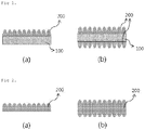
- FIG. 1 light loss may occur at the interface between the substrate layer 100 and the pattern layer 200, thereby remarkably decreasing transmittance or frequently causing light reflection.
- a conventional pattern transfer process such as a roll-to-roll process may be directly applied even without the use of an additional process, thus forming an non-substrate(substrate-less)-type optical sheet having no substrate layer, as shown in FIG. 2 , in which a nano-scale pattern having a pitch of 50 to 500 nm and an aspect ratio of 1.0 to 5.0 is formed on at least one surface thereof.
- the curable resin composition of the present invention preferably includes 100 parts by weight of a urethane acrylate having a weight average molecular weight of 100 to 30,000 and 75 to 250 parts by weight of a fluorine-containing siloxane-acrylate oligomer having a weight average molecular weight of 100 to 10,000 based on 100 parts by weight of the urethane acrylate.
- individual weight average molecular weights preferably fall in the above ranges, and the weight average molecular weights may be determined using a method of measuring the molecular weight of a polymer such as MALDS (Matrix-Assisted Laser Desorption Ionization Mass Spectrometry) or GPC (Gel Permeation Chromatography).
- MALDS Microx-Assisted Laser Desorption Ionization Mass Spectrometry
- GPC Gel Permeation Chromatography
- the urethane acrylate of the present invention is a main component that is added to impart the durability of an optical sheet, resistance to curling and yellowing, flexibility, and supporting capability as a single layer, and may be used in an amount of 20 to 40 wt% based on the total weight of the curable resin in terms of ensuring the above properties.
- the fluorine-containing siloxane-acrylate oligomer is a main component that participates in a curing reaction, and has a molecular structure in which siloxane-acrylate is substituted with fluorine and thus may play an important role in increasing releasability from the mold after the curing process.
- silicone acrylate having a weight average molecular weight of 900 to 1,500 is used to attain releasability from the mold. Silicone acrylate enables the transfer of a pattern on a micro scale but does not satisfy releasability on a nano scale.
- a fluorine resin may be used to obtain releasability. In this case, the resin tends to remain in the mold and contaminates the mold, making it difficult to attain repeatability.
- an oligomer configured such that siloxane-acrylate is substituted with fluorine is used as a main component, thus attaining both releasability and pattern repeatability.
- the amount of the fluorine-containing siloxane-acrylate oligomer is less than 75 parts by weight based on 100 parts by weight of the urethane acrylate, releasability and a transfer rate may decrease, thus causing pattern clustering.
- the amount thereof is 250 parts by weight or less, releasability may be sufficiently ensured.
- the amount thereof preferably does not exceed 250 parts by weight, taking into consideration the price of fluorine.
- the curable resin composition may further include, based on 100 parts by weight of the urethane acrylate, 60 to 125 parts by weight of a diluent and 10 to 25 parts by weight of a polymerization initiator.
- the diluent may be added to adjust the viscosity of the resin, and is preferably an acrylate-based monomer. Since all of the diluent and the main components contain acrylate-based monomers, the double bond of the vinyl group breaks down and thus radical polymerization occurs and a curing reaction may be easily carried out.
- the amount of the diluent preferably falls in the above range in order to maintain the viscosity of the resin in the range of 100 to 300 cps. If the viscosity of the curable resin composition is less than 100 cps, flowability of the composition may excessively increase during the roll-to-roll imprinting process, thus causing variation in film thickness. On the other hand, if the viscosity thereof exceeds 300 cps, the composition may penetrate into the nanopattern, making it difficult to form a desired pattern.
- the polymerization initiator may be at least one selected from the group consisting of a phosphine oxide-based polymerization initiator, a propanone-based polymerization initiator, a ketone-based polymerization initiator and a formate-based polymerization initiator, and is preferably added in an amount of 10 to 25 parts by weight based on 100 parts by weight of the urethane acrylate in order to prevent coloring or deterioration of mechanical strength during the polymerization reaction.
- the curable resin composition of the present invention may further include, but is not necessarily limited to, at least one additive selected from the group consisting of a UV absorbent, a UV stabilizer, a color stabilizer, a leveling agent, an antioxidant, a defoaming agent, and an antistatic agent.
- at least one additive selected from the group consisting of a UV absorbent, a UV stabilizer, a color stabilizer, a leveling agent, an antioxidant, a defoaming agent, and an antistatic agent.
- the optical sheet of the present invention may be manufactured using a roll-to-roll process or a stamp process, and preferably a roll-to-roll process.
- the roll-to-roll process is performed using, as shown in FIGS. 3 to 5 , two guide rolls 11 acting as shafts, a release mold 1, 2 having a nanopattern to form a pattern on an optical sheet, and a slot die 14 for feeding the curable resin composition in the form of a sheet.
- the curable resin composition is fed into a slot die to form a single layer.
- the thickness thereof may be set in the range of 10 to 500 ⁇ m by adjusting the line speed of the roll-to-roll system depending on the end use thereof, but is not necessarily limited thereto.
- the single layer discharged from the slot die may be primarily cured before the formation of the nanopattern, but the present invention is not necessarily limited thereto.
- the pattern of the mold is transferred on one surface or both surfaces of the single layer, thus forming the pattern (S2).
- the pattern may have a micro lens shape in which a hemispherical shape, a cylindrical shape, a trigonal pyramid shape, or a quadrangular pyramid shape is repeated, or a line grid shape, such as a prism or a lenticular pattern, but the present invention is not limited thereto.
- the nanopattern unit shape which is observed on the cross-section when the single layer having the pattern is cut in a vertical direction, preferably has a pitch of 50 to 500 nm and an aspect ratio of 1.0 to 5.0.
- the pattern has a nano size within the above range, thus alleviating changes in refractive index due to the fine irregular structure.
- the formation of the pattern on the single layer in (S2) is preferably carried out in a manner in which the single layer is pre-cured with light at a dose of 50 to 150 mj/cm 2 along with the pattern transfer.
- pre-curing is implemented by irradiating the resin composition with light at a dose of 50 to 150 mj/cm 2 , pattern crushing or layer tearing may be prevented upon release of the pattern from the mold, and curling properties and transmittance of the final optical sheet may be ensured, even without the use of the substrate layer.
- the release mold has to be efficiently released after the transfer of the pattern onto the single layer so as to be repeatedly usable in the roll-to-roll process, and should also be easily washed.
- the release mold may be coated with at least one release agent selected from the group consisting of silicone, fluorine and Teflon.
- the surface of the mold is treated with the release agent in a manner in which the mold body is immersed in the diluted solution of the release agent, or in which the release agent or the diluted solution thereof is applied on the surface of the mold body having the fine irregular structure.
- the immersion of the mold body in the diluted solution of the release agent is more preferably conducted because the surface of the mold body having the fine irregular structure may be uniformly treated with the release agent.
- the single layer having the nanopattern formed in (S2) may be irradiated with light at a dose of 150 mj/cm 2 or more, and preferably 150 to 1,000 mj/cm 2 , thus finally manufacturing an non-substrate(substrate-less)-type optical sheet having a nanopattern (S3).
- the light dose is less than 150 mj/cm 2 , curing is not performed, and reliability may become problematic.
- the light dose exceeds 1,000 mj/cm 2 , brittleness may occur due to over-curing, undesirably causing problems related to handling or reliability.
- the light dose is not necessarily limited thereto, and the light dose and the degree of curing may become optimal taking into account the line speed in the roll-to-roll system upon curing.
- the optical sheet of the present invention may exhibit a transmittance of 95% or more upon irradiation with light at 550 nm and a curl value of 0 mm to 2.0 mm at 23°C.
- the optical sheet has the above optical characteristics and properties, and the present invention is able to provide an non-substrate(substrate-less)-type optical sheet having improved transmittance and stable reliability, compared to optical sheets including a substrate layer.
- a curable resin composition having a viscosity of 150 cps was prepared by mixing, based on the total weight of a mixture, 50 wt% of, as a main compound, a fluorine-containing siloxane-acrylate oligomer having a weight average molecular weight of 5,500, 20 wt% of polyurethane acrylate having a weight average molecular weight of 1,800, 25 wt% of 1,6-hexandiol diacrylate as a diluent and 5 wt% of 1-hydroxy-cyclohexylphenyl-ketone as a polymerization initiator, and was then fed into a roll-to-roll system in which a release mold (available from Soken, Japan) was provided on only one surface of a sheet, as shown in FIG. 3 or 4 , thus manufacturing an non-substrate(substrate-less)-type optical sheet having a nanopattern through the following method.
- An optical sheet having a nanopattern was manufactured in the same manner as in Example 1, with the exception that the same pattern as in Example 1 was formed on both surfaces of the single layer in (S2) (the upper and lower patterns are the same) as shown in FIG. 5 .
- An optical sheet having a nanopattern was manufactured in the same manner as in Example 1, with the exception that the light dose was changed to 50 mj/cm 2 upon pre-curing in (S2).
- An optical sheet having a nanopattern was manufactured in the same manner as in Example 1, with the exception that the light dose was changed to 150 mj/cm 2 upon pre-curing in (S2).
- An optical sheet having a nanopattern was manufactured in the same manner as in Example 1, with the exception that 30 wt% of the fluorine-containing siloxane-acrylate oligomer and 40 wt% of the urethane acrylate were added.
- An optical sheet having a nanopattern with a substrate layer was manufactured in the same manner as in Example 1, with the exception that the same curable composition as in Example 1 was used but a PET film (KOLON, 50 ⁇ m) was used as a substrate layer, and the curable composition was applied to a thickness of 25 ⁇ m on the substrate layer in (S1).
- a PET film KOLON, 50 ⁇ m
- Example 2 The same curable composition as in Example 1 was used, and an attempt was made to omit pre-curing in (S2), but the curable composition became stuck to the mold, making it impossible to manufacture a sheet.
- An optical sheet having a nanopattern was manufactured in the same manner as in Example 1, with the exception that the same curable composition as in Example 1 was used and the light dose was changed to 45 mj/cm 2 upon pre-curing in (S2).
- An optical sheet having a nanopattern was manufactured in the same manner as in Example 1, with the exception that the same curable composition as in Example 1 was used and the light dose was changed to 160 mj/cm 2 upon pre-curing in (S2).
- An non-substrate(substrate-less)-type optical sheet having a nanopattern was manufactured in the same manner as in Example 1, with the exception that 10 wt% of the fluorine-containing siloxane-acrylate oligomer and 60 wt% of the urethane acrylate were added.
- An non-substrate(substrate-less)-type optical sheet having a nanopattern was manufactured in the same manner as in Example 3, with the exception that 30 wt% of polysiloxane acrylate (available from Miwon) having a molecular weight of 1,100 was added in lieu of the fluorine-containing siloxane-acrylate oligomer.
- polysiloxane acrylate available from Miwon
- Comparative Example 7 Formation of non-substrate(substrate-less)-type optical sheet using curable composition having different component and different component ratio
- An non-substrate(substrate-less)-type optical sheet having a nanopattern was manufactured in the same manner as in Example 3, with the exception that 10 wt% of polysiloxane acrylate (available from Miwon) was further added and 30 wt% of the urethane acrylate was added.
- Example 8 Compound A 1) 50 30 10 - 30 - Compound B 2) - - - 30 10 - Compound C 3) 20 40 60 40 30 70 Diluent 4) 25 25 25 25 25 25 25 25 Curing agent 5) 5 5 5 5 5 1)
- the sheet was cut to a size of 5cm*5cm, and the transmittance thereof was measured at a wavelength of 550 nm using a spectrophotometer (CM-3600).
- a sample was subjected to reliability testing under the condition that it was allowed to stand at a temperature of 65°C and a humidity of 85% for 1,000 hr, after which the sample was allowed to stand at room temperature (23°C) for 1 hr, and the curling properties thereof were measured using a steel ruler or a gap gauge.
- the amount of the fluorine-containing siloxane-acrylate oligomer was less than 30 wt% based on the total weight of the composition, as in Comparative Example 5, pattern clustering occurred, thus making it impossible to form a fine nanopattern, thereby significantly decreasing light transmittance.
- Comparative Example 6 using the typical polysiloxane acrylate containing no fluorine in lieu of the fluorine-containing siloxane-acrylate oligomer, releasability was significantly decreased, and thus the nanopattern was not formed.
Landscapes
- Physics & Mathematics (AREA)
- General Physics & Mathematics (AREA)
- Optics & Photonics (AREA)
- Engineering & Computer Science (AREA)
- Mechanical Engineering (AREA)
- Nonlinear Science (AREA)
- Chemical & Material Sciences (AREA)
- Crystallography & Structural Chemistry (AREA)
- Mathematical Physics (AREA)
- Macromonomer-Based Addition Polymer (AREA)
- Moulds For Moulding Plastics Or The Like (AREA)
- Optical Elements Other Than Lenses (AREA)
- Laminated Bodies (AREA)
- Shaping Of Tube Ends By Bending Or Straightening (AREA)
- Liquid Crystal (AREA)
- Surface Treatment Of Optical Elements (AREA)
Abstract
Description
- The present invention relates to an optical sheet for use in a liquid crystal display, and more particularly to an optical sheet having a nanopattern and a method of manufacturing the same.
- Through various studies these days, the case where fine irregular structures having a period equal to or less than that of a visible light wavelength range (about 380 to 780 nm) are formed on the surface of optical devices such as displays, light-emitting diodes, solar cells, etc. is known to exhibit an antireflective effect and a lotus effect to thus increase the efficiency of optical devices. Such a fine irregular structure, which is called a moth-eye structure, plays a role in buffering changes in refractive index between two media having different refractive indexes. Specifically, when light passes through two different media, reflection occurs due to the difference in refractive index, but the refractive indexes of two media are continuously increased in the presence of the fine irregularity between the two media, thus preventing such reflection.
- The formation of a fine irregular structure on the surface of an optical device may include, for example, the method including the following steps of (i) to (iii) (nano-imprinting):
- (i) supplying an active energy ray-curable composition between a mold having a structure complementary to a fine irregular structure and a substrate film, which is the base of a light-transmitting film;
- (ii) forming a cured resin layer having a fine irregular structure on the surface of the substrate film by curing the active energy ray-curable composition through irradiation with an active energy ray such as UV light or the like; and
- (iii) separating the mold from the cured resin layer.
- However, the mold has pores having a period on the nanometer scale and a relatively large aspect ratio, and thus the contact interface between the mold and the active energy ray-curable composition becomes large. Thereby, it is difficult to accurately imprint the pattern of the mold on the cured resin layer, and the separation of the mold in step (iii) becomes very difficult with an increase in the interfacial force. In particular, since the separation of the mold is directly associated with productivity, some patents for solving this problem have been disclosed.
- In this regard,
Japanese Patent Application Publication No. 2007-326367 Japanese Patent Application Publication No. 2009-061628 - Meanwhile, the substrate film on which the cured resin layer having a fine irregular structure is formed is made of PE, PC, PMMA, etc., and such a substrate film has high transparency and flexibility but is disadvantageous in that it is prone to wrinkling and curling. Also, properties such as strength and the like may be improved due to the use of the substrate film, but it is difficult to form a thin film, and the reduction in the manufacturing cost is limited.
- Moreover, as shown in
FIG. 1 , a multilayer structure including a substrate film and a cured resin layer is conventionally formed, and thus light transmission loss may occur at the interlayer interface and non-transmitted light may act as a cause of reflection. Therefore, techniques that do not use the substrate layer have been devised, but are merely implemented in a manner in which the substrate film is stripped through chemical treatment after the formation of the resin layer, and a pattern to be formed is limited to a micro scale. - Accordingly, the present invention is intended to provide an non-substrate(substrate-less)-type optical sheet having a nanopattern, in which a conventional pattern transfer process such as a roll-to-roll process or a stamp process is applied but a substrate film is not used and a nanopattern is formed using only a curable resin, whereby light transmission loss (reflection) at the interface with a substrate does not occur and a high transmittance of 95% or more is exhibited.
- A first preferable embodiment of the present invention provides a method of manufacturing an optical sheet, comprising the following steps of (S1) to (S3):
- (S1) forming a single layer by feeding a curable resin composition; (S2) obtaining the single layer having a transferred nanopattern on a surface thereof by passing the single layer formed in (S1) through a release mold having a nanopattern having a pitch of 50 to 500 nm and an aspect ratio of 1.0 to 5.0; and (S3) curing the single layer having the transferred nanopattern obtained in (S2).
- In the first embodiment, the curable resin composition may include 100 parts by weight of a urethane acrylate having a weight average molecular weight of 100 to 30,000 and 75 to 250 parts by weight of a fluorine-containing siloxane-acrylate oligomer having a weight average molecular weight of 100 to 10,000 based on 100 parts by weight of the urethane acrylate. Here, the curable resin composition may further include, based on 100 parts by weight of the urethane acrylate, 60 to 125 parts by weight of a diluent and 10 to 25 parts by weight of a polymerization initiator. Accordingly, the curable resin composition may have a viscosity of 100 to 300 cps.
- Also in the first embodiment, (S2) may include pre-curing the single layer with light at a dose of 50 to 150 mj/cm2 while transferring the nanopattern, and the release mold, which is used to transfer the pattern, may be coated with at least one release agent selected from the group consisting of silicone, fluorine and Teflon.
- In addition, a second preferable embodiment of the present invention provides an optical sheet, which is formed from a curable composition comprising 100 parts by weight of a urethane acrylate having a weight average molecular weight of 100 to 30,000 and 75 to 250 parts by weight of a fluorine-containing siloxane-acrylate oligomer having a weight average molecular weight of 100 to 10,000 based on 100 parts by weight of the urethane acrylate, and which has a plurality of nanopatterns having a pitch of 50 to 500 nm and an aspect ratio of 1.0 to 5.0 on at least one surface thereof.
- In the second embodiment, the optical sheet may have a transmittance of 95% or more, upon irradiation with light at 550 nm, and a curl value of 0 mm to 2.0 mm at 23°C.
- In the second embodiment, the optical sheet may be manufactured by the method according to the first embodiment.
- According to the present invention, an optical sheet is an non-substrate(substrate-less)-type optical sheet that does not use a substrate, and thus does not generate reflection (light loss) due to the difference in refractive index at the interface between a substrate layer and a resin pattern layer, thereby exhibiting a transmittance of 95% or more and simultaneously improving condensing and diffusion properties of light.
- Also, an optical sheet having a monolayer structure can be manufactured using only a curable resin, and can exhibit superior wrinkling and curling properties even after a reliability test under constant temperature and humidity (60°C, RH85%) and high-temperature (120°C) conditions, making it possible to manufacture a highly reliable optical sheet and to form a thin film. Furthermore, a conventional roll-to-roll process can be applied without change, thus ensuring mass production and price competitiveness by virtue of a reduction in the manufacturing cost without the use of a substrate film during the processing.
-
-
FIG. 1 shows cross-sectional views of a typical nanopattern optical sheet including a nanopattern layer on one surface or both surfaces of a substrate layer; -
FIG. 2 shows cross-sectional views of an non-substrate(substrate-less)-type optical sheet having a plurality of nanopatterns formed using a curable resin according to the present invention; -
FIG. 3 is a schematic view showing a roll-to-roll process for forming a pattern on one surface of a single layer (a curable resin) using a release mold (a soft mold) having a nanopattern according to an exemplary embodiment; -
FIG. 4 is a schematic view showing a roll-to-roll process for forming a pattern on one surface of a single layer (a curable resin) using a release mold (a hard mold) having a nanopattern according to another exemplary embodiment; and -
FIG. 5 is a schematic view showing a roll-to-roll process for forming a pattern on both surfaces of a single layer (a curable resin) using a release mold having a nanopattern according to a further exemplary embodiment. -
- 1: release mold (soft mold) 2: release mold (hard mold)
- 11: guide roll 12: press roll
- 13: winding roll 14: slot die
- 100: substrate layer 200: pattern layer
- An aspect of the present invention addresses a method of manufacturing an optical sheet, comprising: (S1) forming a single layer by feeding a curable resin composition; (S2) obtaining the single layer having a transferred nanopattern on a surface thereof by passing the single layer formed in (S1) through a release mold having a nanopattern having a pitch of 50 to 500 nm and an aspect ratio of 1.0 to 5.0; and (S3) curing the single layer having the transferred nanopattern obtained in (S2).
- A conventional optical sheet having a micropattern or a nanopattern is manufactured by coating the upper surface of a substrate film (a substrate layer) made of PET, PC, PMMA, TAC, COC, or COP with a curable resin and then performing patterning (forming a pattern layer). However, as shown in
FIG. 1 , light loss may occur at the interface between thesubstrate layer 100 and thepattern layer 200, thereby remarkably decreasing transmittance or frequently causing light reflection. Furthermore, in order to solve such problems, the fabrication of an optical sheet having a monolayer structure by forming a pattern layer on a substrate layer and then removing the substrate layer has been proposed, but additionally requires the separation of the substrate layer, and thus the fabrication process thereof becomes very difficult, and limitations are imposed on the application of such a fabrication process to actual processing. - Moreover, when a nano-scale pattern is transferred onto the optical sheet, the surface area on which the curable resin comes into contact with the mold increases and the releasability from the mold is somewhat decreased, making it very difficult to form an optical sheet having a nanopattern without the use of the substrate layer as in conventional cases.
- However, in the present invention, a conventional pattern transfer process such as a roll-to-roll process may be directly applied even without the use of an additional process, thus forming an non-substrate(substrate-less)-type optical sheet having no substrate layer, as shown in
FIG. 2 , in which a nano-scale pattern having a pitch of 50 to 500 nm and an aspect ratio of 1.0 to 5.0 is formed on at least one surface thereof. - In order to manufacture an non-substrate(substrate-less)-type optical sheet having a nano-scale pattern according to the present invention using a conventional imprinting process, the curable resin composition of the present invention preferably includes 100 parts by weight of a urethane acrylate having a weight average molecular weight of 100 to 30,000 and 75 to 250 parts by weight of a fluorine-containing siloxane-acrylate oligomer having a weight average molecular weight of 100 to 10,000 based on 100 parts by weight of the urethane acrylate.
- Here, with the goal of preventing the finally manufactured optical sheet having no substrate layer from being excessively brittle or flexible, individual weight average molecular weights preferably fall in the above ranges, and the weight average molecular weights may be determined using a method of measuring the molecular weight of a polymer such as MALDS (Matrix-Assisted Laser Desorption Ionization Mass Spectrometry) or GPC (Gel Permeation Chromatography).
- In particular, the urethane acrylate of the present invention is a main component that is added to impart the durability of an optical sheet, resistance to curling and yellowing, flexibility, and supporting capability as a single layer, and may be used in an amount of 20 to 40 wt% based on the total weight of the curable resin in terms of ensuring the above properties.
- Also in the present invention, the fluorine-containing siloxane-acrylate oligomer is a main component that participates in a curing reaction, and has a molecular structure in which siloxane-acrylate is substituted with fluorine and thus may play an important role in increasing releasability from the mold after the curing process. For a typical optical sheet having a pattern, silicone acrylate having a weight average molecular weight of 900 to 1,500 is used to attain releasability from the mold. Silicone acrylate enables the transfer of a pattern on a micro scale but does not satisfy releasability on a nano scale. Furthermore, a fluorine resin may be used to obtain releasability. In this case, the resin tends to remain in the mold and contaminates the mold, making it difficult to attain repeatability.
- In contrast, in the present invention, an oligomer configured such that siloxane-acrylate is substituted with fluorine is used as a main component, thus attaining both releasability and pattern repeatability. If the amount of the fluorine-containing siloxane-acrylate oligomer is less than 75 parts by weight based on 100 parts by weight of the urethane acrylate, releasability and a transfer rate may decrease, thus causing pattern clustering. On the other hand, when the amount thereof is 250 parts by weight or less, releasability may be sufficiently ensured. Hence, the amount thereof preferably does not exceed 250 parts by weight, taking into consideration the price of fluorine.
- In the present invention, the curable resin composition may further include, based on 100 parts by weight of the urethane acrylate, 60 to 125 parts by weight of a diluent and 10 to 25 parts by weight of a polymerization initiator. In the present invention, the diluent may be added to adjust the viscosity of the resin, and is preferably an acrylate-based monomer. Since all of the diluent and the main components contain acrylate-based monomers, the double bond of the vinyl group breaks down and thus radical polymerization occurs and a curing reaction may be easily carried out.
- Here, the amount of the diluent preferably falls in the above range in order to maintain the viscosity of the resin in the range of 100 to 300 cps. If the viscosity of the curable resin composition is less than 100 cps, flowability of the composition may excessively increase during the roll-to-roll imprinting process, thus causing variation in film thickness. On the other hand, if the viscosity thereof exceeds 300 cps, the composition may penetrate into the nanopattern, making it difficult to form a desired pattern.
- In the present invention, the polymerization initiator may be at least one selected from the group consisting of a phosphine oxide-based polymerization initiator, a propanone-based polymerization initiator, a ketone-based polymerization initiator and a formate-based polymerization initiator, and is preferably added in an amount of 10 to 25 parts by weight based on 100 parts by weight of the urethane acrylate in order to prevent coloring or deterioration of mechanical strength during the polymerization reaction.
- Furthermore, the curable resin composition of the present invention may further include, but is not necessarily limited to, at least one additive selected from the group consisting of a UV absorbent, a UV stabilizer, a color stabilizer, a leveling agent, an antioxidant, a defoaming agent, and an antistatic agent.
- Meanwhile, the optical sheet of the present invention may be manufactured using a roll-to-roll process or a stamp process, and preferably a roll-to-roll process. Here, the roll-to-roll process is performed using, as shown in
FIGS. 3 to 5 , two guide rolls 11 acting as shafts, arelease mold 1, 2 having a nanopattern to form a pattern on an optical sheet, and a slot die 14 for feeding the curable resin composition in the form of a sheet. - In (S1) of the present invention, the curable resin composition is fed into a slot die to form a single layer. When the single layer is formed, the thickness thereof may be set in the range of 10 to 500 µm by adjusting the line speed of the roll-to-roll system depending on the end use thereof, but is not necessarily limited thereto. The single layer discharged from the slot die may be primarily cured before the formation of the nanopattern, but the present invention is not necessarily limited thereto.
- While the single layer formed in (S1) passes through a release mold having a nanopattern (a soft mold: 1 of
FIGS. 3 and 5 , a hard mold: 2 ofFIGS. 4 and 5 ), the pattern of the mold is transferred on one surface or both surfaces of the single layer, thus forming the pattern (S2). Here, the pattern may have a micro lens shape in which a hemispherical shape, a cylindrical shape, a trigonal pyramid shape, or a quadrangular pyramid shape is repeated, or a line grid shape, such as a prism or a lenticular pattern, but the present invention is not limited thereto. The nanopattern unit shape, which is observed on the cross-section when the single layer having the pattern is cut in a vertical direction, preferably has a pitch of 50 to 500 nm and an aspect ratio of 1.0 to 5.0. The pattern has a nano size within the above range, thus alleviating changes in refractive index due to the fine irregular structure. - In the present invention, the formation of the pattern on the single layer in (S2) is preferably carried out in a manner in which the single layer is pre-cured with light at a dose of 50 to 150 mj/cm2 along with the pattern transfer. When pre-curing is implemented by irradiating the resin composition with light at a dose of 50 to 150 mj/cm2, pattern crushing or layer tearing may be prevented upon release of the pattern from the mold, and curling properties and transmittance of the final optical sheet may be ensured, even without the use of the substrate layer. Here, if light is applied at a dose of less than 50 mj/cm2 upon pre-curing, it is difficult to form the pattern without the use of the substrate, or the curling properties of the sheet may deteriorate. On the other hand, if the light dose exceeds 150 mj/cm2, the non-substrate(substrate-less)-type sheet may be formed, but mold releasability and repeatability may decrease.
- Furthermore, in the present invention, the release mold has to be efficiently released after the transfer of the pattern onto the single layer so as to be repeatedly usable in the roll-to-roll process, and should also be easily washed. Thus, according to a preferred aspect of the present invention, the release mold may be coated with at least one release agent selected from the group consisting of silicone, fluorine and Teflon.
- The surface of the mold is treated with the release agent in a manner in which the mold body is immersed in the diluted solution of the release agent, or in which the release agent or the diluted solution thereof is applied on the surface of the mold body having the fine irregular structure. The immersion of the mold body in the diluted solution of the release agent is more preferably conducted because the surface of the mold body having the fine irregular structure may be uniformly treated with the release agent.
- Subsequently, the single layer having the nanopattern formed in (S2) may be irradiated with light at a dose of 150 mj/cm2 or more, and preferably 150 to 1,000 mj/cm2, thus finally manufacturing an non-substrate(substrate-less)-type optical sheet having a nanopattern (S3). Here, if the light dose is less than 150 mj/cm2, curing is not performed, and reliability may become problematic. On the other hand, if the light dose exceeds 1,000 mj/cm2, brittleness may occur due to over-curing, undesirably causing problems related to handling or reliability. The light dose is not necessarily limited thereto, and the light dose and the degree of curing may become optimal taking into account the line speed in the roll-to-roll system upon curing.
- Thereby, the optical sheet of the present invention may exhibit a transmittance of 95% or more upon irradiation with light at 550 nm and a curl value of 0 mm to 2.0 mm at 23°C. The optical sheet has the above optical characteristics and properties, and the present invention is able to provide an non-substrate(substrate-less)-type optical sheet having improved transmittance and stable reliability, compared to optical sheets including a substrate layer.
- A better understanding of the present invention may be obtained through the following examples, which are set forth to illustrate, but are not to be construed as limiting the scope of the present invention.
- A curable resin composition having a viscosity of 150 cps was prepared by mixing, based on the total weight of a mixture, 50 wt% of, as a main compound, a fluorine-containing siloxane-acrylate oligomer having a weight average molecular weight of 5,500, 20 wt% of polyurethane acrylate having a weight average molecular weight of 1,800, 25 wt% of 1,6-hexandiol diacrylate as a diluent and 5 wt% of 1-hydroxy-cyclohexylphenyl-ketone as a polymerization initiator, and was then fed into a roll-to-roll system in which a release mold (available from Soken, Japan) was provided on only one surface of a sheet, as shown in
FIG. 3 or 4 , thus manufacturing an non-substrate(substrate-less)-type optical sheet having a nanopattern through the following method. - (S1): The prepared curable composition was fed into the slot die of the roll-to-roll system, thus forming a single layer having a thickness of 75 µm via the slot die 14.
- (S2): The single layer formed in (S1) was fed into a release
soft mold 1 having a nanoprism pattern having a pitch of 100 nm and an aspect ratio of 3.5, thus forming a moth-eye pattern on one surface of the single layer while transferring the pattern. Also, upon the transfer of the pattern, UV light was applied at a dose of 100 mj/cm2 so that pre-curing was performed. - (S3): The single layer having the pattern formed in (S2) was cured with UV light at a dose of 500 mj/cm2, finally manufacturing an optical sheet having a nanopattern.
- An optical sheet having a nanopattern was manufactured in the same manner as in Example 1, with the exception that the same pattern as in Example 1 was formed on both surfaces of the single layer in (S2) (the upper and lower patterns are the same) as shown in
FIG. 5 . - An optical sheet having a nanopattern was manufactured in the same manner as in Example 1, with the exception that the light dose was changed to 50 mj/cm2 upon pre-curing in (S2).
- An optical sheet having a nanopattern was manufactured in the same manner as in Example 1, with the exception that the light dose was changed to 150 mj/cm2 upon pre-curing in (S2).
- An optical sheet having a nanopattern was manufactured in the same manner as in Example 1, with the exception that 30 wt% of the fluorine-containing siloxane-acrylate oligomer and 40 wt% of the urethane acrylate were added.
- An optical sheet having a nanopattern with a substrate layer was manufactured in the same manner as in Example 1, with the exception that the same curable composition as in Example 1 was used but a PET film (KOLON, 50 µm) was used as a substrate layer, and the curable composition was applied to a thickness of 25 µm on the substrate layer in (S1).
- The same curable composition as in Example 1 was used, and an attempt was made to omit pre-curing in (S2), but the curable composition became stuck to the mold, making it impossible to manufacture a sheet.
- An optical sheet having a nanopattern was manufactured in the same manner as in Example 1, with the exception that the same curable composition as in Example 1 was used and the light dose was changed to 45 mj/cm2 upon pre-curing in (S2).
- An optical sheet having a nanopattern was manufactured in the same manner as in Example 1, with the exception that the same curable composition as in Example 1 was used and the light dose was changed to 160 mj/cm2 upon pre-curing in (S2).
- An non-substrate(substrate-less)-type optical sheet having a nanopattern was manufactured in the same manner as in Example 1, with the exception that 10 wt% of the fluorine-containing siloxane-acrylate oligomer and 60 wt% of the urethane acrylate were added.
- An non-substrate(substrate-less)-type optical sheet having a nanopattern was manufactured in the same manner as in Example 3, with the exception that 30 wt% of polysiloxane acrylate (available from Miwon) having a molecular weight of 1,100 was added in lieu of the fluorine-containing siloxane-acrylate oligomer.
- An non-substrate(substrate-less)-type optical sheet having a nanopattern was manufactured in the same manner as in Example 3, with the exception that 10 wt% of polysiloxane acrylate (available from Miwon) was further added and 30 wt% of the urethane acrylate was added.
- An attempt was made to manufacture an non-substrate(substrate-less)-type optical sheet having a nanopattern in the same manner as in Example 1, with the exception that the fluorine-containing siloxane-acrylate oligomer or the polysiloxane acrylate was not added and only the urethane acrylate was added in an amount of 70 wt%, but the composition became stuck to the mold and the pattern could not be formed.
- The components of the curable compositions used to manufacture the optical sheets of Examples 1 to 5 and Comparative Examples 1 to 8 are summarized in Table 1 below.
[Table 1] Examples 1 to 4 and Comp. Examples 1 to 4 Example 5 Comp. Example 5 Comp. Example 6 Comp. Example 7 Comp. Example 8 Compound A 1) 50 30 10 - 30 - Compound B 2) - - - 30 10 - Compound C 3) 20 40 60 40 30 70 Diluent 4) 25 25 25 25 25 25 Curing agent 5) 5 5 5 5 5 5 1) Compound A: Fluorine-containing siloxane-acrylate oligomer
2) Compound B: Polysiloxane acrylate
3) Compound C: Urethane acrylate
4) Diluent: (1,6-Hexandiol diacrylate)
5) Curing agent: (1-Hydroxy-cyclohexylphenyl-ketone) - Also, in Examples 1 to 5 and Comparative Examples 1 to 8, except for Comparative Example 2(without pre-curing) and Comparative Example 8 (using a typical composition), in which the formation of the pattern itself was impossible, releasability, light transmittance and curling properties were measured through the following methods. The results are shown in Table 2 below.
- For releasability, when transfer was not performed on the prism after removal of the mold or from the mold after patterning, an outer appearance had defects. The case where defects were observed with the naked eye was determined to be NG (Not Good) and the case where the pattern transfer rate was 90% or more after release upon observation with SEM was determined to be good. Upon five consecutive transfers, when the transfer rate of the optical film was maintained at the same level, repeatability was determined to be good, but when the transfer rate was decreased by 20% or more due to the surface contamination of the mold based on the results of five consecutive transfers, repeatability was determined to be poor.
- The sheet was cut to a size of 5cm*5cm, and the transmittance thereof was measured at a wavelength of 550 nm using a spectrophotometer (CM-3600).
- A sample was subjected to reliability testing under the condition that it was allowed to stand at a temperature of 65°C and a humidity of 85% for 1,000 hr, after which the sample was allowed to stand at room temperature (23°C) for 1 hr, and the curling properties thereof were measured using a steel ruler or a gap gauge.
[Table 2] Presence of substrat e layer Pattern formation Transfer rate Repeatability (5 times) Light transmittance (%, 550 nm) Curl (nm) Ex.1 x One surface Good Good 96.5 0.5 or less Ex.2 X Both surfaces Good Good 99.5 0.5 or less Ex.3 X One surface Good Good 96.1 0.5 or less Ex.4 X One surface Good Good 95.7 0.5 or less Ex.5 X One surface Good Good 96.4 0.5 or less C.Ex. 1 ○ One surface Good Good 94.5 2.5 mm C.Ex. 2 The composition was completely stuck to the mold and the formation of the non-substrate(substrate-less)-type sheet was impossible C.Ex. 3 X One surface Good Good 96.1 2.2 mm C.Ex. 4 X One surface Mold releasabilit y X X 95.7 0.5 or less C.Ex. 5 X One surface Poor (pattern clustering) Not measured 90.1 0.5 or less C.Ex. 6 X One surface Poor Not measured Not measured Not measure d C.Ex. 7 X One surface Fair Poor 96.2 0.5 or less C.Ex. 8 The composition was completely stuck to the mold and the formation of the non-substrate(substrate-less)-type sheet was impossible - As is apparent from Table 2, in Examples 1 to 5, all of the transfer rate, repeatability, light transmittance and curling properties were superior, and particularly, light transmittance and curling properties were significantly improved, compared to Comparative Example 1 including the substrate layer. Based on the results of Comparative Examples 3 and 4, when the light dose was less than 50 mj/cm2 upon pre-curing, curling properties became poor. On the other hand, when the light dose exceeded 150 mj/cm2, the non-substrate(substrate-less)-type sheet was manufactured but the mold releasability was poor, thus deteriorating productivity.
- For the curable composition, if the amount of the fluorine-containing siloxane-acrylate oligomer was less than 30 wt% based on the total weight of the composition, as in Comparative Example 5, pattern clustering occurred, thus making it impossible to form a fine nanopattern, thereby significantly decreasing light transmittance. In Comparative Example 6, using the typical polysiloxane acrylate containing no fluorine in lieu of the fluorine-containing siloxane-acrylate oligomer, releasability was significantly decreased, and thus the nanopattern was not formed. Even when the fluorine-containing siloxane-acrylate oligomer was added in an amount of 30 wt% or more in Comparative Example 7, it was used in a mixture with the polysiloxane acrylate and thus transfer was somewhat possible, but the fluorine content was relatively low, and thus repeatability was low, thereby making it unsuitable for use in mass production.
Claims (10)
- A method of manufacturing an optical sheet, comprising:(S1) forming a single layer by feeding a curable resin composition;(S2) obtaining the single layer having a transferred nanopattern on a surface thereof by passing the single layer formed in (S1) through a release mold having a nanopattern having a pitch of 50 to 500 nm and an aspect ratio of 1.0 to 5.0; and(S3) curing the single layer having the transferred nanopattern obtained in (S2).
- The method of claim 1, wherein the curable resin composition in (S1) comprises 100 parts by weight of a urethane acrylate having a weight average molecular weight of 100 to 30,000 and 75 to 250 parts by weight of a fluorine-containing siloxane-acrylate oligomer having a weight average molecular weight of 100 to 10,000 based on 100 parts by weight of the urethane acrylate.
- The method of claim 2, wherein the curable resin composition in (S1) further comprises, based on 100 parts by weight of the urethane acrylate, 60 to 125 parts by weight of a diluent and 10 to 25 parts by weight of a polymerization initiator.
- The method of claim 1, wherein the curable resin composition in (S1) has a viscosity of 100 to 300 cps.
- The method of claim 1, wherein (S2) comprises pre-curing the single layer with light at a dose of 50 to 150 mj/cm2 while transferring the nanopattern.
- The method of claim 1, wherein the release mold is coated with at least one release agent selected from the group consisting of silicone, fluorine and Teflon.
- An optical sheet, which is formed from a curable composition comprising 100 parts by weight of a urethane acrylate having a weight average molecular weight of 100 to 30,000 and 75 to 250 parts by weight of a fluorine-containing siloxane-acrylate oligomer having a weight average molecular weight of 100 to 10,000 based on 100 parts by weight of the urethane acrylate, and which has a plurality of nanopatterns having a pitch of 50 to 500 nm and an aspect ratio of 1.0 to 5.0 on at least one surface thereof.
- The optical sheet of claim 7, wherein the optical sheet has a transmittance of 95% or more upon irradiation with light at 550 nm.
- The optical sheet of claim 7, wherein the optical sheet has a curl value of 0 to 2.0 mm at 23°C.
- The optical sheet of claim 7, wherein the optical sheet is manufactured by the method of any one of claims 1 to 6.
Applications Claiming Priority (3)
| Application Number | Priority Date | Filing Date | Title |
|---|---|---|---|
| KR20140128162 | 2014-09-25 | ||
| KR1020150134921A KR101776065B1 (en) | 2014-09-25 | 2015-09-23 | Nano Patterned Optical Sheet And Method For Manufacturing The Same |
| PCT/KR2015/010207 WO2016048091A1 (en) | 2014-09-25 | 2015-09-25 | Optical sheet comprising nanopattern and method for manufacturing same |
Publications (3)
| Publication Number | Publication Date |
|---|---|
| EP3199983A1 true EP3199983A1 (en) | 2017-08-02 |
| EP3199983A4 EP3199983A4 (en) | 2018-05-02 |
| EP3199983B1 EP3199983B1 (en) | 2020-01-01 |
Family
ID=55799792
Family Applications (1)
| Application Number | Title | Priority Date | Filing Date |
|---|---|---|---|
| EP15844402.6A Active EP3199983B1 (en) | 2014-09-25 | 2015-09-25 | Optical sheet comprising nanopattern and method for manufacturing same |
Country Status (5)
| Country | Link |
|---|---|
| US (1) | US10132962B2 (en) |
| EP (1) | EP3199983B1 (en) |
| JP (1) | JP6442602B2 (en) |
| KR (1) | KR101776065B1 (en) |
| CN (1) | CN106716183B (en) |
Families Citing this family (2)
| Publication number | Priority date | Publication date | Assignee | Title |
|---|---|---|---|---|
| KR20170079671A (en) * | 2015-12-30 | 2017-07-10 | 코오롱인더스트리 주식회사 | Wire Grid Polarizer And Liquid Crystal Display Device Including The Same |
| KR102547363B1 (en) * | 2023-02-07 | 2023-06-22 | 문제희 | Non-substrate double pattern film and its manufacturing method |
Family Cites Families (19)
| Publication number | Priority date | Publication date | Assignee | Title |
|---|---|---|---|---|
| US20070204953A1 (en) | 2006-02-21 | 2007-09-06 | Ching-Bin Lin | Method for forming structured film as molded by tape die |
| US7854864B2 (en) | 2006-04-28 | 2010-12-21 | Konica Minolta Opto, Inc. | Method for manufacturing an optical film having a convexoconcave structure |
| KR20080014429A (en) | 2006-08-11 | 2008-02-14 | 삼성전자주식회사 | Imprint method |
| KR101457254B1 (en) | 2007-09-28 | 2014-10-31 | 아사히 가라스 가부시키가이샤 | Photocurable composition, method for producing fine patterned body, and optical device |
| KR20090084340A (en) | 2008-02-01 | 2009-08-05 | 주식회사 동진쎄미켐 | Photocurable resin composition and method for preparing of mold using the same |
| JP5306903B2 (en) * | 2008-07-02 | 2013-10-02 | 富士フイルム株式会社 | Curable composition for imprint, cured product using the same, method for producing the same, and member for liquid crystal display device |
| JP5175672B2 (en) * | 2008-09-26 | 2013-04-03 | 富士フイルム株式会社 | Antiglare film, antireflection film, polarizing plate and image display device |
| JP2010186979A (en) * | 2008-12-03 | 2010-08-26 | Fujifilm Corp | Curable composition for imprints, patterning method, and pattern |
| EP2428825B1 (en) * | 2009-06-12 | 2016-05-11 | Sharp Kabushiki Kaisha | Antireflection film, display device and light transmissive member |
| KR101653626B1 (en) | 2009-07-13 | 2016-09-02 | 주식회사 동진쎄미켐 | Photocurable fluoro resin composition and method for preparing of mold using the same |
| JP2012204584A (en) * | 2011-03-25 | 2012-10-22 | Fujifilm Corp | Nanoimprint method |
| EP2744857B1 (en) | 2011-08-17 | 2016-04-27 | 3M Innovative Properties Company | Nanostructured articles and methods to make the same |
| KR101189198B1 (en) * | 2011-08-26 | 2012-10-09 | 주식회사 엘지화학 | Method for manufacturing anti-reflective coating film |
| JP5976523B2 (en) * | 2011-12-28 | 2016-08-23 | 富士フイルム株式会社 | Optical member set and solid-state imaging device using the same |
| KR101698256B1 (en) * | 2012-03-12 | 2017-01-19 | 아사히 가세이 이-매터리얼즈 가부시키가이샤 | Mold, resist laminate and manufacturing process therefor, and microrelief structure |
| WO2013141251A1 (en) | 2012-03-23 | 2013-09-26 | リンテック株式会社 | Film, sheet substrate for processing workpiece, and sheet for processing workpiece |
| JP2013254130A (en) * | 2012-06-08 | 2013-12-19 | Dexerials Corp | Optical element and manufacturing method of the same, display element, and projection type image display device |
| US20150079341A1 (en) * | 2013-09-16 | 2015-03-19 | Tokyo University of Sci. Ed. Foundation Admin. Org | Fabrication method of resin compact, resin compact, and mold |
| JP6186294B2 (en) * | 2014-03-07 | 2017-08-23 | 富士フイルム株式会社 | Antireflection film, polarizing plate, image display device, and production method of antireflection film |
-
2015
- 2015-09-23 KR KR1020150134921A patent/KR101776065B1/en active IP Right Grant
- 2015-09-25 JP JP2017516141A patent/JP6442602B2/en active Active
- 2015-09-25 CN CN201580051845.6A patent/CN106716183B/en not_active Expired - Fee Related
- 2015-09-25 EP EP15844402.6A patent/EP3199983B1/en active Active
- 2015-09-25 US US15/513,345 patent/US10132962B2/en not_active Expired - Fee Related
Also Published As
| Publication number | Publication date |
|---|---|
| US20170299776A1 (en) | 2017-10-19 |
| EP3199983A4 (en) | 2018-05-02 |
| JP6442602B2 (en) | 2018-12-19 |
| CN106716183B (en) | 2018-11-02 |
| JP2017531207A (en) | 2017-10-19 |
| KR20160036508A (en) | 2016-04-04 |
| KR101776065B1 (en) | 2017-09-07 |
| US10132962B2 (en) | 2018-11-20 |
| EP3199983B1 (en) | 2020-01-01 |
| CN106716183A (en) | 2017-05-24 |
Similar Documents
| Publication | Publication Date | Title |
|---|---|---|
| KR101907280B1 (en) | Curable composition for photoimprint and method of producing film, optical component, circuit board, or electronic component using the composition | |
| EP3230796B1 (en) | Poly- or prepolymer composition, or embossing lacquer comprising such a composition and use thereof | |
| US11339288B2 (en) | Photocurable composition and coating layer including cured product thereof | |
| EP2803706A1 (en) | Hard coating composition and decorative film with reduced yellowing comprising same | |
| WO2013005769A1 (en) | Article having fine concavo-convex structure on surface, and image display device provided therewith | |
| EP3199983B1 (en) | Optical sheet comprising nanopattern and method for manufacturing same | |
| JP6906034B2 (en) | Release film with ultra-low release force and its manufacturing method | |
| KR102382953B1 (en) | Multilayered film and method for manufacturing same | |
| KR102453649B1 (en) | Release film for manufacturing ceramic green sheet | |
| US10967563B2 (en) | Method for reducing drawing force in forming process of photocurable material | |
| Almanza-Workman et al. | Fabrication of three-dimensional imprint lithography templates by colloidal dispersions | |
| JP2009167315A (en) | Method for producing porous material | |
| WO2021009980A1 (en) | Photocurable composition, production method for uneven structural body, method for forming minute uneven pattern, and uneven structural body | |
| JP5781464B2 (en) | Method for producing a film with a coating film | |
| JP7180064B2 (en) | Release film for manufacturing ceramic green sheets | |
| JP7262324B2 (en) | Molded article, method for producing molded article, composition, and method for producing composition | |
| JP6442973B2 (en) | Photo-curable composition for microstructure formation and cured product thereof | |
| CN110998380A (en) | Laminated body | |
| JP2019072848A (en) | Release film for ceramic green sheet production | |
| WO2016048091A1 (en) | Optical sheet comprising nanopattern and method for manufacturing same | |
| JP2019055567A (en) | Release film | |
| KR20160037020A (en) | Polyester film for optical use | |
| CN117457509A (en) | Mold release film and method for manufacturing semiconductor package | |
| WO2013191516A1 (en) | Photopolymerisable composition, and optical sheet comprising resin curing layer formed therefrom | |
| KR20160104248A (en) | Anti-glare film, polarizing plate and display device |
Legal Events
| Date | Code | Title | Description |
|---|---|---|---|
| STAA | Information on the status of an ep patent application or granted ep patent |
Free format text: STATUS: THE INTERNATIONAL PUBLICATION HAS BEEN MADE |
|
| PUAI | Public reference made under article 153(3) epc to a published international application that has entered the european phase |
Free format text: ORIGINAL CODE: 0009012 |
|
| STAA | Information on the status of an ep patent application or granted ep patent |
Free format text: STATUS: REQUEST FOR EXAMINATION WAS MADE |
|
| 17P | Request for examination filed |
Effective date: 20170316 |
|
| AK | Designated contracting states |
Kind code of ref document: A1 Designated state(s): AL AT BE BG CH CY CZ DE DK EE ES FI FR GB GR HR HU IE IS IT LI LT LU LV MC MK MT NL NO PL PT RO RS SE SI SK SM TR |
|
| AX | Request for extension of the european patent |
Extension state: BA ME |
|
| DAV | Request for validation of the european patent (deleted) | ||
| DAX | Request for extension of the european patent (deleted) | ||
| REG | Reference to a national code |
Ref country code: DE Ref legal event code: R079 Ref document number: 602015044876 Country of ref document: DE Free format text: PREVIOUS MAIN CLASS: G02B0001110000 Ipc: G02B0001118000 |
|
| A4 | Supplementary search report drawn up and despatched |
Effective date: 20180404 |
|
| RIC1 | Information provided on ipc code assigned before grant |
Ipc: G02F 1/1335 20060101ALI20180327BHEP Ipc: C08J 5/18 20060101ALI20180327BHEP Ipc: G02B 1/118 20150101AFI20180327BHEP |
|
| RAP1 | Party data changed (applicant data changed or rights of an application transferred) |
Owner name: KOLON INDUSTRIES, INC. |
|
| GRAP | Despatch of communication of intention to grant a patent |
Free format text: ORIGINAL CODE: EPIDOSNIGR1 |
|
| STAA | Information on the status of an ep patent application or granted ep patent |
Free format text: STATUS: GRANT OF PATENT IS INTENDED |
|
| INTG | Intention to grant announced |
Effective date: 20190813 |
|
| GRAS | Grant fee paid |
Free format text: ORIGINAL CODE: EPIDOSNIGR3 |
|
| GRAA | (expected) grant |
Free format text: ORIGINAL CODE: 0009210 |
|
| STAA | Information on the status of an ep patent application or granted ep patent |
Free format text: STATUS: THE PATENT HAS BEEN GRANTED |
|
| AK | Designated contracting states |
Kind code of ref document: B1 Designated state(s): AL AT BE BG CH CY CZ DE DK EE ES FI FR GB GR HR HU IE IS IT LI LT LU LV MC MK MT NL NO PL PT RO RS SE SI SK SM TR |
|
| REG | Reference to a national code |
Ref country code: GB Ref legal event code: FG4D |
|
| REG | Reference to a national code |
Ref country code: CH Ref legal event code: EP Ref country code: AT Ref legal event code: REF Ref document number: 1220484 Country of ref document: AT Kind code of ref document: T Effective date: 20200115 |
|
| REG | Reference to a national code |
Ref country code: IE Ref legal event code: FG4D |
|
| REG | Reference to a national code |
Ref country code: DE Ref legal event code: R096 Ref document number: 602015044876 Country of ref document: DE |
|
| REG | Reference to a national code |
Ref country code: NL Ref legal event code: MP Effective date: 20200101 |
|
| REG | Reference to a national code |
Ref country code: LT Ref legal event code: MG4D |
|
| PG25 | Lapsed in a contracting state [announced via postgrant information from national office to epo] |
Ref country code: FI Free format text: LAPSE BECAUSE OF FAILURE TO SUBMIT A TRANSLATION OF THE DESCRIPTION OR TO PAY THE FEE WITHIN THE PRESCRIBED TIME-LIMIT Effective date: 20200101 Ref country code: RS Free format text: LAPSE BECAUSE OF FAILURE TO SUBMIT A TRANSLATION OF THE DESCRIPTION OR TO PAY THE FEE WITHIN THE PRESCRIBED TIME-LIMIT Effective date: 20200101 Ref country code: NO Free format text: LAPSE BECAUSE OF FAILURE TO SUBMIT A TRANSLATION OF THE DESCRIPTION OR TO PAY THE FEE WITHIN THE PRESCRIBED TIME-LIMIT Effective date: 20200401 Ref country code: PT Free format text: LAPSE BECAUSE OF FAILURE TO SUBMIT A TRANSLATION OF THE DESCRIPTION OR TO PAY THE FEE WITHIN THE PRESCRIBED TIME-LIMIT Effective date: 20200527 Ref country code: CZ Free format text: LAPSE BECAUSE OF FAILURE TO SUBMIT A TRANSLATION OF THE DESCRIPTION OR TO PAY THE FEE WITHIN THE PRESCRIBED TIME-LIMIT Effective date: 20200101 Ref country code: NL Free format text: LAPSE BECAUSE OF FAILURE TO SUBMIT A TRANSLATION OF THE DESCRIPTION OR TO PAY THE FEE WITHIN THE PRESCRIBED TIME-LIMIT Effective date: 20200101 Ref country code: LT Free format text: LAPSE BECAUSE OF FAILURE TO SUBMIT A TRANSLATION OF THE DESCRIPTION OR TO PAY THE FEE WITHIN THE PRESCRIBED TIME-LIMIT Effective date: 20200101 |
|
| PG25 | Lapsed in a contracting state [announced via postgrant information from national office to epo] |
Ref country code: IS Free format text: LAPSE BECAUSE OF FAILURE TO SUBMIT A TRANSLATION OF THE DESCRIPTION OR TO PAY THE FEE WITHIN THE PRESCRIBED TIME-LIMIT Effective date: 20200501 Ref country code: BG Free format text: LAPSE BECAUSE OF FAILURE TO SUBMIT A TRANSLATION OF THE DESCRIPTION OR TO PAY THE FEE WITHIN THE PRESCRIBED TIME-LIMIT Effective date: 20200401 Ref country code: HR Free format text: LAPSE BECAUSE OF FAILURE TO SUBMIT A TRANSLATION OF THE DESCRIPTION OR TO PAY THE FEE WITHIN THE PRESCRIBED TIME-LIMIT Effective date: 20200101 Ref country code: SE Free format text: LAPSE BECAUSE OF FAILURE TO SUBMIT A TRANSLATION OF THE DESCRIPTION OR TO PAY THE FEE WITHIN THE PRESCRIBED TIME-LIMIT Effective date: 20200101 Ref country code: LV Free format text: LAPSE BECAUSE OF FAILURE TO SUBMIT A TRANSLATION OF THE DESCRIPTION OR TO PAY THE FEE WITHIN THE PRESCRIBED TIME-LIMIT Effective date: 20200101 Ref country code: GR Free format text: LAPSE BECAUSE OF FAILURE TO SUBMIT A TRANSLATION OF THE DESCRIPTION OR TO PAY THE FEE WITHIN THE PRESCRIBED TIME-LIMIT Effective date: 20200402 |
|
| REG | Reference to a national code |
Ref country code: DE Ref legal event code: R097 Ref document number: 602015044876 Country of ref document: DE |
|
| PG25 | Lapsed in a contracting state [announced via postgrant information from national office to epo] |
Ref country code: EE Free format text: LAPSE BECAUSE OF FAILURE TO SUBMIT A TRANSLATION OF THE DESCRIPTION OR TO PAY THE FEE WITHIN THE PRESCRIBED TIME-LIMIT Effective date: 20200101 Ref country code: DK Free format text: LAPSE BECAUSE OF FAILURE TO SUBMIT A TRANSLATION OF THE DESCRIPTION OR TO PAY THE FEE WITHIN THE PRESCRIBED TIME-LIMIT Effective date: 20200101 Ref country code: SK Free format text: LAPSE BECAUSE OF FAILURE TO SUBMIT A TRANSLATION OF THE DESCRIPTION OR TO PAY THE FEE WITHIN THE PRESCRIBED TIME-LIMIT Effective date: 20200101 Ref country code: ES Free format text: LAPSE BECAUSE OF FAILURE TO SUBMIT A TRANSLATION OF THE DESCRIPTION OR TO PAY THE FEE WITHIN THE PRESCRIBED TIME-LIMIT Effective date: 20200101 Ref country code: SM Free format text: LAPSE BECAUSE OF FAILURE TO SUBMIT A TRANSLATION OF THE DESCRIPTION OR TO PAY THE FEE WITHIN THE PRESCRIBED TIME-LIMIT Effective date: 20200101 Ref country code: RO Free format text: LAPSE BECAUSE OF FAILURE TO SUBMIT A TRANSLATION OF THE DESCRIPTION OR TO PAY THE FEE WITHIN THE PRESCRIBED TIME-LIMIT Effective date: 20200101 |
|
| PLBE | No opposition filed within time limit |
Free format text: ORIGINAL CODE: 0009261 |
|
| STAA | Information on the status of an ep patent application or granted ep patent |
Free format text: STATUS: NO OPPOSITION FILED WITHIN TIME LIMIT |
|
| REG | Reference to a national code |
Ref country code: AT Ref legal event code: MK05 Ref document number: 1220484 Country of ref document: AT Kind code of ref document: T Effective date: 20200101 |
|
| 26N | No opposition filed |
Effective date: 20201002 |
|
| PG25 | Lapsed in a contracting state [announced via postgrant information from national office to epo] |
Ref country code: IT Free format text: LAPSE BECAUSE OF FAILURE TO SUBMIT A TRANSLATION OF THE DESCRIPTION OR TO PAY THE FEE WITHIN THE PRESCRIBED TIME-LIMIT Effective date: 20200101 Ref country code: AT Free format text: LAPSE BECAUSE OF FAILURE TO SUBMIT A TRANSLATION OF THE DESCRIPTION OR TO PAY THE FEE WITHIN THE PRESCRIBED TIME-LIMIT Effective date: 20200101 |
|
| PG25 | Lapsed in a contracting state [announced via postgrant information from national office to epo] |
Ref country code: SI Free format text: LAPSE BECAUSE OF FAILURE TO SUBMIT A TRANSLATION OF THE DESCRIPTION OR TO PAY THE FEE WITHIN THE PRESCRIBED TIME-LIMIT Effective date: 20200101 Ref country code: PL Free format text: LAPSE BECAUSE OF FAILURE TO SUBMIT A TRANSLATION OF THE DESCRIPTION OR TO PAY THE FEE WITHIN THE PRESCRIBED TIME-LIMIT Effective date: 20200101 |
|
| REG | Reference to a national code |
Ref country code: DE Ref legal event code: R119 Ref document number: 602015044876 Country of ref document: DE |
|
| PG25 | Lapsed in a contracting state [announced via postgrant information from national office to epo] |
Ref country code: MC Free format text: LAPSE BECAUSE OF FAILURE TO SUBMIT A TRANSLATION OF THE DESCRIPTION OR TO PAY THE FEE WITHIN THE PRESCRIBED TIME-LIMIT Effective date: 20200101 |
|
| REG | Reference to a national code |
Ref country code: CH Ref legal event code: PL |
|
| GBPC | Gb: european patent ceased through non-payment of renewal fee |
Effective date: 20200925 |
|
| REG | Reference to a national code |
Ref country code: BE Ref legal event code: MM Effective date: 20200930 |
|
| PG25 | Lapsed in a contracting state [announced via postgrant information from national office to epo] |
Ref country code: LU Free format text: LAPSE BECAUSE OF NON-PAYMENT OF DUE FEES Effective date: 20200925 |
|
| PG25 | Lapsed in a contracting state [announced via postgrant information from national office to epo] |
Ref country code: FR Free format text: LAPSE BECAUSE OF NON-PAYMENT OF DUE FEES Effective date: 20200930 Ref country code: DE Free format text: LAPSE BECAUSE OF NON-PAYMENT OF DUE FEES Effective date: 20210401 |
|
| PG25 | Lapsed in a contracting state [announced via postgrant information from national office to epo] |
Ref country code: GB Free format text: LAPSE BECAUSE OF NON-PAYMENT OF DUE FEES Effective date: 20200925 Ref country code: LI Free format text: LAPSE BECAUSE OF NON-PAYMENT OF DUE FEES Effective date: 20200930 Ref country code: IE Free format text: LAPSE BECAUSE OF NON-PAYMENT OF DUE FEES Effective date: 20200925 Ref country code: CH Free format text: LAPSE BECAUSE OF NON-PAYMENT OF DUE FEES Effective date: 20200930 Ref country code: BE Free format text: LAPSE BECAUSE OF NON-PAYMENT OF DUE FEES Effective date: 20200930 |
|
| PG25 | Lapsed in a contracting state [announced via postgrant information from national office to epo] |
Ref country code: TR Free format text: LAPSE BECAUSE OF FAILURE TO SUBMIT A TRANSLATION OF THE DESCRIPTION OR TO PAY THE FEE WITHIN THE PRESCRIBED TIME-LIMIT Effective date: 20200101 Ref country code: MT Free format text: LAPSE BECAUSE OF FAILURE TO SUBMIT A TRANSLATION OF THE DESCRIPTION OR TO PAY THE FEE WITHIN THE PRESCRIBED TIME-LIMIT Effective date: 20200101 Ref country code: CY Free format text: LAPSE BECAUSE OF FAILURE TO SUBMIT A TRANSLATION OF THE DESCRIPTION OR TO PAY THE FEE WITHIN THE PRESCRIBED TIME-LIMIT Effective date: 20200101 |
|
| PG25 | Lapsed in a contracting state [announced via postgrant information from national office to epo] |
Ref country code: MK Free format text: LAPSE BECAUSE OF FAILURE TO SUBMIT A TRANSLATION OF THE DESCRIPTION OR TO PAY THE FEE WITHIN THE PRESCRIBED TIME-LIMIT Effective date: 20200101 Ref country code: AL Free format text: LAPSE BECAUSE OF FAILURE TO SUBMIT A TRANSLATION OF THE DESCRIPTION OR TO PAY THE FEE WITHIN THE PRESCRIBED TIME-LIMIT Effective date: 20200101 |