EP3197601B1 - Taped interlayer flow-cell with metallic masking layers - Google Patents
Taped interlayer flow-cell with metallic masking layers Download PDFInfo
- Publication number
- EP3197601B1 EP3197601B1 EP14902533.0A EP14902533A EP3197601B1 EP 3197601 B1 EP3197601 B1 EP 3197601B1 EP 14902533 A EP14902533 A EP 14902533A EP 3197601 B1 EP3197601 B1 EP 3197601B1
- Authority
- EP
- European Patent Office
- Prior art keywords
- substrate
- masking layer
- double
- sided tape
- taped
- Prior art date
- Legal status (The legal status is an assumption and is not a legal conclusion. Google has not performed a legal analysis and makes no representation as to the accuracy of the status listed.)
- Active
Links
- 239000010410 layer Substances 0.000 title claims description 111
- 230000000873 masking effect Effects 0.000 title claims description 26
- 239000011229 interlayer Substances 0.000 title claims description 14
- 239000000758 substrate Substances 0.000 claims description 86
- 229910052751 metal Inorganic materials 0.000 claims description 47
- 239000002184 metal Substances 0.000 claims description 47
- 230000013011 mating Effects 0.000 claims description 23
- 239000000853 adhesive Substances 0.000 claims description 10
- 230000001070 adhesive effect Effects 0.000 claims description 10
- 239000012790 adhesive layer Substances 0.000 claims description 5
- 239000012876 carrier material Substances 0.000 claims description 5
- XUIMIQQOPSSXEZ-UHFFFAOYSA-N Silicon Chemical compound [Si] XUIMIQQOPSSXEZ-UHFFFAOYSA-N 0.000 claims description 4
- 239000010703 silicon Substances 0.000 claims description 4
- 229910052710 silicon Inorganic materials 0.000 claims description 4
- 239000004020 conductor Substances 0.000 claims description 3
- 239000004642 Polyimide Substances 0.000 claims description 2
- 239000003522 acrylic cement Substances 0.000 claims description 2
- 238000009413 insulation Methods 0.000 claims description 2
- 229920000728 polyester Polymers 0.000 claims description 2
- 229920001721 polyimide Polymers 0.000 claims description 2
- 239000004800 polyvinyl chloride Substances 0.000 claims 1
- 239000013464 silicone adhesive Substances 0.000 claims 1
- 238000000034 method Methods 0.000 description 16
- 238000012545 processing Methods 0.000 description 12
- 238000004519 manufacturing process Methods 0.000 description 7
- 238000005520 cutting process Methods 0.000 description 5
- 239000000463 material Substances 0.000 description 5
- 239000004033 plastic Substances 0.000 description 5
- 229920003023 plastic Polymers 0.000 description 5
- 238000005530 etching Methods 0.000 description 4
- 239000011521 glass Substances 0.000 description 4
- 238000003698 laser cutting Methods 0.000 description 3
- 230000003287 optical effect Effects 0.000 description 3
- 229920001296 polysiloxane Polymers 0.000 description 3
- 238000007789 sealing Methods 0.000 description 3
- 239000004065 semiconductor Substances 0.000 description 3
- 238000013519 translation Methods 0.000 description 3
- 230000015572 biosynthetic process Effects 0.000 description 2
- 239000000919 ceramic Substances 0.000 description 2
- 230000006835 compression Effects 0.000 description 2
- 238000007906 compression Methods 0.000 description 2
- 239000012809 cooling fluid Substances 0.000 description 2
- 238000000151 deposition Methods 0.000 description 2
- 230000008021 deposition Effects 0.000 description 2
- 239000004205 dimethyl polysiloxane Substances 0.000 description 2
- 238000005259 measurement Methods 0.000 description 2
- 238000012986 modification Methods 0.000 description 2
- 230000004048 modification Effects 0.000 description 2
- 229920000435 poly(dimethylsiloxane) Polymers 0.000 description 2
- 230000008569 process Effects 0.000 description 2
- VYZAMTAEIAYCRO-UHFFFAOYSA-N Chromium Chemical compound [Cr] VYZAMTAEIAYCRO-UHFFFAOYSA-N 0.000 description 1
- 229920004943 Delrin® Polymers 0.000 description 1
- NIXOWILDQLNWCW-UHFFFAOYSA-N acrylic acid group Chemical group C(C=C)(=O)O NIXOWILDQLNWCW-UHFFFAOYSA-N 0.000 description 1
- 229910052782 aluminium Inorganic materials 0.000 description 1
- XAGFODPZIPBFFR-UHFFFAOYSA-N aluminium Chemical compound [Al] XAGFODPZIPBFFR-UHFFFAOYSA-N 0.000 description 1
- 238000013459 approach Methods 0.000 description 1
- 238000010420 art technique Methods 0.000 description 1
- 238000005842 biochemical reaction Methods 0.000 description 1
- 238000006243 chemical reaction Methods 0.000 description 1
- 239000003153 chemical reaction reagent Substances 0.000 description 1
- 229910052804 chromium Inorganic materials 0.000 description 1
- 239000011651 chromium Substances 0.000 description 1
- 238000000576 coating method Methods 0.000 description 1
- 230000001419 dependent effect Effects 0.000 description 1
- 238000009792 diffusion process Methods 0.000 description 1
- 238000004049 embossing Methods 0.000 description 1
- 238000005538 encapsulation Methods 0.000 description 1
- 239000012530 fluid Substances 0.000 description 1
- 238000003780 insertion Methods 0.000 description 1
- 230000037431 insertion Effects 0.000 description 1
- 238000000608 laser ablation Methods 0.000 description 1
- 230000007246 mechanism Effects 0.000 description 1
- 238000001465 metallisation Methods 0.000 description 1
- 150000002739 metals Chemical class 0.000 description 1
- 238000004377 microelectronic Methods 0.000 description 1
- 238000012544 monitoring process Methods 0.000 description 1
- 238000000465 moulding Methods 0.000 description 1
- 238000000206 photolithography Methods 0.000 description 1
- 229920003223 poly(pyromellitimide-1,4-diphenyl ether) Polymers 0.000 description 1
- -1 polydimethylsiloxane Polymers 0.000 description 1
- 229920000642 polymer Polymers 0.000 description 1
- 229920002635 polyurethane Polymers 0.000 description 1
- 239000004814 polyurethane Substances 0.000 description 1
- 230000004044 response Effects 0.000 description 1
- 238000000926 separation method Methods 0.000 description 1
- 238000012163 sequencing technique Methods 0.000 description 1
- 238000007493 shaping process Methods 0.000 description 1
- 229910001220 stainless steel Inorganic materials 0.000 description 1
- 239000010935 stainless steel Substances 0.000 description 1
- 239000000126 substance Substances 0.000 description 1
- 238000006467 substitution reaction Methods 0.000 description 1
- 239000012780 transparent material Substances 0.000 description 1
- 230000000007 visual effect Effects 0.000 description 1
- 230000004382 visual function Effects 0.000 description 1
- 239000002699 waste material Substances 0.000 description 1
Images


Classifications
-
- B—PERFORMING OPERATIONS; TRANSPORTING
- B01—PHYSICAL OR CHEMICAL PROCESSES OR APPARATUS IN GENERAL
- B01L—CHEMICAL OR PHYSICAL LABORATORY APPARATUS FOR GENERAL USE
- B01L3/00—Containers or dishes for laboratory use, e.g. laboratory glassware; Droppers
- B01L3/50—Containers for the purpose of retaining a material to be analysed, e.g. test tubes
- B01L3/502—Containers for the purpose of retaining a material to be analysed, e.g. test tubes with fluid transport, e.g. in multi-compartment structures
- B01L3/5027—Containers for the purpose of retaining a material to be analysed, e.g. test tubes with fluid transport, e.g. in multi-compartment structures by integrated microfluidic structures, i.e. dimensions of channels and chambers are such that surface tension forces are important, e.g. lab-on-a-chip
- B01L3/502707—Containers for the purpose of retaining a material to be analysed, e.g. test tubes with fluid transport, e.g. in multi-compartment structures by integrated microfluidic structures, i.e. dimensions of channels and chambers are such that surface tension forces are important, e.g. lab-on-a-chip characterised by the manufacture of the container or its components
-
- B—PERFORMING OPERATIONS; TRANSPORTING
- B32—LAYERED PRODUCTS
- B32B—LAYERED PRODUCTS, i.e. PRODUCTS BUILT-UP OF STRATA OF FLAT OR NON-FLAT, e.g. CELLULAR OR HONEYCOMB, FORM
- B32B15/00—Layered products comprising a layer of metal
- B32B15/04—Layered products comprising a layer of metal comprising metal as the main or only constituent of a layer, which is next to another layer of the same or of a different material
- B32B15/08—Layered products comprising a layer of metal comprising metal as the main or only constituent of a layer, which is next to another layer of the same or of a different material of synthetic resin
-
- B—PERFORMING OPERATIONS; TRANSPORTING
- B32—LAYERED PRODUCTS
- B32B—LAYERED PRODUCTS, i.e. PRODUCTS BUILT-UP OF STRATA OF FLAT OR NON-FLAT, e.g. CELLULAR OR HONEYCOMB, FORM
- B32B15/00—Layered products comprising a layer of metal
- B32B15/18—Layered products comprising a layer of metal comprising iron or steel
-
- B—PERFORMING OPERATIONS; TRANSPORTING
- B32—LAYERED PRODUCTS
- B32B—LAYERED PRODUCTS, i.e. PRODUCTS BUILT-UP OF STRATA OF FLAT OR NON-FLAT, e.g. CELLULAR OR HONEYCOMB, FORM
- B32B15/00—Layered products comprising a layer of metal
- B32B15/20—Layered products comprising a layer of metal comprising aluminium or copper
-
- B—PERFORMING OPERATIONS; TRANSPORTING
- B32—LAYERED PRODUCTS
- B32B—LAYERED PRODUCTS, i.e. PRODUCTS BUILT-UP OF STRATA OF FLAT OR NON-FLAT, e.g. CELLULAR OR HONEYCOMB, FORM
- B32B27/00—Layered products comprising a layer of synthetic resin
- B32B27/06—Layered products comprising a layer of synthetic resin as the main or only constituent of a layer, which is next to another layer of the same or of a different material
- B32B27/08—Layered products comprising a layer of synthetic resin as the main or only constituent of a layer, which is next to another layer of the same or of a different material of synthetic resin
-
- B—PERFORMING OPERATIONS; TRANSPORTING
- B32—LAYERED PRODUCTS
- B32B—LAYERED PRODUCTS, i.e. PRODUCTS BUILT-UP OF STRATA OF FLAT OR NON-FLAT, e.g. CELLULAR OR HONEYCOMB, FORM
- B32B27/00—Layered products comprising a layer of synthetic resin
- B32B27/28—Layered products comprising a layer of synthetic resin comprising synthetic resins not wholly covered by any one of the sub-groups B32B27/30 - B32B27/42
- B32B27/281—Layered products comprising a layer of synthetic resin comprising synthetic resins not wholly covered by any one of the sub-groups B32B27/30 - B32B27/42 comprising polyimides
-
- B—PERFORMING OPERATIONS; TRANSPORTING
- B32—LAYERED PRODUCTS
- B32B—LAYERED PRODUCTS, i.e. PRODUCTS BUILT-UP OF STRATA OF FLAT OR NON-FLAT, e.g. CELLULAR OR HONEYCOMB, FORM
- B32B27/00—Layered products comprising a layer of synthetic resin
- B32B27/28—Layered products comprising a layer of synthetic resin comprising synthetic resins not wholly covered by any one of the sub-groups B32B27/30 - B32B27/42
- B32B27/285—Layered products comprising a layer of synthetic resin comprising synthetic resins not wholly covered by any one of the sub-groups B32B27/30 - B32B27/42 comprising polyethers
-
- B—PERFORMING OPERATIONS; TRANSPORTING
- B32—LAYERED PRODUCTS
- B32B—LAYERED PRODUCTS, i.e. PRODUCTS BUILT-UP OF STRATA OF FLAT OR NON-FLAT, e.g. CELLULAR OR HONEYCOMB, FORM
- B32B27/00—Layered products comprising a layer of synthetic resin
- B32B27/30—Layered products comprising a layer of synthetic resin comprising vinyl (co)polymers; comprising acrylic (co)polymers
- B32B27/304—Layered products comprising a layer of synthetic resin comprising vinyl (co)polymers; comprising acrylic (co)polymers comprising vinyl halide (co)polymers, e.g. PVC, PVDC, PVF, PVDF
-
- B—PERFORMING OPERATIONS; TRANSPORTING
- B32—LAYERED PRODUCTS
- B32B—LAYERED PRODUCTS, i.e. PRODUCTS BUILT-UP OF STRATA OF FLAT OR NON-FLAT, e.g. CELLULAR OR HONEYCOMB, FORM
- B32B27/00—Layered products comprising a layer of synthetic resin
- B32B27/36—Layered products comprising a layer of synthetic resin comprising polyesters
-
- B—PERFORMING OPERATIONS; TRANSPORTING
- B32—LAYERED PRODUCTS
- B32B—LAYERED PRODUCTS, i.e. PRODUCTS BUILT-UP OF STRATA OF FLAT OR NON-FLAT, e.g. CELLULAR OR HONEYCOMB, FORM
- B32B27/00—Layered products comprising a layer of synthetic resin
- B32B27/40—Layered products comprising a layer of synthetic resin comprising polyurethanes
-
- B—PERFORMING OPERATIONS; TRANSPORTING
- B32—LAYERED PRODUCTS
- B32B—LAYERED PRODUCTS, i.e. PRODUCTS BUILT-UP OF STRATA OF FLAT OR NON-FLAT, e.g. CELLULAR OR HONEYCOMB, FORM
- B32B3/00—Layered products comprising a layer with external or internal discontinuities or unevennesses, or a layer of non-planar shape; Layered products comprising a layer having particular features of form
- B32B3/02—Layered products comprising a layer with external or internal discontinuities or unevennesses, or a layer of non-planar shape; Layered products comprising a layer having particular features of form characterised by features of form at particular places, e.g. in edge regions
- B32B3/04—Layered products comprising a layer with external or internal discontinuities or unevennesses, or a layer of non-planar shape; Layered products comprising a layer having particular features of form characterised by features of form at particular places, e.g. in edge regions characterised by at least one layer folded at the edge, e.g. over another layer ; characterised by at least one layer enveloping or enclosing a material
-
- B—PERFORMING OPERATIONS; TRANSPORTING
- B32—LAYERED PRODUCTS
- B32B—LAYERED PRODUCTS, i.e. PRODUCTS BUILT-UP OF STRATA OF FLAT OR NON-FLAT, e.g. CELLULAR OR HONEYCOMB, FORM
- B32B3/00—Layered products comprising a layer with external or internal discontinuities or unevennesses, or a layer of non-planar shape; Layered products comprising a layer having particular features of form
- B32B3/26—Layered products comprising a layer with external or internal discontinuities or unevennesses, or a layer of non-planar shape; Layered products comprising a layer having particular features of form characterised by a particular shape of the outline of the cross-section of a continuous layer; characterised by a layer with cavities or internal voids ; characterised by an apertured layer
- B32B3/263—Layered products comprising a layer with external or internal discontinuities or unevennesses, or a layer of non-planar shape; Layered products comprising a layer having particular features of form characterised by a particular shape of the outline of the cross-section of a continuous layer; characterised by a layer with cavities or internal voids ; characterised by an apertured layer characterised by a layer having non-uniform thickness
-
- B—PERFORMING OPERATIONS; TRANSPORTING
- B32—LAYERED PRODUCTS
- B32B—LAYERED PRODUCTS, i.e. PRODUCTS BUILT-UP OF STRATA OF FLAT OR NON-FLAT, e.g. CELLULAR OR HONEYCOMB, FORM
- B32B3/00—Layered products comprising a layer with external or internal discontinuities or unevennesses, or a layer of non-planar shape; Layered products comprising a layer having particular features of form
- B32B3/26—Layered products comprising a layer with external or internal discontinuities or unevennesses, or a layer of non-planar shape; Layered products comprising a layer having particular features of form characterised by a particular shape of the outline of the cross-section of a continuous layer; characterised by a layer with cavities or internal voids ; characterised by an apertured layer
- B32B3/266—Layered products comprising a layer with external or internal discontinuities or unevennesses, or a layer of non-planar shape; Layered products comprising a layer having particular features of form characterised by a particular shape of the outline of the cross-section of a continuous layer; characterised by a layer with cavities or internal voids ; characterised by an apertured layer characterised by an apertured layer, the apertures going through the whole thickness of the layer, e.g. expanded metal, perforated layer, slit layer regular cells B32B3/12
-
- B—PERFORMING OPERATIONS; TRANSPORTING
- B32—LAYERED PRODUCTS
- B32B—LAYERED PRODUCTS, i.e. PRODUCTS BUILT-UP OF STRATA OF FLAT OR NON-FLAT, e.g. CELLULAR OR HONEYCOMB, FORM
- B32B7/00—Layered products characterised by the relation between layers; Layered products characterised by the relative orientation of features between layers, or by the relative values of a measurable parameter between layers, i.e. products comprising layers having different physical, chemical or physicochemical properties; Layered products characterised by the interconnection of layers
- B32B7/04—Interconnection of layers
- B32B7/06—Interconnection of layers permitting easy separation
-
- B—PERFORMING OPERATIONS; TRANSPORTING
- B32—LAYERED PRODUCTS
- B32B—LAYERED PRODUCTS, i.e. PRODUCTS BUILT-UP OF STRATA OF FLAT OR NON-FLAT, e.g. CELLULAR OR HONEYCOMB, FORM
- B32B7/00—Layered products characterised by the relation between layers; Layered products characterised by the relative orientation of features between layers, or by the relative values of a measurable parameter between layers, i.e. products comprising layers having different physical, chemical or physicochemical properties; Layered products characterised by the interconnection of layers
- B32B7/04—Interconnection of layers
- B32B7/12—Interconnection of layers using interposed adhesives or interposed materials with bonding properties
-
- B—PERFORMING OPERATIONS; TRANSPORTING
- B32—LAYERED PRODUCTS
- B32B—LAYERED PRODUCTS, i.e. PRODUCTS BUILT-UP OF STRATA OF FLAT OR NON-FLAT, e.g. CELLULAR OR HONEYCOMB, FORM
- B32B9/00—Layered products comprising a layer of a particular substance not covered by groups B32B11/00 - B32B29/00
- B32B9/005—Layered products comprising a layer of a particular substance not covered by groups B32B11/00 - B32B29/00 comprising one layer of ceramic material, e.g. porcelain, ceramic tile
-
- B—PERFORMING OPERATIONS; TRANSPORTING
- B32—LAYERED PRODUCTS
- B32B—LAYERED PRODUCTS, i.e. PRODUCTS BUILT-UP OF STRATA OF FLAT OR NON-FLAT, e.g. CELLULAR OR HONEYCOMB, FORM
- B32B9/00—Layered products comprising a layer of a particular substance not covered by groups B32B11/00 - B32B29/00
- B32B9/04—Layered products comprising a layer of a particular substance not covered by groups B32B11/00 - B32B29/00 comprising such particular substance as the main or only constituent of a layer, which is next to another layer of the same or of a different material
- B32B9/041—Layered products comprising a layer of a particular substance not covered by groups B32B11/00 - B32B29/00 comprising such particular substance as the main or only constituent of a layer, which is next to another layer of the same or of a different material of metal
-
- B—PERFORMING OPERATIONS; TRANSPORTING
- B32—LAYERED PRODUCTS
- B32B—LAYERED PRODUCTS, i.e. PRODUCTS BUILT-UP OF STRATA OF FLAT OR NON-FLAT, e.g. CELLULAR OR HONEYCOMB, FORM
- B32B9/00—Layered products comprising a layer of a particular substance not covered by groups B32B11/00 - B32B29/00
- B32B9/04—Layered products comprising a layer of a particular substance not covered by groups B32B11/00 - B32B29/00 comprising such particular substance as the main or only constituent of a layer, which is next to another layer of the same or of a different material
- B32B9/045—Layered products comprising a layer of a particular substance not covered by groups B32B11/00 - B32B29/00 comprising such particular substance as the main or only constituent of a layer, which is next to another layer of the same or of a different material of synthetic resin
-
- C—CHEMISTRY; METALLURGY
- C23—COATING METALLIC MATERIAL; COATING MATERIAL WITH METALLIC MATERIAL; CHEMICAL SURFACE TREATMENT; DIFFUSION TREATMENT OF METALLIC MATERIAL; COATING BY VACUUM EVAPORATION, BY SPUTTERING, BY ION IMPLANTATION OR BY CHEMICAL VAPOUR DEPOSITION, IN GENERAL; INHIBITING CORROSION OF METALLIC MATERIAL OR INCRUSTATION IN GENERAL
- C23F—NON-MECHANICAL REMOVAL OF METALLIC MATERIAL FROM SURFACE; INHIBITING CORROSION OF METALLIC MATERIAL OR INCRUSTATION IN GENERAL; MULTI-STEP PROCESSES FOR SURFACE TREATMENT OF METALLIC MATERIAL INVOLVING AT LEAST ONE PROCESS PROVIDED FOR IN CLASS C23 AND AT LEAST ONE PROCESS COVERED BY SUBCLASS C21D OR C22F OR CLASS C25
- C23F1/00—Etching metallic material by chemical means
-
- B—PERFORMING OPERATIONS; TRANSPORTING
- B01—PHYSICAL OR CHEMICAL PROCESSES OR APPARATUS IN GENERAL
- B01L—CHEMICAL OR PHYSICAL LABORATORY APPARATUS FOR GENERAL USE
- B01L2200/00—Solutions for specific problems relating to chemical or physical laboratory apparatus
- B01L2200/12—Specific details about manufacturing devices
-
- B—PERFORMING OPERATIONS; TRANSPORTING
- B01—PHYSICAL OR CHEMICAL PROCESSES OR APPARATUS IN GENERAL
- B01L—CHEMICAL OR PHYSICAL LABORATORY APPARATUS FOR GENERAL USE
- B01L2300/00—Additional constructional details
- B01L2300/06—Auxiliary integrated devices, integrated components
- B01L2300/0627—Sensor or part of a sensor is integrated
- B01L2300/0645—Electrodes
-
- B—PERFORMING OPERATIONS; TRANSPORTING
- B01—PHYSICAL OR CHEMICAL PROCESSES OR APPARATUS IN GENERAL
- B01L—CHEMICAL OR PHYSICAL LABORATORY APPARATUS FOR GENERAL USE
- B01L2300/00—Additional constructional details
- B01L2300/08—Geometry, shape and general structure
- B01L2300/0887—Laminated structure
-
- B—PERFORMING OPERATIONS; TRANSPORTING
- B01—PHYSICAL OR CHEMICAL PROCESSES OR APPARATUS IN GENERAL
- B01L—CHEMICAL OR PHYSICAL LABORATORY APPARATUS FOR GENERAL USE
- B01L2400/00—Moving or stopping fluids
- B01L2400/04—Moving fluids with specific forces or mechanical means
- B01L2400/0403—Moving fluids with specific forces or mechanical means specific forces
- B01L2400/0415—Moving fluids with specific forces or mechanical means specific forces electrical forces, e.g. electrokinetic
-
- B—PERFORMING OPERATIONS; TRANSPORTING
- B32—LAYERED PRODUCTS
- B32B—LAYERED PRODUCTS, i.e. PRODUCTS BUILT-UP OF STRATA OF FLAT OR NON-FLAT, e.g. CELLULAR OR HONEYCOMB, FORM
- B32B2255/00—Coating on the layer surface
-
- B—PERFORMING OPERATIONS; TRANSPORTING
- B32—LAYERED PRODUCTS
- B32B—LAYERED PRODUCTS, i.e. PRODUCTS BUILT-UP OF STRATA OF FLAT OR NON-FLAT, e.g. CELLULAR OR HONEYCOMB, FORM
- B32B2255/00—Coating on the layer surface
- B32B2255/10—Coating on the layer surface on synthetic resin layer or on natural or synthetic rubber layer
-
- B—PERFORMING OPERATIONS; TRANSPORTING
- B32—LAYERED PRODUCTS
- B32B—LAYERED PRODUCTS, i.e. PRODUCTS BUILT-UP OF STRATA OF FLAT OR NON-FLAT, e.g. CELLULAR OR HONEYCOMB, FORM
- B32B2255/00—Coating on the layer surface
- B32B2255/20—Inorganic coating
- B32B2255/205—Metallic coating
-
- B—PERFORMING OPERATIONS; TRANSPORTING
- B32—LAYERED PRODUCTS
- B32B—LAYERED PRODUCTS, i.e. PRODUCTS BUILT-UP OF STRATA OF FLAT OR NON-FLAT, e.g. CELLULAR OR HONEYCOMB, FORM
- B32B2307/00—Properties of the layers or laminate
- B32B2307/40—Properties of the layers or laminate having particular optical properties
- B32B2307/412—Transparent
-
- B—PERFORMING OPERATIONS; TRANSPORTING
- B32—LAYERED PRODUCTS
- B32B—LAYERED PRODUCTS, i.e. PRODUCTS BUILT-UP OF STRATA OF FLAT OR NON-FLAT, e.g. CELLULAR OR HONEYCOMB, FORM
- B32B2307/00—Properties of the layers or laminate
- B32B2307/50—Properties of the layers or laminate having particular mechanical properties
- B32B2307/546—Flexural strength; Flexion stiffness
-
- B—PERFORMING OPERATIONS; TRANSPORTING
- B32—LAYERED PRODUCTS
- B32B—LAYERED PRODUCTS, i.e. PRODUCTS BUILT-UP OF STRATA OF FLAT OR NON-FLAT, e.g. CELLULAR OR HONEYCOMB, FORM
- B32B2307/00—Properties of the layers or laminate
- B32B2307/50—Properties of the layers or laminate having particular mechanical properties
- B32B2307/58—Cuttability
-
- B—PERFORMING OPERATIONS; TRANSPORTING
- B32—LAYERED PRODUCTS
- B32B—LAYERED PRODUCTS, i.e. PRODUCTS BUILT-UP OF STRATA OF FLAT OR NON-FLAT, e.g. CELLULAR OR HONEYCOMB, FORM
- B32B2307/00—Properties of the layers or laminate
- B32B2307/70—Other properties
- B32B2307/748—Releasability
Definitions
- Embodiments of the disclosure relate generally to the field of taped interlayer flow cells and more particularly to a method and structure for producing a taped interlayer flow cell with precision tape geometry and cell assembly including masking of the tape layer and conductive trace formation.
- the invention is defined in claim 1.
- Microfluidic devices often referred to as flow cells, provide very precise means to carry out complicated biochemical reactions to acquire important chemical and biological information.
- microfluidic systems reduce the required number of samples and quantities of reagents employed, shorten the response time of reactions, and decrease the amount of biohazard waste for disposal.
- initial microfluidic devices were fabricated in silicon and glass using photolithography and etching techniques adapted from the microelectronics industry.
- Many current microfluidic devices made using this method of fabrication are constructed from plastic, silicone or other polymeric materials, e.g. polydimethylsiloxane (PDMS).
- PDMS polydimethylsiloxane
- Such devices are generally expensive, inflexible, and difficult to construct.
- Examples of layered microfluidic devices are known from US 2012/052250 A1 , US 2005/023765 A1 , US 2004/154923 A1 , WO 2009/102688 A2 and WO 01/25138 A1 .
- a double-sided tape is used between two transparent substrates, which consists of a carrier material with an adhesive layer on the top and bottom and a removable liner covering the adhesive layers.
- Preferred double-sided tapes for all the embodiments described herein include double-sided silicone tape 3M 96042 or double-sided acrylic/silicone tape 3M 9731, but the choice of tape is dependent on the materials being used.
- Microchannels are created by cutting out parts of the double-sided tape and covering it with a sheet of material--glass is preferable for the base, plastics can alternatively be used as the top or bottom cover. Microchannels can be created in plastics or other materials by embossing, etching, or any structuring method. Any number of microfluidic device components can be included on the tape. These might include, for example, microchannels, microvalves or other pneumatic elements, diffusion chambers, manifolds, holes that connect one layer to another (vias), inlet and outlet ports, and other microfluidic device components.
- a flow cell having a first substrate with a metal layer on one surface.
- a tape layer having flow channels is adhered to the first substrate.
- a second substrate having a second metal layer on one surface is adhered to the tape layer opposite the first substrate.
- the first and second metal layers include mating cutouts to allow viewing of the flow channels.
- the embodiments disclosed provide a method for fabrication of a flow cell wherein a substrate is provided with a deposited metal layer on one surface. A tape layer is adhered to the substrate. The metal layer is etched prior to or after taping or otherwise formed to include mating openings for viewing flow channels. A mating substrate is provided with a second deposited metal layer on one surface. The mating substrate may contain holes that connect to the flow channels. The second metal layer may be etched or otherwise formed to include mating openings for viewing the flow channels. The mating substrate is then aligned with and bonded to the tape layer.
- Embodiments disclosed herein provide methods and apparatus for fabricating a taped interlayer flow cell. None of the prior art use a laser to obtain high precision, have a metallization layer to hide the imperfections in the tape, use a removable tape (UV release), or combine a standard well with a room temperature bonded edges to obtain better channel dimensional properties or a fast customization of the flow cell. Use of UV or thermally releasable tape also allows the flow cell to be easily disassembled, which may be advantageous for certain applications. Also, adding electrical leads to the flow cell is a challenge and normally accomplished with external leads. Finally, the prior art fabrication methods with tape cannot be done on wafer level processing due to issues dicing the components on a wafer containing a tape layer.
- FIG. 1 shows a first embodiment of a flow cell having a first or top substrate 10 with one or more inlet/exit holes 11.
- a metal layer 12 is deposited on an upper or lower surface of the first substrate (a lower surface deposition being shown in FIG. 1 ).
- a tape layer 14 with one or more laser cut flow channels 15 has double sided adhesive to adhere to the metal layer 12 on first and second substrate (to be described subsequently).
- the metal layer 12 has mating cutouts 13 sized to expose the flow channels 15. With the tape layer adhered to the metal layer or, in embodiments with the metal layer on an upper surface of the first substrate, the first substrate, an enclosed flow cell running between the inlet/exit ports 11 is created.
- the tape layer 14 may have a temporary cover layer that can be removed to expose the adhesive as necessary.
- the substrate 10 is transparent to allow viewing of the flow channel through the cutouts 13 in the metal layer 12 and may be also be predominantly transparent to a predetermined wavelength of a laser employed for processing as will be described subsequently, which will prevent excessive heat being generated at the interface.
- a second or bottom substrate 16 has a second metal layer 18 deposited on an upper or lower surface (an upper surface deposition being shown in FIG. 1 ).
- the second metal layer incorporates cutouts 19 sized to expose the flow channels 15 and the substrate 16 is also transparent to allow viewing of the flow channels 15.
- the double sided adhesive on the tape layer 14 adheres to either the metal layer 18 or the substrate 16 depending on the surface on which the metal layer is deposited.
- the first substrate 10 and second substrate 16 may be glass, silicon, ceramic, plastic, or similar transparent materials.
- the metal layers 12, 18 are typically chromium for glass substrates but may employ alternative metals.
- the tape layer 14 is a flexible PVC with synthetic acrylic adhesive bonded to both sides, similar to semiconductor wafer dicing tape supplied by companies like Lintec or Semiconductor Equipment Corporation.
- the tape layer may alternatively be masking tapes made of Kapton polyimide or polyester or have a silicon adhesive
- the flow cell 20 allows viewing of the flow channels through the cutouts in the first and second metal layers.
- the metal layers on the substrates cover the adhesive attachment of the tape layer to the substrates thereby providing aesthetic masking of any imperfections in the adhesive such as bubbles, striations or graininess that would be visible through the transparent substrates.
- the cutouts 13 and 19 may be sized and shaped substantially identically to the flow channels 15 in the tape layer or may be undersized to mask a portion of the flow cell.
- the cutouts may be formed in the metal layers on the substrates prior to assembly of the substrates, or they may be formed after assembly by running an etchant through the completed flow cell channels. Using undersized cut outs or forming the cutouts after assembly eliminates the need for exact alignment of the cut outs to the flow channels. Lateral masking across the flow channels may be employed for process marking or other visual functions associated with the flow cell.
- the metal layers may additionally provide integral electrical conductors for process functions associated with the flow channels as shown in FIGs. 3 and 4 .
- the metal layers 12, 18 may be deposited on the substrates and structured by etching or laser processing to provide the cutouts 13, 19.
- electrical leads 22 may be formed for contact with one or more of the flow channels 15.
- the leads are present in the second metal layer 18 deposited on the second substrate 16.
- the leads 22 may be attached to contact pads 23 for external electrical connection. While two simple leads for one channel are shown in FIG. 3 , multiple leads extending from multiple sides of the flow cell may be provided and conductors etched within the metal layers for isolated interconnection between or around flow channels.
- Cutouts 24 are provided in the tape layer 14, upper metal layer 12 and top substrate 10 to expose the contact pads 23 for electrical connection with external circuitry.
- the tape layer 14 provides insulation between the first metal layer 12 and second metal layer 18 for embodiments in which the metal layers are on interior surfaces of the substrates.
- Processing of the tape layer for creation of the flow channels may be accomplished employing a wafer 25 of the substrate material, which may contain a plurality of individual chips that are later diced into separate units as shown in FIG. 5 .
- a round wafer is employed and tape adhered to the wafer is initially cut leaving a pattern of multiple tape layers 14.
- FIG. 5 is shown with the excess tape removed.
- the wafer 25 is put in a fixture 28 mounted to the x axis and y axis motion stage on a laser bonding machine as disclosed in copending application serial no. 13/291,956 filed on 11/08/2011 entitled ROOM TEMPERATURE GLASS-TO-PLASTIC AND GLASS-TO-CERAMIC/SEMICONDUCTOR BONDING as shown in FIG.
- the fixture 28 can use a vacuum chuck or any comparable means to clamp the substrate work piece.
- a positioning system 30 incorporates an x-axis motion stage 32 mounted on a base 33 and a y-axis motion stage 34 mounted to the x-axis mounting stage.
- a substrate alignment fixture 28 is mounted on the y-axis motion stage.
- the motion stages may be reversed in vertical stacking and the alignment fixture mounted on the x-axis stage.
- Each motion stage has a drive motor 38 with associated screw drive 40 or similar translation mechanism. Covers 42 shield the operating elements of the motion stages for operator safety.
- a gantry 44 provides support for alignment optics 46 for the laser 14, and for a z-motion stage, that carries final focusing optics 48, camera 50 and other instrumentation systems as required for monitoring and controling the bonding operation.
- a power meter 52 is mounted to the x-axis motion stage to be positioned under the laser optical train for measurement and/or calibration of laser power before movement of the alignment fixture under the laser optics for tape cutting.
- a z-axis motion stage 54 is provided for vertical positioning of the optical and measurement systems with respect to the alignment fixture.
- a computer controller 55 is programmable for translation of the x-axis, y-axis and z-axis motion stages for translation of the laser on the work piece.
- a single laser may be employed for illuminating multiple substrate work pieces in individual positioning systems by employing beam splitters and focusing optical trains to the multiple positioning systems. It is also possible to replace the fixed lens with an f-theta lens with an X-Y scanner and Z-auto-focus either by itself or in conjunction with a large travel X-Y positioning system.
- the laser is focused on the tape layer, and the stage is traversed to cut precise flow channels 15.
- the laser may ablate the tape creating the flow channels or the laser may cut an outline of the channels and then the inner portion of the outline is subsequently removed from the substrate.
- a second substrate wafer is then aligned with the first and bonded to the taped side of the first substrate wafer, thereby enclosing or capping the flow cells.
- one or both substrates may have through holes (manufactured by any means) located at precise locations to create inlets and exits of the flow cell.
- the embodiments disclosed allow dicing the tape inner layer flow cells from a wafer containing multiple chips.
- the typical method is using a dicing saw.
- the tape can create a seal with the cutting blade which restricts cooling fluid from flowing into the kerf and causes the blade to overheat.
- the tape can be removed from the dicing lines 26 as shown in FIG. 6 to create individual tape layer masks prior to the dicing operation via laser ablation or laser cutting in a similar fashion used to create the flow channels 15 and at the same time. This leaves a clear path for the dicing saw and cooling fluid.
- the dicing lines may have sufficient width to space the tape layer masks for placement in a well in a substrate as will be described subsequently.
- An additional processing step would be to the pre-dice the wafer prior to application of the tape, and leave small areas (tabs) to hold the wafer together as a monolithic unit.
- tabs small areas
- the small tab areas can be cut with the laser either during or after the tape cutting process thereby eliminating the saw cutting of the completed wafer.
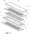
- the tape layer 14 is received inside a well 60 in a bottom substrate 62.
- the well is designed such that the height 63 of the well 60 is a precise dimension that defines the desired height of the flow cell.
- the well height would preferably be slightly less than the thickness of the tape layer 14, such that it provides some compressive force on the tape to improve adhesion and pressure capacity of the flow cell upon assembly as described subsequently.
- the outside edges 64 of the bottom substrate 62 surrounding the well 60 would also provide a flat surface 66 which can be laser bonded to the capping substrate 68 which has length 69a and width 69b sufficient to overlap the edges 64 in the lower substrate 62.
- the flat surface 66 on the edges 64 insures that the top and bottom surfaces of the flow channels 15 are parallel to each other within a significantly tighter tolerance than a flow cell fabricated with tape alone as the inner layer.
- the capping substrate 68 has a metal layer 70 on an inner surface to engage the tape layer 14 and the edges 64 of the bottom substrate 62.
- a room temperature laser bond may then be established at the interface of the mated lower and capping substrates, employing the metal layer 70 to create the localized plasma as described in application serial no. 13/291,956 . Additionally electrical leads may be incorporated in the bond as described therein.
- the metal layer 70 extending over the flat surface 66 on the edges 64 provides a boundary region surrounding the well 60 for creation of the localized plasma. For the embodiment of FIG.
- a second metal layer 72 may be deposited on the outer flat surface of the lower substrate 62.
- mating cutouts 71, 73 may be etched or otherwise formed in the respective metal layers 70, 72 for viewing of the flow channels 15 created in the tape layer 14.
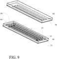
- FIG. 9 The partially assembled view shown in FIG. 9 demonstrates the tape layer 14 received in the well 60 with the metal layer 70 extending to the full lateral length and width dimensions of the capping substrate 68 and the metal layer 72 covering the outer surface of the lower substrate 60.
- FIG. 10 shows the flow cell 80 as completely assembled and laser bonded.
- the metal layer 70 may be etched to provide electrical contacts as previously described with respect to FIGs. 3 and 4 .
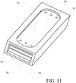
- FIG. 11 shows a chip enclosure 82 having a rectangular cavity 84 with an opening 86 in one side 88 receives the flow cell 20.
- An aperture 90 in one or both of the top and bottom of the chip enclosure 82 allows viewing of the flow channels.
- the cavity 84 has a height 92 corresponding to the thickness of the assembled flow cell 20. The height may be designed to require slight compression of the How cell for insertion into the cavity to enhance the sealing of the flow channels 15 by compressing the substrates 10, 16 (with the metal layers 12, 18) firmly against the tape layer 14.
- the chip enclosure 82 enclosure can be a single monolithic piece (machined or molded) or two halves permanently bonded/bolted together), and it can be reusable. It can be of any material, preferably a polymer or metal (for example Delrin, polyurethane, aluminum or stainless steel).
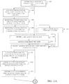
- a substrate is provided with a deposited metal layer on one surface, step 1302.
- the metal layer may be etched or otherwise formed to include mating cutouts for viewing flow channels, step 1304.
- the layer may additionally be etched or otherwise formed to include integral electrical leads, step 1306, and, in certain cases, conductive traces, step 1308,
- a tape layer is adhered to the substrate, step 1310.
- the tape layer is then laser cut to form flow channels, step 1312.
- dicing lines may additionally be cut for separation of flow cells on the wafer, step 1314.
- a mating substrate is provided with a second deposited metal layer on one surface, step 1316.
- the second metal layer may be etched or otherwise formed to include mating cutouts for viewing the flow channels, step 1318.
- the second metal layer may additionally be etched or otherwise formed to include integral electrical leads, step 1320, and, in certain cases, conductive traces, step 1322.
- the mating substrate is then aligned with and bonded to the tape layer, step 1324.
- the substrate, tape layer and mating substrate may be fully assembled without having the cutouts previously structured and an etchant introduced into the flow channels created by the tape layer to etch the mating cutouts in the first and second metal layer, step 1325. If processed as a wafer, the individual flow cells are then diced, step 1326.
- dicing of the first wafer may occur after laser cutting of the tape flow channels and dicing lines and individual mating substrates may then be applied to the individual cell masks.
- the substrates mating at the edges surrounding the well are engaged, step 1328, and room temperature laser bonding is accomplished to seal the flow cell, step 1330.
- an optional chip enclosure may be fabricated by introducing a rectangular cavity with an opening at one end in a case, step 1332. Apertures for viewing of the flow channels may be introduced into the chip enclosure, step 1334. The flow cell is then inserted, potentially with slight compression, into the cavity, step 1336.
Landscapes
- Chemical & Material Sciences (AREA)
- Engineering & Computer Science (AREA)
- Ceramic Engineering (AREA)
- Health & Medical Sciences (AREA)
- Chemical Kinetics & Catalysis (AREA)
- Clinical Laboratory Science (AREA)
- Hematology (AREA)
- General Health & Medical Sciences (AREA)
- Analytical Chemistry (AREA)
- Dispersion Chemistry (AREA)
- General Chemical & Material Sciences (AREA)
- Organic Chemistry (AREA)
- Metallurgy (AREA)
- Mechanical Engineering (AREA)
- Materials Engineering (AREA)
- Micromachines (AREA)
- Laser Beam Processing (AREA)
- Physical Or Chemical Processes And Apparatus (AREA)
Description
- Embodiments of the disclosure relate generally to the field of taped interlayer flow cells and more particularly to a method and structure for producing a taped interlayer flow cell with precision tape geometry and cell assembly including masking of the tape layer and conductive trace formation. The invention is defined in claim 1.
- Microfluidic devices, often referred to as flow cells, provide very precise means to carry out complicated biochemical reactions to acquire important chemical and biological information. Among other advantages, microfluidic systems reduce the required number of samples and quantities of reagents employed, shorten the response time of reactions, and decrease the amount of biohazard waste for disposal. First developed in the 1990s, initial microfluidic devices were fabricated in silicon and glass using photolithography and etching techniques adapted from the microelectronics industry. Many current microfluidic devices made using this method of fabrication are constructed from plastic, silicone or other polymeric materials, e.g. polydimethylsiloxane (PDMS). Such devices are generally expensive, inflexible, and difficult to construct. Examples of layered microfluidic devices are known from
US 2012/052250 A1 ,US 2005/023765 A1 ,US 2004/154923 A1 ,WO 2009/102688 A2 andWO 01/25138 A1 - Use of a tape interlayer to form the necessary microfluidic channels between two substrates was developed to reduce cost and complexity of fabrication. Typically a double-sided tape is used between two transparent substrates, which consists of a carrier material with an adhesive layer on the top and bottom and a removable liner covering the adhesive layers. Preferred double-sided tapes for all the embodiments described herein include double-sided silicone tape 3M 96042 or double-sided acrylic/silicone tape 3M 9731, but the choice of tape is dependent on the materials being used.
- Microchannels are created by cutting out parts of the double-sided tape and covering it with a sheet of material--glass is preferable for the base, plastics can alternatively be used as the top or bottom cover. Microchannels can be created in plastics or other materials by embossing, etching, or any structuring method. Any number of microfluidic device components can be included on the tape. These might include, for example, microchannels, microvalves or other pneumatic elements, diffusion chambers, manifolds, holes that connect one layer to another (vias), inlet and outlet ports, and other microfluidic device components.
- Conventional flow cell fabrication via molding, etching, and bonding is more expensive (both in required tooling and processing) and has longer lead time. In many cases, bonding methods to enclose the flow cell require high temperatures which prevent the use of many surface coatings and the encapsulation of fluids or live cultures.
- For prior art involving tape, no prior art fabrication methods provide capability for high precision formation of the flow channels. Additionally, imperfections in the tape as adhered to the substrates is aesthetically displeasing. In applications where the tape bonding to the substrates does not provide sufficient sealing no prior art technique is available to economically provide such sealing. Further, in many cases where electrical contact with the flow channels is needed, external leads must be employed. Finally, the prior art fabrication methods with tape cannot be accomplished on wafer level processing due to issues dicing the components on a wafer containing a tape layer.
- It is therefore desirable to provide an apparatus and method to obtain high precision in flow channel shaping, provide visual masking to hide imperfections in the tape, provide additional room temperature bonding of substrate edges to obtain better channel dimensional properties or a fast customization of the flow cell. Additionally it is desirable to provide integral electrical leads to the flow cell. Further it is desirable to provide on wafer level processing for dicing the components on a wafer containing a tape layer.
- According to the invention, disclosed is a flow cell having a first substrate with a metal layer on one surface. A tape layer having flow channels is adhered to the first substrate. A second substrate having a second metal layer on one surface is adhered to the tape layer opposite the first substrate. The first and second metal layers include mating cutouts to allow viewing of the flow channels.
- The embodiments disclosed provide a method for fabrication of a flow cell wherein a substrate is provided with a deposited metal layer on one surface. A tape layer is adhered to the substrate. The metal layer is etched prior to or after taping or otherwise formed to include mating openings for viewing flow channels. A mating substrate is provided with a second deposited metal layer on one surface. The mating substrate may contain holes that connect to the flow channels. The second metal layer may be etched or otherwise formed to include mating openings for viewing the flow channels. The mating substrate is then aligned with and bonded to the tape layer.
- The features, functions, and advantages that have been discussed can be achieved independently in various embodiments of the present disclosure or may be combined in yet other embodiments further details of which can be seen with reference to the following description and drawings.
-
-
FIG. 1 is an exploded perspective representation of one embodiment; -
FIG. 2 is a perspective representation of the embodiment ofFIG. 1 as assembled; -
FIG. 3 is an exploded perspective representation of a second embodiment incorporating integral conductive elements; -
FIG. 4 is a perspective representation of the embodiment ofFIG. 3 as assembled; -
FIG. 5 is a perspective representation of a wafer with tape elements having laser cut features; -
FIG. 6 is a perspective representation of the wafer ofFIG. 5 with the tape elements separated by laser cut part lines for dicing; -
FIG. 7 is a perspective view of an exemplary laser cutting station; -
FIG. 8 is an exploded perspective representation of a third embodiment incorporating a well in one substrate which receives the tape layer; -
FIG 9 is a perspective representation of the embodiment ofFIG. 8 as partially assembled; -
FIG. 10 is a perspective representation of the embodiment ofFIG. 8 as fully assembled; -
FIG. 11 is a perspective view of a chip enclosure adapted to receive a flow cell embodiment as shown inFIG. 1 ; -
FIG 12 is a sectioned perspective view of the chip enclosure ofFIG. 11 ; -
FIGs. 13A and13B are a flow charts demonstrating a method of assembly of a flow cell for the embodiments described. - Embodiments disclosed herein provide methods and apparatus for fabricating a taped interlayer flow cell. None of the prior art use a laser to obtain high precision, have a metallization layer to hide the imperfections in the tape, use a removable tape (UV release), or combine a standard well with a room temperature bonded edges to obtain better channel dimensional properties or a fast customization of the flow cell. Use of UV or thermally releasable tape also allows the flow cell to be easily disassembled, which may be advantageous for certain applications. Also, adding electrical leads to the flow cell is a challenge and normally accomplished with external leads. Finally, the prior art fabrication methods with tape cannot be done on wafer level processing due to issues dicing the components on a wafer containing a tape layer.
- Referring to the drawings,
FIG. 1 shows a first embodiment of a flow cell having a first ortop substrate 10 with one or more inlet/exit holes 11. Ametal layer 12 is deposited on an upper or lower surface of the first substrate (a lower surface deposition being shown inFIG. 1 ). Atape layer 14 with one or more lasercut flow channels 15 has double sided adhesive to adhere to themetal layer 12 on first and second substrate (to be described subsequently). Themetal layer 12 hasmating cutouts 13 sized to expose theflow channels 15. With the tape layer adhered to the metal layer or, in embodiments with the metal layer on an upper surface of the first substrate, the first substrate, an enclosed flow cell running between the inlet/exit ports 11 is created. Thetape layer 14 may have a temporary cover layer that can be removed to expose the adhesive as necessary. Thesubstrate 10 is transparent to allow viewing of the flow channel through thecutouts 13 in themetal layer 12 and may be also be predominantly transparent to a predetermined wavelength of a laser employed for processing as will be described subsequently, which will prevent excessive heat being generated at the interface. - A second or
bottom substrate 16 has asecond metal layer 18 deposited on an upper or lower surface (an upper surface deposition being shown inFIG. 1 ). The second metal layer incorporatescutouts 19 sized to expose theflow channels 15 and thesubstrate 16 is also transparent to allow viewing of theflow channels 15. The double sided adhesive on thetape layer 14 adheres to either themetal layer 18 or thesubstrate 16 depending on the surface on which the metal layer is deposited. For exemplary embodiments, thefirst substrate 10 andsecond substrate 16 may be glass, silicon, ceramic, plastic, or similar transparent materials. The metal layers 12, 18 are typically chromium for glass substrates but may employ alternative metals. Thetape layer 14 is a flexible PVC with synthetic acrylic adhesive bonded to both sides, similar to semiconductor wafer dicing tape supplied by companies like Lintec or Semiconductor Equipment Corporation. The tape layer may alternatively be masking tapes made of Kapton polyimide or polyester or have a silicon adhesive - In the assembled condition as shown in
FIG. 2 , theflow cell 20 allows viewing of the flow channels through the cutouts in the first and second metal layers. The tape layer with double sided adhesive bonds with both substrates. The metal layers on the substrates cover the adhesive attachment of the tape layer to the substrates thereby providing aesthetic masking of any imperfections in the adhesive such as bubbles, striations or graininess that would be visible through the transparent substrates. Thecutouts flow channels 15 in the tape layer or may be undersized to mask a portion of the flow cell. The cutouts may be formed in the metal layers on the substrates prior to assembly of the substrates, or they may be formed after assembly by running an etchant through the completed flow cell channels. Using undersized cut outs or forming the cutouts after assembly eliminates the need for exact alignment of the cut outs to the flow channels. Lateral masking across the flow channels may be employed for process marking or other visual functions associated with the flow cell. - The metal layers may additionally provide integral electrical conductors for process functions associated with the flow channels as shown in
FIGs. 3 and4 . The metal layers 12, 18 may be deposited on the substrates and structured by etching or laser processing to provide thecutouts flow channels 15. For the embodiment shown, the leads are present in thesecond metal layer 18 deposited on thesecond substrate 16. As shown inFIG. 3 , theleads 22 may be attached to contactpads 23 for external electrical connection. While two simple leads for one channel are shown inFIG. 3 , multiple leads extending from multiple sides of the flow cell may be provided and conductors etched within the metal layers for isolated interconnection between or around flow channels.Cutouts 24 are provided in thetape layer 14,upper metal layer 12 andtop substrate 10 to expose thecontact pads 23 for electrical connection with external circuitry. Thetape layer 14 provides insulation between thefirst metal layer 12 andsecond metal layer 18 for embodiments in which the metal layers are on interior surfaces of the substrates. - Processing of the tape layer for creation of the flow channels may be accomplished employing a
wafer 25 of the substrate material, which may contain a plurality of individual chips that are later diced into separate units as shown inFIG. 5 . For the embodiment shown a round wafer is employed and tape adhered to the wafer is initially cut leaving a pattern of multiple tape layers 14.FIG. 5 is shown with the excess tape removed. Thewafer 25 is put in afixture 28 mounted to the x axis and y axis motion stage on a laser bonding machine as disclosed in copending application serial no.13/291,956 FIG. 7 , Thefixture 28 can use a vacuum chuck or any comparable means to clamp the substrate work piece. Apositioning system 30 incorporates anx-axis motion stage 32 mounted on abase 33 and a y-axis motion stage 34 mounted to the x-axis mounting stage. For the embodiment shown, asubstrate alignment fixture 28 is mounted on the y-axis motion stage. However, in alternative embodiments, the motion stages may be reversed in vertical stacking and the alignment fixture mounted on the x-axis stage. Each motion stage has adrive motor 38 with associatedscrew drive 40 or similar translation mechanism.Covers 42 shield the operating elements of the motion stages for operator safety. A gantry 44 provides support foralignment optics 46 for thelaser 14, and for a z-motion stage, that carries final focusingoptics 48,camera 50 and other instrumentation systems as required for monitoring and controling the bonding operation. For the embodiment shown, apower meter 52 is mounted to the x-axis motion stage to be positioned under the laser optical train for measurement and/or calibration of laser power before movement of the alignment fixture under the laser optics for tape cutting. In the embodiment shown, a z-axis motion stage 54 is provided for vertical positioning of the optical and measurement systems with respect to the alignment fixture. Acomputer controller 55 is programmable for translation of the x-axis, y-axis and z-axis motion stages for translation of the laser on the work piece. A single laser may be employed for illuminating multiple substrate work pieces in individual positioning systems by employing beam splitters and focusing optical trains to the multiple positioning systems. It is also possible to replace the fixed lens with an f-theta lens with an X-Y scanner and Z-auto-focus either by itself or in conjunction with a large travel X-Y positioning system. - The laser is focused on the tape layer, and the stage is traversed to cut
precise flow channels 15. The laser may ablate the tape creating the flow channels or the laser may cut an outline of the channels and then the inner portion of the outline is subsequently removed from the substrate. For embodiments as disclosed previously and described with respect toFIGs. 1-4 , a second substrate wafer is then aligned with the first and bonded to the taped side of the first substrate wafer, thereby enclosing or capping the flow cells. Either prior to or after these processing steps, one or both substrates may have through holes (manufactured by any means) located at precise locations to create inlets and exits of the flow cell. - The embodiments disclosed allow dicing the tape inner layer flow cells from a wafer containing multiple chips. The typical method is using a dicing saw. However, in the case of a flow cell constructed with a tape inner layer, the tape can create a seal with the cutting blade which restricts cooling fluid from flowing into the kerf and causes the blade to overheat. In the proposed method, the tape can be removed from the dicing
lines 26 as shown inFIG. 6 to create individual tape layer masks prior to the dicing operation via laser ablation or laser cutting in a similar fashion used to create theflow channels 15 and at the same time. This leaves a clear path for the dicing saw and cooling fluid. In an alternative embodiment, the dicing lines may have sufficient width to space the tape layer masks for placement in a well in a substrate as will be described subsequently. An additional processing step would be to the pre-dice the wafer prior to application of the tape, and leave small areas (tabs) to hold the wafer together as a monolithic unit. After application of the tape layer and processing as described to create theflow channels 15 and dicinglines 26, only the small tab areas will need to be cut to separate the individual chips. The small tab areas can be cut with the laser either during or after the tape cutting process thereby eliminating the saw cutting of the completed wafer. - As shown in
FIG. 8 , in another embodiment of the taped flow cell, thetape layer 14 is received inside a well 60 in abottom substrate 62. The well is designed such that theheight 63 of the well 60 is a precise dimension that defines the desired height of the flow cell. The well height would preferably be slightly less than the thickness of thetape layer 14, such that it provides some compressive force on the tape to improve adhesion and pressure capacity of the flow cell upon assembly as described subsequently. Theoutside edges 64 of thebottom substrate 62 surrounding the well 60 would also provide aflat surface 66 which can be laser bonded to the cappingsubstrate 68 which haslength 69a andwidth 69b sufficient to overlap theedges 64 in thelower substrate 62. Theflat surface 66 on theedges 64 insures that the top and bottom surfaces of theflow channels 15 are parallel to each other within a significantly tighter tolerance than a flow cell fabricated with tape alone as the inner layer. The cappingsubstrate 68 has ametal layer 70 on an inner surface to engage thetape layer 14 and theedges 64 of thebottom substrate 62. A room temperature laser bond may then be established at the interface of the mated lower and capping substrates, employing themetal layer 70 to create the localized plasma as described in application serial no.13/291,956 metal layer 70 extending over theflat surface 66 on theedges 64 provides a boundary region surrounding the well 60 for creation of the localized plasma. For the embodiment ofFIG. 8 , asecond metal layer 72 may be deposited on the outer flat surface of thelower substrate 62. As previously described with respect to the prior embodiments,mating cutouts respective metal layers flow channels 15 created in thetape layer 14. - The partially assembled view shown in
FIG. 9 demonstrates thetape layer 14 received in the well 60 with themetal layer 70 extending to the full lateral length and width dimensions of the cappingsubstrate 68 and themetal layer 72 covering the outer surface of thelower substrate 60.FIG. 10 shows theflow cell 80 as completely assembled and laser bonded. Themetal layer 70 may be etched to provide electrical contacts as previously described with respect toFIGs. 3 and4 . - For embodiments as disclosed and described with respect to
FIGs, 1 ,2 ,3 and4 , additional support for the flow cell beyond the strength of the adhesive bond between the tape layer and substrates may be desirable.Fig. 11 shows achip enclosure 82 having arectangular cavity 84 with anopening 86 in oneside 88 receives theflow cell 20. Anaperture 90 in one or both of the top and bottom of thechip enclosure 82 allows viewing of the flow channels. As shown inFIG. 12 , thecavity 84 has aheight 92 corresponding to the thickness of the assembledflow cell 20. The height may be designed to require slight compression of the How cell for insertion into the cavity to enhance the sealing of theflow channels 15 by compressing thesubstrates 10, 16 (with the metal layers 12, 18) firmly against thetape layer 14. Thechip enclosure 82 enclosure can be a single monolithic piece (machined or molded) or two halves permanently bonded/bolted together), and it can be reusable. It can be of any material, preferably a polymer or metal (for example Delrin, polyurethane, aluminum or stainless steel). - The embodiments described provide a method for fabricating a flow cell as shown in
FIGs. 13A and13B . A substrate is provided with a deposited metal layer on one surface,step 1302. The metal layer may be etched or otherwise formed to include mating cutouts for viewing flow channels,step 1304. The layer may additionally be etched or otherwise formed to include integral electrical leads,step 1306, and, in certain cases, conductive traces,step 1308, A tape layer is adhered to the substrate,step 1310. The tape layer is then laser cut to form flow channels, step 1312. In a wafer processing approach, dicing lines may additionally be cut for separation of flow cells on the wafer,step 1314. A mating substrate is provided with a second deposited metal layer on one surface,step 1316. The second metal layer may be etched or otherwise formed to include mating cutouts for viewing the flow channels,step 1318. The second metal layer may additionally be etched or otherwise formed to include integral electrical leads,step 1320, and, in certain cases, conductive traces,step 1322. The mating substrate is then aligned with and bonded to the tape layer,step 1324. In an alternative sequencing, the substrate, tape layer and mating substrate may be fully assembled without having the cutouts previously structured and an etchant introduced into the flow channels created by the tape layer to etch the mating cutouts in the first and second metal layer,step 1325. If processed as a wafer, the individual flow cells are then diced,step 1326. Alternatively, dicing of the first wafer may occur after laser cutting of the tape flow channels and dicing lines and individual mating substrates may then be applied to the individual cell masks. For embodiments employing a substrate with a well receiving the tape layer, the substrates mating at the edges surrounding the well are engaged,step 1328, and room temperature laser bonding is accomplished to seal the flow cell,step 1330. If a flow cell as described with respect toFIGs. 1 and2 is employed, an optional chip enclosure may be fabricated by introducing a rectangular cavity with an opening at one end in a case,step 1332. Apertures for viewing of the flow channels may be introduced into the chip enclosure,step 1334. The flow cell is then inserted, potentially with slight compression, into the cavity,step 1336. - Having now described various embodiments of the disclosure in detail as required by the patent statutes, those skilled in the art will recognize modifications and substitutions to the specific embodiments disclosed herein. Such modifications are within the scope of the present disclosure as defined in the following claims.
Claims (9)
- A taped interlayer flow cell comprising:a first substrate (10);a second substrate (16); anda double-sided tape (14) disposed between the first substrate (10) and the second substrate (16) and comprising a carrier material, adhesive layers on top and bottom surfaces of the carrier material, and a flow channel formed (15) therein;wherein the first substrate (10) comprises a first transparent substrate and a first masking layer (12) depositedon the transparent substrate to cover adhesive attachment of the double-sided tape (14) to the first substrate (10);wherein the masking layer (12) comprises a mating cutout (13) to at least partially expose the flow channel of the double-sided tape (14);wherein the second substrate (16) comprises a second transparent substrate and a second masking layer (18) depositedon the second transparent substrate to cover adhesive attachment of the double-sided tape (14) to the second substrate (16); andwherein the first masking layer (12) and the second masking layer (18) are metal layers and each have a matingcutout (13, 19) that are aligned to allow viewing of the same flow channel (15) through both the first substrate (10) and the second substrate (16).
- The taped interlayer flow cell of claim 1, wherein:the adhesive layer on the top surface of the carrier material and adhered to the first substrate (10) is masked by the first masking layer (12); andthe flow channel (15) of the double-sided tape (14) is visible through the mating cutout (13) in the first masking layer (12).
- The taped interlayer flow cell of claim 1 or claim 2, wherein the second substrate (16) comprises a silicon substrate.
- The taped interlayer flow cell of claim 1 or claim 2, wherein:The first masking layer (12) is disposed on a bottom surface of the transparent substrate and adjacent the double-sided tape (14); andthe second masking layer (18) is disposed on a top surface of the second transparent substrate and adjacent the double-sided tape (14).
- The taped interlayer flow cell of claim 4, wherein each of the first masking layer (12) and the second masking layer (18) is an electrical conductor, and the double-sided tape is an insulation between the first masking layer (12) and the second masking layer (18).
- The taped interlayer flow cell of claim 4 or claim 5, wherein at least one of the mating cutout (13) in the first masking layer (12) or the mating cutout (19) in the second masking layer (18) is sized and shaped identically to the flow channel (15) of the double-sided tape (14).
- The taped interlayer flow cell of claim 4 or claim 5, wherein at least one of the mating cutout (13) in the first masking layer (12) or the mating cutout (19) in the second masking layer (18) is undersized to mask a portion of the flow channel (15) of the double-sided tape (14).
- The taped interlayer flow cell of any of claims 4 to 7, wherein at least one of the first masking layer (12) or the second masking layer (18) comprises a lateral masking across the flow channel (15) of the double-sided tape (14).
- The taped interlayer flow cell of any of claims 1 to 8, wherein at least one of:(a) the adhesive layers of the double-sided tape (14) comprise an acrylic adhesive or a silicone adhesive; or
the carrier material of the double-sided tape (14) comprises polyvinyl chloride (PVC), polyimide, or polyester.
Applications Claiming Priority (2)
| Application Number | Priority Date | Filing Date | Title |
|---|---|---|---|
| US14/498,003 US9795963B2 (en) | 2014-09-26 | 2014-09-26 | Method and apparatus for taped interlayer flow cell with masking and conductive traces |
| PCT/US2014/068964 WO2016048398A1 (en) | 2014-09-26 | 2014-12-06 | Method and apparatus for taped interlayer flow cell with masking and conductive traces |
Publications (3)
| Publication Number | Publication Date |
|---|---|
| EP3197601A1 EP3197601A1 (en) | 2017-08-02 |
| EP3197601A4 EP3197601A4 (en) | 2018-07-25 |
| EP3197601B1 true EP3197601B1 (en) | 2020-08-26 |
Family
ID=55581707
Family Applications (1)
| Application Number | Title | Priority Date | Filing Date |
|---|---|---|---|
| EP14902533.0A Active EP3197601B1 (en) | 2014-09-26 | 2014-12-06 | Taped interlayer flow-cell with metallic masking layers |
Country Status (5)
| Country | Link |
|---|---|
| US (2) | US9795963B2 (en) |
| EP (1) | EP3197601B1 (en) |
| JP (1) | JP6552611B2 (en) |
| CN (1) | CN107847928A (en) |
| WO (1) | WO2016048398A1 (en) |
Families Citing this family (5)
| Publication number | Priority date | Publication date | Assignee | Title |
|---|---|---|---|---|
| US10285640B2 (en) * | 2015-10-21 | 2019-05-14 | Simon Fraser University | Process and method for fabricating wearable and flexible microfluidic devices and systems |
| CN107715932B (en) * | 2017-11-23 | 2023-06-16 | 昌微系统科技(上海)有限公司 | Microfluidic device |
| KR102122415B1 (en) * | 2018-08-13 | 2020-06-12 | 한국과학기술원 | Microfluidic device for gene collection and gene collection method using the same |
| CN113457758B (en) * | 2021-07-14 | 2023-05-23 | 浙江理工大学 | Micro-fluidic channel for admittance type sweat rate measurement |
| JP7527529B2 (en) | 2022-06-30 | 2024-08-02 | Nok株式会社 | Microfluidic Devices |
Family Cites Families (26)
| Publication number | Priority date | Publication date | Assignee | Title |
|---|---|---|---|---|
| JPS5074932A (en) | 1973-11-02 | 1975-06-19 | ||
| JPS5852846A (en) * | 1981-09-25 | 1983-03-29 | Oki Electric Ind Co Ltd | Manufacture of semiconductor device |
| JPH0574932A (en) * | 1991-09-17 | 1993-03-26 | Fujitsu Ltd | Dicing method for semiconductor wafer |
| US6425972B1 (en) * | 1997-06-18 | 2002-07-30 | Calipher Technologies Corp. | Methods of manufacturing microfabricated substrates |
| US6830934B1 (en) * | 1999-06-15 | 2004-12-14 | Lifescan, Inc. | Microdroplet dispensing for a medical diagnostic device |
| EP1222141A1 (en) * | 1999-10-04 | 2002-07-17 | Nanostream, Inc. | Modular microfluidic devices comprising sandwiched stencils |
| US6672502B1 (en) | 2000-11-28 | 2004-01-06 | The State Of Oregon Acting By And Through The State Board Of Higher Education On Behalf Of Oregon State University | Method for making devices having intermetallic structures and intermetallic devices made thereby |
| US20050023765A1 (en) * | 2002-01-31 | 2005-02-03 | Coombs James Howard | Bio-safety features for optical analysis disc and disc system including same |
| DE10234819A1 (en) * | 2002-07-31 | 2004-02-19 | Roche Diagnostics Gmbh | Test apparatus for blood, comprising compound body with test strip levels and transport channels to give complex tests in compact structure |
| US20050003521A1 (en) * | 2003-03-11 | 2005-01-06 | O'connor David | Addressable microarray device, methods of making, and uses thereof |
| JP2006030160A (en) * | 2004-04-14 | 2006-02-02 | Hitachi Maxell Ltd | Reaction container |
| US20050272142A1 (en) * | 2004-04-14 | 2005-12-08 | Hitachi Maxwell, Ltd. | Fluid vessel |
| CN101356441B (en) * | 2005-10-25 | 2011-06-15 | 株式会社岛津制作所 | Flow through cell and manufacturing method thereof |
| GB0620955D0 (en) * | 2006-10-20 | 2006-11-29 | Speakman Stuart P | Methods and apparatus for the manufacture of microstructures |
| US20090074615A1 (en) * | 2007-09-17 | 2009-03-19 | Ysi Incorporated | Microfluidic module including an adhesiveless self-bonding rebondable polyimide |
| WO2009096527A1 (en) * | 2008-02-01 | 2009-08-06 | Nippon Telegraph And Telephone Corporation | Flow cell |
| US8173080B2 (en) * | 2008-02-14 | 2012-05-08 | Illumina, Inc. | Flow cells and manifolds having an electroosmotic pump |
| DE102010002921A1 (en) * | 2010-03-16 | 2011-09-22 | Senslab-Gesellschaft Zur Entwicklung Und Herstellung Bioelektrochemischer Sensoren Mbh | Microfluidic multiple measuring chamber arrangement |
| US20120052250A1 (en) * | 2010-08-27 | 2012-03-01 | Derosa Michael Edward | Flexible Microfluidic Device with Interconnected Porous Network |
| US20140179909A1 (en) * | 2010-11-30 | 2014-06-26 | Quantumdx Group Limited | Microfluidic device for nucleic acid extraction and fractionation |
| JP5852846B2 (en) | 2010-12-28 | 2016-02-03 | アスモ株式会社 | motor |
| US8912077B2 (en) * | 2011-06-15 | 2014-12-16 | Applied Materials, Inc. | Hybrid laser and plasma etch wafer dicing using substrate carrier |
| US8975193B2 (en) * | 2011-08-02 | 2015-03-10 | Teledyne Dalsa Semiconductor, Inc. | Method of making a microfluidic device |
| US9492990B2 (en) * | 2011-11-08 | 2016-11-15 | Picosys Incorporated | Room temperature glass-to-glass, glass-to-plastic and glass-to-ceramic/semiconductor bonding |
| US10537889B2 (en) | 2013-12-31 | 2020-01-21 | Illumina, Inc. | Addressable flow cell using patterned electrodes |
| JP2017518752A (en) * | 2014-06-12 | 2017-07-13 | ウエハージェン インコーポレイテッド | Single cell capture using a capture polymer membrane |
-
2014
- 2014-09-26 US US14/498,003 patent/US9795963B2/en not_active Expired - Fee Related
- 2014-12-06 EP EP14902533.0A patent/EP3197601B1/en active Active
- 2014-12-06 JP JP2017516938A patent/JP6552611B2/en not_active Expired - Fee Related
- 2014-12-06 CN CN201480083656.2A patent/CN107847928A/en active Pending
- 2014-12-06 WO PCT/US2014/068964 patent/WO2016048398A1/en active Application Filing
-
2017
- 2017-09-07 US US15/697,771 patent/US10512909B2/en active Active
Non-Patent Citations (1)
| Title |
|---|
| None * |
Also Published As
| Publication number | Publication date |
|---|---|
| EP3197601A1 (en) | 2017-08-02 |
| US9795963B2 (en) | 2017-10-24 |
| WO2016048398A1 (en) | 2016-03-31 |
| CN107847928A (en) | 2018-03-27 |
| US20160089671A1 (en) | 2016-03-31 |
| JP6552611B2 (en) | 2019-07-31 |
| JP2017537797A (en) | 2017-12-21 |
| EP3197601A4 (en) | 2018-07-25 |
| US20170361320A1 (en) | 2017-12-21 |
| US10512909B2 (en) | 2019-12-24 |
Similar Documents
| Publication | Publication Date | Title |
|---|---|---|
| US10512909B2 (en) | Method and apparatus for taped interlayer flow cell with masking | |
| RU2422204C2 (en) | Encased carrier system for electronic micro fluid devices | |
| US11198119B2 (en) | Fabrication of a microfluidic chip package or assembly with separable chips | |
| US6821819B1 (en) | Method of packaging and assembling micro-fluidic device | |
| EP1950569A1 (en) | Flow cell and process for producing the same | |
| EP1960488B1 (en) | Fine line sealing and channel lining system and method | |
| WO2003070623A1 (en) | Micro fluid system support unit and manufacturing method thereof | |
| US8911636B2 (en) | Micro-device on glass | |
| US7965516B2 (en) | Power semiconductor module and method for its production | |
| JP4488704B2 (en) | Microfluidic device and microfluidic device integration method | |
| EP1926356A1 (en) | Product having a solid body and one or more rooms inside | |
| EP2390225A2 (en) | Method of dividing a substrate into a plurality of individual chip parts | |
| JP4963437B2 (en) | Flow path body, wiring board, flow path forming wiring board, flow path forming method, flow path body manufacturing method, and flow path body kit | |
| Gaikwad | Microchannel heat sink fabrication technique | |
| CN111668175A (en) | Board-level fan-out type heat dissipation structure, preparation method thereof and electronic component | |
| Thompson | Reversible concentric ring microfluidic interconnects |
Legal Events
| Date | Code | Title | Description |
|---|---|---|---|
| STAA | Information on the status of an ep patent application or granted ep patent |
Free format text: STATUS: THE INTERNATIONAL PUBLICATION HAS BEEN MADE |
|
| PUAI | Public reference made under article 153(3) epc to a published international application that has entered the european phase |
Free format text: ORIGINAL CODE: 0009012 |
|
| STAA | Information on the status of an ep patent application or granted ep patent |
Free format text: STATUS: REQUEST FOR EXAMINATION WAS MADE |
|
| 17P | Request for examination filed |
Effective date: 20170420 |
|
| AK | Designated contracting states |
Kind code of ref document: A1 Designated state(s): AL AT BE BG CH CY CZ DE DK EE ES FI FR GB GR HR HU IE IS IT LI LT LU LV MC MK MT NL NO PL PT RO RS SE SI SK SM TR |
|
| AX | Request for extension of the european patent |
Extension state: BA ME |
|
| DAX | Request for extension of the european patent (deleted) | ||
| RIC1 | Information provided on ipc code assigned before grant |
Ipc: B32B 27/28 20060101ALI20180301BHEP Ipc: B32B 27/36 20060101ALI20180301BHEP Ipc: B32B 27/30 20060101ALI20180301BHEP Ipc: B32B 15/18 20060101ALI20180301BHEP Ipc: B32B 9/04 20060101ALI20180301BHEP Ipc: B32B 15/20 20060101ALI20180301BHEP Ipc: B32B 7/06 20060101ALI20180301BHEP Ipc: B32B 27/06 20060101ALI20180301BHEP Ipc: B32B 3/04 20060101ALI20180301BHEP Ipc: B32B 9/00 20060101ALI20180301BHEP Ipc: B01L 3/00 20060101AFI20180301BHEP Ipc: B32B 3/26 20060101ALI20180301BHEP Ipc: B32B 27/08 20060101ALI20180301BHEP Ipc: B32B 27/40 20060101ALI20180301BHEP Ipc: B32B 15/08 20060101ALI20180301BHEP Ipc: B32B 7/12 20060101ALI20180301BHEP |
|
| A4 | Supplementary search report drawn up and despatched |
Effective date: 20180626 |
|
| RIC1 | Information provided on ipc code assigned before grant |
Ipc: B32B 15/08 20060101ALI20180620BHEP Ipc: B32B 27/30 20060101ALI20180620BHEP Ipc: B32B 7/06 20060101ALI20180620BHEP Ipc: B32B 27/08 20060101ALI20180620BHEP Ipc: B32B 7/12 20060101ALI20180620BHEP Ipc: B01L 3/00 20060101AFI20180620BHEP Ipc: B32B 27/28 20060101ALI20180620BHEP Ipc: B32B 3/04 20060101ALI20180620BHEP Ipc: B32B 27/36 20060101ALI20180620BHEP Ipc: B32B 15/20 20060101ALI20180620BHEP Ipc: B32B 15/18 20060101ALI20180620BHEP Ipc: B32B 9/00 20060101ALI20180620BHEP Ipc: B32B 9/04 20060101ALI20180620BHEP Ipc: B32B 27/40 20060101ALI20180620BHEP Ipc: B32B 27/06 20060101ALI20180620BHEP Ipc: B32B 3/26 20060101ALI20180620BHEP |
|
| RAP1 | Party data changed (applicant data changed or rights of an application transferred) |
Owner name: CORNING INCORPORATED |
|
| STAA | Information on the status of an ep patent application or granted ep patent |
Free format text: STATUS: EXAMINATION IS IN PROGRESS |
|
| 17Q | First examination report despatched |
Effective date: 20190712 |
|
| GRAP | Despatch of communication of intention to grant a patent |
Free format text: ORIGINAL CODE: EPIDOSNIGR1 |
|
| STAA | Information on the status of an ep patent application or granted ep patent |
Free format text: STATUS: GRANT OF PATENT IS INTENDED |
|
| INTG | Intention to grant announced |
Effective date: 20200304 |
|
| GRAJ | Information related to disapproval of communication of intention to grant by the applicant or resumption of examination proceedings by the epo deleted |
Free format text: ORIGINAL CODE: EPIDOSDIGR1 |
|
| STAA | Information on the status of an ep patent application or granted ep patent |
Free format text: STATUS: EXAMINATION IS IN PROGRESS |
|
| GRAR | Information related to intention to grant a patent recorded |
Free format text: ORIGINAL CODE: EPIDOSNIGR71 |
|
| GRAS | Grant fee paid |
Free format text: ORIGINAL CODE: EPIDOSNIGR3 |
|
| STAA | Information on the status of an ep patent application or granted ep patent |
Free format text: STATUS: GRANT OF PATENT IS INTENDED |
|
| GRAA | (expected) grant |
Free format text: ORIGINAL CODE: 0009210 |
|
| STAA | Information on the status of an ep patent application or granted ep patent |
Free format text: STATUS: THE PATENT HAS BEEN GRANTED |
|
| INTC | Intention to grant announced (deleted) | ||
| AK | Designated contracting states |
Kind code of ref document: B1 Designated state(s): AL AT BE BG CH CY CZ DE DK EE ES FI FR GB GR HR HU IE IS IT LI LT LU LV MC MK MT NL NO PL PT RO RS SE SI SK SM TR |
|
| INTG | Intention to grant announced |
Effective date: 20200722 |
|
| REG | Reference to a national code |
Ref country code: GB Ref legal event code: FG4D |
|
| REG | Reference to a national code |
Ref country code: CH Ref legal event code: EP |
|
| REG | Reference to a national code |
Ref country code: AT Ref legal event code: REF Ref document number: 1305852 Country of ref document: AT Kind code of ref document: T Effective date: 20200915 |
|
| REG | Reference to a national code |
Ref country code: IE Ref legal event code: FG4D |
|
| REG | Reference to a national code |
Ref country code: DE Ref legal event code: R096 Ref document number: 602014069557 Country of ref document: DE |
|
| REG | Reference to a national code |
Ref country code: LT Ref legal event code: MG4D |
|
| PG25 | Lapsed in a contracting state [announced via postgrant information from national office to epo] |
Ref country code: LT Free format text: LAPSE BECAUSE OF FAILURE TO SUBMIT A TRANSLATION OF THE DESCRIPTION OR TO PAY THE FEE WITHIN THE PRESCRIBED TIME-LIMIT Effective date: 20200826 Ref country code: BG Free format text: LAPSE BECAUSE OF FAILURE TO SUBMIT A TRANSLATION OF THE DESCRIPTION OR TO PAY THE FEE WITHIN THE PRESCRIBED TIME-LIMIT Effective date: 20201126 Ref country code: NO Free format text: LAPSE BECAUSE OF FAILURE TO SUBMIT A TRANSLATION OF THE DESCRIPTION OR TO PAY THE FEE WITHIN THE PRESCRIBED TIME-LIMIT Effective date: 20201126 Ref country code: GR Free format text: LAPSE BECAUSE OF FAILURE TO SUBMIT A TRANSLATION OF THE DESCRIPTION OR TO PAY THE FEE WITHIN THE PRESCRIBED TIME-LIMIT Effective date: 20201127 Ref country code: PT Free format text: LAPSE BECAUSE OF FAILURE TO SUBMIT A TRANSLATION OF THE DESCRIPTION OR TO PAY THE FEE WITHIN THE PRESCRIBED TIME-LIMIT Effective date: 20201228 Ref country code: FI Free format text: LAPSE BECAUSE OF FAILURE TO SUBMIT A TRANSLATION OF THE DESCRIPTION OR TO PAY THE FEE WITHIN THE PRESCRIBED TIME-LIMIT Effective date: 20200826 Ref country code: SE Free format text: LAPSE BECAUSE OF FAILURE TO SUBMIT A TRANSLATION OF THE DESCRIPTION OR TO PAY THE FEE WITHIN THE PRESCRIBED TIME-LIMIT Effective date: 20200826 Ref country code: HR Free format text: LAPSE BECAUSE OF FAILURE TO SUBMIT A TRANSLATION OF THE DESCRIPTION OR TO PAY THE FEE WITHIN THE PRESCRIBED TIME-LIMIT Effective date: 20200826 |
|
| REG | Reference to a national code |
Ref country code: NL Ref legal event code: MP Effective date: 20200826 |
|
| REG | Reference to a national code |
Ref country code: AT Ref legal event code: MK05 Ref document number: 1305852 Country of ref document: AT Kind code of ref document: T Effective date: 20200826 |
|
| PG25 | Lapsed in a contracting state [announced via postgrant information from national office to epo] |
Ref country code: IS Free format text: LAPSE BECAUSE OF FAILURE TO SUBMIT A TRANSLATION OF THE DESCRIPTION OR TO PAY THE FEE WITHIN THE PRESCRIBED TIME-LIMIT Effective date: 20201226 Ref country code: RS Free format text: LAPSE BECAUSE OF FAILURE TO SUBMIT A TRANSLATION OF THE DESCRIPTION OR TO PAY THE FEE WITHIN THE PRESCRIBED TIME-LIMIT Effective date: 20200826 Ref country code: LV Free format text: LAPSE BECAUSE OF FAILURE TO SUBMIT A TRANSLATION OF THE DESCRIPTION OR TO PAY THE FEE WITHIN THE PRESCRIBED TIME-LIMIT Effective date: 20200826 Ref country code: PL Free format text: LAPSE BECAUSE OF FAILURE TO SUBMIT A TRANSLATION OF THE DESCRIPTION OR TO PAY THE FEE WITHIN THE PRESCRIBED TIME-LIMIT Effective date: 20200826 Ref country code: NL Free format text: LAPSE BECAUSE OF FAILURE TO SUBMIT A TRANSLATION OF THE DESCRIPTION OR TO PAY THE FEE WITHIN THE PRESCRIBED TIME-LIMIT Effective date: 20200826 |
|
| PG25 | Lapsed in a contracting state [announced via postgrant information from national office to epo] |
Ref country code: DK Free format text: LAPSE BECAUSE OF FAILURE TO SUBMIT A TRANSLATION OF THE DESCRIPTION OR TO PAY THE FEE WITHIN THE PRESCRIBED TIME-LIMIT Effective date: 20200826 Ref country code: CZ Free format text: LAPSE BECAUSE OF FAILURE TO SUBMIT A TRANSLATION OF THE DESCRIPTION OR TO PAY THE FEE WITHIN THE PRESCRIBED TIME-LIMIT Effective date: 20200826 Ref country code: EE Free format text: LAPSE BECAUSE OF FAILURE TO SUBMIT A TRANSLATION OF THE DESCRIPTION OR TO PAY THE FEE WITHIN THE PRESCRIBED TIME-LIMIT Effective date: 20200826 Ref country code: RO Free format text: LAPSE BECAUSE OF FAILURE TO SUBMIT A TRANSLATION OF THE DESCRIPTION OR TO PAY THE FEE WITHIN THE PRESCRIBED TIME-LIMIT Effective date: 20200826 Ref country code: SM Free format text: LAPSE BECAUSE OF FAILURE TO SUBMIT A TRANSLATION OF THE DESCRIPTION OR TO PAY THE FEE WITHIN THE PRESCRIBED TIME-LIMIT Effective date: 20200826 |
|
| REG | Reference to a national code |
Ref country code: DE Ref legal event code: R097 Ref document number: 602014069557 Country of ref document: DE |
|
| PG25 | Lapsed in a contracting state [announced via postgrant information from national office to epo] |
Ref country code: ES Free format text: LAPSE BECAUSE OF FAILURE TO SUBMIT A TRANSLATION OF THE DESCRIPTION OR TO PAY THE FEE WITHIN THE PRESCRIBED TIME-LIMIT Effective date: 20200826 Ref country code: AT Free format text: LAPSE BECAUSE OF FAILURE TO SUBMIT A TRANSLATION OF THE DESCRIPTION OR TO PAY THE FEE WITHIN THE PRESCRIBED TIME-LIMIT Effective date: 20200826 Ref country code: AL Free format text: LAPSE BECAUSE OF FAILURE TO SUBMIT A TRANSLATION OF THE DESCRIPTION OR TO PAY THE FEE WITHIN THE PRESCRIBED TIME-LIMIT Effective date: 20200826 |
|
| PG25 | Lapsed in a contracting state [announced via postgrant information from national office to epo] |
Ref country code: SK Free format text: LAPSE BECAUSE OF FAILURE TO SUBMIT A TRANSLATION OF THE DESCRIPTION OR TO PAY THE FEE WITHIN THE PRESCRIBED TIME-LIMIT Effective date: 20200826 |
|
| REG | Reference to a national code |
Ref country code: DE Ref legal event code: R119 Ref document number: 602014069557 Country of ref document: DE |
|
| PLBE | No opposition filed within time limit |
Free format text: ORIGINAL CODE: 0009261 |
|
| STAA | Information on the status of an ep patent application or granted ep patent |
Free format text: STATUS: NO OPPOSITION FILED WITHIN TIME LIMIT |
|
| PG25 | Lapsed in a contracting state [announced via postgrant information from national office to epo] |
Ref country code: IT Free format text: LAPSE BECAUSE OF FAILURE TO SUBMIT A TRANSLATION OF THE DESCRIPTION OR TO PAY THE FEE WITHIN THE PRESCRIBED TIME-LIMIT Effective date: 20200826 |
|
| REG | Reference to a national code |
Ref country code: CH Ref legal event code: PL |
|
| 26N | No opposition filed |
Effective date: 20210527 |
|
| GBPC | Gb: european patent ceased through non-payment of renewal fee |
Effective date: 20201206 |
|
| PG25 | Lapsed in a contracting state [announced via postgrant information from national office to epo] |
Ref country code: SI Free format text: LAPSE BECAUSE OF FAILURE TO SUBMIT A TRANSLATION OF THE DESCRIPTION OR TO PAY THE FEE WITHIN THE PRESCRIBED TIME-LIMIT Effective date: 20200826 Ref country code: MC Free format text: LAPSE BECAUSE OF FAILURE TO SUBMIT A TRANSLATION OF THE DESCRIPTION OR TO PAY THE FEE WITHIN THE PRESCRIBED TIME-LIMIT Effective date: 20200826 |
|
| REG | Reference to a national code |
Ref country code: BE Ref legal event code: MM Effective date: 20201231 |
|
| PG25 | Lapsed in a contracting state [announced via postgrant information from national office to epo] |
Ref country code: FR Free format text: LAPSE BECAUSE OF NON-PAYMENT OF DUE FEES Effective date: 20201231 Ref country code: LU Free format text: LAPSE BECAUSE OF NON-PAYMENT OF DUE FEES Effective date: 20201206 Ref country code: IE Free format text: LAPSE BECAUSE OF NON-PAYMENT OF DUE FEES Effective date: 20201206 |
|
| PG25 | Lapsed in a contracting state [announced via postgrant information from national office to epo] |
Ref country code: GB Free format text: LAPSE BECAUSE OF NON-PAYMENT OF DUE FEES Effective date: 20201206 Ref country code: DE Free format text: LAPSE BECAUSE OF NON-PAYMENT OF DUE FEES Effective date: 20210701 Ref country code: CH Free format text: LAPSE BECAUSE OF NON-PAYMENT OF DUE FEES Effective date: 20201231 Ref country code: LI Free format text: LAPSE BECAUSE OF NON-PAYMENT OF DUE FEES Effective date: 20201231 |
|
| PG25 | Lapsed in a contracting state [announced via postgrant information from national office to epo] |
Ref country code: IS Free format text: LAPSE BECAUSE OF FAILURE TO SUBMIT A TRANSLATION OF THE DESCRIPTION OR TO PAY THE FEE WITHIN THE PRESCRIBED TIME-LIMIT Effective date: 20201226 Ref country code: TR Free format text: LAPSE BECAUSE OF FAILURE TO SUBMIT A TRANSLATION OF THE DESCRIPTION OR TO PAY THE FEE WITHIN THE PRESCRIBED TIME-LIMIT Effective date: 20200826 Ref country code: MT Free format text: LAPSE BECAUSE OF FAILURE TO SUBMIT A TRANSLATION OF THE DESCRIPTION OR TO PAY THE FEE WITHIN THE PRESCRIBED TIME-LIMIT Effective date: 20200826 Ref country code: CY Free format text: LAPSE BECAUSE OF FAILURE TO SUBMIT A TRANSLATION OF THE DESCRIPTION OR TO PAY THE FEE WITHIN THE PRESCRIBED TIME-LIMIT Effective date: 20200826 |
|
| PG25 | Lapsed in a contracting state [announced via postgrant information from national office to epo] |
Ref country code: MK Free format text: LAPSE BECAUSE OF FAILURE TO SUBMIT A TRANSLATION OF THE DESCRIPTION OR TO PAY THE FEE WITHIN THE PRESCRIBED TIME-LIMIT Effective date: 20200826 |
|
| PG25 | Lapsed in a contracting state [announced via postgrant information from national office to epo] |
Ref country code: BE Free format text: LAPSE BECAUSE OF NON-PAYMENT OF DUE FEES Effective date: 20201231 |