EP3197253A1 - Power supply device - Google Patents
Power supply device Download PDFInfo
- Publication number
- EP3197253A1 EP3197253A1 EP17152255.0A EP17152255A EP3197253A1 EP 3197253 A1 EP3197253 A1 EP 3197253A1 EP 17152255 A EP17152255 A EP 17152255A EP 3197253 A1 EP3197253 A1 EP 3197253A1
- Authority
- EP
- European Patent Office
- Prior art keywords
- component
- power supply
- supply device
- protruding part
- filter
- Prior art date
- Legal status (The legal status is an assumption and is not a legal conclusion. Google has not performed a legal analysis and makes no representation as to the accuracy of the status listed.)
- Withdrawn
Links
- 230000017525 heat dissipation Effects 0.000 claims abstract description 15
- 230000005855 radiation Effects 0.000 description 11
- 238000001816 cooling Methods 0.000 description 9
- 230000004048 modification Effects 0.000 description 8
- 238000012986 modification Methods 0.000 description 8
- 238000009499 grossing Methods 0.000 description 6
- 238000005259 measurement Methods 0.000 description 6
- 230000000694 effects Effects 0.000 description 5
- 239000003990 capacitor Substances 0.000 description 4
- 229910052782 aluminium Inorganic materials 0.000 description 2
- XAGFODPZIPBFFR-UHFFFAOYSA-N aluminium Chemical compound [Al] XAGFODPZIPBFFR-UHFFFAOYSA-N 0.000 description 2
- 238000010586 diagram Methods 0.000 description 2
- 238000006243 chemical reaction Methods 0.000 description 1
- 239000002826 coolant Substances 0.000 description 1
- 230000006735 deficit Effects 0.000 description 1
- 230000005611 electricity Effects 0.000 description 1
- 238000001914 filtration Methods 0.000 description 1
- 229910052751 metal Inorganic materials 0.000 description 1
- 239000002184 metal Substances 0.000 description 1
- 238000005549 size reduction Methods 0.000 description 1
Images




Classifications
-
- H—ELECTRICITY
- H05—ELECTRIC TECHNIQUES NOT OTHERWISE PROVIDED FOR
- H05K—PRINTED CIRCUITS; CASINGS OR CONSTRUCTIONAL DETAILS OF ELECTRIC APPARATUS; MANUFACTURE OF ASSEMBLAGES OF ELECTRICAL COMPONENTS
- H05K7/00—Constructional details common to different types of electric apparatus
- H05K7/14—Mounting supporting structure in casing or on frame or rack
- H05K7/1422—Printed circuit boards receptacles, e.g. stacked structures, electronic circuit modules or box like frames
- H05K7/1427—Housings
- H05K7/1432—Housings specially adapted for power drive units or power converters
- H05K7/14322—Housings specially adapted for power drive units or power converters wherein the control and power circuits of a power converter are arranged within the same casing
-
- H—ELECTRICITY
- H05—ELECTRIC TECHNIQUES NOT OTHERWISE PROVIDED FOR
- H05K—PRINTED CIRCUITS; CASINGS OR CONSTRUCTIONAL DETAILS OF ELECTRIC APPARATUS; MANUFACTURE OF ASSEMBLAGES OF ELECTRICAL COMPONENTS
- H05K7/00—Constructional details common to different types of electric apparatus
- H05K7/14—Mounting supporting structure in casing or on frame or rack
- H05K7/1422—Printed circuit boards receptacles, e.g. stacked structures, electronic circuit modules or box like frames
- H05K7/1427—Housings
- H05K7/1432—Housings specially adapted for power drive units or power converters
-
- H—ELECTRICITY
- H02—GENERATION; CONVERSION OR DISTRIBUTION OF ELECTRIC POWER
- H02M—APPARATUS FOR CONVERSION BETWEEN AC AND AC, BETWEEN AC AND DC, OR BETWEEN DC AND DC, AND FOR USE WITH MAINS OR SIMILAR POWER SUPPLY SYSTEMS; CONVERSION OF DC OR AC INPUT POWER INTO SURGE OUTPUT POWER; CONTROL OR REGULATION THEREOF
- H02M1/00—Details of apparatus for conversion
-
- H—ELECTRICITY
- H02—GENERATION; CONVERSION OR DISTRIBUTION OF ELECTRIC POWER
- H02M—APPARATUS FOR CONVERSION BETWEEN AC AND AC, BETWEEN AC AND DC, OR BETWEEN DC AND DC, AND FOR USE WITH MAINS OR SIMILAR POWER SUPPLY SYSTEMS; CONVERSION OF DC OR AC INPUT POWER INTO SURGE OUTPUT POWER; CONTROL OR REGULATION THEREOF
- H02M1/00—Details of apparatus for conversion
- H02M1/44—Circuits or arrangements for compensating for electromagnetic interference in converters or inverters
-
- H—ELECTRICITY
- H02—GENERATION; CONVERSION OR DISTRIBUTION OF ELECTRIC POWER
- H02M—APPARATUS FOR CONVERSION BETWEEN AC AND AC, BETWEEN AC AND DC, OR BETWEEN DC AND DC, AND FOR USE WITH MAINS OR SIMILAR POWER SUPPLY SYSTEMS; CONVERSION OF DC OR AC INPUT POWER INTO SURGE OUTPUT POWER; CONTROL OR REGULATION THEREOF
- H02M7/00—Conversion of AC power input into DC power output; Conversion of DC power input into AC power output
- H02M7/003—Constructional details, e.g. physical layout, assembly, wiring or busbar connections
-
- H—ELECTRICITY
- H02—GENERATION; CONVERSION OR DISTRIBUTION OF ELECTRIC POWER
- H02M—APPARATUS FOR CONVERSION BETWEEN AC AND AC, BETWEEN AC AND DC, OR BETWEEN DC AND DC, AND FOR USE WITH MAINS OR SIMILAR POWER SUPPLY SYSTEMS; CONVERSION OF DC OR AC INPUT POWER INTO SURGE OUTPUT POWER; CONTROL OR REGULATION THEREOF
- H02M7/00—Conversion of AC power input into DC power output; Conversion of DC power input into AC power output
- H02M7/02—Conversion of AC power input into DC power output without possibility of reversal
- H02M7/04—Conversion of AC power input into DC power output without possibility of reversal by static converters
- H02M7/12—Conversion of AC power input into DC power output without possibility of reversal by static converters using discharge tubes with control electrode or semiconductor devices with control electrode
- H02M7/21—Conversion of AC power input into DC power output without possibility of reversal by static converters using discharge tubes with control electrode or semiconductor devices with control electrode using devices of a triode or transistor type requiring continuous application of a control signal
- H02M7/217—Conversion of AC power input into DC power output without possibility of reversal by static converters using discharge tubes with control electrode or semiconductor devices with control electrode using devices of a triode or transistor type requiring continuous application of a control signal using semiconductor devices only
-
- H—ELECTRICITY
- H05—ELECTRIC TECHNIQUES NOT OTHERWISE PROVIDED FOR
- H05K—PRINTED CIRCUITS; CASINGS OR CONSTRUCTIONAL DETAILS OF ELECTRIC APPARATUS; MANUFACTURE OF ASSEMBLAGES OF ELECTRICAL COMPONENTS
- H05K7/00—Constructional details common to different types of electric apparatus
- H05K7/20—Modifications to facilitate cooling, ventilating, or heating
- H05K7/2039—Modifications to facilitate cooling, ventilating, or heating characterised by the heat transfer by conduction from the heat generating element to a dissipating body
- H05K7/20436—Inner thermal coupling elements in heat dissipating housings, e.g. protrusions or depressions integrally formed in the housing
-
- H—ELECTRICITY
- H05—ELECTRIC TECHNIQUES NOT OTHERWISE PROVIDED FOR
- H05K—PRINTED CIRCUITS; CASINGS OR CONSTRUCTIONAL DETAILS OF ELECTRIC APPARATUS; MANUFACTURE OF ASSEMBLAGES OF ELECTRICAL COMPONENTS
- H05K7/00—Constructional details common to different types of electric apparatus
- H05K7/20—Modifications to facilitate cooling, ventilating, or heating
- H05K7/2089—Modifications to facilitate cooling, ventilating, or heating for power electronics, e.g. for inverters for controlling motor
- H05K7/209—Heat transfer by conduction from internal heat source to heat radiating structure
Definitions
- the present invention relates to a power supply device.
- a power supply device in which a plurality of electronic components are mounted onto a board suffers from a problem associated with a noise generated from the electronic components in some cases.
- various kinds of configurations for reducing influences of noise are discussed.
- some electronic components generate heat to have a high temperature, and so, also a way of placement of a heat dissipating means for cooling electronic components in a power supply device is discussed (refer to Japanese Unexamined Patent Publication No. 2000-278936 , for example).
- the present invention has been made in view of the above-described matters, and it is an object of the present invention to provide a power supply device which can achieve heat dissipation from mounted electronic components, reduction of influences of noise generated in the device, and miniaturization of the device.
- a power supply device includes: a circuit board; a power component and a filter component configured to be connected to the circuit board; and a casing configured to house the circuit board, the power component, and the filter component, wherein the casing includes a base plate including a flat surface in which a fin for heat dissipation is provided on a bottom-surface side, and a protruding part which protrudes from the flat surface toward the fin, and the power component and the circuit board are placed on the flat surface, and the filter component is housed in the protruding part.
- the power component which can possibly be a noise source and is mounted onto the circuit board, is placed on the flat surface of the base plate in the casing, together with the circuit board.
- the filter component is housed in the protruding part which protrudes from the flat surface toward the fin.
- the circuit board and the power component are cooled by the fin provided on a rear side of the flat surface, so that effects of dissipating heat from electronic components are maintained.
- a noise from the power component can be prevented from arriving at the filter component, so that influences of noise generated in the device can be reduced.
- a lead component can be further housed in the protruding part.
- At least a part of the fin can be configured to extend in a direction in which the fin does not interfere with the protruding part.
- the fin extends in a direction in which the fin does not interfere with the protruding part, movement of air along the fin can be prevented from being hampered by the protruding part, so that cooling effects on a rear side of the flat surface of the power supply device, which are produced by the fin, can be enhanced.
- a power supply device which can achieve heat dissipation from mounted electronic components, reduction of influences of noise generated in the power supply device, and miniaturization of the device, is provided.
- FIG. 1 is a block diagram showing a functional configuration of a power supply device according to an embodiment of the present invention.
- a power supply device 1 described in the present embodiment is a switching power supply device or the like which performs voltage conversion (step-down) on a direct-current voltage which is input from a high-pressure battery connected to an input terminal, and produces a desired direct-current output voltage, for example.
- FIG. 2 is a schematic cross-sectional view showing arrangement of respective elements in the power supply device 1
- FIG. 3 is a bottom view of the power supply device 1.
- the power supply device 1 includes an input filter 4, a switching circuit 5, a high-frequency transformer 6, a smoothing filter 7, and an EMC filter 8 between an input terminal 2 and an output terminal 3.
- the input filter 4, the switching circuit 5, the high-frequency transformer 6, the smoothing filter 7, and the EMC filter 8 are formed by combinations of electronic components and a circuit board.
- the input filter 4 includes a choke coil and the like.
- the switching circuit 5 includes a switching element of a transistor or the like.
- the high-frequency transformer 6 includes a transformer core, an inductor, and the like.
- the smoothing filter 7 includes a rectifier circuit element, a choke coil or an electrolytic capacitor, and the like.
- the EMC filter 8 includes a capacitor for a noise filter, and the like.
- the input filter 4, the switching circuit 5, the high-frequency transformer 6, the smoothing filter 7, and the EMC filter 8 are electrically connected with each other by conductive components or the like such as a circuit pattern formed in a main circuit board (main circuit board 20 in FIG. 2 ) or a bus bar.
- the power supply device 1 fulfills a desired function thereof.
- the input filter 4 the switching circuit 5, the high-frequency transformer 6, the smoothing filter 7, and the EMC filter 8 are housed in a casing 10. Then, the input terminal 2 and the output terminal 3 connect an inside and an outside of the casing 10, and connect the power supply device 1 and an external device.
- an electronic component which can possibly be a noise source When a switching operation is performed in the power supply device 1, a switching noise is generated from a switching element, a rectifier circuit element, or the like in the electronic components in some cases.
- an electronic component which can possibly generate a switching noise is an electronic component which can possibly be a noise source. In the present embodiment, such an electronic component will be referred to as a power component.
- an electronic component which is likely to be affected when a switching noise is generated in the power supply device 1 is also included in the power supply device 1.
- electronic components included in the input filter 4 and the EMC filter 8 are likely to be subjected to impairment of functions thereof due to reception of a switching noise in the power supply device 1.
- Each of the input filter 4 and the EMC filter 8, which is provided near the input terminal 2 or the output terminal 3, has originally a function of suppressing a noise which is transmitted on a wire extending to, or coming from, an outside.
- each of the input filter 4 and the EMC filter 8 cannot satisfactorily fulfil a noise-suppressing function which is originally provided therein. Then, in the power supply device 1 according to the present embodiment, respective positions of an electronic component which can possibly be a noise source and an electronic component which is affected by a noise are changed, so that noise reduction in the power supply device 1 is achieved.
- the casing 10 forms a part of a metallic case which houses composing members of the power supply device 1.
- the casing 10 includes a base plate 11 forming a bottom, and side walls 12 surrounding the base plate 11.
- the casing 10 is covered with a cover 13.
- the casing 10 is made of metal such as aluminum, and has a substantially rectangular shape in plan view. Fins 14 for heat dissipation are attached to a rear side of a flat surface 11 a of the base plate 11. Further, in an area different from the flat surface 11a of the base plate 11, a bottom surface protrudes toward the fins 14, so that a protruding part 15 in which a space is formed within the casing 10 is formed.
- the protruding part 15 includes a bottom surface 15a and a side wall 15b with which a periphery of the bottom surface 15a is covered. A part of the side wall 15b which is connected to the side walls 12 of the casing 10, forms a surface continuous with the side walls 12.
- the bottom surface 15a of the protruding part 15 is designed so as to be at the same level as tips of the fins 14 (refer to FIG. 2 ). As a result of this, a sufficient volume of a space in the protruding part 15 can be ensured while an increase in size of the power supply device 1 as a whole can be avoided. Description will be made later in those respects.
- the input terminal 2 and the output terminal 3, by which an inside and an outside of the casing 10 communicate with each other, are attached to the side walls 12 of the casing 10.
- the input terminal 2 and the output terminal 3 are respectively provided on two side walls 12 which are opposite to each other along shorter dimensions, out of the side walls 12 of the casing 10 having a substantially rectangular shape in plan view. Accordingly, a flow path for electricity, which extends from the input terminal 2 on one of the two side walls 12 which are opposite to each other along shorter dimensions, to the output terminal 3 on the other of the two side walls 12, is formed in the casing 10.
- the fins 14 for heat dissipation in the power supply device 1 are provided so as to extend in parallel with a side wall along a shorter dimension, out of the side walls 12 of the casing 10.
- air is caused to move along the fins 14 by a cooling means such as an external fan.
- air moving along the fins 14 functions as a cooling medium, so that a rear side of the flat surface 11 a of the base plate 11 is cooled. Consequently, heat generated in each of electronic components of the power supply device 1 which are fixed to a front side of the base plate 11 is transferred to the base plate 11, and is dissipated to an outside from a rear side of the flat surface 11a of the base plate 11.
- the base plate 11 serves as a heatsink having a heat-dissipation function.
- the fins 14 are designed so as to extend in a direction in which the fins 14 do not interfere with the protruding part 15. That is, a direction in which the fins 14 extend is set in such a manner that movement of air which moves along the fins 14 is not hampered by the protruding part 15. Accordingly, cooling effects on a rear side of the base plate 11, which are produced by the fins 14, can be enhanced.
- the main circuit board 20 is placed on the flat surface 11a of the base plate 11 in the casing 10. Also, out of electronic components connected to the main circuit board 20, an electronic component which can possibly be a noise source, that is, a power component 22, is mounted in a position on the main circuit board 20 and also on the flat surface 11a of the base plate 11. While the power component 22 can possibly be a noise source, the power component 22 is also a so-called heat generating component which is likely to have a high temperature in many cases. Thus, the power component 22 is mounted in a position on the main circuit board 20 and also on the flat surface 11a of the base plate 11. This allows heat generated in the power component 22 to be dissipated via the main circuit board 20 and the flat surface 11a of the base plate 11. Consequently, heat-dissipation performance of the power supply device 1 as a whole can be enhanced.
- a filter component 24 different from the power component 22 is housed in the protruding part 15 of the casing 10.
- the input filter 4 can be cited for example, in the present embodiment.
- the input terminal 2 is connected to the input filter 4 in the protruding part 15 via a bus bar or the like.
- the output terminal 3 is connected to the main circuit board 20 via a bus bar or the like.
- the above-described power supply device 1 can be configured in such a manner that a component not included in the power component 22, that is, a component different from an electronic component which is a noise source, is housed in the protruding part 15, similarly to the filter component 24.
- a lead component (discrete component) which is provided in a subsequent stage with respect to the input filter 4 and in a preceding stage with respect to the switching circuit 5, can be cited. If a lead component (discrete component) receives a noise from the power component 22, a conduction noise may probably be given to the filter component 24.
- a lead component (discrete component) is a component which is preferably prevented from receiving a noise from the power component 22.
- a switching noise which is generated from the power component 22 during a switching operation may probably affect the filter component 24 such as the input filter 4.
- a switching noise which may probably affect the filter component 24 is mainly a radiation noise.
- the filter component 24 cannot satisfactorily perform filtering on a noise which is provided from the power supply device 1 to an outside, in some cases.
- the filter component 24 is housed in the protruding part 15, so that a part of the casing 10 which serves as a frame ground can function as a substitute for an electromagnetic shield.
- Broken lines L1 in FIG. 2 are lines connecting respective ends of the power component 22 and the filter component 24, and an area surrounded by two broken lines L1 in FIG. 2 is an area which is supposed to be a course on which a radiation noise is transferred from the power component 22 directly to the filter component 24. Then, in a part of the area surrounded by the two broken lines L1 in FIG.
- the flat surface 11a of the base plate 11 of the casing 10 and the side wall 15b of the protruding part 15 are provided between the power component 22 and the filter component 24. Accordingly, a radiation noise is prevented from being transferred from the power component 22 directly to the filter component 24. As such, by housing the filter component 24 in the protruding part 15, it is possible to reduce a radiation noise caused by the power component 22, and suppress influences of noise upon the filter component 24.
- the power component 22 in other words, a heat generating component which is likely to have a high temperature, is provided on the main circuit board 20 which is placed on the flat surface 11a of the base plate 11, so that heat can be satisfactorily dissipated from the power component 22.
- the filter component 24 is taller than the other electronic components in some cases.
- the filter component 24 is mounted on the flat surface 11a of the base plate 11 of the casing 10 (or on the main circuit board 20 which is placed on the flat surface 11a of the base plate 11)
- the filter component 24 is housed in the protruding part 15, which eliminates a need to place the filter component 24 above the flat surface 11a of the base plate 11 in the power supply device 1, so that reduction in height can be achieved.
- the fins 14 which are to be provided on a rear side of the flat surface 11a of the base plate 11, are provided over a whole of a bottom surface of the casing 10 in a conventional art because a whole of a bottom surface of the casing 10 is the flat surface 11 a of the base plate 11.
- Each of the fins 14, which is a member for forming an air passage, should have a height commensurate with a required cooling capability.
- the filter component 24 is housed in the protruding part 15. Because of such a configuration, an upper end of the filter component 24 which is tall can be prevented from upwardly protruding from the other electronic components. Also, the bottom surface 15a of the protruding part 15 is designed so as to be at the same level as respective lower ends of the fins 14, so that an increase in size of the power supply device 1 which may be caused by provision of the protruding part 15 can be prevented.
- the filter component 24 is housed in the protruding part 15, so that noise reduction for the filter component 24 is achieved.
- a shield or the like should be additionally provided in order to reduce a noise.
- the power component 22 which is a heat generating component being strongly required to be cooled with the use of the fins 14, is provided on the main circuit board 20 placed on the flat surface 11a of the base plate 11. Accordingly, internal electronic components are prevented from being insufficiently cooled due to replacement of a part of the fins 14 with the protruding part 15.
- the filter component 24 housed in the protruding part 15 is not a heat generating component which is more likely to have a high temperature than the other electronic components, so that heat-dissipation performance of the power supply device 1 as a whole is not affected even though the filter component 24 is not placed on a rear side of the fins 14.
- the power supply device 1 has a configuration in which the protruding part 15 is provided and the filter component 24 is housed in the protruding part 15, to thereby achieve miniaturization of the device while achieving heat dissipation from electronic components and noise reduction.
- a lead component discrete component
- a lead component as well as the filter component 24 is housed in the protruding part 15.
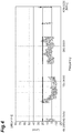
- FIG. 4 and FIG. 5 are obtained by measurement of variation in noise detected by an input filter in a case where an electromagnetic shield, that is, the base plate 11 or the protruding part 15, is provided between a power component and a filter component (input filter).
- FIG. 4 is obtained by measurement of noise detected by an input filter in a case where an electromagnetic shield is not provided
- FIG. 5 is obtained by measurement of noise detected in a case where a shield is provided between a power component and an input filter.
- FIG. 4 and FIG. 5 show results of measurement of only a noise component in a horizontal direction. It is noted that an aluminum plate with a thickness of 0.6 mm is used as each of the base plate 11, the bottom surface 15a and the side wall 15b which form the protruding part 15.
- the input terminal 2 which is connected to the input filter 4 included in the filter component 24 is attached to the side walls 12 of the casing 10, to be located above the main circuit board 20 in the power supply device 1, the input terminal 2 may be attached in a position of an input terminal 2A shown in FIG. 2 , in other words, may be attached to the side wall 15b of the protruding part 15, to be located below the main circuit board 20.
- a radiation noise from the power component 22 can easily arrive at a bus bar or the like which connects the filter component 24 (input filter 4) and the input terminal 2.
- the protruding part 15 which can reduce a radiation noise for the filter component 24 on one hand, may possibly cause influences of a radiation noise from the power component 22 to be exerted via a bus bar or the like.
- the input terminal is attached to the side wall 15b of the protruding part 15, so that a noise for a connecting member which connects the input terminal 2 and the input filter 4 can be reduced.
- FIG. 6 is a bottom view of a power supply device 1A according to a first modification.
- the power supply device 1A is different from the power supply device 1 in that two protruding parts are provided.
- the power supply device 1 includes the protruding part 15 in which the input filter 4 connected to the input terminal 2 is housed as the filter component 24, but does not have any configuration which takes into account a radiation noise for the EMC filter 8 or the like on a side where the output terminal 3 is provided.
- the power supply device 1 A has a configuration in which a protruding part 16 is further provided on a side where the output terminal 3 is provided, so that while the input filter 4 or the like on a side where the input terminal 2 is provided is housed as the filter component 24 in the protruding part 15, the EMC filter 8 or the like on a side where the output terminal 3 is provided is housed as a filter component 25 in the protruding part 16.
- a choke coil, a capacitor and the like can be cited.
- a lead component discrete component
- the power supply device 1A can be configured in such a manner that such a component is housed in the protruding part 16.
- the flat surface 11a of the base plate 11 in which the fins 14 are attached to a rear surface thereof, is provided between the protruding part 15 and the protruding part 16 in the same manner as in the power supply device 1. As a result of this, heat can be suitably dissipated from the power component 22 on the main circuit board 20.
- the filter components 24, 25 are housed in the protruding parts 15, 16, respectively, a radiation noise which is received by the filter components 24, 25 from the power component 22 can be reduced. Also, like the power supply device 1, the power supply device 1A as a whole can be miniaturized.
- FIG. 7 is a bottom view of a power supply device 1B according to a second modification.
- the power supply device 1B is similar to the power supply device 1A in that two protruding parts are provided, but is different from the power supply device 1A in a shape of the protruding part 15.
- a size of the protruding part 15 can be reduced as in the power supply device 1B.
- to change a position where the input terminal 2 is attached in accordance with the protruding part 15 could shorten a length of a member connecting the filter component 24 (input filter 4) and the input terminal 2.
- the protruding parts 15, 16 can be placed near the input terminal 2 or the output terminal 3 because each of the protruding parts 15, 16 has a function of housing a component provided in a subsequent stage with respect the input terminal 2 or a component provided in a preceding stage with respect to the output terminal 3, as described above.
- the flat surface 11a of the base plate 11 is enlarged to be formed in an area obtained by size reduction of the protruding part 15, and a component different from the filter components 24, 25 is mounted on the flat surface 11a of the base plate 11.
- the fins 14 are formed also on a rear side of an added part of the flat surface 11a of the base plate 11, which is enlarged, and cool a rear side of the base plate 11.
- the protruding part 15 is provided in a direction in which the fins 14 extend in some cases. If the protruding part 15 is provided in a direction in which the fins 14 extend, movement of a part of air which moves along the fins 14 is retarded by the protruding part 15.
- a heat generating component such as the power component 22 is placed in an area different from an area in which the fins 14 and the protruding part 15 interfere with each other, in other words, in an area in which the fins 14 and the protruding part 15 do not interfere with each other, so that satisfactory cooling performance of the device as a whole can be ensured.
- FIG. 8 is a bottom view of a power supply device 1 C according to a third modification.
- the power supply device 1C is similar to the power supply device 1B in that the protruding part 15 is reduced in size, but is different from the power supply device 1B in that the protruding part 16 is not provided, and in a direction in which the fins 14 extend.
- the fins 14 are provided so as to extend in parallel with a side wall along a longer dimension, out of the side walls 12 of the casing 10. Accordingly, air blown by a cooling means such as an external fan or the like moves in a lengthwise direction of the casing 10.
- a direction in which the fins 14 extend is not limited to a specific direction, and can be appropriately changed. Also, even in a case where a direction in which the fins 14 extend is changed as in the power supply device 1C, it is possible to ensure satisfactory heat-dissipation performance of the device as a whole by placing a heat generating component such as the power component 22 in an area where the fins 14 and the protruding part 15 do not interfere with each other.
- the power supply device 1 may include a plurality of circuit boards.
- the power component 22 can be connected to any of the plurality of circuit boards.
- the above-described embodiment has dealt with a case where the power component 22 is mounted onto the main circuit board 20, there can be provided a configuration in which the power component 22 is not mounted on the main circuit board 20.
- the above-described embodiment has dealt with a configuration in which the protruding part 15 is provided on at least a side where the input terminal 2 is provided and the filter component 24 on a side where the input terminal 2 is provided is housed in the protruding part 15, there can be provided a configuration in which only the protruding part 16 is provided on a side where the output terminal 3 is provided and the filter component 25 on a side where the output terminal 3 is provided is housed in the protruding part 16.
- the above-described embodiment has dealt with a configuration in which most of the filter component 24 is housed in the protruding part 15, it is possible to attain a power supply device which can achieve reduction of influences of noise and miniaturization of the device so long as at least a part of the filter component 24 is housed in the protruding part 15.
Landscapes
- Engineering & Computer Science (AREA)
- Microelectronics & Electronic Packaging (AREA)
- Physics & Mathematics (AREA)
- Power Engineering (AREA)
- Thermal Sciences (AREA)
- Electromagnetism (AREA)
- Dc-Dc Converters (AREA)
- Shielding Devices Or Components To Electric Or Magnetic Fields (AREA)
- Cooling Or The Like Of Electrical Apparatus (AREA)
Abstract
Description
- The present invention relates to a power supply device.
- A power supply device in which a plurality of electronic components are mounted onto a board, suffers from a problem associated with a noise generated from the electronic components in some cases. Thus, various kinds of configurations for reducing influences of noise are discussed. Further, some electronic components generate heat to have a high temperature, and so, also a way of placement of a heat dissipating means for cooling electronic components in a power supply device is discussed (refer to Japanese Unexamined Patent Publication No.
2000-278936 - While a demand for miniaturization of a power supply device is increasing in recent years, it is not easy to make heat dissipation from mounted electronic components and noise reduction, compatible with miniaturization of a device.
- The present invention has been made in view of the above-described matters, and it is an object of the present invention to provide a power supply device which can achieve heat dissipation from mounted electronic components, reduction of influences of noise generated in the device, and miniaturization of the device.
- In order to achieve the object, a power supply device according to an embodiment of the present invention includes: a circuit board; a power component and a filter component configured to be connected to the circuit board; and a casing configured to house the circuit board, the power component, and the filter component, wherein the casing includes a base plate including a flat surface in which a fin for heat dissipation is provided on a bottom-surface side, and a protruding part which protrudes from the flat surface toward the fin, and the power component and the circuit board are placed on the flat surface, and the filter component is housed in the protruding part.
- As in the above-described power supply device, the power component which can possibly be a noise source and is mounted onto the circuit board, is placed on the flat surface of the base plate in the casing, together with the circuit board. The filter component is housed in the protruding part which protrudes from the flat surface toward the fin. As a result of this, the circuit board and the power component are cooled by the fin provided on a rear side of the flat surface, so that effects of dissipating heat from electronic components are maintained. Also, because of a configuration of the power supply device in which the filter component is housed in the protruding part, a noise from the power component can be prevented from arriving at the filter component, so that influences of noise generated in the device can be reduced. Further, there is no need to provide an additional shield or the like in order to reduce a noise received by the filter component. Moreover, because of a configuration in which the filter component which is likely to be increased in size is housed in the protruding part, miniaturization of the device can be achieved.
- Also, a lead component can be further housed in the protruding part.
- Because of a configuration in which also the lead component is housed in the protruding part of the base plate, influences of noise can be further reduced.
- Also, at least a part of the fin can be configured to extend in a direction in which the fin does not interfere with the protruding part.
- In a case where the fin extends in a direction in which the fin does not interfere with the protruding part, movement of air along the fin can be prevented from being hampered by the protruding part, so that cooling effects on a rear side of the flat surface of the power supply device, which are produced by the fin, can be enhanced.
- According to the present invention, a power supply device which can achieve heat dissipation from mounted electronic components, reduction of influences of noise generated in the power supply device, and miniaturization of the device, is provided.
-
-
FIG. 1 is a block diagram showing a functional configuration of a power supply device according to an embodiment of the present invention; -
FIG. 2 is a schematic cross-sectional view showing arrangement of respective elements in the power supply device according to the embodiment; -
FIG. 3 is a bottom view of the power supply device according to the embodiment; -
FIG. 4 shows results of measurement of noise detected by an input filter in a case where an electromagnetic shield is not provided between a power component and a filter component (input filter); -
FIG. 5 shows results of measurement of noise detected by the input filter in a case where the electromagnetic shield is provided between the power component and the filter component (input filter); -
FIG. 6 is a bottom view for describing a first modification of the power supply device; -
FIG. 7 is a bottom view for describing a second modification of the power supply device; and -
FIG. 8 is a bottom view for describing a third modification of the power supply device. - An embodiment for carrying out the present invention will be described below in detail with reference to accompanying drawings. Regarding description of the drawings, the same elements will be denoted by the same reference symbols, and duplicated description will be avoided.
-
FIG. 1 is a block diagram showing a functional configuration of a power supply device according to an embodiment of the present invention. Apower supply device 1 described in the present embodiment is a switching power supply device or the like which performs voltage conversion (step-down) on a direct-current voltage which is input from a high-pressure battery connected to an input terminal, and produces a desired direct-current output voltage, for example. Also,FIG. 2 is a schematic cross-sectional view showing arrangement of respective elements in thepower supply device 1, andFIG. 3 is a bottom view of thepower supply device 1. - As shown in
FIG. 1 , thepower supply device 1 includes aninput filter 4, aswitching circuit 5, a high-frequency transformer 6, asmoothing filter 7, and anEMC filter 8 between aninput terminal 2 and anoutput terminal 3. Theinput filter 4, theswitching circuit 5, the high-frequency transformer 6, thesmoothing filter 7, and theEMC filter 8 are formed by combinations of electronic components and a circuit board. For example, theinput filter 4 includes a choke coil and the like. Theswitching circuit 5 includes a switching element of a transistor or the like. The high-frequency transformer 6 includes a transformer core, an inductor, and the like. Thesmoothing filter 7 includes a rectifier circuit element, a choke coil or an electrolytic capacitor, and the like. Also, the EMCfilter 8 includes a capacitor for a noise filter, and the like. Further, theinput filter 4, theswitching circuit 5, the high-frequency transformer 6, thesmoothing filter 7, and theEMC filter 8 are electrically connected with each other by conductive components or the like such as a circuit pattern formed in a main circuit board (main circuit board 20 inFIG. 2 ) or a bus bar. When those elements operate, thepower supply device 1 fulfills a desired function thereof. - Out of respective functional parts forming the
power supply device 1, theinput filter 4, theswitching circuit 5, the high-frequency transformer 6, thesmoothing filter 7, and the EMCfilter 8 are housed in acasing 10. Then, theinput terminal 2 and theoutput terminal 3 connect an inside and an outside of thecasing 10, and connect thepower supply device 1 and an external device. - Out of electronic components included in the respective functional parts forming the
power supply device 1, electronic components included in theswitching circuit 5, the high-frequency transformer 6, and thesmoothing filter 7 include an electronic component which can possibly be a noise source. When a switching operation is performed in thepower supply device 1, a switching noise is generated from a switching element, a rectifier circuit element, or the like in the electronic components in some cases. As such, an electronic component which can possibly generate a switching noise is an electronic component which can possibly be a noise source. In the present embodiment, such an electronic component will be referred to as a power component. - On the other hand, an electronic component which is likely to be affected when a switching noise is generated in the
power supply device 1 is also included in thepower supply device 1. In other words, out of electronic components included in the respective functional parts forming thepower supply device 1, electronic components included in theinput filter 4 and theEMC filter 8 are likely to be subjected to impairment of functions thereof due to reception of a switching noise in thepower supply device 1. Each of theinput filter 4 and theEMC filter 8, which is provided near theinput terminal 2 or theoutput terminal 3, has originally a function of suppressing a noise which is transmitted on a wire extending to, or coming from, an outside. However, upon reception of a switching noise which is internally generated, each of theinput filter 4 and theEMC filter 8 cannot satisfactorily fulfil a noise-suppressing function which is originally provided therein. Then, in thepower supply device 1 according to the present embodiment, respective positions of an electronic component which can possibly be a noise source and an electronic component which is affected by a noise are changed, so that noise reduction in thepower supply device 1 is achieved. - As shown in
FIG. 2 , thecasing 10 forms a part of a metallic case which houses composing members of thepower supply device 1. Thecasing 10 includes abase plate 11 forming a bottom, andside walls 12 surrounding thebase plate 11. In thepower supply device 1, after the above-described main circuit board 20 (circuit board) and electronic components are housed in thecasing 10, thecasing 10 is covered with acover 13. - The
casing 10 is made of metal such as aluminum, and has a substantially rectangular shape in plan view. Fins 14 for heat dissipation are attached to a rear side of aflat surface 11 a of thebase plate 11. Further, in an area different from theflat surface 11a of thebase plate 11, a bottom surface protrudes toward thefins 14, so that aprotruding part 15 in which a space is formed within thecasing 10 is formed. The protrudingpart 15 includes abottom surface 15a and aside wall 15b with which a periphery of thebottom surface 15a is covered. A part of theside wall 15b which is connected to theside walls 12 of thecasing 10, forms a surface continuous with theside walls 12. Also, thebottom surface 15a of theprotruding part 15 is designed so as to be at the same level as tips of the fins 14 (refer toFIG. 2 ). As a result of this, a sufficient volume of a space in the protrudingpart 15 can be ensured while an increase in size of thepower supply device 1 as a whole can be avoided. Description will be made later in those respects. - Also, the
input terminal 2 and theoutput terminal 3, by which an inside and an outside of thecasing 10 communicate with each other, are attached to theside walls 12 of thecasing 10. Theinput terminal 2 and theoutput terminal 3 are respectively provided on twoside walls 12 which are opposite to each other along shorter dimensions, out of theside walls 12 of thecasing 10 having a substantially rectangular shape in plan view. Accordingly, a flow path for electricity, which extends from theinput terminal 2 on one of the twoside walls 12 which are opposite to each other along shorter dimensions, to theoutput terminal 3 on the other of the twoside walls 12, is formed in thecasing 10. - As shown in
FIG. 3 , thefins 14 for heat dissipation in thepower supply device 1 are provided so as to extend in parallel with a side wall along a shorter dimension, out of theside walls 12 of thecasing 10. In thepower supply device 1, air is caused to move along thefins 14 by a cooling means such as an external fan. As a result of this, air moving along thefins 14 functions as a cooling medium, so that a rear side of theflat surface 11 a of thebase plate 11 is cooled. Consequently, heat generated in each of electronic components of thepower supply device 1 which are fixed to a front side of thebase plate 11 is transferred to thebase plate 11, and is dissipated to an outside from a rear side of theflat surface 11a of thebase plate 11. In this way, thebase plate 11 serves as a heatsink having a heat-dissipation function. - Besides, as shown in
FIG. 3 , thefins 14 are designed so as to extend in a direction in which thefins 14 do not interfere with the protrudingpart 15. That is, a direction in which thefins 14 extend is set in such a manner that movement of air which moves along thefins 14 is not hampered by the protrudingpart 15. Accordingly, cooling effects on a rear side of thebase plate 11, which are produced by thefins 14, can be enhanced. - Referring back to
FIG. 2 , arrangement of respective members of thepower supply device 1 which are provided in thecasing 10, will be described. Themain circuit board 20 is placed on theflat surface 11a of thebase plate 11 in thecasing 10. Also, out of electronic components connected to themain circuit board 20, an electronic component which can possibly be a noise source, that is, apower component 22, is mounted in a position on themain circuit board 20 and also on theflat surface 11a of thebase plate 11. While thepower component 22 can possibly be a noise source, thepower component 22 is also a so-called heat generating component which is likely to have a high temperature in many cases. Thus, thepower component 22 is mounted in a position on themain circuit board 20 and also on theflat surface 11a of thebase plate 11. This allows heat generated in thepower component 22 to be dissipated via themain circuit board 20 and theflat surface 11a of thebase plate 11. Consequently, heat-dissipation performance of thepower supply device 1 as a whole can be enhanced. - Also, a
filter component 24 different from thepower component 22 is housed in the protrudingpart 15 of thecasing 10. As thefilter component 24, theinput filter 4 can be cited for example, in the present embodiment. In such a configuration, theinput terminal 2 is connected to theinput filter 4 in the protrudingpart 15 via a bus bar or the like. Also, theoutput terminal 3 is connected to themain circuit board 20 via a bus bar or the like. - The above-described
power supply device 1 can be configured in such a manner that a component not included in thepower component 22, that is, a component different from an electronic component which is a noise source, is housed in the protrudingpart 15, similarly to thefilter component 24. As a component which can be housed in the protrudingpart 15, a lead component (discrete component) which is provided in a subsequent stage with respect to theinput filter 4 and in a preceding stage with respect to theswitching circuit 5, can be cited. If a lead component (discrete component) receives a noise from thepower component 22, a conduction noise may probably be given to thefilter component 24. Thus, also a lead component (discrete component) is a component which is preferably prevented from receiving a noise from thepower component 22. As such, by housing a lead component (discrete component) in the protrudingpart 15, it is possible to achieve noise reduction. Particularly in a case where a lead component (discrete component) is taller than the other electronic components, it is useful for miniaturization of thepower supply device 1 to house a lead component (discrete component) in the protrudingpart 15. - Effects produced by configuring the
power supply device 1 according to the present embodiment in the above-described manner, will be described. As described above, in thepower supply device 1, a switching noise which is generated from thepower component 22 during a switching operation may probably affect thefilter component 24 such as theinput filter 4. In this regard, a switching noise which may probably affect thefilter component 24 is mainly a radiation noise. When there is a considerable amount of radiation noise, thefilter component 24 cannot satisfactorily perform filtering on a noise which is provided from thepower supply device 1 to an outside, in some cases. - In an effort to prevent the
filter component 24 from being affected by a radiation noise caused by thepower component 22, use of a way of protecting thefilter component 24 with an electromagnetic shield is considered. However, to cover some of components of thepower supply device 1 with an electromagnetic shield would probably bring about an increase in size of the device. Thus, in circumstances where there is a demand for miniaturization of a device, it is not considered that to cover some of components of thepower supply device 1 with an electromagnetic shield is a practical solution. - In contrast thereto, in the
power supply device 1 according to the preset embodiment, thefilter component 24 is housed in the protrudingpart 15, so that a part of thecasing 10 which serves as a frame ground can function as a substitute for an electromagnetic shield. Broken lines L1 inFIG. 2 are lines connecting respective ends of thepower component 22 and thefilter component 24, and an area surrounded by two broken lines L1 inFIG. 2 is an area which is supposed to be a course on which a radiation noise is transferred from thepower component 22 directly to thefilter component 24. Then, in a part of the area surrounded by the two broken lines L1 inFIG. 2 , theflat surface 11a of thebase plate 11 of thecasing 10 and theside wall 15b of the protrudingpart 15 are provided between thepower component 22 and thefilter component 24. Accordingly, a radiation noise is prevented from being transferred from thepower component 22 directly to thefilter component 24. As such, by housing thefilter component 24 in the protrudingpart 15, it is possible to reduce a radiation noise caused by thepower component 22, and suppress influences of noise upon thefilter component 24. - Also, in the
power supply device 1, thepower component 22, in other words, a heat generating component which is likely to have a high temperature, is provided on themain circuit board 20 which is placed on theflat surface 11a of thebase plate 11, so that heat can be satisfactorily dissipated from thepower component 22. - Further, by housing the
filter component 24 in the protrudingpart 15, it is possible to miniaturize the device while achieving heat dissipation from electronic components and noise reduction. In thepower supply device 1, thefilter component 24 is taller than the other electronic components in some cases. Thus, if thefilter component 24 is mounted on theflat surface 11a of thebase plate 11 of the casing 10 (or on themain circuit board 20 which is placed on theflat surface 11a of the base plate 11), there is caused a need to set a height of theside walls 12 in thecasing 10 of thepower supply device 1 in accordance with a height of thefilter component 24 in some cases. That is, miniaturization (miniaturization particularly in a height direction; reduction in height) of thepower supply device 1 is hampered due to a height of thefilter component 24 in some cases. - In contrast thereto, in the
power supply device 1 according to the present embodiment, thefilter component 24 is housed in the protrudingpart 15, which eliminates a need to place thefilter component 24 above theflat surface 11a of thebase plate 11 in thepower supply device 1, so that reduction in height can be achieved. Thefins 14 which are to be provided on a rear side of theflat surface 11a of thebase plate 11, are provided over a whole of a bottom surface of thecasing 10 in a conventional art because a whole of a bottom surface of thecasing 10 is theflat surface 11 a of thebase plate 11. Each of thefins 14, which is a member for forming an air passage, should have a height commensurate with a required cooling capability. In thepower supply device 1 according to the present embodiment, a part of thefins 14 which are otherwise provided over a whole of a bottom surface of thecasing 10, is replaced with the protrudingpart 15, and thefilter component 24 is housed in the protrudingpart 15. Because of such a configuration, an upper end of thefilter component 24 which is tall can be prevented from upwardly protruding from the other electronic components. Also, thebottom surface 15a of the protrudingpart 15 is designed so as to be at the same level as respective lower ends of thefins 14, so that an increase in size of thepower supply device 1 which may be caused by provision of the protrudingpart 15 can be prevented. - Moreover, in the
power supply device 1, thefilter component 24 is housed in the protrudingpart 15, so that noise reduction for thefilter component 24 is achieved. In a case where thefilter component 24 is placed at the same level as themain circuit board 20 or the like, a shield or the like should be additionally provided in order to reduce a noise. However, in thepower supply device 1, it is unnecessary to additionally provide a shield or the like. Also in this respect, miniaturization of thepower supply device 1 can be achieved. - Besides, the
power component 22 which is a heat generating component being strongly required to be cooled with the use of thefins 14, is provided on themain circuit board 20 placed on theflat surface 11a of thebase plate 11. Accordingly, internal electronic components are prevented from being insufficiently cooled due to replacement of a part of thefins 14 with the protrudingpart 15. Also, thefilter component 24 housed in the protrudingpart 15 is not a heat generating component which is more likely to have a high temperature than the other electronic components, so that heat-dissipation performance of thepower supply device 1 as a whole is not affected even though thefilter component 24 is not placed on a rear side of thefins 14. In the above-described manner, thepower supply device 1 according to the present embodiment has a configuration in which the protrudingpart 15 is provided and thefilter component 24 is housed in the protrudingpart 15, to thereby achieve miniaturization of the device while achieving heat dissipation from electronic components and noise reduction. - Also, in a case where a lead component (discrete component) is taller than the other electronic components, a lead component, as well as the
filter component 24, is housed in the protrudingpart 15. As a result of such a configuration, further miniaturization of the device can be achieved. - Now, effects produced by provision of an electromagnetic shield in the
filter component 24 will be described with reference toFIG. 4 andFIG. 5 .FIG. 4 andFIG. 5 are obtained by measurement of variation in noise detected by an input filter in a case where an electromagnetic shield, that is, thebase plate 11 or the protrudingpart 15, is provided between a power component and a filter component (input filter).FIG. 4 is obtained by measurement of noise detected by an input filter in a case where an electromagnetic shield is not provided, andFIG. 5 is obtained by measurement of noise detected in a case where a shield is provided between a power component and an input filter.FIG. 4 andFIG. 5 show results of measurement of only a noise component in a horizontal direction. It is noted that an aluminum plate with a thickness of 0.6 mm is used as each of thebase plate 11, thebottom surface 15a and theside wall 15b which form the protrudingpart 15. - As a result of comparison between
FIG. 4 andFIG. 5 , it is confirmed that a noise in a frequency range higher than 200 MHz is particularly reduced by provision of thebase plate 11 or theside wall 15b of the protrudingpart 15 as an electromagnetic shield, between thepower component 22 and thefilter component 24. As such, it is confirmed that a noise in thefilter component 24 is reduced as a result of thefilter component 24 being housed in the protrudingpart 15. - Besides, though the
input terminal 2 which is connected to theinput filter 4 included in thefilter component 24 is attached to theside walls 12 of thecasing 10, to be located above themain circuit board 20 in thepower supply device 1, theinput terminal 2 may be attached in a position of aninput terminal 2A shown inFIG. 2 , in other words, may be attached to theside wall 15b of the protrudingpart 15, to be located below themain circuit board 20. In a case where theinput terminal 2 is attached in a position above themain circuit board 20, a radiation noise from thepower component 22 can easily arrive at a bus bar or the like which connects the filter component 24 (input filter 4) and theinput terminal 2. Thus, provision of the protrudingpart 15, which can reduce a radiation noise for thefilter component 24 on one hand, may possibly cause influences of a radiation noise from thepower component 22 to be exerted via a bus bar or the like. In view of this matter, the input terminal is attached to theside wall 15b of the protrudingpart 15, so that a noise for a connecting member which connects theinput terminal 2 and theinput filter 4 can be reduced. - Additionally, though the above-described embodiment has dealt with an example of the protruding
part 15 provided in thepower supply device 1, a way of placing the protrudingpart 15 can be appropriately changed. Below, while some modifications will be described, modifications of thepower supply device 1 are not limited to the following examples. - First,
FIG. 6 is a bottom view of apower supply device 1A according to a first modification. Thepower supply device 1A is different from thepower supply device 1 in that two protruding parts are provided. - The
power supply device 1 includes the protrudingpart 15 in which theinput filter 4 connected to theinput terminal 2 is housed as thefilter component 24, but does not have any configuration which takes into account a radiation noise for theEMC filter 8 or the like on a side where theoutput terminal 3 is provided. In contrast thereto, thepower supply device 1 A has a configuration in which a protrudingpart 16 is further provided on a side where theoutput terminal 3 is provided, so that while theinput filter 4 or the like on a side where theinput terminal 2 is provided is housed as thefilter component 24 in the protrudingpart 15, theEMC filter 8 or the like on a side where theoutput terminal 3 is provided is housed as afilter component 25 in the protrudingpart 16. As thefilter component 25 on a side where theoutput terminal 3 is provided, a choke coil, a capacitor and the like can be cited. If a lead component (discrete component) such as an electrolytic capacitor is included in theEMC filter 8, thepower supply device 1A can be configured in such a manner that such a component is housed in the protrudingpart 16. Theflat surface 11a of thebase plate 11 in which thefins 14 are attached to a rear surface thereof, is provided between the protrudingpart 15 and the protrudingpart 16 in the same manner as in thepower supply device 1. As a result of this, heat can be suitably dissipated from thepower component 22 on themain circuit board 20. Also, because of a configuration in which thefilter components parts filter components power component 22 can be reduced. Also, like thepower supply device 1, thepower supply device 1A as a whole can be miniaturized. -
FIG. 7 is a bottom view of apower supply device 1B according to a second modification. Thepower supply device 1B is similar to thepower supply device 1A in that two protruding parts are provided, but is different from thepower supply device 1A in a shape of the protrudingpart 15. - For example, in a case where the
filter component 24 which is to be housed in the protrudingpart 15 is small, a size of the protrudingpart 15 can be reduced as in thepower supply device 1B. In this case, to change a position where theinput terminal 2 is attached in accordance with the protrudingpart 15 could shorten a length of a member connecting the filter component 24 (input filter 4) and theinput terminal 2. The protrudingparts input terminal 2 or theoutput terminal 3 because each of the protrudingparts input terminal 2 or a component provided in a preceding stage with respect to theoutput terminal 3, as described above. Theflat surface 11a of thebase plate 11 is enlarged to be formed in an area obtained by size reduction of the protrudingpart 15, and a component different from thefilter components flat surface 11a of thebase plate 11. Thefins 14 are formed also on a rear side of an added part of theflat surface 11a of thebase plate 11, which is enlarged, and cool a rear side of thebase plate 11. In this example, as shown inFIG. 7 , the protrudingpart 15 is provided in a direction in which thefins 14 extend in some cases. If the protrudingpart 15 is provided in a direction in which thefins 14 extend, movement of a part of air which moves along thefins 14 is retarded by the protrudingpart 15. In such an area, cooling performance provided by air cooling cannot be satisfactorily delivered, as compared to an area where thefins 14 and the protrudingpart 15 do not interfere with each other. Thus, a heat generating component such as thepower component 22 is placed in an area different from an area in which thefins 14 and the protrudingpart 15 interfere with each other, in other words, in an area in which thefins 14 and the protrudingpart 15 do not interfere with each other, so that satisfactory cooling performance of the device as a whole can be ensured. -
FIG. 8 is a bottom view of a power supply device 1 C according to a third modification. The power supply device 1C is similar to thepower supply device 1B in that the protrudingpart 15 is reduced in size, but is different from thepower supply device 1B in that the protrudingpart 16 is not provided, and in a direction in which thefins 14 extend. - In the power supply device 1C, the
fins 14 are provided so as to extend in parallel with a side wall along a longer dimension, out of theside walls 12 of thecasing 10. Accordingly, air blown by a cooling means such as an external fan or the like moves in a lengthwise direction of thecasing 10. As such, a direction in which thefins 14 extend is not limited to a specific direction, and can be appropriately changed. Also, even in a case where a direction in which thefins 14 extend is changed as in the power supply device 1C, it is possible to ensure satisfactory heat-dissipation performance of the device as a whole by placing a heat generating component such as thepower component 22 in an area where thefins 14 and the protrudingpart 15 do not interfere with each other. - While the power supply devices according to one embodiment of the present invention have been described hereinabove, the present invention is not limited to the above-described embodiment.
- For example, though the above-described embodiment has dealt with a case where only a single circuit board (main circuit board 20) is housed in the
casing 10, thepower supply device 1 may include a plurality of circuit boards. In such a case, thepower component 22 can be connected to any of the plurality of circuit boards. Also, though the above-described embodiment has dealt with a case where thepower component 22 is mounted onto themain circuit board 20, there can be provided a configuration in which thepower component 22 is not mounted on themain circuit board 20. - Further, though the above-described embodiment has dealt with a configuration in which the protruding
part 15 is provided on at least a side where theinput terminal 2 is provided and thefilter component 24 on a side where theinput terminal 2 is provided is housed in the protrudingpart 15, there can be provided a configuration in which only the protrudingpart 16 is provided on a side where theoutput terminal 3 is provided and thefilter component 25 on a side where theoutput terminal 3 is provided is housed in the protrudingpart 16. Even in a case where a protruding part is provided on at least one of a side where theinput terminal 2 is provided and a side where theoutput terminal 3 is provided, and only a filter component on one of the above-stated sides is housed, influences of a noise can be reduced. Thus, it is possible to attain a power supply device which can achieve heat dissipation from mounted electronic components, reduction of influences of noise generated in the power supply device, and miniaturization of the device. - Moreover, though the above-described embodiment has dealt with a configuration in which most of the
filter component 24 is housed in the protrudingpart 15, it is possible to attain a power supply device which can achieve reduction of influences of noise and miniaturization of the device so long as at least a part of thefilter component 24 is housed in the protrudingpart 15.
Claims (3)
- A power supply device comprising:a circuit board;a power component and a filter component configured to be connected to the circuit board; anda casing configured to house the circuit board, the power component, and the filter component, whereinthe casing includes a base plate including a flat surface in which a fin for heat dissipation is provided on a bottom-surface side, and a protruding part which protrudes from the flat surface toward the fin, andthe power component and the circuit board are placed on the flat surface, and the filter component is housed in the protruding part.
- The power supply device according to claim 1, whereina lead component is further housed in the protruding part.
- The power supply device according to claim 1, whereinat least a part of the fin extends in a direction in which the fin does not interfere with the protruding part.
Applications Claiming Priority (1)
| Application Number | Priority Date | Filing Date | Title |
|---|---|---|---|
| JP2016009036A JP6607053B2 (en) | 2016-01-20 | 2016-01-20 | Power supply |
Publications (1)
| Publication Number | Publication Date |
|---|---|
| EP3197253A1 true EP3197253A1 (en) | 2017-07-26 |
Family
ID=57851001
Family Applications (1)
| Application Number | Title | Priority Date | Filing Date |
|---|---|---|---|
| EP17152255.0A Withdrawn EP3197253A1 (en) | 2016-01-20 | 2017-01-19 | Power supply device |
Country Status (4)
| Country | Link |
|---|---|
| US (1) | US10412848B2 (en) |
| EP (1) | EP3197253A1 (en) |
| JP (1) | JP6607053B2 (en) |
| CN (1) | CN106992660A (en) |
Citations (5)
| Publication number | Priority date | Publication date | Assignee | Title |
|---|---|---|---|---|
| JP2000278936A (en) | 1999-03-19 | 2000-10-06 | Idec Izumi Corp | Switching power supply device |
| JP2002205610A (en) * | 2001-01-09 | 2002-07-23 | Honda Motor Co Ltd | Vehicle control device |
| US20090057006A1 (en) * | 2007-09-05 | 2009-03-05 | Kokusan Denki Co., Ltd. | Electronic unit and production method of the same |
| WO2012098780A1 (en) * | 2011-01-19 | 2012-07-26 | 三洋電機株式会社 | Inverter apparatus and moving body mounted therewith |
| DE102014202841A1 (en) * | 2013-03-26 | 2014-10-02 | Keihin Corporation | Electronic control device for vehicle |
Family Cites Families (9)
| Publication number | Priority date | Publication date | Assignee | Title |
|---|---|---|---|---|
| DE19983152T1 (en) * | 1999-02-24 | 2001-05-31 | Mitsubishi Electric Corp | Power driver device |
| JP2002134968A (en) * | 2000-10-25 | 2002-05-10 | Sony Computer Entertainment Inc | Circuit board unit, electronic equipment |
| WO2007080748A1 (en) * | 2006-01-16 | 2007-07-19 | Mitsubishi Electric Corporation | Drive circuit of motor and outdoor unit of air conditioner |
| JP2011234559A (en) * | 2010-04-28 | 2011-11-17 | Sanyo Electric Co Ltd | Inverter device and electric vehicle loaded with the same |
| JP5673857B2 (en) * | 2011-11-21 | 2015-02-18 | 株式会社オートネットワーク技術研究所 | DC-DC converter |
| JP5813582B2 (en) * | 2012-06-01 | 2015-11-17 | 株式会社日本自動車部品総合研究所 | Electrical equipment |
| US8922034B2 (en) * | 2012-07-27 | 2014-12-30 | Illinois Tool Works Inc. | Power converter for engine generator |
| JP2014044007A (en) * | 2012-08-27 | 2014-03-13 | Toshiba Corp | Outdoor unit of air conditioner |
| CN104682457B (en) * | 2013-11-26 | 2017-08-29 | 台达电子企业管理(上海)有限公司 | The charging device of electronic installation and automobile |
-
2016
- 2016-01-20 JP JP2016009036A patent/JP6607053B2/en active Active
-
2017
- 2017-01-18 US US15/408,761 patent/US10412848B2/en active Active
- 2017-01-19 EP EP17152255.0A patent/EP3197253A1/en not_active Withdrawn
- 2017-01-19 CN CN201710043951.0A patent/CN106992660A/en active Pending
Patent Citations (5)
| Publication number | Priority date | Publication date | Assignee | Title |
|---|---|---|---|---|
| JP2000278936A (en) | 1999-03-19 | 2000-10-06 | Idec Izumi Corp | Switching power supply device |
| JP2002205610A (en) * | 2001-01-09 | 2002-07-23 | Honda Motor Co Ltd | Vehicle control device |
| US20090057006A1 (en) * | 2007-09-05 | 2009-03-05 | Kokusan Denki Co., Ltd. | Electronic unit and production method of the same |
| WO2012098780A1 (en) * | 2011-01-19 | 2012-07-26 | 三洋電機株式会社 | Inverter apparatus and moving body mounted therewith |
| DE102014202841A1 (en) * | 2013-03-26 | 2014-10-02 | Keihin Corporation | Electronic control device for vehicle |
Also Published As
| Publication number | Publication date |
|---|---|
| CN106992660A (en) | 2017-07-28 |
| JP2017131038A (en) | 2017-07-27 |
| US20170208702A1 (en) | 2017-07-20 |
| JP6607053B2 (en) | 2019-11-20 |
| US10412848B2 (en) | 2019-09-10 |
Similar Documents
| Publication | Publication Date | Title |
|---|---|---|
| US9456530B2 (en) | DC-DC converter | |
| JP6104347B1 (en) | Power converter | |
| KR102461278B1 (en) | Method for making rf power amplifier module and rf power amplifier module, rf module, and base station | |
| JP5783212B2 (en) | Power supply | |
| JP6432460B2 (en) | DC-DC converter | |
| US10950555B2 (en) | Ultra-low profile package shielding technique using magnetic and conductive layers for integrated switching voltage regulator | |
| US20080198557A1 (en) | Heat-dissipating module | |
| US20120314374A1 (en) | Heat dissipating high power systems | |
| JP2019075917A (en) | Power conversion device | |
| JP2014207370A (en) | Printed board | |
| US9899818B2 (en) | Circuit assembly and electrical junction box | |
| JP5987163B2 (en) | Power converter | |
| JP2004165664A (en) | Shielding casing for electric circuits about heat sink | |
| EP2933833A1 (en) | Electromagnetic shielding device | |
| KR101360730B1 (en) | Cooling device and electronic device thereof | |
| US10412848B2 (en) | Power supply device | |
| EP3214911A1 (en) | Apparatus comprising a housing with an improved cooling | |
| CN110958771B (en) | An integrated circuit board and electronic equipment | |
| JP4958189B2 (en) | Integrated circuit mounting structure | |
| JP2001359280A (en) | Power supply | |
| JP2002324994A (en) | Transmission amplification unit for wireless communication device | |
| CN106469694A (en) | Electronic electric equipment | |
| US20160172267A1 (en) | Circuit device and method of manufacturing a circuit device for controlling a transmission of a vehicle | |
| US10375821B2 (en) | Converter mounting board | |
| JP2013012508A (en) | Electronic apparatus |
Legal Events
| Date | Code | Title | Description |
|---|---|---|---|
| PUAI | Public reference made under article 153(3) epc to a published international application that has entered the european phase |
Free format text: ORIGINAL CODE: 0009012 |
|
| AK | Designated contracting states |
Kind code of ref document: A1 Designated state(s): AL AT BE BG CH CY CZ DE DK EE ES FI FR GB GR HR HU IE IS IT LI LT LU LV MC MK MT NL NO PL PT RO RS SE SI SK SM TR |
|
| AX | Request for extension of the european patent |
Extension state: BA ME |
|
| 17P | Request for examination filed |
Effective date: 20180119 |
|
| RBV | Designated contracting states (corrected) |
Designated state(s): AL AT BE BG CH CY CZ DE DK EE ES FI FR GB GR HR HU IE IS IT LI LT LU LV MC MK MT NL NO PL PT RO RS SE SI SK SM TR |
|
| 17Q | First examination report despatched |
Effective date: 20200928 |
|
| STAA | Information on the status of an ep patent application or granted ep patent |
Free format text: STATUS: THE APPLICATION HAS BEEN WITHDRAWN |
|
| 18W | Application withdrawn |
Effective date: 20201204 |