EP3195789A1 - Endoscope and endoscope system - Google Patents
Endoscope and endoscope system Download PDFInfo
- Publication number
- EP3195789A1 EP3195789A1 EP16779825.5A EP16779825A EP3195789A1 EP 3195789 A1 EP3195789 A1 EP 3195789A1 EP 16779825 A EP16779825 A EP 16779825A EP 3195789 A1 EP3195789 A1 EP 3195789A1
- Authority
- EP
- European Patent Office
- Prior art keywords
- buffer
- imaging
- endoscope
- transmission cable
- signal
- Prior art date
- Legal status (The legal status is an assumption and is not a legal conclusion. Google has not performed a legal analysis and makes no representation as to the accuracy of the status listed.)
- Withdrawn
Links
- 238000003384 imaging method Methods 0.000 claims abstract description 103
- 230000005540 biological transmission Effects 0.000 claims abstract description 45
- 238000012545 processing Methods 0.000 claims description 34
- 239000011159 matrix material Substances 0.000 claims description 3
- 238000003780 insertion Methods 0.000 description 8
- 230000037431 insertion Effects 0.000 description 8
- 238000006243 chemical reaction Methods 0.000 description 6
- 239000003990 capacitor Substances 0.000 description 5
- 238000010586 diagram Methods 0.000 description 4
- 230000008859 change Effects 0.000 description 3
- 238000005401 electroluminescence Methods 0.000 description 2
- 238000001727 in vivo Methods 0.000 description 2
- 238000000034 method Methods 0.000 description 2
- 230000004075 alteration Effects 0.000 description 1
- 230000003321 amplification Effects 0.000 description 1
- 230000000295 complement effect Effects 0.000 description 1
- 238000012937 correction Methods 0.000 description 1
- 230000000694 effects Effects 0.000 description 1
- 239000000284 extract Substances 0.000 description 1
- 229910052736 halogen Inorganic materials 0.000 description 1
- 150000002367 halogens Chemical class 0.000 description 1
- 238000005286 illumination Methods 0.000 description 1
- 239000004973 liquid crystal related substance Substances 0.000 description 1
- 230000007257 malfunction Effects 0.000 description 1
- 229910044991 metal oxide Inorganic materials 0.000 description 1
- 150000004706 metal oxides Chemical class 0.000 description 1
- 238000012986 modification Methods 0.000 description 1
- 230000004048 modification Effects 0.000 description 1
- 238000003199 nucleic acid amplification method Methods 0.000 description 1
- 239000013307 optical fiber Substances 0.000 description 1
- 230000009467 reduction Effects 0.000 description 1
- 239000004065 semiconductor Substances 0.000 description 1
- 230000000087 stabilizing effect Effects 0.000 description 1
Images
Classifications
-
- A—HUMAN NECESSITIES
- A61—MEDICAL OR VETERINARY SCIENCE; HYGIENE
- A61B—DIAGNOSIS; SURGERY; IDENTIFICATION
- A61B1/00—Instruments for performing medical examinations of the interior of cavities or tubes of the body by visual or photographical inspection, e.g. endoscopes; Illuminating arrangements therefor
- A61B1/00002—Operational features of endoscopes
- A61B1/00025—Operational features of endoscopes characterised by power management
- A61B1/00027—Operational features of endoscopes characterised by power management characterised by power supply
- A61B1/00029—Operational features of endoscopes characterised by power management characterised by power supply externally powered, e.g. wireless
-
- A—HUMAN NECESSITIES
- A61—MEDICAL OR VETERINARY SCIENCE; HYGIENE
- A61B—DIAGNOSIS; SURGERY; IDENTIFICATION
- A61B1/00—Instruments for performing medical examinations of the interior of cavities or tubes of the body by visual or photographical inspection, e.g. endoscopes; Illuminating arrangements therefor
- A61B1/00002—Operational features of endoscopes
- A61B1/00004—Operational features of endoscopes characterised by electronic signal processing
- A61B1/00006—Operational features of endoscopes characterised by electronic signal processing of control signals
-
- A—HUMAN NECESSITIES
- A61—MEDICAL OR VETERINARY SCIENCE; HYGIENE
- A61B—DIAGNOSIS; SURGERY; IDENTIFICATION
- A61B1/00—Instruments for performing medical examinations of the interior of cavities or tubes of the body by visual or photographical inspection, e.g. endoscopes; Illuminating arrangements therefor
- A61B1/00002—Operational features of endoscopes
- A61B1/00004—Operational features of endoscopes characterised by electronic signal processing
- A61B1/00009—Operational features of endoscopes characterised by electronic signal processing of image signals during a use of endoscope
-
- A—HUMAN NECESSITIES
- A61—MEDICAL OR VETERINARY SCIENCE; HYGIENE
- A61B—DIAGNOSIS; SURGERY; IDENTIFICATION
- A61B1/00—Instruments for performing medical examinations of the interior of cavities or tubes of the body by visual or photographical inspection, e.g. endoscopes; Illuminating arrangements therefor
- A61B1/00112—Connection or coupling means
- A61B1/00114—Electrical cables in or with an endoscope
-
- A—HUMAN NECESSITIES
- A61—MEDICAL OR VETERINARY SCIENCE; HYGIENE
- A61B—DIAGNOSIS; SURGERY; IDENTIFICATION
- A61B1/00—Instruments for performing medical examinations of the interior of cavities or tubes of the body by visual or photographical inspection, e.g. endoscopes; Illuminating arrangements therefor
- A61B1/04—Instruments for performing medical examinations of the interior of cavities or tubes of the body by visual or photographical inspection, e.g. endoscopes; Illuminating arrangements therefor combined with photographic or television appliances
-
- A—HUMAN NECESSITIES
- A61—MEDICAL OR VETERINARY SCIENCE; HYGIENE
- A61B—DIAGNOSIS; SURGERY; IDENTIFICATION
- A61B1/00—Instruments for performing medical examinations of the interior of cavities or tubes of the body by visual or photographical inspection, e.g. endoscopes; Illuminating arrangements therefor
- A61B1/04—Instruments for performing medical examinations of the interior of cavities or tubes of the body by visual or photographical inspection, e.g. endoscopes; Illuminating arrangements therefor combined with photographic or television appliances
- A61B1/05—Instruments for performing medical examinations of the interior of cavities or tubes of the body by visual or photographical inspection, e.g. endoscopes; Illuminating arrangements therefor combined with photographic or television appliances characterised by the image sensor, e.g. camera, being in the distal end portion
- A61B1/051—Details of CCD assembly
-
- G—PHYSICS
- G02—OPTICS
- G02B—OPTICAL ELEMENTS, SYSTEMS OR APPARATUS
- G02B23/00—Telescopes, e.g. binoculars; Periscopes; Instruments for viewing the inside of hollow bodies; Viewfinders; Optical aiming or sighting devices
- G02B23/24—Instruments or systems for viewing the inside of hollow bodies, e.g. fibrescopes
- G02B23/2476—Non-optical details, e.g. housings, mountings, supports
- G02B23/2484—Arrangements in relation to a camera or imaging device
-
- H—ELECTRICITY
- H04—ELECTRIC COMMUNICATION TECHNIQUE
- H04N—PICTORIAL COMMUNICATION, e.g. TELEVISION
- H04N23/00—Cameras or camera modules comprising electronic image sensors; Control thereof
- H04N23/50—Constructional details
- H04N23/555—Constructional details for picking-up images in sites, inaccessible due to their dimensions or hazardous conditions, e.g. endoscopes or borescopes
Definitions
- the transmission cable 3 connects the endoscope 2 and the connector portion 5 to each other, and connects the endoscope 2 and the light source device 8 to each other.
- the transmission cable 3 transmits the imaging signal generated by the imaging unit 20 to the connector portion 5.
- the transmission cable 3 includes a cable, an optical fiber, or the like.
- the first chip 21 includes a light receiving unit 23 including a plurality of pixels arranged in a two-dimensional matrix, receiving external light, and generating and outputting the imaging signal according to an amount of light received, a read unit 24 reading the imaging signal obtained by photoelectrical conversion by the light receiving unit 23, a timing generation unit 25 generating a timing signal based on a reference clock signal and a synchronization signal input from the connector portion 5, and outputting the timing signal to the read unit 24, and a first buffer 26 amplifying the imaging signal read from the light receiving unit 23 by the read unit 24 and applying a predetermined voltage to a second buffer 27 of the second chip 22 in a period in which the read unit 24 does not output the imaging signal read from the light receiving unit 23 to cause the second buffer 27 to output a direct current at a predetermined level to the transmission cable 3.
- the first buffer 26 will be described later with reference to FIG. 3 .
- the light receiving unit 23 and the read unit 24 function as the imaging element.
- the clock generating unit 63 generates the reference clock signal serving as a reference of the operation of each component unit of the endoscope system 1, and outputs this reference clock signal to the AFE unit 52, the imaging signal processing unit 53, the drive signal generating unit 54, and the image signal processing unit 62.
- the current mirror circuit 265 duplicates a current determined using on-resistance of the first transistor and the second transistor, from a fourth transistor 265a to a fifth transistor 265b.
- the fifth transistor 265b includes a PMOS transistor.
- the power supply voltage VDD is connected to a source
- the third transistor 266 is connected to a drain
- the drain side of the first transistor 262 is connected to a gate.
- a predetermined voltage for example, 1 V
- VDD a predetermined voltage obtained by dividing the power supply voltage VDD
- the second buffer 27 is brought into an on-state.
- the direct current is output at a predetermined level to the transmission cable 3 and it follows that current is consumed.
- This current consumption can prevent the high voltage of the power supply unit 61 from being applied to the imaging unit 20, due to a voltage drop of the transmission cable 3. Thereby, malfunction of the imaging unit 20, element breakage of the imaging unit 20, or the like can be reliably avoided.
Landscapes
- Health & Medical Sciences (AREA)
- Life Sciences & Earth Sciences (AREA)
- Surgery (AREA)
- Engineering & Computer Science (AREA)
- Physics & Mathematics (AREA)
- Optics & Photonics (AREA)
- Nuclear Medicine, Radiotherapy & Molecular Imaging (AREA)
- Medical Informatics (AREA)
- Biomedical Technology (AREA)
- Veterinary Medicine (AREA)
- Pathology (AREA)
- Radiology & Medical Imaging (AREA)
- Public Health (AREA)
- Heart & Thoracic Surgery (AREA)
- General Health & Medical Sciences (AREA)
- Biophysics (AREA)
- Molecular Biology (AREA)
- Animal Behavior & Ethology (AREA)
- Signal Processing (AREA)
- Multimedia (AREA)
- Computer Networks & Wireless Communication (AREA)
- Astronomy & Astrophysics (AREA)
- General Physics & Mathematics (AREA)
- Endoscopes (AREA)
- Instruments For Viewing The Inside Of Hollow Bodies (AREA)
- Studio Devices (AREA)
Abstract
Description
- The present invention relates to an endoscope inserted into a subject, imaging within the body of the subject, and generating image data, and an endoscope system.
- A technique is known wherein an imaging element such as a charge coupled device (CCD) or a complementary metal oxide semiconductor (CMOS) at a distal end of an insertion section of an endoscope, and an amplifier provided in the vicinity of the imaging element amplify an imaging signal output from the imaging element, and output the imaging signal to a processor (see Patent Literature 1). According to this technique, a pulse signal for driving the imaging element is used to generate a DC voltage applied to the imaging element and the amplifier, thereby reducing the number of power supply cables to reduce a diameter of the insertion section of the endoscope.
- Patent Literature 1:
JP 2003-153858 A - Incidentally, an imaging element provided in a conventional endoscope has a power supply in which a power supply cable is reduced in diameter with reduction in diameter of an insertion section of the endoscope, and resistance of the power supply cable increases. Therefore, in the conventional endoscope, power supply voltage is determined in consideration of voltage drop due to current consumption of the imaging element. However, as in the above-described
Patent Document 1, in an endoscope having a power supply cable reduced in diameter, when transmission of the pulse signal for driving an imaging element is stopped, the current consumption is considerably reduced and it follows that a high voltage is applied to the imaging element. As a result of this, the imaging element may be broken down. - The present invention has been made in view of the above problems, and it is an object of the present invention to provide an endoscope and an endoscope system in which application of a high voltage to an imaging element can be prevented, when transmission of a pulse signal for driving the imaging element is stopped. Solution to Problem
- To solve the problem described above and to achieve the object, an endoscope according to the present invention is an endoscope connected to a processing device performing predetermined image processing, through a transmission cable. The endoscope includes: a first chip including: an imaging element including a plurality of pixels arranged in a two-dimensional matrix and configured to receive external light, generate an imaging signal according to an amount of received light and output the generated imaging signal; and a first buffer configured to externally output the imaging signal generated by the imaging element; and a second chip including a second buffer configured to amplify the imaging signal output from the first buffer and output the amplified imaging signal to the transmission cable. The first buffer is configured to apply a predetermined voltage to the second buffer in a period in which the imaging element does not output the imaging signal to cause the second buffer to output a direct current at a predetermined level to the transmission cable.
- In the endoscope according to the present invention, the first buffer is configured to apply, to the second buffer, a voltage obtained by dividing a power supply voltage supplied from the processing device through the transmission cable.
- In the endoscope according to the present invention, the first buffer is a PMOS source follower transistor including a constant current source configured to be driven by a voltage obtained by dividing a power supply voltage supplied from the processing device, a gate configured to receive input of the imaging signal, and a source connected to the second buffer.
- An endoscope system according to the present invention includes: the endoscope according to the above-described invention; and a processing device including a drive signal generating unit configured to transmit a drive signal to the imaging element through the transmission cable, an image signal processing unit configured to receive the imaging signal amplified by the second buffer through the transmission cable, and a power supply unit configured to supply a power supply voltage to the imaging element, the first chip, and the second chip through the transmission cable.
- According to the present invention, it is possible to effectively prevent application of the high voltage to the imaging element when transmission of the pulse signal for driving the imaging element is stopped. Brief Description of Drawings
-
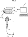
FIG. 1 is a schematic view illustrating an overall configuration of an endoscope system according to an embodiment of the present invention. -
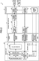
FIG. 2 is a block diagram illustrating a function of a main portion of the endoscope system according to an embodiment of the present invention. -
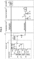
FIG. 3 is a circuit diagram illustrating detailed configurations of a first buffer, a second buffer, and a termination resistor illustrated inFIG. 2 . -
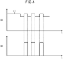
FIG. 4 is a schematic view illustrating change in current output from the second buffer. - An endoscope system including an endoscope with a distal end to be inserted into a subject will be described as a mode for carrying out the present invention (hereinafter referred to as "embodiment"). The present invention is not limited to this embodiment. Furthermore, in the description of the drawings, the same portions are denoted by the same reference signs. Still furthermore, it should be noted that the drawings are schematically illustrated, and relationships between the thicknesses and the widths, the proportions, or the like of members may be different from those of actual ones. In addition, the drawings include a portion which is different in size or proportion between the drawings.
-
FIG. 1 is a schematic view illustrating an overall configuration of the endoscope system according to an embodiment of the present invention. Anendoscope system 1 illustrated inFIG. 1 includes an endoscope 2, atransmission cable 3, aconnector portion 5, a processor 6 (processing device), adisplay device 7, alight source device 8, and aninput unit 9. - The endoscope 2 outputs an imaging signal (image data) to the
processor 6 by capturing an in-vivo image of the subject using aninsertion section 100, which is a part of thetransmission cable 3, inserted into a body of the subject. Furthermore, in the endoscope 2, an imaging unit 20 (imaging device) capturing the in-vivo image is provided, at one end of thetransmission cable 3, on the side of adistal end 101 of theinsertion section 100 to be inserted into a body cavity of the subject, and an operating unit 4 receiving various operations with respect to the endoscope 2 is connected on the side of aproximal end 102 of theinsertion section 100. Theimaging unit 20 is connected to theconnector portion 5 through the operating unit 4 by thetransmission cable 3. The Imaging signal of the image captured by theimaging unit 20 passes through, for example, thetransmission cable 3 having a length of several meters, and is output to theconnector portion 5. It should be noted that in the present embodiment, the endoscope 2 functions as the imaging device. - The
transmission cable 3 connects the endoscope 2 and theconnector portion 5 to each other, and connects the endoscope 2 and thelight source device 8 to each other. Thetransmission cable 3 transmits the imaging signal generated by theimaging unit 20 to theconnector portion 5. Thetransmission cable 3 includes a cable, an optical fiber, or the like. - The
connector portion 5 is connected to the endoscope 2, theprocessor 6, and thelight source device 8, performs predetermined signal processing on the imaging signal output from the endoscope 2 connected thereto, and performs analog-to-digital conversion (A/D conversion) on the imaging signal, and outputs the converted imaging signal as an image signal to theprocessor 6. - The
processor 6 performs predetermined image processing on the image signal output from theconnector portion 5, and generally controls thewhole endoscope system 1. It should be noted that in the present first embodiment, theprocessor 6 functions as the processing device. - The
display device 7 displays an image corresponding to the image signal subjected to the image processing by theprocessor 6. Thedisplay device 7 displays various information about theendoscope system 1. Thedisplay device 7 includes a liquid crystal or organic electro luminescence (EL) display panel. - The
light source device 8 includes, for example, a halogen lamp or a white light emitting diode (LED), and emits illumination light to the subject from the distal end side of theinsertion section 100 of the endoscope 2, through theconnector portion 5 and thetransmission cable 3. - The
input unit 9 includes, for example, a keyboard or a mouse, and receives input of information about various operations for theendoscope system 1. For example, theinput unit 9 receives input of an instruction signal for instructing amplification (gain-up) of the imaging signal from the endoscope 2 or a light intensity of thelight source device 8. -
FIG. 2 is a block diagram illustrating a function of a main portion of theendoscope system 1. A detailed configuration of each unit of theendoscope system 1 and an electrical signal path in theendoscope system 1 will be described with reference toFIG. 2 . As illustrated inFIG. 2 , theimaging unit 20 has a first chip 21 (imaging element), and asecond chip 22. - The
first chip 21 includes alight receiving unit 23 including a plurality of pixels arranged in a two-dimensional matrix, receiving external light, and generating and outputting the imaging signal according to an amount of light received, aread unit 24 reading the imaging signal obtained by photoelectrical conversion by thelight receiving unit 23, atiming generation unit 25 generating a timing signal based on a reference clock signal and a synchronization signal input from theconnector portion 5, and outputting the timing signal to theread unit 24, and afirst buffer 26 amplifying the imaging signal read from thelight receiving unit 23 by theread unit 24 and applying a predetermined voltage to asecond buffer 27 of thesecond chip 22 in a period in which theread unit 24 does not output the imaging signal read from thelight receiving unit 23 to cause thesecond buffer 27 to output a direct current at a predetermined level to thetransmission cable 3. It should be noted that a more detailed configuration of thefirst buffer 26 will be described later with reference toFIG. 3 . It should be noted that in the present embodiment, thelight receiving unit 23 and the readunit 24 function as the imaging element. - The
second chip 22 includes thesecond buffer 27 amplifying the imaging signal from each of the pixels, output from thefirst chip 21, and outputting the amplified imaging signal to thetransmission cable 3. It should be noted that a more detailed configuration of thesecond chip 22 will be described later with reference toFIG. 3 . - In addition, the
imaging unit 20 receives a power supply voltage VDD generated by a power supply unit 61 in theprocessor 6, and a ground (GND), through thetransmission cable 3. A capacitor C100 for stabilizing power supply is provided between the power supply voltage VDD and the ground (GND) supplied to theimaging unit 20. - The
connector portion 5 electrically connects the endoscope 2 (imaging unit 20) and theprocessor 6 to each other to function as a relay processing unit for relaying an electrical signal. Theconnector portion 5 and theimaging unit 20 are connected by thetransmission cable 3, and theconnector portion 5 and theprocessor 6 are connected by a coiled cable. Theconnector portion 5 is also connected to thelight source device 8. Theconnector portion 5 includes atermination resistor 51, an analog front end unit 52 (hereinafter, referred to as "AFE unit 52"), an imagingsignal processing unit 53, and a drive signal generating unit 54. - The
termination resistor 51 is provided at an end of thetransmission cable 3. It should be noted that a more detailed configuration of thetermination resistor 51 will be described later with reference toFIG. 3 . - The
AFE unit 52 receives the imaging signal transmitted from theimaging unit 20, performs impedance matching using a passive element such as a resistor, extracts an AC component in the capacitor, and then determines an operating point in a voltage divider. TheAFE unit 52 performs A/D conversion on an analog imaging signal transmitted from theimaging unit 20, and outputs the converted analog imaging signal to the imagingsignal processing unit 53 as a digital imaging signal. - The imaging
signal processing unit 53 performs predetermined signal processing, such as vertical line removal or noise removal, on the digital imaging signal input from theAFE unit 52, and outputs the imaging signal performed the predetermined signal processing to theprocessor 6. The imagingsignal processing unit 53 includes, for example, a field programmable gate array (FPGA). - On the basis of the reference clock signal (for example, a clock signal of 27 MHz) transmitted from the
processor 6, and serving as a reference of the operation of each component unit of the endoscope 2, the drive signal generating unit 54 generates the synchronization signal indicating a starting position of each frame, and outputs the synchronization signal to thetiming generation unit 25 of theimaging unit 20, through thetransmission cable 3, together with the reference clock signal. Here, the synchronization signal generated by the drive signal generating unit 54 includes a horizontal synchronization signal and a vertical synchronization signal. -
Processor 6 is a control device performing overall control of thewhole endoscope system 1. Theprocessor 6 includes the power supply unit 61, an imagesignal processing unit 62, and a clock generating unit 63. - The power supply unit 61 generates the power supply voltage VDD, and supplies the generated power supply voltage VDD and the ground (GND) to the
imaging unit 20 through theconnector portion 5 and thetransmission cable 3. - The image
signal processing unit 62 performs image processing, such as synchronization processing, white balance (WB) adjustment, gain adjustment, gamma correction, digital to analog (D/A) conversion, or format conversion, on the digital imaging signal subjected to the signal processing by the imagingsignal processing unit 53 to convert into the image signal, and outputs the converted image signal to thedisplay device 7. - The clock generating unit 63 generates the reference clock signal serving as a reference of the operation of each component unit of the
endoscope system 1, and outputs this reference clock signal to theAFE unit 52, the imagingsignal processing unit 53, the drive signal generating unit 54, and the imagesignal processing unit 62. - Next, the detailed configurations of main portions of the
first buffer 26, thesecond buffer 27, and thetermination resistor 51 will be described.FIG. 3 is a circuit diagram illustrating the detailed configurations of thefirst buffer 26, thesecond buffer 27, and thetermination resistor 51 illustrated inFIG. 2 . - As illustrated in
FIG. 3 , thefirst buffer 26 applies a voltage obtained by dividing the power supply voltage VDD supplied from the power supply unit 61 of theprocessor 6 through thetransmission cable 3, to thesecond buffer 27. Thefirst buffer 26 includes afirst voltage divider 261, afirst transistor 262, asecond voltage divider 263, asecond transistor 264, acurrent mirror circuit 265, athird transistor 266. - The
first voltage divider 261 includes afirst resistor 261a and asecond resistor 261b connected in series between the power supply voltage VDD and the ground, and applies a divided output voltage Vbias1 to a gate of thefirst transistor 262. - The
first transistor 262 includes an NMOS transistor. In thefirst transistor 262, thecurrent mirror circuit 265 is connected to a drain, thethird transistor 266 is connected to a source, and a connecting line receiving application of the output voltage Vbias1 from thefirst voltage divider 261 is connected to a gate. - The
second voltage divider 263 includes athird resistor 263a and afourth resistor 263b connected in series between the power supply voltage VDD and the ground, and applies a divided output voltage Vbias2 to a gate of thesecond transistor 264. - The
second transistor 264 includes an NMOS transistor. In thesecond transistor 264, thethird transistor 266 is connected to a drain, the ground is connected to a source, and a connecting line receiving application of the output voltage Vbias2 from thesecond voltage divider 263 is connected to a gate. - The
current mirror circuit 265 duplicates a current determined using on-resistance of the first transistor and the second transistor, from afourth transistor 265a to afifth transistor 265b. - The
fourth transistor 265a includes a PMOS transistor. In thefourth transistor 265a, the power supply voltage VDD is connected to a source, and the drain of thefirst transistor 262 is connected to a drain. - The
fifth transistor 265b includes a PMOS transistor. In thefifth transistor 265b, the power supply voltage VDD is connected to a source, thethird transistor 266 is connected to a drain, and the drain side of thefirst transistor 262 is connected to a gate. - The
third transistor 266 includes a PMOS source follower transistor. In thethird transistor 266, a constant current source is connected, and the constant current source is driven by a divided voltage divided by thecurrent mirror circuit 265 where the current determined using thefirst voltage divider 261 and thesecond voltage divider 263 is applied. Thecurrent mirror circuit 265 where the current determined using thefirst voltage divider 261 and thesecond voltage divider 263 is applied is connected to a source side. Furthermore, thesecond buffer 27 is connected to an output end (source side), and a connecting line transmitting the imaging signal Vin read from thelight receiving unit 23 by theread unit 24 is connected to an input end (gate side). - The
second buffer 27 includes an NMOS transistor. In thesecond buffer 27, the power supply voltage VDD is connected to a drain, thetransmission cable 3 externally transmitting the imaging signal Vout through animpedance resistor 28 for matching impedance of thetransmission cable 3 is connected to an output end (source side), and a signal line transmitting the imaging signal Vin output from thefirst chip 21 is connected to an input end (gate side). - The
connector portion 5 includes at least anAC termination resistor 503 connected to the GND, aDC termination resistor 502 connected to the GND, and aDC decoupling capacitor 504 decoupling the direct current output from thesecond chip 22. - Next, the change in current output from the
second buffer 27 will be described.FIG. 4 is a schematic view illustrating the change in current output from thesecond buffer 27. InFIG. 4 , the horizontal axis represents time, and the vertical axis represents values of current. Furthermore, (a) ofFIG. 4 represents the values of current output from thesecond buffer 27, and (b) ofFIG. 4 represents the clock signal. Furthermore, in (a) ofFIG. 4 , a square wave L1 represents the values of current output from thesecond buffer 27. - As illustrated in
FIG. 4 , when a predetermined voltage (for example, 1 V) obtained by dividing the power supply voltage VDD is applied from thefirst buffer 26 to thesecond buffer 27 under a condition other than normal operation, such as, before the clock signal is transmitted to theimaging unit 20, while the transmission of the clock signal is stopped, or at a time of starting up theendoscope system 1, thesecond buffer 27 is brought into an on-state. Thereby, the direct current is output at a predetermined level to thetransmission cable 3 and it follows that current is consumed. This current consumption can prevent the high voltage of the power supply unit 61 from being applied to theimaging unit 20, due to a voltage drop of thetransmission cable 3. Thereby, malfunction of theimaging unit 20, element breakage of theimaging unit 20, or the like can be reliably avoided. - According to an embodiment of the present invention described above, the
first buffer 26 applies a predetermined voltage to thesecond buffer 27 in a period in which theimaging unit 20 does not output the imaging signal to cause thesecond buffer 27 to output a predetermined direct current to thetransmission cable 3, so that it is possible to prevent the high voltage from being applied to theimaging unit 20 under a condition other than the normal operation, such as, at a time of starting up, or while transmission of a pulse signal is stopped. - It should be noted that in an embodiment of the present invention, the
third transistor 266 includes the PMOS, and thesecond buffer 27 includes the NMOS, but thethird transistor 266 may include an NMOS, and thesecond buffer 27 may include a PMOS. - The present invention can include various embodiments not described above, and various modifications and alterations may be made without departing from the spirit or scope of the technical scope as defined by the appended claims.
-
- 1
- ENDOSCOPE SYSTEM
- 2
- ENDOSCOPE
- 3
- TRANSMISSION CABLE
- 4
- OPERATING UNIT
- 5
- CONNECTOR PORTION
- 6
- PROCESSOR
- 7
- DISPLAY DEVICE
- 8
- LIGHT SOURCE DEVICE
- 9
- INPUT UNIT
- 20
- IMAGING UNIT
- 21
- FIRST CHIP
- 22
- SECOND CHIP
- 23
- LIGHT RECEIVING UNIT
- 24
- READ UNIT
- 25
- TIMING GENERATION UNIT
- 26
- FIRST BUFFER
- 27
- SECOND BUFFER
- 28
- IMPEDANCE RESISTOR
- 51
- TERMINATION RESISTOR
- 52
- AFE UNIT
- 53
- IMAGING SIGNAL PROCESSING UNIT
- 54
- DRIVE SIGNAL GENERATING UNIT
- 61
- POWER SUPPLY UNIT
- 62
- IMAGE SIGNAL PROCESSING UNIT
- 63
- CLOCK GENERATING UNIT
- 100
- INSERTION SECTION
- 101
- DISTAL END
- 102
- PROXIMAL END
- 261
- FIRST VOLTAGE DIVIDER
- 261a
- FIRST RESISTOR
- 261b
- SECOND RESISTOR
- 262
- FIRST TRANSISTOR
- 263
- SECOND VOLTAGE DIVIDER
- 263a
- THIRD RESISTOR
- 263b
- FOURTH RESISTOR
- 264
- SECOND TRANSISTOR
- 265
- CURRENT MIRROR CIRCUIT
- 265a
- FOURTH TRANSISTOR
- 265b
- FIFTH TRANSISTOR
- 266
- THIRD TRANSISTOR
- 502
- DC TERMINATION RESISTOR
- 503
- AC TERMINATION RESISTOR
- 504
- DC DECOUPLING CAPACITOR
- C100
- CAPACITOR
Claims (4)
- An endoscope connected to a processing device performing predetermined image processing, through a transmission cable, the endoscope comprising:a first chip including:an imaging element including a plurality of pixels arranged in a two-dimensional matrix and configured to receive external light, generate an imaging signal according to an amount of received light and output the generated the imaging signal; anda first buffer configured to externally output the imaging signal generated by the imaging element; anda second chip including a second buffer configured to amplify the imaging signal output from the first buffer and output the amplified imaging signal to the transmission cable,wherein the first buffer is configured to apply a predetermined voltage to the second buffer in a period in which the imaging element does not output the imaging signal to cause the second buffer to output a direct current at a predetermined level to the transmission cable.
- The endoscope according to claim 1, wherein
the first buffer is configured to apply, to the second buffer, a voltage obtained by dividing a power supply voltage supplied from the processing device through the transmission cable. - The endoscope according to claim 1, wherein
the first buffer is a PMOS source follower transistor including a constant current source configured to be driven by a voltage obtained by dividing a power supply voltage supplied from the processing device, a gate configured to receive input of the imaging signal, and a source connected to the second buffer. - An endoscope system comprising:the endoscope according to claim 1; anda processing device including a drive signal generating unit configured to transmit a drive signal to the imaging element through the transmission cable, an image signal processing unit configured to receive the imaging signal amplified by the second buffer through the transmission cable, and a power supply unit configured to supply a power supply voltage to the imaging element, the first chip, and the second chip through the transmission cable.
Applications Claiming Priority (2)
| Application Number | Priority Date | Filing Date | Title |
|---|---|---|---|
| JP2015084315 | 2015-04-16 | ||
| PCT/JP2016/055573 WO2016167033A1 (en) | 2015-04-16 | 2016-02-25 | Endoscope and endoscope system |
Publications (2)
| Publication Number | Publication Date |
|---|---|
| EP3195789A1 true EP3195789A1 (en) | 2017-07-26 |
| EP3195789A4 EP3195789A4 (en) | 2018-04-18 |
Family
ID=57126139
Family Applications (1)
| Application Number | Title | Priority Date | Filing Date |
|---|---|---|---|
| EP16779825.5A Withdrawn EP3195789A4 (en) | 2015-04-16 | 2016-02-25 | Endoscope and endoscope system |
Country Status (5)
| Country | Link |
|---|---|
| US (1) | US10506917B2 (en) |
| EP (1) | EP3195789A4 (en) |
| JP (1) | JP6028135B1 (en) |
| CN (1) | CN106714658B (en) |
| WO (1) | WO2016167033A1 (en) |
Families Citing this family (6)
| Publication number | Priority date | Publication date | Assignee | Title |
|---|---|---|---|---|
| JPWO2017056146A1 (en) * | 2015-09-28 | 2018-07-12 | オリンパス株式会社 | Signal transmission circuit and endoscope system |
| JP6883469B2 (en) * | 2017-05-09 | 2021-06-09 | オリンパス株式会社 | Endoscope |
| WO2019207762A1 (en) * | 2018-04-27 | 2019-10-31 | オリンパス株式会社 | Imaging system and endoscope system |
| JP7422133B2 (en) * | 2019-03-14 | 2024-01-25 | ソニーセミコンダクタソリューションズ株式会社 | Solid-state imaging device and imaging device |
| WO2022013953A1 (en) * | 2020-07-14 | 2022-01-20 | オリンパス株式会社 | Imaging system, endoscope, and control device |
| CN120916077B (en) * | 2025-10-10 | 2026-02-24 | 锐睛微电子(珠海)有限公司 | A relay adjustment circuit for an endoscope and an endoscope |
Family Cites Families (28)
| Publication number | Priority date | Publication date | Assignee | Title |
|---|---|---|---|---|
| JPS5652031A (en) * | 1979-10-02 | 1981-05-09 | Olympus Optical Co | Endoscope system |
| JP2559510B2 (en) * | 1989-04-06 | 1996-12-04 | オリンパス光学工業株式会社 | Electronic endoscopic device |
| JP2579372B2 (en) * | 1989-12-04 | 1997-02-05 | 日本テキサス・インスツルメンツ株式会社 | Low power imaging device |
| JP3041099B2 (en) * | 1991-02-01 | 2000-05-15 | オリンパス光学工業株式会社 | Electronic endoscope device |
| JP2002051969A (en) * | 2000-08-08 | 2002-02-19 | Asahi Optical Co Ltd | Electronic endoscope device |
| JP4132791B2 (en) | 2001-11-19 | 2008-08-13 | Hoya株式会社 | Electronic endoscope device |
| TWI259661B (en) * | 2004-01-08 | 2006-08-01 | Novatek Microelectronics Corp | Analog front end circuit and method thereof |
| JP2008148835A (en) * | 2006-12-15 | 2008-07-03 | Hoya Corp | Image signal transmission system, electronic endoscope, endoscope processor |
| JP2009272909A (en) * | 2008-05-08 | 2009-11-19 | Hoya Corp | Digital video signal transmission apparatus, receiver and including system |
| JP2011029793A (en) * | 2009-07-22 | 2011-02-10 | Panasonic Corp | Solid-state imaging apparatus and camera |
| JP2011109584A (en) * | 2009-11-20 | 2011-06-02 | Panasonic Corp | Solid-state image sensor and solid-state imaging device |
| JP5906596B2 (en) * | 2010-08-16 | 2016-04-20 | 株式会社ニコン | Imaging device |
| JP2012235193A (en) * | 2011-04-28 | 2012-11-29 | Canon Inc | Image sensor, imaging device, control method therefor, and control program |
| JP5362080B2 (en) * | 2011-10-07 | 2013-12-11 | キヤノン株式会社 | Solid-state imaging device and imaging system |
| JP5865210B2 (en) * | 2012-08-13 | 2016-02-17 | オリンパス株式会社 | Imaging system |
| JP6074200B2 (en) * | 2012-09-14 | 2017-02-01 | キヤノン株式会社 | Scanning circuit, solid-state imaging device, and camera |
| WO2014115390A1 (en) * | 2013-01-23 | 2014-07-31 | オリンパスメディカルシステムズ株式会社 | Image capture device, endoscope system, and noise reduction method |
| US20140300717A1 (en) * | 2013-04-08 | 2014-10-09 | Olympus Corporation | Endoscope apparatus |
| JP5826969B2 (en) * | 2013-04-18 | 2015-12-02 | オリンパス株式会社 | IMAGING ELEMENT, IMAGING DEVICE, ENDOSCOPE, ENDOSCOPE SYSTEM, AND IMAGING ELEMENT DRIVE METHOD |
| WO2014171316A1 (en) * | 2013-04-18 | 2014-10-23 | オリンパスメディカルシステムズ株式会社 | Image-capturing element, image-capturing device, and endoscope system |
| JP5826968B2 (en) * | 2013-04-25 | 2015-12-02 | オリンパス株式会社 | Imaging device, imaging device, endoscope, and endoscope system |
| WO2014175006A1 (en) * | 2013-04-25 | 2014-10-30 | オリンパスメディカルシステムズ株式会社 | Image sensor, imaging device, endoscope, endoscope system and driving method of image sensor |
| US20150038935A1 (en) * | 2013-08-05 | 2015-02-05 | Mcneil-Ppc, Inc. | Adhesive and Use for Attachment to Microfiber Garments |
| JP5767287B2 (en) * | 2013-09-13 | 2015-08-19 | オリンパス株式会社 | Imaging device |
| JP6351228B2 (en) * | 2013-09-30 | 2018-07-04 | オリンパス株式会社 | Imaging module and endoscope apparatus |
| JP6205228B2 (en) * | 2013-09-30 | 2017-09-27 | オリンパス株式会社 | Imaging module and endoscope apparatus |
| WO2016006302A1 (en) * | 2014-07-10 | 2016-01-14 | オリンパス株式会社 | Imaging element, imaging device, endoscope, endoscope system, and method for driving imaging element |
| JP5826977B1 (en) * | 2014-08-21 | 2015-12-02 | オリンパス株式会社 | Imaging device, endoscope, endoscope system, and driving method of imaging device |
-
2016
- 2016-02-25 WO PCT/JP2016/055573 patent/WO2016167033A1/en not_active Ceased
- 2016-02-25 JP JP2016543257A patent/JP6028135B1/en active Active
- 2016-02-25 CN CN201680002244.0A patent/CN106714658B/en active Active
- 2016-02-25 EP EP16779825.5A patent/EP3195789A4/en not_active Withdrawn
-
2017
- 2017-02-14 US US15/432,123 patent/US10506917B2/en active Active
Also Published As
| Publication number | Publication date |
|---|---|
| CN106714658B (en) | 2018-08-14 |
| US10506917B2 (en) | 2019-12-17 |
| JP6028135B1 (en) | 2016-11-16 |
| JPWO2016167033A1 (en) | 2017-04-27 |
| EP3195789A4 (en) | 2018-04-18 |
| WO2016167033A1 (en) | 2016-10-20 |
| CN106714658A (en) | 2017-05-24 |
| US20170150869A1 (en) | 2017-06-01 |
Similar Documents
| Publication | Publication Date | Title |
|---|---|---|
| US10506917B2 (en) | Endoscope and endoscope system with transmission buffer | |
| US9596977B2 (en) | Imaging element, imaging device, endoscope, endoscope system, and method of driving imaging element | |
| US9433338B2 (en) | Imaging element, imaging device, endoscope, endoscope system, and method of driving imaging element | |
| JP5981076B1 (en) | Imaging apparatus, drive signal adjustment method, and endoscope system | |
| EP3367667A1 (en) | Imaging device, endoscope, and endoscope system | |
| US11877053B2 (en) | Booster apparatus, imaging apparatus, endoscope and voltage conversion control method | |
| EP3157248A1 (en) | Imaging element, imaging device, endoscope, endoscope system, and method for driving imaging element | |
| US9693002B2 (en) | Image sensor, imaging device, endoscope, and endoscope system | |
| US9591233B2 (en) | Imaging device, endoscope, endoscope system, and method for driving imaging device | |
| WO2018088005A1 (en) | Imaging element and endoscope | |
| US20140300717A1 (en) | Endoscope apparatus | |
| US20190327414A1 (en) | Imaging device, endoscope, and endoscope system | |
| US20170245743A1 (en) | Endoscopic system and endoscope | |
| WO2016006302A1 (en) | Imaging element, imaging device, endoscope, endoscope system, and method for driving imaging element | |
| JP4132791B2 (en) | Electronic endoscope device | |
| US11206377B2 (en) | Imaging apparatus, imaging system, and imaging method | |
| US20180199802A1 (en) | Endoscope system | |
| JP6987666B2 (en) | Image sensor, image sensor, endoscope and endoscope system | |
| JP2019034074A (en) | Endoscope and processor | |
| JP2011139795A (en) | Endoscopic system | |
| JP2013013494A (en) | Electronic endoscope device |
Legal Events
| Date | Code | Title | Description |
|---|---|---|---|
| STAA | Information on the status of an ep patent application or granted ep patent |
Free format text: STATUS: THE INTERNATIONAL PUBLICATION HAS BEEN MADE |
|
| PUAI | Public reference made under article 153(3) epc to a published international application that has entered the european phase |
Free format text: ORIGINAL CODE: 0009012 |
|
| STAA | Information on the status of an ep patent application or granted ep patent |
Free format text: STATUS: REQUEST FOR EXAMINATION WAS MADE |
|
| 17P | Request for examination filed |
Effective date: 20170215 |
|
| AK | Designated contracting states |
Kind code of ref document: A1 Designated state(s): AL AT BE BG CH CY CZ DE DK EE ES FI FR GB GR HR HU IE IS IT LI LT LU LV MC MK MT NL NO PL PT RO RS SE SI SK SM TR |
|
| AX | Request for extension of the european patent |
Extension state: BA ME |
|
| A4 | Supplementary search report drawn up and despatched |
Effective date: 20180321 |
|
| RIC1 | Information provided on ipc code assigned before grant |
Ipc: A61B 1/04 20060101AFI20180315BHEP Ipc: G02B 23/24 20060101ALI20180315BHEP Ipc: H04N 5/378 20110101ALI20180315BHEP Ipc: A61B 1/05 20060101ALI20180315BHEP Ipc: A61B 1/00 20060101ALI20180315BHEP |
|
| DAV | Request for validation of the european patent (deleted) | ||
| DAX | Request for extension of the european patent (deleted) | ||
| STAA | Information on the status of an ep patent application or granted ep patent |
Free format text: STATUS: THE APPLICATION IS DEEMED TO BE WITHDRAWN |
|
| 18D | Application deemed to be withdrawn |
Effective date: 20200901 |